András Halbritter: Point contact Andreev spectroscopy · Point contact Andreev spectroscopy...
29
Budapest University of Technology and Economics Department of Physics Low temperature solid state physics laboratory Coworkers: Prof. György Mihály Dr. Szabolcs Csonka Attila Geresdi Péter Makk András Halbritter: Point contact Andreev spectroscopy correlated electron systems, magnetic semiconductors (Pressure cell (up to 30kBar), MOKE setup TEP measurements,heat conductivity measurements) MCBJ, Andreev spectroscopy
Transcript of András Halbritter: Point contact Andreev spectroscopy · Point contact Andreev spectroscopy...
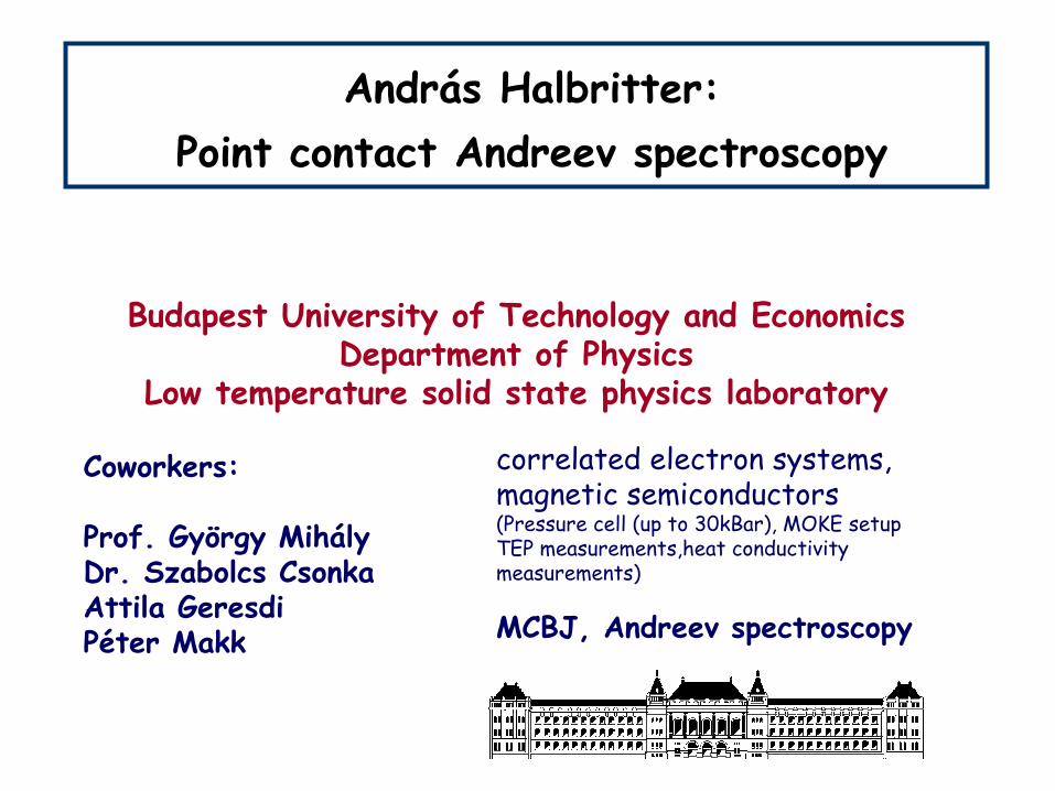
Budapest University of Technology and EconomicsDepartment of Physics
Low temperature solid state physics laboratory
Coworkers:
Prof. György MihályDr. Szabolcs Csonka Attila GeresdiPéter Makk
András Halbritter:Point contact Andreev spectroscopy
correlated electron systems, magnetic semiconductors(Pressure cell (up to 30kBar), MOKE setupTEP measurements,heat conductivitymeasurements)
MCBJ, Andreev spectroscopy
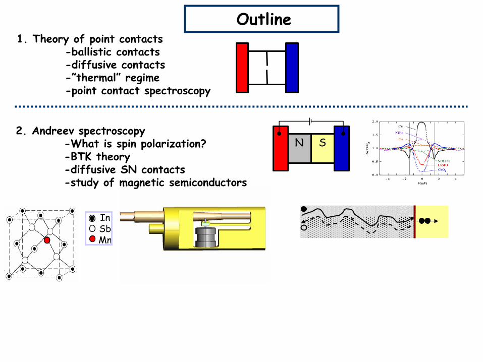
Outline1. Theory of point contacts
-ballistic contacts-diffusive contacts-”thermal” regime-point contact spectroscopy
2. Andreev spectroscopy-What is spin polarization? -BTK theory-diffusive SN contacts-study of magnetic semiconductors
N S
InSbMn
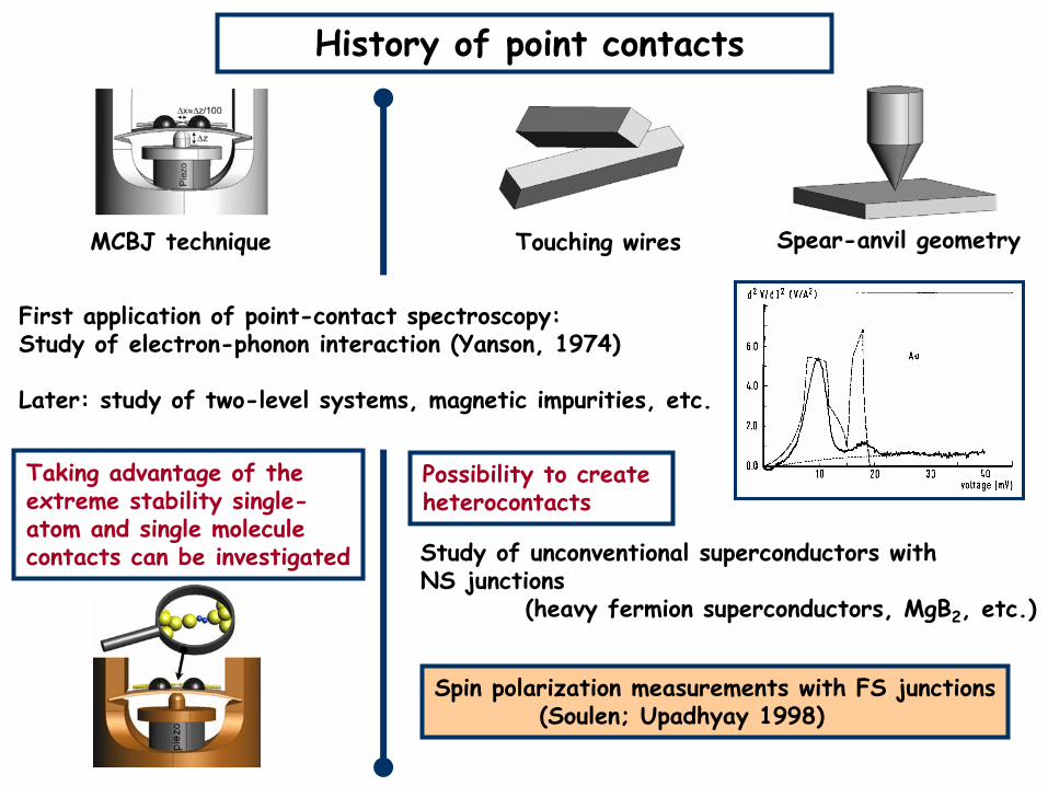
History of point contacts
MCBJ technique
First application of point-contact spectroscopy:Study of electron-phonon interaction (Yanson, 1974)
Later: study of two-level systems, magnetic impurities, etc.
Possibility to createheterocontacts
Taking advantage of theextreme stability single-atom and single moleculecontacts can be investigated
Touching wires Spear-anvil geometry
Study of unconventional superconductors withNS junctions
(heavy fermion superconductors, MgB2, etc.)
Spin polarization measurements with FS junctions(Soulen; Upadhyay 1998)
Distributionfunction atthe middle ofthe contact: kx
kydε=e
Vd
V
∑ ∫==k
kkkk rvkrvrj )()2(
d2)(2)( 3
3
sample
fefVe
π
kx
kykvheVk =d )0()0(d =⋅=== ∫ xjAxjAI xx
A
43421h
π
ϑπ
kv
kk
vv
2F
)cos()2(
2)0(
d
3
k
S
k
xeVexj ∫⋅⋅==
VdkheI
G
⋅
⋅=
4434421Sharvin
2F
2
42
Sharvin formula in 3D:
Ballistic point contacts
Integration over the half sphereIn a ballistic contact all the electronsat the contact surface with kx>0 comefrom the left electrode, and all withkx<0 come from the right electrode
In a ballistic contact the contact diameter is muchsmaller than the mean free path of the electrons, thus the electrons are only scattered on the walls
ld <<
)sgn(2
)(12
zV
Ω
−−=)(Φπrr
The electrical potential: (~<µ>)
The voltage drops within a distance of ~d from the contact
V
deV=−∞Φ−∞Φ
=∆Φ=)()(
,0)(),()( rrErj σ
dR
σ1
=
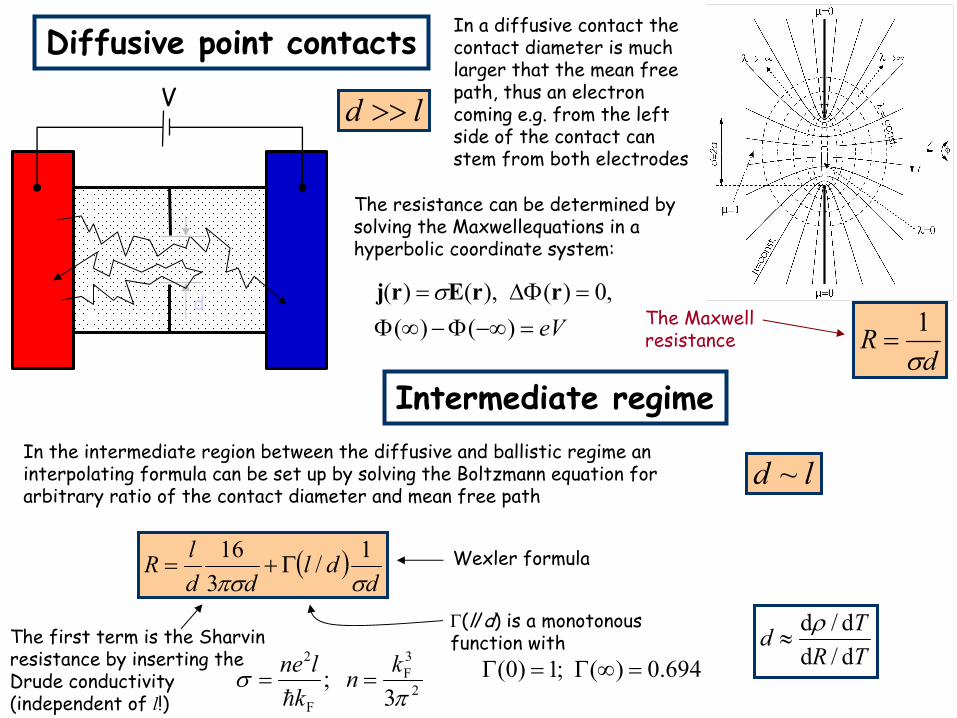
Diffusive point contacts
Intermediate regime
( )d
dldd
lRσπσ1/
316
Γ+=
ld >>
In a diffusive contact thecontact diameter is muchlarger that the mean freepath, thus an electroncoming e.g. from the leftside of the contact canstem from both electrodes
The resistance can be determined bysolving the Maxwellequations in a hyperbolic coordinate system:
The Maxwellresistance
In the intermediate region between the diffusive and ballistic regime aninterpolating formula can be set up by solving the Boltzmann equation forarbitrary ratio of the contact diameter and mean free path
ld ~
Wexler formula
The first term is the Sharvinresistance by inserting theDrude conductivity(independent of l!)
Γ(l/d) is a monotonousfunction with TR
Tdd/dd/dρ
≈
2
3F
F
2
3;
πσ kn
klne
==h
694.0)(;1)0( =∞Γ=Γ
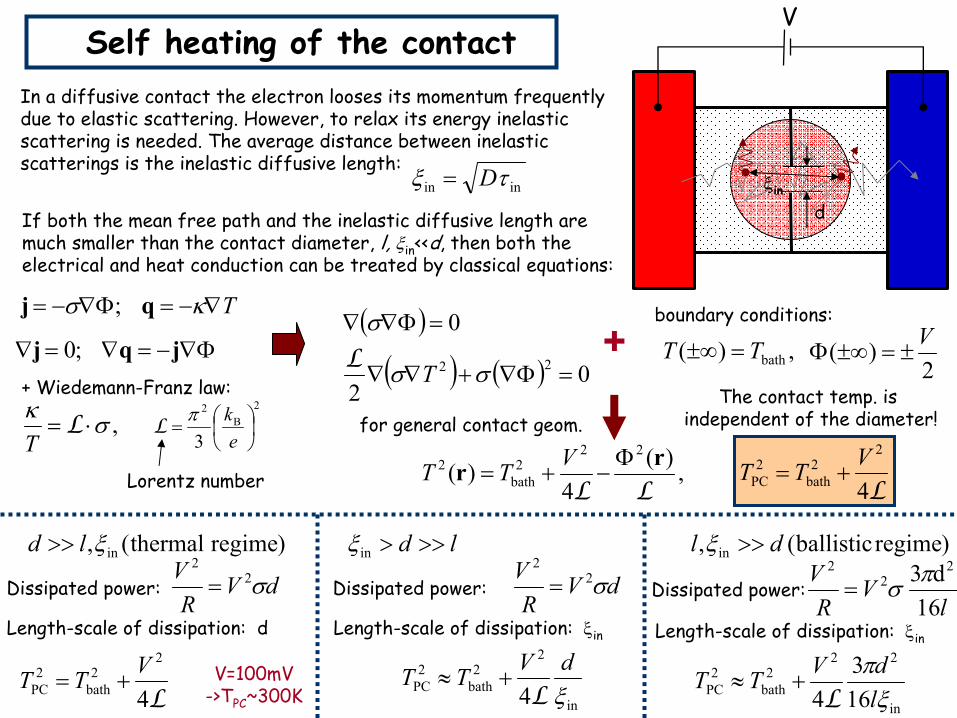
Self heating of the contact
T∇−=Φ∇−= κσ qj ;
2B
3
=
2
ekπL
Dissipated power:
,σκ⋅= L
T
+ Wiedemann-Franz law:
Lorentz number
If both the mean free path and the inelastic diffusive length aremuch smaller than the contact diameter, l, ξin<<d, then both theelectrical and heat conduction can be treated by classical equations:
Φ∇−=∇=∇ jqj ;0( )
( ) ( ) 02
022 =Φ∇+∇∇
=Φ∇∇
σσ
σ
TL
,)(4
)(22
2bath
2
LLrr Φ
−+=VTT
2)( V
±=±∞Φ,)( bathTT =±∞
L4
22
bath2
PCVTT +=
V
dξin
In a diffusive contact the electron looses its momentum frequentlydue to elastic scattering. However, to relax its energy inelasticscattering is needed. The average distance between inelasticscatterings is the inelastic diffusive length:
inin τξ D=
boundary conditions:
+
)regimethermal(, inξld >>
Length-scale of dissipation: d
L4
22
bath2
PCVTT +=
dVRV σ2
2
= Dissipated power:
ld >>>inξ
Length-scale of dissipation: ξin
in
22
bath2
PC 4 ξdVTT
L+≈
dVRV σ2
2
= Dissipated power:
)regimeballistic(, in dl >>ξ
Length-scale of dissipation: ξin
in
222
bath2
PC 163
4 ξπldVTT
L+≈
lV
RV
16d3 2
22 πσ=
The contact temp. is independent of the diameter!
V=100mV->TPC~300K
for general contact geom.
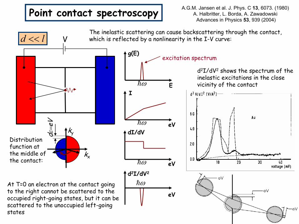
Distributionfunction atthe middle ofthe contact:
V
kx
kydε=e
V
Point contact spectroscopy
At T=0 an electron at the contact goingto the right cannot be scattered to theoccupied right-going states, but it can be scattered to the unoccupied left-goingstates
The inelastic scattering can cause backscattering through the contact,which is reflected by a nonlinearity in the I-V curve:ld <<
eV
eV
eV
dI/dV
d2I/dV2
IE
g(E)excitation spectrum
d2I/dV2 shows the spectrum of theinelastic excitations in the closevicinity of the contactωh
ωh
ωh
ωh
A.G.M. Jansen et al. J. Phys. C 13, 6073. (1980)A. Halbritter, L. Borda, A. Zawadowski
Advances in Physics 53, 939 (2004)
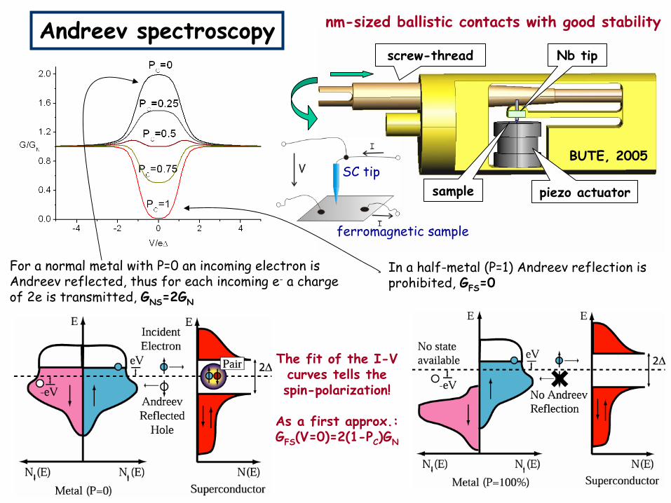
piezo actuator
screw-thread
sample
Nb tip
For a normal metal with P=0 an incoming electron isAndreev reflected, thus for each incoming e- a chargeof 2e is transmitted, GNS=2GN
The fit of the I-Vcurves tells thespin-polarization!
As a first approx.:GFS(V=0)=2(1-PC)GN
nm-sized ballistic contacts with good stabilityAndreev spectroscopy
In a half-metal (P=1) Andreev reflection is prohibited, GFS=0
BUTE, 2005SC tip
ferromagnetic sample
2 DEG
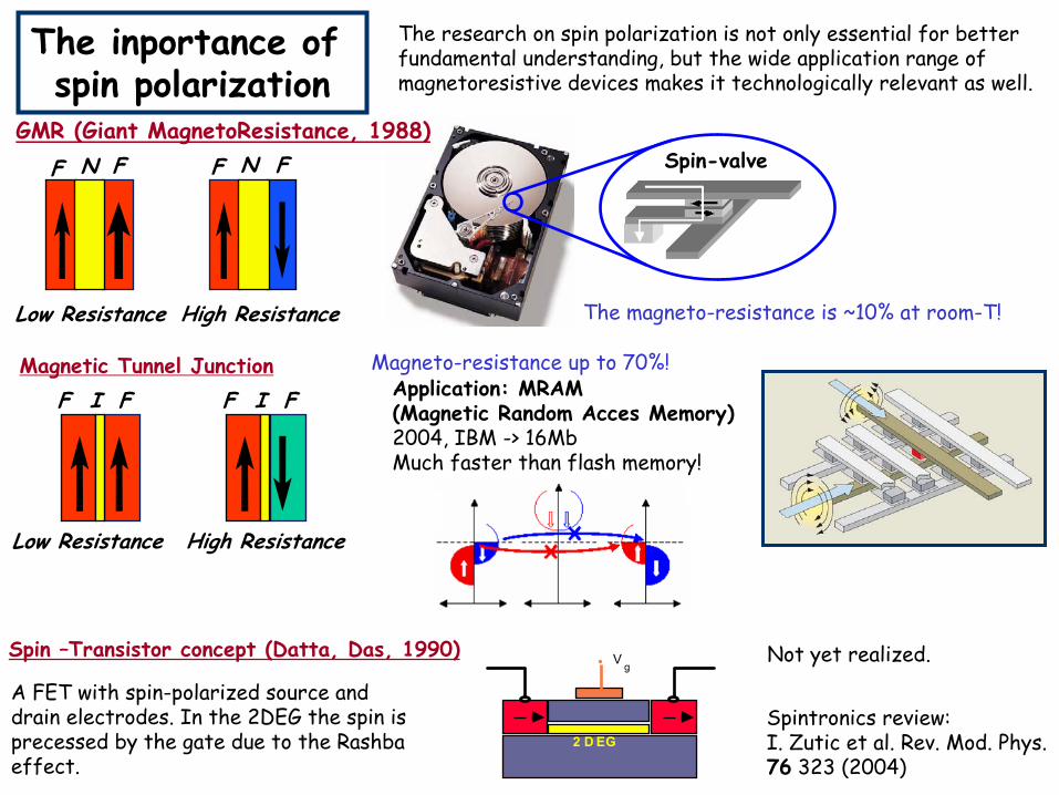
V gSpin –Transistor concept (Datta, Das, 1990)
Low Resistance
F N F
High
F N F
Low
High Resistance
F FI F FI
High ResistanceLow Resistance
Magnetic Tunnel Junction
The research on spin polarization is not only essential for better fundamental understanding, but the wide application range of magnetoresistive devices makes it technologically relevant as well.
The inportance ofspin polarization
Spin-valve
A FET with spin-polarized source anddrain electrodes. In the 2DEG the spin isprecessed by the gate due to the Rashbaeffect.
The magneto-resistance is ~10% at room-T!
GMR (Giant MagnetoResistance, 1988)
Application: MRAM (Magnetic Random Acces Memory)2004, IBM -> 16MbMuch faster than flash memory!
Magneto-resistance up to 70%!
Not yet realized.
Spintronics review:I. Zutic et al. Rev. Mod. Phys.76 323 (2004)
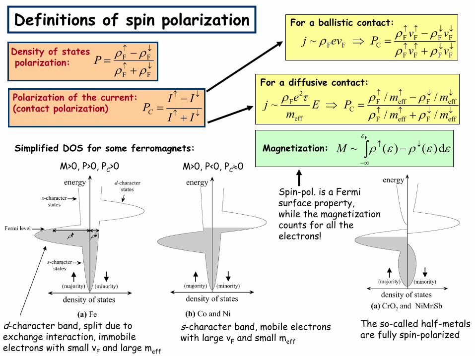
Definitions of spin polarization
↓↑
↓↑
+−
=FF
FF
ρρρρP
Density of statespolarization:
↓↑
↓↑
+
−=
IIII
PCPolarization of the current:(contact polarization)
For a ballistic contact:
↓↓↑↑
↓↓↑↑
+−
=⇒FFFF
FFFFCFF~
vvvvPevj
ρρρρρ
For a diffusive contact:
↓↓↑↑
↓↓↑↑
+−
=⇒effFeffF
effFeffFC
eff
2F
////~mmmmPE
mej
ρρρρτρ
Simplified DOS for some ferromagnets:
s-character band, mobile electronswith large vF and small meff
d-character band, split due toexchange interaction, immobileelectrons with small vF and large meff
The so-called half-metalsare fully spin-polarized
Spin-pol. is a Fermisurface property, while the magnetizationcounts for all theelectrons!
M>0, P>0, PC>0 M>0, P<0, PC≈0
Magnetization: εερερε
d~F
∫∞−
↓↑ )(−)(M
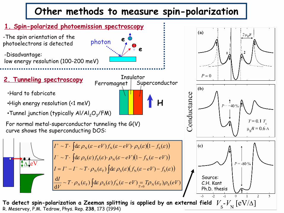
2. Tunneling spectroscopy
1. Spin-polarized photoemission spectroscopy
•Hard to fabricate
•High energy resolution (<1 meV)
•Tunnel junction (typically Al/Al2O3/FM)
eephoton
SuperconductorFerromagnet
H
Insulator
Other methods to measure spin-polarization
-Disadvantage: low energy resolution (100-200 meV)
-The spin orientation of the photoelectrons is detected
0=P
( )( )
( )
)()()()(d)(~dd
)()()(d)(~
)(1)()()(d~
)(1)()()(d~
SFN0
'NSFN
SNSFN
NNSS
SSNN
eVTeVfTVI
feVfTIII
eVfeVfTI
feVfeVTI
Tρερεερεερ
εεερεερ
εερεερε
εερεερε
=
−+
−
+
=−⋅
−−⋅−=
−−−⋅⋅
−⋅−−⋅
∫
∫∫∫
eV∆
For normal metal-superconductor tunneling the G(V)curve shows the superconducting DOS:
To detect spin-polarization a Zeeman splitting is applied by an external fieldR. Meservey, P.M. Tedrow, Phys. Rep. 238, 173 (1994)
Source:C.H. Kant Ph.D. thesis
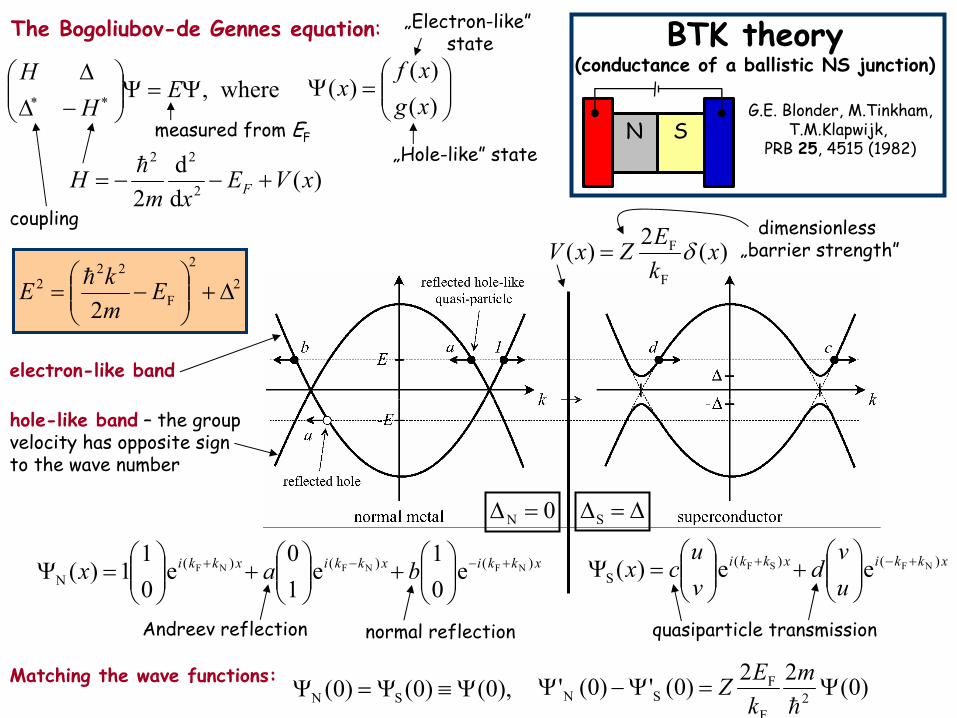
BTK theory(conductance of a ballistic NS junction)
where,Ψ=Ψ
−∆
∆∗∗ E
HH
=Ψ
)()(
)(xgxf
x
)(dd
2 2
22
xVExm
H F +−−=h
22
F
222
2∆+
−= E
mkE h
xkkixkkixkki bax )()()(N
NFNFNF e01
e10
e01
1)( +−−+
+
+
=Ψ xkkixkki
uv
dvu
cx )()(S
NFSF ee)( +−+
+
=Ψ
)(2)(F
F xkEZxV δ=
),0()0()0( SN Ψ≡Ψ=Ψ )0(22)0(')0(' 2F
FSN Ψ=Ψ−Ψ
h
mkEZ
„Electron-like”state
„Hole-like” state
The Bogoliubov-de Gennes equation:
measured from EF
dimensionless„barrier strength”
0N =∆ ∆=∆S
Andreev reflection normal reflection quasiparticle transmission
coupling
electron-like band
hole-like band – the groupvelocity has opposite signto the wave number
Matching the wave functions:
N SG.E. Blonder, M.Tinkham,
T.M.Klapwijk, PRB 25, 4515 (1982)
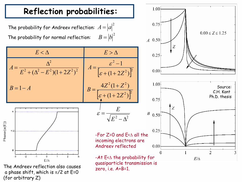
Reflection probabilities:
The probability for Andreev reflection:
The Andreev reflection also causesa phase shift, which is π/2 at E=0
(for arbitrary Z)
2aA =2bB =
22222
2
)21)(( ZEEA
+−∆+∆
=
[ ]22
22
)21()1(4
ZZZB
++
+=
ε
[ ]22
2
)21(1Z
A++
−=
εε
AB −=1
∆<E ∆>E
22 ∆−=
EEε
The probability for normal reflection:
-For Z=0 and E<∆ all theincoming electrons areAndreev reflected
-At E<∆ the probability forquasiparticle transmission iszero, i.e. A+B=1.
Source:C.H. Kant
Ph.D. thesis
0
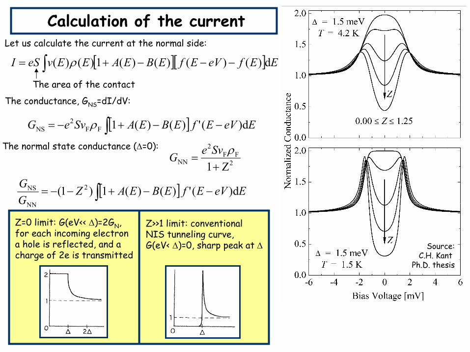
Calculation of the current
[ ][ ] EEfeVEfEBEAEEveSI d)()()()(1)()( −−−+= ∫ ρ
Let us calculate the current at the normal side:
The conductance, GNS=dI/dV:
The area of the contact
[ ] EeVEfEBEASveG d)(')()(1FF2
NS −−+−= ∫ρ
The normal state conductance (∆=0):2
FF2
NN Z1+=
ρSveG
[ ] EeVEfEBEAZGG d)(')()(1)1( 2
NN
NS −−+−−= ∫
Z>>1 limit: conventionalNIS tunneling curve, G(eV< ∆)=0, sharp peak at ∆
Z=0 limit: G(eV<< ∆)=2GN, for each incoming electrona hole is reflected, and a charge of 2e is transmitted
Source:C.H. Kant
Ph.D. thesis
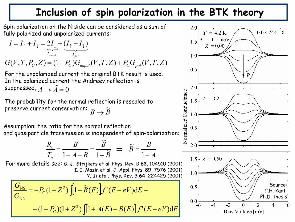
Inclusion of spin polarization in the BTK theorySpin polarization on the N side can be considered as a sum offully polarized and unpolarized currents:
BB ~→
2 ( )unpol polI I
I I I I I I↑ ↓ ↓ ↑ ↓= + = + −14243
( , , , ) (1 ) ( , , ) ( , , )C C unpol C polG V T P Z P G V T Z P G V T Z= − +For the unpolarized current the original BTK result is used. In the polarized current the Andreev reflection is suppressed,
The probability for the normal reflection is rescaled topreserve current conservation:
Assumption: the ratio for the normal reflectionand quasiparticle transmission is independent of spin-polarization:
ABB
BB
BAB
TR
n
n
−=⇒
−=
−−=
1~
~1
~
1
0~=→ AA
For more details see: G. J. Strijkers et al. Phys. Rev. B 63, 104510 (2001).I. I. Mazin et al. J. Appl. Phys. 89, 7576 (2001).
Y. Ji etal. Phys. Rev. B 64, 224425 (2001).
[ ][ ] EeVEfEBEAZP
EeVEfEBZPGG
d)(')()(1)1)(1(
d)(')(~1)1(
2C
2C
NN
NS
−−++−−
−−−−−=
∫
∫Source:
C.H. Kant Ph.D. thesis
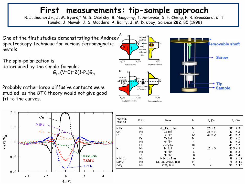
First measurements: tip-sample approachR. J. Soulen Jr., J. M. Byers,* M. S. Osofsky, B. Nadgorny, T. Ambrose, S. F. Cheng, P. R. Broussard, C. T.
Tanaka, J. Nowak, J. S. Moodera, A. Barry, J. M. D. Coey, Science 282, 85 (1998)
One of the first studies demonstrating the Andreevspectroscopy technique for various ferromagneticmetals.
The spin-polarization is determined by the simple formula:
GFS(V=0)=2(1-PC)GN
Probably rather large diffusive contacts werestudied, as the BTK theory would not give goodfit to the curves.
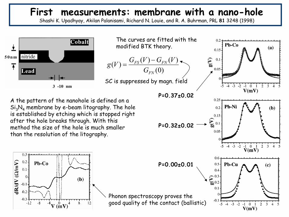
First measurements: membrane with a nano-holeShashi K. Upadhyay, Akilan Palanisami, Richard N. Louie, and R. A. Buhrman, PRL 81 3248 (1998)
A the pattern of the nanohole is defined on a Si3N4 membrane by e-beam litography. The holeis established by etching which is stopped rightafter the hole breaks through. With thismethod the size of the hole is much smallerthan the resolution of the litography.
Phonon spectroscopy proves thegood quality of the contact (ballistic)
The curves are fitted with themodified BTK theory.
P=0.37±0.02
P=0.32±0.02
P=0.00±0.01
)0()()()(
FN
FNFS
GVGVGVg −
=
SC is suppressed by magn. field
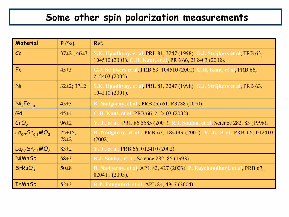
Some other spin polarization measurements
B. Nadgorny, et al, APL 82, 427 (2003). P. Raychaudhuri, et al, PRB 67, 020411 (2003).
50±8SrRuO3
R.J. Soulen, et al, Science 282, 85 (1998).58±3NiMnSb
R.P. Panguluri, et al, APL 84, 4947 (2004).52±3InMnSb
Y. Ji, et al, PRB 66, 012410 (2002).83±2La0.6Sr0.4MO3
B. Nadgorny, et al., PRB 63, 184433 (2001). Y. Ji, et al, PRB 66, 012410 (2002).
75±15; 78±2
La0.7Sr0.3MO3
Y. Ji, et al. PRL 86 5585 (2001). R.J. Soulen, et al, Science 282, 85 (1998).96±2CrO2
C.H. Kant, et al, PRB 66, 212403 (2002).45±4GdB. Nadgorny, et al., PRB (R) 61, R3788 (2000).45±3NixFe1-x
S.K. Upadhyay, et al, PRL 81, 3247 (1998). G.J. Strijkers et al, PRB 63, 104510 (2001).
32±2; 37±2Ni
G.J. Strijkers et al, PRB 63, 104510 (2001). C.H. Kant, et al, PRB 66, 212403 (2002).
45±3Fe
S.K. Upadhyay, et al, PRL 81, 3247 (1998). G.J. Strijkers et al, PRB 63, 104510 (2001). C.H. Kant, et al, PRB 66, 212403 (2002).
37±2 ; 46±3Co
Ref.P (%)Material
V
N S
V
N S
A
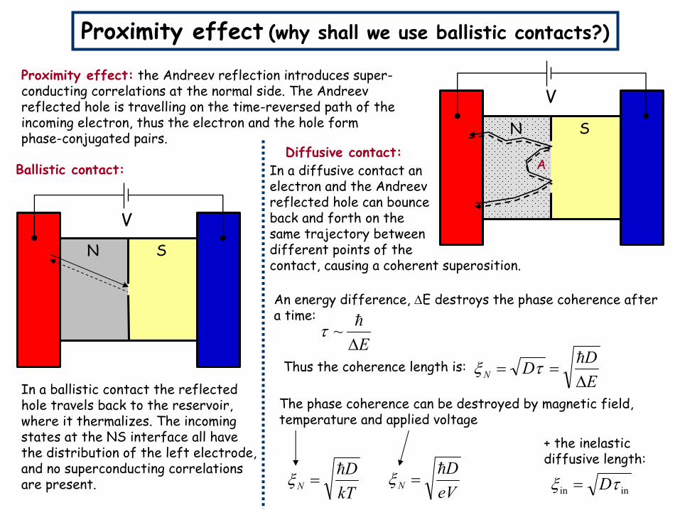
Proximity effect: the Andreev reflection introduces super-conducting correlations at the normal side. The Andreevreflected hole is travelling on the time-reversed path of theincoming electron, thus the electron and the hole formphase-conjugated pairs.
Proximity effect (why shall we use ballistic contacts?)
In a ballistic contact the reflectedhole travels back to the reservoir, where it thermalizes. The incomingstates at the NS interface all havethe distribution of the left electrode,and no superconducting correlationsare present.
Ballistic contact:Diffusive contact:
In a diffusive contact anelectron and the Andreevreflected hole can bounceback and forth on thesame trajectory betweendifferent points of thecontact, causing a coherent superosition.
An energy difference, ∆E destroys the phase coherence aftera time:
E∆h~τ
Thus the coherence length is:EDDN ∆
==hτξ
The phase coherence can be destroyed by magnetic field, temperature and applied voltage
kTD
Nh
=ξeVD
Nh
=ξ
+ the inelasticdiffusive length:
inin τξ D=
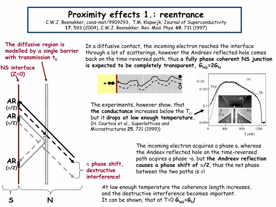
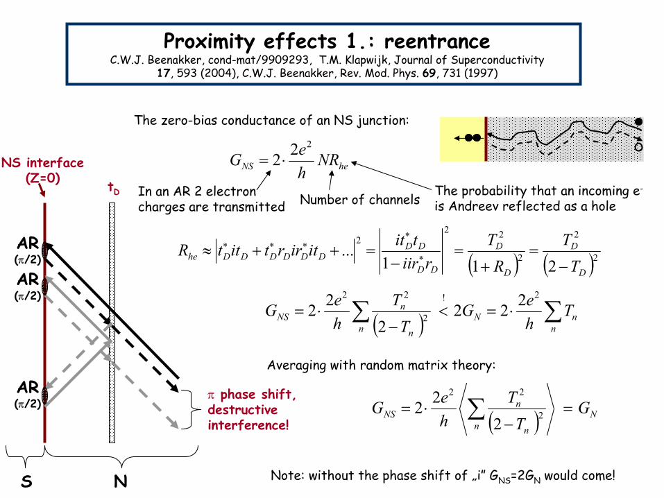
Proximity effects 1.: reentranceC.W.J. Beenakker, cond-mat/9909293, T.M. Klapwijk, Journal of Superconductivity
17, 593 (2004), C.W.J. Beenakker, Rev. Mod. Phys. 69, 731 (1997)
In a diffusive contact, the incoming electron reaches the interfacethrough a lot of scatterings, however the Andreev reflected hole comesback on the time-reversed path, thus a fully phase coherent NS junctionis expected to be completely transparent, GNS=2GN
The experiments, however show, thatthe conductance increases below the Tc,but it drops at low enough temperature.(H. Courtois et al., Superlattices andMicrostructures 25, 721 (1999))
The incoming electron acquires a phase φ, whereasthe Andeev reflected hole on the time-reversedpath acqires a phase –φ, but the Andreev reflectioncauses a phase shift of π/2, thus the net phasebetween the two paths is π!
At low enough temperature the coherence length increases,and the destructive interference becomes important. It can be shown, that at T=0 GNS=GN!
AR(π/2)
S N
NS interface(Z=0)
The diffusive region ismodelled by a single barrierwith transmission tD
π phase shift,destructiveinterference!
AR(π/2)
AR(π/2)
Proximity effects 1.: reentranceC.W.J. Beenakker, cond-mat/9909293, T.M. Klapwijk, Journal of Superconductivity
17, 593 (2004), C.W.J. Beenakker, Rev. Mod. Phys. 69, 731 (1997)
AR(π/2)
S N
NS interface(Z=0) tD
π phase shift,destructiveinterference!
AR(π/2)
AR(π/2)
The zero-bias conductance of an NS junction:
heNS NRheG
222 ⋅=
In an AR 2 electroncharges are transmitted Number of channels The probability that an incoming e-
is Andreev reflected as a hole
( ) ( )2
2
2
222
211...
D
D
D
D
DD
DDDDDDDDhe
TT
RT
riirtititirrtittR
−=
+=
−=++≈ ∗
∗∗∗∗
( ) ∑∑ ⋅=<−
⋅=n
nNn n
nNS T
heG
TT
heG
2!
2
22 2222
22
Averaging with random matrix theory:
( ) Nn n
nNS G
TT
heG =
−⋅= ∑ 2
22
222
Note: without the phase shift of „i” GNS=2GN would come!
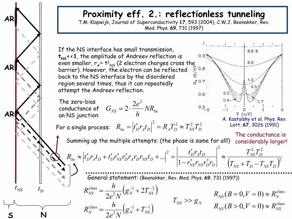
Proximity eff. 2.: reflectionless tunnelingT.M. Klapwijk, Journal of Superconductivity 17, 593 (2004), C.W.J. Beenakker, Rev.
Mod. Phys. 69, 731 (1997)AR
AR
AR
S N
If the NS interface has small transmission, tNS<<1, the amplitude of Andreev reflection is even smaller, rA~ t2
NS (2 electron charges cross thebarrier). However, the electron can be reflectedback to the NS interface by the disorderedregion several times, thus it can repeatedlyattempt the Andreev reflection.
The zero-biasconductance ofan NS junction:
heNS NRheG
222 ⋅=
For a single process: 2222
DNSDADADhe TTTRtrtR ≈== ∗
Summing up the multiple attempts: (the phase is same for all!)
A. Kastalsky et al. Phys. Rev.Lett. 67, 3026 (1991)
NSt Dt
( )2
2222
1...
DNSDNS
DNS
DDNSNS
DADDNSDADNSDDADhe
TTTTTT
rrrrtrttrrrrrttrtR
−+≈
−=++≈ ∗∗
∗∗∗∗∗
The conductance is considerably larger!
( )212
class 22
−− += NSNNS TgNehR
( )112
class
2−− += NSNN Tg
NehR
class
class
)0,0(
)0,0(
NSNS
NNS
RVBR
RVBR
≈=>
≈==NNS gT >>
General statement: (Beenakker, Rev. Mod. Phys. 69, 731 (1997))
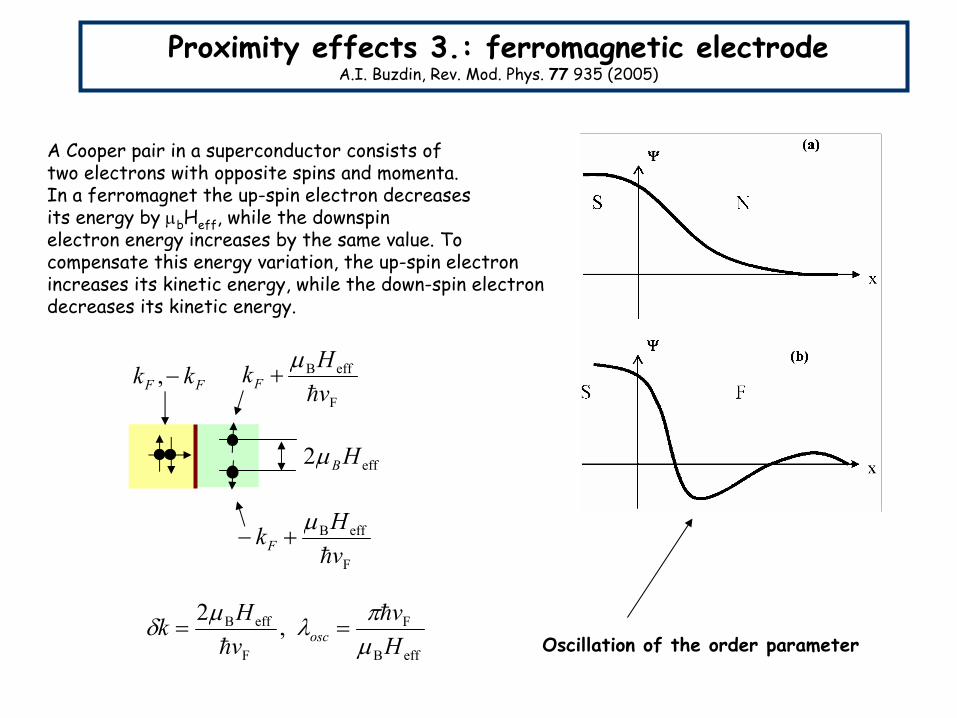
Proximity effects 3.: ferromagnetic electrodeA.I. Buzdin, Rev. Mod. Phys. 77 935 (2005)
eff2 HBµ
F
effB
vHkFh
µ+FF kk −,
F
effB
vHkFh
µ+−
effB
F
F
effB ,2Hv
vHk osc µ
πλµδ h
h==
A Cooper pair in a superconductor consists of two electrons with opposite spins and momenta. In a ferromagnet the up-spin electron decreases its energy by µbHeff, while the downspinelectron energy increases by the same value. Tocompensate this energy variation, the up-spin electronincreases its kinetic energy, while the down-spin electrondecreases its kinetic energy.
Oscillation of the order parameter
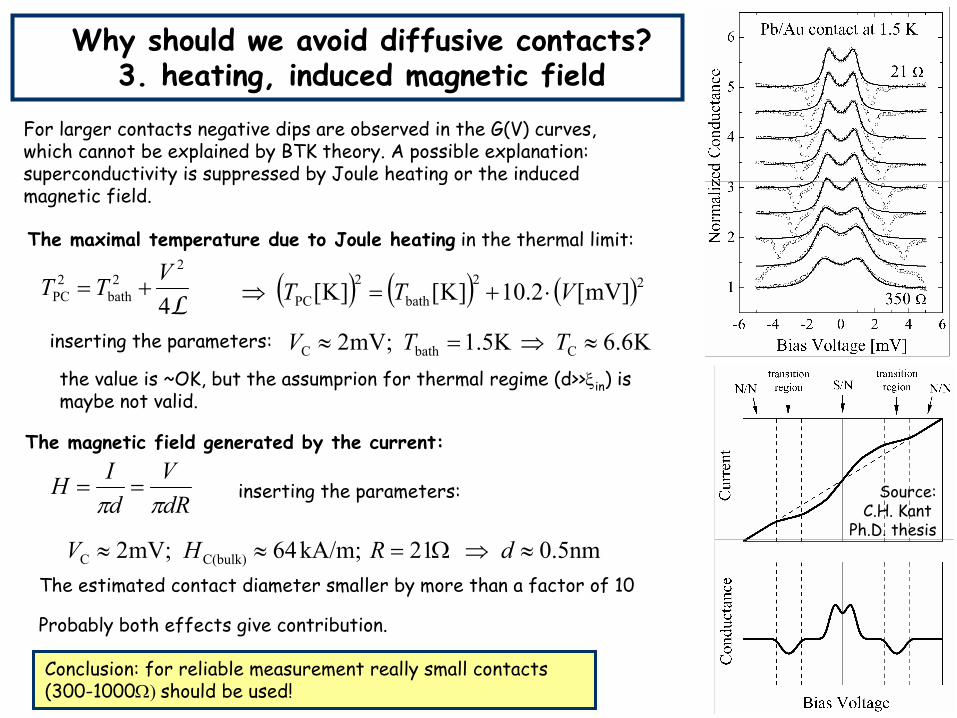
Why should we avoid diffusive contacts?3. heating, induced magnetic field
For larger contacts negative dips are observed in the G(V) curves,which cannot be explained by BTK theory. A possible explanation:superconductivity is suppressed by Joule heating or the inducedmagnetic field.
L4
22
bath2
PCVTT += ( ) ( ) ( )22
bath2
PC ]mV[2.10]K[]K[ VTT ⋅+=⇒
K6.6K 5.1mV;2 CbathC ≈⇒=≈ TTV
dRV
dIH
ππ==
nm5.0 21 kA/m;64mV;2 C(bulk)C ≈⇒Ω=≈≈ dRHV
The maximal temperature due to Joule heating in the thermal limit:
inserting the parameters:
the value is ~OK, but the assumprion for thermal regime (d>>ξin) is maybe not valid.
The magnetic field generated by the current:
inserting the parameters:
The estimated contact diameter smaller by more than a factor of 10
Probably both effects give contribution.
Conclusion: for reliable measurement really small contacts(300-1000Ω) should be used!
Source:C.H. Kant
Ph.D. thesis
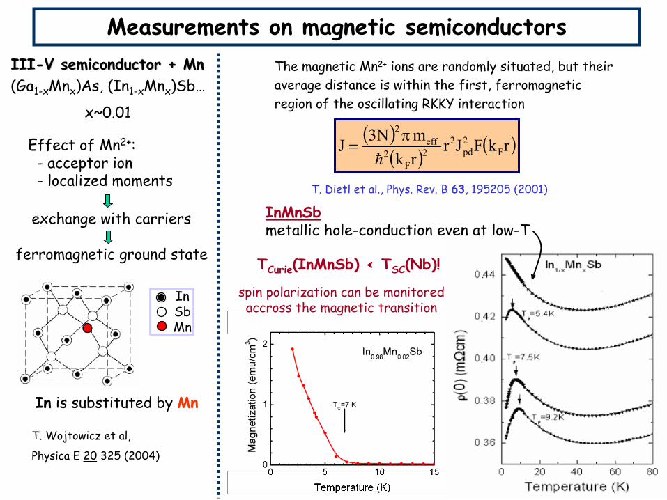
Measurements on magnetic semiconductors
Effect of Mn2+:- acceptor ion- localized moments
exchange with carriers
ferromagnetic ground state TCurie(InMnSb) < TSC(Nb)!
spin polarization can be monitoredaccross the magnetic transition
InSbMn
T. Wojtowicz et al,
Physica E 20 325 (2004)
( )( )
( )rkFJrrkmN3J F
2pd
22
F2
eff2
h
π=
T. Dietl et al., Phys. Rev. B 63, 195205 (2001)
The magnetic Mn2+ ions are randomly situated, but theiraverage distance is within the first, ferromagneticregion of the oscillating RKKY interaction
(Ga1-xMnx)As, (In1-xMnx)Sb…
x~0.01
IIIIII--V V semiconductorsemiconductor + + MnMn
In is substituted by Mn
InMnSbmetallic hole-conduction even at low-T
H. Ohno et al., Nature 408, 944(2000)
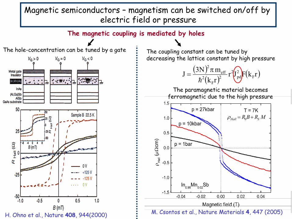
The magnetic coupling is mediated by holes
( )( )
( )rkFJrrkmN3J F
2pd
22
F2
eff2
h
π=
The paramagnetic material becomesferromagnetic due to the high pressure
MRBR SHall += 0ρ
M. Csontos et al., Nature Materials 4, 447 (2005)
Magnetic semiconductors – magnetism can be switched on/off byelectric field or pressure
The hole-concentration can be tuned by a gate The coupling constant can be tuned bydecreasing the lattice constant by high pressure
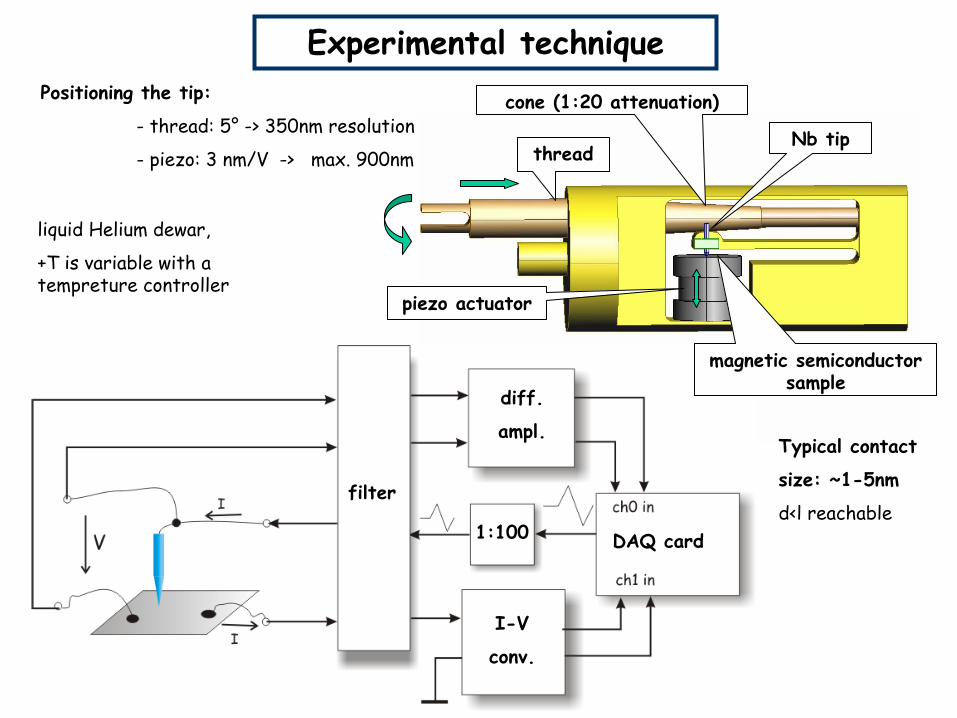
Nb tip
Typical contact
size: ~1-5nm
d<l reachable
Experimental technique
thread
piezo actuator
Positioning the tip:
- thread: 5° -> 350nm resolution
- piezo: 3 nm/V -> max. 900nm
cone (1:20 attenuation)
magnetic semiconductorsample
filter
diff.
ampl.
DAQ card1:100
I-V
conv.
liquid Helium dewar,
+T is variable with atempreture controller
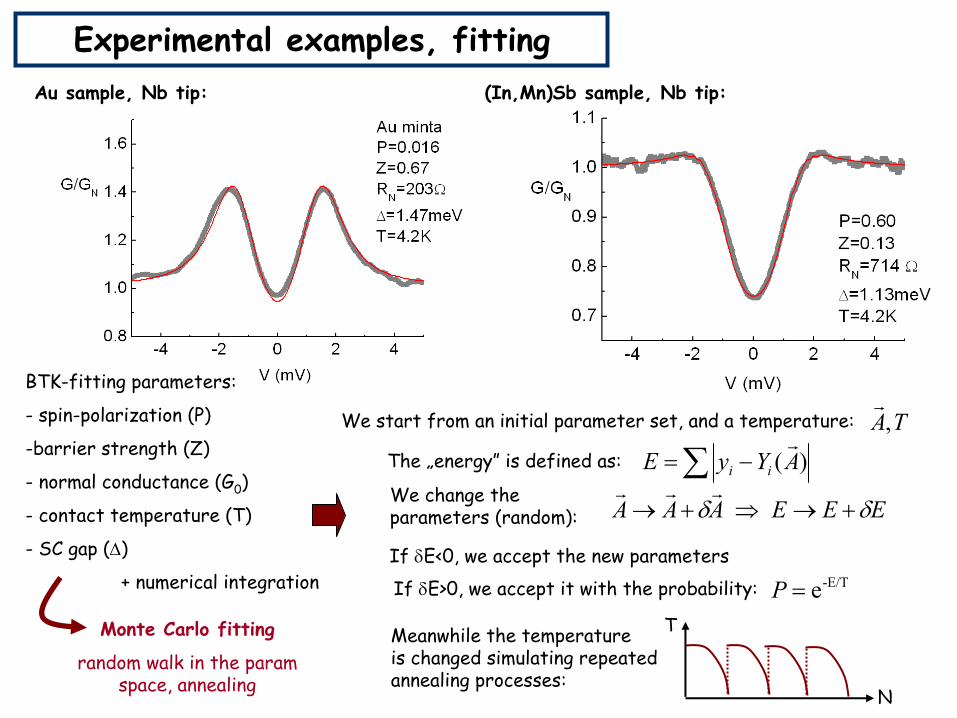
Au sample, Nb tip: (In,Mn)Sb sample, Nb tip:
Experimental examples, fitting
BTK-fitting parameters:
- spin-polarization (P)
-barrier strength (Z)
- normal conductance (G0)
- contact temperature (T)
- SC gap (∆)
+ numerical integration
Monte Carlo fitting
random walk in the paramspace, annealing
EEEAAA δδ +→⇒+→rrr
We start from an initial parameter set, and a temperature:
The „energy” is defined as: ∑ −= )(AYyE ii
r
We change theparameters (random):
If δE<0, we accept the new parametersIf δE>0, we accept it with the probability: -E/Te=P
TA,r
T
N
Meanwhile the temperatureis changed simulating repeatedannealing processes:
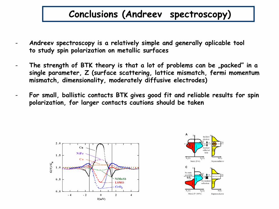
Conclusions (Andreev spectroscopy)
- Andreev spectroscopy is a relatively simple and generally aplicable toolto study spin polarization on metallic surfaces
- The strength of BTK theory is that a lot of problems can be „packed” in a single parameter, Z (surface scattering, lattice mismatch, fermi momentum mismatch, dimensionality, moderately diffusive electrodes)
- For small, ballistic contacts BTK gives good fit and reliable results for spin polarization, for larger contacts cautions should be taken