Andreas Stetter Conductivity of Multiwall Carbon Nanotubes: Role … · 2011-08-18 · Andreas...
95
Andreas Stetter Dissertationsreihe Physik - Band 21 Conductivity of Multiwall Carbon Nanotubes: Role of Multiple Shells and Defects Andreas Stetter 21 a 9 783868 450767 ISBN 978-3-86845-076-7 This work reports on laterally resolved measurements of the current-induced gradient in the electrochemical po- tential of multiwall carbon nanotubes. Nanotubes with different classes of defects were studied at room tem- perature. The potential profile of the outermost shell along the tube was measured in a local as well as in a nonlocal geometry. The data have been used to separate the contributions of various shells to the total resistance of the whole tube. For this purpose, a classical resistivity model was used that describes the measured potential profiles well. Additionally, the influence of structural defects on the conductivity has been quantified. Par- ticularly, defects such as an ending outermost shell, an intratube junction, and a plastically stretched tube with a kink were investigated. Additionally, measurements at low temperatures re- vealed some quantum conductance effects, such as weak localization and oscillations in the potential pro- file. The latter could be traced back to the same origin as the universal conductance fluctuations.
Transcript of Andreas Stetter Conductivity of Multiwall Carbon Nanotubes: Role … · 2011-08-18 · Andreas...

An
dre
as S
tett
erD
isse
rtat
ion
srei
he
Phys
ik -
Ban
d 2
1
Conductivity of MultiwallCarbon Nanotubes: Role ofMultiple Shells and Defects
Andreas Stetter
21a
9 783868 450767
ISBN 978-3-86845-076-7 ISBN 978-3-86845-076-7
This work reports on laterally resolved measurements of the current-induced gradient in the electrochemical po-tential of multiwall carbon nanotubes. Nanotubes with different classes of defects were studied at room tem-perature. The potential profile of the outermost shell along the tube was measured in a local as well as in a nonlocal geometry. The data have been used to separate the contributions of various shells to the total resistance of the whole tube. For this purpose, a classical resistivity model was used that describes the measured potential profiles well. Additionally, the influence of structural defects on the conductivity has been quantified. Par-ticularly, defects such as an ending outermost shell, an intratube junction, and a plastically stretched tube with a kink were investigated.Additionally, measurements at low temperatures re-vealed some quantum conductance effects, such as weak localization and oscillations in the potential pro-file. The latter could be traced back to the same origin as the universal conductance fluctuations.

Andreas Stetter
Conductivity of Multiwall Carbon Nanotubes: Role of Multiple Shells and Defects

Herausgegeben vom Präsidium des Alumnivereins der Physikalischen Fakultät:Klaus Richter, Andreas Schäfer, Werner Wegscheider, Dieter Weiss
Dissertationsreihe der Fakultät für Physik der Universität Regensburg, Band 21
Conductivity of Multiwall Carbon Nanotubes:Role of Multiple Shells and Defects
Dissertation zur Erlangung des Doktorgrades der Naturwissenschaften (Dr. rer. nat.)der Fakultät für Physik der Universität Regensburgvorgelegt von
Andreas Stetter
aus Regensburg2010
Die Arbeit wurde von Prof. Dr. C. H. Back angeleitet.Das Promotionsgesuch wurde am 29.10.2010 eingereicht.
Prüfungsausschuss:
1. Gutachter: Prof. Dr. C. H. Back 2. Gutachter: Prof. Dr. C. Strunk
Vorsitzende:
weiterer Prüfer:
Prof. Dr. M. Grifoni
Prof. Dr. R. Huber

Andreas Stetter
Conductivity of Multiwall Carbon Nanotubes: Role of Multiple Shells and defects

Bibliografische Informationen der Deutschen Bibliothek.Die Deutsche Bibliothek verzeichnet diese Publikationin der Deutschen Nationalbibliografie. Detailierte bibliografische Daten sind im Internet über http://dnb.ddb.de abrufbar.
1. Auflage 2011© 2011 Universitätsverlag, RegensburgLeibnizstraße 13, 93055 Regensburg
Konzeption: Thomas Geiger Umschlagentwurf: Franz Stadler, Designcooperative Nittenau eGLayout: Andreas Stetter Druck: Docupoint, MagdeburgISBN: 978-3-86845-076-7
Alle Rechte vorbehalten. Ohne ausdrückliche Genehmigung des Verlags ist es nicht gestattet, dieses Buch oder Teile daraus auf fototechnischem oder elektronischem Weg zu vervielfältigen.
Weitere Informationen zum Verlagsprogramm erhalten Sie unter:www.univerlag-regensburg.de

Conductivity of Multiwall CarbonNanotubes:
Role of Multiple Shells and Defects
Dissertationzur Erlangung des Doktorgrades der
Naturwissenschaften(Dr. rer. nat.)
der Fakultat Physik der UniversitatRegensburg
vorgelegt von
Andreas Stetteraus Regensburg
im Jahr 2010

Promotionsgesuch eingereicht am 29.10.2010Die Arbeit wurde angeleitet von: Prof. Dr. C. H. Back
Prufungsausschuss:Vorsitzende: Prof. Dr. M. Grifoni1. Gutachter: Prof. Dr. C. H. Back2. Gutachter: Prof. Dr. C. StrunkWeiterer Prufer: Prof. Dr. R. Huber

Contents
List of Figures VII
1 A History of carbon science 1
2 Carbon nanotubes: A one dimensional material 32.1 Structure of carbon nanotubes . . . . . . . . . . . . . . . . . . . . 3
2.1.1 Ideal carbon nanotubes . . . . . . . . . . . . . . . . . . . . 32.1.2 The reality: dirt and defects . . . . . . . . . . . . . . . . . 5
2.2 Bandstructure and density of states . . . . . . . . . . . . . . . . 82.2.1 Graphene: the basis for nanotubes . . . . . . . . . . . . . 82.2.2 Carbon nanotubes: graphene rolled up to a cylinder . . . . 8
2.3 Transport properties . . . . . . . . . . . . . . . . . . . . . . . . . 112.3.1 Quantum conductance . . . . . . . . . . . . . . . . . . . . 112.3.2 Conductance at room temperature . . . . . . . . . . . . . 132.3.3 The role of defects and multiple shells . . . . . . . . . . . 14
3 The resistance network model of a MWCNT 173.1 Punctual current injection in an infinitely long tube . . . . . . . . 17
3.1.1 Beyond the electrodes . . . . . . . . . . . . . . . . . . . . 183.1.2 Between the electrodes . . . . . . . . . . . . . . . . . . . . 193.1.3 Discussion . . . . . . . . . . . . . . . . . . . . . . . . . . . 20
3.2 Continuous current injection and finite tube length . . . . . . . . 213.2.1 Injection zone . . . . . . . . . . . . . . . . . . . . . . . . 223.2.2 Boundary conditions . . . . . . . . . . . . . . . . . . . . . 233.2.3 Discussion . . . . . . . . . . . . . . . . . . . . . . . . . . . 25
3.3 Comparison of both models . . . . . . . . . . . . . . . . . . . . . 27
4 Experimental Setup 294.1 Sample design . . . . . . . . . . . . . . . . . . . . . . . . . . . . . 304.2 Measurement setup . . . . . . . . . . . . . . . . . . . . . . . . . . 32
V

- VI - Contents
5 Results obtained at room temperature 375.1 Sample A: a multiwall carbon nanotube with no obvious defects . 385.2 Sample B: a multiwall carbon nanotube with an incomplete outer-
most shell . . . . . . . . . . . . . . . . . . . . . . . . . . . . . . . 455.3 Sample C: A tube with a strongly varying diameter . . . . . . . . 49
5.3.1 Characteristics without gate voltage . . . . . . . . . . . . . 495.3.2 Behavior with applied gate voltage . . . . . . . . . . . . . 52
5.4 Sample D: a stretched nanotube with a kink . . . . . . . . . . . . 53
6 Low temperature results 596.1 Measurements in local geometry . . . . . . . . . . . . . . . . . . . 606.2 Measurements in non-local geometry . . . . . . . . . . . . . . . . 63
7 Summary 69
Bibliography 71

List of Figures
2.1 Structure and chiral vector of carbon nanotubes . . . . . . . . . . 42.2 Defects in the hexagonal lattice . . . . . . . . . . . . . . . . . . . 52.3 Edge dislocation in a multiwall carbon nanotube . . . . . . . . . . 62.4 Bent Nanotubes . . . . . . . . . . . . . . . . . . . . . . . . . . . . 72.5 Energy level of σ and π bonds . . . . . . . . . . . . . . . . . . . . 72.6 π and σ band relative to the Fermi level . . . . . . . . . . . . . . 92.7 Band structure of graphene with allowed k vectors . . . . . . . . . 102.8 Dispersion relation and density of states . . . . . . . . . . . . . . 10
3.1 Resistor network of a double-wall nanotube . . . . . . . . . . . . . 183.2 Current leaving the region between the electrodes . . . . . . . . . 203.3 Current and Voltage versus x . . . . . . . . . . . . . . . . . . . . 213.4 Resistor model with injection zone . . . . . . . . . . . . . . . . . 223.5 Effect of ll on the current . . . . . . . . . . . . . . . . . . . . . . . 253.6 Current in the injection zone . . . . . . . . . . . . . . . . . . . . . 263.7 Effect of ll on the potential profile . . . . . . . . . . . . . . . . . . 273.8 Comparison of current and voltage with and without additional
electrode . . . . . . . . . . . . . . . . . . . . . . . . . . . . . . . . 28
4.1 Tunneling characteristics of the insulating layer . . . . . . . . . . 314.2 Schematic drawing of the sample . . . . . . . . . . . . . . . . . . 324.3 The UHV-Nanoprobe . . . . . . . . . . . . . . . . . . . . . . . . . 334.4 The measurement setup . . . . . . . . . . . . . . . . . . . . . . . 34
5.1 Carbon nanotube with and without electrodes . . . . . . . . . . . 385.2 STM image of the parts between and beyond the electrodes . . . . 395.3 Potential profile of sample A . . . . . . . . . . . . . . . . . . . . . 405.4 Influence of the tube length on the bending . . . . . . . . . . . . . 415.5 Comparison of the potential decrease in the inner and the outermost
shell . . . . . . . . . . . . . . . . . . . . . . . . . . . . . . . . . . 43
VII

- VIII - List of Figures
5.6 Illustration and measurement of a tube with incomplete outermostshell . . . . . . . . . . . . . . . . . . . . . . . . . . . . . . . . . . 46
5.7 Potential measurements for both current directions . . . . . . . . 475.8 Model with incomplete outermost shell . . . . . . . . . . . . . . . 485.9 SEM image of sample C with varying radius . . . . . . . . . . . . 505.10 Potential profile of sample C without applied gate voltage . . . . 515.11 Potential profiles of sample C with applied gate voltage . . . . . . 525.12 Dependency on the gate voltage at one position . . . . . . . . . . 525.13 Sample D before and after manipulation . . . . . . . . . . . . . . 535.14 Potential profile of sample D with kink . . . . . . . . . . . . . . . 545.15 Non-local potential profile of sample D . . . . . . . . . . . . . . . 57
6.1 Local low temperature potential profiles of sample D . . . . . . . 606.2 Conductivities of the three sectors as a function of temperature . 626.3 Non-local potential profile of sample D at T = 110 K . . . . . . . 646.4 Non-local potential profile of sample D at T = 28 K . . . . . . . . 646.5 Interference between different pathways . . . . . . . . . . . . . . . 68

1 A History of carbon science
For a long time, carbon in its elemental state had been thought to exist in onlythree configurations. In its amorphous state, e.g. in charcoal and coal, carboncontributed to early technology of mankind. Early metallurgy is hardly imaginablewithout the use of charcoal for heating and reducing metal ores. Later coal andits derivative coke along with new technology initiated the industrial revolution.Another application for amorphous carbon that is used since the antiquity iscarbon black, a pure form of soot. Soot will be even more interesting furtherbelow in this chapter.
A second form of elemental carbon is graphite. It was used for writing and drawingin form of a pencil as well as for crucibles for molten steel because of its heat resis-tance. Due to this, combined with the weak bond between single layers, graphiteis a good lubricant for components that have to withstand high temperatures.Graphite is a stack of hexagonal graphene layers (this name was proposed by ref.[1]) in AB configuration. In order to achieve the planar hexagonal lattice thecarbon atoms are sp2 hybridized, where the three σ-bonds connect the adjacentatoms in an angle of 120. The π-orbitals, however, combine to a charge cloudbelow and above the plain.
The third elemental form of carbon, diamond, was also known since the antiquitybut only used as jewelery for a long time. Since diamond is the hardest materialknown, its applications for tools are countless. Furthermore, the thermal conduc-tivity of diamond is about five times higher than that of silver, although it is aperfect electrical insulator. These extraordinary properties result from the hardσ-bonds between the sp3 hybridized carbon atoms in tetrahedral configuration.
1967 a fourth manifestation of carbon was described: Lonsdalite also called hexag-onal diamond [2]. It is created from graphite under high pressure and high temper-atures where the orbital hybridization changes from sp2 to sp3 while the hexagonalconfiguration is kept.
The next step in carbon science was in 1985 as Kroto et al. [3] synthesizedremarkably stable pure carbon molecules consisting of 60 atoms. They proposed
1

- 2 - CHAPTER 1. A HISTORY OF CARBON SCIENCE
a round structure with sp2 hybridized hexagons and pentagons, arranged similarlyto a football and called them Buckminsterfullerenes. Subsequently small closedcarbon nanostructures like C60 or C70 became a large domain in science oncethey could easily be produced. For this purpose Kratschmer et al. [4] vaporizedgraphite in an arc in helium atmosphere and washed the fullerenes out of theformed soot.
In 1991 Iijima [5], who had already investigated soot in a transmission electronmicroscope and found graphitized carbon nanoparticles ten years earlier took someof the junk from the cathode of such an arc arrangement and found long hollowfibers with several walls [6]. This multiwall carbon nanotubes (MWCNTs) wereformed of several spheric fullerenes cut in two and connected again with a rolledup layer of graphite (graphene), one inside the other like a Matryoshka doll. Inpractice, the caps have mostly much more complex structures. The nanotubesranged in length from a few tens of nm up to several µm and a diameter of 4 to30 nm. The innermost tubes had diameters of about 2 to 4 nm.
Soon two groups reported independently the synthesis of single-walled carbonnanotubes. One was again Iijima, this time together with Ichihashi [7], of NECand the other were Bethune et al. [8] from the IBM Research Division. Theyboth used a quite similar apparatus like for MWCNTs but contaminated their arcelectrodes with iron and cobalt, respectively. This was an important developmentin order to describe experiments with theory which is reliably for the more simplesingle-wall tubes. Further investigations led to additional synthesis methods likelaser vaporisation [9] or catalytic methods [10].
Eventually, three dimensional (diamond, graphite), one dimensional (carbon nan-otubes) and zero dimensional (spherical fullerenes) carbon structures were estab-lished. Two dimensional structures, however, were presumed virtually impossibledue to existing theorems [11]. 2004 Novoselov [12] surprised with preparing freestanding single layer graphene on insulating SiO2. One year later the predictionthat electrons behave like massless dirac fermions [13] has been confirmed [14, 15].Since then graphene has drawn at least as much attention in science as carbonnanotubes or fullerenes.

2 Carbon nanotubes: A onedimensional material
The first micrographs of multiwall carbon nanotubes were published in a Rus-sian journal [16], nearly forty years before the modern nanotube research wastriggered by Iijima [6] in 1991. The high resolution transmission electron micro-graphs (TEM) of Iijima are nevertheless the first ones that revealed the multipleshell configuration of the multiwall carbon nanotubes (MWCNT).
2.1 Structure of carbon nanotubes
2.1.1 Ideal carbon nanotubes
The structure of a single-wall carbon nanotube (SWCNT) is easy imaginable bycutting a rectangle out of a graphene sheet and connecting two sides of it byrolling it up to a hollow cylinder. The connection condition of the crystal latticeallows only rectangles with the same configuration on two opposing sides. Foreasier notation the chiral vector ~Ch was adopted (see upper left of fig. 2.1), thatcorresponds to the circumference of the tube. If m = 0 (Θ = 0) it results azigzag tube and for n = m (Θ = 30) it results an armchair tube referring tothe structure along the circumference. All other combinations result in so-calledchiral tubes (illustrations in fig. 2.1. To saturate the dangling bonds on the endof the tube they are capped with an attached hemispherical fullerene. Since thecircumference is the absolute value of ~Ch, the diameter can be calculated to:
dT =
∣∣∣ ~Ch∣∣∣π
= a
π
√n2 + nm+m2 (2.1)
where a = 4.46 A is the lattice constant of the graphene honeycomb structure.
The diameters of real single-wall carbon nanotubes spread from about 0.4 nm [18]
3

- 4 - CHAPTER 2. CARBON NANOTUBES: A ONE DIMENSIONAL MATERIAL
Figure 2.1: The chiral vector ~Ch = n~a1 + m~a2 (see upper left part of the image)points from one K-point to an equivalent one of another cell. If one moves aninteger number n of lattice vector ~a1 and m of vector ~a2 (in this example 4 and 2,respectively) this condition is fulfilled. The angle between the two lattice vectors~a1 and ~a2 is 60. Θ is the chiral angle and (n,m) are the chiral indices. The sheet isjoined along ~T that has the direction axial to the tube. The other parts illustratethe structures of zig-zag, armchair and chiral tubes [17].

CHAPTER 2. CARBON NANOTUBES: A ONE DIMENSIONAL MATERIAL - 5 -
Figure 2.2: (a) Graphene fragment containing a vacancy. The carbon networkexhibits some reconstruction. (b) Graphene lattice with a Stone-Wales defect. (c)Nanotube doped with Nitrogen. Adapted from [24] ((a) and (b)) and [25] ((c)).
up to 6 nm (e.g.[19, 20]). Above this diameter SWCNTs are predicted to collapse[21]. Generally the chiral angles are evenly distributed [22].
Multiwall carbon nanotubes consist of several shells each of them looking like asingle-wall nanotube. The differences in the radii are in the range of 0.34 nm,similar to the interlayer distance in graphite [6]. Due to the difference in thediameters and therefore also to the different chiral vector, the individual layersare incommensurate. So the stacking of the layers differs necessarily from that ofgraphite whereby many attributes like interlayer conductance is not comparableanymore.
2.1.2 The reality: dirt and defects
Nowadays three techniques dominate CNT production: chemical vapor deposition[10], arc discharge [6] and laser ablation [9]. Although big progress has beenmade in this area, CNTs always appear together with amorphous soot and othercarbonaceous contamination. Additionally, for singe-wall tubes a metallic catalystis needed, that also gives rise to metallic impurities or to a compound of metal withcarbon. Since for technical or scientific applications clean nanotubes are desirable,purification methods are needed. These range from chemical oxidation, filtrationand centrifugation to solubilization with functional groups and annealing. For anoverview see ref. [23].
Just as the environment of as-grown nanotubes is not perfect so are the tubesthemselves. For single-wall nanotubes there are mainly defects in the hexagonallattice like vacancy, substitution of carbon atoms or including heptagons and pen-tagons in the lattice (fig. 2.2). One of the most common defects is the Stone-Wales

- 6 - CHAPTER 2. CARBON NANOTUBES: A ONE DIMENSIONAL MATERIAL
Figure 2.3: Edge dislocation in amultiwall carbon nanotube. Thisshould be a change-over from anested to a scrolled nanotube.Adapted from [29]
defect [26], where only one covalent bond rotates with 90, and two pentagons aswell as two heptagons are generated from the original hexagonal structure. Gen-erally, individual pentagons or heptagons introduce convex and concave bendingof the tube, respectively. Furthermore heptagons and pentagons can allow a con-nection between tubes with different diameters and chirality [27].
In multiwall carbon nanotubes additional defects due to interlayer effects canappear. In high resolution TEM images of MWCNTs it was quite often observedthat the distances between the fringes on both sides of the tube differ from eachother. Consequently the interlayer distance cannot be constant. Liuand et al. [28]observed a polygonal cross section and suggested the existence of several near-planar regions. These are joined together along lines of small radius of curvature.It was debated if the stacking in the planar regions is similar to graphite.
Especially the inner structures of MWCNTs can vary significantly. There can beone or more layers traversing the central core. Sometimes even closed compart-ments are seen [30]. Edge dislocations, for example, are defects affecting all shells.At this defect on one side of the tube the outermost shell is connected with the sec-ond outer shell and so on (fig. 2.3). It was discussed that this defect can representa change-over from a nested (as described above) to a scroll type nanotube1 [29].Intershell connections can also be induced artificially by breaking bonds via ozoneexposure. The atoms rearrange creating sp3 orbitals and cross-link the shells [31].This may lead to a increased transmission probability between the shells.
The Stone-Wales defects may also be induced by mechanical strain [32, 33]. Apply-ing additional strain and depending on chirality and temperature, the heptagons1Although it is not easy to distinguish a nested from a scroll type nanotube with TEM, thereare several indications that the nested structure is at least the more common: HR-TEM imagesshow the same number of shells on both sides. The observed caps and internal closed compart-ments are difficult to explain in a scroll structure; at least reactive gases attack the cap regionpreferentially, i.e. the tube itself has no specific area of attack.

CHAPTER 2. CARBON NANOTUBES: A ONE DIMENSIONAL MATERIAL - 7 -
Figure 2.4: HR-TEM images of slightly bent (left) (adapted from [38]) andstrongly bent (right) nanotubes (adapted from [39]).
Figure 2.5: The σ-bonds connectthe carbon atoms to the charac-teristic hexagonal lattice and areresponsible for the binding energyand the elastic properties (left).The corresponding bands are sep-arated by a large energy gap,whereas the energy level of the πorbitals lies around the Fermi levelEF (right). Adapted from [40]
and pentagons can diverge, again via bond rotations, moving around and alongthe tube leaving a slightly thinner tube with another chirality [33, 34]. Othertubes can become brittle due to many heptagon, pentagon or octagon defects [34],or the molecular bonds can fracture individually [35]. Especially for multiwalltubes there is another possibility to release the strain: individual tubes can breakat different positions and the whole tube can be extended telescopically [36, 37].
Another possibility to get a kink, besides including heptagons or pentagons whilegrowing is bending the originally ideal nanotube with mechanical force. Theresulting structure depends on the radius of curvature. Generally, the structureof the outer side remains flat, while the inner side buckles. Examples for slightlyand strongly bent tubes are given in fig. 2.4.

- 8 - CHAPTER 2. CARBON NANOTUBES: A ONE DIMENSIONAL MATERIAL
2.2 Bandstructure and density of states
2.2.1 Graphene: the basis for nanotubes
In all graphene based structures (graphite, fullerenes and carbon nanotubes) the2s, 2px and 2py orbitals hybridize to three sp2 hybrid orbitals with an includedangle of 120. These form together with their nearest neighbors covalent σ-bondsand combine to bonding σ and antibonding σ∗ molecular orbitals. The remaining2pz orbitals, perpendicular to the plane of the σ bonds, couple with their neighborsand form delocalized bonding π or antibonding π∗ orbitals above and below theplane. They are responsible for the weak interaction between graphene layers ingraphite [41], between several shells in MWCNTs or between individual tubes ina bundle of SWCNTs.The energy levels associated with the σ-bonds are far away from the Fermi leveland therefore they are irrelevant for their electronic properties (fig. 2.5). Incontrast, the π bands lie in the vicinity of the Fermi energy and therefore areresponsible for electronic behavior. In the vertex of the first Brillouin zone (theK or K′ point1) the π bands actually cross the Fermi level (fig. 2.6), which makesgraphene a semimetal. Furthermore in the vicinity of the K point the π bands arenearly linear.
2.2.2 Carbon nanotubes: graphene rolled up to a cylinder
A carbon nanotube results from a graphene sheet rolled up to a cylinder, conse-quently it exhibits a similar band structure. In the case of nanotubes only oneadditional constraint has to be fulfilled: going once around the circumference onegets to the same point, i.e. an additional boundary condition for the part of thewave vector k perpendicular to the tube axis exists:
Ψk(r + Ch) = Ψk(r) (2.2)
Due to the Bloch theorem there is a periodic function uk(r) = uk(r + Ch) with
Ψk(r) = eik · ruk(r) (2.3)Ψk(r + Ch) = eik · reik · Chuk(r + Ch) = eik · reik · Chuk(r) (2.4)
1only two (neighboring) of the six vertices in the first Brillouin zone are different, all others areequivalent to one of these two. Descriptively spoken it can be stated that only a third of everyvertex is in the first Brillouin zone and two thirds are outside.

CHAPTER 2. CARBON NANOTUBES: A ONE DIMENSIONAL MATERIAL - 9 -
Figure 2.6: Left: the band structure of graphene calculated from the tight-bindingmodel [42] results in the bonding π bands (below the Fermi level) and the anti-bonding π∗ bands (above the Fermi level). The bands touch only at K and K′ theFermi surface. Right: The bandstructure shows the large band gap between theσ and the σ∗ bands. The Fermi energy is set to zero, and Φ indicates the workfunction. Adapted from [24]
Comparing equation 2.2 with 2.3 and 2.4 results in the condition eik · Ch = 1 or
k · Ch = 2bπ with b ∈ Z (2.5)
This means that only k vectors are allowed that lie on a line through the Γ pointin tube direction and parallel in distances of b 2π
Ch. Plotting these allowed lines
in the band structure of graphene (fig. 2.6) results in the band structure for thenanotube (see fig. 2.7). If one of the allowed lines hits the K point, where valenceand conduction band are touching each other, the tube is metallic and if all linesmiss the K points there is a band gap: the tube is semiconducting. All armchairnanotubes are metallic because the line through Γ hits K and the opposite K′(b = 0). Generally, the tubes are metallic if n − m = 3l, l ∈ Z is fulfilled.All others are semiconducting. As in metallic tubes K and K′ are interceptedsimultaneously1, there are two conduction channels. Because the distance of thelines decreases with increasing diameter and the band structure around the Kpoint is linear, the band gap decreases, too.
The band structure of the carbon nanotubes is one dimensional like the tubeitself. It can be derived from that of graphene and the allowed k vectors by asuperposition of the energy dispersions along the lines. The centric line represents1If a line hits the K point, there is also one hitting K′ (b→ −b)

- 10 - CHAPTER 2. CARBON NANOTUBES: A ONE DIMENSIONAL MATERIAL
Figure 2.7: Band structure of graphene(calculated from the tight-bindingmodel [42]) together with the energy ofthe allowed wave vectors (solid lines)for an armchair nanotube. The centricline hits K and K′. The tube is metallic.
Figure 2.8: Dispersion relation and density of states of a metallic (5,5) armchairnanotube (left) and a semiconducting (10,0) zigzag tube (right). The extremawith horizontal tangents in the band structure result in a diverging density ofstates (van Hove singularity). γ0 ≈ 2.9 eV. The Γ-X direction is axial to thetube. Adapted from [24]
a propagating wave directly in tube direction, the other branches correspond toa helical propagation around the tube. Fig. 2.8 shows the band structure for ametallic (5,5) and a semiconducting (10,0) nanotube.
In a one dimensional system the density of states ρ(E) = dN(E)dE with dE = ∂E
∂kdk
can be written asρ(E) = dN
dk1∂E∂k
(2.6)
Consequently if dEdk = 0 (horizontal tangents in the band structure) the density
of states diverges (fig. 2.8). This is known as a van Hove singularity [43]. Fora metallic nanotube the density of states is constant in the vicinity of the Fermilevel.

CHAPTER 2. CARBON NANOTUBES: A ONE DIMENSIONAL MATERIAL - 11 -
All these calculations do not take into account that the graphene sheet is bentinto a nanotube. It was predicted, that especially in small diameter tubes withhigh curvature a small band gap up to about 10 meV appears in all tubes exceptarmchair tubes [44, 45]. This effect was measured by Ouyang et al. [46] in 2001.Even in the highly symmetric armchair nanotubes a small band gap occurs if thetube is in a bundle, due to the intertube interactions [47].
2.3 Transport properties
Although it took a rather long time since the discovery of carbon nanotubes 1991[6] to the first electrical resistance measurement of an individual carbon nanotube1996 [48], some transport properties like magnetoresistance were already knownfrom measurements on bundles of nanotubes [49, 50].
2.3.1 Quantum conductance
In a macroscopic material the resistivity is a material constant and independentof the geometry. In mesoscopic systems for dimensions in the range of the meanfree path Lm or of the phase coherence length Lϕ, however, quantum conductanceeffects appear. If the length of the contacted nanotube L becomes smaller thanboth, the mean free path and the phase coherence length, the intrinsic resistanceis independent of L. In this regime of ballistic transport there is not one Fermienergy EF defined, but two chemical potentials µl for the k vectors from leftto right and µr for the oposite direction, equal to the Fermi energy of the leftand right electrode, respectively. The conductance is G = M 2e2
h= MG0 where
M is the number of bands with electronic states between µl and µr [51]. Incarbon nanotubes with the Fermi energy at the charge neutrality point1 and lowbias the number of channels is M = 2, according to the touching valence andconductance bands on K and K′. In the clean limit with no scattering in thetube only the electrodes can disturb the wave propagation because of non idealcontacts (tunneling) or backscattering. For disordered or multiwalled tubes Lmas a function of the Fermi level was calculated [52, 53] and measured [54].
Several groups reported ballistic transport in MWCNTs for tube lengths up toseveral µm even at room temperature [55–59]. Surprisingly the early experimentsof Frank et al. [55] revealed a quantum conductance of only G = 1 G0. Subsequent1the energy level where π and π∗ crosses

- 12 - CHAPTER 2. CARBON NANOTUBES: A ONE DIMENSIONAL MATERIAL
experiments measured the predicted value of G = 2 G0 [56] but also a conductanceup to G = 490 G0 [57]. In all these experiments the nanotubes were grown directlyon one of the electrodes. In single-wall tubes also ballistic transport was reportedeven between evaporated electrodes, measured with an electric force microscope(EFM) [60].
In the more common contacting method with evaporated contacts, diffusive trans-port was reported for MWCNTs [48, 54, 60–65], but showing several quantumconductance effects.
Conductance measurements in a magnetic field can identify and distinguish weaklocalization, universal quantum fluctuations and Altshuler-Aronov-Spivac oscilla-tions. If Lm << Lϕ there are many scattering centers conserving phase coherence.Closed paths containing only phase coherent scatterers can be passed in both di-rections. Since the path and the phase of both parts of the wave is equal theyinterfere constructively. The increased probability of presence after passing theclosed path is equivalent to an increased probability of backscattering. The elec-tron mobility is decreased and therefore also the conductivity decreases. This isknown as weak localization. At low temperatures the phase destroying electron-phonon and electron-electron scattering events are reduced and the resistance isincreased due to weak localization.
Applying a magnetic field perpendicular to the closed path adds (subtracts) aphase difference to the two parts of the wave and destroys the constructive in-terference. A magnetoresistance peak at zero field indicates a weak localizationregime. Depending on the tube and the distribution of the scattering centersthere are additional smaller peaks in the magnetoresistance known as universalconductance fluctuations. They originate from interference effects between differ-ent paths. A magnetic field changes the phase relations between different pathsand leads to randomly distributed but reproducible oscillations. Weak localizationand universal conductance fluctuations were observed e.g. in refs. [54, 65, 66].
If the magnetic field is applied parallel to the tube only phases of paths going atleast once around the tube are altered. Since the phase difference depends linearlyon the enclosed flux and all paths once around the tube include the same flux, thereare periodic positions in the magnetic field where interference is constructive andtherefore the conductance is reduced [67]. In 1999 these oscillations were observedin multiwall tubes, since the required magnetic fields are only achievable for largediameter tubes [68]. Additionally this experiment showed that only the outershells with large diameter contribute to the current at low temperature.

CHAPTER 2. CARBON NANOTUBES: A ONE DIMENSIONAL MATERIAL - 13 -
In the case of weakly coupled electrodes i.e. high contact resistance, Coulombblockade dominates electronic transport [69, 70]. This effect originates from thecharging energy when one electron is added to the tube and suppresses conduc-tance if no energy level lies between the voltages on the electrodes. It was alsoreported that prestructured electrodes divide one single nanotube in several quan-tum dots due to bending near the edges of electrodes [71].Other quantum conductance effects like negative four point resistance [72] thatoriginate from backscattering effects at impurities and subsequent interference ofmultiply reflected waves, or Luttinger-liquid behavior [73] have been reported.
2.3.2 Conductance at room temperature
The described quantum conductance effects occur (except ballistic transport withtubes grown on the electrodes) only at low temperatures. For higher temperaturesup to room temperature the results for multiwall and single-wall nanotubes differstrongly. With EFM measurements Bachtold et al. [60] found clear evidence fordiffusive transport in a MWCNT and with the same setup no intrinsic resistancein metallic SWCNTs. For semiconducting SWCNTs, however, defects in the tubesdominated electron transport.An interesting experimental setup was used by Yaish et al. [62]. The authorshave injected current in a SWCNT using evaporated Au contacts and used theconducting tip of an atomic force microscope (AFM) as a local voltage probe. Inthis way the contact resistances could easily be measured directly to be 15 kΩindependent of the gate voltage. However, the potential drop near the electrodesdepended strongly on the gate voltage. Their results idicated that the Au contactsinduce Schottky barriers in n-type semiconducting tubes as observed in previousexperiments [74, 75]. On the other hand the potential drop away from the contactelectrodes was linear indicating diffusive transport for distances of at least 200 nm.Nonlinear resistance versus length was found by Pablo et al. [61] also with a con-ductive AFM but only in a two point setup with one evaporated electrode andthe other provided by the AFM tip. The authors conclude that this is due to thepresence of nondissipative scattering centers and that electron transport is coher-ent even for tubes with high intrinsic resistances. But it is also necessary to thinkabout possible Schottky barriers at the electrodes that result in an unexpectedscaling behavior [74].An experiment similar to that of Yaish et al. [62] but with even less invasivevoltage electrodes was carried out by Gao et al. [72]. They used two MWCNTs as

- 14 - CHAPTER 2. CARBON NANOTUBES: A ONE DIMENSIONAL MATERIAL
voltage probes in a four point setup and moved them with an AFM tip in order tomeasure the four point resistances for different lengths. At room temperature theyfound the resistance to be linear with distance, indicating a diffusive incoherentlimit. Additionally the four point resistance remains constant at temperaturesabove 80K, suggesting that the intrinsic resistance is due to disorder and not tophonon scattering. Other groups found contrarily a domination of electron-phononscattering at room temperature [65, 76–78].
2.3.3 The role of defects and multiple shells
The discrepancy in the results described above are on the one hand due to dif-ferences in tube diameter and chirality but on the other hand definitely due todifferences in the quality of the nanotube material. An often practiced methodto visualize defects is scanning gate microscopy (SGM). Here a charged AFM tipis scanned over the sample at constant height as a local gate and the the twopoint resistance is recorded as a function of the the tip position. Since defectsin nanotubes have a large impact on the conductance a local change in Fermienergy at a defect alters the conductance much more than at other positions. Itwas found, that especially in semiconducting tubes voltage drop occurs mainly atdefects [60, 79]. Since in MWCNTs the shells are typically incommensurate theyintroduce an aperiodic potential that can be handled as a defect density [80], theSGM detects defects all over the tube. Therefore this method is not as effectiveas in SWCNTs.From a theoretical point of view defects can be handled with a disorder parameterthat is constant over the whole tube as it was done by Triozon et al. [52]. Theresult was a diffusive transport with Lm scaling with the tube diameter and beingstrongly dependent on the Fermi level. At least the latter has been confirmedexperimentally by Stojetz et al. [54].Alternatively, individual defects can be modeled and their impact on the densityof states or transmission probability can be calculated. This was performed forexample by Rochefort et al. [81] with bent nanotubes and a strong decrease intransmission probability due to σ-π hybridization effects was found. Other groupsreported a decrease of the density of states in bent nanotubes [82]. Strain alsoreduces the density of states [83].A lot of experimental work was done in characterizing the electronic behavior ofcarbon nanotubes with defects. Bending multiwall nanotubes, measuring theirresistance and simultaneously recording TEM images of the defects revealed that

CHAPTER 2. CARBON NANOTUBES: A ONE DIMENSIONAL MATERIAL - 15 -
conductance decreases with curvature and stronger bendings result in plastic de-formation of the tube [84]. Other groups reported increasing resistance with in-creasing strain, in some works combined with bending of the tube [85–87]. In thepresent work these results were confirmed and the resistance increase could beassigned directly to modifications in the tube structure.
Additionally to the defect density the incommensurability of the multiple shellshinders a complete theoretical description of a MWCNT. It is often included inthe models as an aperiodic perturbation potential. This disturbance alone changesthe transport in a diffusive regime in every shell but with a long mean free path[53, 80]. The next question is how much of these shells contribute to the totalconductance. Several groups provide indirect arguments that the current flowsat least at low temperature predominantly in the outermost shell [54, 55, 68].Calculations, however, are discordant. The predictions depend much more on themodel used than on the tube parameters [52, 88–92]. They range from suppressedintershell transport for a long tube [90], to the result that the wave functionspreads over several shells [89].
There are also experiments indicating a not negligible intershell conductance. Oneexample are electrical breakdown experiments, where only the outermost shell iscontacted and then parts of the shells in between the electrodes are removed stepby step [93]. At every removal step a part of the conductance is lost accordingto the removed shell. Nevertheless current can flow up to ten removal steps in-dicating a large intershell conductance. Further experiments, where the currentis forced into lower shells, are a tube with an incomplete outermost shell [64] ortelescopically extended tubes [37]. Calculations on the latter setup result in atleast nonzero transmission and show a conductance which scales linearly with thelength of the overlap region [36, 91].
Tubes without broken shells were used in only one study for deducing the intershellconductance [94]. Here an array of electrodes were evaporated equidistantly ona single tube and were used for current injection and voltage measurement, in alocal or a nonlocal geometry. The analysis with a simple resistivity model thatneglected the influence of the finite electrode dimensions revealed for a 1 µm longtube an intershell conductance and an intrashell resistance in the same range ofmagnitude.


3 The resistance network model ofa MWCNT
It is not simple to calculate theoretically how much current flows in each shell of amultiwall carbon nanotube. Predictions evaluated from several models assumingquantum transport differ widely as described in the previous chapter. For roomtemperature, however, diffusive transport was also reported [48, 54, 60–65]. Ifinelastic scattering is dominant, Lm and Lϕ are in the same range and for tubesmuch longer than these lengths, classical transport can be assumed.
The classical resistor model suggested by Bourlon et al. [94] is presented in section3.1. It assumes an infinitely long tube, infinitely small electrodes and uses threefree parameters: the intrashell resistivity1 ρo and ρb for the outermost and theshell below, respectively, and the intershell conductivity2. Intrashell resistanceand intershell conductance were used because both scale linearly with length.
Section 3.2 describes an improved model developed within this thesis taking intoaccount the finite dimensions of the electrodes and of the tube.
3.1 Punctual current injection in an infinitely longtube
An infinitely long double wall nanotube contacted with two contact electrodes ofseparation L that connect only to the outer shell is considered to be like a resistormodel shown in fig. 3.1. The shells are considered to be one dimensional andthey are modeled with a resistor array. The intershell conductance is representedby resistors between the two shells. For infinitely small resistor cells, the currentdistribution can be handled with a system of differential equations which can besolved analytically.1resistance per length in this 1D case2conductance per length
17

- 18 - CHAPTER 3. THE RESISTANCE NETWORK MODEL OF A MWCNT
ro
rb
g
I Rc
x=0 x=L
Figure 3.1: The resistor network of a double-wall nanotube considering classicaltransport through and between the shells. The current I enters the tube throughthe contact resistance, flows through the network (illustrated with arrows) andleaves the tube again through the second contact resistor at x = L.
The relation between voltage V (x) and current I(x) within the outermost shell(index o) or the shell below (index b) is:
dVo(x)dx = −ρoIo(x) (3.1)
dVb(x)dx = −ρbIb(x) (3.2)
The variation of the current in the shell depends on the voltage difference betweenthe two shells and the intershell conductance g:
dIo(x)dx = g(Vb(x)− Vo(x)) (3.3)
dIb(x)dx = g(Vo(x)− Vb(x)) (3.4)
Differentiating equation 3.3 again and using equations 3.1 and 3.2 results in:
d2Io(x)dx2 = −g (ρbIb(x)− ρoIo(x)) (3.5)
3.1.1 Beyond the electrodes
Since in the zone beyond the electrodes there is no total current and thereforeIo(x) = −Ib(x), equation 3.5 can be rewritten as:
d2Io(x)dx2 = gIo(x)(ρo + ρb) (3.6)

CHAPTER 3. THE RESISTANCE NETWORK MODEL OF A MWCNT - 19 -
with the solution:
Io(x) = J1 exp(x
La
)+ J2 exp
(− x
La
)(3.7)
with La = 1√g(ρo + ρb)
(3.8)
For symmetry reasons the parts of the tube beyond the injection electrodes areequivalent and consequently it is sufficient to calculate the left part (x < 0). Sincethe current for x → −∞ should be zero or at least not diverge, J2 has to be setto zero. Io(0−) = J1 i.e. J := J1 can be interpreted as the current that leaves theregion between the electrodes in the inner shell and flows back to the contact inthe outermost shell. The result for current and voltage left beyond the electrodesis:
Io(x) = J exp(x
La
)(3.9)
Vo(x) = −ρox∫
0
Io(t)dt = ρoLaJ(
1− exp(x
La
))(3.10)
3.1.2 Between the electrodes
In between the current injecting electrodes the total current is I i.e. Ib(x) =I − Io(x). Together with equation 3.5 this results in:
d2Io(x)dx2 = gIo(x)(ρo + ρb)− gρbI (3.11)
The general solution is:
Io(x) = c1 exp(− x
La
)+ c2 exp
(x
La
)+ ρbI
ρo + ρb(3.12)
The total current entering at the electrode splits in currents Io(0−) and Io(0+):
Io(0+) = I + J (3.13)
and because of symmetry:Io(0+) = Io(L−) (3.14)
whereby L denotes the distance between the current electrodes. Another boundarycondition results from the continuity and differentiability of Ib: Ib(0−) = Ib(0+)

- 20 - CHAPTER 3. THE RESISTANCE NETWORK MODEL OF A MWCNT
Figure 3.2: The current J leavingthe zone between the electrodesfor two sets of parameters: I =1 µA, ρo = ρb = 10000 Ω/µm;g = 10000−1 Ω−1/µm (black);g = 1000−1 Ω−1/µm (red). Bothcurves saturate at 0.25 µA inde-pendently of g.
and I ′u(0−) = I ′u(0+) (result of equation 3.4 which is valid for the complete tube).Since there is
x < 0 : Io(x) = −Ib(x) =⇒ dIo(x)dx = −dIb(x)
dx (3.15)
x > 0 : Io(x) = I − Ib(x) =⇒ dIo(x)dx = −dIb(x)
dx (3.16)
it also holds:I ′o(0+) = I ′o(0−) (3.17)
Together with equations 3.12 and 3.9 this is equivalent to:
− c1
La+ c2
La= J
La(3.18)
Solving the equation system of 3.13, 3.14 and 3.18 results in:
Io(x) = ρoI
2(ρo + ρb)
(exp
(−x+ L
La
)+ exp
(x
La
))+ ρbI
ρo + ρb(3.19)
J(L) = − ρoI
2(ρo + ρb)
(1− exp
(− L
La
))(3.20)
Vo(x) = −ρox∫
0
Io(t)dt = (3.21)
= ρoI
2(ρo + ρu)
(ρoLa
(1− exp
(− 1La
)− exp
( 1La
)+ exp
(−x+ 1
La
))− 2ρbx
)
3.1.3 Discussion
In equation 3.20 Ib(0) = −J(L) is the current exceeding the zone between the twoelectrodes. This is plotted in fig. 3.2 for two sets of parameters as a function of

CHAPTER 3. THE RESISTANCE NETWORK MODEL OF A MWCNT - 21 -
Figure 3.3: Current (left) and voltage (right) in the outermost (black) and in theinner shell (red) for a electrode separation L = 1 µm. I = 1 µA, ρo = ρb =10000 Ω/µm, g = 1000−1 Ω−1/µm
the distance between the contacts L. For large L it saturates at Jmax = ρoI2(ρo+ρb) .
Since Vo(x < 0) (eq. 3.10) depends linearly on J , the nonlocal voltage dependsalso strongly on L, especially for L < La.
Fig. 3.3 shows the current and the voltage in the outermost and the inner shellof the tube. The jump in Io at x = 0 is a result of the punctual current injectionat this point. With the parameters in fig. 3.3 the decay in the nonlocal currentand voltage is nearly completed at x = −1. Note that not only Ub(x) is bent, buta slight bending can also be observed in Uo(x), the only measurable effect of theintershell conductance that can be evidenced in the local voltage.
3.2 Continuous current injection and finite tubelength
In the model of Bourlon et al. [94] described above, the current is injected fromtwo point contacts. In their experiment, however, current was injected and voltagewas measured via 200 nm broad evaporated electrodes separated by 200 nm inbetween. Due to experimental limitations, the injection zone, however, cannotbe further downsized. Therefore the jump at Io(x = 0) is clearly unrealistic.To create a model closer to the reality we replaced the punctual injection by anexpanded injection zone below the evaporated electrode (illustration in fig. 3.4)with length lp. Another conflict of Bourlon’s model with reality is the infinitelength of the tube. Therefore an additional parameter ll is included, representingthe length of the protruding part of the tube.
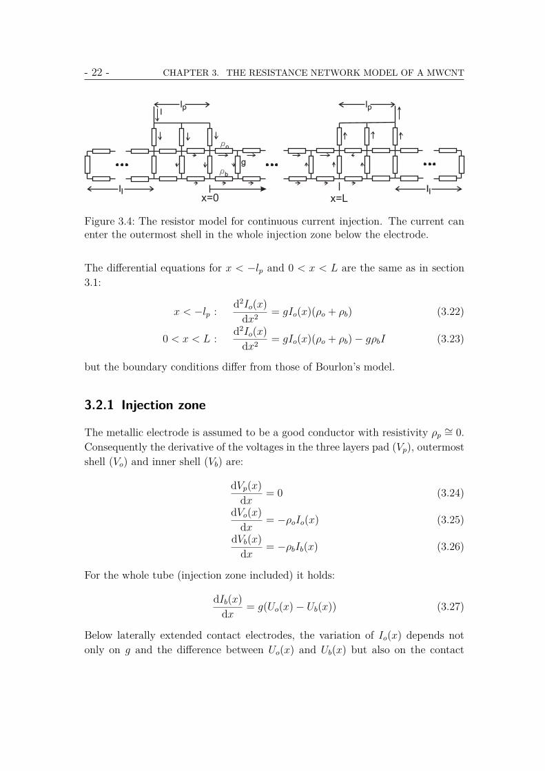
- 22 - CHAPTER 3. THE RESISTANCE NETWORK MODEL OF A MWCNT
ro
rb
g
I
x=0 x=Lll
lp
ll
lp
Figure 3.4: The resistor model for continuous current injection. The current canenter the outermost shell in the whole injection zone below the electrode.
The differential equations for x < −lp and 0 < x < L are the same as in section3.1:
x < −lp : d2Io(x)dx2 = gIo(x)(ρo + ρb) (3.22)
0 < x < L : d2Io(x)dx2 = gIo(x)(ρo + ρb)− gρbI (3.23)
but the boundary conditions differ from those of Bourlon’s model.
3.2.1 Injection zone
The metallic electrode is assumed to be a good conductor with resistivity ρp ∼= 0.Consequently the derivative of the voltages in the three layers pad (Vp), outermostshell (Vo) and inner shell (Vb) are:
dVp(x)dx = 0 (3.24)
dVo(x)dx = −ρoIo(x) (3.25)
dVb(x)dx = −ρbIb(x) (3.26)
For the whole tube (injection zone included) it holds:
dIb(x)dx = g(Uo(x)− Ub(x)) (3.27)
Below laterally extended contact electrodes, the variation of Io(x) depends notonly on g and the difference between Uo(x) and Ub(x) but also on the contact

CHAPTER 3. THE RESISTANCE NETWORK MODEL OF A MWCNT - 23 -
conductivity σ and the difference between Uo(x) and the constant Up(x) = Up :
dIo(x)dx = g(Ub(x)− Uo(x)) + σ(Up − Uo(x)) (3.28)
Once again, differentiating equation 3.28 and inserting 3.24 - 3.26 results in:
d2Io(x)dx2 = g(ρoIo(x)− ρbIb(x)) + σρoIo(x) (3.29)
Since the electrode is a conductor with ρp ∼= 0 the injection point in the electrodeis not relevant. Nevertheless for this model it is useful to consider the connectionpoints to be the leftmost (rightmost) point of the left (right) electrode. In thiscase, the total current for all three layers is I, i.e. Ib(x) = I − Ip(x) − Io(x).Inserting in equation 3.29 results in:
d2Io(x)dx2 = g(ρoIo(x)− ρu(I − Io(x)− Ip(x))) + σρoIo(x) (3.30)
The current leaving the electrode is equal to the injected current in the outermostshell:
dIp(x)dx = σ(Uo(x)− Up)) (3.31)
Differentiating this equation and inserting equations 3.24 and 3.25 results in thelast required differential equation:
d2Ip(x)dx2 = −σρoIo(x) (3.32)
3.2.2 Boundary conditions
Although all described differential equations are analytically solvable and theboundary conditions can be fixed accordingly, it was not possible to generate a so-lution for asymmetrically contacted tubes due to limitations of computer power1.For symmetrically contacted tubes the boundary condition for the end of the tubeis:
Io(−ll − lp) = 0 (3.33)
with the length of the protruding part of the tube on one side ll and the widthof the electrode lp. Since everywhere only an infinitesimal amount of current is1The solution for symmetrically contacted tubes will not be displayed explicitly because it fillsseveral tenths of pages.

- 24 - CHAPTER 3. THE RESISTANCE NETWORK MODEL OF A MWCNT
injected, Io(x) has to be continuous:
Io(−l−p ) = Io(−l+p ) (3.34)Io(0−) = Io(0+) (3.35)
and for symmetry reasons:Io(0) = Io(L) (3.36)
The current in the electrode starts at x = −lp with I and decreases to 0
Ip(−lp) = I (3.37)Ip(0) = 0 (3.38)
The last two required boundary conditions result from the differentiability of Ib(x)(see eq. 3.27):
x < −lp: Io(x) = −Ib(x) ⇒ dIb(x)dx = −dIo(x)
dx (3.39)
−lp < x < 0: I = Ip(x) + Io(x) + Ib(x) ⇒ dIb(x)dx = −dIo(x)
dx − dIp(x)dx (3.40)
=⇒ I ′o(−l−p ) = I ′o(−l+p ) + I ′p(−l+p ) (3.41)
Similarly for x = 0:I ′o(0−) + I ′p(0−) = I ′o(0+) (3.42)
The system of differential equations given by 3.22, 3.23, 3.30 and 3.32 togetherwith the boundary conditions 3.33 - 3.38 and 3.41 - 3.42 was solved using Maple.
Unlike in the model with punctual current injection, the contact resistance withthe voltage step between Up(0−) and Uo(0+) is not obvious, but has to be calculatedfrom equation 3.31. If the electrode is set to ground potential Up = 0, the voltageat the tube resulting from the contact resistance at x = 0− is:
Uo(0−) = 1σ
(I ′p(0−) + Up
)=I ′p(0−)σ
(3.43)
Consequently the voltage for the outermost shell of the tube is:
Uo(x) =I ′p(0−)σ− ρo
x∫0
Io(t)dt (3.44)

CHAPTER 3. THE RESISTANCE NETWORK MODEL OF A MWCNT - 25 -
Figure 3.5: Current in the outermost and the inner shell calculated with con-tinuous current injection for varying lengths. I = 1 µA, ρo = ρb = 10 kΩ/L,g = 10−1 k−1Ω/L, σ = 0.002 Ω−1/L and lp = 0.2L.
And similarly:
Ub(x) = −I′b(0−)g
+I ′p(0−)σ− ρb
x∫0
Ib(t)dt (3.45)
3.2.3 Discussion
Since the differential equations for the region between and the region beyondthe electrodes are the same as in the model with punctual current injection thesolutions appear similar. Especially in the region between the electrodes, thenumerical values of the constants differ only slightly.
Due to the finite length of the tube, in the region beyond the electrodes no constantcan be set to zero. This is a result of the current decay having to be completeat x = −ll − lp. A result is that the nonlocal current as well as the maximumcurrent in the inner shell depend strongly on ll (see fig. 3.5). Because the localpotential is proportional to the integral of the current Io(x), both the gradient andthe bending of the potential profile between the electrodes depend on the totallength (see fig. 3.7). Furthermore, the bending depends mainly on the ratio of ρuto ρo and on g. For small intershell conductance evidently only a small amountof current can enter the inner shell. It is equally clear that the current prefers toflow in the inner shell if ρb < ρo.

- 26 - CHAPTER 3. THE RESISTANCE NETWORK MODEL OF A MWCNT
Figure 3.6: The current distri-bution in the injection regionstrongly depends on σ. For smallσ the current decays linearly inthe outer shell, while for largerσ or larger electrodes injectionoccurs mostly at the edge ofthe electrodes. The current inthe inner shell is only slightlydependent on σ. Except σ, theparameters are the same as in fig.3.5.
The current in the injection region depends strongly on the contact conductivityσ. For a small conductance the current density is nearly homogeneous in the wholeinjection region leading to a linear increase of current in the outermost shell. Ahigher value for σ leads to an injection mainly at the ends of the electrodes andconsequently reduces the current below the center (fig. 3.6). Large electrodesamplify this effect. Therefore the contradiction between the results of Wakayaet al. [95] that the contact resistance depends on the contact length and that ofMann et al. [96] that the current injection mainly occurs on the electrode edges,can be traced back to differences in the contact conductivity. This is plausiblesince Mann et al. used mainly Pd contacts known to have considerably lowercontact resistivity than the Ti/Au contacts used by Wakaya et al..
Since the current density between the electrode and the outermost shell dIp(x)dx =
σUo(x) are small in the center of the contact, the voltage is also small. Neverthelessthe contact resistance defined by the voltage Io at x = 0 is finite because of thefinite integral over the region where the current is actually injected.
Fig. 3.7 shows the potential profile for the outermost shell for different tubelengths. The local potential between the electrodes remains nearly constant forll ≥ L but changes noticeably for shorter tubes. This is a result of smaller currentin the inner shell of shorter tubes (fig. 3.5). The nonlocal potential depends alsoon the tube length since the current for x < −lp is smaller for shorter tubes. Thecurrent decreases to zero at the end of the tube, consequently the tangent of Vo(x)at this position has to be parallel to the x-axis.

CHAPTER 3. THE RESISTANCE NETWORK MODEL OF A MWCNT - 27 -
Figure 3.7: Potential profiles for three different tube lengths. Especially for smallll the gradient of the local potential changes drastically. The tangent at x = −ll−lpis parallel to the x-axis. Same parameters as in fig. 3.5.
3.3 Comparison of both models
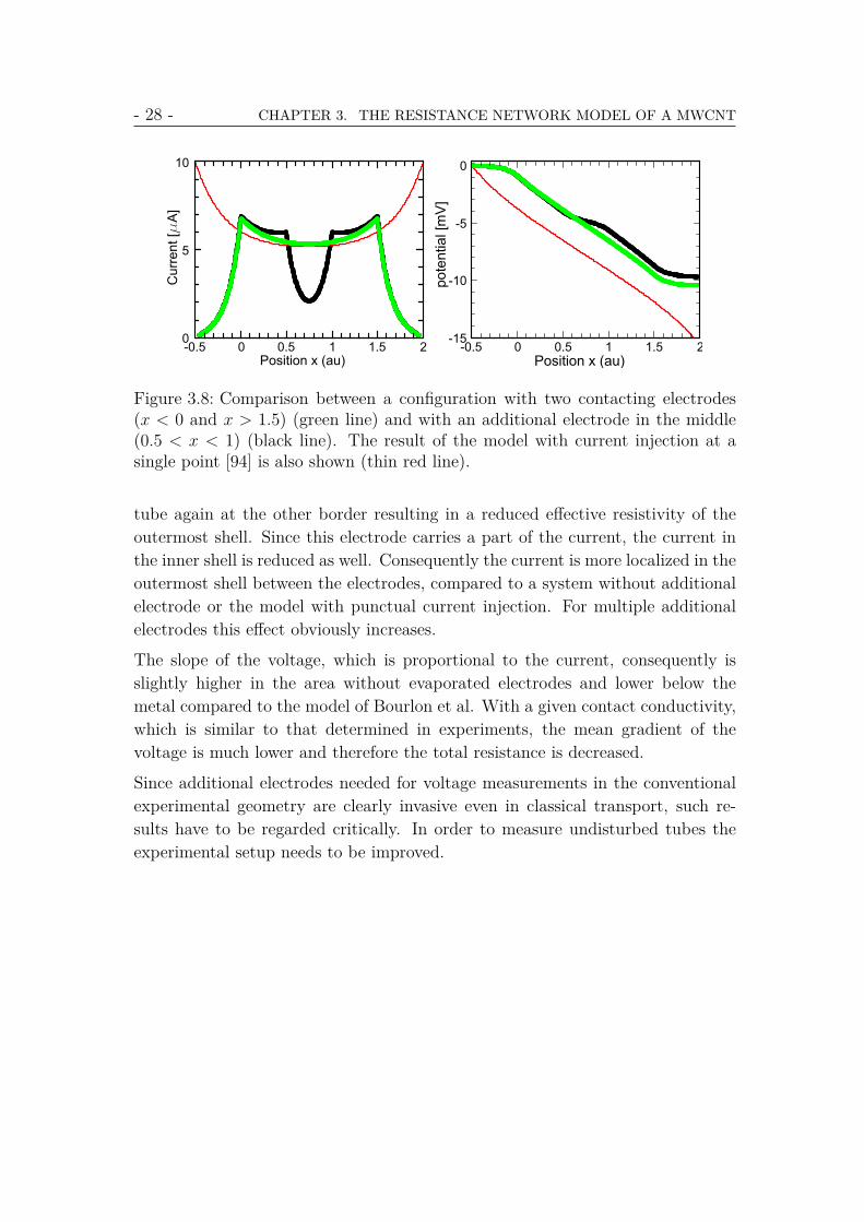
In their experiment Bourlon et al. [94] evaporated 200 nm broad metal electrodesseparated by 200 nm free tube area, using two of them for current injection and twofor voltage measurements. To compare his setup to one with solely two evaporatedinjection electrodes a model with an additional centered electrode in between wascalculated. The differential equations for the third electrode are the same as thatof the injecting electrodes. The boundary conditions for Io(x) are determined inthe same manner as in section 3.2.2 for the outer pads. Since no total currentflows through the center electrode the condition Ip(x) = 0 holds for both ends ofit.
The results for current and voltage1 are shown in fig. 3.8, calculated with con-tinuous current injection (thick black line) and with punctual current injection2
(thin red line). For reference, the potential profile without additional electrode isalso shown (green line). The same parameters were used for all calculations. Thecurrent in the outer shell is obviously strongly reduced below the metal electrodes.The current exits the tube at the beginning of the middle contact and reenters the
1Since the model with punctual current injection has no intrinsic contact resistance, the contactresistance was also not calculated for the new model.
2For the model with punctual current injection a center electrode does not change anything.
- 28 - CHAPTER 3. THE RESISTANCE NETWORK MODEL OF A MWCNT
Figure 3.8: Comparison between a configuration with two contacting electrodes(x < 0 and x > 1.5) (green line) and with an additional electrode in the middle(0.5 < x < 1) (black line). The result of the model with current injection at asingle point [94] is also shown (thin red line).
tube again at the other border resulting in a reduced effective resistivity of theoutermost shell. Since this electrode carries a part of the current, the current inthe inner shell is reduced as well. Consequently the current is more localized in theoutermost shell between the electrodes, compared to a system without additionalelectrode or the model with punctual current injection. For multiple additionalelectrodes this effect obviously increases.
The slope of the voltage, which is proportional to the current, consequently isslightly higher in the area without evaporated electrodes and lower below themetal compared to the model of Bourlon et al. With a given contact conductivity,which is similar to that determined in experiments, the mean gradient of thevoltage is much lower and therefore the total resistance is decreased.
Since additional electrodes needed for voltage measurements in the conventionalexperimental geometry are clearly invasive even in classical transport, such re-sults have to be regarded critically. In order to measure undisturbed tubes theexperimental setup needs to be improved.

4 Experimental Setup
The last chapter described the influence of invasivie contact electrodes which dis-turb the conducting properties of a carbon nanotube even if transport occursclassically. In the quantum conductance limit (i.e. mostly at low temperatures)it was already reported that evaporated electrodes can disturb the wave functiondrastically up to dividing the tube in several quantum dots [71]. Therefore muchless invasive voltage probes have to be used.
An interesting approach uses evaporated electrodes for current injection andMWCNTs as voltage probes. Since nanotubes are cylindrical, the contact ar-eas are small and the probes have high contact resistance as shown in [72], andtherefore are noninvasive for quantum transport, too. Furthermore, the positionof the CNT probes could be adjusted by means of shifting them with an AFM[72]. Since relatively thick MWCNTs were used, the error in the lateral positionis rather large.
Another approach measuring the potential profile along a nanotube is using anEFM. In this method an AFM with a conducting tip measures at a small fixedheight above the sample the local electrostatic force between the sample and thetip that is set to a constant potential [60]. Since also neighboring parts of thetube contribute to the force, the lateral resolution is limited by the distance ofthe tip to the sample and the radius of the tip. In ref. [60] the lateral resolutionis about 100 nm.
An early experiment using movable nanocontacts was performed by Dai et al.[97]. The authors produced Au patterns using conventional lithography methodsthat covered parts of carbon nanotubes by accident. Using them as first electrodeand the tip of a conducting AFM as second one, they measured the two pointresistance versus length. Since the contact quality between tip and nanotube variesfor different positions and due to the typical problem in two point measurementsthat it is not possible to distinguish between intrinsic and contact resistance, theuncertainty in the resistance is relatively high.
Trying to combine the accuracy of a four point measurement with the good lateral
29

- 30 - CHAPTER 4. EXPERIMENTAL SETUP
resolution of a conducting AFM leads to the experiment of Yaish et al [62]. Theycontacted a nanotube with two patterned gold electrodes used to drive a currentand an additional direct contact in between the electrodes using the tip of aconducting AFM which acted as a voltage probe. With the tip moving along thetube the potential versus position can be measured. A disadvantage of this methodis that the contact mode of the AFM, damages the tube by and by. Furthermore,the force pressing the tip onto the tube can induce deformations and the directcontact between tip and tube can generate Schottky barriers [62].
Here we present a new STM based technique with a higher lateral resolutionthan with AFM and a good accuracy in voltage measurements which works in anoncontact technique.
4.1 Sample design
The following approach to measure the potential profile of a carbon nanotube witha STM needs a dedicated sample design. Since the feedback loop regulates theheight of the tip using the tunneling current to the sample, it cannot operate oninsulating substrates. On the other hand, for electron transport measurementsthe substrate has to be insulating because otherwise the transport properties ofthe sample cannot be separated from that of the substrate.
At first view these two requirements seem to contradict each other. To solve thisdiscrepancy, a stack of a metallic layer followed by a thin insulating layer wasproduced on the sample substrate. For the conducting layer tantalum was chosenbecause it grows with a smooth surface on highly doped silicon with thermaloxide on top. The metal was deposited via standard magnetron sputtering. Theinsulating layer, however, was built in a two step process. First, a thin aluminumlayer of 8 A but completely covering the fresh Ta layer below was sputtered in thesame chamber. Then the aluminum layer was oxidized for 15 minutes in 300 mbarpure oxygen, now forming the insulating Al2O3 layer. The implementation ofoxygen results in an increased thickness of the layer of about 1.2 nm.
To investigate the quality of the tunneling barrier, a square Au pattern with30 µm side length was evaporated. Contacting both, the pattern above and theTa layer below, the I-V characteristics of the Al2O3 barrier were recorded. Atypical example for a good barrier is shown in fig. 4.1. Good barriers enduredvoltages up to 2.5 V until they were destroyed. Referring to Brinkman and Dynes[98], the tunneling characteristic can be described with a polynomial of degree

CHAPTER 4. EXPERIMENTAL SETUP - 31 -
Figure 4.1: I-V characteristics of agood Al2O3 barrier. The red curveis the fit with the formalism ofBrinkman [98]. Since the bias volt-age on a nanotube sample is of theorder of 20 µV and the evaporatedarea of the electrodes is below thissquare, the leakage current is lowerthan 10 pA.
three. The parameters of the tunneling process can be determined easily from itscoefficients (the procedure is described in detail in ref. [99]). Based on the fit infig. 4.1 the tunneling parameters were determined:
average barrier height ϕ = 0.63 eVtunneling distance d = 2.3 nm
The tunnel barrier height ϕ is lower than expected for Al2O3. In contrast, thevalue of the tunneling distance d is larger than the expected 1.2 nm. The reducedeffective barrier height and the increased distance is an effect of inhomogeneitiesin the thickness of the insulating layer.
To generate a coordinate system on the sample, alignment marks were evaporatedusing lithography and lift-off techniques. The Ta/Al2O3 bilayer was patternedsubsequently in squares with a side length of 200 µm using lithography and dryetching methods. This allows evaporating contact fingers that reach out of thearea with the thin and sensitive insulating Al2O3 layer to the more stable 300 nmthick SiO2 covered Si substrate. Since these contact fingers cross the edge of thesquare with the exposed Ta layer in the cross-section, an additional insulatingmaterial was grown around the squares. This was SiO2 in the case of samples Band D via PECVD1 and Al2O3 in the case of samples A and C via ALD2.
Multiwall carbon nanotubes were suspended on the surface from a solution inorthodichlorbenzene by applying a drop of the solution on the sample and flushingit after some time with isopropanol. The nanotubes that hit the substrate stickon it due to Van der Waals forces. The positions of the tubes relative to thealignment marks were determined in a scanning electron microscope (SEM). Since
1Plasma-enhanced chemical vapor deposition2Atomic layer deposition

- 32 - CHAPTER 4. EXPERIMENTAL SETUP
Figure 4.2: On the Si substrate with 300 nm thermal oxide, a stack of Ta and a thinAl2O3 layer was prestructured. The nanotube is contacted with Pd/Au electrodesreaching down from the prestructured square to the SiO2 covered substrate. Unlikein the drawing, the sides of the Ta film are also covered with an insulating material.
the alignment marks are visible under the PMMA1 electron lithography resist,the contact electrodes can be defined directly on the tube using electron beamlithography. Furthermore, conductive paths out of the prestructured squares havebeen defined. After evaporating the metal electrodes and a subsequent lift-off stepthe sample is ready for use. A schematic drawing is shown in fig. 4.2.
Several experimental works revealed that transport properties of Pd contacts aresuperior to other metals. The contact resistance is lower [96, 100, 101] and theformation of Schottky barriers is strongly reduced [102]. Ab initio calculationsof Nemec, Tomanek and Cuniberti [103] confirm these results tracing back thesuperiority of Pd to metal-nanotube hybridizations.
To benefit from the good contact properties the metal electrodes consist of athin (≈ 3 nm) layer of Pd, followed by a thicker Au layer in order to reduce thetotal resistance in the electrode. Additional bigger Cr/Au squares adjacent to thecontact lines on the SiO2 allow connecting supply lines.
4.2 Measurement setup
The complete sample preparation takes place under clean room conditions. Themeasurements, however, have been performed under clean ultra high vacuum con-ditions in the UHV-Nanoprobe consisting of four independent scanning tunnelingmicroscopes (STM) (see fig. 4.3). Furthermore, a scanning electron microscope(SEM) is mounted in the vacuum chamber, required for positioning the tips on thesample. Additional features of the system are an electron spectrometer for scan-1Poly(methyl methacrylate)

CHAPTER 4. EXPERIMENTAL SETUP - 33 -
Figure 4.3: The UHV-Nanoprobe (Omicron) consisting of the sample stage in thecenter and the four stages for the tips. The tips are attached at the end of thecantilevers above the sample stage. All five stages are movable in x and y directionand the tip stages additionally in z direction. The tip cantilevers are magneticallyheld on 90 quadrant piezo tubes. The oxygen free Au-coated copper braid usedfor cooling is visible on the right side of the image.
ning Auger measurements and a Mott detector for scanning electron microscopywith (spin) polarization analysis (SEMPA). The attached preparation chamberwas used in this work for tip preparation, but can also be used for sample clean-ing via heating and sputtering and evaporating thin metal layers epitaxially.
Attention should be paid to the fact that the two imaging methods SEM and STMaffect each other. The metallic tips disturb the distribution of the electric fieldabove the sample and therefore deform the electron beam of the SEM affectingits resolution. The SEM on its side deposits electrons on a STM tip or at leastsecondary electrons caused by the electron beam hit the tip contributing to thetotal current detected by the feedback control. Since only low tunnel currentshave been used in this work (see below) this current exceeds the setpoint causingsetpoint detection on every height or, with the other sign, tip crashing.
For the measurements reported in this work two Au tips, attached on geometricallyadequate cantilevers, have been used to contact the square contact pads on theSiO2 and in order to drive the current through the nanotube with a constantcurrent source1. A third tip, made of tungsten for better stiffness, was used topierce the Al2O3 layer and contact the Ta layer below the nanotube. It can beused to ground the conducting layer in order to allow tunneling current to theSTM tip for imaging or to apply a gate voltage in the potentiometric mode.
1Keithley 6221

- 34 - CHAPTER 4. EXPERIMENTAL SETUP
10 mm
Figure 4.4: Left: A schematic drawing of the measurement setup. A current Isis driven through the nanotube via evaporated electrodes. The tunneling voltageUT is applied between the tip and one electrode and the tunneling current IT ismeasured. Right: SEM image of the sample with the tip piercing the oxide layer(on the left) and the tip used for probing the potential at the tube that is betweenthe thin electrodes.
At the forth tip position a sharp W tip1 was applied and used for imaging thetube and for the potentiometric measurements. The measurement setup is shownschematically in fig. 4.4.With both, the Ta layer and at least one electrode on ground potential, the STMtip was used to locate and image the tube. Since the effective tunnel barrier is thesum of the insulating Al2O3 layer and the gap between the tip and the surface,the feedback parameters have been chosen carefully to avoid a crash with thesurface. In the experiment a tunnel voltage of UT = 2 V and a current setpointof IT = 20 pA were found to be reasonable. The strong increase in the tunnelcurrent at this voltage might be an effect of image potential states at this energy[104].After locating the tube and final positioning of the scanning area, the potentio-metric measurement has been started. For this purpose the current in the tubewas switched on and the tip was positioned on the tube. Switching off the feed-back loop and lowering the tunnel distance a few angstrom results in a bettercontact between tip and tube but remains noninvasive since the tunnel characterpersists. After taking an I-V characteristic, the feedback loop was turned on againand a new position has been approached. At the zero crossing of the I-V -curve1All used W tips were heated in UHV conditions to at least 1000 C to remove oxide. After thisa small tip radius was confirmed with field emission current between the tip and a surface at adistance of ≈ 1 mm.

CHAPTER 4. EXPERIMENTAL SETUP - 35 -
the current flow is disabled because the potential difference between tip and theposition on the tube below is zero. The voltage on this balanced point is easy toread out and represents the potential of the outermost shell of the tube. Plottingagainst the position on the tube yields the potential profile. The lowering of thetunnel distance does not affect the measured potential [105], but improves themeasurement accuracy.
This is strictly valid only in the case of diffusive transport where the electronsare nearly in an equilibrium state for every position of the tube. In this case theFermi distribution is valid and defines the electrochemical potential. For pureballistic transport, however, one expects two different electrochemical potentialsfor electrons with k-vectors pointing from left to right and vice versa. This resultsbecause the two electron reservoirs of the electrodes can only inject electrons withk-vectors pointing away from the electrode and up to their Fermi level. Assum-ing highly transparent contacts and neglecting backscattering at the nanotube-electrode interfaces results in two different electrochemical potentials for the twodirections of the k-vectors according to the potentials in the electrodes.
If impurities in the tube and backscattering effects at the tube-metal interfacesare considered, the picture becomes more complicated. A sufficient descriptioncan be achieved with the Buttiker formula [106–108]. The present setup can bedescribed as a three terminal geometry with two contact electrodes (terminals 1and 2) and the STM tip (terminal p). The total current Ip in the tip which isused as a probe is the sum of the currents originating from contacts 1 and 2.The current between two terminals α and β can be written as a product of thetransmission probabilities Tαβ and the differences of the electrochemical potentialsµα and µβ of the contacts, respectively. Therefore the total current in the probeis:
Ip = 2eh
(Tp1(µp − µ1) + Tp2(µp − µ2)) (4.1)
In principle, a current flow in the probe is not necessary for voltage measurements.This can be fulfilled if the probe is floating or with a voltage compensation. ForIp = 0 equation (4.1) can be solved:
µp = T31µ1 + T32µ2
T31 + T32(4.2)
If the probe is weakly coupled to the conductor at a single point (tunneling bar-rier), scattering with the lead is suppressed and the potential in the probe isindependent of the strength of the coupling to the conductor and of the density

- 36 - CHAPTER 4. EXPERIMENTAL SETUP
of states in the probe [105]:
µp = νx1µ1 + νx2µ2
ν(x) (4.3)
with νxα being the injectivities of contact α to the tube point x with the localdensity of states ν(x). Since all terms in equation (4.3) are independent of thepresence and properties of a probe, it does not disturb the intrinsic transportproperties and can be used to define an electrochemical potential for each position.It should be remarked that the Fermi distribution is only valid in the probe itself,whereas the electrons inside the conductor are in a nonequilibrium state.
The contact between the STM tip and the MWCNT has typically spatial di-mensions of the order of one or a few atoms and due to the STM equipment thecontact can be held in tunneling state. Therefore this contact is weak in the mean-ing mentioned above. Unlike to commonly used voltmeters with finite impedance,the employment of the tunneling I-V characteristics leads to no current at allthrough the probe at the zero crossing. Thus the applied voltage is equal to thepotential of the probe in floating state.
In the classical limit (many scattering events which destroy phase coherence)the transmission probabilities depend mainly on the number of scattering events.Since the phase destroying electron-phonon end electron-electron scattering is notlocalized but equally distributed in the conductor, the distance between the probeand the contact dominates the transmission probability. In an adiabatic limitwhere enough scattering events occur so that the electrons are in an equilibriumstate at every position, the Fermi distribution is valid in the conductor and themeasured electrochemical potential is the Fermi level.
5 Results obtained at roomtemperature
As discussed in the last chapter in principle STM based potentiometry is a non-contact method and therefore the tube is not damaged during the measurements.Since the feedback parameters have to be adjusted adequately to not crash thetip on the oxide overlayer, the tunnel conditions at the metal electrodes are notideal. In fact the tunnel contact is so instable that several spikes in the currentimage appear indicating direct contact between tip and electrodes. Since the tipis charged to a voltage of 2 V this produces voltage peaks close to the breakdownvoltage of the thin insulating spacer to the bottom electrode.
After all, the advantage over the AFM method, of not damaging the tube is coun-terbalanced by the disadvantage of destroying the oxide layer below an electrode.As soon as one electrode has contact to the Ta layer, voltage peaks can be di-verted by this conducting channel including the nanotube, protecting the secondelectrode. So, only samples with a high quality insulator withstand the imagingprocedure without contact to the metallic sublayer. In this work only one sample’sinsulating barrier rested completely intact during the measurement of the poten-tial profile: Sample C (section 5.3). In this case the Ta layer can be additionallyused as a back-gate.
In all other samples one of the injection electrodes has ohmic contact to themetallic layer. Therefore it is set to ground potential and the intact electrode isused to apply an adequate voltage. If no other value is mentioned the currentthrough the tube was set to IT = 1 µA.
37

- 38 - CHAPTER 5. RESULTS OBTAINED AT ROOM TEMPERATURE
Figure 5.1: SEM images of the multiwall carbon nanotube without obvious defects(sample A). Left: The tube on the surface without electrodes. The distance ofthe alignment marks is 10 µm. Right: the same tube with evaporated Pd/Auelectrodes.
5.1 Sample A: a multiwall carbon nanotube with noobvious defects
A MWCNT with no obvious defect was selected and contacted with metal elec-trodes (fig. 5.1) as described in chapter 4. The SEM image (fig. 5.1) reveals adiameter of d ≈ 33 nm. The metal electrodes were evaporated asymmetrically inorder to leave a sufficiently long part of the tube beyond the contacts to allowlocal as well as nonlocal measurements.In the STM images (fig. 5.2) the electrodes and the nanotube itself appear to beexpanded compared to the SEM images in fig. 5.1. This broadening is due to thegeometry of the tip relative to the sample. Since the tip and the sample surfacedraw an angle of about 50-60 every structure with nonzero height results in alateral enlargement in the STM image raked at one edge. Furthermore, due tothe not perpendicular tip direction a sideways part of the tip scans the surface,where the radius of curvature exceeds that of the tip.Additionally, since the tunnel parameters are optimized for scanning over theoxide layer, the feedback parameters are not ideal for the highly conductive metalinjection electrodes and the CNT. As described above there are even short-circuitspikes in the current, causing the feedback loop to overshoot in retracting thetip. The following decrease of the sample tip distance is limited to the differencebetween the actual current and the set-point. This difference can be at maximumequal to the set-point which is set to a few pA. Consequently spikes appear in the

CHAPTER 5. RESULTS OBTAINED AT ROOM TEMPERATURE - 39 -
Figure 5.2: STM images of sample A between the electrodes (left) and beyond theelectrodes (right).
line-scans of the topography with a high gradient at one side and a milder slopewhen lowering the tip again. This effect also increases the width of conductingpatterns in the STM image.
Due to limitations in the scan-range the local and non-local potential measure-ments were done at different stage positions. To connect both potential profiles inthe local as well as in the non-local measurement series, points at both sides of theelectrode were measured. The combined potential profile is shown in fig. 5.3 (blackfilled circles) for a constant current of 1 µA. The curvature of the local potentialis noticeable as well as the exponential like behavior of the non-local potential,both predicted by the resistivity model. For x < 0 nm and 650 nm < x < 830 nmno potential variation could be observed because there the measurements wereperformed on the high conductive contact electrodes.
Conventional fit algorithms do not work with the huge analytic solution of theresistivity model with continuous current injection, at least with the availablecomputer power. So another routine to fit the curves was developed. In this worka procedure similar to the simulated annealing algorithm was chosen. Startingwith reasonable initial values, the parameters were varied by hand and the de-viation was documented. With an understanding which parameter acts on thegradient and the bending at the different parts of the tube an adequate fit canbe obtained much faster than in the purely randomly acting simulated anneal-ing algorithm. However, in both procedures no error for the parameters can becalculated directly. It was estimated by generating fit curves with slightly higherdeviations and monitoring the variation in the parameters.
With this procedure the fit in fig. 5.3 (red line) was built. The resulting parameters

- 40 - CHAPTER 5. RESULTS OBTAINED AT ROOM TEMPERATURE
Figure 5.3: Potential profile of sample A (black filled circles). The simulation ofthe voltage in the outermost shell (red line) fits the measurement well, especiallyaround the second electrode. For the left part a simulation with a smaller contactpad and a tube not exceeding the pads was performed (blue line). In the insetthe current distribution of the two simulated shells in the tube is shown.
are:
resistivity of outer shell: ρo = 52 kΩ/µm± 5 kΩ/µmresistivity of second shell: ρb = 9 kΩ/µm± 3 kΩ/µmintershell conductivity: g = (215 Ω)−1 1/µm± 7× 10⁻⁴ Ω−1/µmcontact conductivity: σ = (147 Ω)−1 1/µm± 2× 10⁻⁵ Ω−1/µm
The error of ρb of 30% is relatively large because this value is extracted mainlyfrom the bending of the curve between the electrodes, whereas the approach for ρois more direct since the potential profile of the outermost shell was measured. Thecurrent that exits the part of the tube between the electrodes depends strongly ong and can be extracted mainly from the potential step between the electrode andthe non-local potential. The contact conductivity σ, however, shifts the potentialjumps at both sides of the electrode.
The simulated curve fits the measurement well, especially for x > 200 nm. The

CHAPTER 5. RESULTS OBTAINED AT ROOM TEMPERATURE - 41 -
Figure 5.4: Simulations of symmetrically contacted tubes with length equal to thedistance between the electrodes (black curve) and a longer tube (red curve). Allother parameters are identical. The reference point for the potential is in themiddle between the contacts. The potential profile of the short tube exhibits astronger bending around the electrodes and also a higher average slope than thelong tube. The insets show the geometrical configurations of the two simulationsfor the black and the red curve, respectively.
deviation for x < 200 nm is easily explained by the asymmetry of the contactelectrodes as shown in fig. 5.1. The fit in fig. 5.3, however, is calculated witha model of a symmetrically contacted tube protruding from both electrodes by420 nm. Fig. 5.4 shows simulations of CNTs exceeding and not exceeding theregion between the electrodes. This single difference in the model parameterscauses a significant variation in the potential profile. Especially in the region nearthe electrodes the tube not exceeding the contacts exhibits a stronger bendingand a significantly higher slope in the potential profile.
If one compares the fit curve with the experimental data it is clear that the fitdeviates mainly around the left electrode where the tube ends below the contact.This is not astonishing because this region is not well reproduced in the symmet-rical model. In this area identical modifications in the profile appear as alreadyshown by the comparison of models of a short and a long tube. The bending is

- 42 - CHAPTER 5. RESULTS OBTAINED AT ROOM TEMPERATURE
stronger around this position and the slope is steeper, as well. Since simulating islimited to a symmetrical model, for the left part of the tube only a model withoutprotrusion and for the right part with protrusion applies. For the middle betweenboth contacts, both models are appropriate. For illustration, in fig. 5.3 for the leftpart a simulation for a tube ending below the contacts was performed (blue line).Apart from the tube length, the same parameters were used.
Considering both, the good fit for x > 200 nm and the good reproduction of themeasured potential for x < 200 nm with the model of a tube not exceeding theelectrodes, it can be concluded that the resistivity model fits well to the situationin the tube.
In the resistivity model only the outermost and one inner shell is considered.Bourlon et al. [94] argued that only a small amount of current enters the secondshell, and therefore even lower currents entering the inner shells can be neglected.They extracted an intershell conductivity leading to a current in the second shellof about 10% of the current in the outermost shell and correspondingly ≈1% inthe third shell.
The simulation of the current flow in this tube, however, shows an amount ofcurrent up to 85% that leaves the outermost shell (inset of fig. 5.3). Assumingthat the intershell conductivity between the second and third shell is in the samerange as between outermost and second, the current in the third shell cannot beneglected any more and consequently the fit parameter ρb cannot be interpreteddirectly as the resistivity in the second shell.
The example of this tube shows that even for shells with an extreme differencein intrashell resistivities the resulting potential profile between the electrodes isroughly linear i.e. tolerates approximation with uniform resistivity. This is shownin fig. 5.5 which compares the potential profiles of the outermost and the innershell in the model using the parameters of this tube. Since current injection in thesecond shell is mainly below the electrodes and near the electrodes the behaviorof its potential profile is similar to that of the outermost shell.
Including additional shells in the model changes the potential profile of the secondshell only slightly since it becomes the “outermost shell of the inner tube”. Con-sequently, the two shell model can also be used to describe tubes with multiplewalls but ρb cannot be directly interpreted as the resistivity of the second shell,but rather as an effective resistivity of the complete inner tube of the second shelland the shells below.
Additionally the remarkably high difference between ρo and ρb far beyond the

CHAPTER 5. RESULTS OBTAINED AT ROOM TEMPERATURE - 43 -
Figure 5.5: Comparison of the potential decrease in the inner and the outermostshell. Between the electrodes (on the left of the vertical line) the potential profileof the inner shell is similar to that of the outermost and both are approximatelylinear.
errors attracts attention. Bourlon et al. [94] explain these differences due toadsorbates or defects in the outermost shell, whereas the lower shells are pro-tected by the outermost one. Another interpretation is that the outermost shellhas a semiconducting shell1 and the inner tube can be metallic. Additionally theremarkably high difference between ρo and ρb far beyond the errors attracts atten-tion. Bourlon et al. [94] explain these differences due to adsorbates or defects inthe outermost shell, whereas the lower shells are protected by the outermost one.Another interpretation is that the outermost shell has a semiconducting shell2 andthe inner tube can be metallic.The intershell conductivity in our tube, however, is much higher than that deter-mined by Bourlon et al [94]. The highest intershell conductivity determined withtheir method using an array of evaporated contacts is as low as 3.7−1 kΩ−1/µm.Unfortunately they do not give the exact values for the diameters of their tubesbut only a range in the order of about 10 nm. To exclude the influence of thediameter, the volume resistivities3 have to be compared. The results of Bourlon1A carbon nanotube of a diameter of ≈ 30 nm has a band gap of about 23 meV [109] slightlybelow the thermal energy at room temperature. Consequently, charge carriers can be thermallyexcited.
2A carbon nanotube of a diameter of ≈ 30 nm has a band gap of about 23 meV [109] slightlybelow the thermal energy at room temperature. Consequently, charge carriers can be thermallyexcited.
3As the term “resistivity” is used for resistivity of 1D materials in this work, “volume resistivity”

- 44 - CHAPTER 5. RESULTS OBTAINED AT ROOM TEMPERATURE
et al. [94] show a range of 0.34 Ωm-1.8 Ωm. Compared to the value of this tubeof 0.068 Ωm, there is still a factor 5 left. One reason for this difference are theevaporated voltage probe electrodes which localize the current in the outermostshell as mentioned in section 3.3 and therefore suppress intershell conductance.
Another explanation may arise from the difference of the diameters. For diameterslarger than 15− 20 nm polygonal cross sections have been observed [28, 110]. Inthis range the intershell spacings that are up to 0.39 nm for thin tubes decrease tonearly that of graphite of 0.34 nm for small tubes [111]. Both results indicate thatfor large diameters the tubes consist of several planar regions joined together. Itcan be imagined that in some of this planar regions the stacking is like in graphite.In such parts of the tube it is obvious that also the intershell coupling is comparableto that of graphite.
In the literature the volume resistivity of pure graphite in c-direction i.e. perpen-dicular to the layers spreads from 4.3 10−5 Ωm to 6.7 10−5 Ωm [112, 113], depend-ing strongly on the quality of the crystal. Even highly oriented pyrolytic graphite(HOPG) shows a volume resistivity up to 100 times higher along the c-axis thansingle crystals [113].
The volume resistivity of our tube is between the values found by Bourlon et al.[94] for smaller diameter tubes and that of graphite, indicating at least some areaswith good intershell conductance. Since the value still differs from that of singlecrystals by a factor of 103 an exact graphitic stacking even in small parts can beexcluded. In fact, if planar regions in our tubes exist, the interlayer coupling isstrongly decreased probably due to incommensurate stacking. This reduction inthe interlayer coupling was also observed in twisted graphene [114].
Furthermore, for thicker tubes the 1D sub-bands are moving together giving riseto the presumption that an unavoidable doping causes more channels contributingto electron transport. Our measurements, however, reveal higher values for theintrashell resistivities. Consequently, the difference in diameter alone cannot beresponsible for the discrepancy between the experimental data.
Summarizing we state that our resistivity model fits well the measured potentialprofile for the local as well as for the non-local potential measurements. Devia-tions at one side of the curve can be explained by the asymmetry of the contactelectrodes. The bending of the measured potential profile between the electrodescan only be explained by a much lower resistivity of the inner tube than of the
was chosen to identify the conventional resistivity in a 3D material ρ = EJ with the electric field
E and the current density J .

CHAPTER 5. RESULTS OBTAINED AT ROOM TEMPERATURE - 45 -
outermost shell. Since a large part of the current leaves the outermost shell itcan be assumed that non-negligible parts of the current enter the third shell andeven shells further below. Consequently, ρb has to be interpreted as an effectiveresistivity of the inner shells. Although the tube has a diameter usually yieldinga polygonal cross-section, graphitic stacking can be excluded since the intershellconductivity is too low.
5.2 Sample B: a multiwall carbon nanotube with anincomplete outermost shell
For this sample a multiwall carbon nanotube with an incomplete outermost shellwas contacted with 200 nm broad and 120 nm high Pd/Au injection electrodes.The SEM image (fig. 5.6 (b)) shows a slight change in diameter indicating theposition where has lost the outermost shell of the left side. The mean diameter isabout 30 nm. Fig. 5.6(a) shows an illustration of the two outer shells of the tubeand the transition from a n-shell tube to a (n-1)-shell tube. The inner shells wereleft out for clarity.
The two point resistance between the electrodes was R2P = 14.4 kΩ which isconsistent with the intrinsic resistivities for MWCNTs of≈ 10 kΩ/µm plus contactresistances of ≈ 2 kΩ for highly transparent contact electrodes. The potentialmeasurement was performed for a current of I = 1 µA and for I = −1 µA. Sincethe left electrode had direct contact to the Ta layer it was set to 0 V for bothmeasurements. As expected for diffusive electron transport, each potential profileis the mirrored one of the other (fig. 5.7). Both exhibit a potential jump of≈ 1.5 mV at the position where the outermost tube ends at x = 260 nm. Mergingthe negative of the potential profile with I = −1 µA with that with I = +1 µAresults in a uniform curve (open circles in fig. 5.6(c)). At x = 260 nm the currentmust eventually leave the outermost shell completely and is forced to enter lowershells. This potential step is therefore direct evidence of intershell current flow inthis particular MWCNT.
Since the resistivity model in chapter 3 includes only complete shells it is improperfor the situation in this tube. Furthermore, at least one additional shell has to beintroduced to distinguish the part without the outermost shell from a single walltube. Consequently, a model suitable for this tube has to include three shells atthe left part and two shells at the right part of the tube. Additionally the tubeis no longer symmetric, therefore for a similar model all the parts (left beyond
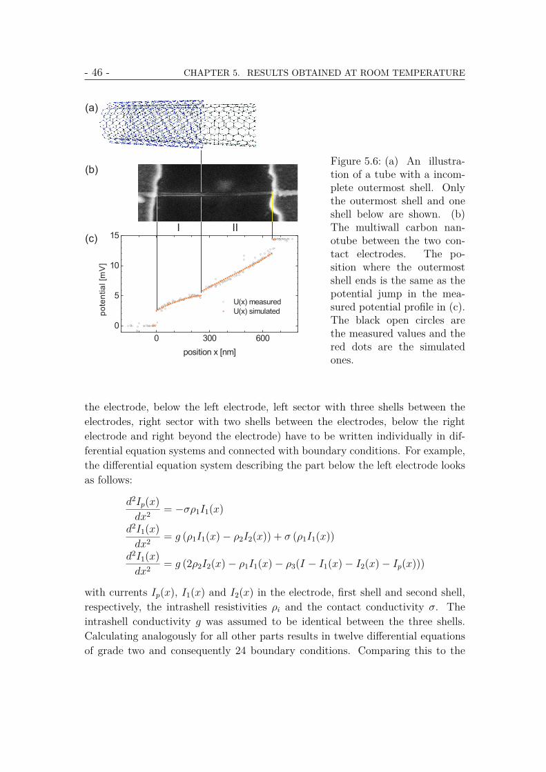
- 46 - CHAPTER 5. RESULTS OBTAINED AT ROOM TEMPERATURE
0 300 600
0
5
10
15
po
ten
tia
l[m
V]
position x [nm]
U(x) measured
U(x) simulated
(b)
(a)
(c)I II
Figure 5.6: (a) An illustra-tion of a tube with a incom-plete outermost shell. Onlythe outermost shell and oneshell below are shown. (b)The multiwall carbon nan-otube between the two con-tact electrodes. The po-sition where the outermostshell ends is the same as thepotential jump in the mea-sured potential profile in (c).The black open circles arethe measured values and thered dots are the simulatedones.
the electrode, below the left electrode, left sector with three shells between theelectrodes, right sector with two shells between the electrodes, below the rightelectrode and right beyond the electrode) have to be written individually in dif-ferential equation systems and connected with boundary conditions. For example,the differential equation system describing the part below the left electrode looksas follows:
d2Ip(x)dx2 = −σρ1I1(x)
d2I1(x)dx2 = g (ρ1I1(x)− ρ2I2(x)) + σ (ρ1I1(x))
d2I1(x)dx2 = g (2ρ2I2(x)− ρ1I1(x)− ρ3(I − I1(x)− I2(x)− Ip(x)))
with currents Ip(x), I1(x) and I2(x) in the electrode, first shell and second shell,respectively, the intrashell resistivities ρi and the contact conductivity σ. Theintrashell conductivity g was assumed to be identical between the three shells.Calculating analogously for all other parts results in twelve differential equationsof grade two and consequently 24 boundary conditions. Comparing this to the
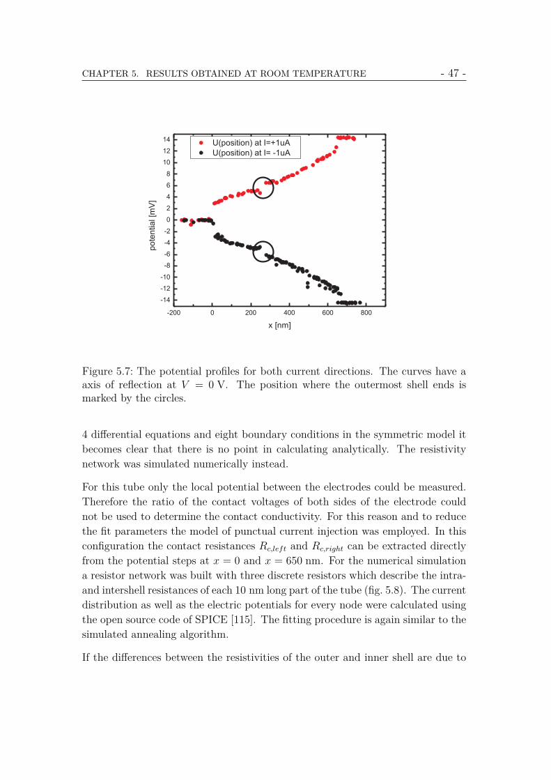
CHAPTER 5. RESULTS OBTAINED AT ROOM TEMPERATURE - 47 -
-200 0 200 400 600 800
-14
-12
-10
-8
-6
-4
-2
0
2
4
6
8
10
12
14
po
ten
tia
l[m
V]
x [nm]
U(position) at I=+1uA
U(position) at I= -1uA
Figure 5.7: The potential profiles for both current directions. The curves have aaxis of reflection at V = 0 V. The position where the outermost shell ends ismarked by the circles.
4 differential equations and eight boundary conditions in the symmetric model itbecomes clear that there is no point in calculating analytically. The resistivitynetwork was simulated numerically instead.
For this tube only the local potential between the electrodes could be measured.Therefore the ratio of the contact voltages of both sides of the electrode couldnot be used to determine the contact conductivity. For this reason and to reducethe fit parameters the model of punctual current injection was employed. In thisconfiguration the contact resistances Rc,left and Rc,right can be extracted directlyfrom the potential steps at x = 0 and x = 650 nm. For the numerical simulationa resistor network was built with three discrete resistors which describe the intra-and intershell resistances of each 10 nm long part of the tube (fig. 5.8). The currentdistribution as well as the electric potentials for every node were calculated usingthe open source code of SPICE [115]. The fitting procedure is again similar to thesimulated annealing algorithm.
If the differences between the resistivities of the outer and inner shell are due to

- 48 - CHAPTER 5. RESULTS OBTAINED AT ROOM TEMPERATURE
Rc,left
Rintershell
Rc,rightRout
Rintershell
Rin
Rin
Figure 5.8: Model with incomplete outermost shell. For numerical simulation thecontinuous model with conductivity g and resitivities ρi was changed to a networkof discrete resistors.
defects and adsorbates in the outermost shell, it can be assumed that only tworesistivities have to be distinguished. One, ρout for the respectively exterior shellthat in our case is the complete outermost shell and the part of the second shellfor x > 260 nm, and ρin for the second shell for x < 260 nm and the completethird shell. On the other hand, if we assume that the resistivities are intrinsicparameters of the three shells, three parameters ρi have to be used for fitting.
We tested both possibilities and the best fit was achieved with ρout = ρin andρ1 = ρ2 = ρ3, respectively. The results are consistent and the simulated curve isshown in fig. 5.6(c) (red dots). The complete set of fit parameters for this tube is:
Rc,left = 2.5 kΩ± 0.2 kΩRc,right = 2.3 kΩ± 0.2 kΩ
g = (100 Ω)−1 1/µm± 2× 10⁻³ Ω−1/µmρ1 = 30 kΩ/µm± 3 kΩ/µmρ2 = 30 kΩ/µm± 3 kΩ/µmρ3 = 30 kΩ/µm− 10 kΩ/µm /+ 30 kΩ/µm
The large error in ρ3 is due to the indirect conclusion from the curvature of thepotential profile mainly for x > 260 nm. The errors of the other parameters areacceptable and the values are in the same range as those of the tube free of obviousdefects. The relative error of g is nearly the same as in the last tube althoughno non-local measurements could be done. The accuracy arises from the strongdependence of g on the potential step at x = 260 nm that could be measured veryaccurately.

CHAPTER 5. RESULTS OBTAINED AT ROOM TEMPERATURE - 49 -
Interestingly, the intrashell resitivities are equal within the experimental error andare between the values of ρo and ρb of the previously described tube. The highresistance of 30 kΩ/µm suggests that all three shells are either semiconductingwith a small band gap or have a high density of scattering centers.
Summarizing the results of this section it can be pointed out that the resistivitymodel provides good fits for the measured potential profile. For this purpose anumerical simulation of a resistor network had to be performed. The deducedfit parameters are consistent with those of sample A. In particular the potentialjump at x = 260 nm was shown to be an effect of the intershell conductivity andcould be measured directly.
5.3 Sample C: A tube with a strongly varyingdiameter
The sample design for sample C is identical with sample A. The unique featureof this sample is a strong change in diameter at x = 270 nm probably due to anintramolecular junction [116]. This sample offers the possibility of back-gated mea-surements since both contact electrodes remained insulated from the Ta layer.Thechange in diameter can be observed in the SEM image (see fig. 5.9). Around theupper contact the diameter is ≈ 29 nm and around the lower one the diameter is≈ 24 nm. In potentiometric measurements x = 0 is at the inner edge of the lowerelectrode. The contact resistance of the second electrode was fluctuating and notstable enough for two point resistance measurements. Nevertheless a reasonablepotential profile in local geometry could be measured since the electrode with thestable contact resistance was used as voltage reference. Measurements in non-localgeometry were only possible beyond this stable contact.
5.3.1 Characteristics without gate voltage
The potential profile (fig. 5.10) exhibits two distinct regions corresponding to thetwo sectors of the tube with different diameters. At the part of the tube thatconnects to the well defined contact local as well as non-local measurements couldbe performed. These measurements can be fitted well with the resistivity model

- 50 - CHAPTER 5. RESULTS OBTAINED AT ROOM TEMPERATURE
Figure 5.9: SEM image of sample C: the radius of this tube exhibits a change indiameter between the electrodes. This part is enlarged to show the transition indetail.
(red line in fig. 5.10). The fit parameters are:
ρo = 47 kΩ/µm± 5 kΩ/µmρb = 40 kΩ/µm± 8 kΩ/µmg = (1033 Ω)−1 1/µm± 2× 10⁻⁴ Ω−1/µmσ = (200 Ω)−1 1/µm± 5× 10⁻⁵ Ω−1/µm
The relative errors, especially for g, are larger than for the samples above. This isdue to the shorter part where the model is appropriate. The intrashell resistivitiesand the contact conductivity are in good agreement with that of samples A andB. The intershell conductivity, however, is smaller than in the samples presentedabove by a factor of 7 - 10. This is manifested in the slight bending of the potentialprofile near the electrode and by the slow decrease in the gradient of the non-localpotential.
Since the intershell conductivity and the difference in the intrashell resistivities ofthis sample are lower than those in sample A the current does not concentrate asmuch in the inner shells (inset of fig. 5.10). Nevertheless in the middle of the tubethe currents in the outermost and the inner shell are in the same range. Thereforefor this set of parameters ρb has to be interpreted as the effective resistivity of thecomplete inner tube, too, meaning that the real resistivity of the second shell islarger than calculated.

CHAPTER 5. RESULTS OBTAINED AT ROOM TEMPERATURE - 51 -
Figure 5.10: Potential profile of sample C. The right electrode with a stable contactresistance was used as voltage reference. The calculated curve (red) fits well themeasurement for x > 270 nm that represents the thicker part of the tube. At thetransition from small to big diameter a potential step occurs followed by a lowerslope for the thinner tube (green line). The unstable contact conductivity at theleft contact causes the potential variation for x < 0. The inset shows the currentdistribution in the outermost and the inner tube within the model.
For the sector connecting to the right contact no non-local potential measurementscould be performed due to the fluctuating contact resistivity. Therefore and due tothe bad signal to noise ratio for x < 270 nm a reasonable fit for the left part of thetube was not possible. For a rough estimate of the main difference we can use themean gradient (green line in fig. 5.10) that is much lower than for the thicker sectorcorresponding to a mean resistivity of 10 kΩ/µm compared to a mean resistivityof 24 kΩ/µm of the right sector. Assuming a similar defect density in the crystallattice in both sectors, we conclude that at least one of the shells must have atransition from a metallic to a semiconducting state. The anomaly at the defectposition can be due to a Schottky barrier. This hypothesis could be tested byreversing the current direction and monitoring potential changes in the potentialprofile at the junction point [116]. As at first we decided to measure the gatedependency of this tube and the sample did not survive that measurement, thereversed current behavior cannot be tested anymore.

- 52 - CHAPTER 5. RESULTS OBTAINED AT ROOM TEMPERATURE
tt
x
7
2x
27
tt
3xx 4xx 6xx 7xx 8xx 9xx _xx Gxx
t-x
t-0xP37
t-0xP7
t-1xP7
t-1xP37
Figure 5.11: Potential profiles ofsample C with applied gate volt-ages indicated by color and sym-bol. The potential profile is shownonly for the stable thicker part ofthe tube.
Figure 5.12: Characteristics atone position with different gatevoltages Vg (same colors as infig. 5.11). Due to the smalltunneling distance the amplifieris in over range except near thezero crossing. The potential (volt-age at It = 0) does not dependmeasurably on the applied gatevoltage. The extracted valuesrange from 11.95 mV to 11.98 mV.
5.3.2 Behavior with applied gate voltage
Applying a gate voltage on the Ta layer with respect to the electrodes resultsin a shift in the Fermi level of the tube. Since the Fermi level crosses the bandstructure at a different energy, the quantity of the contributing sub-bands canchange. This affects the resistivity of the conductor in case that the conductivityis limited by the available charge carrier density.
For this experiment the STM tip was positioned on the tube and then five spec-troscopy curves were recorded consecutively. Simultaneously, the tip connected tothe Ta-layer was used to apply synchronously a step function with the five gatevoltages in fig. 5.11. Consequently for each position the electrochemical poten-tial with five different gate voltages could be determined. Between the measuredpotential profiles (fig. 5.11) no clear differences have been detected. Even at po-sition x = 210 nm that is far from the voltage reference at the right contact the

CHAPTER 5. RESULTS OBTAINED AT ROOM TEMPERATURE - 53 -
Figure 5.13: Sample D before (left) and after (right) the manipulation with theSTM tip and a subsequent cleaning step in an ultrasonic bath. The originallystraight tube was obviously deformed at several positions: the V-structure betweenthe contacts that induces three kinks, an additional kink at the outer side of theleft contact and a slight bending at the right part of the tube.
extracted voltages are equal in terms of differences being below the experimentalerror1.
Unlike other experiments with similar tube material [54] no dependence on thegate voltage could be observed at room temperature.
5.4 Sample D: a stretched nanotube with a kink
The sample design of sample D is similar to sample A. Originally it was a 4 µmlong MWCNT with uniform diameter of 19 nm and without any obvious defects(left image of fig. 5.13). Due to dirt on the sample surface2 that increased thetunnel gap, a first attempt of imaging the tube with the STM failed. Becauseof the decreased tunnel current the feedback look caused the tip to operate tooclose to the surface or to actually scratch over the surface. The scan direction wasperpendicular to the tube axis. During scanning operation the two-point resis-tance increased abruptly and irreversibly from 21 kΩ to 49 kΩ indicating plasticdeformations in the tube [84, 87]. A subsequently taken SEM image (right part offig. 5.13) revealed the structure of the MWCNT after this accidental manipulation.
The V-structure between the contacts is obviously longer than the original linear1In case of these spectroscopy curves the digital steps are 80 µV.2Probably residue from the EBL resist.

- 54 - CHAPTER 5. RESULTS OBTAINED AT ROOM TEMPERATURE
structure, namely ≈ 300 nm. Comparing the total length of the tube before andafter manipulation reveals an elongation of 130 nm. Additionally, the deformationof the left electrode (upper inset of fig. 5.14) indicates that the tube moved underthe contact during stressing [117]. In contrast, on the right contact no deforma-tions could be observed. Consequently the remaining length arises from the leftprotruding part of the tube that was pulled through below the contact.
Figure 5.14: The x-axis of the potential profile of sample D follows the tube axisand therefore has a kink at x = 490 nm. The profile can be segmented in threesectors corresponding to the modifications of the tube. At x = 300 nm the tubeis narrowed from a diameter d ≈ 19 nm to d ≈ 14 nm. The kink at x = 480 nmcauses a strong increase in the slope of the potential profile. The resistivitiesare 30 kΩ/µm, 15 kΩ/µm and 53 kΩ/µm for parts I, II and III, respectively. Theupper inset compares the left electrode before (left) and after (right) manipulation.
The part between the contacts can be segmented in three sectors (fig. 5.14). Thefirst sector ( I ) has an unaltered diameter of 19 nm. The diameter of sectorsII and III, however, was decreased to 14 nm during manipulation. Since onlythese two sectors are affected visibly, the tube elongation can be assigned entirelyto them. The corresponding strain in these regions is 20%. Elongations of thismagnitude and above were already observed in singlewall nanotubes [87]. Theycan be theoretically described as formation of (5-7-7-5) defects via rotation ofa covalent bond with followed plastic flow. The (5-7-7-5) defect splits due torepeated subsequent bond rotations in two (5-7) defects which glide around thetube and leave a tube structure in between with different chiral vector and smallerdiameter (ductile behavior) [34, 83, 118].

CHAPTER 5. RESULTS OBTAINED AT ROOM TEMPERATURE - 55 -
Another assumption, that the MWCNT is telescopically extended, is contradictedby the lengths of the different diameters. If the tube is telescopically extended, thesector with the original diameter should be equally long as the distance betweenthe contacts. In fact, only sector I has the original diameter and it has a lengthof only 490 nm compared to the length of the not manipulated tube of 920 nm.The locally measured potential profile (fig. 5.14) exhibits three different slopescorresponding to the V-structure. The resistivity does not scale directly with thediameter. Parts II and III have similar diameters but exhibit strongly differingslope values. The kink separating part II and III induces a potential step indi-cating a tunnel barrier [119, 120]. Although part II is narrowed and thereforeobviously defective its resistivity is closer to the expected value before manipula-tion than the other parts. For this, based on the two-point resistance, a maximumof 20 kΩ/µm can be extracted if the contact resistances are considered to be below1 kΩ. Considering reasonable contact resistances, the original resistivity can beestimated to ≈ 16 kΩ/µm. Parts I and III have a highly increased resistivity upto a factor of 3.5.The potential steps at the edges of the contacts are now larger than for the previoussamples. This is a result of the increased tube resistivity at the border area belowthe contact which shifts the injection zone to the middle of the contact. Therefore,the resistance increase is mainly caused by a change in the intrinsic tube resistivity.The left contact resistance where the tube was pulled out has not changed asdramatically as reported by Paulson et al. [117]. From their experiments theyconcluded that the resistance changes during manipulation are dominated by thecontact resistances whereas with the present experimental setup the resistanceenhancement can be assigned to the nanotube itself.Several mechanisms causing the increased resistivity are imaginable. Since sec-tor I was not thinned during manipulation, plastic deformations can have beenembedded only sparsely. Nevertheless, a potential gradient much higher than inthe original tube was measured. If there are a few individual but large defects inthe tube lattice they would be visible as voltage steps in the potential profile [79].Such steps could not be observed.Another possibility for the increased resistivity is a remaining elastic strain in thenanotube. In this case the friction between the tube and the Al203 surface hasto be high enough to retain the strain in the nanotube. Jang et al. [85] reportedthat in this elastic case the resistivity can reversibly increase by up to 30 kΩ/µm.For this resistance increase a strain of only 3% had to be applied. Considering theresistance increase of ≈ 15 kΩ/µm of sector I and using a linear approximation

- 56 - CHAPTER 5. RESULTS OBTAINED AT ROOM TEMPERATURE
for the correlation between strain and resistivity increase, an elongation of about1.5% has to be expected. This corresponds to only 4.5 nm, which is negligiblecompared to the total elongation of 130 nm, so the presumption that the wholeelongation occurred in sectors II and III is still valid. The measured resistivityincrease is also reasonable considering a study using singlewall carbon nanotubeswhere reversible resistance changes over two orders of magnitude were observedwhile straining and kinking them by means of applying a force perpendicular tothe tube axis [86]. A subsequent study by Cao et al. [121] showed that a changein resistance of at least one order of magnitude can be achieved without inducinga kink in the tube.
The deformation in sectors II and III, however, is undoubtedly plastic since thedeformation can be observed in the narrowed diameter. Both potential slopes ofthese sectors are uniform over the whole sector length indicating a high defectdensity and not only a few defects with large influence on the conductance. Thisis conform with the uniform diameter in these sectors. A similar conclusion wasdrawn from an experiment with an analogically kinked and stretched tube where,by means of applying a local gate (scanning gate microscopy) a uniform reactionwas observed for the whole stretched part of the tube [87]. This indicates auniform defect density. Calculations on deformed carbon nanotubes includingplastic deformations caused by strain reveal a reduced density of states around theFermi level [82, 83, 122]. Additionally, the high defect density increases scatteringevents. Both, the reduced availability of charge carriers and the decreased mobilitygive rise to a reduced conductivity in the tube.
The part of the tube outside of the contacts is not altered during manipulationand therefore should exhibit original properties. Nevertheless, the modificationbetween the contacts influences the non-local potential since it defines how thecurrent spreads over the shells. A large defect density increases scattering eventsand therefore the probability of scattering into a neighboring shell. It was alsoshown that broken bonds can rearrange with other shells increasing the intershellconductivity [31]. Consequently, it is not completely surprising that the non-localpotential is increased compared to samples A-C, indicating a larger amount ofcurrent flowing in the inner shells (fig. 5.15).
With the protruding part of this tube being nearly twice as long than the distanceof the two contacts, it is sufficiently long to neglect the disturbance of finite tubelength. This is supported by the vanishing current in in the black curve of fig 3.5at x =−2 L. Also, beyond the contacts the finite contact width does not influencethe potential decay. Therefore the non-local potential profile can be fitted with

CHAPTER 5. RESULTS OBTAINED AT ROOM TEMPERATURE - 57 -
Figure 5.15: Non-local potential profile of sample D (black filled dots) compared tothe non-local voltage of Sample A (open dots), each with the according fit. In caseof Sample D, the tube is long enough ( La) that it behaves purely exponentially(red line) as predicted by the model for long tubes.
a purely exponential decay similar to the easier model (equation 3.21). Conse-quently, the decay length La =
(√g(ρ1 + ρ2)
)−1is an intrinsic property of the
protruding part of the tube. The exponential fit determines La = 154 nm (redline in fig. 5.15). This value is in the same range as that of sample C which can becalculated to La = 110 nm. Comparing this decay length with that reported byBourlon et al. [94] reveals a difference of about one order of magnitude. Consid-ering that the intershell conductance g enters into La with the square root, thisis in agreement with the difference in g for samples A, B and C that is up to twoorders of magnitude.
The other two parameters that correspond to the shift in x and V direction cannotbe used to extract further physical properties. The potential offset depends on theone hand on the amount of current J that leaves the zone between the contactsin the inner shells and on the other hand on the voltage reference. Both, Jand the potential difference between the tube below the contact and the contactitself cannot be extracted from the non-local potential profile. Furthermore thisparameter can easily be extracted from the horizontal asymptote and locked for thefitting procedure allowing a more accurate fitting with only two free parameters.The shift in x direction is also a consequence of the changed voltage referencecompared to equation 3.21. In the experiment the voltage reference is the contactelectrode, whereas the model with punctual current injection neglects the contact

- 58 - CHAPTER 5. RESULTS OBTAINED AT ROOM TEMPERATURE
resistance and sets the voltage reference on the tube at x = 0.
In conclusion, the results of sample D show that MWCNTs can sustain a strainof 10% without rupture. Furthermore they retain a conducting state, but theirconductance decreases significantly. In case of this sample, the resistance increasecould be attributed almost completely to the intrinsic resistance of the tube andnot to the contact resistance. The resistivity remains constant over each sectori.e. resistance is not dominated by large individual defects, but by an uniformdefect density. The non-local measurements confirm the results of the previoussamples, especially of the high decay length La.

6 Low temperature results
For one sample (sample D) it was possible to additionally perform low temperaturemeasurements. The cryostat in the UHV-Nanoprobe is connected to the samplevia an oxygen free copper braid. With this design temperatures down to 110 K and28 K can be achieved using liquid nitrogen and helium as refrigerant, respectively.After cooling down, the temperature of the sample stage was kept constant forat least one hour in order to achieve a uniform temperature distribution on thesample. Nevertheless during the STM imaging the sample drifted with respect tothe STM tip giving rise to a distorted STM image. On the one hand this is due tocooling in the stage system and on the other hand it is due to temperature varia-tion of the tip and its cantilever. In particular, the latter reason causes additionalinconveniences in the spectroscopy mode. During the STM imaging, temperatureinduced shortening of the tip is immediately readjusted by the feedback loop. Inthe spectroscopy mode, however, the feedback loop must be switched off. Further-more the tip is additionally approached to the sample a few A to keep the tunnelcontact of the tip to the sample. Consequently the thermal conductance is alsoincreased. Further cooling of the tip and thus the temperature induced shorteningreduces the coupling to the nanotube and, due to the non perpendicular geometry,the lateral position of the tip will be changed. Therefore, integration time in thespectroscopy mode is limited and the voltage resolution is reduced compared tothe room temperature measurements. The uncertainty in the voltage is ≈ 0.3 mV.Because of the drift, the nanotube position relative to the coordinate system of theSTM varied during measurement. In order to position correctly on the tube, thespectroscopy curves were recorded during STM imaging. The real position of thetube was extrapolated from the previous line-scans whereas in the active line-scanthe tip was stopped above the tube, the spectroscopy curve was taken and thenthe line-scan was continued. Since the tube of sample D is kinked between thecontacts the drift gives rise to a nonuniform distortion for the sectors of differentdirection. Considering a constant drift rate for the whole STM image and thedisplacement of an image relative to the last one, we corrected the drift induceddistortion.
59

- 60 - CHAPTER 6. LOW TEMPERATURE RESULTS
tt
5
65
s5
x5
-5
85
K5
tt 2s55 5 s55 -55 K55 I55 6555
sI
665
s5
Figure 6.1: Low temperature potential profiles of sample D in local geometry. Theslope of all three sectors increases with decreasing temperature whereas the volt-age steps at the edge of the contacts remain approximately constant. The totalresistance increases from 49 kΩ at room temperature to 59 kΩ at 28 K.
6.1 Measurements in local geometry
Sample D exhibits three sectors between the contact electrodes with differentbehavior due to modifications in the lattice structure which occurred during ma-nipulation (see fig. 5.14). The potential profiles of all three sectors of this sample,measured at various temperatures (fig. 6.1), show an increasing resistivity with de-creasing temperature for all sectors. In particular, in sectors I and III only a slightresistivity increase was observed for the temperature step of room temperature to110 K whereas for the further step down to 28 K a higher resistivity increase wasobserved. The mean slopes of all three sectors are shown in table 6.1.
Table 6.1: The resistivities of sample D extracted from the slopes in the potentialprofiles.
sector I sector II sector IIIroom temperature 30 kΩ/µm 15 kΩ/µm 53 kΩ/µm110 K 34 kΩ/µm 15 kΩ/µm 55 kΩ/µm28 K 40 kΩ/µm 17 kΩ/µm 70 kΩ/µmR(28 K)/R(290 K) 1.33 1.13 1.32

CHAPTER 6. LOW TEMPERATURE RESULTS - 61 -
This unusual temperature dependence for a metallic conductor is well known inCNTs. The most common interpretations of the increasing resistance with de-creasing temperature is the 1D or 2D weak localization [48, 65] or a Luttingerliquid behavior [66, 123]. 2D weak localization predicts a lnT dependence of theconductance at least when electron-phonon or electron-electron interaction arethe dominating dephasing mechanism. Luttinger liquid theory, however, predictsa power law dependence. Furthermore, Luttinger theory predicts, that a largepart of the resistance is physically located at the contacts to the nanotube, wherethe Fermi-liquid electrons must enter the collective modes of the Luttinger liquid[123, 124]. Graugnard et al. [123] interpreted their measurements as a series ofthe varying contact resistance due to the Luttinger liquid and a constant tuberesistance. In the present work the contact resistances were measured directlyand they remain nearly constant, whereas the slopes in the potential profiles thatdisplay the intrinsic resistivities vary with temperature. Consequently, for thistube Luttinger liquid behavior can be excluded at least for a temperature rangeabove 28 K.
The alternative mechanism for the resistance increase with temperature is weaklocalization. At similar tube material Stojetz et al. [54] showed with magnetocon-ductance measurements clear evidence for localization effects up to a temperatureof 60 K. In the past, two-dimensional [48] as well as one-dimensional [65, 66] weaklocalization theories were used to interpret the temperature dependence of conduc-tance. The arguments for both dimensionalities are reasonable. The walls consistof wrapped 2D graphene sheets giving rise to the assumption that transport oc-curs on the 2D surface. The electron subbands, however, are one-dimensional ifthe phase coherence length exceeds the circumference of the tube. From magne-toconductance measurements, phase coherence lengths Lϕ of the order of 50 nmwere reported for temperatures of the order of 10 K [54, 68]. For higher temper-atures Lϕ decreases. In our accessible temperature range from room temperaturedown to 28 K, Lϕ is in the range of the tube circumference. Consequently, theassumptions of 2D diffusive transport in the rolled graphene sheet as well as of1D transport due to the periodic boundary conditions around the circumferenceare reasonable.
In two dimensions the correction to the conductivity due to weak localizationwithout magnetic field is [108, 125]:
∆σ2D = − e2
~π2 ln(LϕLm
)(6.1)

- 62 - CHAPTER 6. LOW TEMPERATURE RESULTS
Figure 6.2: Conductivities of the three sectors as a function of the temperature(left in logarithmic scale). The solid lines in the left image represent a lnT de-pendence of the conductivity corresponding to 2D weak localization. In the rightpanel the measured conductivities were fitted with 1D weak localization theory.
In the one-dimensional case with width of the conductor W the correction is [108]:
∆σ1D = − e2Lϕ
~πW(6.2)
It could be assumed that in CNTs the width W is directly connected to thecircumference of the tube. In contrast, in the not strictly one-dimensional CNTs(at least in multiwalled tubes) W has to be treated as an independent parameter[66].
The most probable dephasing mechanism in this temperature range is Nyquistdephasing (interaction of one electron with the field of all other electrons thatfluctuates due to Nyquist noise) resulting in a temperature dependence of thephase coherence length of Lϕ ∼ T−
13 . Including this relation in the conductivity
correction for 2D weak localization (equation (6.1)) results in a lnT dependence.In the 1D case, however, the conductivity correction (equation (6.2)) scales withT−
13 .
In fig. 6.2 fits for both cases are presented. In the left panel the semi-log plotof the conductivity as a function of the temperature is shown. Within the errorbars good fits with the lnT behavior of 2D weak localization could be performed.Since in fig. 6.2 the 1D conductivities are plotted the circumference of the tube istaken into account as an additional factor in equation (6.1). Therefore, the slopeof sector I that exhibits the original diameter is higher than that of sectors II andIII. The ratio of the slopes of 1.6 is in good correlation to the ratio of the diameters(measured by the SEM) of 1.4. Evaluating the effective width of the 2D conductor

CHAPTER 6. LOW TEMPERATURE RESULTS - 63 -
using the slope results e.g. for sector III in a value of ≈ 220 nm. This is a valueabout five times larger than the circumference of the tube. Langer et al. [48]obtained similar results and interpreted them as multiple shells contributing tothe current. At least for room temperature the present results (chapter 5) supportthis conclusion. For low temperatures, however, it was reported, that only one orat maximum two shells contribute to the current [68].The right panel of fig. 6.2 shows the same conductivities fitted with σ = a− bT− 1
3
(fit parameters a and b) accordant to 1D weak localization. It fits just as well asthe 2D weak localization.To draw a conclusion, the observed temperature dependence could be traced backto weak localization. But the available data of only three temperatures within oneorder of magnitude do not allow to distinguish between 1D and 2D weak local-ization. In fact, even further measurements in the accessible temperature rangeof only one order of magnitude, i.e. between the present temperature positions,would not be sufficient to distinguish between them as long as the conductivitycannot be determined more accurately.
6.2 Measurements in non-local geometry
In local geometry the linear shape of the potential profile was unchanged whenswitching from room temperature to low temperatures. Only the slope that rep-resents the resistivity changed. In non-local geometry, however, the potentialprofiles look quite different. Also, several measurement runs do not necessarily lieon one general curve as found at room temperature1. In contrast the measuredpotential fluctuated partially irreproducibly.At T = 110 K (fig. 6.3) the exponential behavior which was observed unambigu-ously at room temperature (fig. 5.15) disappeares. The potential fluctuates arounda mean value of ≈ 3 mV and exhibits a small positive slope. An irregularity occursbetween 400 nm and 600 nm where a potential shift can be observed. In a thor-ough examination of the SEM image of the tube a slight anomaly can be noticedat this position (see SEM image in fig. 6.3).At T = 28 K the potential profile looks similar with two exceptions. First, thereis an additional temporary increase in the potential between 100 nm and 200 nmwhich cannot be attributed to an anomaly in the SEM image. Second, the area1Although all other measurements consisted also of several individual measurement runs theywere plotted in only one color since they were located at one general curve.
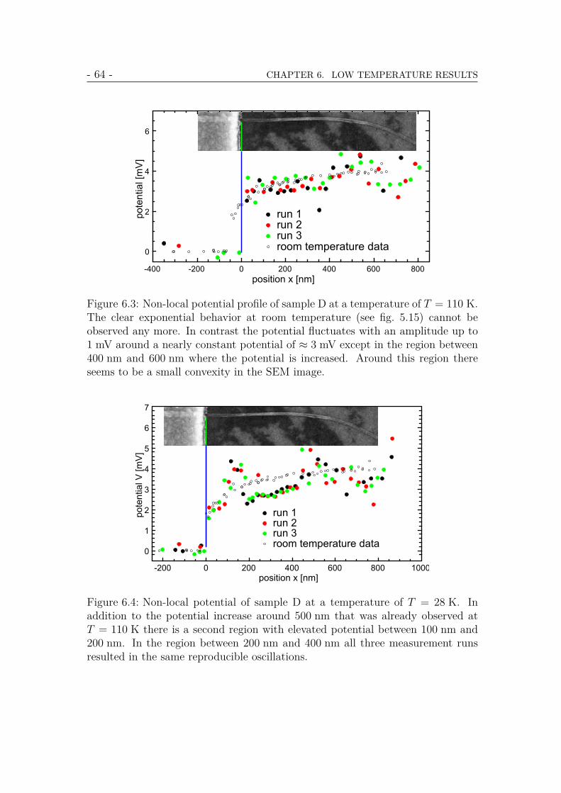
- 64 - CHAPTER 6. LOW TEMPERATURE RESULTS
Figure 6.3: Non-local potential profile of sample D at a temperature of T = 110 K.The clear exponential behavior at room temperature (see fig. 5.15) cannot beobserved any more. In contrast the potential fluctuates with an amplitude up to1 mV around a nearly constant potential of ≈ 3 mV except in the region between400 nm and 600 nm where the potential is increased. Around this region thereseems to be a small convexity in the SEM image.
Figure 6.4: Non-local potential of sample D at a temperature of T = 28 K. Inaddition to the potential increase around 500 nm that was already observed atT = 110 K there is a second region with elevated potential between 100 nm and200 nm. In the region between 200 nm and 400 nm all three measurement runsresulted in the same reproducible oscillations.
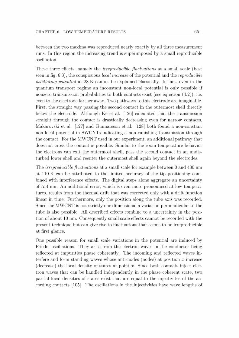
CHAPTER 6. LOW TEMPERATURE RESULTS - 65 -
between the two maxima was reproduced nearly exactly by all three measurementruns. In this region the increasing trend is superimposed by a small reproducibleoscillation.
These three effects, namely the irreproducible fluctuations at a small scale (bestseen in fig. 6.3), the conspicuous local increase of the potential and the reproducibleoscillating potential at 28 K cannot be explained classically. In fact, even in thequantum transport regime an inconstant non-local potential is only possible ifnonzero transmission probabilities to both contacts exist (see equation (4.2)), i.e.even to the electrode farther away. Two pathways to this electrode are imaginable.First, the straight way passing the second contact in the outermost shell directlybelow the electrode. Although Ke et al. [126] calculated that the transmissionstraight through the contact is drastically decreasing even for narrow contacts,Makarovski et al. [127] and Gunnarsson et al. [128] both found a non-constantnon-local potential in SWCNTs indicating a non-vanishing transmission throughthe contact. For the MWCNT used in our experiment, an additional pathway thatdoes not cross the contact is possible. Similar to the room temperature behaviorthe electrons can exit the outermost shell, pass the second contact in an undis-turbed lower shell and reenter the outermost shell again beyond the electrodes.
The irreproducible fluctuations at a small scale for example between 0 and 400 nmat 110 K can be attributed to the limited accuracy of the tip positioning com-bined with interference effects. The digital steps alone aggregate an uncertaintyof ≈ 4 nm. An additional error, which is even more pronounced at low tempera-tures, results from the thermal drift that was corrected only with a drift functionlinear in time. Furthermore, only the position along the tube axis was recorded.Since the MWCNT is not strictly one dimensional a variation perpendicular to thetube is also possible. All described effects combine to a uncertainty in the posi-tion of about 10 nm. Consequently small scale effects cannot be recorded with thepresent technique but can give rise to fluctuations that seems to be irreproducibleat first glance.
One possible reason for small scale variations in the potential are induced byFriedel oscillations. They arise from the electron waves in the conductor beingreflected at impurities phase coherently. The incoming and reflected waves in-terfere and form standing waves whose anti-nodes (nodes) at position x increase(decrease) the local density of states at point x. Since both contacts inject elec-tron waves that can be handled independently in the phase coherent state, twopartial local densities of states exist that are equal to the injectivites of the ac-cording contacts [105]. The oscillations in the injectivities have wave lengths of

- 66 - CHAPTER 6. LOW TEMPERATURE RESULTS
λ = 2πkF≈ 4 A whereby kF denotes the Fermi wavevector. Since the measured
potential is the average of the potentials of the electrodes, weighted with the in-jectivities (see equation (4.3)) the resulting potential has also a periodicity in therange of 4 A. This is well below the lateral resolution that results in apparentlyrandom oscillations depending on the exact position of the tip on the tube.
Another approach for these fluctuations is given by Makarovski et al. [127] andGunnarsson et al. [128]. The authors found significant voltages in four-pointmeasurements of SWCNTs in non-local geometry and traced it back to differentcoupling of the probes to the two orbital modes of the tube. Due to the differ-ent interaction of the two modes with the evaporated contacts, the transmissionprobabilities can be modulated differently and consequently their electrochemicalpotentials (as defined in equation (4.3)) differ from each other.
In equation (4.3) it was stated that the measured potential is independent of thecoupling strength. This results from the square of the coupling energy contributinglinearly to all Tαβ (equation (1) of ref. [105]). In the case of two independentlycontributing modes, however, the two different coupling constants cannot cancel.The measured potential depends on the coupling energies t and t to the two modesas follows (˜distinguishes the two modes.):
µ3 =
(|t|2νx1 + |t|2νx1
)µ1 +
(|t|2νx2 + |t|2νx2
)µ2
|t|2ν(x) + |t|2ν(x) (6.3)
The measured potential µ3 lies between the two potentials that could be measuredif the probe couples only to one mode.
In the present case of a movable nanocontact the coupling strengths to the twomodes can vary and consequently the measured potential deviate from each other.Due to the limited accuracy in the positioning even if one tries to measure at thesame position the coupling constants to the two modes can vary and consequentlythe potential profile seems to be irreproducible.
Both discussed reasons for the potential fluctuation, the Friedel-like oscillations aswell as the differing coupling strengths to the two orbital modes result in principlein well defined potential measurement values1 but occur at such scales that theyare not accessible with the available technique. Thus these effects cannot bedistinguished with the available data.
1The measuring error extracted from single spectroscopy curves is well below the fluctuationheight of ≈ 1 mV.

CHAPTER 6. LOW TEMPERATURE RESULTS - 67 -
The main effect, in the regions with locally increased potential, occurs at a consid-erably larger scale. Since at least at the region at about 500 nm the structure ofthe nanotube exhibits a small structural defect a connection seems to be evident.Obviously this defect does not modify the transport properties considerably atroom temperature. Non-local room temperature curves, recorded after the lowtemperature measurements, show the same exponential behavior as above men-tioned (fig. 5.15) and therefore the differences cannot be attributed to a struc-tural damage that occurred during the low temperature measurements. The roomtemperature measurements show also that the outer shells cannot be disruptedsince this would lead to a horizontal asymptote (see potential profile of sample B,fig. 5.6). In classical terms it is not clear why the measured potential decreasesagain after the defect to the value before the defect. So, this effect can be onlydiscussed in terms of quantum conductance.
For low temperature it was reported that only outer shells contribute to the trans-port properties [68], consequently the intershell conductance has to be much lowerthan determined for room temperature. A lower intershell coupling, however, givesrise to the assumption that the electrochemical potentials in the outermost andthe second shell are considerably different. If the coupling between the STM tipand the outermost shell of the tube is reduced due to structural defects the feed-back control reduces the tip-nanotube distance in order to keep a constant tunnelcurrent. The direct coupling between tip and second shell is typically negligibledue to the higher distance to the tip and the exponential behavior of the tunnelcurrent. With a decreased distance to the tip and a reduced coupling betweenoutermost shell and tip the contribution of the second shell also has to be con-sidered. So the second shell can contribute significantly to the current in the tipresulting in an increased potential.
At the second position where this effect occurs at the lower temperature of 28 Kno structural defects at all can be observed within the resolution of the SEMimage. Possible reasons for a lower coupling to the outermost shell might be somedoping impurities that deplete the local density of states as well as adsorbates onthe surface.
The last remarkable effect of the non-local low temperature measurements is thereproducible oscillating potential in the area ranging from 200 nm to 400 nm atT = 28 K. The question why irreproducible fluctuations are strongly suppressedin this area is unsolved so far. Only one outlier in this region could be observedat x = 240 nm. All other values lie close to one general oscillating curve. Theexplanation for this oscillating potential is, similar to the universal conductance

- 68 - CHAPTER 6. LOW TEMPERATURE RESULTS
Figure 6.5: Several paths of one elec-tron that hits the left scattering cen-ter. At every measurement position(two are illustrated, marked with cir-cles) the injectivity to a probe (tip) isrepresented by the interference of allpossible pathways.
fluctuations, a result of interference of several paths that included phase coherentscattering centers. The illustration in fig. 6.5 shows possible pathways after anelectron is scattered at the leftmost scattering center. At the measurement posi-tion all amplitudes of the paths that depend on the scattering cross sections sumup with appropriate phase relation. Electrons originating from different contactelectrodes form a specific interference pattern for each contact whose intensitiesrepresents the injectivities at this position. The resulting measured potential canbe calculated as in equation 4.3. Depending on the density of scattering centersand on the position of the scattering centers the potential profile exhibit irregularbut reproducible oscillations as observed.
In summary, the low temperature potential profile of sample D was measuredin local as well as in non-local geometry. The average resistivity increases withdecreasing temperature. The resistance increase can be interpreted in terms ofweak localization but within the available temperature range and precision itcannot be distinguished between 1D od 2D weak localization.
In the non-local data, however, the exponential behavior that indicates classi-cal diffusive intershell transport disappears at low temperature. Instead of thatseveral quantum conductance effects appear. Fluctuations that appear as irre-producible are a result of small scale potential variations combined with the un-certainty in the lateral position of the probe. Furthermore, regions with stronglyincreased potential can be attributed to a reduced coupling to the outermost shelland therefore the transmission probability in the second shell can contribute con-siderably. In a region at 28 K where no irreproducible fluctuations occurred anoscillating behavior was observed that can be interpreted in terms of interferenceof several electron paths similar to universal conductance fluctuations.

7 Summary
In this thesis electronic transport properties of multiwall carbon nanotubes havebeen examined. In particular, the influence of the multiple shell geometry and theimpact of structural defects on the conductance were investigated.
In order to gain access to these material parameters experimentally, MWCNTswere placed on a thin insulator surface covering a conducting layer. Metal elec-trodes with low contact resistance have been evaporated on top as source anddrain. The tip of a scanning tunneling microscope was used to localize the tubeand to act as a movable voltage probe. For this purpose the spectroscopy modewas used since it allows extracting the potential in a voltage compensated state.Due to the tunneling contact and the zero current flow the intrinsic properties arenot influenced by the voltage probe.
With this experimental setup the potential profile of the outermost shell or theelectrode where the tube is covered by metal was recorded as a function of theposition while a constant current was flowing through the tube. The contactresistance can be directly read out from the potential step at the metal tubetransition. The measurements were performed in a local as well as in a non-localgeometry at room temperature and at low temperatures.
The room temperature data were interpreted in terms of classical diffusive trans-port using a resistance model. The present model incorporates two shells wherethe second represents the effective parameters of the inner tube. It considers thefinite dimensions of the contacts and the finite total length of the tube. The modelrebuilds well the measured potential profile of a tube without obvious defects andyields additional information on the current paths over the shells and the currentdensity in the injection zone. Deviations between the model and the measureddata could be traced back to asymmetrically evaporated contacts. One main re-sult of this work is a considerably higher conductance between the shells at roomtemperature than published so far [94]. This difference was traced back to a largeimpact of the array of contacts on the tube of the previous experiments.
The resistance model could also be fitted well to the potential profile of a MWCNT
69

- 70 - CHAPTER 7. SUMMARY
with an incomplete outermost shell. The extracted parameters like intershellconductivity and intrashell resistivity are of the same order of magnitude thanthose of a tube without obvious defect. Furthermore the potential profile of a tubewith an intramolecular junction exhibited an anomaly including a change of slopethat was directly attributed to the position where the diameter changes, indicatinga transition from a metallic to a semiconducting tube. The local potential as afunction of the gate voltage does not reveal any significant gate dependency atroom temperature.
One sample, originally without obvious defect, was stretched and kinked by meansof applying a force perpendicular to the tube with the STM tip. After manipula-tion, the structure exhibited three regions with individual geometrical properties.The differences of these regions are manifested in the potential profile with dis-tinct slopes which represent different resistivities. Generally, the resistivities of allregions were increased during manipulation. The sector of the tube protruding thecontacts was not manipulated and exhibits an exponentially decreasing potentialas the model predicted. The extracted tube parameters are similar to those of theprevious samples.
Further experiments on the same sample at low temperatures revealed severaltemperature dependent effects. The potential profile in local geometry reveals anincreasing resistivity with decreasing temperature. It can be attributed to theweak localization theory and therefore indicates a decreasing amount of phasedestroying inelastic scattering.
The data recorded in non-local geometry showed several anomalies that have tobe described with quantum interference effects. In particular, it can be statedthat not only the position of the probe but also the ratio of the coupling strengthsto several modes like the orbital modes of one tube or modes of lower shells affectthe measured potential. Furthermore, oscillations in the potential profile can beattributed to the interference of several pathways that arise from scattering atinhomogeneously distributed scattering centers.

Bibliography
[1] H. P. Boehm, R. Setton, and E. Stumpp. Nomenclature and terminology ofgraphite intercalation compounds. Pure & Appl. Chem. 66: 1893 (1994).
[2] C. Frondel and U. B. Marvin. Lonsdaleite, a hexagonal polymorph of dia-mond. Nature 214: 587 (1967).
[3] H. W. Kroto, J. R. Heath, S. C. O’Brien, R. F. Curl, and R. E. Smalley.C60: Buckminsterfullerene. Nature 318: 162 (1985).
[4] W. Kratschmer, L. D. Lamb, K. Forstiropoulos, and D. R. Huffman. Solidc60: a new form of carbon. Nature 347: 354 (1990).
[5] S. Iijima. Direct observation of the tetrahedral bonding in graphitized carbonblack by high resolution electron microscopy. J. Cryst. Growth 50: 675(1980).
[6] S. Iijima. Helical microtubules of graphitic carbon. Nature 354: 56 (1991).
[7] S. Iijima and T. Ichihashi. Single-shell carbon nanotubes of 1-nm diameter.Nature 636: 603 (1993).
[8] D. S. Bethune, C. H. Klang, M. S. de Vries, G. Gorman, R. Savoy,J. Vazquez, and R. Beyers. Single-shell carbon nanotubes of 1-nm diam-eter. Nature 636: 603 (1993).
[9] A. Thess, R. Lee, P. Nikolaev, H. Dai, P. Petit, J. Robert, C. Xu, Y. H. Lee,S. G. Kim, A. G. Rinzler, D. T. Colbert, G. E. Scuseria, D. Tomanek, J. E.Fischer, and R. E. Smalley. Crystalline ropes of metallic carbon nanotubes.Science 273: 483 (1996).
[10] H. Dai, A. G. Rinzler, P. Nikolaev, A. Thess, D. T. Colbert, and R. E. Smal-ley. Single-wall nanotubes produced by metal-catalyzed disproportionation ofcarbon monoxide. Chem. Phys. Lett. 260: 471 (1996).
71

- 72 - Bibliography
[11] L. D. Landau. Zur theorie der phasenumwandlungen ii. Phys. Z. Sowjetunion11: 26 (1937).
[12] K. S. Novoselov, A. K. Geim, S. V. Morozov, D. Jiang, Y. Zhang, S. V.Dubonos, I. V. Grigorieva, and A. A. Firsov. Electric field effect in atomi-cally thin carbon films. Science 306: 666 (2004).
[13] P. R. Wallace. The band theory of graphite. Phys. Rev. 71: 622 (1946).
[14] K. S. Novoselov, A. K. Geim, S. V. Morozov, D. Jiang, M. I. Katsnelson,I. V. Girgorieva, S. V. Dubonos, and A. A. Firsov. Two-dimensional gas ofmassless dirac fermions in graphene. Nature 438: 197 (2005).
[15] Y. Zhang, Y. W. Tan, H. L. Stormer, , and P. Kim. Experimental observationof the quantum hall effect and berry’s phase in graphene. Nature 438: 201(2005).
[16] L. V. Radushkevich and V. M. Lukyanovich. O strukture ugleroda, obrazu-jucegosja pri termiceskom razlozenii okisi ugleroda na zeleznom kontakte.Zurn Fisic Chim 26: 88 (1952).
[17] From: User mstroeck on en.wikipedia; licence: Gfdl.
[18] T. Hayashi, Y. A. Kim, T. Matoba, M. Esaka, K. Nishimura, T. Tsukada,M. Endo, and M. S. Dresselhaus. Smallest freestanding single-walled carbonnanotube. Nano Letters 3: 887 (2003).
[19] S. Lebedkin, P. Schweissb, B. Renkerb, S. Malika, F. Hennrichc, M. Neu-maierc, C. Stoermerc, and M. M. Kappesa. Single-wall carbon nanotubeswith diameters approaching 6 nm obtained by laser vaporization. Carbon40: 417 (2002).
[20] C. H. Kiang. Growth of large-diameter single-walled carbon nanotubes. J.Phys. Chem. A 104: 2454 (2000).
[21] J. A. Elliott, J. K. W. Sandler, A. H. Windle, R. J. Young, , and M. S. P.Shaffer. Collapse of single-wall carbon nanotubes is diameter dependent.Phys. Rev. Lett. 92: 095501 (2004).
[22] L. Henrard, A. Loiseau, C. Journet, and P. Bernier. Study of the symmetryof single-wall nanotubes by electron diffraction. Eur. Phys. J. B 13: 661(2004).

Bibliography - 73 -
[23] P. X. Houa, C. Liua, and H. M. Cheng. Purification of carbon nanotubes.Carbon 46: 661 (2008).
[24] J. C. Charlier, X. Blase, and S. Roche. Electronic and transport propertiesof nanotubes. Rev. Mod. Phys. 79: 677 (2007).
[25] J. C. Charlier. Defects in carbon nanotubes. Acc. Chem. Res. 35: 1063(2002).
[26] A. J. Stone and D. J. Wales. Theoretical studies of icosahedral c60 and somerelated species. Chem. Phys. Lett. 128: 501 (1986).
[27] P. Lambin, A. Fonseca, J. P. Vigneron, J. B. Nagy, and A. A. Lucas. Struc-tural and electronic properties of bent carbon nanotubes. Chem. Phys. Lett.245: 85 (1995).
[28] M. Liuand and J. M. Cowley. Structures of carbon nanotubes studied byhrtem and nanodiffraction. Ultramicroscopy 53: 333 (1994).
[29] J. G. Lavina, S. Subramoney, R. S. Ruoffb, S. Berberc, and D. Tomanek.Scrolls and nested tubes in multiwall carbon nanotubes. Carbon 40: 1123(2002).
[30] P. J. F. Harris. Carbon Nanotube Science (Cambridge university press,2009).
[31] S. Agrawal, M. S. Raghuveer, H. Li, and G. Ramanath. Defect-inducedelectrical conductivity increase in individual multiwalled carbon nanotubes.Appl. Phys. Lett. 90: 193104 (2007).
[32] P. Jensen, J. Gale, , and X. Blase. Catalysis of nanotube plasticity undertensile strain. Phys. Rev. B 66: 193403 (2002).
[33] D. Orlikowski, M. B. Nardelli, J. Bernholc, and C. Roland. Theoretical stmsignatures and transport properties of native defects in carbon nanotubes.Phys. Rev. B 61: 14194 (2000).
[34] M. B. Nardelli, B. I. Yakobson, and J. Bernholc. Brittle and ductile behaviorin carbon nanotubes. Phys. Rev. Lett. 81: 4656 (1998).
[35] T. Belytschko, S. P. Xiao, G. C. Schatz, and R. S. Ruoff. Atomistic simula-tions of nanotube fracture. Phys. Rev. B 65: 235430 (2002).

- 74 - Bibliography
[36] D. H. Kim and K. J. Chang. Electron transport in telescoping carbon nan-otubes. Phys. Rev. B 66: 155402 (2002).
[37] J. Cumings and A. Zettl. Localisation and nonlinear resistance in telescop-ically extended nanotubes. Phys. Rev. Lett. 93: 086801 (2004).
[38] P. Poncharal, Z. L. Wang, D. Ugarte, and W. A. de Heer. Electrostaticdeflections and electromechanical resonances of carbon nanotubes. Science238: 1513 (1999).
[39] S. Iijima, C. Brabec, A. Maiti, and J. Bernholc. Structural flexibility ofcarbon nanotubes. J. Chem. Phys. 104: 2089 (1996).
[40] A. Loiseau, P. Launois, P. Petit, S. Roche, and J.-P. Salvetate. Understand-ing Carbon Nanotubes From Basics to Applications (Springer-Verlag Berlin,2006).
[41] J. C. Charlier, X. Gonze, and J. P. Michenaud. First-principles study of theelectronic properties of graphite. Phys. Rev. B 43: 4579 (1991).
[42] C. Bena and G. Montambaux. Remarks on the tight-binding model ofgraphene. New Journal of Physics 11: 095003 (2009).
[43] L. V. Hove. The occurrence of singularities in the elastic frequency distribu-tion of a crystal. Phys. Rev. 89: 1189 (1952).
[44] C. L. Kane and E. J. Mele. Size, shape, and low energy electronic structureof carbon nanotubes. Phys. Rev. Lett 78: 1932 (1997).
[45] X. Blase, L. X. Benedict, E. L. Shirley, and S. G. Louie. Hybridization effectsand metallicity in small radius carbon nanotubes. Phys. Rev. Lett. 72: 1878(1993).
[46] M. Ouyang, J.-L. Huang, C. L. Cheung, and C. M. Lieber. Energy gaps in’metallic’ single-walled carbon nanotubes. Science 292: 702 (2001).
[47] P. Delaney, H. J. Choi, J. Ihm, S. G. Louie, and M. L. Cohen. Brokensymmetry and pseudogaps in ropes of carbon nanotubes. Nature 391: 466(1998).
[48] L. Langer, V. Bayot, E. Grivei, J. P. Issi, J. P. Heremans, C. H. Olk, L. Stock-man, C. V. Haesendonck, and Y. Bruynseraede. Quantum transport in amultiwalled carbon nanotube. Phys Rev. Lett. 76: 479 (1996).

Bibliography - 75 -
[49] L. Langer, L. Stockman, J. P. Heremans, V. Bayot, C. Olk, C. V. Hae-sendonck, Y. Bruynseraede, and J.-P. Issi. Electrical resistance of a carbonnanotube bundle. J. Mater. Res. 9: 927 (1994).
[50] S. N. Song, X. K. Wang, R. P. H. Chang, and J. B. Ketterson. Electronicproperties of graphite nanotubules from galvanomagnetic effects. Phys. Rev.Lett. 72: 697 (1994).
[51] R. Saito, G. Dresselhaus, and M. S. Dresselhaus. Physical properties ofcarbon nanotubes (Imperial College Press, 1998).
[52] F. Triozon, S. Roche, A. Rubio, and D. Mayou. Electrical transport icarbonnanotubes: Role of disorder and helical symmetries. Phys. Rev. B 69: 121410(2004).
[53] S. Wang, M. Grifoni, and S. Roche. Anomalous diffusion and elastic meanfree path in disorder-free multiwalled carbon nanotubes. Phys. Rev. B 74:121407 (2006).
[54] B. Stojetz, C. Miko, L. Forro, and C. Strunk. Effect of band structure onquantum interference in multiwall carbon nanotubes. Phys. Rev. Lett. 94:186802 (2005).
[55] S. Frank, P. Poncharal, Z. L. Wang, and W. A. de Heer. Carbon nanotubequantum resistors. Science 280: 1744 (1998).
[56] A. Urbina, I. Echeverrıa, A. Perez-Garrido, A. Dıaz-Sanchez, and J. Abellan.Quantum conductance steps in solutions of multiwalled carbon nanotubes.Phys. Rev. Lett. 90: 106603 (2003).
[57] H. J. Li, W. G. Lu, J. J. Li, X. D. Bai, and C. Z. Gu. Multichannel ballistictransport in multiwalled carbon nanotubes. Phys. Rev. Lett. 95: 086601(2005).
[58] C. Berger, Y. Yi, Z. L. Wang, and W. A. de Heer. Multiwalled carbonnanotubes are ballistic conductors at room temperature. Appl. Phys. A 74:363 (2002).
[59] E. Brown, L. Hao, J. C. Gallop, and J. C. Macfarlane. Ballistic thermalan electrical conductance measurements on individual multiwall carbon nan-otubes. Appl. Phys. Lett. 87: 023107 (2005).

- 76 - Bibliography
[60] A. Bachtold, M. S. Fuhrer, S. Plyasunov, M. Forero, E. H. Anderson,A. Zettl, and P. L. McEuen. Scanned probe microscopy of electronic trans-port in carbon nanotubes. Phys. Rev. Lett. 84: 6082 (2000).
[61] P. J. Pablo, C. G. Navarro, J. Colchero, P. A. Serena, J. G. Herrero, andA. M. Baro. Nonlinear resistance versus length in singe-walled carbon nan-otubes. Phys. Rev. Lett. 88: 036804 (2002).
[62] Y. Yaish, J. Y. Park, S. Rosenblatt, V. Sazonova, M. Brink, and P. L.McEuen. Electrical nanoprobing of semiconducting carbon nanotubes usingan atomic force microscope. Phys. Rev. Lett. 92: 046401 (2004).
[63] R. Hobara, S. Yoshimoto, T. Ikuno, M. Katayama, N. Yamauchi, W. Wong-wiriyapan, S. Honda, I. Matsuda, S. Hasegawa, and K. Oura. Electronictransport in multiwalled carbon nanotubes contacted with patterned elec-trodes. Phys. Rev. Lett. 43: 1081 (2004).
[64] A. Stetter, J. Vancea, and C. H. Back. Determination of the intershellconductance in a multiwall carbon nanotube. Appl. Phys. Lett. 93: 172103(2008).
[65] K. Liu, P. Avouris, and R. Martel. Electrical transport in doped multiwalledcarbon nanotubes. Phys. Rev. B 63: 161404 (2001).
[66] C. Schonenberger, A. Bachtold, C. Strunk, J. P. Salvetat, and L. Forro.Interference and interaction in multi-wall carbon nanotubes. Appl. Phys. A69: 283 (1999).
[67] B. L. Al’tshuler, A. G. Aronov, and B. Z. Spivak. The aaronov-bohm effectin disordered conductors. JETP Lett. 33: 94 (1981).
[68] A. Bachtold, C. Strunk, J. Salvetat, J. Bonard, L. Forro, T. Nussbaumer,and C. Schonenberger. Aharonov-bohm oscillations in carbon nanotubes.Nature 397: 673 (1999).
[69] S. J. Tans, M. H. Devoret, H. Dai, A. Thess, R. E. Smalley, L. J. Geerligs,and C. Dekker. Anomalous diffusion and elastic mean free path in disorder-free multiwalled carbon nanotubes. Nature 386: 474 (1997).
[70] M. Bockrath, D. H. Cobden, P. L. McEuen, N. G. Chopra, A. Zettl,A. Thess, and R. E. Smalley. Single-electron transport in ropes of carbonnanotubes. Science 575: 1922 (1997).

Bibliography - 77 -
[71] A. Bezryadin, A. R. M. Verschueren, S. J. Tans, and C. Dekker. Multiprobetransport on individual single-wall carbon nanotubes. Phys. Rev. Lett. 80:4036 (1998).
[72] B. Gao, Y. F. Chen, M. S. Fuhrer, D. C. Glattli, and A. Bachtold. Four-point resistance of individual single-wall carbon nanotubes. Phys. Rev. Lett.95: 196802 (2005).
[73] M. Bockrath, D. H. Cobden, J. L. nd A. G. Rinzler, R. E. Smalley, L. Ba-lents, and P. L. McEuen. Luttinger-liquid behaviour in carbon nanotubes.Nature 397: 598 (1999).
[74] J. Appenzeller, J. Knoch, V. Derycke, R. Martel, S. Wind, , and P. Avouris.Field-modulated carrier transport in carbon nanotube transistors. Phys. Rev.Lett. 89: 126801 (2002).
[75] V. Derycke, R. Martel, J. Appenzeller, and P. Avouris. Controlling dopingand carrier injection in carbon nanotube transistors. Appl. Phys. Lett. 80:2773 (2002).
[76] M. S. Purewal, B. H. Hong, A. Ravi, B. Chandra, J. Hone, and P. Kim.Scaling of resistance and electron mean free path of single-walled carbonnanotubes. Phys. Rev. Lett 98: 186808 (2007).
[77] J. Park, S. Rosenblatt, Y. Yaish, V. Sazonova, H. Ustunel, S. Braig, T. A.Arias, P. W. Brouwer, and P. L. McEuen. Electron-phonon scattering inmetallic single walled carbon nanotubes. Nano Letters 4: 517 (2004).
[78] X. Zhou, J.-Y. Park, S. Huang, J. Liu, and P. L. McEuen. Band struc-ture, phonon scattering, and the performance limit of single-walled carbonnanotube transistors. Phys. Rev. Lett 95: 146805 (2005).
[79] M. Freitag, A. T. Johnson, S. V. Kalinin, and D. A. Bonnell. Role of defectsin electronic transport through carbon nanotube field-effect transistors. Phys.Rev. Lett. 89: 216801 (2002).
[80] S. Wang and M. Grifoni. Helicity and electron-correlation effects on trans-port properties of double-walled carbon nanotubes. Phys. Rev. Lett. 95:266802 (2005).
[81] A. Rochefort, P. Avouris, F. Lesage, and D. R. Salahub. Electrical andmechanical properties of distorted carbon nanotubes. Phys. Rev. B 60: 13824(1999).

- 78 - Bibliography
[82] M. B. Nardelli and J. Bernholc. Mechanical deformations and coherenttransport in carbon nanotubes. Phys. Rev. B 60: 16338 (1999).
[83] M. B. Nardelli, J. L. Fattebert, D. Orlikowski, C. Roland, Q. Zhao, andJ. Bernholc. Mechanical properties, defects and electronic behavior of carbonnanotubes. Carbon 38: 1703 (2000).
[84] T. Kuzumaki and Y. Mitsuda. Dynamic measurement of electrical con-ductivity of carbon nanotubes during machanical deformation by nanoprobemanipulation in transmission electron microscopy. Appl. Phys. Lett 85:1250 (2004).
[85] H. S. Jang, Y. H. Lee, H. J. Na, and S. H. Nahm. Variation in electricalresistance versus strain of an individual multiwalled carbon nanotube. J.App. Phys. 104: 114304 (2008).
[86] T. W. Tombler, C. Zhou, L. Alexeyev, J. Kong, H. Dai, L. Liu, C. S. Jayan-thi, M. Tang, and S. Y. Wu. Reversible electromechanical characteristics ofcarbon nanotubes under local-probe manipulation. Nature 405: 769 (2000).
[87] D. Bozovic, M. Bocjrath, J. H. Hafner, C. M. Lieber, and H. Park. Plasticdeformations in mechanically strained single-walled carbon nanotubes. Phys.Rev. B 67: 33407 (2003).
[88] S. Sanvito, Y.-K. Kwon, D. Tomanek, and C. J. Lambertk. Fractional quan-tum conductance in carbon nanotubes. Phys. Rev. Lett. 84: 1974 (2000).
[89] S. Roche, F. Triozon, A. Rubio, and D. Mayou. Conduction mechanismsand magnetotransport in multiwalled carbon nanotubes. Phys. Rev. B 64:121401 (2001).
[90] Y.-G. Yoon, P. Delaney, and S. G. Louie. Quantum conductance of multiwallcarbon nanotubes. Phys. Rev. B 66: 073407 (2002).
[91] A. Hansson and S. Stafstrom. Intershell conductance in multiwall carbonnanotubes. Phys. Rev. B 67: 075406 (2003).
[92] A. M. Lunde, K. Flensberg, and A. P. Jauho. Intershell resistance in mul-tiwall carbon nanotubes: a coulomb drag study. Phys. Rev. B 71: 125408(2005).
[93] P. G. Collins, M. S. Arnold, and P. Avouris. Engineering carbon nanotubesand nanotube circuits using electrical breaktown. Science 292: 706 (2001).

Bibliography - 79 -
[94] B. Bourlon, C. Miko, L. Forro, D. C. Glattli, and A. Bachtold. Determi-nation of the intershell conductance in multiwalled carbon nanotubes. Phys.Rev. Lett. 93: 176806 (2004).
[95] F. W. K. Katayamaa and K. Gamoa. Contact resistance of multiwall carbonnanotubes. Microelectron. Eng. 67: 853 (2003).
[96] D. Mann, A. Javey, J. Kong, Q. Wang, and H. Dai. Ballistic transportin metallic nanotubes with reliable pd ohmic contacts. Nano Lett. 3: 1541(2003).
[97] H. Dai, E. W. Wong, and C. M. Lieber. Probing electrical transport innanomaterials: conductivity of individual carbon nanotubes. Science 272:523 (1996).
[98] W. F. Brinkman and R. C. Dynes. Tunneling conductance of asymmetricalbarriers. J. App. Phys. 41: 1915 (1970).
[99] A. Stetter. Leitfahigkeitsmessungen an kohlenstoffnanororchen mit be-weglichen nanokontakten. Diplomarbeit, Universitat Regensburg (2006).
[100] A. J. Babic, J. Furer, M. Iqbal, and C. Schonenberger. Suitability of carbonnanotubes grown by chemical vapour deposition for electrical devices. AIP-Proceedings 723: 574 (2004).
[101] A. Javey, J. Guo, Q. Wang, M. Lundstrom, and H. Dai. Ballistic carbonnanotube field-effect transistors. Nature 424: 654 (2003).
[102] Z. Chen, J. Appenzeller, J. Knoch, Y. Lin, and P. Avouris. The role ofmetal-nanotube contact in the performance of carbon nanotube field-effecttransistors. Nano Lett. 5: 1497 (2005).
[103] N. Nemec, D. Tomanek, and G. Cuniberti. Contact dependence of carrierinjection in carbon nanotubes: an an initio study. Phys. Rev. Lett. 96:076802 (2007).
[104] Discussion with prof. jascha repp.
[105] T. Gramespacher and M. Buttiker. Nanoscopic tunneling contacts on meso-scopic multiprobe conductors. Phys. Rev. B 56: 13026 (1997).
[106] M. Buttiker. Four-terminal phase coherent resistance. Phys. Rev. Lett 57:1761 (1986).

- 80 - Bibliography
[107] M. Buttiker. Symmetry of electrical conduction. IBM J. Res. Dev. 32: 317(1988).
[108] S. Datta. Electronic transport in mesoscopic systems (Cambridge universitypress, 2007), 7. edition.
[109] K. Shabrawy, K. Maharatna, D. M. Bagnall, and B. M. Al-Hashimi. Mod-eling swcnt band-gap and effective mass variation using a monte carlo ap-proach. IEEE Trans. Nano. (2009).
[110] J. M. Cowley and S. D. Packard. Coherent nanodiffraction from phase ob-jects: carbon nanotubes. Ultramicroscopy 63: 39 (1996).
[111] C. H. Kiang, M. Endo, P. M. Ajayan, G. Dresselhaus, and M. S. Dresselhaus.Size effects in carbon nanotubes. Phys. Rev. Lett. 81: 1869 (1998).
[112] W. Primak and L. H. Fuchs. Electrical conductivities of natural graphitecrystals. Phys. Rev. 95: 22 (1954).
[113] K. Matsubara, K. Sugihara, and T. Tsuzuku. Electrical resistance in the cdirection of graphite. Phys. Rev. B 41: 969 (1990).
[114] H. Schmidt, T. Ludtke, P. Barthold, and R. J. Haug. Mobilities and scat-tering times in decoupled graphene monolayers. Phys. Rev. B 81: 121403(2010).
[115] L. W. Nagel and D. Pederson. Spice (simulation program with integratedcircuit emphasis). Technical Report UCB/ERL M382, EECS Department,University of California, Berkeley (1973).
[116] Z. Yao, H. C. Postma, L. Balents, and C. Dekker. Carbon nanotube in-tramolecular junctions. Nature 402: 273 (1999).
[117] S. Paulson, M. R. Falvo, N. Snider, A. Helser, T. Hudson, A. Seeger, R. M.Taylor, R. Superfine, and S. Washburn. In situ resistance measurements ofstrained carbon nanotubes. Appl. Phys. Lett. 75: 2936 (1999).
[118] M. BuongiornoNardelli, B. I. Yakobson, and J. Bernholc. Mechanism ofstrain release in carbon nanotubes. Phys. Rev. B 57: R4277 (1998).
[119] M. J. Biercuk, N. Mason, J. M. Chow, and C. M. Marcus. Locally addressabletunnel barriers within a carbon nanotube. Nano Lett. 4: 2499 (2004).

Bibliography - 81 -
[120] D. Bozovic, M. Bockrath, J. H. Hafner, C. M. Lieber, H. Park, and M. Tin-kham. Electronic properties of mechanically induced kinks in single-walledcarbon nanotubes. Appl. Phys. Lett. 78: 3693 (2001).
[121] J. Cao, Q. Wang, and H. Dai. Electromechanical properties of metallic,quasimetallic, and semiconducting carbon nanotubes under stretching. Phys.Rev. Lett. 90: 157601 (2003).
[122] L. Yang and J. Han. Electronic structure of deformed carbon nanotubes.Phys. Rev. Lett. 85: 154 (2000).
[123] E. Graugnard, P. J. de Pablo, B. Walsh, A. W. Ghosh, S. Datta, andR. Reifenberger. Temperature dependence of the conductance of multiwalledcarbon nanotubes. Phys. Rev. B 64: 125407 (2001).
[124] C. L. Kane and M. P. A. Fisher. Transmission through barriers and resonanttunneling in an interacting one-dimensional electron gas. Phys. Rev. B 46:15233 (1992).
[125] P. A. Lee and T. V. Ramakrishnan. Disordered electronic systems. Rev.Mod. Phys. 57: 287 (1985).
[126] S. H. Ke, W. Yang, and H. U. Baranger. Nanotube-metal junctions: 2- and3-terminal electrical transport. J. Chem. Phys. 124: 124 (2006).
[127] A. Makarovski, A. Zhukov, J. Liu, and G. Finkelstein. Four-probe measure-ments of carbon nanotubes with narrow metal contacts. Phys. Rev. B 76:161405 (2007).
[128] G. Gunnarsson, J. Trbovic, and C. Schonenberger. Large oscillating nonlocalvoltage in multiterminal single-wall carbon nanotube devices. Phys. Rev. B77: 201405 (2008).


Acknowledgement - Danksagung
In der Experimentalphysik ist eine Doktorarbeit ohne Hilfe und Zusammenarbeitundenkbar. Neben vielen anderen trugen vor allem auch die folgenden Personenzum Gelingen dieser Arbeit bei.Bei Prof. Dr. Christian Back mochte ich mich einerseits fur die interessanteAufgabenstellung bedanken, auch wenn sich das Thema letztendlich weit vomursprunglich geplanten wegentwickelt hat und so nichts mehr mit Spinphanomenenzu tun hatte. Andererseits mochte ich mich auch fur die Betreuung und denangenehmen Umgang miteinander bedanken.Mein direkter Betreuer Dr. Johann Vancea half mir mit seiner großen Erfahrungbei Experimenten und ermunterte mich meine Ergebnisse und Uberlegungen of-fensiver zu verteidigen.Fur die angenehme Zusammenarbeit mit meinem Laborkollegen Florian Freundmochte ich mich ebenso bedanken. Das gleiche gilt fur ”unsere” Diplomanden undZulassungskandidaten (Michael, Gerhard, Sebastian, Gerhard, Christian).Unser Lehrstuhltechniker Tobias Stockl half mit seiner großen Erfahrung bei derKonstruktion von neuen Bauteilen. Besonderer Dank gebuhrt ihm fur seineschnelle Eisatzbereitschaft wenn kurzfristig Bauteile angepasst oder repariert wer-den mussten.Allen Mitgliedern des Lehrstuhls Back danke ich fur die angenehme Zusammenar-beit und Unterstutzung wenn Not am Mann war.Als Fachmann fur mesoskopische Systeme war Prof. Dr. Christoph Strunk furmich immer wieder ein kompetenter Ansprechpartner wenn ich meine Ergebnissenicht alleine interpretieren konnte. Fur die Zeit und die Bereitschaft mir zu helfenmochte ich mich bedanken.All meine Proben habe ich im Reinraum von Prof. Dr. Dieter Weiss hergestellt.Fur den Zugang dazu mochte ich mich bedanken.Dieter Riedl und Max Simmel aus der Elektronikwerkstatt danke ich fur diemaßgeschneiderten Elektroniken und vor allem fur das Reparieren von Geraten
83

- 84 - Bibliography
die der Hersteller selbst als nicht mehr reparabel einstufte.
Außerdem mochte ich mich bei Manuel, Sebi, Oko, Julia, Sophia und insbeson-dere Steffi fur die angenehme Zeit z.B. beim Teetrinken bedanken, und fur dieaufbauenden Worte, wenn schon wieder mal eine Probe kaputt war.
Nicht zuletzt mochte ich mich auch bei meinen Eltern fur die Unterstutzungwahrend meines Studiums und meiner Promotion bedanken.


![p200306-501.ppt [호환 모드]Making nanotubes Electric arc - batch reactor scaleup - continuous reactor batch reactor operation cathode deposit multiwall nanotubes from batch arc](https://static.fdocuments.net/doc/165x107/5e89583087e7cc6aee107903/p200306-501ppt-eeoe-making-nanotubes-electric-arc-batch-reactor-scaleup.jpg)

![Preparation of multiwall carbon nanotubes (MWCNTs ...€¦ · polymeric reinforcement[1–4].Theypossessoutstandingelec-trical, mechanical and thermal properties compared to conven-tional](https://static.fdocuments.net/doc/165x107/5f0d06527e708231d4384d8d/preparation-of-multiwall-carbon-nanotubes-mwcnts-polymeric-reinforcement1a4theypossessoutstandingelec-trical.jpg)