
AND9972 - 3-phase Inverter Power Module 1200 V SPM® 31 ...
32
© Semiconductor Components Industries, LLC, 2019 December, 2019 − Rev. 1 1 Publication Order Number: AND9972/D AND9972 3-phase Inverter Power Module 1200 V SPM ) 31 Series Application Note INTRODUCTION This application note provides practical guidelines for designing with the SPM 31 Series power modules. This series of Intelligent Power Modules (IPM) for 3−phase motor drives contains a three−phase inverter stage, gate drivers and a thermistor (Optional). Design Concept The SPM 31 design objective is to provide a minimized package and a low power consumption module with improved reliability. It is achieved by applying new gate−driving High−Voltage Integrated Circuit (HVIC), a new Insulated−Gate Bipolar Transistor (IGBT) of advanced silicon technology, and improved Direct Bonded Copper (DBC) substrate based on transfer mold package. The SPM 31 achieves reduced board size and improved reliability compared to existing discrete solutions. Target applications are inverter motor drives for industrial use, such as commercial air conditioners, general−purpose inverters and servo motors. The temperature sensing function of SPM 31 products are implemented in the LVIC to enhance the system reliability and isolated optional thermistor is available. The analog voltage proportional to the temperature of the LVIC and integrated thermistor temperature in module are provided for monitoring the module temperature and necessary protections against over−temperature situations. Figure 1 shows the package outline structure. Figure 1. External View and Internal Structure of SPM 31 Key Features • 1200 V / 5, 10, 20 A, three phase IGBT inverter including control ICs for gate driving and protections • Very low thermal resistance by adopting DBC substrate • Easy PCB layout thanks to built−in bootstrap circuits • Open emitter configuration for easy monitoring of each phase current sensing • Single−grounded power supply thanks to built−in HVICs and bootstrap operations • Built−in temperature sensing function by LVIC and optional NTC • Isolation Rating of 2500 Vrms / min www. onsemi.com APPLICATION NOTE
Transcript of AND9972 - 3-phase Inverter Power Module 1200 V SPM® 31 ...
© Semiconductor Components Industries, LLC, 2019
December, 2019 − Rev. 11 Publication Order Number:
AND9972/D
AND9972
3-phase Inverter PowerModule 1200 V SPM� 31Series Application Note
INTRODUCTIONThis application note provides practical guidelines for
designing with the SPM 31 Series power modules.This series of Intelligent Power Modules (IPM) for
3−phase motor drives contains a three−phase inverter stage,gate drivers and a thermistor (Optional).
Design ConceptThe SPM 31 design objective is to provide a minimized
package and a low power consumption module withimproved reliability. It is achieved by applying newgate−driving High−Voltage Integrated Circuit (HVIC), anew Insulated−Gate Bipolar Transistor (IGBT) of advancedsilicon technology, and improved Direct Bonded Copper(DBC) substrate based on transfer mold package. TheSPM 31 achieves reduced board size and improvedreliability compared to existing discrete solutions. Targetapplications
are inverter motor drives for industrial use, such ascommercial air conditioners, general−purpose inverters andservo motors. The temperature sensing function of SPM 31products are implemented in the LVIC to enhance the systemreliability and isolated optional thermistor is available. Theanalog voltage proportional to the temperature of the LVICand integrated thermistor temperature in module areprovided for monitoring the module temperature andnecessary protections against over−temperature situations.Figure 1 shows the package outline structure.
Figure 1. External View and Internal Structure of SPM 31
Key Features• 1200 V / 5, 10, 20 A, three phase IGBT inverter including
control ICs for gate driving and protections• Very low thermal resistance by adopting DBC substrate
• Easy PCB layout thanks to built−in bootstrap circuits
• Open emitter configuration for easy monitoring of eachphase current sensing
• Single−grounded power supply thanks to built−in HVICsand bootstrap operations
• Built−in temperature sensing function by LVIC andoptional NTC
• Isolation Rating of 2500 Vrms / min
www.onsemi.com
APPLICATION NOTE

AND9972
www.onsemi.com2
PRODUCT DESCRIPTION
Ordering Information
N F A M 2 0 1 2 L 5 B T
Temperature OptionBlank: W/O NTC thermistorT: Built−in NTC thermistor
Lead Forming / LengthB: Short Lead / Flat / Flat N
Silicon TechnologyL4: Field Stop 4 IGBTL5: FS II IGBTVoltage Rating
65: 650 V12: 1200 VCurrent Rating
50: 50 A RatingPackageM: SPM 31Topology
A: InverterProduct GroupF: Intelligent Power Module, IPM
Figure 2. Ordering Information
Product Line−upTable 1 shows the basic line up without package
variations. Online loss and temperature simulation tool,
Motion Control Design Tool is recommended to find out theright IPM product for the desired application. For packagedrawing, please refer to Chapter Package Outline.
Table 1. PRODUCT LINE−UP
Target Application Device IGBT Rating Motor Rating (Note 1) Isolation Voltage
Air Conditioners, Industrial Motor,
General−purpose inverters,Servo motors
NFAM0512L5B(T) (Note 2) 5 A / 1200 V 0.75 kW VISO = 2500 Vrms(Sine 60 Hz, 1−min
All Shorted Pins Heat Sink)NFAM1012L5B(T) (Note 2) 10 A / 1200 V 1.5 kW
NFAM2012L5B(T) 20 A / 1200 V 2.2 kW
1. These motor ratings are general ratings, so it can be changed by the operating conditions.2. Under development.
Internal Circuit DiagramThree bootstrap circuits generate the voltage needed for
driving the high−side IGBTs. The boost diodes are internalto the part and sourced from VDD (15 V). There is aninternal level shift circuit for the high−side drive signalsallowing all control signals to be driven directly from GNDlevels common with the control circuit such as themicrocontroller without requiring external isolation withopto−couplers.
Major differences between SPM 31 T version and normalversion are shown on pins 38 and 39 of the internal circuitdiagram as shown in Figure 3. The T version has built−inNTC that senses the temperature of the power chip. Innormal version, NTC is not built in. Both T version andNormal version function as conventional functions LVICtemperature sensing signal is output from the VTS pin.

AND9972
www.onsemi.com3
HIN(U) (6)HVIC1
VDD(UH) (4)
VB(U) (3)
VS(U) (1)
LIN(V) (22)
VTS (20)
LIN(U) (21)
VTH (38)
U (36)
P (37)
V (35)
W (34)
NU (33)
NV (32)
NW (31)
RTH (39)
VS
HIN
VDD
VB
VSS
HOUT
HIN(V) (12)HVIC2
VDD(VH) (10)
VB(V) (9)
VS(V) (7)
VS
HIN
VDD
VB
VSS
HOUT
HIN(W) (18)HVIC3
VDD(WH) (16)
VB(W) (15)
VS(W) (13)
VS
HIN
VDDVB
VSS
HOUT
LVIC
OUT(U)
OUT(V)
OUT(W)
LIN(W) (23)
VFO (24)
CFOD (25)
CIN (26)
VSS (27)
VDD(L) (28)
VTS
LIN(U)
LIN(V)
LIN(W)
VFO
CFOD
CIN
VSS
VDD
Integrated bootstrap circuits High side gate drivers NTC thermistor (Optional)
Field Stop Trench II IGBT// Fast Recovery Diode
Low side gate driver
VB(X), VS(X)Floating supply for high
side X−phase IGBT control
VDD(XH)Supply for High side
X−phase driver
HIN(X)PWM input port for high
side X−phase
VTSTemperature sensing
output
LIN(X)PWM input port for low
side X−phase
VFOFault signal output
CFODDuration time control for
fault signal
CINOver current protection
input
VSSDriver GND
VDD(L)Supply for low side driverand low side IGBT control
XTHOptional NTC thermistor for temperature sensing
PPositive Dcbus input
UU phase output
VV phase output
WW phase output
NUU phase low sideemitter
NVV phase low sideemitter
NWW phase low sideemitter
Figure 3. Internal Equivalent Circuit Diagram
NTC Thermistor
AND9972
www.onsemi.com4
(39)
RT
H
(38)
VT
H
(37)
P
(36)
U
(35)
V
(35)
W
(33)
NU
(32)
NV
(1)
VS
(U)
(3)
VB
(U)
(4)
VD
D(U
H)
(6)
HIN
(U)
(9)
VB
(V)
(7)
VS
(V)
(13)
VS
(W)
(15)
VB
(W)
(16)
VD
D(W
H)
(10)
VD
D(V
H)
(12)
HIN
(V)
(18)
HIN
(W)
(20)
VT
S(2
1) L
IN(U
)(2
2) L
IN(V
)(2
3) L
IN(W
)(2
4) V
FO
(25)
CF
OD
(26)
CIN
(27)
VS
S(2
8) V
DD
(L)
(31)
NW
Figure 4. Package Top−View and Pin Assignment
Table 2. NUMBERS, NAMES AND DUMMY PINS
Pin Numbers Names Description
1 VS(U) High−Side Bias Voltage GND for U Phase IGBT Driving
(2) − Dummy
3 VB(U) High−Side Bias Voltage for U Phase IGBT Driving
4 VDD(UH) High−Side Bias Voltage for U Phase IC
(5) − Dummy
6 HIN(U) Signal Input for High−Side U Phase
7 VS(V) High−Side Bias Voltage GND for V Phase IGBT Driving
(8) − Dummy
9 VB(V) High−Side Bias Voltage for V Phase IGBT Driving
10 VDD(VH) High−Side Bias Voltage for V Phase IC
(11) − Dummy
12 HIN(V) Signal Input for High−Side V Phase
13 VS(W) High−Side Bias Voltage GND for W Phase IGBT Driving
(14) − Dummy
15 VB(W) High−Side Bias Voltage for W Phase IGBT Driving
16 VDD(WH) High−Side Bias Voltage for W Phase IC
(17) − Dummy
18 HIN(W) Signal Input for High−Side W Phase
(19) − Dummy
20 VTS Voltage Output for LVIC Temperature Sensing Unit
21 LIN(U) Signal Input for Low−Side U Phase
22 LIN(V) Signal Input for Low−Side V Phase
23 LIN(W) Signal Input for Low−Side W Phase
24 VFO Fault Output

AND9972
www.onsemi.com5
Table 2. NUMBERS, NAMES AND DUMMY PINS
Pin Numbers DescriptionNames
25 CFOD Capacitor for Fault Output Duration Selection
26 CIN Input for Over Current Protection
27 VSS Low−Side Common Supply Ground
28 VDD(L) Low−Side Bias Voltage for IC and IGBTs Driving
(29) − Dummy
(30) − Dummy
31 NW Negative DC−Link Input for W Phase
32 NV Negative DC−Link Input for V Phase
33 NU Negative DC−Link Input for U Phase
34 W Output for W Phase
35 V Output for V Phase
36 U Output for U Phase
37 P Positive DC−Link Input
38 VTH Thermistor Bias Voltage (T) / Not Connection
39 RTH Series Resister for Thermistor (Temperature Detection) *Optional for T
3. Pins of ( ) are the dummy for internal connection. These pins should be no connection.
Detailed Pin Definition and NotificationPins: VB(U) − VS(U), VB(V) − VS(V), VB(W) − VS(W)• High−side bias voltage pins for driving the IGBT /
high−side bias voltage ground pins for driving the IGBTs.• VB(U), VB(V), VB(W) are integrated bootstrap diode
cathode pins.• These are drive power supply pins for providing gate
drive power to the high−side IGBTs.• The virtue of the ability to bootstrap the circuit scheme is
that no external power supplies are required for thehigh−side IGBTs. Each bootstrap capacitor is chargedfrom the VDD supply during ON state of thecorresponding low−side IGBT and Diode.
• To prevent malfunctions caused by noise and ripple in thesupply voltage, a low−ESR, a low−ESL filter capacitorshould be mounted very close to these pins.
Pins: VDD(L), VDD(UH), VDD(VH), VDD(WH)• Low−side bias voltage pins / high−side driver bias voltage
pins.• This is control supply pins for the built−in ICs.
• These four pins should be connected externally.
• To prevent malfunctions caused by noise and ripple in thesupply voltage, a low−ESR, low−ESL filter capacitorshould be mounted very close to these pins.
Pin: VSS• Control signal ground pin.
• This is supply ground pin for the built−in ICs.
• Important! To avoid noise influences, the main powercircuit current should not be allowed to blow through thispin.
Pins: HIN(U), HIN(V), HIN(W), LIN(U), LIN(V), LIN(W)• Signal input pins.
• These pins control the operation of the built−in IGBTs.
• They are activated by voltage input signals. The terminalsare internally connected to a Schmitt−trigger circuitcomposed of 5 V−class CMOS.
• The signal logic of these pins is active high. The IGBTassociated with each of these pins is turned on.
• ON when a sufficient logic voltage is applied to thesepins.
• The wiring of each input should be as short as possible toprotect the SPM 31 against noise influences.
• To prevent signal oscillations, an RC coupling asillustrated in Figure 28 is recommended.
Pin: CIN• Over−current and short−circuit detection input pin.
• The current sensing shunt resistor should be connectedbetween the pin CIN and the low−side ground pin VSS todetect over or short circuit current.
• The shunt resistor should be selected to meet the detectionlevels matched for the specific application.
• An RC filter should be connected to the CIN pin toeliminate noise.
• The connection length between the shunt resistor and CINpin should be minimized.

AND9972
www.onsemi.com6
Pin: VFO• Fault output pin.
• This is the fault output alarm pin. An active low output isgiven on this pin for a fault state condition in the SPM 31.
• The alarm conditions are: Short−Circuit CurrentProtection (SCP), and low−side bias Under−Voltage LockOut (UVLO).
• The VFO output is open drain configured. The VFOsignal line should be pulled to the 5 V logic power supplywith approximately 10 k� resistance.
Pin: CFOD• Fault output duration time control pin.
• The fault−out pulse width time depends on thecapacitance value of CFOD.
Pin: VTH, RTH (Optional for T type)• For case temperature (Tc) detection, this pin should be
connected to an external series resistor.• The external series resistor should be selected to meet the
detection range matched for the specification of eachapplication (for details, refer to Figure 22).
Pin: VTS• Analog temperature sensing output pin.
• This is to indicate the temperature of LVIC with analogvoltage. LVIC itself creates some power loss, but mainlyheat generated from the IGBTs will increase thetemperature of the LVIC.
• VTS versus temperature characteristics is illustrated inFigure 17.
Pin: P• Positive DC−link pin.
• This is the DC−link positive power supply pin of theinverter.
• It is internally connected to the collectors of the high−sideIGBTs.
• To suppress surge voltage caused by the DC−link wiringor PCB pattern inductance, connect a smoothing filtercapacitor close to this pin (tip: metal film capacitor istypically used).
Pins: NU, NV, NW• Negative DC−link pins.
• These are the DC−link negative power supply pins (powerground) of the inverter.
• These pins are connected to the low−side IGBT emittersof each phase.
• These pins are used to one shunt or three shunt resistor.
Pins: U, V, W• Inverter power output pins.
• Inverter output pins for connecting to the inverter load(e.g. motor).

AND9972
www.onsemi.com7
PACKAGE
Package StructureSince heat dissipation is an important factor limiting the
power module’s current capability, the heat dissipationcharacteristics of a package are important in determining theperformance. A trade−off exists among heat dissipationcharacteristics, package size, and isolation characteristics.The key to good package technology lies in the optimizationpackage size while maintaining outstanding heat dissipationcharacteristics without compromising the isolation rating.
In SPM 31, technology was developed with DBCsubstrate that resulted in excellent heat dissipationcharacteristics. Power chips are attached directly to the DBCsubstrate. This technology is applied SPM 31, achievingimproved reliability and heat dissipation.
Figure 5 and Figure 6 show the package outline and thecross−sections of the SPM 31 package.
Figure 5. Vertical Structure for Heat Dissipation and Distance for Isolation
Figure 6. Package Structure and Cross Section for SPM 31
AND9972
www.onsemi.com8
Marking Specification Base on NFAMxx12L5BT
Note 4Note 5
Note 6 Note 7
NOTES:4. No.1 pin identification mark5. Specific Device code6. Lot / Serial7. 2D code
Figure 7. Marking Specification Base on NFAMxx12L5BT
Package Outline
Unit: mm
Figure 8. NFAM2012L5BT

AND9972
www.onsemi.com10
PRODUCT SYNOPSIS
This section discusses electrical specification, characteristics and mechanical characteristics.
Absolute Maximum Rating (Tc = 25°C, unless otherwise specified)
ABSOLUTE MAXIMUM RATING (Tc = 25°C, unless otherwise specified)
Symbol Parameter Conditions Rating Unit
INVERTER PART (BASE ON NFAM2012L5BT)
VPN Supply Voltage Applied between P − NU, NV, NW 900 V
VPN(surge) Supply Voltage (Surge) Applied between P − NU, NV, NW 1000
Vces Collector – Emitter Voltage 1200
±Ic Each IGBT Collector Current Tc = 25°C, Tj ≤ 150°C (Note 8) 20 A
±Icp Each IGBT Collector Current (Peak) Tc = 25°C, Tj ≤ 150°C, Under 1 ms PulseWidth
40
Pc Collector Dissipation Tc = 25°C per One Chip 125 W
TJ Operating Junction Temperature (Note 8) −40~150 °C
CONTROL PART
VDD Control Supply Voltage Applied between VDD(XX) − VSS 20 V
VBS High−Side Control Bias Voltage Applied between VB(X) − VS(X) 20
VIN Input Signal Voltage Applied between HIN(X), LIN(X) − VSS −0.3~VDD
VFO Fault Output Supply Voltage Applied between VFO − VSS −0.3~VDD
IFO Fault Output Current Sink Current at VFO Pin 2 mA
VCIN Current Sensing Input Voltage Applied between CIN − VSS −0.3~VDD V
BOOTSTRAP DIODE PART
VRRM Maximum Repetitive Reverse Voltage 1200 V
CBOOT Allowable Max. Bootstrap Capacitor Tj ≤ 150°C 470 �F
TOTAL SYSTEM
VPN(PROT) Self−Protection Supply Voltage Limit(Short−Circuit Protection Capability)
VDD(XX), VB(X) = 13.5~16.5 V, Tj = 150°C,(Non−Repetitive, <2 �s)
800 V
Tc Module Case Operation Temperature See Figure 10 −40~125 °C
Tstg Storage Temperature −40~125
Viso Isolation Voltage 60 Hz, Sinusoidal, 1−Minute, Connect Pinsto Heat Sink
2500 Vrms
Stresses exceeding those listed in the Maximum Ratings table may damage the device. If any of these limits are exceeded, device functionalityshould not be assumed, damage may occur and reliability may be affected.8. These values had been made on acquisition by the calculation considered to design factor. The maximum junction temperature rating of
power chips integrated within the SPM 31 products are 150°C.
THERMAL RESISTANCE
Symbol Parameter Conditions Min Typ Max Unit
Rth(j−c)Q Junction to Case Thermal Resistance(Note 9)
Inverter IGBT Part (per 1/6 Module) − − 1.0 °C/W
Rth(j−c)F Inverter FWDi Part (per 1/6 Module) − − 1.2
9. For the measurement point of case temperature (TC), please refer Figure 10.
AND9972
www.onsemi.com11
Figure 10. Case Temperature (Tc) Detecting Point
(16) VDD(WH)(18) HIN(W)
(20) VTS(21) LIN(U)(22) LIN(V)(23) LIN(W)(24) VFO(25) CFOD(26) CIN(27) VSS(28) VDD(L)
(1) VS(U)(3) VB(U)
(39) RTH
(38) VTH
(37) P
(36) U
(35) V
(34) W
(33) NU
(32) NV
(31) NW
15.4
25.7
(7) VS(V)(9) VB(V)
(4) VDD(UH)(6) HIN(U)
(13) VS(W)(15) VB(W)
(10) VDD(VH)(12) HIN(V)
Case Temperature (Tc)Detecting Point
Electrical Characteristic (Tc = 25°C, unless otherwise specified)
ELECTRICAL CHARACTERISTIC (TC = 25°C unless otherwise noted)
Symbol Parameter Test Condition Min Typ Max Unit
INVERTER PART (BASE ON NFAM2012L5BT)
VCE(sat) Collector–Emitter Saturation Voltage
VDD, VBS = 15 V,yIN(X) = 5 V
Ic = 20 A, Tj = 25°C
− 1.85 2.45 V
VF FWDi Forward Voltage yIN(X) = 0 V If = 20 A, Tj = 25°C
− 1.85 2.35
ton Switching Times (High Side) (Note 10)
VPN = 600 V, VDD = 15 V, VBS = 15 V, Ic = 20 A, Tj = 25°C, IN = 0 V ↔ 5 V, Inductive LoadSee Figure 11
0.80 1.40 2.00 �s
tc(on) − 0.30 0.60
toff − 1.90 2.70
tc(off) − 0.20 0.60
trr − 0.40 −
ton Switching Times (Low Side) (Note 10)
0.90 1.50 2.10
tc(on) − 0.30 0.60
toff − 2.00 2.80
tc(off) − 0.20 0.60
trr − 0.40 −
Ices Collector – Emitter Leakage Current Vce = Vces, Tj = 25°C − − 1 mA
BOOTSTRAP CIRCUIT PART
VF Forward Voltage If = 0.1 A, Tj = 25°C 3.4 4.6 5.8 V
RBOOT Bootstrap Resistor If = 0.1 A, Tj = 25°C 30 38 46 �
AND9972
www.onsemi.com12
ELECTRICAL CHARACTERISTIC (TC = 25°C unless otherwise noted) (continued)
Symbol UnitMaxTypMinTest ConditionParameter
CONTROL PART
IQDDH Quiescent VDD Supply Current VDD(xH) = 15 V, HIN(X), LIN(X) = 0 V
VDD(xH) − VSS − − 0.30 mA
IQDDL Quiescent VDD Supply Current VDD(L) = 15 V, HIN(X), LIN(X) = 0 V
VDD(L) − VSS − − 3.50
IQBS Quiescent VBS Supply Current ofEach Phase
VB(X) − VS(X) = 15 V, HIN (X) = 0 V − − 0.30
VFOH Fault Output Voltage CIN = 0 V, Pulled up to 5 V by 10 k� 4.9 − − V
VFOL CIN = 1 V, Pulled up to 5 V by 10 k� − − 0.95
VCIN(ref) Short−Circuit Trip Level VDD = 15 V CIN − VSS 0.46 0.48 0.50
UVDDD Supply Circuit, Under−Voltage Protection
Detection Level 10.3 − 12.5
UVDDR Reset Level 10.8 − 13.0
UVBSD Detection Level 10.0 − 12.0
UVBSR Reset Level 10.5 − 12.5
tFOD Fault−Out Pulse Width CFOD = 22 nF 1.6 2.4 − ms
VTS Temperature output VDD(L) = 15 V, VTS – VSS = 10 nF,TLVIC = 25°C
0.905 1.030 1.155 V
VIN(ON)) ON Threshold Voltage Applied between HIN(X), LIN(X) − VSS − − 2.6
VIN(OFF) OFF Threshold Voltage 0.8 − −
Product parametric performance is indicated in the Electrical Characteristics for the listed test conditions, unless otherwise noted. Productperformance may not be indicated by the Electrical Characteristics if operated under different conditions.10. ton and toff include the propagation delay time of the internal drive IC. tc(on) and tc(off) are the switching time of IGBT itself under the given
gate driving condition internally. For the detail information, please see and Figure 11.11. Short−circuit current protection is functioning only at low side.
One−Leg Diagram of SPM 31
VDD(L)
LIN(X)
VSS
LO
P
N
Inducotor
300 V
15V
SwitchingPulse
SwitchingPulse
VDD(XH)
HIN(X)
VSS
VB(X)
HO
VS(X)
Inducotor
Line strayInductance < 100 nH
Line stray Inductance < 100 nH
15 V Only for lowside switching
OUT
HIN(X)LIN(X)
ICx
vCEx10% ICx10% VCEx 10% ICx
90% I Cx
toff ton
tc(off) tc(on)
10% VCEx
trr
100% ICx
VIN(OFF)VIN(ON)
Turn off switching
Figure 11. Switching Evaluation Circuit and Switching Time Definition

AND9972
www.onsemi.com13
Recommended Operating Conditions (Base on NFAM2012L5B(T))
RECOMMENDED OPERATING CONDITIONS (Base on NFAM2012L5B(T))
Symbol Parameter Condition Min Typ Max Unit
VPN Supply Voltage Applied between P − Nx − 600 800 V
VDD Gate Driver Supply Voltages
Applied between VDD(XH) − VSS 13.5 15.0 16.5
VBS Applied between VB(X) − VS(X) 13.0 15.0 18.5
dVDD/dt, dVBS/dt Control Supply Variation −1 − 1 V/�s
DT Dead Time Turn−off to Turn−on (external) 3 − − �s
fPWM PWM Input Signal − 1 − 20 kHz
Io Allowable r.m.s Current VPN = 600 V, VDD, VBS = 15 V, P.F = 0.8, Tc ≤ 125°C, TJ ≤ 150°C
fPWM = 5 kHz − − 18.1 Arms
fPWM = 15 kHz − − 9.4
PWIN(ON) Minimum Input PulseWidth
VPN ≤ 800 V, 13.5 V ≤ VDD ≤ 16.5 V13.0 V ≤ VBS ≤ 18.5 V, −40°C ≤ Tc ≤ 125°C
2.0 − − �s
PWIN(OFF) 2.5 − −
Package Mounting Torque M3 type screw 0.6 0.7 0.9 Nm
Functional operation above the stresses listed in the Recommended Operating Ranges is not implied. Extended exposure to stresses beyondthe Recommended Operating Ranges limits may affect device reliability.12. This product might not make response if input pulse with is lee than the recommended value.
AND9972
www.onsemi.com14
Mechanical Characteristics
MECHANICAL CHARACTERISTICS
Item Recommended Condition
Pitch 46.0 ±0.1 mm (Please refer to Package Outline Diagram)
Screw Diameter: M3 Screw head types: pan head, truss head, binding head
Washer Plane washer dimensions D = 7 mm, d = 3.2 mm and t = 0.5 mm JIS B 1256
Heat sink Material: Aluminum or Copper Warpage (the surface that contacts IPM): -50 to 100 �m No contamination on the heat sink surface that contacts IPM.
Torque Pre. tightening: 0.2~0.3 Nm on first screw Pre. tightening: 0.2~0.3 Nm on second screw Final tightening: 0.6~0.9 Nm on first screw Final tightening: 0.6~0.9 Nm on second screw
Grease
Recommend Not Recommend
Silicone grease.Thickness: 100 to 200 �mUniformly apply silicon grease to whole back.Thermal foils are only recommended after careful evaluation.Thickness, stiffness and compressibility parameters have a strong influence on performance.

AND9972
www.onsemi.com15
OPERATION SEQUENCE FOR PROTECTIONS
Short Circuit ProtectionThe 1200 V SPM 31 uses external shunt resistor for the
short circuit current detection, as shown in Figure 12. LVIChas a built−in short−circuit current protection function. Thisprotection function senses the voltage to the CIN pin. If thisvoltage (VCIN) exceeds the VCIN(ref) (the thresholdvoltage trip level of over current protection) specified in thedevice datasheets (VCIN(ref), typ. is 0.48 V), a fault signalis asserted and the all low side IGBTs are turned off.
Typically, the maximum short−circuit current magnitudeis gate−voltage dependent: higher gate voltage (VDD andVBS) results in larger short−circuit current. To avoidpotential problems, the maximum short−circuit trip level isset below 1.5 times the nominal rated collector current. TheLVIC over current protection−timing chart is shown inFigure 12.
Figure 12. Operation of Short−Circuit Protection
CIN
RSHUNT
UL
VH
VL
WH
WL
C
ShortCircuit!
MotorUH
HVIC
LVIC
CF
RF
WVU
P
ISC (Short−Circuit Current)
SPM 31
SC Trip Level: VCIN(ref)
Operates protection function. (All LS IGBTs are shut−down)
ISC(Short−circuit Current)
NV NWNU
VSS
LPFCircuitof SCP
Figure 13. Timing Chart of Short−Circuit ProtectionFunction
SC Reference Voltage
Lower ArmsControl Input
Output Current
Sensing Voltage( of CIN )
Fault Output Signal
SC
ProtectionCircuit State
SET RESET
tFOD
A1
A2A3
A4
A5
A8
A6 A7
Lower ArmsGate Input
NOTES:13. A1: normal operation: IGBT turn on and carrying current.14. A2: short−circuit current detection (SC trigger).15. A3: hard IGBT gate interrupt.16. A4: IGBT turns off.17. A5: fault output timer operation starts with internal delay (typ.
2.4 ms, CFOD = 22 nF), Fault−out duration time is controlledby CIN.
18. A6: input “L”: IGBT turn off state.19. A7: input “H”: IGBT turn on state, but during the active period
of fault output the IGBT doesn’t turn on.20. A8: IGBT keeps turn off state

AND9972
www.onsemi.com16
Under−Voltage Lock Out ProtectionThe LVIC has an Under−Voltage Lock Out protection
(UVLO) function to protect the low−side IGBTs fromoperation with insufficient gate driving voltage. A timingchart for this protection is shown in Figure 14.
Figure 14. Timing Chart of Low−side Under−Voltage Protection Function
NOTES: (Low−Side Protection Sequence)21. B1: control supply voltage rise: after the voltage rises UVDDD, the circuits start to operate when the next input is applied.22. B2: normal operation: IGBT turn on and carrying current.23. B3: under−voltage detection UVDDD.
24. B4: IGBT turn off in spite of control input is alive.25. B5: fault output signal starts.26. B6: under−voltage reset UVDDR.
27. B7: normal operation: IGBT turn on and carrying current. If fault−out duration (tFOD) by external capacitor at CIN pin is longer than UVDDDtiming, fault output and IGBT state are cleared after tFOD.
Input Signal
Output Current
Fault Output Signal
ControlSupply Voltage
RESET
UVDDR
Protection CircuitState
SET RESET
UVDDD
Restart
B1
B2
B3
B4
B6
B7
High−level (no fault output)
The HVIC has an under−voltage lockout function toprotect the high−side IGBT from insufficient gate drivingvoltage. A timing chart for this protection is shown in
Figure 15. A fault−out (VFO) alarm is not given for lowHVIC bias conditions.
Figure 15. Timing Chart of High-Side Under-Voltage Protection Function
NOTES: (High−Side Protection Sequence)28. C1: control supply voltage rises: after the voltage reaches UVBSR, the circuit starts when the next input is applied.29. C2: normal operation: IGBT turn on and carrying current.30. C3: under−voltage detection (UVBSD).31. C4: IGBT turn off in spite of control input is alive, but there is no fault output signal.32. C5: under−voltage reset (UVBSR).33. C6: normal operation: IGBT turn on and carrying current
Input Signal
Output Current
Fault Output Signal
ControlSupply Voltage
RESET
UVBSR
Protection CircuitState
SET RESET
UVBSD
Restart
C1
C2
C3
C4
C5
C6
High−level (no fault output)

AND9972
www.onsemi.com17
KEY PARAMETER DESIGN GUIDANCE
For stable operation, there are recommended parametersfor passive components and bias conditions, consideringoperating characteristics of the 1200 V SPM 31 series.
Thermal Sensor Output (VTS) and NTC ThermistorThe junction temperature of power devices should not
exceed the maximum junction temperature. Even thoughthere is some margin between the TjMAX specified on thedatasheet and the actual TjMAX at which power devices getdestroyed, caution should be given to make sure the junctiontemperature stays well below the TjMAX. One of theinconveniences in using previous versions of SPM 31 seriesproducts was lack of temperature monitoring. An NTC hadto be mounted on the heat sink or very close to the moduleif over−temperature protection is required in the application.
Circuit of VTSThe Thermal Sensing Unit analog voltage output reflects
the temperature of the LVIC in 1200 V SPM 31 version 6series products. The relationship between VTS voltageoutput and LVIC temperature is shown in Figure 17. It doesnot have any self−protection function, and, therefore, itshould be used appropriately based on applicationrequirement. It should be noted that there is a time lag fromIGBT temperature to LVIC temperature. It is very difficultto respond quickly when temperature rises sharply in atransient condition such as shoot−through event. Eventhough VTS has some limitation, it will be definitely usefulin enhancing the system reliability.
Figure 16 shows the LVIC location of SPM 31 series andFigure 17 shows that the relationship between VTS voltageand LVIC temperature. It can be expressed as the followingequation.
Figure 16. Location of VTS Function (LVIC) and NTC
Figure 17. Temperature vs. VTS
Figure 18 shows the equivalent circuit diagram of VTSinside IC and a typical application diagram. This outputvoltage is clamped to 5.2 V by an internal Zener diode, butin case the maximum input range of Analog to Digitalconverter of MCU is below 5.2 V, an external Zener diodeshould be inserted between an A/D input pin and the analogground pin of MCU. An amplifier can be used to change therange of voltage input to the Analog to Digital converter tohave better resolution of the temperature. It is recommendedto add a ceramic capacitor of 10 nF or more between VTSand VSS (Signal Ground) to make the VTS more stable.
Figure 18. Internal Block Diagram and Interface Circuit of VTS
TemperatureSensingVoltage
VTS
5.2 V
MCU
A/D
VSS
VDD
GND
VDD
> 10 nF isrecommended
2.5 k�100 k�
2.5 k�
AND9972
www.onsemi.com18
VTS, min = 0.0243 x TLVIC + 0.3015 [V]VTS, typ = 0.0243 x TLVIC + 0.4225 [V]VTS, max = 0.0243 x TLVIC + 0.5435 [V]The maximum variation of VTS is 0.121 V, and the
minimum variation of VTS is 0.121 V due to processvariation which is equivalent ±5°C approximately. This isregardless of the temperature because the slopes of threelines are identical. If the ambient temperature information isavailable. For example, through NTC in the system, VTScan be measured to adjust the offset before the motor startsto operate. As temperature decreases further below 0°C,VTS decreases linearly until it reaches zero volts. If the
temperature of LVIC increases above 150°C, which is abovethe maximum operating temperature, VTS would increasetheoretically up to 5.2 V until it gets clamped by the internalzener diode.
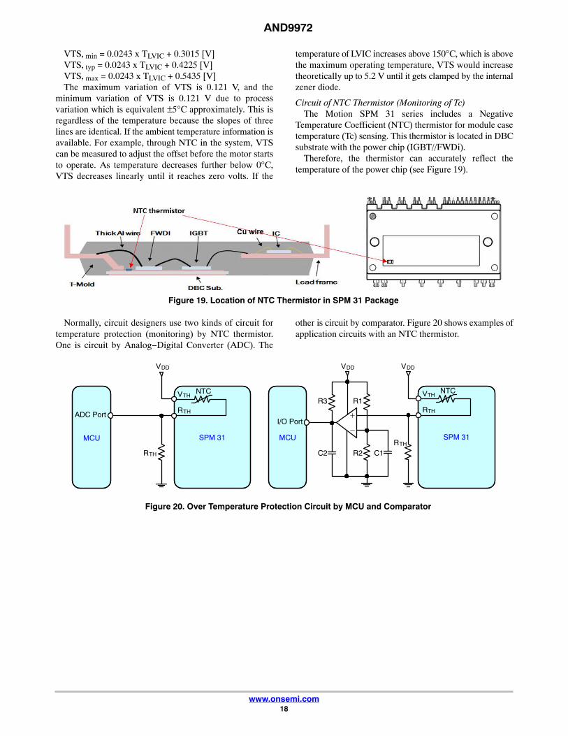
Circuit of NTC Thermistor (Monitoring of Tc)The Motion SPM 31 series includes a Negative
Temperature Coefficient (NTC) thermistor for module casetemperature (Tc) sensing. This thermistor is located in DBCsubstrate with the power chip (IGBT//FWDi).
Therefore, the thermistor can accurately reflect thetemperature of the power chip (see Figure 19).
Figure 19. Location of NTC Thermistor in SPM 31 Package
Normally, circuit designers use two kinds of circuit fortemperature protection (monitoring) by NTC thermistor.One is circuit by Analog−Digital Converter (ADC). The
other is circuit by comparator. Figure 20 shows examples ofapplication circuits with an NTC thermistor.
Figure 20. Over Temperature Protection Circuit by MCU and Comparator
SPM 31MCU
VTH
RTHADC Port
NTC
SPM 31MCU
VTH
RTH
I/O Port
NTC
VDD VDD VDD
RTH
RTH
R2 C1C2
R1R3

AND9972
www.onsemi.com19
Figure 21. V – T Curve of Figure 20
20 30 40 50 60 70 80 90 100 110 1200
1
2
3
4
5
Vctr = 3.3 V
Vctr = 5 V
VOUT(min)
VOUT(typ)
VOUT(max)
V − T Curve at Vctr = 5 V, 3.3 V, RTH = 6.8 k�
Out
put V
olta
ge o
f RT
H [V
]
Temperature TTHERMISTOR [°C]
Table 3. THERMISTOR CHARACTERISTICS (BUILT−IN ONLY IN T TYPE)
Symbol Parameter Condition Min Typ Max Unit
R25 Resistance Tc = 25°C 46.530 47 47.47 k�
R125 Resistance Tc = 125°C 1.344 1.406 1.471 k�
− B−Constant (25 − 50°C) B 4009.5 4050 4090.5 K
− Temperature range − −40 − +125 °C
Figure 22. Thermistor Resistance vs. Temperature
1
10
100
1000
10000
−40 −30 −20 −10 0 10 20 30 40 50 60 70 80 90 100 110 120 130
Thermistor resistance versus Thermistor temperature Tth
min
typ
max
The
rmis
tor
Res
ista
nce
[k�
]
Thermistor Temperature [°C]

AND9972
www.onsemi.com20
Table 4. R−T TABLE OF NTC THERMISTOR
TNTC(�C) Rmin (k�) Rcent (k�) Rmax (k�)
TNTC(�C) Rmin (k�) Rcent (k�) Rmax (k�)
TNTC(�C) Rmin (k�) Rcent (k�) Rmax (k�)
0 154.7426 158.2144 161.748 42 22.257 22.6466 23.0406 84 4.674 2337279 2923493
1 146.9466 150.1651 153.4388 43 21.3574 21.7401 22.1275 85 1210141 1766405 2339470
2 139.5891 142.5725 145.6051 44 20.4988 20.8746 21.2551 86 671043 1214889 4.676
3 132.643 135.4081 138.217 45 19.679 20.0478 20.4216 87 152398 683461 1231325
4 126.0829 128.6453 131.2466 46 18.8961 19.258 19.6249 88 4.0948 171391 706836
5 119.8852 122.2594 124.6681 47 18.1482 18.5032 18.8633 89 3.963 4.1019 201707
6 114.028 116.2273 118.4573 48 17.4337 17.7818 18.135 90 2359893 2855162 4.1118
7 108.4905 110.5275 112.5914 49 16.7508 17.0921 17.4385 91 1912836 2397148 2897165
8 103.2537 105.1398 107.0496 50 16.0981 16.4325 16.7721 92 1482215 1955205 2444265
9 98.2995 100.0454 101.8121 51 15.474 15.8016 16.1346 93 1066935 1529332 2007435
10 93.6111 95.2267 96.8605 52 14.8772 15.1981 15.5243 94 666629 1118799 1585944
11 89.1728 90.6673 92.1776 53 14.3063 14.6205 14.9402 95 280568 722511 1179064
12 84.9699 86.3519 87.7475 54 13.7601 14.0677 14.3808 96 3.1654 341929 788255
13 80.9887 82.2661 83.5552 55 13.2374 13.5385 13.8452 97 3.0675 3.183 411324
14 77.2163 78.3963 79.5865 56 12.737 13.0318 13.332 98 2.973 3.086 47178
15 73.6406 74.7302 75.8283 57 12.258 1302426 2375874 99 2527146 2930373 3.1066
16 70.2503 71.2558 72.2684 58 2225729 12.0815 655217 100 2.794 2600194 3.0137
17 67.0347 67.962 68.8953 59 13455 1629653 2657811 101 1896007 2281338 2680548
18 63.9841 64.8386 65.6981 60 2736307 70068 1076676 102 1596873 1973438 2363882
19 61.0889 61.8759 62.6667 61 1266206 2230811 11.0703 103 1307967 1676132 2058174
20 58.3406 59.0647 59.7918 62 10.1508 800522 1764031 104 1028921 1389050 1762328
21 55.7305 56.3961 57.064 63 9.781 10.0336 371362 105 759372 1111466 1476708
22 53.2515 53.8628 54.4756 64 864044 1765827 2687700 106 498224 842282 1199489
23 50.8962 51.4569 52.0186 65 9.0865 503915 1405333 107 245476 581865 2.445
24 48.6579 49.1715 49.6857 66 2083192 2945164 174831 108 1493 330578 672445
25 46.53 47 47.47 67 940714 1783328 2645665 109 2.1258 87326 421523
26 44.4667 44.936 45.4058 68 8.1472 667512 1510858 110 2.0634 2.1496 179367
27 42.5059 42.9737 43.4423 69 2444021 8.0795 421339 111 2.0034 2.0877 2.1753
28 40.642 41.1075 41.5742 70 1433760 2220492 8.0186 112 2759044 2.0278 2.1135
29 38.8697 39.3323 39.7964 71 461484 1230321 2018513 113 2554144 2848529 2.0538
30 37.184 37.6431 38.104 72 7.0606 278863 1049525 114 2356181 2643992 1.996
31 35.5801 36.0351 36.4923 73 6.815 7.016 118156 115 2164794 2446397 34335
32 34.0537 34.5041 34.9571 74 1421312 2138648 2874977 116 1980347 2255740 2542821
33 32.6007 33.0462 33.4944 75 593307 1294207 2014100 117 1802109 2071657 1.834
34 31.2171 31.6573 32.1005 76 6.1352 484830 1188287 118 1629349 1893054 2168081
35 29.8994 30.3339 30.7717 77 2689403 6.1096 394250 119 1462432 1720659 1989478
36 28.6447 29.0734 29.5055 78 1956362 2610145 6.0887 120 1300631 1553379 1816719
37 27.4492 27.8717 28.2979 79 1251078 1890252 2547324 121 1143576 1390480 1648342
38 26.3098 26.726 27.146 80 572823 1197387 1839484 122 990905 1233061 1485078
39 25.2235 25.6332 26.047 81 5.1688 532646 1160498 123 1.421 1080390 1327293
40 24.1876 24.5907 24.9981 83 2949425 5.1607 506714 124 700902 932467 1173891
41 23.1996 23.596 23.9967 84 2347140 2929702 5.1564 125 1.344 1.406 1025602
AND9972
www.onsemi.com21
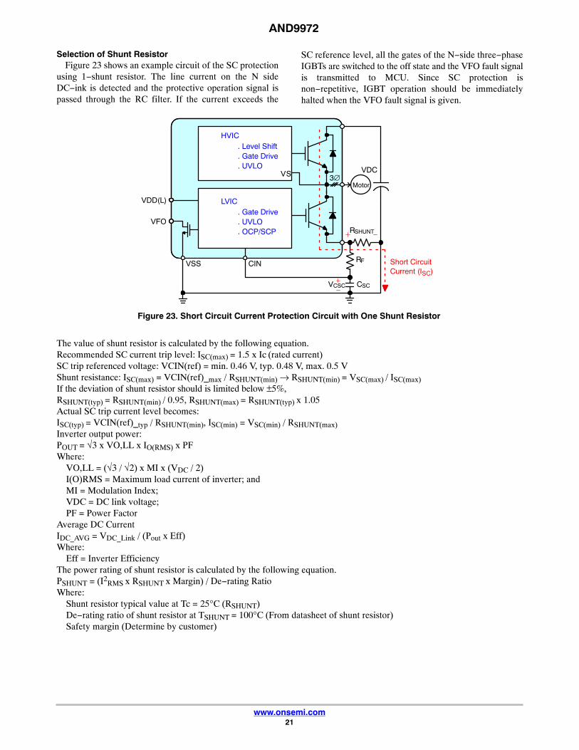
Selection of Shunt ResistorFigure 23 shows an example circuit of the SC protection
using 1−shunt resistor. The line current on the N sideDC−ink is detected and the protective operation signal ispassed through the RC filter. If the current exceeds the
SC reference level, all the gates of the N−side three−phaseIGBTs are switched to the off state and the VFO fault signalis transmitted to MCU. Since SC protection isnon−repetitive, IGBT operation should be immediatelyhalted when the VFO fault signal is given.
Figure 23. Short Circuit Current Protection Circuit with One Shunt Resistor
VS
CIN
HVIC . Level Shift . Gate Drive . UVLO
LVIC . Gate Drive . UVLO . OCP/SCP
VFO
VSS RF
CSC
VDC
VCSC
VDD(L)
Short CircuitCurrent (ISC)
Motor
RSHUNT
3∅
The value of shunt resistor is calculated by the following equation.Recommended SC current trip level: ISC(max) = 1.5 x Ic (rated current)SC trip referenced voltage: VCIN(ref) = min. 0.46 V, typ. 0.48 V, max. 0.5 VShunt resistance: ISC(max) = VCIN(ref)_max / RSHUNT(min) → RSHUNT(min) = VSC(max) / ISC(max)If the deviation of shunt resistor should is limited below ±5%,RSHUNT(typ) = RSHUNT(min) / 0.95, RSHUNT(max) = RSHUNT(typ) x 1.05Actual SC trip current level becomes:ISC(typ) = VCIN(ref)_typ / RSHUNT(min), ISC(min) = VSC(min) / RSHUNT(max)Inverter output power:POUT = √3 x VO,LL x IO(RMS) x PFWhere:
VO,LL = (√3 / √2) x MI x (VDC / 2)I(O)RMS = Maximum load current of inverter; andMI = Modulation Index;VDC = DC link voltage;PF = Power Factor
Average DC CurrentIDC_AVG = VDC_Link / (Pout x Eff)Where:
Eff = Inverter EfficiencyThe power rating of shunt resistor is calculated by the following equation.PSHUNT = (I2
RMS x RSHUNT x Margin) / De−rating RatioWhere:
Shunt resistor typical value at Tc = 25°C (RSHUNT)De−rating ratio of shunt resistor at TSHUNT = 100°C (From datasheet of shunt resistor)Safety margin (Determine by customer)
AND9972
www.onsemi.com22
The value of shunt resistor calculation examples:DUT: NFAM2012L5B(T)Tolerance of shunt resistor: ±5%SC Trip Reference Voltage, VCIN(ref):VCIN(ref)_min = 0.46 V, VCIN(ref)_typ = 0.48 V, VCIN(ref)_max = 0.5 VMaximum Load Current of Inverter (IRMS): 14 ArmsMaximum Peak Load Current of Inverter (IC(max)): 30 AModulation Index (MI): 0.9DC Link Voltage (VDC_Link): 600 VPower Factor (PF): 0.8Inverter Efficiency (Eff): 0.95Shunt Resistor Value at Tc = 25°C (RSHUNT): 16 m�De−rating Ration of Shunt Resistor at TSHUNT = 100°C: 70% (refer to Figure 24)Safety Margin: 20 %
Calculation results:ISC(max): 1.5 x IC(max) = 1.5 x 20 A = 30 ARSHUNT(typ): VCIN(ref)_typ / ISC(max) = 0.48 V / 30 A = 16.0 m�
RSHUNT(max): RSHUNT(max) x 1.05 = 16.0 m� x 1.05A = 16.8 m�
RSHUNT(min): RSHUNT(min) x 0.95 = 16.0 m� x 0.95 A = 15.2 m�
ISC(min): VCIN(ref)_min / RSHUNT(max) = 0.46 V / 16.8 m� = 27.38 AISC(max): VCIN(ref)_max / RSHUNT(min) = 0.5 V / 15.2 m� = 32.89 APOUT = √3 x ((√3 / √2) x MI x (VDC / 2)) x I(O)RMS x PF = (3 / √2) x 0.9 x (600 / 2) x 14 x 0.8 = 6415 WIDC_AVG = (POUT / Eff) / VDC_Link = 11.25 APSHUNT = (I2DC_AVG x RSHUNT x Margin) / De−rating Ratio = (11.252 x 0.016 x 1.2) / 0.7 = 3.47 W (therefore, the proper powerrating of shunt resistor is over 3.5 W).
When over−current events are detected, the 1200 VMotion SPM 31 series shuts down all low−side IGBTs andsends out the fault−out (VFO) signal. FAULT output timeroperation start with internal delay (typ. 2.4 ms, CFOD =22 nF), Fault−out duration time is controlled by CFOD.
To prevent malfunction, it is recommended that an RCfilter be inserted at the CIN pin. To shut down IGBTs within3 �s when over−current situation occurs, a time constant of0.75~1.25 �s is recommended.
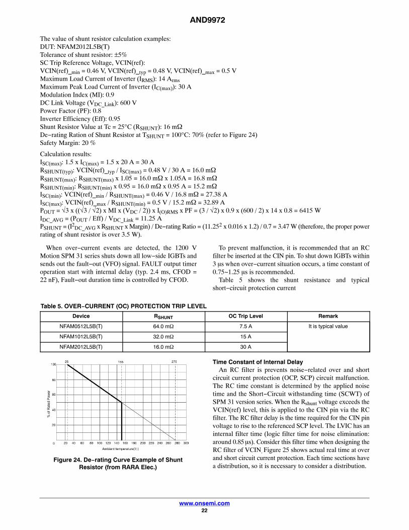
Table 5 shows the shunt resistance and typicalshort−circuit protection current
Table 5. OVER−CURRENT (OC) PROTECTION TRIP LEVEL
Device RSHUNT OC Trip Level Remark
NFAM0512L5B(T) 64.0 m� 7.5 A It is typical value
NFAM1012L5B(T) 32.0 m� 15 A
NFAM2012L5B(T) 16.0 m� 30 A
Figure 24. De−rating Curve Example of ShuntResistor (from RARA Elec.)
Time Constant of Internal DelayAn RC filter is prevents noise−related over and short
circuit current protection (OCP, SCP) circuit malfunction.The RC time constant is determined by the applied noisetime and the Short−Circuit withstanding time (SCWT) ofSPM 31 version series. When the Rshunt voltage exceeds theVCIN(ref) level, this is applied to the CIN pin via the RCfilter. The RC filter delay is the time required for the CIN pinvoltage to rise to the referenced SCP level. The LVIC has aninternal filter time (logic filter time for noise elimination:around 0.85 �s). Consider this filter time when designing theRC filter of VCIN. Figure 25 shows actual real time at overand short circuit current protection. Each time sections havea distribution, so it is necessary to consider a distribution.

AND9972
www.onsemi.com23
Figure 25. Timing Diagram of Over and Short Circuit Protection
Low side IGBTG−E Voltage
FaultOutput Signal
IGBTCurrent
CINVoltage
Detection point
IGBTC−E Voltage
t1
t2
t3
Detection point
t1
t2
t3
Over current condition Short circuit condition
Table 6. TIME TABLE OF OVER AND SHORT CIRCUIT CONDITIONS; VCIN(REF) TO LOW SIDE GATE, COLLECTORCURRENT AND VFO
Ref. Condition VPN = 600 V, VDD = 15 V
Over Current Condition. 2 * I Rating Short Circuit Condition
t1 [�s] t2 [�s] t3 [�s] t1 [�s] t2 [�s] t3 [�s]
Device TJ [�C] Typ Max Typ Max Typ Max Typ Max Typ Max Typ Max
NFAM0512L5B(T) 25 1.05 1.30 TBD TBD 4.0 5.0 1.05 1.30 TBD TBD 4.0 5.0
150 1.0 1.25 TBD TBD 3.2 4.2 1.0 1.25 TBD TBD 3.2 4.2
NFAM1012L5B(T) 25 1.05 1.30 TBD TBD 4.0 5.0 1.05 1.30 TBD TBD 4.0 5.0
150 1.0 1.25 TBD TBD 3.2 4.2 1.0 1.25 TBD TBD 3.2 4.2
NFAM2012L5B(T) 25 1.05 1.30 1.8 2.1 4.0 5.0 1.05 1.30 1.3 1.6 4.0 5.0
150 1.0 1.25 1.75 2.05 3.2 4.2 1.0 1.25 1.1 1.4 3.2 4.2
34.To guarantee safe short−circuit protection under all operating conditions, CIN should be triggered within 1.0 �s after short−circuit occurs.(Recommendation: SCWT < 3.0 �s, Conditions: VDC = 800 V, VDD = 16.5 V, Tj = 150°C).
It is recommended that delay from short−circuit to CINtriggering should be minimized.
NOTES:1. t1: from CIN detection to gate driver LO shut
down2. t2: from CIN detection to collector current 10 %3. t3: from CIN detection to fault out signal
activation
Fault Output CircuitBecause VFO terminal is an open−drain type, it should be
pulled up via a pull−up resistor.
Vctr
/Fo
ADCR1
VFO
SPM 31
MCU
Figure 26. Voltage−Current Characteristics of VFOTerminal

AND9972
www.onsemi.com24
0.0 0.2 0.4 0.6 0.8 1.0 1.2 1.4 1.6 1.8 2.00.00
0.05
0.10
0.15
0.20
0.25
0.30
0.35
0.40
Figure 27. Voltage−Current Characteristics of VFOTerminal
TJ = 150°C
IFO [mA]
VF
O [m
V]
Circuit of Input Signal (HINx, LINx)Figure 28 shows recommended I/O interface circuit
between the MCU and SPM 31. Because SPM 31 input logicis active HIGH and there are built−in pull−down resistors,external pull−down resistors are not needed.
Since the fault output is open drain and its rating isVDD + 0.3 V, 15 V supply interface is possible.
However, it is recommended that the fault output beconfigured with the 5 V logic supplies, which is the same asthe input signals. It is also recommended that the decouplingcapacitors be placed at both the MCU and Motion SPM 31ends of the VFO signal line, as close as possible to eachdevice. The RC coupling at each input (parts shown dottedin Figure 28) can be changed depending on the PWM controlscheme used in the application and the wiring impedance ofthe PCB layout.
The input signal section of the Motion SPM 31 seriesintegrates a 5 k� (typical) pull−down resistor. Therefore,when using an external filtering resistor between the MCUoutput and the Motion SPM 31 input, attention should begiven to the signal voltage drop at the Motion SPM 31 inputterminals to satisfy the turn−on threshold voltagerequirement. For instance, R = 100 � and C = 1 nF for theparts shown dotted in Figure 28.
Figure 28. Recommended MCU I/O Interface Circuit
5 V−Line
HIN(X)
LIN(X)
VFO
VSS
C = 1 nF
SPM 31MCU
GateDriver
Level−ShiftCircuit
Typ. 5 k�
InputNoiseFilter
InputNoiseFilter
GateDriver
Typ. 5 k�
HIN(X) tIN(FLT) = Typ. 500 ns for turn onTyp. 400 Ns for turn off
LIN(X) tIN(FLT) = Typ. 650 ns for turn onTyp. 750 ns for turn off
R = 10 k�
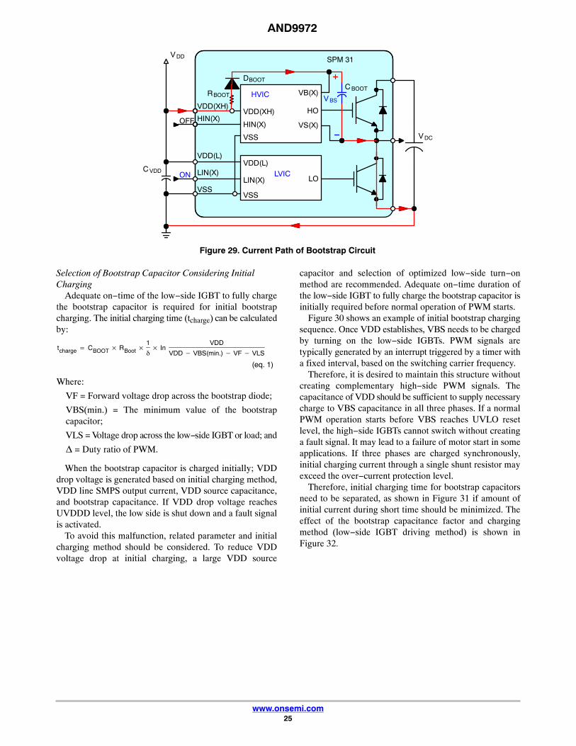
Bootstrap Circuit DesignOperation of Bootstrap Circuit
The VBS voltage, which is the voltage difference betweenVB(U,V,W) and VS(U,V,W), provides the supply to theHVIC within the 1200 V SPM 31 series. This supply mustbe in the range of 13.0 V~18.5 V to ensure that the HVIC canfully drive the high−side IGBT. The SPM 31 series includesan under−voltage lock out protection function for the VBSto ensure that the HVIC does not drive the high−side IGBT,if the VBS voltage drops below a specified voltage. Thisfunction prevents the IGBT from operating in a high
dissipation mode. There are a number of ways in which theVBS floating supply can be generated. One of them is thebootstrap method described here (refer to Figure 29). Thismethod has the advantage of being simples and inexpensive.However, the duty cycle and on−time are limited by therequirement to refresh the charge in the bootstrap capacitor.The bootstrap to ground (either through the low−side or theload), the bootstrap capacitor (CBOOT) is charged throughthe bootstrap diode (DBOOT) and the resistor (RBOOT) fromthe VDD supply
AND9972
www.onsemi.com25
Figure 29. Current Path of Bootstrap Circuit
VS(X)
HVIC
LVIC
V DC
VDD(L)
VB(X)
VDD(XH)VDD(XH)
LIN(X)
C BOOT
C VDD
SPM 31
DBOOT
VSS
VDD(L)
VSS
HO
LOVSS
V DD
V BS
HIN(X)HIN(X)
LIN(X)
OFF
ON
RBOOT
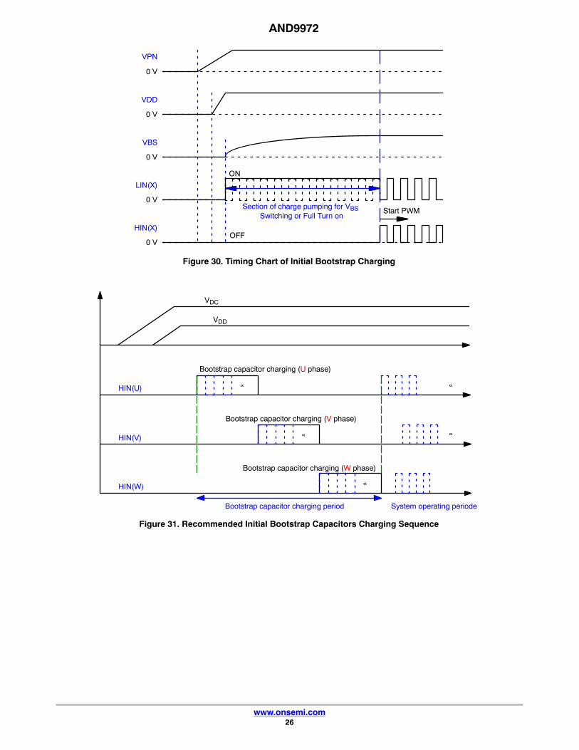
Selection of Bootstrap Capacitor Considering InitialCharging
Adequate on−time of the low−side IGBT to fully chargethe bootstrap capacitor is required for initial bootstrapcharging. The initial charging time (tcharge) can be calculatedby:
tcharge � CBOOT � RBoot �1
�� In
VDD
VDD � VBS(min.) � VF � VLS
(eq. 1)
Where:
VF = Forward voltage drop across the bootstrap diode;
VBS(min.) = The minimum value of the bootstrapcapacitor;
VLS = Voltage drop across the low−side IGBT or load; and
�� = Duty ratio of PWM.
When the bootstrap capacitor is charged initially; VDDdrop voltage is generated based on initial charging method,VDD line SMPS output current, VDD source capacitance,and bootstrap capacitance. If VDD drop voltage reachesUVDDD level, the low side is shut down and a fault signalis activated.
To avoid this malfunction, related parameter and initialcharging method should be considered. To reduce VDDvoltage drop at initial charging, a large VDD source
capacitor and selection of optimized low−side turn−onmethod are recommended. Adequate on−time duration ofthe low−side IGBT to fully charge the bootstrap capacitor isinitially required before normal operation of PWM starts.
Figure 30 shows an example of initial bootstrap chargingsequence. Once VDD establishes, VBS needs to be chargedby turning on the low−side IGBTs. PWM signals aretypically generated by an interrupt triggered by a timer witha fixed interval, based on the switching carrier frequency.
Therefore, it is desired to maintain this structure withoutcreating complementary high−side PWM signals. Thecapacitance of VDD should be sufficient to supply necessarycharge to VBS capacitance in all three phases. If a normalPWM operation starts before VBS reaches UVLO resetlevel, the high−side IGBTs cannot switch without creatinga fault signal. It may lead to a failure of motor start in someapplications. If three phases are charged synchronously,initial charging current through a single shunt resistor mayexceed the over−current protection level.
Therefore, initial charging time for bootstrap capacitorsneed to be separated, as shown in Figure 31 if amount ofinitial current during short time should be minimized. Theeffect of the bootstrap capacitance factor and chargingmethod (low−side IGBT driving method) is shown inFigure 32.
AND9972
www.onsemi.com26
Figure 30. Timing Chart of Initial Bootstrap Charging
VPN
VDD
VBS
LIN(X)
ON
Start PWM
HIN(X)OFF
0 V
0 V
0 V
0 V
0 V
Section of charge pumping for VBS Switching or Full Turn on
Figure 31. Recommended Initial Bootstrap Capacitors Charging Sequence
«
«
«
«
«
VDC
VDD
Bootstrap capacitor charging (U phase)
HIN(U)
HIN(V)
HIN(W)
Bootstrap capacitor charging (V phase)
Bootstrap capacitor charging (W phase)
Bootstrap capacitor charging period System operating periode

AND9972
www.onsemi.com27
Figure 32. Initial Charging According to Bootstrap Capacitance and Charging Method (Ref. Condition: VDD = 15 V / 300 mA, VDD Capacitor = 220 �F, CBOOT = 100 �F, RBOOT = 20 �)
LIN(U, V, W) [5 V/div.]
VFO [5 V/div.]
VDD [5 V/div.]
VBS [5 V/div.]
All low side turns on at a same time
Time [2 ms/div.]
VFO is activated by UVDDLIN(X) [5 V/div.]
Only one low side turns on
LIN(U, V, W) [5 V/div.]
CBOOT = 16 �F
CBOOT = 50 �F
All low side turns on at a same time
LIN(U, V, W) [5 V/div.]
VFO [5 V/div.]
VDD [5 V/div.]
VBS [5 V/div.]
Time [2 ms/div.]
LIN(U, V, W) [5 V/div.]
VFO is activated by UVDD
CBOOT = 50 �F
All low side turns on withFSW = 5 kHz, Duty = 50%
LIN(U, V, W) [5 V/div.]VFO is activated by UVDD
CBOOT = 50 �F
All low side turns on at a same time
CBOOT = 50 �F
CBOOT = 50 �F
All low side turns on withFSW = 5 kHz, Duty = 25%
Selection of Bootstrap Capacitor Considering OperatingThe bootstrap capacitance can be calculated by:
CBOOT �
Ileak � �t
�VBS (eq. 2)
Where:
�t: maximum on pulse width of high−side IGBT;
�VBS: the allowable discharge voltage of the CBOOT(voltage ripple); and
ILeak: maximum discharge current of the CBOOT.
Mainly via the following mechanisms:
Gate charge for turning the high−side IGBT on.
Quiescent current to the high−side circuit in HVIC.
Level−shift charge required by level−shifters in HVIC.
Leakage current in the bootstrap circuit.
CBOOT capacitor leakage current (ignored fornon−electrolytic capacitors).
Bootstrap diode reverse recovery charge.
Practically, 4.5 mA of I Leak is recommended for the1200 V SPM 31 series. By considering dispersion andreliability, the capacitance is generally selected to be2~3 times the calculated one. The CBOOT is only chargedwhen the high−side IGBT is off and the VS(x) voltage ispulled down to ground.
The on−time of the low−side IGBT must be sufficient tofor the charge drawn from the CBOOT capacitor to be fullyreplenished. This creates an inherent minimum on−time ofthe low−side IGBT (or off−time of the high−side IGBT).

AND9972
www.onsemi.com28
Figure 33. Capacitance of Bootstrap Capacitor on Variation of Switching Frequency
0 2 4 6 8 10 12 14 16 18 200
10
20
30
40
50
60
70
80
90
100
110
6.8 [�F]
Continuous Sinusoidal Current Control
10 [�F]
22 [�F]
33 [�F]
47 [�F]
100 [�F]
Conditions: �VBS = 0.1 [V], ILEAK = 4.5 [mA]
Minimum Value Recommend Value Commercial Capacitance
Boo
tstr
ap C
apac
itanc
e, C
BS [�
F]
Switching Frequency, FSW [kHz]
CBS_min = (ILEAK x �t) / �VBS
Based on switching frequency and recommended �VBS.
ILeak: circuit current = 4.5 mA (recommended value)
��VBS: discharged voltage = 1.0 V (recommended value)
��t: maximum on pulse width of high−side IGBT = 0.2 ms(depends on application)CBOOT_min = ((Ileak x �t) / �VBS) = ((4.5 mA x 0.2 ms) /1.0 V) = 9 x 10⁻⁶
→ More than 2 times → 18 �F. (22 �F STD value)
NOTE: The capacitance value can be changed accordingto the switching frequency, the capacitorselected, and the recommended VBS voltage of13.0~18.5 V (from datasheet). The above resultis just a calculation example. This value can bechanged according to the actual control methodand lifetime of the component.
Built−in Bootstrap CircuitWhen the low−side IGBT or diode conducts, the bootstrap
diode (DBOOT) supports the entire bus voltage. Hence, adiode with withstand voltage of more than 1200 V isrecommended. It is important that this diode has a fast
recovery (recovery time <100 ns) characteristic to minimizethe amount of charge fed back from the bootstrap capacitorinto the VDD supply. The bootstrap resistor (RBOOT) is toslow down the dVBS/dt and limit initial charging current(Icharge) of bootstrap capacitor.
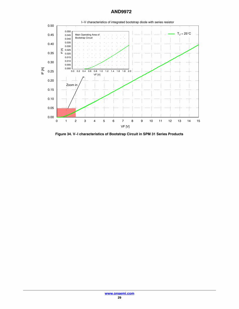
Normally, a bootstrap circuit consists of bootstrap diode(DBOOT), bootstrap resistor (RBOOT), and bootstrapcapacitor (CBOOT). As shown in Figure 34, the built−inbootstrap circuit of SPM 31 product has series resistor to beused without additional bootstrap resistor. Therefore, onlyexternal bootstrap capacitors are needed to make bootstrapcircuit.
The characteristics of the built−in bootstrap diode in theSPM 31 products are:
Fast recovery diode: more than 1200 V / 2 AResistive characteristic: equivalent resistor ofapproximately 38 �Table 7 shows the specification of bootstrap circuit.
Figure 34 shows forward voltage drop and reverse recoverycharacteristic of the bootstrap diode.
Table 7. SPECIFICATION FOR INTEGRATED BOOTSTRAP CIRCUIT
Symbol Parameter Conditions Min Typ Max Unit
VF Forward−Drop Voltage If = 0.1 A, Tc = 25°C 3.4 4.6 5.8 V
RBOOT Built−in Limiting Resistance 30 38 46 �
AND9972
www.onsemi.com29
0 1 2 3 4 5 6 7 8 9 10 11 12 13 14 150.00
0.05
0.10
0.15
0.20
0.25
0.30
0.35
0.40
0.45
0.50I−V characteristics of integrated bootstrap diode with series resistor
IF [A
]
VF [V]
TJ = 25°C
Zoom in
Figure 34. V−I characteristics of Bootstrap Circuit in SPM 31 Series Products
0.0 0.2 0.4 0.6 0.8 1.0 1.2 1.4 1.6 1.8 2.00.000
0.005
0.010
0.015
0.020
0.025
0.030
0.035
0.040
0.045
0.050
IF [A
]
VF [V]
Main Operating Area ofBootstrap Circuit

AND9972
www.onsemi.com30
PRINT CIRCUIT BOARD (PCB) DESIGN
General Application Circuit ExampleFigure 35 shows a general application circuitry of
interface schematic with control signals connected directlyto a MCU. Figure 36 shows guidance of PCB layout for the1200 V SPM 31 series.
Figure 35. General Application Circuitry for 1200 V Motion SPM 31
HIN(U) (6)
HVIC1VDD(UH) (4)
VB(U) (3)
VS(U) (1)
LIN(V) (22)
VTS (20)
LIN(U) (21)
VTH (38)
U (36)
P (37)
V (35)
W (34)
NU (33)
NV (32)
NW (31)
RTH (39)
NTC Thermistor
VS
HIN
VDD
VB
VSS
HOUT
HIN(V) (12)
HVIC2VDD(VH) (10)
VB(V) (9)
VS(V) (7)
VS
VB
VSS
HOUT
HIN(W) (18)
HVIC3VDD(WH) (16)
VB(W) (15)
VS(W) (13)
VS
VB
VSS
HOUT
LVIC
OUT(U)
OUT(V)
OUT(W)
LIN(W) (23)
VFO (24)
CFOD (25)
CIN (26)
VSS (27)
VDD(L) (28)
VTS
LIN(U)
LIN(V)
LIN(W)
VFO
CFOD
CIN
VSS
VDD
+ C1
Phase current
Motor
CS
MCU
Signal for over current protection
HIN
VDD
HIN
VDD
5V line
15V line
5 V line
AND9972
www.onsemi.com31
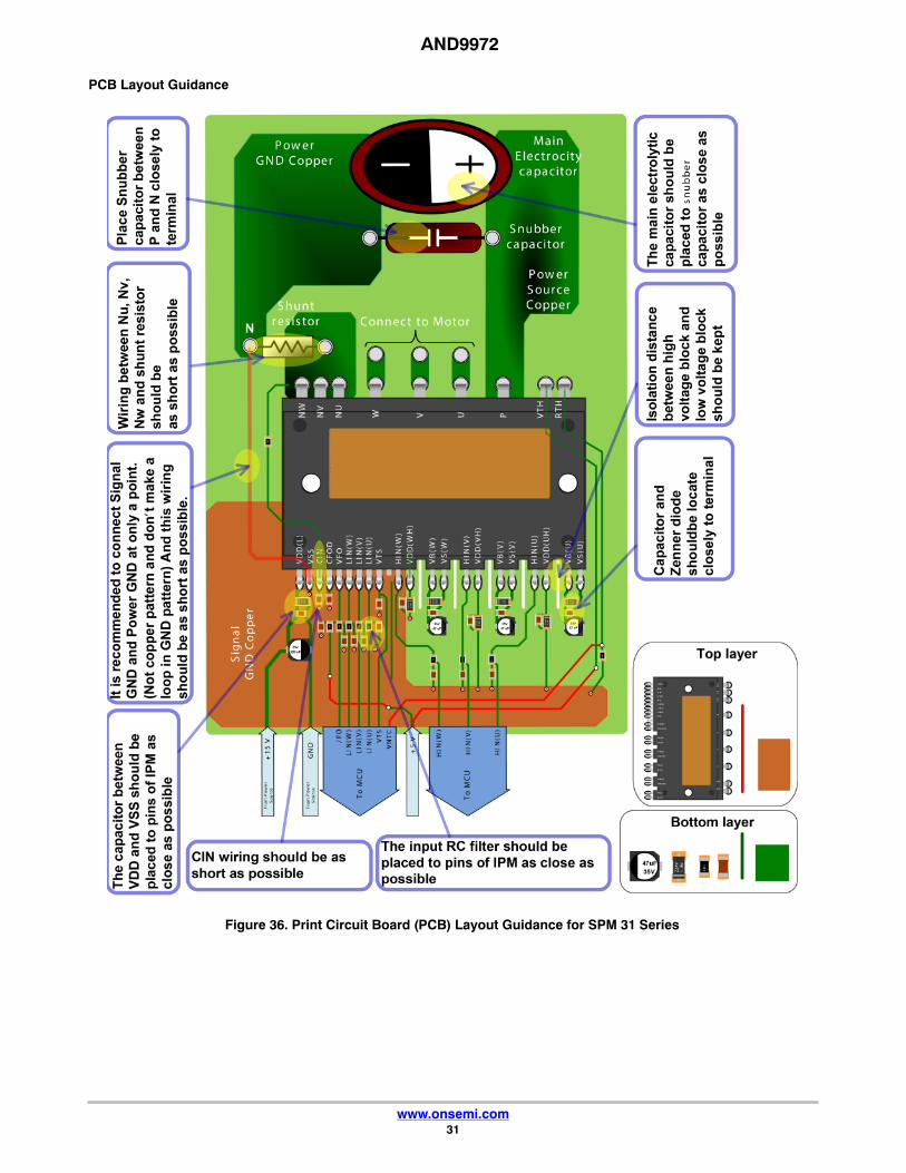
PCB Layout Guidance
Figure 36. Print Circuit Board (PCB) Layout Guidance for SPM 31 Series

AND9972
www.onsemi.com32
ON Semiconductor and are trademarks of Semiconductor Components Industries, LLC dba ON Semiconductor or its subsidiaries in the United States and/or other countries.ON Semiconductor owns the rights to a number of patents, trademarks, copyrights, trade secrets, and other intellectual property. A listing of ON Semiconductor’s product/patentcoverage may be accessed at www.onsemi.com/site/pdf/Patent−Marking.pdf. ON Semiconductor reserves the right to make changes without further notice to any products herein.ON Semiconductor makes no warranty, representation or guarantee regarding the suitability of its products for any particular purpose, nor does ON Semiconductor assume any liabilityarising out of the application or use of any product or circuit, and specifically disclaims any and all liability, including without limitation special, consequential or incidental damages.Buyer is responsible for its products and applications using ON Semiconductor products, including compliance with all laws, regulations and safety requirements or standards,regardless of any support or applications information provided by ON Semiconductor. “Typical” parameters which may be provided in ON Semiconductor data sheets and/orspecifications can and do vary in different applications and actual performance may vary over time. All operating parameters, including “Typicals” must be validated for each customerapplication by customer’s technical experts. ON Semiconductor does not convey any license under its patent rights nor the rights of others. ON Semiconductor products are notdesigned, intended, or authorized for use as a critical component in life support systems or any FDA Class 3 medical devices or medical devices with a same or similar classificationin a foreign jurisdiction or any devices intended for implantation in the human body. Should Buyer purchase or use ON Semiconductor products for any such unintended or unauthorizedapplication, Buyer shall indemnify and hold ON Semiconductor and its officers, employees, subsidiaries, affiliates, and distributors harmless against all claims, costs, damages, andexpenses, and reasonable attorney fees arising out of, directly or indirectly, any claim of personal injury or death associated with such unintended or unauthorized use, even if suchclaim alleges that ON Semiconductor was negligent regarding the design or manufacture of the part. ON Semiconductor is an Equal Opportunity/Affirmative Action Employer. Thisliterature is subject to all applicable copyright laws and is not for resale in any manner.
PUBLICATION ORDERING INFORMATIONTECHNICAL SUPPORTNorth American Technical Support:Voice Mail: 1 800−282−9855 Toll Free USA/CanadaPhone: 011 421 33 790 2910
SPM is registered trademark of Semiconductor Components Industries, LLC (SCILLC) or its subsidiaries in the United States and/or other countries.
LITERATURE FULFILLMENT:Email Requests to: [email protected]
ON Semiconductor Website: www.onsemi.com
Europe, Middle East and Africa Technical Support:Phone: 00421 33 790 2910For additional information, please contact your local Sales Representative
◊