Analytical solutions of ac electrokinetics in ... · taken to be the gradient of a scalar...
18
Analytical solutions of ac electrokinetics in interdigitated electrode arrays: Electric field, dielectrophoretic and traveling-wave dielectrophoretic forces Tao Sun, * Hywel Morgan, and Nicolas G. Green † Nanoscale Systems Integration Group, School of Electronics and Computer Science, University of Southampton, SO17 1BJ United Kingdom Received 5 June 2007; revised manuscript received 21 August 2007; published 25 October 2007 Analysis of the movement of particles in a nonuniform field requires accurate knowledge of the electric field distribution in the system. This paper describes a method for analytically solving the electric field distribution above interdigitated electrode arrays used for dielectrophoresis DEP and traveling wave dielectrophoresis twDEP, using the Schwarz-Christoffel mapping method. The electric field solutions are used to calculate the dielectrophoretic force in both cases, and the traveling wave dielectrophoretic force and the electrorotational torque for the twDEP case. This method requires no approximations and can take into account the Neumann boundary condition used to represent an insulating lid and lower substrate. The analytical results of the electric field distributions are validated for different geometries by comparison with numerical simulations using the finite element method. DOI: 10.1103/PhysRevE.76.046610 PACS numbers: 41.20.q I. INTRODUCTION In the field of micro total analysis systems TAS or the lab-on-a-chip LOC, the manipulation, separation, and char- acterization of biological particles can be performed using electrical techniques based on ac electrokinetics 1. When an electric field is applied to a suspension of particles, charges accumulate at the interface between the particle and the fluid medium, a phenomenon known as Maxwell-Wagner interfacial polarization. This produces an induced dipole mo- ment across the particle, the magnitude and direction de- pending on the difference in the polarizability of the particle and the medium. The interaction between the induced dipole moment and a nonuniform electric field produces an unbal- anced force on the two poles, which results in the transla- tional movement of the particles. Applications in this area include manipulating, separating, trapping and sorting par- ticles such as cells, bacteria, and viruses 2–8, using dielec- trophoresis DEP9,10, electrorotation ROT11,12, and traveling wave dielectrophoresis twDEP13–15. DEP is the movement of the particles in the nonuniform electric field, due to the imbalance of force on the two sides poles of the particle. This movement is towards regions of high or low field strength depending on whether the particle is more or less polarizable than the medium at the applied frequency. The DEP force depends on the in-phase compo- nent of the effective dipole 16,17. ROT occurs when the field has a nonuniform phase, which means that there is a rotational component to the field. The direction of the effec- tive dipole lags behind the turning field vector, leading to torque on the particle which depends on the out-of-phase component of the dipole 18,19. For further details on the relationship between DEP and ROT see Wang et al. 20,21. In electric fields with spatially varying phases, a particle ex- periences a linear force in addition to the DEP force which depends on the out-of-phase component of the effective di- pole. This is referred to as traveling wave dielectrophoresis twDEP, since it was first observed in traveling electric fields 22. This method can be used to separate or fraction- ate particles without the need to pump a liquid through the device. A number of microfluidic devices with different micro- channel geometries and microelectrode patterns have been used for DEP and twDEP. Since the interaction between the electric field and the induced dipole is the origin of the mo- tion of the particles, it is important to characterize the strength and direction of the electric field in the system. Un- fortunately, accurate analytical electric field solutions are generally difficult to obtain due to the complicated structures of the microelectrodes and the geometries of the microde- vices. Even for the most commonly used interdigitated elec- trode arrays, no strict and computationally efficient analyti- cal solution has been reported. Previous analytical solutions use Green’s theorem 23, Green’s function 24,25, half- plane Green’s function 26 and Fourier series 27,28. How- ever, these analytical solutions all involve approximations. In both the Green’s theorem and Fourier series methods, it is assumed that the potential varies linearly with distance in the electrode gaps. In the method of Green’s function, the gradi- ent of the electric field magnitude squared is influenced by the choice of a characteristic length scale. In the method of half-plane Green’s function, a linear approximation for the surface potential in the gaps between the electrodes is adopted. Other approaches, such as the charge density method 29 and numerical simulation 30 are accurate but computationally expensive. In this paper, we present analytical solutions of the elec- tric field distribution above interdigitated electrode arrays in both DEP and twDEP applications using the Schwarz- Christoffel mapping SCM method. This method requires no approximations and the results are straightforward to use. In other analytical solutions 23–27, the presence of the upper *[email protected] † [email protected] PHYSICAL REVIEW E 76, 046610 2007 1539-3755/2007/764/04661018 ©2007 The American Physical Society 046610-1
Transcript of Analytical solutions of ac electrokinetics in ... · taken to be the gradient of a scalar...
Analytical solutions of ac electrokinetics in interdigitated electrode arrays: Electric field,dielectrophoretic and traveling-wave dielectrophoretic forces
Tao Sun,* Hywel Morgan, and Nicolas G. Green†
Nanoscale Systems Integration Group, School of Electronics and Computer Science, University of Southampton,SO17 1BJ United Kingdom
�Received 5 June 2007; revised manuscript received 21 August 2007; published 25 October 2007�
Analysis of the movement of particles in a nonuniform field requires accurate knowledge of the electric fielddistribution in the system. This paper describes a method for analytically solving the electric field distributionabove interdigitated electrode arrays used for dielectrophoresis �DEP� and traveling wave dielectrophoresis�twDEP�, using the Schwarz-Christoffel mapping method. The electric field solutions are used to calculate thedielectrophoretic force in both cases, and the traveling wave dielectrophoretic force and the electrorotationaltorque for the twDEP case. This method requires no approximations and can take into account the Neumannboundary condition used to represent an insulating lid and lower substrate. The analytical results of the electricfield distributions are validated for different geometries by comparison with numerical simulations using thefinite element method.
DOI: 10.1103/PhysRevE.76.046610 PACS number�s�: 41.20.�q
I. INTRODUCTION
In the field of micro total analysis systems ��TAS� or thelab-on-a-chip �LOC�, the manipulation, separation, and char-acterization of biological particles can be performed usingelectrical techniques based on ac electrokinetics �1�. Whenan electric field is applied to a suspension of particles,charges accumulate at the interface between the particle andthe fluid medium, a phenomenon known as Maxwell-Wagnerinterfacial polarization. This produces an induced dipole mo-ment across the particle, the magnitude and direction de-pending on the difference in the polarizability of the particleand the medium. The interaction between the induced dipolemoment and a nonuniform electric field produces an unbal-anced force on the two poles, which results in the transla-tional movement of the particles. Applications in this areainclude manipulating, separating, trapping and sorting par-ticles such as cells, bacteria, and viruses �2–8�, using dielec-trophoresis �DEP� �9,10�, electrorotation �ROT� �11,12�, andtraveling wave dielectrophoresis �twDEP� �13–15�.
DEP is the movement of the particles in the nonuniformelectric field, due to the imbalance of force on the two sides�poles� of the particle. This movement is towards regions ofhigh or low field strength depending on whether the particleis more or less polarizable than the medium at the appliedfrequency. The DEP force depends on the in-phase compo-nent of the effective dipole �16,17�. ROT occurs when thefield has a nonuniform phase, which means that there is arotational component to the field. The direction of the effec-tive dipole lags behind the turning field vector, leading totorque on the particle which depends on the out-of-phasecomponent of the dipole �18,19�. For further details on therelationship between DEP and ROT see Wang et al. �20,21�.In electric fields with spatially varying phases, a particle ex-
periences a linear force in addition to the DEP force whichdepends on the out-of-phase component of the effective di-pole. This is referred to as traveling wave dielectrophoresis�twDEP�, since it was first observed in traveling electricfields �22�. This method can be used to separate or fraction-ate particles without the need to pump a liquid through thedevice.
A number of microfluidic devices with different micro-channel geometries and microelectrode patterns have beenused for DEP and twDEP. Since the interaction between theelectric field and the induced dipole is the origin of the mo-tion of the particles, it is important to characterize thestrength and direction of the electric field in the system. Un-fortunately, accurate analytical electric field solutions aregenerally difficult to obtain due to the complicated structuresof the microelectrodes and the geometries of the microde-vices. Even for the most commonly used interdigitated elec-trode arrays, no strict and computationally efficient analyti-cal solution has been reported. Previous analytical solutionsuse Green’s theorem �23�, Green’s function �24,25�, half-plane Green’s function �26� and Fourier series �27,28�. How-ever, these analytical solutions all involve approximations. Inboth the Green’s theorem and Fourier series methods, it isassumed that the potential varies linearly with distance in theelectrode gaps. In the method of Green’s function, the gradi-ent of the electric field magnitude squared is influenced bythe choice of a characteristic length scale. In the method ofhalf-plane Green’s function, a linear approximation for thesurface potential in the gaps between the electrodes isadopted. Other approaches, such as the charge densitymethod �29� and numerical simulation �30� are accurate butcomputationally expensive.
In this paper, we present analytical solutions of the elec-tric field distribution above interdigitated electrode arrays inboth DEP and twDEP applications using the Schwarz-Christoffel mapping �SCM� method. This method requires noapproximations and the results are straightforward to use. Inother analytical solutions �23–27�, the presence of the upper
*[email protected]†[email protected]
PHYSICAL REVIEW E 76, 046610 �2007�
1539-3755/2007/76�4�/046610�18� ©2007 The American Physical Society046610-1
surface of the fluidic channel �the insulating lid in real de-vices� imposes a Neumann condition on the solution of thepotential, a factor that was not considered. In Ref. �28�, thiscondition was analyzed using a closed form of Fourier series,but the solution approximates the potential distribution in theelectrode gaps to a linear function.
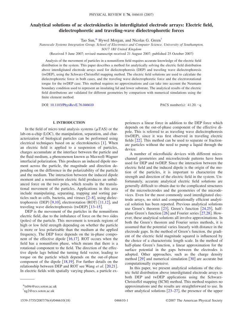
When interdigitated electrode arrays are used for the ap-plication of DEP, two ac voltage signals of angular frequency� with phases 0° and 180° are alternately connected to theelectrodes to generate a nonuniform electric field with a spa-tially constant phase. For twDEP, four signals with phaseshifts of 90° are sequentially applied to the electrodes in thearray, generating a traveling electric field with a spatiallydependent phase. Figure 1 shows a schematic of the systemand the geometrical parameters for the electrodes and thechannel with the different potentials for DEP and twDEP,respectively.
In Sec. II, we briefly review fundamental ac electrokinetictheory and the principle of SCM method with the commonboundary conditions used in the electric field analysis ofDEP and twDEP electrode arrays. Due to the different ap-plied potentials in DEP and twDEP electrode arrays, the ge-ometries of the problem spaces are different and the solu-tions for the two cases are discussed in Secs. III and IVseparately. Analytical electric field solutions are derived inboth cases and validated by numerical simulations using thefinite element method �FEM�. The field solutions are used tocalculate the DEP force in the DEP and twDEP arrays andtwDEP force and ROT torque in the twDEP array.
II. THEORY
For DEP and twDEP experiments and calculations, thegeneral approach is to assume that the field is quasi-electrostatic �1,24,27,30�. This assumes that the electric fieldis irrotational �an implicit assumption in the derivation of theDEP and twDEP forces�, or that the currents in the systemare slow time-varying. As a result, the electric field can betaken to be the gradient of a scalar potential.
A. Fields and DEP force in interdigitated electrode arrays
For an ac potential of single frequency, the electric fieldcan be expressed using complex phasor notation �1,11,14� as
E=Re�Eej�t�, where j2=−1, � is the angular frequency ofthe electric field, t is time, Re �¯� indicates the real part of
�¯� and E=−��=−���R+ j��I� is the general complex
amplitude of the electric field. �=�R+ j�I is the complexelectrical potential phasor with �R and �I as the real andimaginary components respectively.
The time-averaged dielectrophoretic force on the dipole is�1�
�F� =1
2Re��p · ��E*� =
1
2v Re���E · ��E*� , �1�
where p is the induced dipole moment phasor, v the volumeof the particle, � the effective polarizability, and � indicatescomplex conjugate.
Equation �1� can be rewritten as
�F� =1
4v Re��� � �E�2 −
1
2v Im���„� � �Re�E� � Im�E��… ,
�2�
where �E�2= �Re�E��2+ �Im�E��2 and Im�¯� indicates theimaginary part of �¯�.
Equation �2� shows that the dielectrophoretic force con-sists of two components; the first term on the right is theconventional DEP force; the second term the twDEP force.Conventional DEP occurs in a nonuniform electric field. Inorder to calculate the DEP force, we need to know the vol-ume and polarizability of the particle and the field-related
component, ��E�2, which we term the “dielectrophoreticforce component” in this paper, and obtained from fieldanalysis. The twDEP force occurs whenever the imaginary�out-of-phase� part of the effective polarizability is nonzeroand giving a spatial phase variation. As particles move in thex-y 2D plane �Fig. 1�, they will simultaneously experience anelectrorotational torque in the third direction �z axis�. ThisROT torque is given by
��� =1
2Re�p � E*� = − v Im����Re�E� � Im�E�� . �3�
Similarly, the field-related components �� �Re�E�� Im�E�� and Re�E�� Im�E� are termed the “traveling wavedielectrophoretic force component” and the “electrorota-tional torque component,” respectively, and are obtainedfrom the analytical electric field solution.
B. Schwarz-Christoffel mapping (SCM) method
The SCM method maps the upper half of a complex plane�T-plane� into the interior of a given polygon in another com-plex plane �Z-plane�. The Z-plane represents the real systemin our case. Complex numbers in this plane represent vectorsin the real system, with the real component representing thehorizontal direction �x-axis� and the imaginary componentthe vertical direction �y-axis�. A general mathematical de-
Glass Lid
GlassSubstrate
ElectrolyteElectrodes
Phases of the appliedpotential signals for DEP
w gh
0o
0o 180o
180o
0o
180o
0o 90o
270o
0oPhases of the appliedpotential signals for twDEP
x
yz
FIG. 1. Diagram showing the experimental system, consisting ofthe interdigitated electrode array used for dielectrophoresis �DEP�and traveling wave dielectrophoresis �twDEP�. For DEP, the elec-trodes are connected to voltages with 180° phase shifts. For twDEP,the electrodes are connected to a frequency generator with 90°phase shift. w is the electrode width, g is the electrode gap, and h isthe height of the channel.
SUN, MORGAN, AND GREEN PHYSICAL REVIEW E 76, 046610 �2007�
046610-2
scription of the SCM method is provided in Appendix A, andfurther details can be found in �31�.
For the electric field analysis, a nonuniform two-dimensional electric field polygonal region is transformedinto an equivalent rectangular region �a parallel plate capaci-tor�, where the electric field distribution is uniform, as fol-lows.
�a� Select a basic cell for the physical two-dimensionalgeometry using symmetrical axes in the physical plane�Z-plane�. Determine the boundary conditions �i.e., Neumannor Dirichlet condition� along each boundary of the cell.
�b� Apply SCM method to map the basic cell from theZ-plane to the upper half of the auxiliary plane �T-plane�.
�c� Apply a second SCM method to transform the upperhalf of the T-plane into a closed parallel plate capacitor re-gion in the model plane �W-plane�.
The original nonuniform field problem in the Z-plane canthen be easily solved in the W-plane. The details of the trans-formation procedure along with the analysis of the electricfield are described in the following sections.
The SCM method has been used to solve problems inelectrostatics and magnetostatics �32,33�, transmission linesand waveguides �34–37�, temperature distribution and heattransfer �38,39� and fluid flow �40�. Latterly, conformal map-ping has been used to analyze electromagnetic field problemsin MEMS devices, including coupling capacitance in comb-finger actuators �41� and forces in electromechanical actua-tors �42�. Gevorgian’s group �43–46� has used conformalmapping to model interdigital capacitors �IDC� or coplanar-strip waveguides �CPW�, which have similar geometry to theinterdigitated electrode arrays. In particular, in Ref. �43�, theperiodical structure of a single-layer substrate IDC has thesame geometry and boundary conditions as the DEP elec-trode array. However the authors used a metal strip assump-tion to simplify the problem by changing the closed geom-etry to a semi-infinite channel, in order to avoid the complexexpressions in the transformations for the original geometry,which involve both Jacobian elliptic functions and ellipticintegrals. In this paper, we solve the problem of the DEPelectrode array without altering the geometry. The derivedexpressions of the elliptic integrals can be also applied tocalculate the capacitances of the IDC in �43� as a completesolution, but this work is beyond the scope of this paper. Weare interested in utilizing the analytical electric field solutionto characterize the translational motion of the particles in theelectrode arrays. For the twDEP electrode array, to the bestof our knowledge, there is no accurate analytical solution forfour-phase periodic potential.
C. Common boundary conditions for DEP and twDEPelectrode arrays
Before performing the electric field analysis, the boundaryconditions in the corresponding system must be determined.There are several common boundary conditions to both theDEP electrode array and twDEP electrode array.
�a� Since the electrodes are long compared to their width,the problem reduces to two dimensions, allowing the SCMmethod to be used.
�b� The electrodes are much thinner than the electrodewidth and the gap, so that the electrodes can be representedby a thin section of the bottom boundary at a fixed potential.
�c� Since the normal component of the total current pass-ing through the electrolyte-lid and electrolyte-substrate inter-faces must be continuous and the lid and the substrate aremade from glass, which has a much smaller permittivity andconductivity than the electrolyte �water� in the channel, thenormal component of the electric field in the electrolyte atthe interface is negligible compared to that of the glass �30�.Therefore, we assume that Neumann boundary condition �in-sulating� holds for the potential at the electrolyte-lid andelectrolyte-substrate interfaces: ��� /�n=0, where n is thenormal to the boundary�. The maximum error due to theassumption of Neumann boundary condition at the water-glass interface is found to be less than 1% of the appliedvoltage which occurs at the top lid �47�.
The remaining boundary conditions in DEP and twDEPelectrode arrays depend on the potentials used for each sys-tem.
III. DIELECTROPHORETIC ELECTRODE ARRAY
The SCM method allows analysis of systems with orwithout an insulating lid. Therefore in order to demonstratethe effect of the lid on the electric field distribution in theDEP array, we first solve the electric field distribution withcomplete boundary conditions including an insulating lid.Secondly, the same system is solved without the lid, extend-ing the upper surface to infinity. The resulting analytical so-lutions of the electric field are compared with numericalsimulations. The effect of the lid is discussed for the near andfar field regions, equivalent to a shallow and deep channel.The dielectrophoretic force is then calculated from the fieldsolutions and compared with Fourier series analytical solu-tions.
A. Boundary conditions for array with lid
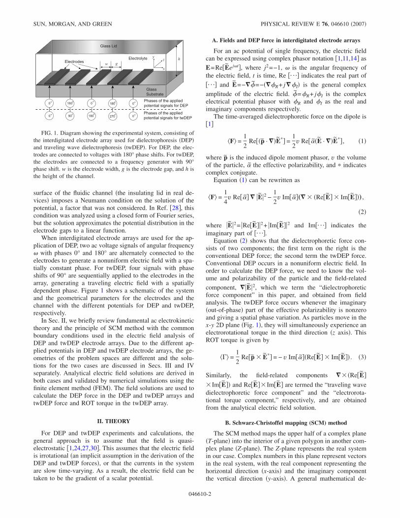
The values for the real and imaginary parts of the poten-tial phasor at each electrode, together with the boundary con-ditions are shown in Fig. 2�a�. Since the two ac signals ofangular frequency � with phases 0° and 180° are alternatelyconnected to the electrodes, the boundary conditions areequivalent to two in-phase signals with opposite sign and theimaginary part of the potential phasor is zero ��I=0� andonly the real part �R needs to be solved. From symmetry, thebasic cell �ABCDE� is chosen for the electric field analysis.For a detailed description of the boundary conditions in theDEP array, see �30�.
Figure 2�b� shows the three complex planes used for themapping procedure. The selected cell ABCDE is rotated 90°and set in the Z-plane with the boundary conditions for �R asshown: ��R /�n=0, along the insulating walls AE and CDand the boundary for the axis of even symmetry �BC�. Di-richlet boundary conditions define the fixed potential �R=Valong the electrode �AB� and the boundary for the axis of oddsymmetry, �R=0 �DE�. The complex coordinates for eachpoint in the physical plane �according to the geometrical pa-
ANALYTICAL SOLUTIONS OF AC ELECTROKINETICS IN … PHYSICAL REVIEW E 76, 046610 �2007�
046610-3
rameters of the system� are ZA= jg /2, ZB= j�w+g� /2, ZC=h+ j�w+g� /2, ZD=h, and ZE=0.
B. SCM procedure for array with lid
The interior of the polygon ABCDE in the Z-plane ismapped into the upper half of the T-plane using the SCMmethod. The polygon ABCDE is opened at point F and theboundaries of the polygon mapped to the real axis of theT-plane. The coordinates of the corresponding points ZA toZE in the T-plane are TA to TE, respectively. The point F ismapped to positive and negative infinity. The four interior
angles of polygon ABCDE at points E, B, C, D are all � /2.According to Eq. �3�, the SCM integral from T-plane toZ-plane is given by
Z = C1�T
�T − TE�−1/2�T − TB�−1/2�T − TC�−1/2�T − TD�−1/2dT
+ C2, �4�
where Z=Zx+ jZy refers to the complex coordinate of anypoint in the interior of polygon ABCDE in the Z-plane. T=Tx+ jTy refers to the complex coordinate of any point in theupper half of the T-plane.
AB
C D
E
Fh
w g
Electrodes
��
=R
n0
R V
R 0=
R =
=� =
V VV V
jVe V VjVe
( )Re ⎡ ⎤⎣ ⎦j tVe ( )Re +⎡ ⎤⎣ ⎦
j tVe Re ⎡ ⎤⎣ ⎦j tVe
R 0=
R 0=R 0= R 0=
R V R V= R V= R V= R V=R V R V
��
=R
n0
��
=R
n0
��
=R
n0
Re ⎡ ⎤⎣ ⎦j tVe
(a)
A
B C
DE Fx
y
ABCD E F+x
y
A B
DEx
y
00 1 1.2 TA TE 0 XWd
YWd
(j) (j) (j)
T-plane W-plane
(g+w)/2
g/2
h
��
=R
n0
R 0=
R V=
R V=
R V=
��
=R
n0
��
=R
n0
��
=R
n0
R 0= R 0= R 0=
��
=R
n0
��
=R
n0
��
=R
n0
Z-plane
∞ F- +∞
(b)
AB
C D
Ex
y
0
(j)
(g+w)/2w/2��
=φRn
0
φR 0=
φR V=
��
=φRn
0
Z-plane
ABC DEx
y
0-1 TA
(j)
T-planeφR V= �
�=φR
n0
��
=φRn
0 φR 0=
−∞ +∞
∞∞
A B
DEx
y
0 XWd
YWd
(j)
W-plane
φR V=
��
=φRn
0
φR 0=
��
=φRn
0
’
’
(c)
FIG. 2. �a� Schematic of a 2D section of the DEP electrode showing the potentials. The vertical lines mark the period over which thesystem repeats. The rectangle ABCDE is the basic cell for analysis. Also shown is the potential �, the potential phasor �, and the value ofthe real part of the potential phasor �R on each electrode. The imaginary part of the potential phasor �I is zero everywhere. �b� Diagramshowing the three complex planes used for Schwarz-Christoffel mapping �SCM� taking into account the lid. �c� Diagram showing the threecomplex planes used for the Schwarz-Christoffel mapping �SCM� procedure for array without the lid.
SUN, MORGAN, AND GREEN PHYSICAL REVIEW E 76, 046610 �2007�
046610-4
Since the SCM method allows up to three points to bearbitrarily chosen along the real axis of the T-plane, we fixthe coordinates of TD=0, TC=1 and TB=1.2 as shown in Fig.2�b�. For TTETBTCTD, the solution of Eq. �4� is anelliptic integral �48�:
Z = C3F�d1,kd1� + C2
= C3�0
�d1 d�d1
�1 − �d12 ��1 − kd1
2 �d12 �
d�d1 + C2, �5�
where F�d1 ,kd1� is the elliptical integral of the first kindand kd1 is the modulus of the elliptic function. The expres-sions for the variables C3, d1, kd1, and �d1 are given inAppendix B.
Equation �5� links the T-plane to the Z-plane. The valuesof the coefficients C2 and C3 can be solved by a mappingrelationship between the coordinates of the correspondingpoints in the two planes, which is shown in Appendix B:
C2 = 0, C3 =h
K�kd1�=
w + g
2K�k�d1�, �6�
where K�kd1� is the complete elliptic integral of the first kindand kd1� =1−kd1
2 . The expression for C3 also provides therelationship between the complete elliptical integral and thegeometrical parameters of the system:
K�kd1�K�k�d1�
=2h
w + g. �7�
The value of the modulus, kd1 can be calculated by inputtingarbitrary geometrical parameters using Hilberg’s approxima-tion �49�.
The inverse function of Eq. �5� enables us to express T interms of Z:
T =
TETBcn2 Z
C3,kd1�
TB − TEsn2 Z
C3,kd1� , �8�
where sn�…, …� and cn�…, …� are the Jacobian ellipticfunctions. The expression for TE is given in Appendix B andTB=1.2.
The second SCM is used to transform the upper half ofthe T-plane into a rectangle in the model plane �W-plane�.The electric field is uniformly distributed in the interior ofthe rectangle, due to the restriction from the transformedboundaries in the W-plane. The corresponding points areWA= jYWd, WB=XWd+ jYWd, WD=XWd, and WE=0, whereXWd and YWd are the size of the rectangle along the real andimaginary axis, respectively. Similarly, the transformationfrom the T-plane to the W-plane is given by
W = D1�T
�T − TE�−1/2�T − TA�−1/2�T − TB�−1/2�T − TD�−1/2dT
+ D2. �9�
It should be noted that, compared to Eq. �4�, in this transfor-
mation point A replaces C to become an angle of the rect-angle. The integral solution of Eq. �9� is
W = D3F�d2,kd2� + D2
= D3�0
�d2 d�d2
�1 − �d22 ��1 − kd2
2 �d22 �
d�d2 + D2. �10�
The expressions for D3, d2, kd2, and �d2 are given in Ap-pendix B. Equation �10� links the T-plane with the W-plane.The values of the coefficients D2 and D3 can be obtained bya similar procedure to the first SCM performance:
D2 = 0, D3 =XWd
K�kd2�=
YWd
K�k�d2�. �11�
C. Analytical electric field solution in array with lid
Since Laplace’s equation remains invariant under confor-mal mapping, the potential gradients in the physical plane,��Z, and model plane, ��W, are related by �31�
��Z = ��Wf��Z� = ��WdW
dZ. �12�
f��Z� is the conjugate of the derivative of f�Z�, which is thelinking transformation equation between the Z- andW-planes. Using this relationship and combining Eqs. �4�and �9�, the nonuniform electric field distribution in theZ-plane, EZd, can be derived as
EZd = − ��Zd = − ��WddW
dT
dT
dZ�
= jV
h
K�kd1�K�k�d2�
�TA�TE − TB��T − TC�TB�TE − TC��T − TA� 1/2
,
�13�
where �Zd and �Wd are the potentials in the Z- and W-planes,respectively, and V is the potential difference between theelectrode AB and the axis of odd symmetry, DE. Note thatthe expressions for TA and TE are given in Appendix B andTB=1.2 and TC=1.
Equation �13� is the analytical solution for the electricfield in the basic cell for the interdigitated DEP array. Com-pared to the previous analytical solution using series expan-sions, Eq. �13� is significantly simpler. The features of theelectric field distribution that are governed by the geometryof the device are clearly identified. The electric field magni-tude approaches zero at point C �when T=TC� and infinity atpoint A �when T=TA�, the edge of the electrode.
Substituting Eq. �8� into �13�, we obtain the electric fieldexpression as a function of position in the interior of polygonABCDE in the Z-plane:
ANALYTICAL SOLUTIONS OF AC ELECTROKINETICS IN … PHYSICAL REVIEW E 76, 046610 �2007�
046610-5
EZd
= jV
h
K�kd1
�
K�k�d2
�
⎩⎪⎨⎪⎧
TA�T
E− T
B�� T
ET
Bcn
2�Zx
+ Zyj
C3
,kd1�
TB
− TEsn
2�Zx
+ Zyj
C3
,kd1�
− TC�
TB�T
E− T
C�� T
ET
Bcn
2�Zx
+ Zyj
C3
,kd1�
TB
− TEsn
2�Zx
+ Zyj
C3
,kd1�
− TA�⎭⎪
⎬⎪⎫
1/2
. �14�
To calculate the DEP force in the array, we determine the
value of the dielectrophoretic force component, ��E�2:
��EZd�2 = ��EZd�x2 + EZd�y
2 � , �15�
where EZd�x and EZd�y represent the x and y components ofthe electric field in the real geometry, respectively.
Separating the real and imaginary parts of Eq. �15� to givethese components requires the formulas for the Jacobian el-liptic functions �50� �see Appendix B�.
D. Analytical electric field solution in array without lid
One common feature of previous analytical solutions�23–27� is that the upper boundary, i.e., the lid of the chan-nel, was not considered in the analysis. Instead, the potentialwas assumed to tend to zero as the height goes to infinity,which is only valid if the lid is far from the electrodes. How-ever if the height of the channel is comparable to the widthof the electrodes �and gap�, the lid will influence the electricfield distribution.
Equation �14� gives the field distribution for a fixed chan-nel height. For comparison with existing solutions we alsouse the SCM method to derive the electric field solution fora system without the lid.
The three complex planes for this case are shown in Fig.2�c�. The boundary conditions are the same as for the previ-ous case, except for the top Neumann boundary condition. Inthe Z-plane, the coordinates of each point are ZA=w /2, ZB=0, ZC=0+ j�, ZD= �w+g� /2+ j�, and ZE= �g+w� /2. TheSCM integral from the Z-plane to the T-plane is
Z = C1��T
�T − TE�−1/2�T − TB�−1/2dT + C2�. �16�
In the T-plane, the coordinates of point B and E are chosenat: TB=−1 and TE=0. The points C and D are mapped tonegative and positive infinity on the real axis of the T-planerespectively. The solution of Eq. �16� is
Z = 2C1� ln�T + T + 1� + C2�, �17�
where the coefficients C1� and C2� are obtained from applyingthe mapping to points B and E in the Z- and T-planes:
C1� = jw + g
2�, C2� =
w + g
2. �18�
The inverse function of Eq. �17� is
T = sinh2Z − C2�
2C1�� . �19�
This gives the coordinate of point A in the T-plane:
TA = sinh2 jg�
2�w + g�� . �20�
The SCM integral from the T-plane to the W-plane is
W = D1��T
�T − TE�−1/2�T − TA�−1/2�T − TB�−1/2dT + D2�.
�21�
For TTETATB the solution of Eq. �21� is an ellipticintegral �48�:
SUN, MORGAN, AND GREEN PHYSICAL REVIEW E 76, 046610 �2007�
046610-6

W = D3�F�d3,kd3� + D2�
= D3��0
�d3 d�d3
�1 − �d32 ��1 − kd3
2 �d32 �
d�d3 + D2�. �22�
with
D3� =2D1�
TE − TB
, d3 = arcsinT − TE
T − TA� ,
kd3 =TA − TB
TE − TB, �d3 = sin d3.
In the W-plane, WA= jY�Wd, WB=X�Wd+ jY�Wd, WD=X�Wd,and WE=0. The values of the coefficients D�2 and D�3 are
D2� = 0, D3� =X�Wd
K�kd3�=
Y�Wd
K�k�d3�. �23�
The nonuniform electric field distribution in the Z-plane isthen solved as
E�Zd = − ��WddW
dT
dT
dZ� =
�V
w + g
1
K�k�d3�TE − TB
T − TA�1/2
.
�24�
This is the analytical solution for the electric field in thebasic cell of the DEP electrode array without the insulatinglid. Note that TA is given by Eq. �20� and TB=−1 and TE=0. Compared to Eq. �13�, the electric field magnitude goesto infinity at the edge of the electrodes �point A�. Howeverthere is no point of zero field, since point C goes to infinityin the y direction in the Z-plane. In this paper, calculations ofthe electric fields and ��EZd�2 using Elliptic functions were
FIG. 3. The electric field and DEP force component ���EZd�2� in the basic cell of the DEP array without lid. The positions of theelectrodes are drawn on the figures. �a� Electric field vector and magnitude �V/m, log10 scale�, �b� 3D surface plot of electric field magnitude,�c� DEP force component vector and magnitude �log10 scale�, and �d� 3D surface plot of ��EZd�2.
ANALYTICAL SOLUTIONS OF AC ELECTROKINETICS IN … PHYSICAL REVIEW E 76, 046610 �2007�
046610-7

performed in MATLAB™ �Mathworks Inc, Natick, MA,USA�.
E. Electric field distribution and DEP force
Typical experimental values were used in the calculations:The electrode width and gap were 20 �m and the voltageapplied to the electrode was 1 V. For the case of the arraywith lid, the channel height was 60 �m.
Figure 3�a� shows the electric field up to 60 �m in height,for the basic cell without the lid. The magnitude of the elec-tric field is symmetrical about the vertical line through theelectrode edge, since the electrode width and the gap are thesame. Figure 3�b� shows the electric field magnitude as a 3Dsurface, clearly demonstrating the maximum �theoreticallyinfinity� at the electrode edge and the exponential decreasewith height in the far field, as reported previously �26,27,30�.
Figure 3�c� is a plot of ��EZd�2, showing that the DEP force�direction and magnitude� is symmetrical about the verticalline through the electrode edge, also due to the same lengthof the electrode width and the gap. It can also be seen that inthe far field, the DEP force acts only in the vertical directionand in the near field, ��EZd�2 points towards the electrodeedge. Figure 3�d� shows the magnitude of ��EZd�2 as a 3Dsurface, clearly showing the maximum at the electrode edge,the minima in the corners at the substrate and the exponentialdecrease with height in the far field.
Figure 4�a� shows the electric field for the array with thelid. The bending of the electric field lines by the lid is clearlyobserved in the vector plot, where the vectors near the topboundary tend to lie parallel to the lid. This clearly shows theconsequence of the Neumann boundary condition, imposedat the lid. In this case, the magnitude of the electric field isnot symmetrical about the vertical line through the electrode
FIG. 4. Solutions of the electric field and DEP force component ���EZd�2� in the basic cell of the DEP array with the lid. �a� Electric fieldvector and magnitude �V/m, log10 scale�, �b� 3D surface plot of the magnitude of the electric field, �c� DEP force component, vector, andmagnitude �log10 scale�, and �d� 3D surface plot of ��EZd�2.
SUN, MORGAN, AND GREEN PHYSICAL REVIEW E 76, 046610 �2007�
046610-8
edge, even though the electrode width and the gap are equal.This can be seen more clearly in Fig. 4�b�, the electric fieldmagnitude is zero at point C �the point where the lid meetsthe even symmetry axis�, since at this point, it has to simul-taneously satisfy the Neumann boundary condition at the lidand the even symmetry axis �CD and BC in Fig. 2�b�,Z-plane�. Close to the electrode surface, there is a maximumat the electrode edge. Figure 4�c� shows ��EZd�2 for this case,demonstrating that while the DEP force in the near field isapproximately the same as for the previous case, in the farfield �close to the lid�, the behavior is quite different. Thefield minimum in the corner has a strong influence on thedirection of the DEP force, which is no longer only in thevertical direction, and practically would result in a negativeDEP trap at point C. Figure 4�d� shows the maximum in theDEP force at the electrode edge and the four minima in eachcorner.
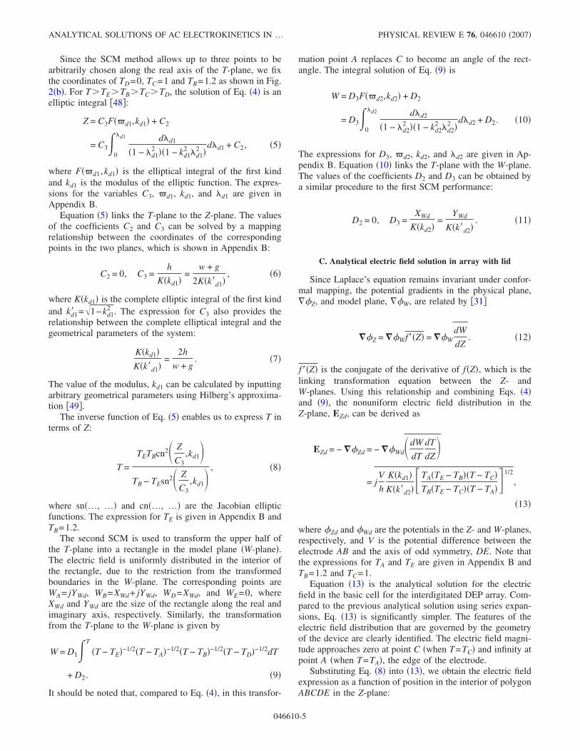
Since most analytical solutions ignore the presence of anupper boundary, a further examination of the effect of the lidis warranted. If the channel height is of the same order ofmagnitude as the electrode width and gap distance, the effectof the lid is always important. Figure 5�a� shows significantdifference in the electric field magnitude at a height of10 �m for two different channel heights, with the solutionfor a channel height of 20 �m showing considerable dis-agreement with the no lid case. The 100 �m channel heightcase agrees with the no lid situation, showing that the effectof the lid in the near field region becomes negligible as the
channel height increases. However, this effect still plays animportant role in the far field region, near the top of thechannel. This is demonstrated by Fig. 5�b�, which shows theelectric field magnitude at a height of 90 �m for the 100 �mhigh channel compared with the solution for no lid, wherethe magnitude of the field is constant. This figure shows thatthe presence of the lid cannot be ignored when determiningthe DEP force in the region close to the lid.
F. Comparisons with FEM simulations—electric field
The analytical solution for the electric field was comparedwith numerical simulations performed using COMSOL
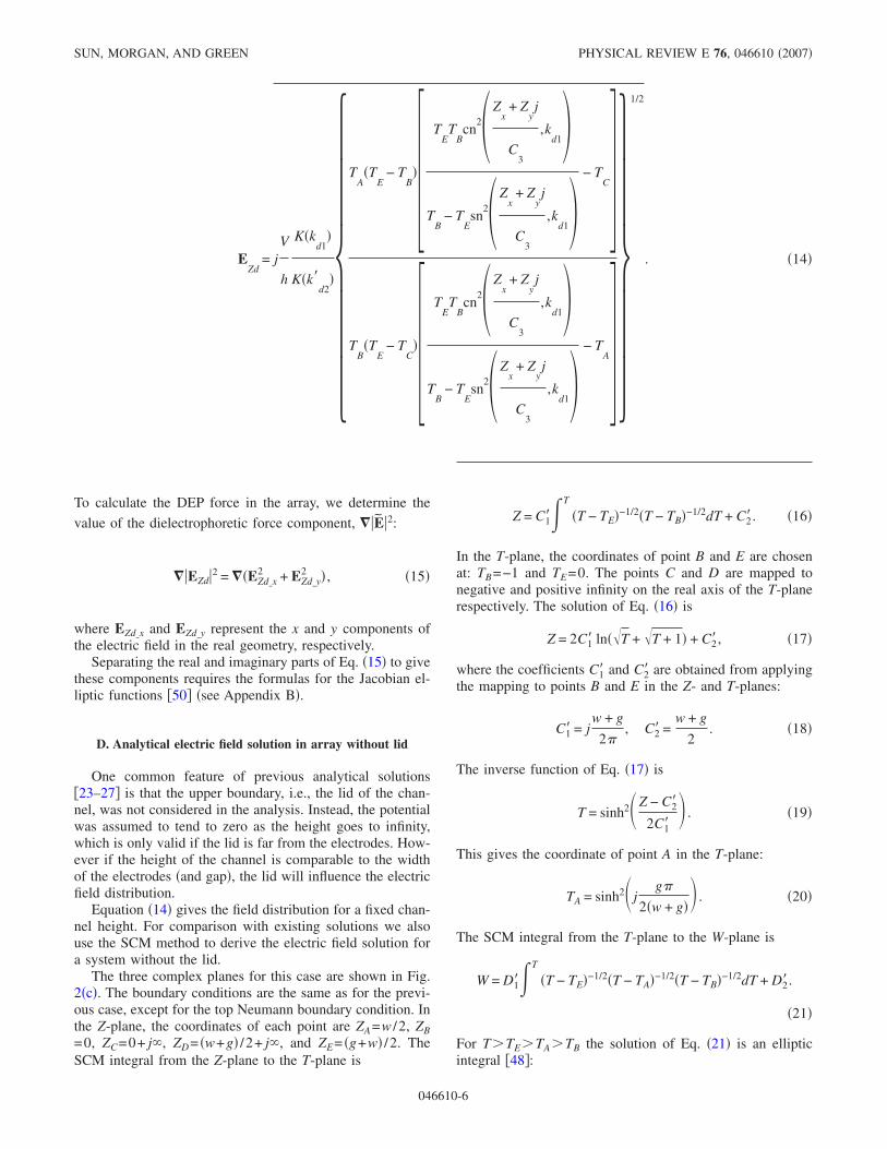
MULTIPHYSICS™ �Comsol Ltd.�, a finite element method�FEM� solver. In order to ensure the accuracy of the numeri-cal simulations, the meshing was increased around the elec-trode edge �point A�, and along paths where the electric fieldwas sampled. The analytical solutions were validated morecomprehensively by varying the ratio of the electrode widthand gap distance. For the array with lid, the height of thechannel was set to 60 �m, with the sum of electrode widthand gap fixed at 40 �m. The ratios of electrode:gap widthwere 1:3, 1:1, and 3:1 and comparisons of the electric fieldwere performed at heights of 10 �m �near field region�,30 �m �middle field region�, and 50 �m �far field region�,respectively.
Figures 6�a�–6�c� demonstrate excellent agreement be-tween the SCM solutions and the FEM solutions for the threeratios and heights detailed above. The figures also demon-strate the relationship between the electric field magnitudeand the ratio of the electrode width and gap. In the near fieldregion, Fig. 6�a�, the position of the electrode edge deter-mines the region of maximum field. By extending the edgeof the electrode towards the odd symmetry axis �DE�, thehigh field region shifts from the even symmetry axis �BC�side to the odd symmetry axis side. In the middle and farfield regions �Figs. 6�b� and 6�c��, this effect gradually dis-appears and the electric field magnitude on the odd symme-try axis side is always higher than that on the even symmetryaxis side, due to the existence of the zero field point. For thearray without lid, comparisons were performed for the sameelectrode width to gap ratios, with the channel height set to500 �m in the FEM simulations. The values of the electricfield are sampled in the near field region at a height of10 �m and the results are shown in Fig. 6�d�, again showingexcellent agreements with the analytical model.
G. Comparisons with Fourier series solutions
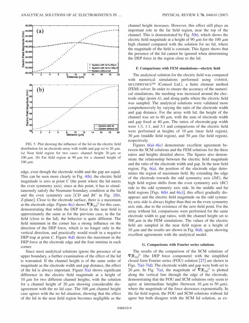
The results of the comparison of the SCM solutions of��EZd�2 �the DEP force component� with the simplifiedclosed form Fourier series �FOU� solution �27� are shown inFigs. 7�a�–7�d�. The electrode width and gap were both set to20 �m. In Fig. 7�a�, the magnitude of ��EZd�2 is plottedalong the vertical line through the edge of the electrode,demonstrating that the FOU and SCM solutions only seem toagree at intermediate heights �between 10 �m to 50 �m�,where the magnitude of the force decreases exponentially. Inthe far field region, the FOU and SCM solutions without lidagree but both disagree with the SCM lid solution, as ex-
FIG. 5. Plot showing the influence of the lid on the electric fielddistribution for an electrode array with width and gap set to 20 �m.�a� Near field region for two cases: channel height 20 �m or100 �m. �b� Far field region at 90 �m for a channel height of100 �m.
ANALYTICAL SOLUTIONS OF AC ELECTROKINETICS IN … PHYSICAL REVIEW E 76, 046610 �2007�
046610-9
0 2 4 6 8 10 12 14 16 18 2024,000
28,000
32,000
36,000
40,000
44,000
48,000
52,000
56,000
Distance ( m)
Elec
tric
Fiel
dM
agn
itu
de
(V/m
)SCM w=10 m, g=30 m
FEM w=10 m, g=30 mSCM w=20 m, g=20 mFEM w=20 m, g=20 mSCM w=30 m, g=10 m
FEM w=30 m, g=10 m
h=60 mnear field region
0 2 4 6 8 10 12 14 16 18 206,000
6,400
6,800
7,200
7,600
8,000
8,400
8,800
9,200
9,600
Distance ( m)
Elec
tric
Fiel
dM
agn
itu
de
(V/m
)
SCM w=10 m, g=30 m
FEM w=10 m, g=30 m
SCM w=20 m, g=20 m
FEM w=20 m, g=20 m
SCM w=30 m, g=10 m
FEM w=30 m, g=10 m
h=60 mmiddle field region
0 2 4 6 8 10 12 14 16 18 201000
1200
1400
1600
1800
2000
2,200
2,400
Distance ( m)
Elec
tric
Fiel
dM
agn
itu
de
(V/m
)
SCM w=10 m, g=30 mFEM w=10 m, g=30 mSCM w=20 m, g=20 mFEM w=20 m, g=20 mSCM w=30 m, g=10 mFEM w=30 m, g=10 m
h=60 mfar field region
0 2 4 6 8 10 12 14 16 18 2025,000
30,000
35,000
40,000
45,000
50,000
55,000
Distance ( m)
Elec
tric
Fiel
dM
agn
itu
de
(V/m
)
SCM w=10 m, g=30 mFEM w=10 m, g=30 mSCM w=20 m, g=20 mFEM w=20 m, g=20 mSCM w=30 m, g=10 mFEM w=30 m, g=10 m
No lid casenear field region
(a)
(b)
(c) (d)
FIG. 6. Plot showing the electric field distribution from the SCM solutions and FEM simulations for different geometries. �a� Near fieldregion, with lid �b� midfield region, with lid �c� far field region, with lid �d� near field region, no lid.
0 2 4 6 8 10 12 14 16 18 202
2.5
3
3.5
4 x 10¹⁴
Distance ( m)
DEP
Forc
eC
om
po
nen
t
Mag
nit
ud
e(V
2/m
3)
SCM solution with lidSCM solution no lidFourier series solution
w=g=20 m, h=20 m
0 2 4 6 8 10 12 14 16 18 201013
1014
1015
1016
Channel Height ( m)
DEP
Forc
eC
om
po
nen
t
Mag
nit
ud
e(V
2/m
3)
SCM solution with lidSCM solution no lidFourier series solution
w=g=20 m, h=20 m
0 2 4 6 8 10 12 14 16 18 202
2.5
3
3.5
4 x 10¹⁴
Distance ( m)
DEP
Forc
eC
om
po
nen
t
Mag
nit
ud
e(V
2/m
3)
SCM solution with lidSCM solution no lidFourier series solution
w=g=20 m, h=60 m
0 10 20 30 40 50 601010
1011
1012
1013
1014
1015
1016
Channel Height ( m)
DEP
Forc
eC
om
po
nen
t
Mag
nit
ud
e(V
2/m
3)
SCM solution with lidSCM solution no lidFourier series solution
w=g=20 m, h=60 m
(a) (b)
(c) (d)
FIG. 7. Comparison of the DEP force component ���EZd�2� calculated by the SCM and Fourier series solutions. �a� Magnitude calculatedalong a vertical line through the edge of the electrode, 60 �m channel height; �b� Magnitude calculated along a horizontal line at a heightof 10 �m, 60 �m channel height; �c� Magnitude calculated along a vertical line through the edge of the electrode, 20 �m channel height;�d� Magnitude calculated along the horizontal line at height of 10 �m, 20 �m channel height.
SUN, MORGAN, AND GREEN PHYSICAL REVIEW E 76, 046610 �2007�
046610-10

pected due to the neglected upper boundary condition. In thenear field solution, the SCM solutions with and without lidagree with each other but deviation of the FOU solution isreadily apparent. Calculation of the magnitude of ��EZd�2along a horizontal line at a height of 10 �m, Fig. 7�b�, showsthat the FOU solution is not symmetrical about the verticalline through the edge of the electrode as observed in thevector plot in Fig. 5 of �27�. For low channels, the FOUsolution is even more inaccurate, since the effect of the lid ismore pronounced, as shown in Figs. 7�c� and 7�d�.
A quantitative discussion of the difference between thetwo solution methods can be performed by examining thedifference in magnitude and the angle of deviation in direc-tion. The magnitude difference was determined as the ratio:FFOU/FSCM, where FFOU and FSCM are the magnitude of theDEP forces for the two solutions. The deviation between thedirections of the force vectors was characterized by cos ,defined as
cos =FFOU · FSCM
�FFOU��FSCM�. �25�
Figure 8�a� shows a surface plot of the magnitude of
FFOU/FSCM. At the electrode edge, the magnitude of the DEPforce from the Fourier series is approximately one order ofmagnitude less than that given by the SCM solution. How-ever, at the three corners of the basic cell �except the corneron the surface of the electrode�, the Fourier series solution isapproximately two orders of magnitude greater than theSCM solution. In the mid range of height, Fig. 8�b� showsthat even where the agreement was apparently good in Fig.7�a�, the difference is still approximately 15%. Figure 8�c�shows the surface plot of cos , demonstrating the misalign-ment between the direction of the DEP force in the FOU andSCM solutions in the far field region �close to the lid� andthe near field region in the gap.
IV. TRAVELING WAVE DIELECTROPHORETICELECTRODE ARRAY
In the twDEP electrode array, since the four signals arephase shifted by 90° and are connected alternately to theelectrodes, both the real and imaginary parts of the potentialphasor must be considered.
A. Boundary conditions
Apart from the common boundary conditions, the valuesfor the real and imaginary parts of the potential phasor atevery electrode and the additional boundary conditions areshown in Fig. 9�a�. The basic cell �ABCDEF� chosen foranalyzing the electric field distribution covers the region be-tween the centers of two adjacent electrodes and the entiregap between. According to Fig. 9�a�, the boundary conditionsfor the imaginary part of the potential phasor, �I, are themirror image of those for the real part, �R, about the centerof the gap. This indicates that only the real component of thepotential, i.e., for ER, must be solved, which can then betransformed to give the solution for the imaginary compo-nent.
Figure 9�b� shows the three complex planes used in theSCM method to solve the real part of the electric field. In theZ-plane, which represents the real system, the basic cellABCDEF is rotated 90°. The complete boundary conditionsfor the real part of the potential phasor, �R, are as shown.The Neumann boundary condition ��R /�n=0 �indicated bydashed lines� holds along the insulating walls AF and CD aswell as the axis of even symmetry, BC. Dirichlet boundaryconditions define the fixed potential �R=V on the electrodeAB and �R=0 on the electrode EF, as well as �R=0 on theaxis of odd symmetry, DE. The coordinates of each point inthe physical plane are ZA= j�2g+w� /2, ZB= j�w+g�, ZC=h+ j�w+g�, ZD=h, ZE=0, and ZF= jw /2.
B. SCM procedure
In the auxiliary plane �the T-plane�, the polygonABCDEF is opened at point G in the Z-plane and mappedinto the upper half of the T-plane, with all the boundariesmapped onto the real axis. The coordinates of the corre-sponding points to ZA , . . . ,ZF in the T-plane are TA , . . . ,TF,respectively. The point G is mapped to positive and negative
05
1015
20
0
20
40
600
0.5
1
1.5
( m)
cos
Electrode Edge(c)
Distance ( m)Channel Height
05
1015
20
020
4060
10−1
100
101
102
Distance (µm)Channel Height ( µm)
FF
OU
/FS
CM
Electrode Edge(a)
0 10 20 30 40 50 600
0.20.40.60.8
11.21.41.61.8
22.22.42.6
Channel Height ( m)
FF
OU
/FS
CM
x=5 mx=10 m (Edge of Electrode)x=15 m
(b)
xy
xy
FIG. 8. �a� Surface plot of the magnitude of the ratio of the DEPforce from the Fourier solution �FFOU� and SCM solution �FSCM�,with lid, for 60 �m high channel, 20 �m electrode width and gap.�b� Plot of the value of the magnitude of the ratio �FFOU/FSCM�along three vertical lines �x=5, 10, and 15 �m�. �c� Surface plot ofthe deviation of the direction �cos � between the DEP force fromthe Fourier solution �FFOU� and SCM solution �FSCM�, with lid. Thealignment of the two solutions is only achieved, when =0°, lead-ing to cos =1.
ANALYTICAL SOLUTIONS OF AC ELECTROKINETICS IN … PHYSICAL REVIEW E 76, 046610 �2007�
046610-11
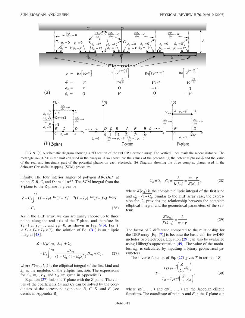
infinity. The four interior angles of polygon ABCDEF atpoints E, B, C, and D are all � /2. The SCM integral from theT-plane to the Z-plane is given by
Z = C1�T
�T − TE�−1/2�T − TB�−1/2�T − TC�−1/2�T − TD�−1/2dT
+ C2. �26�
As in the DEP array, we can arbitrarily choose up to threepoints along the real axis of the T-plane, and therefore fixTB=1.2, TC=1, and TD=0, as shown in Fig. 9�b�. For TTETBTCTD, the solution of Eq. �B1� is an ellipticintegral �48�:
Z = C3F�t1,kt1� + C2
= C3�0
�t1 d�t1
�1 − �t12 ��1 − kt1
2 �t12 �
d�t1 + C2, �27�
where F�t1 ,kt1� is the elliptical integral of the first kind andkt1 is the modulus of the elliptic function. The expressionsfor C3, t1, kt1, and �t1 are given in Appendix B.
Equation �27� links the T-plane with the Z-plane. The val-ues of the coefficients C2 and C3 can be solved by the coor-dinates of the corresponding points: B, C, D, and E �seedetails in Appendix B�
C2 = 0, C3 =h
K�kt1�=
w + g
K�k�t1�, �28�
where K�kt1� is the complete elliptic integral of the first kindand kt1� =1−kt1
2 . Similar to the DEP array case, the expres-sion for C3 provides the relationship between the completeelliptical integral and the geometrical parameters of the sys-tem:
K�kt1�K�k�t1�
=h
w + g. �29�
The factor of 2 difference compared to the relationship forthe DEP array �Eq. �7�� is because the basic cell for twDEPincludes two electrodes. Equation �29� can also be evaluatedusing Hilberg’s approximation �49�. The value of the modu-lus, kt1, is calculated by inputting arbitrary geometrical pa-rameters.
The inverse function of Eq. �27� gives T in terms of Z:
T =
TETBcn2 Z
C3,kt1�
TB − TEsn2 Z
C3,kt1� , �30�
where sn�…, …� and cn�…, …� are the Jacobian ellipticfunctions. The coordinate of point A and F in the T-plane can
⎡ ⎤⎡ ⎤
⎡ ⎤
AB
C D
EF
h
wg
G
Electrodes
φR 0=
��
=φRn
0
φR VφR V=
��
=φRn
0
φR 0=φR 0= φI 0=
��
=φIn
0
φI V=
��
=φIn
0��
=φIn
0
φI 0=φR 0=φI V= φR V
φI 0=φI VφI V φR V=
φI 0=
φR =
φ =
�φ =
( )Re j tVe +⎣ ⎦Re j tVe⎡ ⎤
⎣ ⎦
V−V−V
V
V jVe
2Rej t
Ve⎛ ⎞+⎜ ⎟⎝ ⎠⎢ ⎥
⎢ ⎥⎣ ⎦
32Re
j tVe
⎛ ⎞+⎜ ⎟⎝ ⎠⎢ ⎥
⎢ ⎥⎣ ⎦
φI =
2j
Ve32j
Ve
(a)
A
B
DEF
x
y
ABCD EFx
y
A B
DFx
y
00 1 TA TE 0 XWd
YWd
(j) (j) (j)
Z-plane T-plane W-plane
g+w(2g+w)/2
hG
C
w/2
TF
��
=φRn
0
��
=φRn
0
��
=φRn
0
��
=φRn
0 ��
=φRn
0
��
=φRn
0 ��
=φRn
0
φR V=
φR V=
φR V=
φR 0=
φR 0=φR 0= φR 0= φR 0=
G+ +∞−∞ G-
1.2
(b)
00
00
FIG. 9. �a� A schematic diagram showing a 2D section of the twDEP electrode array. The vertical lines mark the repeat distance. Therectangle ABCDEF is the unit cell used in the analysis. Also shown are the values of the potential �, the potential phasor � and the valueof the real and imaginary part of the potential phasor on each electrode. �b� Diagram showing the three complex planes used in theSchwarz-Christoffel mapping �SCM� procedure.
SUN, MORGAN, AND GREEN PHYSICAL REVIEW E 76, 046610 �2007�
046610-12

be obtained from Eq. �30� �see Appendix B�.The SCM method is then used a second time, with the
upper half of the T-plane transformed into a rectangle in themodel plane �W-plane�, where the electric field distribution isuniform. The four corner points in the W-plane are: WA= jYWt, WB=XWt+ jYWt, WD=XWt and WF=0 where XWt andYWt are the size of the region along the real and imaginaryaxes, respectively. The transformation from the T-plane tothe W-plane is given by
W = D1�T
�T − TF�−1/2�T − TA�−1/2�T − TB�−1/2�T − TD�−1/2dT
+ D2. �31�
It should be noted that compared to Eq. �26�, in this trans-formation points A and F replace C and E to become twocorners of the rectangle. The integral solution of Eq. �31� is
W = D3F�t2,kt2� + D2
= D3�0
�t2 d�t2
�1 − �t22 ��1 − kt2
2 �t22 �
d�t2 + D2, �32�
with
D3 =2D1
�TA − TD��TF − TB�,
t2 = arcsin�TA − TD��T − TF��TF − TD��T − TA�
� ,
kt2 =�TF − TD��TA − TB��TA − TD��TF − TB�
, �t2 = sin t2.
Equation �32� gives the transformation from the T-plane toW-plane. The values of the coefficients D2 and D3 can beobtained by a similar point-point mapping procedure as pre-sented in Appendix B for the first SCM transformation:
D2 = 0, D3 =XWt
K�kt2�=
YWt
K�k�t2�. �33�
C. Analytical electric field solution
Using the relationship between the gradient of the poten-tial in the Z- and W-planes �42� and combining Eqs. �26� and�31�, the real part of the electric field distribution in theZ-plane, EZRt, for the twDEP array can be derived as
EZRt = − ��ZRt = − ��WRtdW
dZ�
= jV
h
K�kt1�K�k�t2�
�TA�TF − TB��T − TC��T − TE�TB�TE − TC��T − TA��T − TF� 1/2
,
�34�
where �ZRt and �WRt are the real part of the potential in theZ- and W-plane, respectively.
Equation �34� is the analytical solution for the real part ofthe electric field distribution in the basic cell for the twDEP
array. The expressions for TA, TE, and TF are given in Ap-pendix B and TB=1.2, TC=1. Similar features of the fielddistribution can be seen as for the DEP array case. The elec-tric field magnitude goes to zero at points C and E �whenT=TC and T=TE� and infinity at points A and F �when T=TA and T=TF�, which represent the electrode edges.
Equation �34� is then used to calculate the electric fieldterms in the expressions for the dielectrophoretic force, thetraveling wave dielectrophoretic force and electrorotationaltorque. The calculations were performed in MATLAB™. Forthe twDEP array case, we only consider a design of arraywhich includes the lid of the channel. A simpler solution withthe channel height going to infinity can be derived, as in theDEP array case, but will not be presented here. The width ofthe electrode and the gap separation was set to 20 �m andthe height of the channel to 60 �m. The voltage applied tothe electrode is 1 volt.
D. Electric field distribution
Figure 10�a� shows the direction and the magnitude of thereal part of the electric field, EZRt, for the basic cell. Figure10�b� is a 3D surface plot of the magnitude of the real part ofthe electric field, which goes to a maximum at the edge of
FIG. 10. Solutions of the real part of the electric field in thebasic cell of the twDEP array. The positions of the electrodes aredrawn on the figures. �a� Electric field vectors and magnitude �V/m,log10�. �c� 3D surface plot of electric field magnitude �V/m, log10�.
ANALYTICAL SOLUTIONS OF AC ELECTROKINETICS IN … PHYSICAL REVIEW E 76, 046610 �2007�
046610-13

the electrodes �points A and F� and decreases away from theelectrodes. The zero field points �point C and E� can clearlybe seen in the figure. The solution of EZIt, required to cor-rectly determine the forces and torques in the array, is ob-tained by mirroring the solution for EZRt about the verticalline through the horizontal position 20 �m.
E. DEP and twDEP force
Figure 11�a� shows the direction and the magnitude of��EZt�2 in the basic cell. The behavior is similar to the solu-tion presented for the DEP case. Above a certain height, thedirections of the DEP force at every position points straighttoward the electrode plane, with an exponentially decreasingmagnitude. However, as in the DEP array with completeboundary conditions, the channel lid disturbs this behaviorand the DEP force is horizontal at the lid. Figure 11�b� showsthe 3D surface plot of the magnitude of ��EZt�2, clearlyshowing the maxima at the edges of the electrode and theexponential decreases away from the electrodes. The minimain the center of the electrodes and the gap can also be seen,as well as corresponding minima at the insulating lid.
Figure 11�c� shows the direction and the magnitude of thetwDEP force component ��� �EZRt�EZIt��. Far from theelectrodes �above 10 �m�, the vectors point in the negativex-direction �left�. Approaching the bottom, the vectors point
in the opposite direction. In the region directly above theedges of the electrode, the vectors show a circular pattern, anobservation identical to previous numerical simulations �30�.From the plot of the magnitude, it is observed that the dis-tribution of the twDEP force component is more complicatedthan the DEP force. There are three twDEP force minima inthe near field region �approximately at a height of 10 �m�.Along the surface of the electrode, the magnitude of twDEPforce increases towards the edge of the electrode. However,it does not go to a maximum above the edge of the elec-trodes. Instead, it rapidly drops to a minimum over the elec-trode edge because the vectors are recirculating in this re-gion. This can be observed more clearly in the 3D surfaceplot, as shown in Fig. 11�d�.
F. ROT torque
The field term in electrorotation, which we will refer to asthe ROT torque component, is EZRt�EZIt. Figures 12�a� and12�b� show the magnitude of the ROT torque in 2D and 3Dplots, respectively. The direction of the torque is in the thirddimension �i.e., out of the page�. The magnitude of thetorque goes to a maximum at the edge of the electrode. Be-yond the near field region, the magnitude of torque decreaseswith distance from the electrode.
FIG. 11. Solutions of the DEP force component ���EZt�2� and twDEP force component ��� �EZRt�EZIt�� in the basic cell of the twDEParray. �a� DEP force component, vectors, and magnitude �log10�. �b� 3D surface plot of the magnitude of the DEP force component �log10�.�c� twDEP force component, vectors, and magnitude �log10�. �d� 3D surface plot of the magnitude of the twDEP force component.
SUN, MORGAN, AND GREEN PHYSICAL REVIEW E 76, 046610 �2007�
046610-14

G. Comparison with FEM simulations
The analytical solution for the real part of the electric fieldwas compared with numerical simulations, performedusing the finite element method �FEM� in COMSOL
MULTIPHYSICS™. The comparisons are performed by varyingthe ratio of the electrode width and gap, with the channelheight set at 60 �m. The sum of the electrode width and gapis fixed at 40 �m, with the ratio of electrode width to gapdistance varied from 1:3 �w=10 �m, g=30 �m�, 1:1 �w=20 �m, g=20 �m�, and 3:1 �w=30 �m, g=10 �m�. Com-parisons of the electric field magnitude are performed at theheight of 10 �m �near field region�, 30 �m �middle fieldregion�, and 50 �m �far field region�, respectively. Figures13�a�–13�c� show excellent agreements between the SCMsolutions and FEM solutions for the three ratios and the threeregions, respectively. This plot validates the analytical solu-
tions for the DEP, twDEP force, and ROT torque in the trav-eling wave interdigitated electrode arrays.
V. CONCLUSION
In this paper, the analytical solutions for the electric fielddistributions above interdigitated electrode arrays used fordielectrophoresis and traveling wave dielectrophoresis havebeen derived using the Schwarz-Christoffel mappingmethod. The analytical solutions for electric field for theDEP and twDEP arrays are related to the geometrical con-stant of the device: electrode length, gap distance and thechannel height. The field solutions are then used to determinethe DEP force, twDEP force, and ROT torque in the corre-sponding system. The analytical electric field solutions inboth cases are validated by comparison with the finite ele-
FIG. 12. Solutions of the ROT torque component �EZRt�EZIt�in the basic cell of the twDEP array. �a� Magnitude of the ROTtorque component magnitude in 2D. �b� 3D surface plot of themagnitude of the ROT torque.
0 5 10 15 20 25 30 35 4010,000
15,000
20,000
25,000
30,000
35,000
40,000
Distance ( m)
Elec
tric
Fiel
dM
agn
itu
de
(V/m
)
SCM w=10 m, g=30 mFEM w=10 m, g=30 mSCM w=20 m, g=20 mFEM w=20 m, g=20 mSCM w=30 m, g=10 mFEM w=30 m, g=10 m
h=60 mnear field region
0 5 10 15 20 25 30 35 407500
8000
8500
9000
9500
10000
10500
11000
Distance ( m)El
ectr
icFi
eld
Mag
nit
ud
e(V
/m)
SCM w=10 m, g=30 m
FEM w=10 m, g=30 m
SCM w=20 m, g=20 m
FEM w=20 m, g=20 m
SCM w=30 m, g=10 m
FEM w=30 m, g=10 m
h=60 mmiddle field region
0 5 10 15 20 25 30 35 402000
2500
3000
3500
4000
4500
5000
5500
6000
6500
7000
Distance ( m)
Elec
tric
Fiel
dM
agn
itu
de
(V/m
)
SCM w=10 m, g=30 mFEM w=10 m, g=30 mSCM w=20 m, g=20 mFEM w=20 m, g=20 mSCM w=30 m, g=10 mFEM w=30 m, g=10 m
h=60 mfar field region
(a)
(b)
(c)
FIG. 13. Plot showing excellent agreements between the electricfield distribution calculated with the SCM method and FEM simu-lations for different geometries. �a� Near field region, �b� midfieldregion, and �c� far field region.
ANALYTICAL SOLUTIONS OF AC ELECTROKINETICS IN … PHYSICAL REVIEW E 76, 046610 �2007�
046610-15

ment method, for different geometries, showing excellentagreement. This represents the first complete analytical elec-tric field solutions for these interdigitated electrode arrayswithout any approximation to the boundary conditions.These solutions are straightforward and easy to use and willprovide a significant improvement in field modeling and aidin modeling for the translational movement of particles inreal systems.
ACKNOWLEDGMENTS
The work is partly supported by the funding from the LifeScience Initiative of the University of Southampton. The au-thors would like to thank Antonio Ramos for useful discus-sions.
APPENDIX A: SCHWARZ-CHRISTOFFELMAPPING METHOD
In this appendix, we give the general mathematical de-scription of Schwarz-Christoffel mapping �SCM� method.Details can be found in �31�.
Let � be an m-sided polygon in the Z-plane with verticesZ1 ,Z2 . . . ,Zm and interior angles 1 , 2 , . . . , m, respectively.Along the real axis of the T-plane, T1 ,T2 , . . . ,Tm are thecorresponding mapping points to Z1 ,Z2 , . . . ,Zm in theZ-plane. The SCM integral, which maps the upper half of theT-plane into the interior of � in the Z-plane, is given by
Z = C1�T0
T
�r=1
m
�T − Tr�� r/�−1�dT + C2, �A1�
where C1 and C2 are integral coefficients. C1 establishes thescale and orientation of the polygon in the Z-plane and C2gives its position. These coefficients can be determined fromthe positions of the corresponding points in the Z- andT-planes. The mapping system has three degrees of freedomwhich means up to three points can be chosen arbitrarilyalong the real axis of the T-plane. The point T0 is the refer-ence point, which is usually chosen to be the origin.
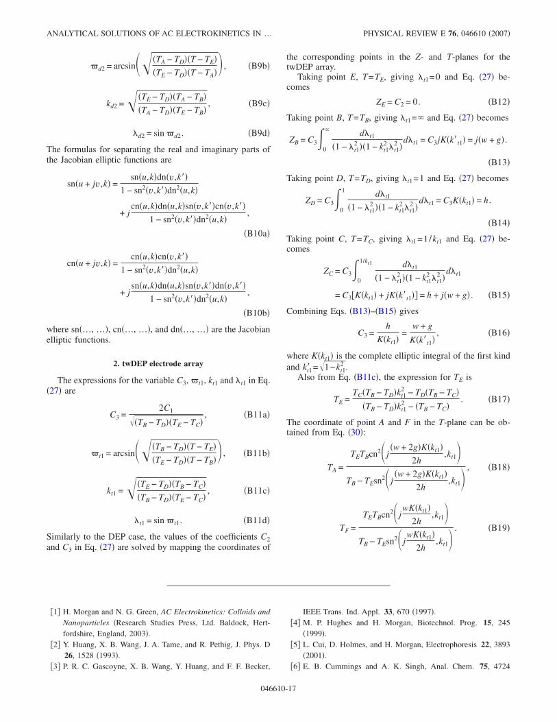
APPENDIX B: MAPPING CALCULATIONS IN THEANALYSIS OF DEP AND twDEP ARRAYS
In this appendix, the detailed calculations to determine thecoordinates of the mapping points in the DEP and twDEParrays are presented.
1. The DEP electrode array
The expressions of the variable C3, d1, kd1, and �d1 inEq. �5� are
C3 =2C1
�TB − TD��TE − TC�, �B1a�
d1 = arcsin�TB − TD��T − TE��TE − TD��T − TB�
� , �B1b�
kd1 =�TE − TD��TB − TC��TB − TD��TE − TC�
, �B1c�
�d1 = sin d1. �B1d�
The values of the coefficients C2 and C3 in Eq. �5� are solvedby mapping the coordinates of the corresponding points inthe Z- and T-planes.
Taking point E, T=TE, giving �d1=0 and Eq. �5� becomes
ZE = C2 = 0. �B2�
Taking point B, T=TB, giving �d1=� and Eq. �5� becomes
ZB = C3�0
� d�d1
�1 − �d12 ��1 − kd1
2 �d12 �
d�d1 = C3jK�kd1� � = jw + g
2.
�B3�
Taking point D, T=TD, giving �d1=1 and Eq. �5� becomes
ZD = C3�0
1 d�d1
�1 − �d12 ��1 − kd1
2 �d12 �
d�d1 = C3K�kd1� = h .
�B4�
Taking point C, T=TC, giving �d1=1/kd1 and Eq. �5� be-comes
ZC = C3�0
1/kd1 d�d1
�1 − �d12 ��1 − kd1
2 �d12 �
d�d1
= C3�K�kd1� + jK�k�d1�� = h + jw + g
2. �B5�
Combining Eqs. �B3�–�B5� gives
C3 =h
K�kd1�=
w + g
2K�k�d1�, �B6�
where K�kd1� is the complete elliptic integral of the first kindand kd1� =1−kd1
2 .Since the value of kd1 can be derived from Eq. �7�, ac-
cording to Eq. �B1� the value of TE is given by
TE =TC�TB − TD�kd1
2 − TD�TB − TC��TB − TD�kd1
2 − �TB − TC�. �B7�
Then the coordinate of point A in the T-plane can be ob-tained from Eq. �8�:
TA =
TETBcn2 jgK�k�d1�
w + g,kd1�
TB − TEsn2 jgK�k�d1�
w + g,kd1� . �B8�
The expressions of the variable D3, d2, kd2 and �d2 in Eq.�10� are
D3 =2D1
�TA − TD��TE − TB�, �B9a�
SUN, MORGAN, AND GREEN PHYSICAL REVIEW E 76, 046610 �2007�
046610-16
d2 = arcsin�TA − TD��T − TE��TE − TD��T − TA�
� , �B9b�
kd2 =�TE − TD��TA − TB��TA − TD��TE − TB�
, �B9c�
�d2 = sin d2. �B9d�
The formulas for separating the real and imaginary parts ofthe Jacobian elliptic functions are
sn�u + jv,k� =sn�u,k�dn�v,k��
1 − sn2�v,k��dn2�u,k�
+ jcn�u,k�dn�u,k�sn�v,k��cn�v,k��
1 − sn2�v,k��dn2�u,k�,
�B10a�
cn�u + jv,k� =cn�u,k�cn�v,k��
1 − sn2�v,k��dn2�u,k�
+ jsn�u,k�dn�u,k�sn�v,k��dn�v,k��
1 − sn2�v,k��dn2�u,k�,
�B10b�
where sn�…, …�, cn�…, …�, and dn�…, …� are the Jacobianelliptic functions.
2. twDEP electrode array
The expressions for the variable C3, t1, kt1 and �t1 in Eq.�27� are
C3 =2C1
�TB − TD��TE − TC�, �B11a�
t1 = arcsin�TB − TD��T − TE��TE − TD��T − TB�
� , �B11b�
kt1 =�TE − TD��TB − TC��TB − TD��TE − TC�
, �B11c�
�t1 = sin t1. �B11d�
Similarly to the DEP case, the values of the coefficients C2and C3 in Eq. �27� are solved by mapping the coordinates of
the corresponding points in the Z- and T-planes for thetwDEP array.
Taking point E, T=TE, giving �t1=0 and Eq. �27� be-comes
ZE = C2 = 0. �B12�
Taking point B, T=TB, giving �t1=� and Eq. �27� becomes
ZB = C3�0
� d�t1
�1 − �t12 ��1 − kt1
2 �t12 �
d�t1 = C3jK�k�t1� = j�w + g� .
�B13�
Taking point D, T=TD, giving �t1=1 and Eq. �27� becomes
ZD = C3�0
1 d�t1
�1 − �t12 ��1 − kt1
2 �t12 �
d�t1 = C3K�kt1� = h .
�B14�
Taking point C, T=TC, giving �t1=1/kt1 and Eq. �27� be-comes
ZC = C3�0
1/kt1 d�t1
�1 − �t12 ��1 − kt1
2 �t12 �
d�t1
= C3�K�kt1� + jK�k�t1�� = h + j�w + g� . �B15�
Combining Eqs. �B13�–�B15� gives
C3 =h
K�kt1�=
w + g
K�k�t1�, �B16�
where K�kt1� is the complete elliptic integral of the first kindand kt1� =1−kt1
2 .Also from Eq. �B11c�, the expression for TE is
TE =TC�TB − TD�kt1
2 − TD�TB − TC��TB − TD�kt1
2 − �TB − TC�. �B17�
The coordinate of point A and F in the T-plane can be ob-tained from Eq. �30�:
TA =
TETBcn2 j�w + 2g�K�kt1�
2h,kt1�
TB − TEsn2 j�w + 2g�K�kt1�
2h,kt1� , �B18�
TF =
TETBcn2 jwK�kt1�
2h,kt1�
TB − TEsn2 jwK�kt1�
2h,kt1� . �B19�
�1� H. Morgan and N. G. Green, AC Electrokinetics: Colloids andNanoparticles �Research Studies Press, Ltd. Baldock, Hert-fordshire, England, 2003�.
�2� Y. Huang, X. B. Wang, J. A. Tame, and R. Pethig, J. Phys. D26, 1528 �1993�.
�3� P. R. C. Gascoyne, X. B. Wang, Y. Huang, and F. F. Becker,
IEEE Trans. Ind. Appl. 33, 670 �1997�.�4� M. P. Hughes and H. Morgan, Biotechnol. Prog. 15, 245
�1999�.�5� L. Cui, D. Holmes, and H. Morgan, Electrophoresis 22, 3893
�2001�.�6� E. B. Cummings and A. K. Singh, Anal. Chem. 75, 4724
ANALYTICAL SOLUTIONS OF AC ELECTROKINETICS IN … PHYSICAL REVIEW E 76, 046610 �2007�
046610-17

�2003�.�7� B. H. Lapizco-Encinas, B. A. Simmons, E. B. Cummings, and
Y. Fintschenko, Anal. Chem. 76, 1571 �2004�.�8� J. Voldman, Annu. Rev. Biomed. Eng. 8, 425 �2006�.�9� H. A. Pohl, Dielectrophoresis �Cambridge University Press,
New York, 1978�.�10� B. H. Lapizco-Encinas, R. V. Davalos, B. A. Simmons, E. B.
Cummings, and Y. Fintschenko, J. Microbiol. Methods 62,317 �2005�.
�11� J. P. Huang, K. W. Yu, and G. Q. Gu, Phys. Lett. A 300, 385�2002�.
�12� G. Liao, I. I. Smalyukh, J. R. Kelly, O. D. Lavrentovich, andA. Jakli, Phys. Rev. E 72, 031704 �2005�.
�13� H. Morgan, N. G. Green, M. P. Hughes, W. Monaghan, and T.C. Tan, J. Micromech. Microeng. 7, 65 �1997�.
�14� L. Cui and H. Morgan, J. Micromech. Microeng. 10, 72�2000�.
�15� H. Kawamoto, K. Seki, and N. Kuromiya, J. Phys. D 39, 1249�2006�.
�16� N. G. Green and H. Morgan, J. Phys. Chem. B 103, 41 �1999�.�17� I. Ermolina and H. Morgan, J. Colloid Interface Sci. 285, 419
�2005�.�18� S. Archer, H. Morgan, and J. F. Rixon, J. Biol. Phys. 76, 2833
�1999�.�19� C. Dalton, A. D. Goater, J. P. H. Burt, and H. V. Smith, J.
Appl. Microbiol. 96, 24 �2004�.�20� X.-B. Wang, R. Pethig, and T. B. Jones, J. Phys. D 25, 905
�1992�.�21� X.-B. Wang, Y. Huang, R. Holzel, J. P. H. Burt, and R. Pethig,
J. Phys. D 26, 312 �1993�.�22� S. Masuda, M. Washizu, and I. Kawabata, IEEE Trans. Ind.
Appl. 24, 214 �1988�.�23� X. Wang, X.-B. Wang, F. F. Becker, and P. R. C. Gascoyne, J.
Phys. D 29, 1649 �1996�.�24� M. Garcia and D. S. Clague, J. Phys. D 33, 1747 �2000�.�25� E. Liang, R. L. Smith, and D. S. Clague, Phys. Rev. E 70,
066617 �2004�.�26� D. S. Clague and E. K. Wheeler, Phys. Rev. E 64, 026605
�2001�.�27� H. Morgan, A. G. Izquierdo, D. Bakewell, N. G. Green, and A.
Ramos, J. Phys. D 34, 1553 �2001�.�28� D. E. Chuang, S. Loire, and I. Mezic, J. Phys. D 36, 3073
�2003�.�29� X.-B. Wang, Y. Huang, J. P. H. Burt, G. H. Markx, and R.
Pethig, J. Phys. D 26, 1278 �1993�.�30� N. G. Green, A. Ramos, and H. Morgan, J. Electrost. 56, 235
�2002�.�31� R. Schinzinger and P. A. A. Laurra, Conformal Mapping:
Methods and Applications �Dover Publications, Inc., Mineola,NY, 2003�.
�32� C. K. Ikoc and P. F. Ordung, IEEE Trans. Comput.-Aided Des.8, 1025 �1989�.
�33� A. Balakrishnan, W. T. Joines, and T. G. Wilson, IEEE Trans.Power Electron. 12, 654 �1997�.
�34� E. Costamagna and A. Fanni, 8th Electrotechnical Conf. 3,1393 �1996�.
�35� G. Ghione, M. Goano, and M. Pirola, IEEE MTT-S Int. Mi-crowave Symp. Dig. 3, 1311 �1999�.
�36� M. Goano, F. Bertazzi, P. Caravelli, G. Ghione, and T. A.Driscoll, IEEE Trans. Microwave Theory Tech. 49, 1573�2001�.
�37� V. Teppati, M. Goano, and A. Ferrero, IEEE Trans. MicrowaveTheory Tech. 50, 2339 �2002�.
�38� A. A. Bilotti, IEEE Trans. Electron Devices 21, 217 �1974�.�39� M. Chung, P.-S. Jung, and R. H. Rangel, Int. J. Heat Mass
Transfer 43, 3771 �1999�.�40� J. M. Chuang, Int. J. Numer. Methods Fluids 32, 745 �2000�.�41� P. Bruschi, A. Nannini, F. Pieri, G. Raffa, B. Vigna, and S.
Zerbini, Sens. Actuators, A 113, 106 �2004�.�42� M. Markovic, M. Jufer, and Y. Perriard, IEEE Trans. Magn.
40, 1858 �2004�.�43� S. Gevorgian, T. Martinsson, P. L. J. Linnér, and E. L. Koll-
berg, IEEE Trans. Microwave Theory Tech. 44, 896 �1996�.�44� E. Carlsson and S. Gevorgian, IEEE Trans. Microwave Theory
Tech. 47, 1544 �1999�.�45� S. Gevorgian, H. Berg, H. Jacobsson, and T. Lewin, IEEE
Microw. Mag. 4, 60 �2003�.�46� S. Gevorgian, H. Berg, H. Jacobsson, and T. Lewin, IEEE
Microw. Mag. 4, 59 �2003�.�47� N. G. Green, A. Ramos, A. González, A. Castellanos, and H.
Morgan, J. Electrost. 53, 71 �2001�.�48� I. S. Gradshteyn and I. M. Ryzhik, Table of Integrals, Series
and Products, 5th ed. �Academic Press, San Diego, New York,1994�.
�49� W. Hilberg, IEEE Trans. Microwave Theory Tech. 17, 259�1969�.
�50� P. F. Byrd and M. D. Friedman, Handbook of Elliptic Integralsfor Engineers and Physicists �Springer-Verlag, Berlin, 1954�.
SUN, MORGAN, AND GREEN PHYSICAL REVIEW E 76, 046610 �2007�
046610-18