Analysis of Transients in Wind Parks: Modeling ... - Chalmers
91
Analysis of Transients in Wind Parks: Modeling of System Components and Experimental Verification Master of Science Thesis Abey Daniel & Samson Gebre MSc in Electric Power Engineering 60p (Degree of Civilingenjörsexamen, eq. 180p) Department of Electric Power Engineering Division of Energy and Environment CHALMERS UNIVERSITY OF TECHNOLOGY Göteborg, Sweden, 2008
Transcript of Analysis of Transients in Wind Parks: Modeling ... - Chalmers

Analysis of Transients in Wind Parks: Modeling of System Components and Experimental Verification Master of Science Thesis
Abey Daniel & Samson Gebre MSc in Electric Power Engineering 60p (Degree of Civilingenjörsexamen, eq. 180p) Department of Electric Power Engineering Division of Energy and Environment CHALMERS UNIVERSITY OF TECHNOLOGY Göteborg, Sweden, 2008

THESIS FOR THE DEGREE OF MASTERS OF SCIENCE
Analysis of Transients in Wind Parks: Modeling of System Components and Experimental Verification
Abey Daniel & Samson Gebre Performed at: ABB Corporate Research Västerås,Sweden Advisor: Ambra Sannino ABB Corporate Research Västerås,Sweden Examinar: Torbjörn Thiringer Division of Electric Power Engineering Department of Energy & Environment Chalmers University of Technology
Department of Electric Power Engineering Division of Energy and Environment
CHALMERS UNIVERSITY OF TECHNOLOGY Göteborg, Sweden, 2008

Analysis of Transients in Wind Parks: Modeling of System Components and Experimental Verification ABEY DANIEL & SAMSON GEBRE © ABEY DANIEL & SAMSON GEBRE, 2008 Department of Energy and Environment Chalmers University of Technology SE-412 96 Göteborg Sweden Telephone + 46 (0)31-772 1000 E-mail: [email protected] [email protected]
Chalmers Reproservice Göteborg,Sweden 2008

i
ABSTRACT
This thesis deals with analysis of transients and experimental verifications in wind parks. The focus is on accurate modeling of system components such as cables, vacuum circuit breakers and transformers which make any branch in a wind park. Models are also validated where possible. Although a lot has been done and fairly good models of cables and VCBs have been developed, it seems that a unified wide band model of transformers which works well for broad range of frequencies has been the most difficult to develop. Critical as it is in transient studies, modeling of such a transformer has been extensively treated in this thesis.
In the first part of the thesis, a frequency dependent model which represents high frequency effects like wave propagation, damping and reflection is used to model the cables using PSCAD/EMTDC. The model is also validated experimentally. Secondly, a statistical model which emulates the occurrence of re-ignitions, pre-strikes and current chopping behaviors of the VCB during opening or closing operations is dealt with. Finally, a terminal model of a transformer which represents its wide frequency response is developed based on experimental measurement of admittance matrix over a wide range of frequencies. The curve fitting algorithm is used to approximate the admittance matrix. An RLC equivalent network is realized and implemented in the time simulation software PSCAD/EMTDC.

ii
PREFACE This thesis work was conducted at ABB corporate research. We would like to express our deepest gratitude to our supervisor Ambra Sannino for providing us with the opportunity to work in an excellent academic environment and for her brilliant ideas, guidance and inspiration. We are deeply grateful to our examiner Torbjörn Thiringer, for the valuable discussions, excellent guidance and for the care with which he reviewed the thesis report. Special thanks goes to Tarik Abdulahovic, who is responsible for helping us with the modeling part and his constant guidance, suggestion and valuable input to this work. He was always there to listen and to give advice. We have learnt a great deal from those who have worked with us over the months and gratefully acknowledge our debt to them, especially we are extremely grateful to Henrik Breder, for the warm welcome ,assistance, generosity, and advice we received. We would also like to acknowledge all of the other people who have helped and encouraged us. Regrettably we will not be able to recall all of them, but here is a good start. We want to thank Nilanga Abeywickrama,Yuriy Serdyuk,Dierk Bormann, Leif Hederström, Josef Medvegy. Last but not least, we are deeply indebted to our friends and families for their support and advice.

iii
CONTENTS ABSTRACT........................................................................................................................ i PREFACE.......................................................................................................................... ii CONTENTS...................................................................................................................... iii ABBREVIATIONS........................................................................................................... v 1 INTRODUCTION..................................................................................................... 1
1.1 Problem description ............................................................................................ 1 1.2 Overview of earlier work .................................................................................... 2 1.3 Aim of this thesis ................................................................................................ 2 1.4 Thesis outline ...................................................................................................... 2
2 TRANSIENT OVERVOLTAGES .......................................................................... 4 2.1 Introduction......................................................................................................... 4 2.2 Classification....................................................................................................... 4 2.3 Shunt Capacitor Switching Transients................................................................ 5 2.4 Traveling Waves ................................................................................................. 7
3 CABLE MODELING ............................................................................................. 10 3.1 Introduction....................................................................................................... 10 3.2 Cable Parameter Selection in PSCAD/EMTDC............................................... 11
3.2.1 Core Parameters ............................................................................................. 12 3.2.2 Insulation and Semiconducting screen.......................................................... 13 3.2.3 Sheath conductor........................................................................................... 14
3.3 Testing Model ................................................................................................... 14 3.3.1 Measurement Set-Up .................................................................................... 14
3.4 Results and Analysis ......................................................................................... 17 3.5 Conclusions....................................................................................................... 21
4 VCB MODELLING................................................................................................ 22 4.1 Introduction....................................................................................................... 22 4.2 Phenomena causing over voltages in VCB....................................................... 22
4.2.1 Current chopping .......................................................................................... 22 4.2.2 Voltage Escalation ........................................................................................ 23 4.2.3 Virtual Current Chopping ............................................................................. 24 4.2.4 Prestrikes....................................................................................................... 24
4.3 Modeling of VCB ............................................................................................. 25 4.3.1 Current chopping .......................................................................................... 25 4.3.2 Dielectric strength......................................................................................... 26 4.3.3 High Frequency Quenching Capability ........................................................ 27
4.4 Simulation Results ............................................................................................ 27 4.4.1 Effect of Arcing Time.................................................................................... 28 4.4.2 Effect of rate of rise of dielectric strength ..................................................... 29 4.4.3 Effect of high frequency quenching capability.............................................. 30 4.4.4 Breaker unsuccessful and high frequency current successful operation........ 32 4.4.5 Pre-strikes ...................................................................................................... 33
4.5 Conclusions....................................................................................................... 34 5 TRANSFORMER MODELING -Background and Theory ............................... 35
5.1 Introduction....................................................................................................... 35

iv
5.2 Wide Band Modelling of Power Transformers................................................. 36 5.2.1 Measurements ................................................................................................ 36 5.2.2 Rational Approximation of Frequency Responses by Vector Fitting............ 40 5.2.3 Time Domain Implementation....................................................................... 44
6 TRANSFORMER MODELING-Experiments and Results................................ 47 6.1 Introduction....................................................................................................... 47 6.2 Measurement Setup........................................................................................... 47 6.3 Measurement Results ........................................................................................ 51 6.4 Rational Approximation of Admittance Matrices of The Transformers .......... 53 6.5 Model Validation .............................................................................................. 60 6.6 Accuracy of the Model...................................................................................... 65 6.7 Conclusion ........................................................................................................ 66
7 CONCLUSIONS AND FUTURE WORK.............................................................. 67 7.1 Conclusions....................................................................................................... 67 7.2 Future Work ...................................................................................................... 68
REFERENCES................................................................................................................ 71 APPENDICES................................................................................................................. 74
Appendix A. Implementation of 3-phase Transformer model in PSCAD/EMTDC..... 74 Appendix B. Network Realization................................................................................ 78

v
ABBREVIATIONS VCB Vacuum Circuit Breaker BIL Basic Insulation Level MV Medium Voltage WP Wind Park EMTP Electro Magnetic Transient Program PSCAD Power System CAD EMTDC Electromagnetic Transient with DC TOV Transient Overvoltage EM Electromagnetic RRDS Rate of Rise of Dielectric Strength

1
Chapter 1
INTRODUCTION
1.1 Problem description Nowadays due to the development of modern circuit breakers; vacuum and SF6 for example, the switching overvoltage has become a more sever problem, to some extent caused by the fact that the current interruption capabilities of these breakers have improved significantly [3]. These switching transient over voltages have the potential to result in large financial losses. Transient overvoltages and other power quality disturbances cause billions of dollars of losses each year due to damage to equipment and loss of production [1]. Worldwide many transformer insulation failures have been reported caused by switching transients [5], [6], while those transformers had previously passed all the standard tests and complied to all quality requirements. These phenomena can occur in both distribution and transmission networks. The problem is generally associated with the fast transient over voltages produced by re-strikes and pre-strikes during the opening or closing of a switching device. Especially the vacuum circuit breaker (VCB), which shows a high ability of interrupting high frequency currents of several hundreds of kHz, may cause switching overvoltages with fast rise time and thus degrading the insulation and eventual failure due to the cumulative effect of voltage transients of even less magnitude than the BIL. The use of a cable network and VCB in medium voltage (MV) networks could be a source of insulation failure due to the fast voltage transients caused by multiple re-strikes of VCB. There is a similarity between wind parks (WP) and industrial MV networks in this regard as both use VCB as switching device and consists of a cable network. Hence there is a concern of transient overvoltages (TOV) in wind parks as well. One example could be Denmark’s Horn Rev, one of the world’s biggest off shore wind farms built to date, where all transformers and generators had to be moved to shore for maintenance. Fast switching, high voltage transients are suspected to have contributed to the failure [7]. Due to the unpredictable threat of TOV in WPs and large MV systems it is worth studying fast switching TOV in wind parks and MV systems experienced due to the unavoidable switching action of VCB. To analyze these phenomena, an experimental set-up was designed in ABB Corporate Research with three-phase cable representing a part of a wind park, including one feeder with one turbine under test and the adjacent tower and adjacent feeder to reproduce a unique wind farm in a lab. The experimental set up is also useful to study large cable systems such as MV undergrounding and industrial systems.

2
1.2 Overview of earlier work A number of investigations have been done related to this work. It is not the intention of this section to summarize these valuable works, but the interest in this section lies on overview of the two works by Daniel Mireanu and Maialen Boyra as this work is the continuation of these two. The first work provides an analysis of TOVs and their propagation in cable systems [31]. This investigation is performed through the use of two systems: an industrial steel mill electrical system and a wind farm. Cables and vacuum circuit breakers, two essential components in any MV cable system, are discussed in detail and modeled in PSCAD/EMTDC. The two systems are then simulated and, where available, the results are compared to measured data for verification. In the second work, TOVs in cable systems are characterized through both simulations in PSCAD/EMTDC and laboratory experiments which characterize a section of wind power plant [30]. A single phase laboratory set up was used which includes two single phase cables, a VCB in between, and supply side and load side transformers. The laboratory system was modeled. Analysis of measurement and simulation results were also made for different loading conditions.
1.3 Aim of this thesis The aim of this work is to study and characterize high frequency transients in wind parks. A crucial part is accurate modeling of the cable, vacuum circuit breaker and transformer which comprise a branch in any wind park. As the work is a continuation of [30] and [31], a particular interest is to refine and improve models of the aforementioned components. Particularly, a different approach is used to model the transformer than those used in [30] and [31], one that enables representing the transformer by using a single and unified terminal model for a very wide band of frequencies.
1.4 Thesis outline Chapter 1 gives a general background of the thesis. An overview of previous literature by is presented, [30] and [31]. The aim of this thesis work is defined as well.
Chapter 2 presents an overview of TOVs, how they are classified, their causes and how they propagate through the system. Chapter 3 presents modelling of a power cable which is to be used later in the simulation of the whole system. The model derived in this chapter proposes a method to account for the effects of stranding of the conductor and semi conducting layers for use in PSCAD/EMTDC. Comparison of results obtained between the model and measurement data during cable discharging is also included.

3
Chapter 4 Describes the VCB model treated in this paper. The model simulates most of the effects (phenomena) of a VCB. Results obtained from model testing are also included in this chapter. Chapter 5 and 6 propose the modelling of a transformer by measuring the admittance matrix in a wide frequency domain. The admittance matrix experimentally determined is subjected to a rational function approximation by vector fitting. A transformer model compatible with electromagnetic transient programs (EMTP) can then be obtained by network realization of the rational function. Chapter 7 gives conclusions of the thesis work and suggests future work.

4
Chapter 2
TRANSIENT OVERVOLTAGES
2.1 Introduction
TOVs in electrical transmission and distribution networks result from the unavoidable effects of lightning strikes and network switching operations. A TOV can be defined as the response of an electrical network to a sudden change in network conditions, either intended or accidental, (e.g. a switching operation or a fault) or network stimuli (e.g. a lightning strike). A transient is a natural part of the process by which the power system moves from one steady state condition to another [2]. Its duration is in the range of microseconds to milliseconds. A brief explanation and analysis of transients can be found in references [3, 4]. In this chapter, the fundamental concepts of TOVs with especial emphasis on switching transients is presented to facilitate understanding of the next chapters as the transients dealt with in this work are of this type caused by switching operation of VCBs.
2.2 Classification TOVs are broadly classified as impulsive and oscillatory. (1) Impulsive transients
The most common cause of impulsive transients is lightning. Lightning is associated with the discharge of a large current. This current can reach up to 200kA. The overvoltage developed in this case is limited by the impedance of the system seen by the lightning current. This overvoltage can reach several MV. This situation usually causes power system faults due to insulation failure which in turn causes a supply interruption and voltage sags throughout the distribution network. Impulsive transients are characterized by their rise and decay time and peak values. Lighting current and its corresponding voltage rises to its peak in a time which varies from less than a microsecond to 10 or 20 microseconds and then decays in a few hundred microseconds [3]. (2) Oscillatory transients Switching operations within the network are a major cause of oscillatory overvoltage transients. Such operations include switching of circuit breakers to clear faults, switching

5
of utility capacitor banks and switching of distribution feeders to rearrange the network for maintenance or construction. A switching overvoltage or as they are some times called switching surge is generated due to the interaction of the inherent elements(inductance, capacitance and resistance) associated with an electric network .When current flows through an inductance, it produces magnetic flux. Any effort to change the magnetic flux (i.e. the current) will be opposed by the inductance, which is manifested by the generation of a counter EMF in the inductance in such a direction as to keep the magnetic flux (and the current) in the inductance constant. Therefore, when a circuit breaker tries to interrupt a current, a voltage is developed by the system inductance to oppose the change in current. The faster a switch tries to interrupt a current, the higher the resulting switching surge voltage is. Theoretically this voltage can be infinite if the current through the inductor is snapped off instantaneously. However, as every electrical system can withstand a maximum level of voltage, the system maximum voltage strength is reached causing a discharge and a temporary or a permanent damage. In practice, all electrical systems have capacitances. When the current is interrupted in an electrical system, the current through the inductance flows through the capacitance, thus transferring the energy from the inductance to the capacitance. The energy originally stored in the inductance is transferred back and forth until it is finally damped by the system resistance. In a system with large physical extension, such as a power transmission line where the inductance and the capacitance are distributed, traveling voltage and current waves are generated during a switching operation. Dangerously high voltages can be generated by multiple reflections at the end of the line.
2.3 Shunt Capacitor Switching Transients Shunt capacitors are used extensively in power transmission and distribution systems as a means of supplying reactive power for voltage support. These capacitors are implemented in the system in order to control the system voltage, to increase the power transfer capability, to reduce equipment loading, and to reduce energy costs by improving the power factor of the system. They are switched in and out depending on the level of support needed. When a discharged capacitor is energized, the voltage of the bus bar to which it is attached will momentarily collapse as the voltage across a capacitor can not change instantaneously. This is followed by an oscillatory transient recovery voltage which can be as high as 2p.u. An example of a capacitor switching waveform is shown in Fig.2.2. The same effect can occur when a capacitor is switched off and a re-strike occurs (i.e. the circuit recovery voltage causes the dielectric between the switch contacts to break down and capacitor current is reestablished). Capacitor switching transients can be magnified to quite high values as they pass to a lower voltage level if certain network conditions are met. This can occur when transients originating in the medium voltage (MV) distribution network move into the low voltage (LV) network and there are power factor correction (PFC) capacitors present at LV consumer’s installations. Such a situation is given in Fig. 2.1 which shows an MV/LV network supplied by an MV feeder

6
R1
L1#1 #2
MV Bus
BR
K
L2
LV Bus
BR
K
C1 C2
P+j
Q
with inductance L1. A switched capacitor C1 is connected to the MV bus bar. The series combination of the outgoing MV feeder and the MV/LV transformer has an inductance of L2. The PFC capacitor C2 is connected to the LV bus bar. Magnification occurs when the predominant frequency of the switching transient is approximately equal to the resonant frequency of the LV system. This condition is mathematically represented by Fig.2.1 Power system network used in PSCAD/EMTDC to illustrate magnification of capacitor switching transients.
2211 CLCL ≅ (2.1)
where L1 is the system source inductance seen from MV bus bar, C1 is the capacitance of switched capacitor, L2 the inductance of step-down transformer and associated MV feeder and C2 is the capacitance of LV PFC capacitor. The overvoltage associated with this phenomena can reach to a peak value up to 4 times the corresponding power frequency system voltage.

7
Over voltage and current transients due to shunt capacitor switching
time[s] 0.00 0.10 0.20 0.30 0.40 0.50 ... ... ...
-3.0
-2.0
-1.0
0.0
1.0
2.0
3.0 V
[p.u
]Voltage
-10.0
10.0
I[p.
u]
Curent
Fig.2.2 Voltage and current resulting from capacitor switching simulated.
2.4 Traveling Waves The parameters of transmission lines, cables, as well as transformer and generator windings are distributed. A characteristic of a circuit with distributed parameters is its ability to support traveling transient waves of voltage and current. The influence of the distributed parameters on the propagation of TOV depends on the frequency content of the waves. Higher frequency transients will be more affected by the stray and distributed inductance and capacitance of the system than lower frequency transients. The current and voltage waves travel in both directions from the point of excitation or disturbance. The ratio of the amplitudes of the voltage and the current waves on a

8
transmission line or cable is called the characteristic impedance Z 0 of the line and is for a lossless line given by
CL
Z =0 , � (2.2)
where L and C are the distributed inductance and capacitance respectively of the line or cable. Typical values of the characteristic impedance vary between 300 to 500 � for overhead lines and for cables from 30 to 60� [2]. The velocity of propagation of the waves for a lossless line is given by
LC
v1= , m/s (2.3)
and depends on the medium of propagation. It is near the speed of light (3x10⁸
m/s) for overhead lines, and between one half and two thirds of this value for underground cables [2]. Like all other waves, traveling waves initiated by disturbances in power systems also have classic wave characteristics like reflection and refraction. Reflection and refraction of traveling waves When voltage and current waves propagate in transmission lines or cables, there is a strict proportionality between the two. The proportionality constant is the characteristic impedance of the line or cable. When a wave arrives at a point of discontinuity, which could be an open end, an underground cable or transformer, where the characteristic impedance changes, to keep this proportionality, two new wave pairs are generated, one reflected back superimposed on the incident wave and another transmitted beyond the discontinuity. The amplitudes of the reflected and refracted waves are such that the voltages to current proportionalities are preserved for each. The consequence of these discontinuities could be the production of complex sets of traveling waves which add and subtract, possibly causing quite high voltages at some points. The magnitudes of the reflected and refracted voltage waves at a junction point with characteristic impedances aZ and bZ on the incident side and refractive side, respectively, can be quantified as
12 VZZZZ
Vba
ab
+−
= (2.4)

9
13
2V
ZZZ
Vba
b
+= (2.5)
where 1V is the incident wave, 2V is the reflected wave and 3V is the refracted
(transmitted) wave. ba
ab
ZZZZ
+−
is called the reflection coefficient and ba
b
ZZZ+
2 is the
refractive coefficient. The reflected and transmitted currents are given by
aZ
VI 2
2 −= (2.6)
bZ
VI 3
3 −= (2.7)

10
Chapter 3
CABLE MODELING
3.1 Introduction
This chapter treats modeling of a real power cable in PSCAD/EMTDC. The objective is to find a close representation (model) of a real cable that best depicts its response. The model can then be used to study the effect, at a wider range of frequencies, of different network operations (both normal and abnormal) in a real medium voltage power network of which the cable is a part. A model is developed in PSCAD/EMTDC which suitably works not only at power frequency but also at higher frequencies. The focus is on high frequency effects like EM transient propagation, reflections, skin effect, etc. Both single phase and three phase cables have been modeled. These models are later to be used to simulate and study effects of TOVs in real power networks during switching operations, earth faults, etc.
It can be sufficient to model a power cable by using simple RLC �-network to study its response at a single frequency such as steady state. However, for higher frequencies, frequency-dependent models where the frequency dependence of the distributed cable parameters such as capacitance, inductance and resistance per meter are well accounted for should be used to include high frequency consequences such as skin effect, etc.
PSCAD/EMTDC provide three options for modeling of a power cable [11]:
i) Bergeron model
This model treats the cable as an infinite number of � sections of L, R, and C. It represents accurately only one frequency.
ii) Frequency dependent (mode) model
This model represents well the frequency dependence of the distributed parameters over a wide range of frequencies, but uses a constant transformation of internal matrices. Thus, it may not be good if the conductors are not ideally transposed.
iii) Frequency dependent(phase) model
This model also represents well the frequency dependence of the distributed parameters over a wide range of frequencies. The frequency dependence of

11
r1
Cable # 1
r2r3r4
d [m]
0[m]
ConductorInsulator 1
SheathInsulator 2
internal transformation matrices is well taken care of. This model is, therefore, the best of all three. This model has been used in our work.
3.2 Cable Parameter Selection in PSCAD/EMTDC The basic parameters used to represent cables and transmission lines are series impedance matrix Z and shunt admittance matrix Y [9], [10].
LRZ ωωω j)()( += (3.1) CGY ωωω j)()( += (3.2)
where R, L, G, C are series resistance, series inductance, shunt conductance and shunt capacitance respectively. Both Z and Y are functions of frequency �. All the commonly used programs for simulation of transients, EMTP-type programs including PSCAD/EMTDC have dedicated support routines for calculating an electrical representation of cable system in terms of the series impedance matrix Z and admittance Y [9], [10]. In PSCAD/EMTDC the cable parameters are calculated based on the geometry and material property of the cable specified by the user. There is a major difference, however, on the geometric representation of the actual cable from that used in PSCAD/EMTDC as the later does not account for the presence of a semiconducting screen that is present in the actual cable and it assumes that the core conductor is a homogeneous solid conductor which is different from the core conductor made up of many strand conductors in the actual cable. The situation is further complicated by the fact that some of the geometrical dimensions of the cable are not given by the manufacturers. Fig.3.1 below shows the difference between the actual cable and its representation in PSCAD/EMTDC. Fig.3.1 Actual cable versus PSCAD/EMTDC representation. As it is clearly shown in Fig.3.1 PSCAD/EMTDC requires the geometric parameters for the core, semiconductor and sheath. An actual cable however includes a conductor, an

12
inner semiconducting screen insulator, an outer semiconducting screen sheath among others. Accordingly the user needs to decide how to represent the following cable features which PSCAD/EMTDC fails to represent.
1) Core stranding 2) Inner and outer semiconductor layers 3) The wire screen
The following sections are dedicated to obtaining the cable parameters for simulation in PSCAD/EMTDC. An attempt will be made to represent the above features.
3.2.1 Core Parameters The main parameters of the core to be given to PSCAD/EMTDC are the resistivity and radius. The actual cross section area of the core given by the manufacturer is different from the area of circle obtained using the radius of the conductor given by a manufacturer for stranded core design. It is obvious that the area of the core needed for resistance calculation in PSCAD/EMTDC is obtained based on the radius specified, hence there is a need to make some form of correction to account for the fill factor as to give the correct resistance of the conductor. Stranded conductors can be modelled in PSCAD/EMTDC in two different ways. The first way is to model it as a solid conductor by increasing the resistivity � by a factor equal to the inverse of the fill factor as given by the formula below
cAr 21'
πρρ = (3.3)
where �´ is the corrected resistivity to account for the space between the strands, � is the resistivity of the core material, r 1 is the radius of the conductor given by manufacturer, and cA is the efficient cross section area of the core. The second way is to model it as a hollow cylinder whose cross section is the difference of areas between two circles with area equal to cA as shown by Fig.3.2. The inner radius in this case is given by
r in =π
cAr −21 . (3.4)
If the manufacturer provides the DC resistance for the core RDC, the corrected resistivity can alternatively be calculated as
lr
RDC
21'
πρ = (3.5)
where l is cable length. Resistivity of commonly used core materials is given in Table 3.1.

13
r1
Cable # 1
r2r3r4
rin
d [m]
0[m]
ConductorInsulator 1
SheathInsulator 2
Fig.3.2 Alternative approach of dealing with stranding of core. Table 3.1 Resistivity of commonly used core material.
MATERIAL COPPER ALUMINIUM �[�.m] 1.72E 8− 2.82 E 8−
3.2.2 Insulation and Semiconducting screen The main insulation of high-voltage cables is always sandwiched between two semi conductive layers. Unfortunately, none of the EMTP-type programs for instance PSCAD/EMTDC in our case allows the user to directly specify the semiconducting layers [9], [10]. These must therefore be introduced by a modification of the input data. As explained in [9] and [10], this is done by allowing the insulation to extend between the core conductor and sheath conductor, and increasing the permittivity proportionally to leave the capacitance unaltered. This data conversion procedure is summarized as follows.
1) Calculate r 2 , r1 plus the sum of the thickness of the semi conducting screens and the main insulation. This radius is given as outer radius of the insulation to PSCAD/EMTDC.
2) Calculate the corrected permittivity � 1r as
0
121
�2)/ln(
πε rrC
r = (3.6)
where C is the cable capacitance and � 0 =8.854E 12− . If the capacitance is unknown, the permittivity is corrected as
)/ln()/ln( 12
1 abrr
rinsr εε = (3.7)

14
where a and b are the inner and outer insulation radii respectively and rinsε is the permittivity of the insulation material.
3.2.3 Sheath conductor
PSCAD/EMTDC allows the user to specify the sheath conductor. When the sheath conductor is made of wire screens, as it is the case with the cable we are dealing with, the best way to model it is with a tubular conductor having a cross section area equal to the total wire area A s , inner sheath radius of r 2 and outer radius r 3 given by
223 r
Ar s +=
π (3.8)
The other input data that needs to be specified to PSCAD/EMTDC that is worth mentioning is the resistivity of the sheath material. Materials commonly used as sheath conductor along with their resistivity is given in Table 3.1.
3.3 Testing Model
The cable models developed in the foregoing sections are tested to characterize different frequency dependent effects like EM propagation, damping (due to skin effect and proximity effect) and reflections. The cables at the wind cable lab were charged to 800V and discharged through a COM-gap to excite a very steep fronted voltage at one end and measure the transients at the other end for different lengths and arrangements of the cable system. The measured waveforms are compared with results obtained by simulating the same operations using the frequency-dependent cable models developed in 3.2 using PSCAD/EMTDC.
3.3.1 Measurement Set-Up
Fig.3.3 Experimental set up for cable discharge with step.

15
The experimental set up is based on a variable DC source, a current limiting resistor of 1k�, ELFA AC240 comgap (see Table 3.3), and LeCroy Oscilloscope for measuring waveforms(see Table 3.2). The cable was charged by increasing the variable DC voltage source until the comgap break down and then the cable is discharged through the comgap. In other words, a step excitation is applied between core conductor and the sheath when the gap discharges, which propagates on to the other end of the cable until it is finally damped by the system resistance. In the set up shown in Fig.3.3 U1 and U2 represent the input and out put measured points. The experiment was done on a 620m cable while it was rolled on drum (see Fig. 3.4) and on cable sections with 242m and 484m lengths of the cable lab set up after the cable had been cut and installed.The specifications of the cable is given in Table 3.4
Table.3.2 Specifications of LeCroy 9354A Digital Oscilloscopes.
BANDWIDTH 500MHZ Channels 4 Sample Rate 2GSa/sec Memory Depth 50K pt/sec Sensitivity 2 mV/div to 5V/div Number of Bits 8 8 bits Input Impedance 1 MOhm/14pF or 50Ohm± 1% Main time base lowest 1 ns/div
Table.3.3 ELFA AC240 Comgap product specification.
PARAMETER MINIMUM MAXIMUM DC Breakdown Voltage 425V - Impulse BreakdownVoltage 800V Insulation Resistance 10 10� Capacitance 1PF Operational Temperature -40°C +125°C AC Follow-On Current >300A

16
Fig.3.4 three phase 24 kV 620m Sea cable on drum and its cross section.
Table.3.4 Specification three phase sea cable. CORE MATERIAL ALUMINIUM SOLID CONDUCTOR Core cross section 240mm2/phase Core radius 9mm Main insulation material Mainly of PE Screen conductor Copper Screen cross section 85mm2 Armor material Steel
MATERIAL CROSS SECTION
AREA [ 2mm ]
RADIUS [mm]
THICKNESS [mm]
Core Aluminum 3x240 9 Main insulation XLPE 6
Outer insulation 22.5 Inner/outer
semiconducting screen
0.5/1
Sheath conductor Copper 3x98

17
r1
Cable # 1
r2r3r4
d [m]
0[m]
ConductorInsulator 1
SheathInsulator 2
The experimental set up in Fig.3.3 was simulated in PSCAD and the cable was modeled according to the modeling procedure given in section 3.2.The parameters of the cable model are accordingly given below. 1r =9mm
2r = 1r +Main insulation thickness+ sum of inner and outer semiconducting screen thickness 2r =9mm+6mm+0.5mm+1mm=16.5mm
223 r
Ar s +=
π= 2
2
)5.16(85
mmmm +π
=17.3mm
a = 1r +thickness of inner semiconducting screen a =9mm+0.5mm=9.5mm
b=a+main insulation thickness b =9.5mm+6mm=15.5mm
Corrected permittivity 1rε)/ln()/ln( 12
abrr
rinsε= =2.85
r 4 =22.5mm
3.4 Results and Analysis When a cable is energized with a fast fronted impulse, a traveling wave is likely to be incepted. One important requirement for the formation of traveling waves is that the duration of the wave should be significantly less than the time taken to traverse the medium. Some characteristics inherent to traveling waves in cables and transmission lines are reflections, propagation delay and damping. The waveforms in Fig.3.5 and 3.7 show the results of the experimental tests for two different cable lengths. Fig.3.6. and 3.8 are results of simulations in PSCAD/EMTDC using the frequency dependent cable model. Subsequent Figs 3.9 and Fig3.10 are “zoom ins” of these in order to show the pulses more clearly. The shorter the cable length, the more frequent reflections the cable accommodates and the higher the frequency of the pulses. This can be observed in Fig 3.9(a) and Fig.3.10 (a) which present the measured waves at the end of a 242m and 484m cables. The frequency of oscillation for the 242m cable is approximately 154kHz which is almost double that for the 484m cable which is 76.7kHz. The traveling time of the reflected waves between the discharging COM-gap and the cable open ends also becomes shorter for the shorter cable since the propagation velocity for the same type of cable is identical whatever the length is. This is demonstrated by the results in Fig 3.9(a) and Fig.3.10 (a). The traveling time is equal to a quarter of the propagating pulse cycle. The propagation delay for waves to reach the open end of the 242m cable has been measured to be 1.634us

18
delay for waves to reach the open end of the 242m cable has been measured to be 1.634us and is 3.26us for the 484m cable. The cable oscillation frequency indirectly affects the damping of the propagating transient due to the conductor ac resistance being increased by the skin effect. Thus, damping of the waves increases with frequency. This can be seen in the same figure where we have quicker dying of the reflected waves on the 242m cable than on 484m cable due to higher frequency. Similar results are obtained by simulating the same operations on the cables using the frequency dependent model in 3.2. Fig 3.9(b) and Fig.3.10 (b) signify a higher frequency of oscillation, shorter propagation delay and faster damping for the 242m than for 484m cable. Comparable figures are also found for the pulse frequency and propagation time which are in reasonable agreement with those found in the measurements. Measured and simulated values are given in Table 3.5 for comparison. Similar results are found by computing the above parameters from the propagation velocity of the cables. The propagation velocity can be calculated from the inductance L and capacitance C per meter of the cable as given in (2.3) and L and C have been calculated from the cable property and geometry (see section 3.3.1) to be 0.121nH/m and 0.269nF/m respectively yielding
v= nF/m269.0*nH/m121.0
1 =175m/us .
This gives a traveling time of
vS
Tp = (3.9)
where S is the length of the cable yielding
pT =usm
m/175
242=1.38us, for the 242m cable length and
pT =usm
m/175
484=2.76us, for the 484m cable length
It should be noted that the oscillation frequency is slightly higher in the simulations. One source of this error could be due to the additional capacitance to ground from the measuring probes which may have decreased the frequency in the measurements as f0=1/2��LC where f0 is the oscillation frequency.

19
-100 0 100 200 300 400 500 600 700 800 900-1000
-800
-600
-400
-200
0
200
400
600
800
1000
time[us]
volta
ge[v
]
Charging end L1-1Measuring point L2-1
-100 0 100 200 300 400 500 600 700 800 900-1000
-800
-600
-400
-200
0
200
400
600
800
1000
time[us]
volta
ge[v
]
Charging end L1-1Measuring point L1-2
Table.3.5 Comparison of measured and simulated values. Cable length Oscillation freq.
(Simulation) [MHz]
Oscillation freq. (Measurement)
[MHz]
Travel Time (Simulation)
[us]
Travel Time (Measurement)
[us] 242m
0.181
0.154
1.4
1.634
484m 0.08962
0.0767
2.789
3.26
Fig.3.5 Cable energizing at L1-1 and measuring point at L2-1 (measured).
Fig.3.6 Cable energizing at L1-1 and measuring point at L2-1 ( simulated).

20
-100 0 100 200 300 400 500 600 700 800 900-1500
-1000
-500
0
500
1000
1500
time[us]
volta
ge[v
]Measuring point L1-2Charging end L1-1
-100 0 100 200 300 400 500 600 700 800-1500
-1000
-500
0
500
1000
1500
time[us]
volta
ge[v
]
Charging end L1-1Measuring point L1-2
Fig. 3.7 Cable energizing at L1-1 and measuring point at L1-2(circuit breaker end) measured.
Fig.3.8 Cable energizing at L1-1 and measuring point at L1-2(circuit breaker end) simulated.

21
-100 -50 0 50 100 150 200
-1000
0
1000
time[us]
volta
ge[v
]
Measuring point L1-2Charging end L1-1
-100 -50 0 50 100 150 200
-1000
0
1000
time[us]vo
ltage
[v]
Charging end L1-1Measuring point L1-2
-100 -50 0 50 100 150 200-1000
0
1000
time[us]
volta
ge[v
]
Charging end L1-1Measuring point L2-1
-100 -50 0 50 100 150 200-1000
-500
0
500
1000
time[us]
volta
ge[v
]
Charging end L1-1Measuring point L1-2
a) Measured b) Simulated Fig.3.9 Measured and simulated waves for L=484m (Ts=0.02us).
a) Measured b) Simulated Fig.3.10 Measured and simulated waves for L=242m (Ts=0.02us).
3.5 Conclusions Of the three frequency dependent cable models provided in PSCAD/EMTDC, the
Frequency Dependent (phase) Model is the best model. It was used with certain adjustments on data entered to account for the presence of semiconducting layers, and core and/or sheath stranding.
The results of the experiment show that good agreements have been achieved
between measured and simulated values in the frequency of oscillation and propagation delay validating the cable model proposed in this regard.
Small disagreements in these parameters are, however, noticed and the authors
believe they can be due to unaccounted capacitance of the measuring cables and additional stray capacitances and inductances in the real system.
Although it has been found that both simulations and measurements show an increase in damping of the EM transients with increasing frequency of oscillation as should be, quicker damping is observed in reality than in the simulations. This is either the simulation model does have certain parameters estimated incorrectly or the real system has additional resistance or conductance elements than considered in the model.

22
Chapter 4
VCB MODELLING
4.1 Introduction At transmission level, the most modern switching devices used are SF6 breakers, while at medium voltages VCBs are primarily used [20]. VCBs have very suitable properties like capability of interruption of both power frequency and high frequency currents, and good gap breakdown voltage recovery properties. Their ability to interrupt these high frequency currents, however, may lead to multiple gap breakdowns (re-ignitions) which may be the cause for very severe overvoltages under certain network conditions. Many MV component failures have been found to be caused by TOVs due to VCBs. A good model that replicates the VCB characteristics like current chopping capability, dielectric breakdown strength and high frequency current quenching capability is therefore crucial to study in order to understand the occurrence of these TOVs. This chapter deals with the general theory of modeling a VCB in PSCAD/EMTDC that takes into account the above characteristics. A VCB for use in MV networks as wind parks has been modeled based on [16], [17]. The breaker model is then used in a test circuit to see if it actually characterizes the original VCB properties stated above.
4.2 Phenomena causing over voltages in VCB There are four reasons why overvoltages occur in vacuum circuit breakers: current chopping, multiple re-ignitions, virtual current chopping and pre-strikes [13].
4.2.1 Current chopping If the contacts of a VCB start opening close to a zero of a power frequency current, the arcing current across the contacts becomes unstable as to be extinguished. Detailed treatment of this instability can be found in [18]. This behavior of the breaker to interrupt a small but non zero current just before the zero of a power frequency current is called current chopping. The mean value of the chopping current depends on the contact materials, the level of the load current, and the instant of contact separation. After the current is chopped and the arc is extinguished, a transient recovery voltage (TRV) appears across the VCB contacts. The shape and level of the TRV depends on the actual chopping current and the resulting capacitance, inductance and resistance on the load

23
side. Higher chopping current produces higher TRV as do high inductance on the load side. (4.1) shows how the chopping voltage (TRV) is related to the inductance and the chopping current. If the TRV developed becomes greater than the dielectric strength of the breaker, the gap may reignite.
CL
iU chch = (4.1)
Fig.4.1 TRV waveform and chopped current.
4.2.2 Voltage Escalation After the extinction of the arc at current zero of the power frequency current, a race begins between the TRV developed between the breaker contacts and the dielectric strength of the gap. If the chopping happens very close to current zero, the gap separation by the time the arc has extinguished is small; the dielectric strength of the gap is, therefore, accordingly small. The TRV may in this case exceed the gap voltage strength and the gap may re-ignite and start conducting. This arcing current is of very high frequency superimposed on the line frequency current. If the high frequency current is higher or equal to the power frequency current in magnitude, they may add up to cause several high frequency arc current zeros through the breaker. The VCB may be able to interrupt this current at one of the zeros if certain conditions are met. Again, if the TRV exceeds gap breakdown strength, a re-strike occurs causing a substantially high frequency current. This process may repeat until the gap can withstand the TRV. Each subsequent re-strike produces higher and higher load side over voltages due to the increased and continuous transfer of energy between the inductance and the capacitance on the load side

24
due to the re-strike and extinction respectively, as shown in Fig.4.2. This process of growth of TRV is termed as voltage escalation.
Fig.4.2 Restrike currents and voltage escalation.
4.2.3 Virtual Current Chopping In three phase circuits, the flow of the high frequency currents due to ignition in one of the phases can lead to injection of the current into the other phases through inductive and capacitive coupling and can lead to forced current zeroes in these phases [16]. This mechanism is called virtual current chopping when re-ignitions occur due to these current zeros. What happens is if the magnitude of the high frequency current that couples to the other phases is higher than the peak of the line frequency current, the current in the phases will pass through zero several times before its natural zero. This may cause several re-ignitions and interruptions escalating the voltage. Compared to normal current chopping, virtual current chopping can be much higher, as high as several hundred amperes compared to 3 or 4A [17].
4.2.4 Prestrikes While re-ignitions are for opening breakers, pre-strikes are for closing breakers. Before the contacts come to a physical contact, during closing, the voltage between the contacts may get higher than the dielectric withstand voltage of the gap which diminishes as the contacts get closer. In this case, the gap breaks down before the contacts are actually

25
closed and an arcing current is established, and a prestrike is said to have occurred. Depending on the external network parameters, a high frequency arcing current can occur with several zero crossings. Multiple pre-strikes might happen if the breaker is able to interrupt some of these and the process repeats. Consequently, multiple high slope transient step voltages are produced.
4.3 Modeling of VCB
In simulating a network for transient study, the components involved should be accurately modelled. However obtaining accurate VCB Model which simulates all the phenomena discussed above is difficult. For one thing these phenomena are statistical in nature and secondly the authors believe it is beyond the scope of this paper as modelling all of those phenomena is a thesis work by itself. The generic model incorporates different stochastic properties inherent to the breaker operation to control the actual state of the breaker. The properties are as specified in [19]:
• Random nature of arcing time • Current chopping ability • The characteristic recovery dielectric strength between contacts when
opening • High frequency quenching capability at current zero.
The model introduced in this paper is similar to the models on references [16, 17, and 19]. It simulates the following phenomena:
1. Current chopping 2. Dielectric strength 3. High Frequency quenching capability
4.3.1 Current chopping The actual chopping current is non-deterministic. However earlier research established different mean chopping levels [19] for different load currents and contact material. The mean chopping current CHI is estimated by (4.2) according to [19]:
qCH II )...(
^
βαω= (4.2) where �=2�f is angular frequency of power supply, Î=Amplitude of the 50Hz current, �, �, q are parameters dependent on contact material. For modern VCBs which use Cu/Cr contact these constants are given by

26
�=6.2x10 16− 1)1( −−= βq =−0.07512 �=14.3 To account for the statistical nature of the chopping current, the mean chopping current determined by (4.2) is varied by a normal distribution curve with a standard deviation of 15%.
4.3.2 Dielectric strength In modelling the breakdown strength of the contact gap, the cold gap breakdown is considered in this paper as this is the relevant breakdown strength when the preceding arc current does not exceed several hundred Amperes. The cold withstand voltage characteristic of the VCB is function of the contact distance. It is strongly dependent on the speed of contact separation. For short gaps linear variation of dielectric strength with distance can be assumed [14].
BttAUbd +−= )( 0 (4.3) where t 0 is moment of contact opening, A and B are constants. The constant A is the rate of rise of dielectric strength. The values of the constants A and B in (4.3) for three different typical dielectric strength characteristics are shown in Table 4.1, as proposed by [14]. However those parameters can be adjusted later using experimental data of the VCB. The value of the dielectric strength so calculated is assumed as the mean value of a Gaussian distribution with a standard deviation of 15% as break down phenomena are statistical in nature. Table 4.1 Constants for equation (4.3) (Reproduced from [14]).
BREAK DOWN VOLTAGE TYPE (BV TYPE)
A(V/�S) B(KV)
High 17 3.4 Medium 13 0.69 Low 4.7 0.69

27
4.3.3 High Frequency Quenching Capability When the transient recovery voltage developed across the breaker exceeds the dielectric withstand voltage, re-ignition occurs. High frequency current superimposed on power frequency will be conducted through the breaker. VCBs are capable of interrupting this high frequency current at one of the zero crossings. However, successful interruption depends on the rate of change of this current at current zero. Interruption of the high frequency current will not occur if the rate of change at current zero is higher than the critical value of quenching capability given by (4.4) [14,16,17,19]
DttCdtdi +−= )( 0 (4.4)
where t 0 is moment of contact separation, C and D are constants.
The values of the constants for three typical dtdi
characteristics are given by Table 4.2 as
given in [14]. Table 4.2 Constants for equation (4.3) (Reproduced from [14]).
4.4 Simulation Results To characterize the various behaviors of the VCB model discussed and validate them, the test circuit in Fig.3 based on [16] is used. To this end, the effects of arcing time, rate of rise of dielectric strength, high frequency current quenching capability, and prestrikes have been considered. Total unsuccessful operation of the breaker where it is unable to interrupt all current zeros and successful interruption at high frequency current zero are also demonstrated.
dtdi
TYPE C(A/�S 2 ) D(A/ �S)
High -0.034 255 Medium 0.31 155 Low 1 190

28
Fig. 4.3 Test Circuit.
4.4.1 Effect of Arcing Time
Arcing time is defined as the time between the initiation of breaker opening to the next power frequency current zero. In the first case, the breaker is opened at t 0 =0.104s and the next current zero of the power frequency current comes at t=0.105s. This gives an arcing time of AT=1ms. Fig.4.4 (left) shows the resulting breaker voltage and current for this case. The breaker can not break the arc successfully at the first current zero and successful interruption occurs at the second current zero when the breaker has developed enough with stand voltage at a bigger gap distance. Fig. 4.4 (right) shows breaker voltage and current for a larger arcing time of AT=5ms, all other parameters remaining the same. For this case the beaker is opened at t 0 =0.1sec., 4ms earlier and the breaker has developed enough gap withstand voltage by the time of the first current zero and thus it is able to interrupt the arc successfully at this current zero. The higher the arcing time, the longer the time the breaker gets to develop a bigger and sufficient dielectric strength to break the arc.

29
Fig.4.4 Unsuccessful (left) and successful (right) interruptions at first current zero for arcing times of 1ms and 5ms respectively.
4.4.2 Effect of rate of rise of dielectric strength
The rate of rise/fall of the dielectric strength depends on how fast the breaker contacts are opening or closing respectively. All other parameters remaining constant, if the rate of rise is increased, the breaker reaches a higher dielectric strength faster and the probability that the breaker quenches the arc at first power frequency current zero increases. This has been demonstrated in Fig. 4.5(left) which shows breaker voltage and current for a rate of rise of A=4.7kV/us in which case there is unsuccessful interruption of arc at the first current zero. A successful interruption occurs at the following power frequency zero. Now, if the rate of rise is increased to A=17kV/s as shown in Fig.4.5 (right), the breaker has successfully interrupted the arc at the first current zero.

30
Fig.4.5 Unsuccessful (left) and successful (right) interruptions at first current zero for RRDS A=4.7kV/us, and A=17kV/us respectively.
4.4.3 Effect of high frequency quenching capability
The variation of quenching capability has been considered in this case by taking the high and medium quenching capabilities keeping all other parameters the same for both cases. As it is shown in Fig.4.6 and Fig.4.7, the higher the quenching capability, the larger the number of reignitions will be. This is because of the high transient recovery voltage
across the breaker when interrupting currents with high dtdi
.This is also clearly shown in
the zoomed plots of Fig.4.6 and Fig.4.7 for the two cases. On the other hand, if the quenching capability is smaller, the current may not be chopped during the high frequency period, this leads to an increase in conduction period of the high frequency component (smaller number of re-ignitions). The latter case might cause failure of interruption.

31
Fig.4.6 Plots showing the effect of high frequency quenching capability for arcing time of
5ms and high dtdi
type.
Fig.4.7 Plots showing the effect of high frequency quenching capability for arcing time of
0.005 and medium dtdi
type.

32
4.4.4 Breaker unsuccessful and high frequency current successful operation When a vacuum circuit breaker reignites during opening operation, voltage escalation occurs and interruption process can terminate in one of the three cases [19].
a. The breaker fails to interrupt the high frequency current, and interruption is accomplished in one of the next power frequency zeros.
b. The breaker fails to interrupt and may cause harm to itself and/or the equipments connected to. c. The breaker can successfully interrupt at one of the high frequency current zeros. The first case is shown in Figures (4.4, 4.5, 4.6 and 4.7). Case two and three are illustrated in Fig.4.8 and Fig.4.9.Transition from case two to three was achieved by increasing the breakdown voltage when the breaker is fully open from 20kV in case two to 26kV in three.
Fig.4.8 Unsuccessful breaker operation.

33
Fig4.9 Successful interruption of high frequency current.
4.4.5 Pre-strikes
During closing operation of a vacuum circuit beaker, due to the diminishing dielectric strength of the gap as the contact separation decreases, the gap may break and an arc is established before real galvanic contact occurs. For the same reasons as for re-ignition, during opening operation, a number of pre-strikes can happen in the gap during closing. The effect of pre strikes is illustrated in Fig.4.10, where very steep breaker step voltages are shown to have developed, due to the high frequency current quenching.
Fig.4.10 Pre strike during contact closing.

34
4.5 Conclusions Interruption of small but non zero power frequency inductive currents and
subsequent high frequency currents due to re ignitions and pre-strikes by VCBs causes generation of very steep TOVs.
A statistical model of the VCB based on modeling of current chopping,
dielectric strength and high frequency current quenching capability was used in a generic test circuit to characterize properties of an actual VCB and expected results were found.

35
Chapter 5
TRANSFORMER MODELING -Background and Theory
5.1 Introduction In the previous sections it was shown that the transients caused by the switching action of the VCB have a wide range of frequencies. During the prestrike and restrike of a VCB for example high-frequency oscillations with short rise time are produced. Consequently the transformer model proposed in this work should adequately represent the transformer over a wide range of frequencies from 50/60Hz to MHz. However, the transformer representation used in PSCADE/EMTDC does not take into account the high frequency behavior of the transformer like the other devices modeled in previous sections. Many papers have tried to deal with this problem. A model to simulate the high frequency behavior of a power transformer is presented in [22], and [23]. A number of high frequency transformer models have been proposed by different authors. Internal winding models and terminal models are the two broad categories. Internal winding models Very fast TOVs voltages can generate a voltage oscillation inside the transformer windings. Current chopping and reignition of a VCB give rise to fast electromagnetic transients in power networks, which may result in high frequency oscillations and overvoltage stresses on the terminals of network components. The effects of such transients on transformer windings are particularly important. Most of the time, the greatest problem is the internal resonance which occurs when the frequency of the input surge is equal to some of the resonance frequencies of the transformer. These overvoltages are characterized by a very short rise time. Most of the time, resonant overvoltages can cause a flashover from the windings to the core or between the turns. The inter- turn insulation is particularly vulnerable to high-frequency oscillation, and therefore, the study of the distribution of inter-turn overvoltages is of essential interest [21]. The internal winding model is generally applicable if calculating inter-turn voltages in windings of the transformer during transient conditions are of interest in the study. Besides at the design stage, an accurate calculation of overvoltages which would stress winding sections is very important for economical use of the insulation material. On the other hand, in HV and EHV networks, prediction of possible voltage stresses at critical points is required for efficient insulation coordination and protection. These models

36
assumed that the winding configuration, geometry, material constants and other construction details are known. Terminal models In the majority of problems related to power system transients, transformers are considered as system components. Transformer terminal models are based on the simulation of the frequency and/or time domain characteristics at the terminals of the transformer. A number of studies dealing with modelling of the power system equipment based on terminal measurements have been published, example [22], [23].External measurements can be performed either in the frequency or time domain. Frequency domain data consist of terminal impedance or admittance characteristics, whereas time domain data is basically acquired from impulse voltage tests. The model proposed in this thesis belongs to terminal model as the interest is on the transient over voltages at the terminals associated due to interaction of the different components in the system, for example switching operation of the VCB.
5.2 Wide Band Modelling of Power Transformers The high-frequency behaviour of power transformers is characterized by several resonance points due to inductive and capacitive effects from the windings, tank, and core. This behaviour should be included in any overvoltage study where the high-frequency characteristics of the transformer is of significance (e.g., transferred over voltages and resonant over voltages)[23]. In this thesis a method for the development of a wide band frequency dependent black box model of a transformer is provided. This model is based on experimental determination of the admittance matrix in a wide frequency range and subjecting the measured admittance matrix to an approximation with a rational function by the method of vector fitting. The rational function so obtained can then be realized in to an RLC net work for time domain simulation in PSCAD/EMTDC. The following sections are devoted to describing the modelling techniques used to obtain the model.
5.2.1 Measurements Consider a transformer with n –terminals as shown in Fig5.1. The voltage and current at the terminals can be expressed as

37
)()()( sVsYsI = (5.1)
where Y(s) is the admittance matrix, V(s) is terminal voltage vector and I(s) is terminal current vector all in frequency domain. Y(s) is an n by n symmetrical matrix while I(s) and V(s) are vectors of length n. Fig. 5.1 N-terminal Transformer Model. (5.1) can be expanded as
�������
�
�
�������
�
�
�������
�
�
�������
�
�
=
�������
�
�
�������
�
�
nnnnn
n
n
n V
V
V
YYY
YYY
YYY
I
I
I
.
.
.
......
.
.
.
.
.
.......
.
.
.2
1
21
22221
11211
2
1
(5.2)
It can be seen from (5.1) that applying a voltage jV to terminal j and zero voltage to the
remaining terminal will produce the thj column of )(SY , where the element ijY can be
found by taking the ratio iI to jV .This is demonstrated for the first column of )(SY .
Apply 1V to terminal 1 and short circuit all other terminals, (5.2) can be reduced to 1111 VYI = (5.3) 1212 VYI = (5.4) . . . 1VYI nnn = (5.5) From (5.3), (5.4) and (5.5)
..jv
2i
ji.. Transformer
1i
ni
1v
2v
nv

38
1
111 V
IY = ,
1
221 V
IY = ,
11 V
IY i
i = ,1
1 VI
Y nn = (5.6)
The same procedure can be used to find all the columns of Y. In general the procedure used to measure the admittance is depicted in Fig.5.2.
Fig.5.2 Measuring element of the thj column of Y (j
iij V
IY = ,
j
jjj V
IY = ).
The measurements were performed on three test transformer. A single phase transformer at Chalmers University of Technology and two three phase transformers at ABB Corporate Research. In both the three phase transformers, the high voltage winding are connected in delta and the low voltage windings are connected in wye. The admittance matrix for the test transformers has been measured using the measuring technique outlined in Fig.5.2. This matrix has a size of 2x2 and 6x6 for the single and three phase test transformers respectively; hence (5.7) in its simplified form for the single and three phase test transformers can be re written by (5.8) and (5.9). The terminal identification in these equations is according to Fig.5.3.
a) Single phase transformer b) TX1 c) TX2 Fig.5.3 Test transformers.
rTransforme
..
..
jvii
ji..
1
n
i
j
1
2
3
4
5
6
V410KV5.201
2
3
4
5
6
V690KV201 2V220V127

39
��
���
���
���
�=�
�
���
�
2
1
2221
1211
2
1
V
V
YY
YY
I
I (5.7)
��������
�
�
��������
�
�
��������
�
�
��������
�
�
=
��������
�
�
��������
�
�
6
3
3
3
2
1
663564636261
563554531251
463544434241
363534333231
262524232221
161514131211
6
5
4
3
2
1
5V
V
V
V
V
V
YYYYYY
YYYYY
YYYYYY
YYYYYY
YYYYYY
YYYYYY
I
I
I
I
I
I
(5.8)
Consider the situation that the transformer terminals are divided into two groups, denoted by H and L, to represent the High voltage and Low voltage terminals respectively. This partitioning of the terminal or winding simplifies the problem. (5.7) and (5.8) can then be written in the form
��
���
���
���
�=�
�
���
�
H
L
HHHL
LHLL
H
L
V
V
YY
YY
I
I (5.9)
��
���
���
���
�=�
�
���
�
L
H
LLLH
HLHH
L
H
V
V
YY
YY
I
I (5.10) Where LI , LV and HI , HV are the current and voltage at the low and high voltage terminals and the Sub matrixes HHY , HLY , LHY , LLY are of size 1x1 and 3x3 for the single
and three phase transformer respectively as it can be seen from (5.7) and (5.8) . It is also interesting to mention the symmetry of the sub matrix. This is due to the symmetry of the windings. If the high voltage (H) terminals are open-circuited, we can easily get the voltage ratio from high to low by putting 0=HI in (5.9) and (5.10).
HLHH
L
HHL YY
VV
V 1−−== , for 0=HI (5.11)
Similarly if the low voltage (L) terminals are open-circuited the voltage ratio from low to high can be obtained by setting 0=LI in (5.9) and (5.10).
LHLL
H
LLH YY
VV
V 1−−== , for 0=LI (5.12)

40
It can be easily noted from (5.11) and (5.12) HLV , LHV are matrices of size 1 by 1and 3 by 3 for a single phase and three phase transformer respectively. The voltage ratios from Low to High and from High to Low can be measured using the set up given in Fig.5.4 and Fig.5.5 which demonstrates this clearly. Fig.5.4 Measuringelement of the first column of
LHV (1,
4,41,
H
LLH V
VV = ,
1,
5,51,
H
LLH V
VV = ,
1,
6,61,
H
LLH V
VV = ).
Fig.5.5 Measuring element of the first column of
HLV (4,
1,14
L
HHL V
VV = ,
4,
2,24
L
HHL V
VV = ,
4,
3,34
L
HHL V
VV = ).
5.2.2 Rational Approximation of Frequency Responses by Vector Fitting
This section briefly reviews the method of rational approximation by vector fitting. The method is used for the fitting of measured or calculated frequency domain responses into a rational function that approximates the response very well. It can be employed both for single as well as for several frequency responses of a system. The method was developed by Björn Gustavsen et al based on reformulation of the Sanathanan–Koerner iteration and has been found to be very suitable for fitting network equivalents and transformer responses. Some examples where this method can be used are:
• Network equivalent for portion of a large network
1
2
3
4
5
6
H L1,HV
4,LV
5,LV
6,LV
1
2
3
4
5
6
H L
3,HV
4,LV
1,HV
2,HV

41
• High-frequency transformer model based on measured frequency responses • Transfer of voltages from transformer terminals to internal points in winding • Transmission line modeling
The method is later applied to fit the admittance matrix of power transformers in coming sections. The Vector Fitting Algorithm Generally speaking, an approximation of a given order can be obtained by fitting a given set of frequency dependent data to a ratio of polynomials as shown in below [27].
N
N
NN
sbsbsbsbsasasasa
++++++++++
≈...b...a
f(s) 33
2210
33
2210 (5.13)
To write this non linear equation as a linear problem of the type Ax=b with the coefficients as unknowns, both sides should be multiplied with the denominator. This, however, produces a badly scaled and ill-conditioned problem as the columns of A are multiplied with different powers of s. This imposes a limitation on the applicability of the approximation to very lower order only. A more efficient method is therefore required. Of the many fitting algorithms developed to date, Vector fitting has been found to be very efficient to model transformer responses and network equivalents. The idea of vector fitting is to find a rational function approximation which is sum of partial fractions from the given frequency response data. This is done by replacing a set of starting poles with an improved set of poles via an iterative pole relocation method based on least squares approximation of linear problems [27]. The starting poles are so chosen to cover the frequency range of interest and should be linearly or logarithmically distributed over the whole range. It is recommended to choose complex conjugate pole pairs for functions with distinct resonance peaks like transformer responses as starting poles. For smooth functions real poles are sufficient. To demonstrate the method of vector fitting, consider the rational function approximation
esdas
csf
N
n n
n .)(1
++−
=�=
(5.14)
where f(s) is a frequency dependent transfer function of a single response or a matrix of several responses, cn and an are the residues and poles respectively which can be real or conjugate pairs and d and e are real. N is the order of approximation. The intention is to approximate the response f(s) by the terms on the right hand side of the equation. This requires computation of the unknowns- cn , an, d and e. An approximation of f(s) in a given frequency range is therefore achieved this way. Since one of the unknowns an in (5.14) is in the denominator, the problem is a non linear one. Therefore, the problem should be linearized before it is solved. The algorithm of vector fitting tackles the

42
problem in two steps. In the first step, the poles are identified and in the second step residues are identified. 1. Step 1 Here, a set of starting poles na� are chosen for f(s) and (5.14) is multiplied by an unknown function �(s) which is also approximated with a rational function with the same starting poles.
�(s) ≈ 1~
1
+−�
=
N
n n
n
asc
(5.15)
An augmented problem can thus be written
��
���
�
(s)(s) f(s)
σσ
≈
����
�
�
����
�
�
+−
++
�
�
=
=
1~
.a-s
c
1
1 n
n
N
n n
n
N
n
asc
esd
(5.16)
To have a linear problem in the unknowns cn, nc~ , d and e, the second row of (5.16) is multiplied by f(s) giving
esdas
cN
n n
n .1
++−�
=
≈ ��
���
+
−�=
1~
1
N
n n
n
asc
f(s) (5.17)
(� f)fit(s) =�fit(s) f(s) (5.18) is a linear problem of the type Ax=b in the frequency range of interest with the above stated unknowns in the solution vector x. For a given frequency
kS
kk bxA = (5.19)
where Ak= [ 21
1...
1asas kk −−
1 sk 1
)(assf
k
k
−−
…1
)(assf
k
k
−−
] (5.20)
x= [ c1…. cN d e 1
~c … nc~ ]T (5.21) bk=f(sk) (5.22) From (5.18), we have

43
f(s) =)(
)()(
s
sf
fit
fit
σσ
(5.23)
Since both numerator and denominator of (5.23) have the same poles( s - na ), the ratio in (5.23) can be rewritten as single fraction instead of sum of partial fractions
f(s) =e
∏
∏
=
+
=
−
−
N
nn
N
nn
zs
zs
1
1
1
~ (5.24)
It is clearly seen from (5.24) that the zeros of �fit(s) are equal to the poles of f(s). Thus by calculating the zeroes from the linear equation of (5.15), a good set of poles for the fitted f(s) is obtained. 2. Step 2
Now the identification of the residues of the function f(s) remains in order to have a complete fit of its rational approximation. If the zeroes of �fit(s) calculated in step 1 are used in the original problem in (5.14) as new poles, we thus have a linear problem where the residues can be easily solved giving the unknowns cn, d and e. For more complete and deeper treatment of how the vector fitting algorithm is formulated, the reader is referred to [27]. Passivity enforcement The objective of the rational approximation of the frequency dependent response f(s) in (5.14) using the vector fitting algorithm is to have an equivalent model in the form of a realized network of passive elements when f(s) is an admittance or an impedance function, Y(s) or Z(s). The equivalent model thus obtained is linear, hence the term Passive Linear Time invariant component. If this component is to be included in a transient time domain simulation, it should behave a passive nature in that it should only absorb active power for any set of applied voltages and not produce. Time domain simulations involving a fitted admittance or impedance may sometimes lead to an unstable time domain simulation due to non passivity. There are also cases where the model could be stable and still non passive in which case unstable simulations arise when the model is used in an interconnection with other components. It is, therefore, important to check that the equivalent network contains no passivity violations over the whole frequency range and outside the frequency range as well. If violations exist, they should be removed. This procedure of removing passivity violations is termed Passivity Enforcement.

44
A requirement for the fitted admittance Y(s) to be passive is for the real part of the admittance to be Positive Definite, which means all eigenvalues of G should be real positive. A general procedure to enforce passivity to the network is to calculate a correction for the approximated rational function so that it becomes Positive Definite [28]. This corrective perturbation should be as minimal as possible since it causes a fitting error of the actual data. One way to achieve minimum correction is to have very accurate measurement of the response. A formal formulation of the PD criterion is given below [28]. Passivity Criterion Consider a component defined by an admittance matrix Y(s) in the frequency domain I=Y v (5.25) where I and v are current and voltage complex vectors. The absorbed power is therefore given as P=Re {v*Y v} =Re {v*(G+jB)v}= Re {v*Gv} (5.26) where * means transpose of conjugate of v. It follows from (5.26) that the real power P will always be positive if all eigenvalues of G are positive, entailing the PD criterion. For further and detailed reading on passivity enforcement the reader is referred to [29].
5.2.3 Time Domain Implementation
The basic idea behind the new transformer model is to produce an equivalent network whose admittance matrix matches the admittance matrix of the original transformer over the frequency range of interest. The next question is how we get this equivalent network. This equivalent network can be obtained by realization of the fitted admittance matrix Yfit(s). The procedure to obtain the network equivalent is given in the APPENDIX and summarized here. Consider the admittance matrix Y of a transformer obtained using the measurement procedure in section 5.2.1 and fitted with a rational function using the VF method given in section 5.2.2 creating a matrix Yfit(s) in which the elements are
ijij
N
m m
mijijfit esd
asr
sY .)(1
++−
=�=
(5.27)
The network has branches between all nodes and ground and between all nodes. Branches between node and ground are given by:

45
�=
=n
j
ijfitii sYy1
)( (5.28)
while the branches between node i and node j are ijfitij sYy )(−= (5.29) where n is the size of the matrix which is 2 for single and 6 for the three phase transformers. Consider now a single branch y(s) of the network (node to ground or between two nodes) fitted with real and complex conjugate poles esd
jaasjrr
jaasjrr
jaasjrr
jaasjrr
asr
asr
sy ....)"(
"')"'(
"')"'(
"')"'(
"'...)(
22
22
22
22
11
11
11
11
2
2
1
1 ++++−
++−−
−++−
++−−
−++−
+−
= (5.30)
The synthesis of (5.30) is an RLC network of parallel branches as shown in Fig.5.6. where
d
R1
0 = , eC =0 (5.31)
The real pole is represented by the RL circuit as
r
Lr1= ,
ra
Rr−= (5.32)
while the complex conjugate pair is given by RLCG network, where
'2
1r
Lc = , ( )( )'""''2 aararLLR ccc −+= (5.33)
))''''''(2'''(
122 ararRaaL
Ccc
c+++
= , ( )""''2 ararCLG ccc +−= (5.34)

46
Fig.5.6 Basic structure of the synthesized electrical network for a single element branch.
...0R 0C
rR
rL
cR
cL
cCcG
...
Constant term s.e term Real Pole Complex conjugate pole

47
Chapter 6
TRANSFORMER MODELING-Experiments and Results
6.1 Introduction In this chapter the measurement setup designed and instrumentations used to measure the admittance matrix and voltage ratio over a wider frequency range is describes in detail .The measurement and fitting result along with their analysis is discussed and finally the model is validated by comparing the measured results with the corresponding calculated and PSCAD/EMTDC simulated results.
6.2 Measurement Setup The admittance matrix and voltage ratios for the transformers were measured in frequency domain using a network analyzer.The measurement set up as configured to measure one element of the admittance matrix and voltage ratio is outlined in Fig.5.1 and Fig.5.2 respectively. The set up consists of the test transformer (a single phase 127/220V and two three phase transformer), the network analyzer to measure the admittance and the voltage ratio over a wide frequency range, current probe for the current measurement and shielded cables which connect the output port of the network analyzer to the transformer terminal for excitation and from the transformer terminal to the input ports of the network analyzer for the purpose of voltage or/and current measurements. Fig.6.1 Experimental set-up to measure element 31Y of the admittance matrix.

48
Fig.6.2 Experimental set-up to measure1,
6,61,
H
LLH V
VV = element of the admittance matrix.
Measurement Objects As it was mentioned earlier the measurements and hence modeling has been done on three transformers but the measurements done on the single phase transformer was an important step to the modeling of two three phase transformers which represent the wind mill (TX1) and the load side transformers of three phase cable systems that has been built at ABB corporate research to emulate a section of an off shore collection wind park model in order to study fast transients that can occur in an off shore wind park. Windmill Transformer (TX1) Transformer TX1 (Fig.6.3) in the experimental set up is the representation for one of the windmill transformers in the off shore wind park. It is a 1.25MVA, 410V/20.5kV step up transformer with low voltage side connected in � and high voltage side in . The transformer data as it is shown in the name plate data is given in Table 6.1. Load side Transformer (TX2) The load side transformer TX2 (Fig.6.4) is a 1.0MVA, 690 V/20kV distribution transformer with connected high voltage winding and � connected low voltage winding. The specification of this transformer is given in Table 6.2.

49
Fig.6.3 Windmill Transformer (TX1). Fig.6.4 Load side Transformer (TX2). Table 6.1 Transformer TX1 data. Table 6.2 Transformer TX2 data.
Network Analyzer Two different network analyzers have been used for measurement. This is because the measurements for the single phase transformer were done at Chalmers while for the two three phase transformers they were done at ABB Corporate Research. The MS4630B network analyzer was used to measure the admittance and voltage ratio of the single phase transformer at Chalmers. This network analyzer has a bandwidth of 10Hz to 300MHz, two output (A and B) and three input (R, TA and TB) channels. The Bode 100 network analyzer which was used for the two three-phase transformers measurements has a bandwidth of 10 to 40MHz, one output and two input ports. For both admittance and voltage ratio measurements one output channel which is for the excitation voltage and two input channel; one for voltage and one for current measurement for the case of admittance or both for voltage measurement were required as the admittance and voltage
NO. 5210667 1997 CTMU 24 HM 1000 IEC 76 1000 kVA Dyn11 50 Hz 20000 ± 2´2.5 % V 28.87 A 690 V 836.7 A U 125AC50/AC8 kV ONAN Zk 5.1 % 2670 kg Pk 10260 W 505 kg Po 1223 W
NO. 5214242 1999 CTMU 24 HA 1250 (ABB) IEC 76 1250 kVA Dyn11 50 Hz 20500 ± 2´2.5 % V 35.2 A 410 V 1760 A U 125AC50/AC8 kV ONAN Zk 5.4 % 2885 kg Pk 11971 W 605 kg Po 1455 W

50
ratios were measured as the ratio of current to voltage or two voltages, respectively. The specifications of the network analyzers are given in Table 6.3.
Fig.6.5 MS4630B Network Analyzer. Fig.6.6 Bode 100 Network Analyzer. Table 6.3 Technical data of the bode 100 network analyzer. CHARACTERISTIC MS4630B BODE 100 Frequency range 10Hz to 300MHz 10 Hz to 40 MHz Output impedance 50 � 50 � Out put Connector BNC BNC Wave form Sinusoidal signal Sinusoidal signal Output voltage Output A 0 to +21 dBm
Output B –6 to +15 dBm 0.01 to 1Vrms into 50 � load –27 dBm to 13 dBm
Input Channel R, TA, TB CH 1 , CH 2 Input impedance 50 � or 1 M� 50 � or 1 M� Connectors BNC BNC Receiver bandwidth
3, 10, 30, 100, 500 Hz, 1, 2, 3, 4, 5, 10, 20 kHz
10 Hz, 30 Hz, 100 Hz, 300 Hz, 1 kHz,3 kHz
SweepingNumberof measurement points:
11, 21, 51, 101, 251, 501, 1001
10 to 16501 (freely selectable)
Current Probe As the admittance elements were measured as the ratio of current to voltage, current probes of model pearson (Fig.6.7) with sensitivity of 1V/1A for the single-phase transformer and 0.1V/1A for two three-phase transformer measurements has been used.
Fig.6.7 current probes of model Pearson.

51
101
102
103
104
105
106
10-7
10-6
10-5
10-4
10-3
10-2
10-1
100
101
Frequency[Hz]
Adm
ittan
ce[S
]
Diag. elements of YLL
Off-Diag. elements of YLL
Diag elements of YHH
Diag. elements of YHL and YLH
Off-Diag. elements of YHL and YLH
Off-Diag. elements of YHH
101
102
103
104
105
106
10-7
10-6
10-5
10-4
10-3
10-2
10-1
100
101
Frequency[Hz]
Mag
nitu
de[S
]
Diagonal elements of YLL
Off-Diag elements of YLLDiagonal elements of YHL,YLH
Off-Diag. elements of YHH
Diagonal elements of YHH
Off-Diag.elements of YHL,YLH
6.3 Measurement Results Fig.6.8 and 6.9 show the magnitudes of the 36 elements of the admittance matrix Y for TX2 and TX1 obtained by direct measurement in four sets of frequency sweeps, two with 801 and 401 sampling points for TX2 and two with 1601 and 801 for TX1. These raw data contain inaccuracies due to noise and other factors as is reflected clearly in the figures. The reproducibility or repeatability of the measurements is, however, indisputably validated in the 4 sets of measurements. The data in Fig. 6.8 a) and 6.8 b) obtained for TX2 are almost the same for the two sets of measurements, with 401 and 801 sampling points respectively. The same is also observed in Fig. 6.9 a) and 6.9b) for TX1, with 801 and 1601 sampling points respectively. The credibility of the data is further enhanced by the large difference in the element sizes which is expected due to the high voltage ratio of the transformers ( ≈ 50). a) 401 frequency points b) 801 frequency points Fig.6.8 Magnitude plot of admittance matrix (raw data) for TX2. Reproducibility of the data, however, does not always guarantee an accurate data set especially when the cause for the inaccuracy persists. This problem has been tackled by exploiting the symmetry of the transformers and thus of the admittance matrix. Due to this symmetry, several elements of the admittance matrix are identical or closely so. Therefore, bad measurements or noisy measured admittance elements have been replaced with better measured data of another symmetric element. A summary of elements expected to be identical or closely so is given below where Y has been partitioned into four sub matrices as shown in
Y= ��
���
�
LLLH
HLHH
YY
YY (6.1)

52
101
102
103
104
105
106
10-6
10-5
10-4
10-3
10-2
10-1
100
101
Frequency[Hz]
Mag
nitu
de[S
]
Diagonal elements of YLL
Diagonal elements of YHH
Off-Diag. elements of YHH
Off-Diag. elements of YHL,YLH
Diagonal elements of YHL,YLH
Off-Diag. elements of YLL
101
102
103
104
105
106
10-6
10-5
10-4
10-3
10-2
10-1
100
101
Frequency[Hz]
Adm
ittan
ce[S
]
Diag. elements of YLL
Off-Diag. elements of YLL
Off-Diag. elements of YHL and YLH
Diag. elements of YHL and YLH
Diag elements of YHH
Off-Diag. elements of YHH
101
102
103
104
105
106
10-6
10-5
10-4
10-3
10-2
10-1
100
101
Frequency[Hz]
Mag
nitu
de[S
]
101
102
103
104
105
106
10-6
10-5
10-4
10-3
10-2
10-1
100
101
Frequency[Hz]
Adm
ittan
ce[S
]
i) Diagonal elements of YHH ii) Diagonal elements of YLL iii) Diagonal elements of YHL and YLH iv) Off-diagonal elements of YHH v) Off-diagonal elements of YLL vi) Off-diagonal elements of YHL and YLH
a) 801 frequency points b) 1601 frequency points Fig.6.9 Measured admittance elements (Raw data) for TX1. Neater and more accurate data is accordingly found with this modification. The new data set is given in Fig. 6.10 and Fig. 6.11. a) 401 frequency points b) 801 frequency points Fig.6.10 Measured admittance elements modified using symmetry of the sub matrices for TX2.

53
101
102
103
104
105
106
10-5
10-4
10-3
10-2
10-1
100
101
Frequency[Hz]
Mag
nitu
de[S
]
101
102
103
104
105
106
10-5
10-4
10-3
10-2
10-1
100
101
Frequency[Hz]
Adm
ittan
ce
a) 801 frequency points b) 1601 frequency points Fig.6.11 Measured admittance elements modified using symmetry of the sub matrices for TX1.
6.4 Rational Approximation of Admittance Matrices of The Transformers This section discusses the results of rational approximation of the measured admittance matrices of the power transformers by curve fitting of the frequency response measured at the terminals. The method used is based on a series of papers on curve fitting and open Matlab source codes developed by Björn Gustavsen from SINTEF. Matrix curve fitting is used as the transformer is a multi-terminal device [25]. All the files and Matlab codes on curve fitting can be downloaded from [26]. The frequency-dependent responses are obtained via measurements as discrete functions of frequency. The method applied assumes the transformer as a linear time-invariant and frequency-dependent black box with a certain number of terminals. The frequency response measured is a set of current-voltage ratios over a wide band of frequencies. This gives a three-dimensional admittance matrices of size nxnxNs where n is the number of terminals(nodes) and Ns is the number of measurement points (frequency points). Matrix curve fit is then applied to approximate the elements of the admittance matrix by a rational approximation. The rational function f(s) given in (5.14) in this case becomes an nxn admittance matrix as all transformers are multi terminal devices with n terminals. A Matrix curve fit stacks all elements of the matrices into a single column vector h(s) before the elements are fitted.

54
101
102
103
104
105
106
10-7
10-6
10-5
10-4
10-3
10-2
10-1
100
101
Frequency [Hz]
Mag
nitu
de [p
.u.]
OriginalApproximation
101
102
103
104
105
106
-700
-600
-500
-400
-300
-200
-100
0
100
200
300
Frequency [Hz]
Pha
se a
ngle
[deg
]
OriginalApproximation
103
104
105
106
-0.05
0
0.05
0.1
0.15
0.2
0.25
0.3
0.35
0.4
0.45
Frequency [Hz]
Eigen
values
of G
Before pass. enf.After pass. enf.
The curve fitting algorithm was used to approximate all elements of the admittance matrices with a common set of poles. Passivity was also enforced for all elements to ensure stable time simulation. The original admittance elements are drawn together with their rational approximations for comparison to see how good the fitting is for different orders of approximations. Eigen values of Re{Y} have also been drawn before and after passivity is enforced on all elements for different number and range of frequencies to see the effect of passivity on the error of approximation. Fig. 6.12 shows the rational approximation of both magnitude and phase of the 36 elements of TX2 with an order of approximation of N=20, 3 iterations and passivity over 801 frequency points in the range from 1kHz and 1 MHz. Although the fit in the low frequency segment up to around 10 kHz seems ok, we have a very poor approximation at high frequencies. The total rms-error of approximation in this case is equal to 0.013563. The eigenvalues of Re{Y} before and after passivity enforcement for this case is given in Fig. 6.13.
a) Magnitude b) Phase Fig.6.12 Rational approximation of Y for TX2 with N=20.
Fig.6.13 Eigenvalues of Re {Y} for TX2 before and after passivity, N=20 for 1kHz to 1MHz.

55
101
102
103
104
105
106
10-6
10-5
10-4
10-3
10-2
10-1
100
101
Frequency [Hz]
Mag
nitu
de [p
.u.]
OriginalApproximation
101
102
103
104
105
106
-700
-600
-500
-400
-300
-200
-100
0
100
200
300
Frequency [Hz]
Pha
se a
ngle
[deg
]
OriginalApproximation
103
104
105
106
-0.1
0
0.1
0.2
0.3
0.4
0.5
0.6
Frequency [Hz]
Eig
enva
lues
of G
Before pass. enf.After pass. enf.
In principle, a perfect fit can be obtained by increasing the order indefinitely high. In practical applications, however, one often wants to find a low order approximation as higher order gives larger element size of the resulting network, higher simulation time and requires very big computational resource. In our case a better fit has been achieved by increasing the order of approximation to N=100 with the same passivity enforcement as the previous one. The resulting approximation is shown in Fig.6.14 where it is seen that the approximation has been improved throughout the whole frequency range. The rms-error in this case is 0.0113. The Eigen values of Re{Y} before and after passivity enforcement is given in Fig. 6.15.
a) Magnitude b) Phase Fig.6.14 Rational approximation of Y for TX2 with N=100.
Fig.6.15 Eigenvalues of Re {Y} for TX2 before and after passivity, N=100 for 1kHz to 1MHz.

56
10-2
100
102
104
106
108
-1
0
1
2
3
4
5
6
7
Frequency [Hz]
Eig
enva
lues
of G
Before pass. enf.After pass. enf.
To show the effect of passivity on the fitting error, Y(s) was approximated with order of approximation N=100 as in Fig. 6.14 but with an increased range of frequencies enforced. Fig. 6.16 gives the Eigen values of Y(s) before and after passivity is enforced over the frequency range 0.1Hz to 10MHz. The error of approximation is increased from 0.0113 to 0.015133. The increase in fitting error is because of perturbation of more frequency points while enforcing passivity in the later case. To decrease the fitting error due to passivity, therefore, very accurate measurements should be made so that there are no passivity violations inside the frequency range of interest or outside. A compromise is therefore made between stability and fitting error.
Fig.6.16 Eigenvalues of Re {Y} for TX2 before and after passivity, N=100 for 0.1Hz to 10MHz. Fig.6.17 and Fig.6.18 give the rational approximation and eigenvalues of Re{Y(s)} respectively of TX1 for N=60 and passivity enforcement over 0.1kHz to 10MHz on 1601 points. The rms-error is 0.023634. A reduced order of approximation was used due to limitation of computational memory since the number of measurement points to be approximated in this case was 1601 which is double that for TX2.

57
101
102
103
104
105
106
10-5
10-4
10-3
10-2
10-1
100
101
Frequency [Hz]
Mag
nitu
de [
p.u.
]
OriginalApproximation
101
102
103
104
105
106
-500
-400
-300
-200
-100
0
100
200
300
Frequency [Hz]
Pha
se a
ngle
[deg
]
OriginalApproximation
10-2
100
102
104
106
108
-1
0
1
2
3
4
5
6
7
Frequency [Hz]
Eig
enva
lues
of G
Before pass. enf.After pass. enf.
a) Magnitude b) Phase Fig.6.17 Rational approximation of Y for TX1 with N=60
Fig.6.18 Eigenvalues of Re {Y} for TX1 before and after passivity, N=60 for 0.1Hz to 10MHz. Finally, approximations and eigenvalues with orders 20 and 100 are plotted for the small transformer at Chalmers as shown in Fig. 6.19, Fig. 6.20, Fig.6.21 and Fig.6.22 respectively. Deviations between original data and approximations are also shown in the same plots. Far better fits are achieved for this transformer since the number of elements to be fitted with a common set of poles in this case is only 4.

58
101
102
103
104
105
106
107
10-5
10-4
10-3
10-2
10-1
100
Frequency [Hz]
Mag
nitu
de [p
.u.]
OriginalApproximationDeviation
Y12 and Y21
Y22Y11
101
102
103
104
105
106
107
-1800
-1600
-1400
-1200
-1000
-800
-600
-400
-200
0
200
Frequency [Hz]
Pha
se a
ngle
[deg
]
OriginalApproximation
Y11 and Y22Y12 and Y21
10-2
100
102
104
106
108
-0.1
0
0.1
0.2
0.3
0.4
0.5
0.6
Frequency [Hz]
Eig
enva
lues
of G
Before pass. enf.After pass. enf.
a) Magnitude b) Phase Fig.6.19 Rational approximation of Y for small transformer with N=20. Fig.6.20 Eigenvalues of Re {Y} for small transformer before and after passivity, N=20 for 0.1Hz to 10MHz.

59
101
102
103
104
105
106
107
10-6
10-5
10-4
10-3
10-2
10-1
100
Frequency [Hz]
Mag
nitu
de [p
.u.]
OriginalApproximationDeviation
Y11
Y22Y12 and Y21
101
102
103
104
105
106
107
-2000
-1500
-1000
-500
0
500
Frequency [Hz]
Pha
se a
ngle
[deg
]
OriginalApproximation
Y11 and Y22Y12 and Y21
10-2
100
102
104
106
108
-0.1
0
0.1
0.2
0.3
0.4
0.5
0.6
Frequency [Hz]
Eig
enva
lues
of G
Before pass. enf.After pass. enf.
a) Magnitude b) Phase Fig.6.21 Rational approximation of Y for small transformer with N=100.
Fig.6.22 Eigenvalues of Re {Y} for small transformer before and after passivity, N=100 for 0.1Hz to 10MHz.

60
6.5 Model Validation In this section the validity of the transformer models has been checked by comparing the voltage ratio measured directly on the transformer terminals with the calculated and simulated by the model in PSCAD/EMTDC. The voltage ratio calculated was obtained from the measured admittance using (5.11) and (5.12). The accuracy of this model greatly depends on the accuracy of the measured admittance and hence it is very important to the check if these measurements are accurate enough to give the accuracy requirements to the model to be developed using this measurements. One way to validate the transformer model is therefore to validate the measured admittance matrix without further doing time-domain implementation in PSCAD/EMTDC as this model was formulated in terms of its admittance matrix.
Transformer TX2 The PSCAD/EMTDC simulated result for TX2 was obtained by the model developed for an admittance matrix Y measured with 801 number of frequency samples and fitted with an approximating rational function of order 100. Fig.6.23 to Fig.6.26 compares the measured elements of voltage ratio from low to high ( LHV ) with the corresponding elements calculated and simulated. The calculated ratio is seen to closely match the measured ratio except at lower frequencies. The reason for this will be explained later in section (6.6). Similarly very good agreement has been obtained between the calculated and simulated ratio as it can be seen in the same figures. It is important to note here that as the model developed is not directly from the measured admittance but from rational approximation of the measured admittance, the small deviation between the calculated and simulated are the result of fitting errors otherwise the calculated and simulated curves fall on the same curve provided that we can get an ideal perfect fitting. In practical applications, one often wants to find low order approximation as higher order gives larger element size of the resulting network, higher computer memory and higher simulation time. With the computer we had for example it was impossible to exceed the order from 130 or 80 for number of samples 801 and 1601 respectively. A similar observation is made for the voltage ratio elements from high to low ( HLV ) when comparing measured and calculated quantities, see Fig.6.27 to Fig.6.29.

61
101
102
103
104
105
106
10-2
10-1
100
101
Frequency[Hz]
Vol
tage
Rat
io
calculatedmeasuredsimulated
101
102
103
104
105
106
10-2
10-1
100
101
Frequency[Hz]
Vol
tage
Rat
io
calculatedmeasuredsimulated
101
102
103
104
105
106
10-2
10-1
100
101
Frequency[Hz]
Vol
tage
Rat
io
calculatedmeasuredsimulated
101
102
103
104
105
106
10-2
10-1
100
101
Frequency[Hz]
Vol
tage
ratio
calculatedmeasuredsimulated
Fig.6.23 Voltage ratio low to high 1,
4,41,
H
LLH V
VV = . Fig.6.24 Voltage ratio low to high
2,
5,52,
H
LLH V
VV = .
Fig.6.25Voltage ratio low to high 3,
6,63,
H
LLH V
VV = . Fig.6.26 Voltage ratio low to high
1,
6,61,
H
LLH V
VV = .

62
101
102
103
104
105
106
10-2
10-1
100
101
102
103
Frequency[Hz]
Vol
tage
Rat
io
calculatedmeasured
101
102
103
104
105
106
10-2
10-1
100
101
102
103
Frequency[Hz]
Vol
tage
Rat
io
calculatedmeasured
101
102
103
104
105
106
10-4
10-2
100
102
104
Frequency[Hz]
Vol
tage
Rat
io
calculatedmeasured
Fig.6.27 Voltage ratio high to low4,
1,14,
L
HHL V
VV = . Fig.6.28 Voltage ratio high to low
5,
2,25,
L
HHL V
VV = .
Fig.6.29 Voltage ratio high to low 6,
3,36,
L
HHL V
VV = .
Transformer TX1 Similar plots have been made for transformer TX1 except the admittance matrix and voltage ratios were measured for 1601 number of samples and the simulated results are for the model obtained with an order of approximation of 60 for the measured admittance. Reasonably good agreement between calculated and simulated results are obtained for the voltage ratios LHV as it is shown in the plots of Fig.6.30 to Fig.6.32.Compared to the results obtained for TX2,it is seen that a relatively large deviation between the measured and calculated (simulated) is observed for TX1. This is due to the higher error on the measured admittance for TX1 than TX2.This was observed during the measurements of the admittance for TX1 where more elements have to be replaced using symmetry of the

63
101
102
103
104
105
106
10-3
10-2
10-1
100
Frequency[Hz]
Vol
tage
Rat
io
calculatedmeasuredsimulated
101
102
103
104
105
106
10-3
10-2
10-1
100
Frequency[Hz]
Vol
tage
Rat
io
calculatedmeasuredsimulated
101
102
103
104
105
106
10-3
10-2
10-1
100
Frequency[Hz]
Vol
tage
Rat
io
calculatedmeasuredtime simulation
matrix. This can also be observed by comparing the admittance matrix plots for TX2 and TX1 shown in Fig.6.8 and Fig.6.9.
Fig.6.30 Voltage ratio low to high 1,
4,41,
H
LLH V
VV = . Fig.6.31 Voltage ratio low to high
2,
5,521,
H
LLH V
VV = .
Fig.6.32 Voltage ratio low to high 3,
6,63,
H
LLH V
VV = .

64
101
102
103
104
105
106
10-2
10-1
100
101
102
103
Frequency[Hz]
Vol
tage
Rat
io
calculatedmeasured
101 102 103 104 105 10610
-2
100
102
104
Frequency[Hz]
Vol
tage
Rat
io
calculatedmeasured
101
102
103
104
105
106
10-1
100
101
102
103
Frequency[Hz]
Vol
tage
Rat
io
calculatedmeasured
Fig.6.33 Voltage ratio high to low
4,
1,14,
L
HHL V
VV = . Fig.6.34 Voltage ratio high to low
5,
2,25,
L
HHL V
VV = .
Fig.6.35 Voltage ratio high to low 6,
3,36,
L
HHL V
VV = .
Single phase Transformer Fig.6.36 and Fig.6.37 compare the measured and calculated (using (5.11) and (5.12)) values of voltage ratios. The calculated ratios are seen to closely match the measured ratios with some discrepancy. According to [23] the condition with one or more terminals of the transformer open is the worst case scenario because a 1% measurement error in the admittance matrix could cause as high as 100% error in the calculated voltage ratio, hence the errors obtained are reasonable.
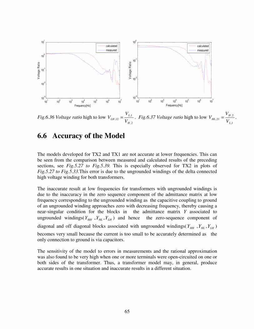
65
101
102
103
104
105
106
107
10-3
10-2
10-1
100
101
Frequency[Hz]
Vol
tage
Rat
io
calculatedmeasured
101
102
103
104
105
106
107
10-3
10-2
10-1
100
Frequency[Hz]
Vol
tage
Rat
io
calculatedmeasured
Fig.6.36 Voltage ratio high to low 2,
1,12,
H
LLH V
VV = . Fig.6.37 Voltage ratio high to low
1,
2,21,
L
HHL V
VV = .
6.6 Accuracy of the Model The models developed for TX2 and TX1 are not accurate at lower frequencies. This can be seen from the comparison between measured and calculated results of the preceding sections, see Fig.5.27 to Fig.5.39. This is especially observed for TX2 in plots of Fig.5.27 to Fig.5.33.This error is due to the ungrounded windings of the delta connected high voltage winding for both transformers. The inaccurate result at low frequencies for transformers with ungrounded windings is due to the inaccuracy in the zero sequence component of the admittance matrix at low frequency corresponding to the ungrounded winding as the capacitive coupling to ground of an ungrounded winding approaches zero with decreasing frequency, thereby causing a near-singular condition for the blocks in the admittance matrix Y associated to ungrounded windings( HHY , HLY , LHY ) and hence the zero-sequence component of
diagonal and off diagonal blocks associated with ungrounded windings( HHY , HLY , LHY )
becomes very small because the current is too small to be accurately determined as the only connection to ground is via capacitors. The sensitivity of the model to errors in measurements and the rational approximation was also found to be very high when one or more terminals were open-circuited on one or both sides of the transformer. Thus, a transformer model may, in general, produce accurate results in one situation and inaccurate results in a different situation.

66
6.7 Conclusion
This chapter demonstrated how a linear wide band frequency dependent model of a power transformer has been developed. A dedicated measurement setup to measure the admittance matrix over a wider frequency range has been designed. Vector fitting was adapted to subject the measured admittance matrix to rational function approximation. Network realization of the approximating rational function to its equivalent electrical network generated given in a Matlab generated file was used later to implement the model in a PSCAD script for time domain simulation. From the admittance matrix measurements taken at two different numbers of samples, the measurement setup was shown to give reproducible results. Comparison of results between measured, calculated and simulated results show good agreement. The model was however found to be sensitive to measurement errors especially for a transformer with ungrounded windings. The errors were magnified at lower frequencies and during open circuit conditions.

67
Chapter 7
CONCLUSIONS AND FUTURE WORK
7.1 Conclusions
In power systems that comprise an interconnection of cables, VCBs and transformers as in a wind farm, very severe high frequency overvoltages may occur due to the switching action of the VCB. Characterization of these overvoltages and the ultimate protection from them requires accurate modeling of the above components. The first part of this report dealt with cable modeling and experimental validations. It has been studied that the following conclusions can be drawn:
o With certain adjustments that take into account the semiconducting layers and core and sheath stranding, the Frequency Dependent (Phase) Model provided by PSCAD/EMTDC gives a fairly very good model of a real cable. This model replicates high frequency behaviors like skin effect, reflections, EM propagation.
o The results of the experiment show that good agreements have been achieved
between measured and simulated values in the frequency of oscillation and propagation delay. Small disagreements in these parameters are, however, noticed and the authors believe they can be due to unaccounted capacitance of the measuring cables and additional stray capacitances and inductances in the real system. Although it has been found that both simulations and measurements show an increase in damping of the EM transients with increasing frequency of oscillation as it should be, quicker damping is observed in reality than in the simulations.
VCB modeling and characterization of phenomena as current chopping, dielectric with stand and high frequency quenching capability makes the second part of this thesis. The following conclusions are inferred:
o The statistical nature of the arcing time, chopping current, dielectric strength, and quenching capability of a VCB requires that a stochastic model be developed for it.
o Although the VCB has good current interruption characteristics, its ability to
interrupt high frequency current zeros causes escalation of steep front

68
overvoltages on the load side due to reignitions or prestrikes specially when inductive currents are interrupted. This has been demonstrated by using a stochastic VCB model in a generic test circuit.
o The generic test circuit was able to replicate actual VCB characteristics and
expected results were obtained by looking into the effects of arcing time, rate of rise of dielectric strength, and high frequency quenching capability.
Finally, a wide band frequency dependent model of a power transformer was developed. This model is suitable for the study of transients induced due to VCB switching or other types which contain a very wide range of frequencies. The following points have been noted:
o Since the model is a linear black box equivalent based on measurements on the terminals as opposed to a detailed model of the internal parts of a transformer, it can only be used in transient studies involving overvoltages at the terminals, surge transfer and how it interacts with other external components during these events.
o The transformer model is a linear passive network equivalent of RLC elements.
Therefore, non linearity and core saturation of the transformers have not been accounted for. These characteristics are very pronounced for low frequency overvoltages. However, the model can work well for voltages significantly lower than the transformer rated voltage. In addition at relatively high frequencies where the core excitation flux varies very rapidly, these effects are small and can be neglected. Therefore, for high frequency transients, the model can be a sufficient representation.
o It has been tried to validate the model developed by studying voltage transfer
from the delta side to the wye side and vise versa. Although good agreements were obtained between voltage ratios calculated from the measured admittance matrix, simulated voltage ratios and those directly measured as function of frequency, there are discrepancies at lower frequencies. These errors are due to the ungrounded windings of the delta side which produces very small zero sequence components of elements associated with this winding at low frequencies.
7.2 Future Work A lot could be done to get an improved and more accurate model of the components especially the transformer.

69
Cable Model The cable model simulates most of the characteristics of a real cable and this was verified
to measurements on real cable. How ever the damping of the real cable was found to be higher than the PSCAD/EMTDC model besides the model doesn’t take in to account the presence of the armour. Hence more work could be done to get much more accurate model in this regard. VCB Model
The VCB model in this project simulates most of the phenomena of a real breaker very accurately and hence the authors feel it is good enough for its purpose. However a more accurate model can still be obtained by considering more aspects that were not dealt in this work. Transformer Model It was seen that the transformer model developed in this work is not accurate at lower frequencies; hence more work should be done to get a refined and robust model by taking in to account a lot of aspects that were not taken in to consideration on this work. The following is suggested:
Improving the measurement set up
The accuracy of this model depends on the accuracy of the measured admittance matrix and hence accurate measurement is required as the model is very sensitive to error in measurement.
One way to improve the accuracy of the measured data is by designing Special measurement setup dedicated to measure the admittance matrix and voltage ratio which allow easily reconnection and accurate measurement. One problem faced in this work was the measurement set up was so simple that it doesn’t allow easily reconnection. Reconnection has to be made every time a single element of the admittance matrix or voltage ratio was measured. For the three phase transformer with 36 admittance matrix and 9 voltage ratio elements for example 45 different connections was made. This was time consuming not mentioning its effect on the accuracy of the data set due to bad connection and inconsistency in the length of the connection cable used. This was reflected on the measurements obtained on the admittance and voltage ratio. Besides the simple connection cables used has greatly contributed to the measurement error. This was also seen during measurements where some elements of the admittance matrix and especially voltage ratio were very noisy. To deal with this problem the cables to be used in future work should be shielded.

70
Measuring the Zero sequence Admittance In accuracy of the model at lower frequencies for a transformer with ungrounded windings like the transformers we dealt with can be overcome by explicit measurement and modelling of the zero sequence system. Blocks of Y, which correspond to ungrounded windings ( LHHLHH YYY ,, ), are modified by removal of their zero sequence components as the zero sequence component of the admittance matrix is inaccurate due to small zero sequence current. A new zero sequence system has to be obtained by dedicated measurements and the two functions can then be approximated with rational functions which can be combined to produce the final model. In this work we have tried to measure the zero sequence admittance though we didn’t succeed to get accurate measurement.

71
REFERENCES
[1] D. Chapman, “The Cost of Poor Power Quality”, Power Quality Application Guide, Section 2.1, Copper Development Association of UK, November 2001. [2] Vic Smith, Venthanar Ilango, Sarath Perera, Vic Gosbell, Duane Robinson, “Transient Overvoltages On The Electricity Supply Network – Classification, causes and propagation,” Power Quality and Reliability Center, University of Wollongong. [3] A. Greenwood,”Electrical Transients in Power Systems”, 2nd Edition, Wiley-Interscience. [4] Pritindra chowdhuri, “Electromagnetic Transients in Power systems”, 2nd Edition. [5] D.J.Clare. “Failures of encapsulated transformers for converter winders at Oryx Mine”. Elektron magazine,March 1991, pp.24-27. [6] Van Craenenbroeck T, De Ceuster J, Marly J P, De Herdt H, Brouwers B, Van Dommelen D, 2000,"Experimental and Numerical Analysis of Fast Transient Phenomena in Distribution Transformers", Proc. IEEE/PES ,Winter Meeting, Singapore, CD-ROM (6P). [7] W. Sweet, _Danish wind turbines take unfortunate turn,_ Spectrum, IEEE, vol. 41,Issue 11, pp. 30-34, Nov. 2004. [8] J.Larssen, H.Soerensen, E.Christiansen, S. Naef, P.Völund “Experiences from Middelgrunden 40 MW Offshore Wind Farm,” Copenhagen Offshore Wind, 26-28 Oct. 2005. [9] B. Gustavsen, “Panel session on data for modeling system transients: Insulated Cables,” in Proc. IEEE Power Engineering Soc. Winter Meeting, 2001. [10] B. Gustavsen, J. A. Martinez, and D. Durbak, “Parameter Determination for System Transients- Part II: Insulated Cables,” IEEE Transactions on power delivery, vol. 20, no. 3, July 2005.
[11] PSCAD manual. [12] Janko KosmaE and Peter Zunko, “A Statistical Vacuum Circuit Breaker model for simulation of transient over voltages,” IEEE Transactions on Power Delivery, Vol. 10, No. 1, January 1995. [13] “Over voltages – Measurement and Statistical Simulation”, Industrial Group, TAVRIDA ELECTRIC.

72
[14] Mietek T. Gliiikowslti , hdoises R. Gutierrez and Dieter Brauii “Voltage escalation and re ignition behaviour of vacuum generator Circuit Breakers during Load Shedding,” IEEE Transactions on Power Delivery, Vol. 12, No. 1, January 1997. [15] M. Popov, L. van der Sluis “Comparison of two vacuum circuit breaker arc models for small Inductive Current Switching,” [16] Helmer J., Lindmayer M. “Mathematical Modeling of the High Frequency Behaviour of Vacuum Interrupters and Comparison with measured transients in power systems,” XVIIth International Symposium on Discharges and Electrical Insulation in vacuum, Berkley, USA, 1996. [17] B. Kondala Rao, and Gopal Gajjar,”Development and Application of Vacuum Circuit Breaker Model in Electromagnetic Transient Simulation,” IEEE Transactions on Power Delivery 2006. [18] R P P Smeets, “Stability of low-current vacuum arcs,” J. Phys. D: Appl. Phys.1 9 (1986) 575-587. Printed in Great Britain. [19] S.M. Wong, L.A. Snider and E.W.C. Lo, “Over voltages and Reignition behaviour of Vacuum Circuit Breaker”, International Conference on Power System Transients – IPST 2003. [20] S. Giere, H. C. Kärner, H. Knobloch, switching capability of double and single- break vacuum interrupters – experiments on real high highvoltage demonstration-tubes, Technical University of Braunschweig, Germany. [21] Marjan Popov, Lou van der Sluis, Gerardus C. Paap,and Hans De Herdt “Computation of Very Fast Transient Overvoltages in Transformer Windings”, IEEE TRANSACTIONS ON POWER DELIVERY, VOL. 18, NO. 4, OCTOBER 2003. [22] A. Morched (SM), L. Mad (M), J. Ottevangers” A High Frequency Transformer Model for the EMTP”, IEEE Transactions on Power Delivery. Vol. 8, No. 3. July 1993. [23] Bjørn Gustavsen ,”Wide Band Modeling of Power Transformers”, IEEE TRANSACTIONS ON POWER DELIVERY, VOL. 19, NO. 1, JANUARY 2004. [24] B. Gustavsen and A. Semlyen, "Rational approximation of frequency domain responses by Vector Fitting", IEEE Trans. Power Delivery, vol. 14, no. 3, July 1999, pp. 1052-1061. [25] B. Gustavsen,” Rational approximation of frequency dependent admittance Matrices", IEEE Trans. PWRD, vol. 17, no. 4, Oct. 2002, 1093-1098. [26] http://www.energy.sintef.no/produkt/VECTFIT/index.asp

73
[27] B. Gustavsen, “Rational approximation of frequency domain responses by vector fitting”, IEEE Transactions on power delivery, Vol. 14, No.3, July 1999. [28] B.Gustavsen,”Enforcing Passivity for Admittance Matrices Approximated by Rational Functions”, IEEE transactions on power systems,vol.16, No. 1,February 2001.
[29] Stefano Grivet-Talocia, “ Passivity enforcement via perturbation of Hamiltonian Matrices”, E transactions on circuits and systems—I: regular papers, vol. 51, no. 9, september 2004. [30] Maialen Boyra,” Transient Overvoltages in Cable Systems”, Master of Science Thesis, Göteborg, Sweden, 2007. [31] Daniel Mireanu, ” Transient Overvoltages in Cable Systems”, Master of Science Thesis, Göteborg, Sweden, 2007.

74
APPENDICES
Appendix A. Implementation of 3-phase Transformer model in PSCAD/EMTDC In this appendix the procedure for implementing the transformer model developed in this thesis in transient time simulation software PSCAD/EMTDC is demonstrated. The out put of the main Matlab source code is either a state space equivalent or a file of branch cards of an equivalent RLC network of the transformer. The later can be used directly in PSCAD/EMTDC or other time simulation packages to build the transformer component. A branch based interface was used to define the branches of the equivalent network. Branch design is accomplished by specifying the type and size of passive elements (i.e. lumped R, L and/or C), and to which electrical connections they fall between. The component definition is written as a script in the format $<TO> $<FROM> [<R>] [<L>] [<C>] where $<TO> and $<FROM> refer to the branch end nodes and [<R>] , [<L>] , [<C>] to the passive element values in Ohm, Henry and micro Farad respectively. Nested page modules are used to build the model as the number of branches is too big to implement as a single component. Therefore each one of the big branches between two nodes or between a node and ground is modeled as sub modules which are then connected to form the whole network. The steps are summarized as follows: 1. Create a new component page module in the circuit page with 3 connections on the left, 3 on the right and one at the bottom, ground to model the whole equivalent network as in Fig. A.1. 2. Double click on the newly created page module and create components corresponding to each one of the big branches. Connect these blocks between corresponding nodes (connections) referred in 1 as shown in Fig. A.2.

75
Fig. A.1 Transformer component page module. 3. Enter component definitions for each one of the components in 2 as script. A typical script page would look like as in Fig. A.3.

76
Fig. A.2 Components corresponding to internode branches.

77
Fig. A.3 Component definition as script page.

78
Appendix B. Network Realization Consider the multi-terminal network shown in Fig.B.1 the admittance matrix for this network can be computed as A diagonal element iiY of the admittance matrix is obtained as the sum of admittances for all branches connected to terminal i, including branches to ground,i.e.,
�≠=
+=n
ijjijiii yyY
,1 (1)
The off-diagonal elements are the negative of the admittances connecting buses i and j i.e., ijij yY −= (2) Where iy denotes the admittance of a branch connected between terminal i to ground and
ijy admittance connected between terminal i and j. Given the admittance matrix we can also compute the admittance of the branches connected between terminals and a terminal to ground. From (2) the admittance of the branch connected between terminal i and j may be written as ijij Yy −= (3) Similarly the branch between terminal i to ground can be computed from (1)
�
≠=
−=n
ijjijiii yYy
,1
(4) If the value of ijy from (2) is replaced in to (4) then
�≠=
+=n
ijjijiii YYy
,1
(5)
We may write (5) in compact form according to:
�=
=n
jiji Yy
1
(6)

79
Given the admittance matrix of a device in frequency domain the corresponding network can easily be obtained connecting branches between terminals and terminal to ground by realizing the admittances obtained from (3) and (6). This gives a network of the form shown in Fig.B.1. Fig.B.1 Multi- terminal network equivalent of a device. Fundamentals of Network Synthesis A network is represented by a rational function in s-domain. This rational function is called network function. Network functions are expressed in terms of the complex frequency variable s, resulting from the application of Laplace transformation to time domain network equations. This network functions are either impedance or admittance. Given the impedance or admittance function then it possible to find the network representation. As a passive net work is an inter connection of the basic passive elements; resistor, capacitor, and inductor; let’s start by driving the network function of this elements which is the basic for synthesis of a complex network including the network we are trying to find for the transformer model. The voltage and current at the terminals of these elements in time domain t and frequency domain s is given in Table B.1 is given by
1y
ny2y
12y21
nny 2ny1

80
Table B.1 Voltage and current relation ship of passive elements RESISTOR CAPACITOR INDUCTOR Relation ship between voltage and current in time domain
)()()()(
tGvti
tRitv
==
dt
tdvCti
vdxxiC
tvt
)()(
)0()(1
)(0
=
+= �−
�−+=
=
t
idttvL
ti
dttdi
Ltv
0
)0()(1
)(
)()(
Relation ship between voltage and current in frequency domain
)()(
)()(
SGVSI
SRISV
==
)]0()([)(
)0()(
1)(
−
−
−=
+=
vSSVCSIS
vSI
SCsV
Si
SVSL
sI
iSSILSV
)0()(
1)(
)]0()([)(−
−
+=
−=
The impedance and admittance functions are defined as the ratio of voltage to current transform and current to voltage transformer.
)()(
)(SISV
SZ = (7)
)()(
)(SVSI
SY = (8)
If the initial conditions in Table.B.1 are zero then the impedance and admittance functions of the elements can easily be computed (7) and (8). Table B.2 Network function of the basic elements RESISTOR CAPACITOR INDUCTOR Impedance Z(S)
RSISV
SZ ==)()(
)(
CSSISV
SZ1
)()(
)( == LS
SISV
SZ ==)()(
)(
Admittance Y(S) G
SVSI
SY ==)()(
)( CSSVSI
SY ==)()(
)( LSSV
SISY
1)()(
)( ==
Suppose Y(s) represent the admittance function of one of the branches of n-terminal network representation of the Fig.B.1 and assume that it can be written in partial fraction expansion of the form
� ++−
=N
eSdaS
rSY
1
.)( (9)
esdjaas
jrrjaas
jrrjaas
jrrjaas
jrras
rsY ....
)"("'
)"'("'
)"'("'
)"'("'
)(22
22
22
22
11
11
11
11 ++++−
++
−−−
++−
++
−−−
+−
= (10)

81
esdaaSas
ararSr
aaSas
ararSras
rsY ....
"''2""2''2'2
"''2""2''2'2
)(2
22
222
222222
12
112
11111 +++++−
−−+
++−−−
+−
= (11)
The network function in (11) can be realized in to its corresponding network. Each part represent admittance of an element or combination of elements and the final network can be obtained by connecting these branches in parallel as admittance in parallel sum up. We can further simplify (12) by .....)()()()()()( 54321 +++++= SYSYSYSYSYSY (12) where dsY =)(1 eSSY .)(2 =
aS
rSY
−=)(3
Now let’s realize each section starting from the simplest )(1 sY From Table.B.1
dsY =)(1 ,represents admittance of a resistor with a resistance value of d
R1=
SeSY .)(2 = ,represents admittance of a capacitor with a capacitance value of eC =
One can write )(3 SY as
)(1
11
)(3
3 SZra
Sr
SY =−
= , where ra
Sr
SZ −= 1)(3 is an impedance function representing
a series combination of an inductor with an inductance value of r
L1= and a resistor with
a resistance value of ra
R−= as impedances in series sum up.
)'''
1(''
)''''2''2
)'''
1(''
'21
'2'
'2''''
.21
1"''2
""2''2'2)(
21
212
111
21
212
11
12
11
21
211
211111
4
rr
a
ararS
rr
a
rra
rra
Sr
aaSasararSr
SY
+
−−
+
+−+=
++−−−
= (13)
The above equation can be written as

82
)()(1
)(54
4 SZSZSY
+=
)(4 SZ and )(5 SZ are in series and each can be realized as follows
)(4 SZ is a series combination of an inductor with a resistor whose values can be
computed as follows
'2'
'2''''
.21
)(1
12
114 r
arra
Sr
SZ −+= (14)
(14) can be written as:
RLSSZ +=)(4 (15) Equating (14) and (15) gives the values of L and R as
121r
L = ,'2'
'2''''
1
12
1 ra
rra
R −=
)'''
1(''
)''''2''2
)'''
1(''
'21
)(
21
212
111
21
212
15
rr
a
ararS
rr
a
rSZ
+
−−
+
= (16)
Similarly if (16) is rearranged as
GCSSZ
+= 1
)(5 (17)
Then )(5 SZ can be realized as a parallel combination of a capacitor and a resistor whose values can be computed by equating (16) and (17).
)
'''
1(''
'2
21
212
1
rr
a
rC
+= ,
)'''
1(''
)''''2''2
21
212
111
rr
a
ararG
+
−−=
The final network will then look like:

83
Fig.B.2 Network realization of Y(s).
...0R 0C
rR
rL
cR
cL
cCcG
...
Constant term s.e term Real Pole Complex conjugate pole