Analysis of the Design Variables of Thermoforming Process on … · 2018-10-18 · Thermoforming is...
28
Analysis of the Design Variables of Thermoforming Process on the Performance of Printed Electronic Traces Gill M., Gruner A.*, Ghalib N., Sussman M., Avuthu S., Wable G, Richstein J. Jabil St Petersburg, Florida, *Vienna, Austria Abstract One specific market space of interest to emerging printed electronics is In Mold Label (IML) technology. IML is used in many consumer products and white good applications. When combined with electronics, the In Mold Electronics (IME) adds compelling new product functionality. Many of these products have multi-dimensional features and therefore require thermoforming processes in order to prepare the labels before they are in-molded. While thermoforming is not a novel technique for IML, the addition of printed electronic functional traces is not well documented. There is little or no published work on printed circuit performance and design interactions in the thermoforming process that could inform improved IME product designs. A general full factorial Design of Experiments (DOE) was used to analyze the electrical performance of the conductive silver ink trace/polycarbonate substrate system. Variables of interest include trace width, height of draw, and radii of both top and bottom curvatures in the draw area. Thermoforming tooling inserts were fabricated for eight treatment combinations of these variables. Each sample has one control and two formed strips. Electrical measurements were taken of the printed traces on the polymer sheets pre- and post- forming with a custom fixture to evaluate the effect on resistance. The design parameters found to be significant were draw height and bottom radius, with increased draw and smaller bottom curvature radii both contributing to the circuits’ resistance degradation. Over the ranges evaluated, the top curvature radii had no effect on circuit resistance. Interactions were present, demonstrating that circuit and thermoforming design parameters need to be studied as a system. While significant insight impacting product development was captured further work will be executed to evaluate different ink and substrate material sets, process variables, and their role in IME. Introduction Printed electronic technology is an additive printing process that creates an electronic circuit by depositing one or several layers of conductive ink onto a substrate. Substrate choices include conformable and stretchable plastic films. Additional functional inks may be printed on the circuits for passive and active components like resistors, insulators, and for protection of the circuit in end-use applications. The printed circuitry is application-dependent and may vary from simple passive to complex multi-layer structures. In-mold printed electronics is an emerging technology extending the integration possibilities of electronics into applications that have historically not been possible with traditional printed circuit board technology. Thermoforming is a process utilizing heat and either vacuum or high gas pressure to form a softened thermoplastic film onto a mandrel of desired shape and size (Figure 1) [1]. The film is placed on the tooling plate, transported into the chamber that is then heated. The vacuum or gas pressure pushes the softened film down onto the tooling insert to take the shape. Though it is a widely used technology in forming thermoplastics for packaging, white goods, and consumer products, the integration of printed electronics into the thermoforming process is relatively recent. The impact of the thermoforming process on the performance and limitations of printed electronics circuitry and the respective product and process design guidelines are not fully understood. Figure 1 Schematic of a thermoforming process (left) and tooling plate (right)
Transcript of Analysis of the Design Variables of Thermoforming Process on … · 2018-10-18 · Thermoforming is...
Analysis of the Design Variables of Thermoforming Process on the Performance of
Printed Electronic Traces
Gill M., Gruner A.*, Ghalib N., Sussman M., Avuthu S., Wable G, Richstein J.
Jabil
St Petersburg, Florida, *Vienna, Austria
Abstract
One specific market space of interest to emerging printed electronics is In Mold Label (IML) technology. IML is used in
many consumer products and white good applications. When combined with electronics, the In Mold Electronics (IME) adds
compelling new product functionality. Many of these products have multi-dimensional features and therefore require
thermoforming processes in order to prepare the labels before they are in-molded. While thermoforming is not a novel
technique for IML, the addition of printed electronic functional traces is not well documented. There is little or no published
work on printed circuit performance and design interactions in the thermoforming process that could inform improved IME
product designs. A general full factorial Design of Experiments (DOE) was used to analyze the electrical performance of the
conductive silver ink trace/polycarbonate substrate system. Variables of interest include trace width, height of draw, and
radii of both top and bottom curvatures in the draw area. Thermoforming tooling inserts were fabricated for eight treatment
combinations of these variables. Each sample has one control and two formed strips. Electrical measurements were taken of
the printed traces on the polymer sheets pre- and post- forming with a custom fixture to evaluate the effect on resistance. The
design parameters found to be significant were draw height and bottom radius, with increased draw and smaller bottom
curvature radii both contributing to the circuits’ resistance degradation. Over the ranges evaluated, the top curvature radii
had no effect on circuit resistance. Interactions were present, demonstrating that circuit and thermoforming design
parameters need to be studied as a system. While significant insight impacting product development was captured further
work will be executed to evaluate different ink and substrate material sets, process variables, and their role in IME.
Introduction
Printed electronic technology is an additive printing process that creates an electronic circuit by depositing one or several
layers of conductive ink onto a substrate. Substrate choices include conformable and stretchable plastic films. Additional
functional inks may be printed on the circuits for passive and active components like resistors, insulators, and for protection
of the circuit in end-use applications. The printed circuitry is application-dependent and may vary from simple passive to
complex multi-layer structures. In-mold printed electronics is an emerging technology extending the integration possibilities
of electronics into applications that have historically not been possible with traditional printed circuit board technology.
Thermoforming is a process utilizing heat and either vacuum or high gas pressure to form a softened thermoplastic film onto
a mandrel of desired shape and size (Figure 1) [1]. The film is placed on the tooling plate, transported into the chamber that
is then heated. The vacuum or gas pressure pushes the softened film down onto the tooling insert to take the shape. Though
it is a widely used technology in forming thermoplastics for packaging, white goods, and consumer products, the integration
of printed electronics into the thermoforming process is relatively recent. The impact of the thermoforming process on the
performance and limitations of printed electronics circuitry and the respective product and process design guidelines are not
fully understood.
Figure 1 Schematic of a thermoforming process (left) and tooling plate (right)

The forming process moves substrate material and creates high stress areas within the substrate as it is forced to conform to
the mandrel, potentially having adverse effects on printed trace performance and mechanical integrity (Figure 2). As the
substrate and ink deforms conductive particles separate and compress impacting the conductivity. This change may be
significant in some areas where discontinuity may lead to partial connectivity or catastrophic failure. This study focuses on
three of the most likely mandrel design parameters that might adversely affect circuit performance: depth of draw (height),
top radius (Rt), and bottom radius (Rb) (Figure 3 & 4). The experimental design was completed by evaluating the effect on
printed electronic traces of five different widths over replaceable mandrel inserts in a thermoforming tool.
The results of these studies will provide the product designer with initial guidelines on how to compensate for anticipated
electric conductivity degradation from thermoforming, minimizing costly prototyping and design iterations. Conceptually,
the designer will eventually have access to a complete matrix of all needed information for electronic circuit design, suitable
material sets, electronic trace geometry/conductivity relationships, and mechanical properties, within acceptable
thermoforming limits.
Evaluating these thermoformed traces raises some interesting challenges and opportunities as there are major differences
between thermoformed printed electronic traces and traditional Cu based PCBA electronic traces. There are a few
assumptions that have to be made when evaluating these samples. When a product is thermoformed, the material does not
have equal amount of draw and strain induced along the entire length of a trace. Inspections to investigate changes along the
cross-sectional area are challenging to calculate along the entire trace. It is very difficult to measure the dimensional changes
of the printed traces in all three dimensions, assuming no other performance impacting factors such as pin holes of polymer
or varying conductive particle distribution in a printed trace. Particles need to be in contact together for current to flow, but
this is not a bulk copper wire, where it is acceptable to assume a solid cross sectional area. In printed electronics, it is known
that the “solids” part of the trace is actually more porous with a nonconductive polymer binding making up part of the trace
(Figure 5) [2]. Other contributing factors not investigated here are the polymer structure from raw material processing,
different molecular structures of ink and substrate processing methods varying from supplier to supplier, and differing elastic
properties of the materials. For example, within a material, an amorphous versus crystalline structure may create areas with
different internal stresses that can affect how the material is drawn during thermoforming. Different functional inks have
different solids loading, particle shapes, and particle sizes, with varying distributions. This may be impacted by the
homogeneity of the ink system due to mixing. These could have implications on how well the ink can conduct electrically
before and after forming.
Figure 5 Conductive particles of different shapes and sizes distributed in a printed trace. Left image shows high
porosity, less surface contact between particles resulting in a higher resistance trace. Right image shows a higher
packing density trace closer to traditional solid PCB trace with lower resistance
Figure 4 Design parameters studied on the test vehicle Figure 3 Thermoformed test vehicle
Figure 2 Simulation of the thermoformed test vehicle

Discussion of Methodology
The test vehicle contained three strips of eight parallel electronic traces per sample. Each trace had a different width, ranging
from 5700 µm down to 150 µm (Figure 6). The basic relationship of electric resistance as function of trace width should be
an inverse parabolic curve. Since resistance is an inverse proportion to area, but the lengths are the same, those values cannot
be compared directly in our test vehicle. A goal was to establish a lower trace width limit for which the trace could reliably
be printed with the selected material set and screen. Consistent quality of formed prints was obtained down to 1700 µm,
yielding five trace widths for inclusion in the experiment. The replaceable mandrel portion of the DOE was a full factorial,
including three variables at two levels of the height, Rt, and Rb (Table 1). Eight different inserts were required to complete
the study. With the inclusion of the five trace widths, the general full factorial experiment consisted of 40 trials. All printing,
drying and forming parameters were held constant. A custom substrate test fixture with tooling holes allowed probing the
traces in a consistent location (Figure 7). A programmable 6.5 digit multi-meter was used to collect trace resistance data.
Each trace from all of the samples was measured three separate times, resulting in 600 data points.
Understanding the impact of key thermoforming process variables on electrical properties can help designers to select an
appropriate trace width for a given geometric shape of a (to be) formed product. How the forming process affects the trace’s
cross-sectional area, particle distribution, packing density, and the mechanical integrity of the trace, will directly impact the
electrical performance, and may gate product design. With forms and designs of thermoformed products that are more
complex, multiple trace segments will change electrical performance of the electrical circuit.
Table 1 Design of experiments (DOE) factors, number of levels, and parameters
Factor Number of Levels Level Parameters Trace width 5 X, X+1, X+2, X+3, X+4
Height 2 H, H+1 Top Radius 2 T, T+1
Bottom Radius 2 B, B+1
Figure 6 Test vehicle screen (left) and printed (right)
Figure 7 Custom electrical test fixture for resistance measurements

Results
Resistance measurements were taken pre and post forming to assess resistance changes introduced by the thermoforming
process. The significant DOE factors were height, bottom radius and trace width, while the top radius was found not to be
significant. The Rsq for the model of the analysis was 96.76 percent, adjusted Rsq is 96.58 percent, and predicted Rsq is 96.36
percent Table 2 in Appendix. Residual plots are also included for reference in Appendix (Figure 14).
The factorial plot depicts the significance of height, bottom radius, and trace width on the formed electrical traces (Figure 8).
The top radius as a main factor had no impact. The shape of the curve for trace width is of parabolic type.
Normalizing resistance on the assumption the traces have constant resistivity and length and A (area) is w*h
• (w = width, h = height)
• ; solving for h using the means of the plots: average height parameter
for all traces.
• The value of h is not assumed equivalent to the physical observable height-- it shows a consistent ink
deposition.
An Analysis of Variance (ANOVA) was conducted separately per each trace width to ensure all trends for each trace were
the same as the overall model. The mean trace resistance with increased forming height was 2.5 Ω, the top forming radius had a negligible impact, and bottom forming radius had a strong impact by decreasing mean trace resistance by 1.5Ω (Figure 9).
The slope differences in the plots indicate design interactions between height and bottom radius, height and trace width, and
top radius and bottom radius (Figure 10 & 11). The factors that did not interact are top radius - trace width and top radius –
height.
Figure 8 DOE factorial plot of post-formed mean resistance (Ω) for the full design
Figure 9 DOE factorial plot of post-formed mean resistance (Ω) for X+4 mm trace width

Discussion
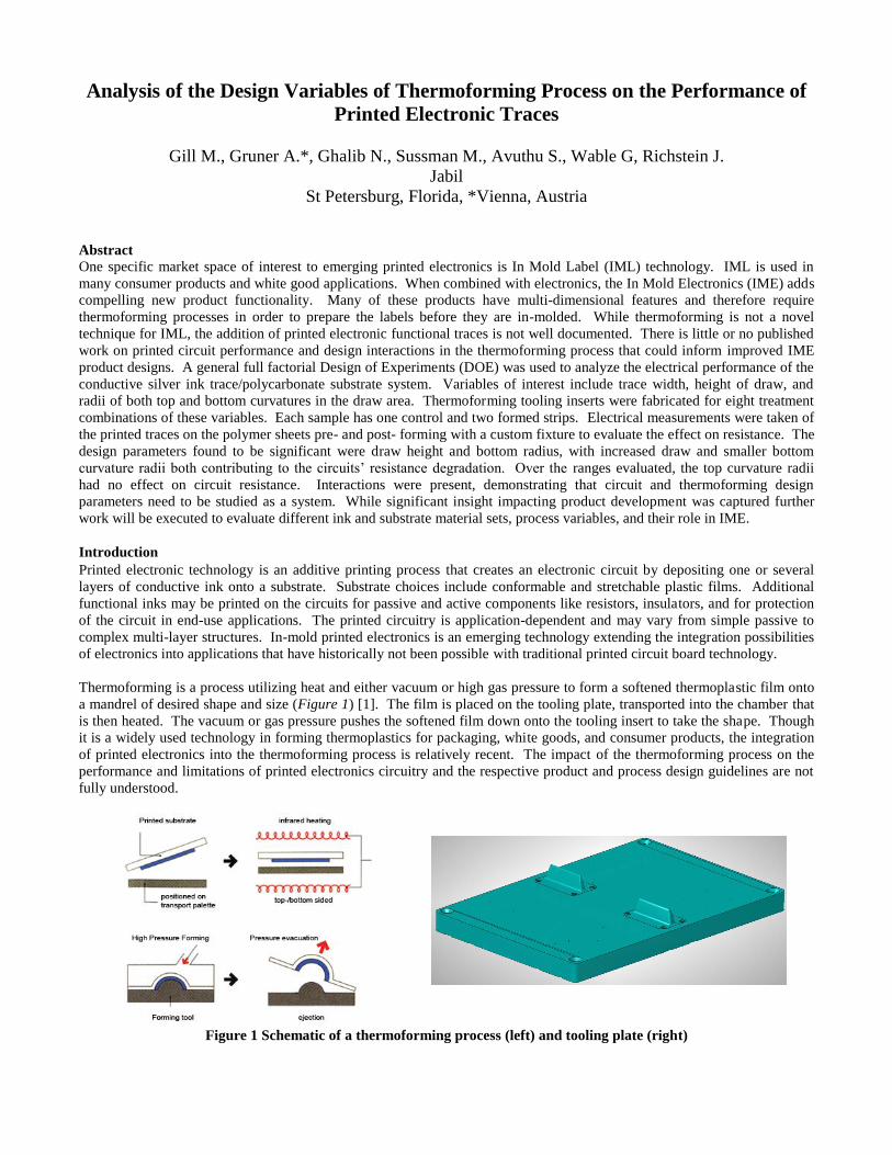
In thermoforming, the stress concentrators within the draw region vary depending on some of these dominant geometric
variables (Figure 12). The larger top radii limit material movement that can be shared along the flank of the draw during the
forming process, resulting in a thinner wall thickness. Paired with a smaller bottom radius, which requires a deeper draw
length the material is thinned further (Figure 13). This may increase trace cracking potential leading to a reduced or even
catastrophic failure in electrical performance. The larger the required draw height required to meet the design of a product,
the more susceptible the traces will become to these described failure. Electrical conductivity of the printed trace is subject to
Large Bottom Radius Small Bottom Radius
Small
Top
Radius
Large
Top
Radius
Figure 12 Quadrant figure of four varying cross-sectional sketch of the thermoformed parts
Figure 10 & 11 Interaction Plots for post-formed mean resistance (Ω) (left) full factorial DOE (right) for X+4 mm
trace
Figure 13 Overlay of forms of varying bottom
radius, the bigger bottom radius undergoes less
elongation

counteracting mechanisms. The net effect will determine electrical conductivity. The negative effect of elongation due to
particle separation can be offset by compression due to pressure and heat that increases contact between particles.
Conclusions
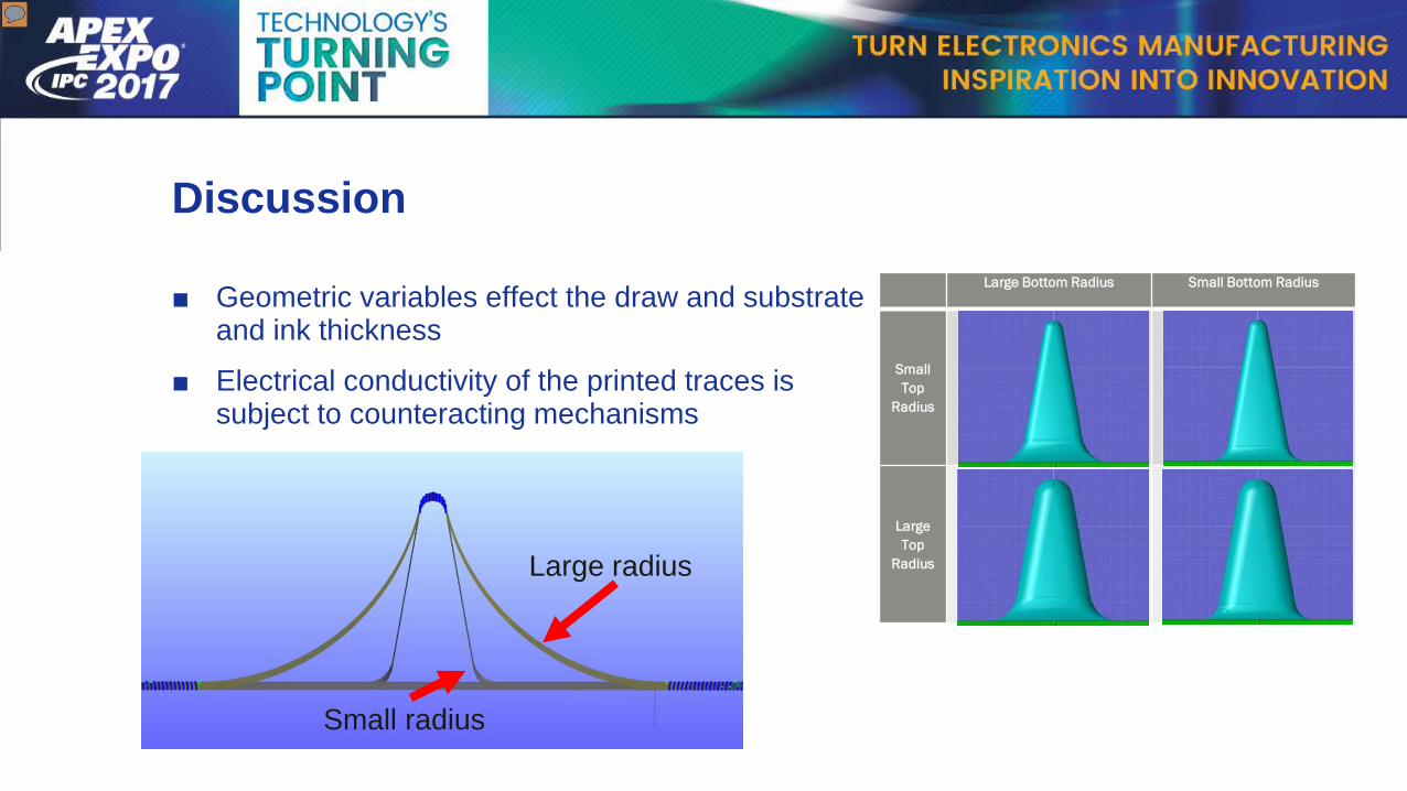
As expected, there is a parabolic mean variation of resistance as a function of trace width. This study did not consider
variability and shape of the ink deposit, which could introduce other variance.
The wider the traces, the less the draw height impacts the electrical performance.
The sharper the bottom radius, the more stress is induced with an increased probability of trace discontinuities.
The top radius did not have an impact on the resistance changes after forming in the range studied as a main factor.
There were numerous design interactions between the design variables. At the lower draw height, the radius did not have an
effect. However, as the draw height increased, it caused a large difference in resistance. This translates into product design
and electrical operating limits.
This study covered a limited range of varying radii, however, additional levels in these factors will be included in later
studies. Future investigations will address interactions in more detail to determine potential design trade-offs for product
design and functionality.
Summary
This experiment provides insight into future design guidelines and process intellectual property (IP) for manufacturing
printed electronic products. The design was a 40 trial experiment, investigating the effects of various design variables draw
heights, curvatures, and printed trace widths. The observations and data of this full factorial DOE suggest there are multiple
interactions of parameters. The main interaction appears to be the bottom curvature radius and the amount of draw that
impact the electrical performance. Height and trace width, height and top radius also contribute significant p-values
according to the ANOVA table. Complimentary work analyzing grid patterns deformation is being done. Future work will
include different design windows and explore additional material sets in greater depth.
Acknowledgments
A special thank you to Doug Greenfield for his mentorship and guidance throughout the analysis of the research.
We would like to thank other noteworthy contributors, George Oxx and Gina Clifford, for their valuable time and efforts
providing feedback.
We thank our appreciated intern Nicholas Conde for his assistance collecting hundreds of data points for the analysis.
Reference
[1] Niebling Form Technologie. C12.06.2009. Federal Republic of Germany: Niebling Form Technologie; [accessed 2016
Jun 6]. http://www.niebling-form.com/en/high-pressure-thermoforming/
[2] Banfield, D. 2000. Understanding and Measuring Electrical Resistivity in Conductive Ink and Adhesives. SGIA Journal
(June 2000 Edition). [Accessed 2016 Sep 27]. http://www.conductivecompounds.com/pdf/sgia.pdf
Appendix

Table 2 ANOVA Table
Figure 14 Residual plots for the full factorial DOE

Analysis of Thermoforming Design Variables on the Performance of Printed Electronics
MaryAlice GillJabil

Product development
Process development
Technology development
Adaptation of Electronics
[1]
Presenter
Presentation Notes
The theme of APEX is electronics (& innovation) and we’ve heard a little bit about printed electronics technology at this point. We all know that technology is rapidly changing.. The demand for a new kind of product is huge. And that translates to a lot of pressure with these new requirements for manufacturers. A lot of novel approaches are being undertaken, new materials, new process, the merging of existing technologies that have never been done. So here we are doing research as manufactures to really bring this innovation to life. Because we want to be here…we want to be leading the pack to build and release new products.

Outline
Technology Overview
Goal
Design of Experiments (DOE)
Results
Discussion
Presenter
Presentation Notes
The technology overview, some general background info for those that might not be familiar. The goal because of course that’s really important, what's a study for without a scope, right? The design of the experiments, here I’ll introduce the test vehicle, parameters and testing. And the heart of all things important for a research study the results, discussion, conclusion, and summary. Let’s be honest no one cares about those bullet points, we all know the flow of a presentation…this is just here to entice you about the research with an interesting picture of the test vehicle.

In Mold Label (IML)
Various products & markets
Increased durability
No further processing
[3] [4]
[2]
Presenter
Presentation Notes
So as I said before we’ve got a merging of technologies coming about…so let’s take it far from electronics right now… Packaging, labels…plastics. Taking regular plastic thermoformed parts and imbedding the labels into the packaging to streamline the process. Making the labels of these containers more durable across many different market spaces. In mold labeling is a technology that has been around for a long time. It’s a way of creating a robust, in line solution to making many of our everyday products. This is not a new development by any means. But, here comes the novelty….

In Mold Electronics (IME)
Market demand
Consumer goods Industrial/Commercial applications Aerospace/Automotive
Integration of printed electronics
Light weight Flexible In line manufacturing
Consumer goods
In line IME equipment
Presenter
Presentation Notes
In Mold electronics commonly known as IME. The market and consumer shift for a different product drives the need for this new/ merging of technologies. So now we’re seeing a lot of work and money being put into feasibility of integrating electronics with plastics, by using various forms of printed techniques, otherwise known as printed electronics. We want/need lighter weight, flexible, basically more diverse and functional properties in our products.

Transitioning to (IME)
Removing design constraints
Adding functionality + value
Enables new products
Presenter
Presentation Notes
This transition into IME is happening to remove some constraints in form factor and adds electronic functionality to products. Which increases value of products. It is also allowing the creation of products that have only been dreamed about. Adding printed electronic to create functional labels. These don’t just showcase graphics, but add value to the part. Production can be faster, parts can be lighter. Printed electronics is an additive process using conductive inks deposited onto a flexible substrate. Printed electronic technology is an additive printing process that creates an electronic circuit by depositing one or several layers of conductive ink onto a substrate. Substrate choices include conformable and stretchable plastic films. Additional functional inks may be printed on the circuits for passive and active components like resistors, insulators, and for protection of the circuit in end-use applications. The printed circuitry is application-dependent and may vary from simple passive to complex multi-layer structures. In-mold printed electronics is an emerging technology extending the integration possibilities of electronics into applications that have historically not been possible with traditional printed circuit board technology.

Thermoforming Overview
[6]
[5]
Presenter
Presentation Notes
Let’s talk a little bit about the thermoforming process and why it is really important to understand various parameters. Basically, thermoforming utilizes heat and either vacuum or high pressure to soften a thermoplastic film on a mandrel of desired shape and size (Figure 1) [1]. The film is placed on the tooling plate, and moves into a heated chamber. The vacuum or gas pressure pushes the film onto the tooling insert to create the desired form. Though it is a widely used technology in forming thermoplastics for packaging, white goods, and consumer products, the integration of printed electronics into the thermoforming process is relatively recent. The impact of the thermoforming process on printed electronics circuitry’s performance (mechanical and electrical) and any limitations for product and process is unknown.

Goal
Develop design guidelines
Comparing printed traces to copper
Quantify traces for specific applications
Presenter
Presentation Notes
So our goal as manufacturers is to uncover these unknowns. The results of these studies will provide the product designer with initial guidelines on how to compensate for anticipated electric conductivity degradation from thermoforming, minimizing costly prototyping and design iterations. Copper wire has been and can be safely assumed to be a solid.

Simulation of thermoformed test vehicle
Design of Experiments (DOE)Factor Number of Levels Level Parameters
Trace width 5 X, X+1, X+2, X+3, X+4
Height 2 H, H+1
Top Radius (Rt) 2 T, T+1
Bottom Radius (Rb) 2 B, B+1
Presenter
Presentation Notes
The DOE was laid out to evaluate some of the design parameters trace width, Height, the top and bottom radius that would have a major impact on traditional thermoformed parts. Analyzing the traces with respect to these factors uncovers the functional impact on electrical performance that for traditional products doesn’t matter, since as long the product can hold up, doesn’t break/fracture during shipment and use, it’s good. As the substrate and ink deforms conductive particles separate and compress impacting the conductivity. This change may be significant in some areas where discontinuity may lead to partial connectivity or catastrophic failure. We may not be able to uncover the specific particle phenomena on a molecular/micro level, but on a functional level we can understand and quantify the effects.

Test Vehicle
Presenter
Presentation Notes
In the test vehicles, a control was left “unformed” to look at the baseline comparison of the effects of the thermoforming process without the design considerations. Resistance measurements Custom fixture for repeatability

ANOVA
Presenter
Presentation Notes
First off – I’m sorry for this eye sore of a slide, not trying to go for “death by power point”. I know you’re all hungry and ready to eat. But this is exciting results (well let me just speak for myself)…not sure how you feel about it hahaha, hopefully you think it’s interesting! Resistance measurements were taken pre and post forming to assess resistance changes introduced by the thermoforming process alone. There was an effect, according to our data that shows a decrease in the resistance. At this time, we didn’t do a deep dive into this effect, it is something we will be looking into in a later study. Looking at the ANOVA table (I’m sure most of you know, but in case you don’t, it is an analysis of variance table which evaluates the data to compare hypothesis against the population mean). So we can see that the F and p- values show that a few of our factors stand out as significant parameters on the measurements - height, bottom radius and trace width. Trace width doesn’t have any statistical significance. I will explain a little deeper later on why we believe this is happening. The model which brings validity to the data is shown by these Rsqvalues 96.76 percent, adjusted Rsq is 96.58 percent, and predicted Rsqis 96.36 percent. Residual plots are also included for reference of error and distribution of the data, it shows that the data has a good distribution.

Presenter
Presentation Notes
Now we can look at the significance in the means of the factors visually. The top radius there’s no slope, no change, basically no effect. The shape of the curve for trace width is of parabolic. It as expected, the thinner traces have a smaller cross-sectional area increasing resistance. The value of h is not assumed equivalent to the physical observable height– with some quick math it shows a consistent ink deposition. By normalizing resistance on the assumption the traces have constant resistivity and length and A (area) is w*h (w = width, h = height) 𝑅= 𝜌 𝐿 𝐴 ∝ 1 𝑤∗ℎ ; solving for h using the means of the plots: ℎ∝ 1 𝑤∗𝑅 ≈0.02 average height parameter for all traces.

H+1H
10.0
9.8
9.6
9.4
9.2
9.0
T+1T B+1B
HeightM
ean
of F
orm
ed R
esist
ance
Top Radius Bottom Radius
Factorial Plot Formed Resistance for X+4 TraceFitted Means
All displayed terms are in the model.
Presenter
Presentation Notes
To see the significance of the height and bottom radius results better, I ran the analysis again, looking at only one trace width. It also validated that the trends were a consistent fit to the overall model. Here we are looking at the mean resistance for the widest trace. Height has the biggest effect at a difference of 2.5 Ω, the sharper/smaller the bottom radius the resistance increased about 0.6/0.7 Ω. And top radius changed 0.3ish Ω.

Presenter
Presentation Notes
Here the big take away is that there’s no interaction between the top radius/height and the top radius/width. And the largest interaction is height/bottom radius, with some mild interaction with the other factors. For the trace width interactions, the there’s less slope change for the wider traces than the smaller traces, indicating that the more ink deposited the less susceptible the traces are to lower conductivity impacts.

Presenter
Presentation Notes
Again looking at just the one trace width, things get a little easier to look at and we’ve seen that the width does matter, and the interaction of height and top radius doesn’t.
Discussion
Geometric variables effect the draw and substrate and ink thickness
Electrical conductivity of the printed traces is subject to counteracting mechanisms
Large Bottom Radius Small Bottom Radius
Small Top
Radius
Large Top
RadiusLarge radius
Small radius
Presenter
Presentation Notes
In thermoforming, the stress concentrators within the draw region vary depending on some of these dominant geometric variables (Figure 12). The larger top radii limit material movement that can be shared along the flank of the draw during the forming process, resulting in a thinner wall thickness. Paired with a smaller bottom radius, which requires a deeper draw length the material is thinned further (Figure 13). This may increase trace cracking potential leading to a reduced or even catastrophic failure in electrical performance. The larger the required draw height required to meet the design of a product, the more susceptible the traces will become to these described failure. Electrical conductivity of the printed trace is subject to counteracting mechanisms. The net effect will determine electrical conductivity. The negative effect of elongation due to particle separation can be offset by compression due to pressure and heat that increases contact between particles.

Large Bottom Radius Small Bottom Radius
Small Top Radius
Large Top Radius
Presenter
Presentation Notes
Here the big take away is that there’s no interaction between the top radius/height and the top radius/width. And the largest interaction is height/bottom radius, with some mild interaction with the other factors. For the trace width interactions, the there’s less slope change for the wider traces than the smaller traces, indicating that the more ink deposited the less susceptible the traces are to lower conductivity impacts.
Conclusion
Trace width effects ink deposit
Radius has a significant effect
Height was a large contributor to electrical performance
Design parameters > effects elongation > Major impact on performance
Presenter
Presentation Notes
Ink deposit shape and thickness are dependent on different phenomenon for various trace widths, this impacts cross-sectional area (width and thickness) and therefore has a direct impact on the resistance/conductivity of the circuitry. Also, the more material (assuming more conductive particles per area) the less impact the thermoforming had on the electrical performance Curvature has a major impact on the stress in the material, thinner substrate (and assumed trace thickness) greatly increasing the resistance. This is also explained by simple trig/geometry. The sharper the bottom radius, the longer the triangle side/leg will be due to an increased slope with the same amount of material compared to the larger radius. The top radius IN THIS RANGE did not have a great effect. We believe this should be explored further because the large the top radius, the faster material will contact the plate, which effectively freezes the material in place. Resulting in thicker substrate/trace but potentially requiring the rest of the material to be stretched more to make the same shape. As well the bend point, which would shift.

Summary
Insight into design guidelines
Investigated effects of: formed height, curvatures, trace widths
Multiple main factor interactions to be investigated deeper
Bottom curvature radius most significant
Complimentary work analyzing deformation of grid patterns
Future work: different design windows, additional material sets
Presenter
Presentation Notes
There may be other factors such as compression and tension of particles in a printed trace, that effect the electrical properties

Thank you for your time! Questions…
Thanks to all my team members that assisted in this study
Special thanks for support from Doug Greenfield, George Oxx, & Gina Clifford!

References
1. http://endangeredthinking.com/tag/blockchain/
2. http://www.brown-machine.com/thermoformed-plastic-packaging.html
3. http://www.sunpack.com/tag/thermoforming/page/10/
4. http://superfos.com/News-archive/Now-we-also-offer-thermoforming-solutions
5. http://www.taobangkok.co.th/2014/machine/high-pressure-forming-machine/niebling/forming-technology.htm
6. http://www.exceliteplas.com/forming-clear-polycarbonate-panels/