Analysis of integrated STATCOM-SMES based on three-phase ...
29
Journal of the Franklin Institute 348 (2011) 2350–2377 Analysis of integrated STATCOM-SMES based on three-phase three-level multi-pulse voltage source inverter for high power utility applications $ Marcelo G. Molina a,n , Pedro E. Mercado a , Edson H. Watanabe b a CONICET, Instituto de Energ´ ıa El ectrica, Universidad Nacional de San Juan, Argentina b COPPE, Power Electronics Group, Universidade Federal do Rio de Janeiro, Brazil Received 26 May 2006; received in revised form 25 June 2011; accepted 25 June 2011 Available online 1 July 2011 Abstract This paper is aimed to investigate the operating characteristics of a static synchronous compensator (STATCOM) integrated with superconducting magnetic energy storage (SMES) for high power applications in the transmission network level. The STATCOM controller topology comprises multi-level multi-pulse neutral-point clamped-type (NPC) voltage source inverters (VSIs) using the harmonics cancellation technique, and incorporates a SMES coil. An innovative two- quadrant multi-level dc–dc converter is proposed to effectively interface the STATCOM with the superconducting coil using a buck-boost topology with neutral point voltage control capabilities; thus enabling to simultaneously control both active and reactive power exchange with the high voltage power system. A detailed analysis of major system variables is presented, including analytical results and digital simulations using the MATLAB/Simulink environment. Moreover, a three-level control scheme is designed, including a full decoupled current control strategy in the d–q reference frame with a novel controller to prevent the STATCOM dc bus capacitors voltage drift/imbalance and an enhanced power system frequency controller. & 2011 The Franklin Institute. Published by Elsevier Ltd. All rights reserved. www.elsevier.com/locate/jfranklin 0016-0032/$32.00 & 2011 The Franklin Institute. Published by Elsevier Ltd. All rights reserved. doi:10.1016/j.jfranklin.2011.06.027 $ This work was supported by MINCyT (Argentina) and CAPES (Brazil) under Scientific and Technological Cooperation Project BR/09/08. n Correspondence to: Av. Libertador San Mart´ın 1109 (Oeste), J5400ARL San Juan, Argentina. Tel.: þ54 2644226444; fax: þ54 2644210299. E-mail address: [email protected] (M.G. Molina).
Transcript of Analysis of integrated STATCOM-SMES based on three-phase ...

Journal of the Franklin Institute 348 (2011) 2350–2377
0016-0032/$3
doi:10.1016/j
$This wor
CooperationnCorrespon
Tel.: þ54 264
E-mail ad
www.elsevier.com/locate/jfranklin
Analysis of integrated STATCOM-SMES based onthree-phase three-level multi-pulse voltage sourceinverter for high power utility applications$
Marcelo G. Molinaa,n, Pedro E. Mercadoa, Edson H. Watanabeb
aCONICET, Instituto de Energı́a El�ectrica, Universidad Nacional de San Juan, ArgentinabCOPPE, Power Electronics Group, Universidade Federal do Rio de Janeiro, Brazil
Received 26 May 2006; received in revised form 25 June 2011; accepted 25 June 2011
Available online 1 July 2011
Abstract
This paper is aimed to investigate the operating characteristics of a static synchronous
compensator (STATCOM) integrated with superconducting magnetic energy storage (SMES) for
high power applications in the transmission network level. The STATCOM controller topology
comprises multi-level multi-pulse neutral-point clamped-type (NPC) voltage source inverters (VSIs)
using the harmonics cancellation technique, and incorporates a SMES coil. An innovative two-
quadrant multi-level dc–dc converter is proposed to effectively interface the STATCOM with the
superconducting coil using a buck-boost topology with neutral point voltage control capabilities;
thus enabling to simultaneously control both active and reactive power exchange with the high
voltage power system. A detailed analysis of major system variables is presented, including analytical
results and digital simulations using the MATLAB/Simulink environment. Moreover, a three-level
control scheme is designed, including a full decoupled current control strategy in the d–q reference
frame with a novel controller to prevent the STATCOM dc bus capacitors voltage drift/imbalance
and an enhanced power system frequency controller.
& 2011 The Franklin Institute. Published by Elsevier Ltd. All rights reserved.
2.00 & 2011 The Franklin Institute. Published by Elsevier Ltd. All rights reserved.
.jfranklin.2011.06.027
k was supported by MINCyT (Argentina) and CAPES (Brazil) under Scientific and Technological
Project BR/09/08.
dence to: Av. Libertador San Martı́n 1109 (Oeste), J5400ARL San Juan, Argentina.
4226444; fax: þ54 2644210299.
dress: [email protected] (M.G. Molina).

M.G. Molina et al. / Journal of the Franklin Institute 348 (2011) 2350–2377 2351
1. Introduction
In recent years, it has been gradually seen that energy storage systems (ESS) advancedsolutions such as superconducting magnetic energy storage (SMES), have receivedsignificant interest for high power applications in the transmission network level. The rapidadvances in superconductive technology have permitted such devices of reasonable size tobe designed and commissioned successfully. In this way, SMES coils main features, such asrapid response (ms), high power (hundred MW), high efficiency, and four-quadrantcontrol can be effectively used for influencing the operation of the power system (PS), andconsequently its dynamic security [1].
By combining the technology of superconduction with a recent type of power electronicequipments, such as flexible alternating current transmission systems (FACTS) [2], the PScan take advantage of the flexibility benefits provided by SMES coils and the highcontrollability provided by power electronics aiming at controlling and optimizing theperformance of the high voltage power system.
The application of FACTS controllers based on voltage source converters (VSCs) orspecifically inverters (VSIs) has been settled world-wide as the next generation of fastreactive power compensators for improving both transient and dynamic stabilities [3,4].In this sense, shunt compensation provided by STATCOM controllers has already provedits benefits on existing transmission systems. A STATCOM can only exchange reactivepower with the electric grid. This feature limits its degrees of freedom and therefore itsimpact on the power system operation [5]. As demonstrated by various previous studies,simultaneous active and reactive power compensation has more valuable effects oncounteracting PS disturbances. In this way, a STATCOM integrated with a SMES coil(also known simply as SMES system) through an appropriate interface, providesadditional benefits and improvements to the PS, since it allows to simultaneously andindependently control both active and reactive power exchange with the electric network[6]. These benefits include enhancement of reliability, dynamic stability, power quality, andarea protection.
As detailed in [7], various STATCOM-SMES topologies have been studied in theliterature for high power and high voltage utility applications. They mostly includeSTATCOMs with 24- and 48-pulse gate turn-off (GTO) thyristor inverter designs amongthe most adequate for the transmission network level. However, all the proposed con-figurations use a conventional two-level dc/dc converter to interface the SMES coil withthe STATCOM. This largely restricts the possibility of employing multi-level converters inthe STATCOM and therefore avoids taking advantage of its benefits for both theSTATCOM-SMES system and the electric network.
This paper presents a novel high performance STATCOM-SMES device based on multi-level converters for high power utility applications and its control system. Majorcharacteristics and the analysis of the operation of the integrated STATCOM-SMEScontroller is presented, including analytical results and digital simulations of main acand dc system variables using SimPowerSystems of MATLAB/Simulink. To this aim, adetailed modelling approach and a three-level control scheme are firstly proposed,including a full decoupled current control strategy in the d–q reference frame with a uniquecontroller to prevent the STATCOM dc bus capacitors voltage drift/imbalance. Then, thedynamic performance of the control algorithms is evaluated using digital simulation on atest power system in case of a three-phase-to-ground fault.

M.G. Molina et al. / Journal of the Franklin Institute 348 (2011) 2350–23772352
2. Modelling and analysis of the STATCOM-SMES controller
Fig. 1 summarizes the proposed detailed model of the STATCOM-SMES controller fordynamic performance studies in high power applications in the transmission network level.This model mainly consists of the STATCOM controller, the SMES coil with the corre-sponding filtering and protection system and the interface between the STATCOM and theSMES, represented by the dc–dc converter.
2.1. Three-level multi-pulse VSI-based STATCOM
The STATCOM essentially comprises the static power inverter, the dc bus capacitors andthe step-up coupling transformers. Since the SMES coil is basically a stiff current source, theuse of a current source inverter (CSI) would emerge as the natural selection. However, thewide range of variation of the coil current and voltage would cause the device to exceed itsrating, which makes impractical the use of conventional CSIs. On this basis, an analyses wereperformed to evaluate hybrid current source inverters (HCSI) and voltage source inverters(VSI); concluding that the later ones are a more cost-effective solution for this application.High efficiency voltage source inverters with reduced harmonics distortion can be
implemented essentially through three feasible solutions: the conventional full bridgeinverter employing pulse width modulation (PWM), the multi-level inverter, and the multi-pulse inverter.In practice, conventional PWM switching techniques are regarded uneconomic for high
power applications since the VSI have to withstand many commutations of the power
Fig. 1. Detailed model of the proposed 48-pulse VSC STATCOM-SMES controller.

M.G. Molina et al. / Journal of the Franklin Institute 348 (2011) 2350–2377 2353
semiconductors in one period of the fundamental output voltage in order to synthesize theoutput voltage waveforms and thus produce very high switching losses [8]. This feature andthe unavailability of fast GTOs mostly limit their development in high-voltage high-powerlevels.
The multi-level inverter synthesizes the staircase output voltage waveform from dccapacitor voltages by splitting its dc voltage into several levels. The most relevanttopologies of multi-level inverter are diode-clamped (neutral-point clamped), capacitor-clamped (flying capacitors), and cascaded multi-cell with separate dc sources [9,10].By increasing the number of levels in the inverter, the output voltages waveforms havemore steps generating a staircase approximation of a sinusoidal waveform, which has areduced harmonics distortion. In theory, ideal output sinusoidal waveform could beobtained by an infinite number of levels. However, a high number of levels increases thecontrol complexity and introduces voltage imbalance problems, voltage clampingrequirements, circuit layout, and packaging constraints [11]. In practice, for the case ofhigh-voltage high-power applications including active power exchange, the number offeasible voltage levels with adequate results is restricted to five.
The traditional magnetic coupled multi-pulse inverter using the harmonics cancellationtechnique have two or more bridges and synthesizes the staircase output voltage waveformby varying transformer turns ratio with zigzag connections. The magnetic transformercoupled inverter is bulky, heavy, and lossy. Furthermore, the VSI should have a largenumber of bridges and transformers in order to increase the pulses number for minimizingthe harmonics distortion produced [10]. Nevertheless, practical high-voltage high-powerapplications in the transmission level demonstrate the adequacy of this topology, especiallyfor simultaneous active and reactive power exchange with the electric power system.
On the basis of these facts, this work proposes the use of the multi-pulse inverter forbuilding a STATCOM that interfaces a high-power high-energy SMES coil with thetransmission utility grid. In order to avoid the use of ac capacitor banks for harmonicsfiltering and to meet the voltage total harmonics distortion requirements for transmissionlevel applications, a 48-pulse inverter composed of eight magnetic coupled conventional6-pulse GTO full bridges would appear as the most appropriate topology [12]. However, sincethe eight transformers required for the 48-pulse VSI are quite lossy, the proposal in this paperis to combine magnetically three-level 12-pulse full bridges instead of two-level ones. In thisway, the number of transformers required is reduced to a half with a pseudo-48-pulse VSItopology and having the advantages of multi-level inverters [13]. This topology can be appliedto reactive power generation almost without voltage imbalance problems. But when activepower exchange is included, the inverter could not have balanced voltages without sacrificingoutput voltage performance and auxiliary converters would be needed in order to provide acompensating power flow between the capacitors of the dc link [14]. For this reason, the useof a two-quadrant three-level dc–dc converter as interface between the STATCOM and theSMES is proposed here, instead of a standard two-level one. This converter makes use ofthe extra level to solve the above-mentioned possible voltage imbalance problems. As a result,the proposed three-level pseudo-48-pulse inverter reduces the excessively large number ofbulky transformers and decreases the harmonics produced as much in the ac as in the dc sideof the STATCOM while permits simultaneous active and reactive power exchange betweenthe SMES coil and the electric grid.
The proposed three-level VSI structure makes use of the neutral-point clamped (NPC)topology and employs a line-frequency switching modulation method with selective
M.G. Molina et al. / Journal of the Franklin Institute 348 (2011) 2350–23772354
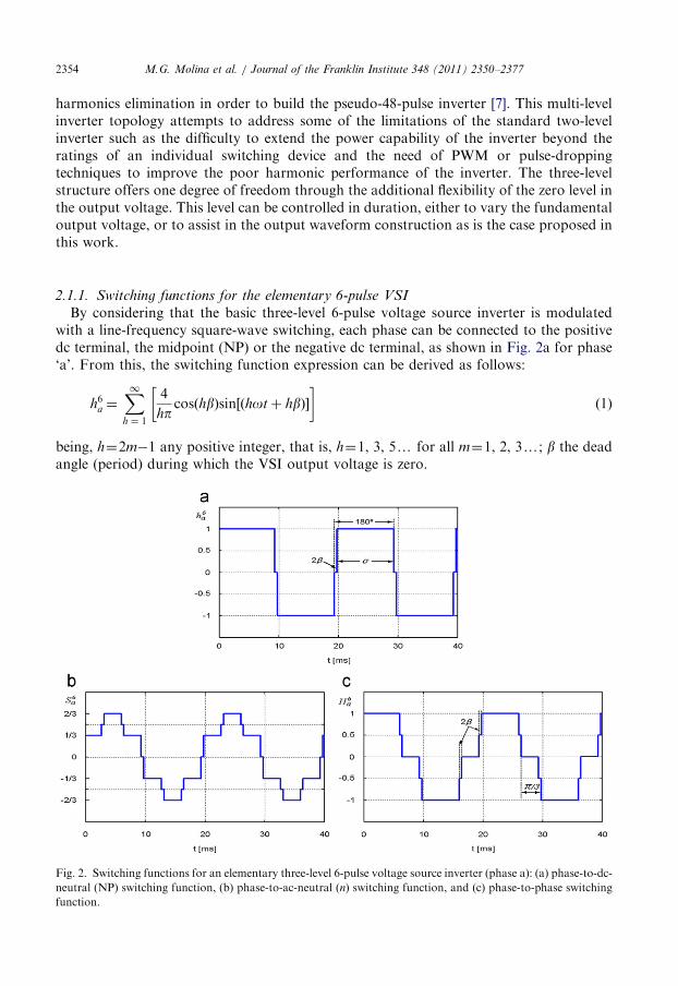
harmonics elimination in order to build the pseudo-48-pulse inverter [7]. This multi-levelinverter topology attempts to address some of the limitations of the standard two-levelinverter such as the difficulty to extend the power capability of the inverter beyond theratings of an individual switching device and the need of PWM or pulse-droppingtechniques to improve the poor harmonic performance of the inverter. The three-levelstructure offers one degree of freedom through the additional flexibility of the zero level inthe output voltage. This level can be controlled in duration, either to vary the fundamentaloutput voltage, or to assist in the output waveform construction as is the case proposed inthis work.
2.1.1. Switching functions for the elementary 6-pulse VSI
By considering that the basic three-level 6-pulse voltage source inverter is modulatedwith a line-frequency square-wave switching, each phase can be connected to the positivedc terminal, the midpoint (NP) or the negative dc terminal, as shown in Fig. 2a for phase‘a’. From this, the switching function expression can be derived as follows:
h6a ¼
X1h ¼ 1
4
hpcosðhbÞsin ðhotþ hbÞ½ �
� �ð1Þ
being, h¼2m�1 any positive integer, that is, h¼1, 3, 5y for all m¼1, 2, 3y; b the deadangle (period) during which the VSI output voltage is zero.
Fig. 2. Switching functions for an elementary three-level 6-pulse voltage source inverter (phase a): (a) phase-to-dc-
neutral (NP) switching function, (b) phase-to-ac-neutral (n) switching function, and (c) phase-to-phase switching
function.

M.G. Molina et al. / Journal of the Franklin Institute 348 (2011) 2350–2377 2355
The switching functions for phases ‘b’ and ‘c’ are similar but phase-shifted 1201 and2401, respectively. Assuming that the dc capacitors voltages are balanced and equal toVd/2, the VSI instantaneous terminal voltages with respect to the neutral point (NP) of thedc bus can be obtained as
vinv,a0
vinv,b0
vinv,c0
264
375¼
h6a
h6b
h6c
264
375Vd
2ð2Þ
In the same way, the instantaneous 6-pulse inverter output voltages with respect to theneutral (n) of the transformer ‘1Y’ can be expressed as
vinv,an
vinv,bn
vinv,cn
264
375¼
S6a
S6b
S6c
264
375Vd ð3Þ
where
S6a ¼
1
2h6
a�h6
a þ h6b þ h6
c
3
� �� �ð4Þ
Substitution of Eq. (1) into Eq. (4) yields the expression of the switching function forphase ‘a’ with respect to the neutral of the transformers (see Fig. 2b), as follows:
S6a ¼
X1h ¼ 1
2
hpcosðhbÞsinðhotþ hbÞ
� �ð5Þ
being, h¼6m71 any positive integer, that is, h¼1, 5, 7y for all m¼0, 1, 2yIn the same manner, the phase-to-phase instantaneous VSI output voltages can be
written as
vinv,ab
vinv,bc
vinv,ca
264
375¼
H6a
H6b
H6c
264
375Vd ð6Þ
where
H6a ¼
1
2ðh6
a�h6bÞ ð7Þ
Eq. (7) can be re-written using Eq. (1) as follows (see Fig. 2c):
H6a ¼
X1h ¼ 1
4
hpsin
hp3
� �cosðhbÞcos hotþ hb�
hp3
� �� �ð8Þ
being, h¼6m71 any positive integer, that is, h¼1, 5, 7y for all m¼0, 1, 2yIt is significant to observe the relationship between the fundamental and harmonic
components of the phase-to-phase and phase-to-neutral VSI output voltages, derived fromEqs. (5) and (8). The amplitude of the phase-to-phase voltages is
ffiffiffi3p
times the phase-to-neutral values, whereas the phase-shift is 301. Harmonic components different fromh¼6m71 are present although with phase opposition and therefore neutralized in theelementary three-level inverter.

M.G. Molina et al. / Journal of the Franklin Institute 348 (2011) 2350–23772356
2.1.2. Switching functions for the proposed equivalent 48-pulse VSI
By applying Fourier analysis to the inverter phase output voltages expressed by Eq. (3),as can be directly derived from Eq. (5), the peak value of the fundamental and harmonicscomponents can be found as follows:
v6inv ¼2
hpcosðhbÞVd ð9Þ
with h¼6m71 (h¼1, 5, 7, 11, 13y) and m¼0, 1, 2y .The harmonics content of the output voltage waveform, measured through the total
harmonic distortion (THD) of the basic 6-pulse VSI, is higher than 14%. In order to reducethe voltage THD and thus to fulfill with standards for power electronics equipments appliedto high voltage power systems (IEEE, CIGR �E, and UIE), an equivalent 48-pulse VSItopology is used as shown in Fig. 1. Thus, using zigzag phase-shifting transformers and theappropriate valves switching phase, the principle of harmonic neutralization can be applied.The combination of two three-level 6-pulse basic inverters (couples 1Y-1D and 2Y-2D)
through the appropriate magnetic coupling creates a three-level 12-pulse converter. The 301phase-shift between the primary and secondary of transformers 1 D and 2 D permits to cancelharmonics 5þ12r (i.e., h¼5, 17, 29, 41y) and 7þ12r (7, 19, 31, 43y), where r¼0,1,2,yIn the same way, by combining two three-level 12-pulse VSIs, phase-shifted 7.51 from eachother, a three-level 24-pulse inverter is build. This structure is able to behave like anequivalent standard two-level 48-pulse inverter for an optimum setting of b. The 151 phaseshift between the two groups of transformers (1Y-1D leading by 7.51 and 2Y-2D lagging by7.51) allows cancellation of harmonics 11þ24r (11, 35,y) and 13þ24r (13, 37,y). As all 3r
harmonics are not transmitted by the Y and D transformers’ secondaries, the first harmonicswhich are not cancelled by the transformers are 23rd, 25th, 47th, and 49th.A particular harmonic h reaches zero when Eq. (10) is satisfied:
2b¼1801
hð10Þ
Thus, by choosing an appropriate conduction angle s for the three-level inverters(s¼1801�2b), that is, soptimum¼172.51 (boptimum¼3.751), the 23rd and 25th harmonics canbe minimized, as can be observed from harmonic content shown in Fig. 3a. As a result, thefirst significant harmonics are the 47th and 49th, so that the inverter acts as a 48-pulseconventional VSI. This topology permits to generate an almost sinusoidal voltage waveformconsisting of 48-steps, as shown in Fig. 3b for a capacitive operation mode (generating
Fig. 3. Equivalent 48-pulse VSI-based STATCOM voltage THD and output waveforms for optimum conduction
angle operation: (a) voltage harmonic content and (b) voltage and current output waveforms.

M.G. Molina et al. / Journal of the Franklin Institute 348 (2011) 2350–2377 2357
reactive power). The low harmonic rate of the proposed 48-pulse VSI device is expressedthrough the reduced voltage THD, which is less than 3%. Consequently, this equipment canbe used in high power applications without ac filters. Even more, this controller supplies atthe point of common coupling (PCC) to the electric grid an almost sinusoidal current; thecurrent being smoothed by the leakage inductance of the step-up coupling transformers whichact as a natural first-order low-pass filter.
The switching function for the equivalent 48-pulse voltage source inverter can beestimated for phase ‘a’ by Eq. (11):
Se48a �
X1h ¼ 1
2
hpkT cosðhbÞsinðhotÞ
� �ð11Þ
with h¼48m71 (h¼1, 47, 49y) and m¼0, 1, 2y; kT¼4(n2/n1) the total voltage ratio ofthe zigzag phase-shifting transformers.
If the switching functions are averaged, approximating by their fundamentalcomponents (neglecting harmonics), the peak value of the phase-to-neutral output voltagefor the equivalent 48-pulse VSI can be expressed through Eq. (12):
Vinv ¼ Se48av Vd ð12Þ
being, Se48av ¼ ð2=pÞkT cosb is the average switching function for the equivalent
48-pulse VSI.The current exchange between the VSI and the ac system is straight determined by the
voltage across the tie reactance provided by the leakage inductance of the couplingtransformers. In this way, by varying the amplitude of the output voltages produced by theSTATCOM respect to the ac system voltage (PCC), the current flow can be controlled andthus the reactive power exchange. The magnitude of the STATCOM fundamental currentcomponent can be derived in the following fashion:
Im ¼1
oLVm�
2
pkT cosbVd
� �� �ð13Þ
where Vm is the maximum level of the ac system voltage at PCC and L the equivalentleakage inductance of the four coupling step-up transformers.
It is to be noted that if the amplitude of the inverter fundamental output voltage isincreased above that of the ac system (Vp), that is Vpo0.6663kT cos bVd, then the invertergenerates reactive (capacitive) power. In a similar way, if the amplitude of the inverterfundamental output voltage is decreased below that of the ac system, that is Vp40.6663kT cos bVd, then the VSI generates reactive (inductive) power. The active power generation(or absorption) in turns, is accomplished by phase-shifting (leading or lagging) the outputVSI voltage, vinv by an angle a in relation to the ac system voltage.
The total dc bus current expression can be derived from the contribution of each ac linecurrent through the switching functions. Thus, by considering a pure sinusoidal currentwaveform, as expressed by Eq. (14) for phase ‘a’:
ia ¼ Im sinðotþ jÞ ð14Þ
being ib and ic phase-shifted successively by 1201. j the phase-shift between the output linecurrent and the voltage generated by the STATCOM VSI.
The angle j is near equal to 7p/2 depending upon whether the STATCOM exchangescapacitive or inductive reactive power, respectively.

Fig. 4. Instantaneous dc bus current and voltage for the equivalent 48-pulse inverter in capacitive and inductive
mode: (a) dc bus current and (b) dc bus voltage.
M.G. Molina et al. / Journal of the Franklin Institute 348 (2011) 2350–23772358
The total dc bus current can be described by Eq. (15):
Idc ¼ Se48a Se48
b Se48c
h i ia
ib
ic
264
375 ð15Þ
This current waveform is shown in Fig. 4a for the inverter generating (capacitive mode)and absorbing (inductive mode) reactive power and neglecting losses. The switchingfunctions can be expressed in Fourier series form, so that Eq. (15) can be re-written as
Idc ¼ Id þX1h ¼ 1
3Im
48hsinð48hotÞ
� �ð16Þ
In case that active power is also exchanged, j will differ from 7p/2 in Eq. (14), beingreduced its absolute value. This feature also becomes evident in Eq. (16) by the appearanceof a constant dc current offset which produces a dc power. This dc current component Id,accounts for the total actual switching VSI losses and capacitors power losses, as well asthe current provided by the SMES coil linked to the dc bus. On the other hand, the infinitesummation of Eq. (16) describes the reactive power exchanged with the utility system.It can be noted the presence of harmonic components of order 48h on the capacitorscurrent, so that the first significant harmonic is the 48th. This feature meets the harmonicstransfer condition from ac-side to dc-side and vice versa. A harmonic on the dc-side istransferred to the ac-side as two side-bands of order (48h71) with positive and negativesequence components, respectively. In the same way, a given sequence harmonic on the ac-side transferred to the dc-side gives only one of the side-bands, being the lower order for apositive sequence and the higher order for a negative sequence.The previous study supposes a constant dc voltage provided by an infinite capacitor. If a
finite capacitor is considered, a dc ripple appears which depends on the capacitor value andthe current flow. Considering this case, as can be seen from Fig. 4b, the dc bus voltage canbe expressed in a similar way than for the dc bus current as follows:
Vdc ¼2
Cd
Z t
0
Idc dtþ Vd0 ð17Þ
being Vd0 an initial condition at t¼0.

M.G. Molina et al. / Journal of the Franklin Institute 348 (2011) 2350–2377 2359
Substituting Eq. (16) into Eq. (17) permits to obtain the dc bus voltage expression as
Vdc ¼Vd�X1h ¼ 1
6Im
48hZdðhÞcosð48hotÞ
� �ð18Þ
where Zd(h)¼ (1/48hoCd) is the dc side impedance at harmonic components 48h, neglectinglosses.
The dc voltage component, Vd involves initial voltage condition (according to capacitorsinitial state of charge) and active power exchanged with the utility system including theaction of the SMES coil. In contrast, the infinite summation describes the reactive powerexchanged with the ac system.
2.2. Two-quadrant three-level dc–dc converter
The inclusion of a SMES coil into the dc bus of the STATCOM demands the use of aninterface to adapt the wide range of variation in voltage and current levels between bothdevices. Controlling the SMES coil rate of charge/discharge requires varying as much thecoil voltage magnitude as the polarity according to the coil state-of-charge, while keepingessentially constant the STATCOM dc bus voltage. To this aim, a two-quadrant three-level dc–dc converter or chopper is proposed to be employed. This converter (top left-handside of Fig. 1) allows decreasing the ratings of the overall power devices by regulating thecurrent flowing from the SMES coil to the inverter of the STATCOM and vice versa.In addition, it allows varying the amplitude of the output voltage of the VSI, keepingconstant the conduction angle s of the inverter valves. Thus, the harmonic distortion of theSTATCOM output voltage can be maintained at the lowest level, independently of thevoltage required at the PCC (soptimum seen in Section 2.1.2).
Major advantages of three-level chopper topologies compared to traditional two-level onesinclude reduction of voltage stress of each thyristor by half, permitting to increase the chopperpower ratings maintaining high dynamic performance and decreasing the harmonics distortionproduced. Furthermore, the availability of redundant switching states, which allow generatingthe same output voltage vector through various states. This last feature is very significant inorder to reduce switching losses and dc current ripple, but mainly to maintain the charge balanceof the dc capacitors. This condition of NP voltage balancing is crucial for avoiding contributingadditional distortion to the three-level equivalent 48-pulse VSI output voltage.
Table 1
Three-level chopper output voltage vectors and their corresponding GTO switching states.
States G1 G2 G3 G4 Vab
1 1 1 1 1 þVd
2 0 0 0 0 �Vd
3 0 1 0 1 0
4 1 0 1 0 0
5 1 1 0 0 0
6 1 1 0 1 þVd/2
7 1 1 1 0 þVd/2
8 1 0 0 0 �Vd/2
9 0 1 0 0 �Vd/2

M.G. Molina et al. / Journal of the Franklin Institute 348 (2011) 2350–23772360
Table 1 shows all possible combinations of the chopper output voltage vectors, Vab
(defining the SMES side of the circuit as the output side) and their corresponding GTOswitching states. The addition of an extra level to the dc–dc chopper allows enlarging itsdegrees of freedom. As a result, the charge balance of the dc bus capacitors can be controlledusing the extra switching states, at the same time acting as a conventional dc–dc converter.The output voltage vectors can be selected based on the required SMES coil voltage and dcbus NP voltage. In this way, multiple subtopologies can be used in order to obtain outputvoltage vectors of magnitude 0 and Vd/2, in such a way that different vectors of magnitudeVd/2 produce opposite currents flowing from/to the neutral point. This condition causes afluctuation in the NP potential which permits to maintain the charge balance of the dc-linkcapacitors. By properly selecting the duration of the different output voltage vectors, anefficient dc–dc controller with NP voltage control capabilities is obtained.The dc–dc chopper has basically three modes of operation, namely the buck or charge
mode, the boost or discharge mode and the stand-by mode. These modes are obtained inthis work using a buck-boost topology control mode in opposition to a bang–bang controlmode [15] that is much simpler yet produces higher ac losses in the SMES coil.
2.2.1. Switching functions for the chopper operating in buck mode (charge)
In the charge mode, the chopper works as a step-down (buck) converter. This topologymakes use of switching states 1, 5, 6 and 7, in order to produce output voltage vectors þVd,0, and þVd/2 with separate contribution of charge at the NP from capacitors Cd1 and Cd2.In this mode, thyristors G1 and G2 are always kept on, while thyristors G3 and G4 aremodulated to obtain the appropriate output voltage, Vab, across the SMES coil. In thisway, only subtopologies closest to the state 1 are used. In consequence, only onesemiconductor device is switched per switching cycle Ts; this reducing the switching lossescompared to the standard two-level converter and thus also reducing the current ripple.Fig. 5a shows the switching function of the three-level chopper operating in buck mode.
This function, which is stated in Eq. (19), shows an attribute of immutability associated to theswitching states utilized for maintaining the charge balance of the dc capacitors (states 6 or 7):
Sch ¼D1 þD2 þX1h ¼ 1
2sinðhpD2Þ
hpcos hoðt�g2�2g1Þ� �� �
þX1h ¼ 1
sinð2hpD1Þ
hpcos hoðt�g1Þ� �� �
ð19Þ
Fig. 5. Chopper switching function and output current for buck mode (charge): (a) chopper switching function
and (b) SMES current.

M.G. Molina et al. / Journal of the Franklin Institute 348 (2011) 2350–2377 2361
where h¼1, 2, 3y; D1¼ (ton1/2Ts) the duty cycle for switching states 6 or 7; D2¼ (ton2/Ts) theduty cycle for switching state 1; g1¼ (D1/f) the harmonic phase angle due to D1; g2¼ (D2/2f)the harmonic phase angle due to D2.
It can be inferred from Eq. (19) the presence of voltage ripples generated by the three-level dc–dc chopper output. Even though this chopper has an improved harmonic qualityof the output voltage relative to the two-level converter, especially at low frequencies, it isnecessary to provide the SMES coil with a capacitive filter to prevent an excessive stress ofthe superconducting coil insulation caused by resonances at certain frequencies.
The relationship between the chopper output voltage Vab, and the VSI dc bus voltage Vd
can be derived from Eq. (19), as follows:
Vab ¼ SchVd ð20Þ
In the same fashion, the chopper output current Isc, i.e., the current flowing to the SMEScoil, can be estimated as described by Eq. (21):
Isc ¼1
L
Z t
0
Vab dt ð21Þ
Fig. 5b allows observing the existence of ripple also in the SMES coil current, althoughbeing lower than the case of the output voltage.
Once completed the charging of the SMES coil, the operating mode of the converter ischanged to the stand-by mode, for which only the state 5 is used. In this condition,thyristors G3 and G4 are switched off, while thyristors G1 and G2 are kept on all the time.During periods when the SMES coil is charged but it is expected not to use such storedenergy for a relatively long time, the coil should be shorted by a mechanical switch (Sw) inorder to avoid power dissipation on semiconductors.
2.2.2. Switching functions for the chopper operating in boost mode (discharge)
In the discharge mode, the chopper operates as a step-up (boost) converter in collaborationwith the dc bus capacitors. This topology employs switching states 2, 5, 8, and 9, in order toproduce at terminals ab, vectors �Vd, 0, and �Vd/2 with independent contribution of chargeat the NP from capacitors Cd1 and Cd2. In this mode, thyristors G3 and G4 are constantly keptoff while thyristors G1 and G2 are controlled to obtain the suitable voltage Vab, across theSMES coil. In this way, only subtopologies closest to state 2 are utilized.
Fig. 6a shows the switching function of the three-level chopper operating in discharge orboost mode. From this, the switching function expression can be derived as stated in Eq. (22).
Fig. 6. Chopper switching function and output current for boost mode (discharge): (a) chopper switching
function and (b) SMES current.

M.G. Molina et al. / Journal of the Franklin Institute 348 (2011) 2350–23772362
This function exhibits an analogous feature of immutability respect to the switching statesutilized for generating vectors �Vd/2 (states 8 or 9), as in the case of the buck mode:
Sdch ¼ 1�D1�D2 þX1h ¼ 1
2sinðhpð1�D2ÞÞ
hpcos hoðt�z2�2z1Þ½ �
� �þX1h ¼ 1
sinð2hpð1�D1ÞÞ
hpcos hoðt�z1Þ½ �
� �
ð22Þ
where h¼1, 2, 3y; z1¼ ((1�D1)/f) is the harmonic phase angle due to D1; z2¼ ((1�D2)/2f)the harmonic phase angle due to D2.As in the case of the chopper working in buck mode, the relationship between the chopper
voltage Vab, and the VSI dc bus voltage Vd can be derived from Eq. (22), as stated in Eq. (23):
Vab ¼ SdchVd ð23Þ
In the same manner, the SMES coil current Isc can be estimated as described by Eq. (21)for charge mode, but substituting Vab from Eq. (23) into Eq. (21).As can be inferred from previous equations, there exists also voltage and current ripples
generated by the three-level dc–dc chopper output in the boost mode. Fig. 6b shows theSMES coil current in the discharge or boost mode.By averaging the switching functions Sch and Sdch, which results analogous to neglecting
harmonics, a general expression relating the chopper average output voltage Vab, to theVSI average dc bus voltage Vd, can be derived through Eq. (24):
Vab ¼mVd ð24Þ
being m, the modulation index expressed as m¼ (D1þD2) the chopper buck mode (charge);m¼�(1�D1�D2) the chopper boost mode (discharge).
2.3. Multi-segment SMES coil
The equivalent circuit of the SMES coil depicted at the bottom left-hand side of Fig. 1makes use of a lumped parameters network represented by a six-segment modelcomprising self-inductances (Li), mutual couplings between segments (i and j, Mij), acloss resistances (Rsi), skin effect-related resistances (Rpi), turn-ground (shunt—CShi), andturn–turn capacitances (series—CSi). This model is based on the ones previously proposedin [16,17], and is reasonably accurate for electric systems transients studies, over afrequency range from dc to several thousand Hertz.
Fig. 7. SMES coil terminal impedance Zab versus frequency: (a) magnitude of SMES coil impedance and
(b) phase angle of SMES coil impedance.

M.G. Molina et al. / Journal of the Franklin Institute 348 (2011) 2350–2377 2363
Fig. 7 shows the frequency domain analysis of the six-segment SMES model (for the coildetailed in Appendix B), measuring the impedance of the superconducting coil across itsterminals (Zab). As can be seen from the magnitude of the terminal impedance, the coil hasparallel resonance frequencies at around 70, 120, and 200 Hz and series resonancefrequencies at about 110 and 190 Hz. As expressed in Section 2.2, the Fourier series of thechopper output voltage Vab, contains both even and odd harmonics of the switchingfrequency, which may excite coil resonances and cause significant voltage amplification oftransients with the consequent addition of insulation stress within the coil. Since the SMEScoil has a rather high inductance, these resonance frequencies become lower, turning thisphenomena an issue for selecting the chopper operating frequency. In addition, high powerdc–dc converters utilize low operating frequencies in order to minimize losses, beingsignificant in consequence to take into consideration the coil resonance phenomena forchoosing a safety frequency band of operation for the chopper.
Fortunately, the negative effects of the harmonic decrease faster than the inverse of theharmonic order due to the skin effect occurring in the superconductor. Furthermore,the inclusion of surge capacitors (Cs1 and Cs2) in parallel with grounding-balance resistors(Rg1 and Rg2) allows reducing the effect of resonances. However, in order to decreaseeven more this phenomenon, a filter capacitor CF is proposed to be connected at the SMEScoil terminals. Thus, a reduction of harmonics content of Vab is obtained, also stronglydecreasing the magnitude of the terminal SMES coil impedance at secondary series andparallel resonances, maintaining constant their frequencies and becoming lower thefrequency of the first parallel resonance, as shown in Fig. 8. In this way, for the casepresented here, the chopper operating frequency can be set as low as 500 Hz withoutproducing severe voltage amplification inside the SMES coil.
3. Multi-level control scheme of the STATCOM-SMES
The proposed three-level control scheme of the integrated STATCOM-SMES controlleris based on the steady-state average model of the device. This hierarchical control system,consisting of an external, middle and internal level, is based on concepts of instantaneouspower on the synchronous-rotating d–q reference frame [18], as shown in Fig. 9.
Fig. 8. SMES coil terminal impedance versus frequency with and without input filter.

Fig. 9. Proposed three-level control scheme of the STATCOM-SMES device.
M.G. Molina et al. / Journal of the Franklin Institute 348 (2011) 2350–23772364
3.1. External level control design
The external level control, which is outlined in Fig. 9 (left-hand side), is responsible fordetermining the active and reactive power exchange between the STATCOM-SMES deviceand the utility system in order to reduce the change of determined operating conditions ofthe power system in case of large disturbances. This control strategy is designed forperforming two major objectives (control modes) with dissimilar priorities:
�
Frequency control mode (FCM). Case of a STATCOM-SMES controller with activeand reactive power exchange capabilities. � Voltage control mode (VCM). Case of a traditional STATCOM with only reactivepower compensation capabilities.
3.1.1. Frequency control mode
This highest-priority control mode accomplished by the middle blocks of the external levelaims at controlling the PS frequency through the modulation of both, the reactive component ofthe output current iq (case of a conventional STATCOM) and the active component id (case of aSTATCOM-SMES). In the case of controlling iq, the set-point of the VCM, i.e., the voltagereference signal Vr, is varied with a stabilizing voltage signal proportional to the PS frequencydeviation Df (defined as the difference between the set reference frequency fr and the actualfrequency f) which directly represents the power oscillation of the PS. This added signal causesthe output quadrature current of the STATCOM, iq to vary around the operating point definedby Vr, the purpose of this variation being to improve the damping of the power oscillations. Inthis way, the voltage at the PCC is forced to decrease when the frequency deviation Df is positiveaiming at reducing the transmitted power through the transmission system and thus providingan effective fast-acting voltage reduction reserve which opposes the deceleration of generators inthe PS. This action is performed in the opposite way when the frequency deviation Df isnegative, and then generators accelerate. Two transfer functions, including a lag-compensator(LC2), are used to assist in shaping the gain and phase characteristics of the frequency stabilizerfor the case of modulating the output quadrature current of the STATCOM.

M.G. Molina et al. / Journal of the Franklin Institute 348 (2011) 2350–2377 2365
Although the power oscillation damping technique of the standard STATCOM is rathereffective, the most effective compensation action for power oscillations (or swings) dampingand thus for primary frequency control (PFC) is carried out by rapidly exchanging active powerwith the utility system, that is to say by controlling the output direct current of the STATCOM-SMES, id. Considering this case, as in the previous case, the reference of the STATCOM-SMESoutput direct current is directly derived from Df, representing the power oscillation of thesystem. The frequency transducer transfer function is designed to eliminate any dc componentthat may be present on the signal Df, by proper setting of the constant Ttrf of the low-pass filter.Since a robust and efficient frequency control scheme requires the effective damping of a widerange of generators power oscillations, ranging from less than 0.2 Hz for global oscillations to4 Hz for local oscillations of units, a decoupled two-loop control approach with differentialbands of damping is proposed in this work. Thus, a loop is dedicated to low and intermediatefrequency modes of oscillations while the other one covers the high frequency mode.
The first loop is composed of a proportional-integral (PI) controller (PI4) with outputrestriction including an anti-windup system to enhance the dynamic performance of the PFCsystem. A speed-droop Rf (typically 3%) is also included in order to obtain a stable loaddivision among several fast-response devices operating in parallel. This characteristic isanalogous to the one included in generators speed governors. Thus, the rapid active powerexchange between the STATCOM-SMES and the PS is controlled, forcing the SMES coil toabsorb active power when generators accelerate (charge mode), or to inject active power whenthey decelerate (discharge mode). The PI controller including a droop feedback acts as anoverall first-order lag-compensator. This first loop ensures an excellent performance in dampingpower oscillations at low and intermediate frequency modes and then for large-signal stability,but its response is very poor for the high frequency mode. To this end, a supplementary signalproportional to the rate of change of the system frequency has been included via the secondloop in order to speed-up the transient response of the controller for managing high frequencymodes of oscillations. A differential signal of the frequency error with restricted high frequencygain is obtained using a first-order washout filter. A lag-compensator (LC1) is also included intothe loop in order to improve the dynamic response of the controller and to ensure the robustglobal damping provided by the proposed PFC mode. This second loop provides an excellentperformance in damping power oscillations at high frequency modes and then for small-signalstability. Therefore, both loops act independently, so that their effects add up to provideeffective damping of all modes of interest. In this way steady state and transient objectives arefulfilled by this control strategy almost uniformly. The stabilizer signal composed from bothloops is passed through a final limiter for setting the reference idr.
In all cases, the frequency signal is derived from the positive sequence components of theac voltage vector measured at the PCC of the STATCOM-SMES, through a phase lockedloop (PLL). The design of the PLL is developed in the dq reference frame and incorporatesan adaptive control using a neural network for increasing its capture range [19]. Thisdevice also synchronizes, by providing the phase y, the coordinate transformations fromabc to dq components in the voltage and current measurement system. These signals arethen filtered using second-order low-pass filters in order to obtain the fundamentalcomponents employed in the control system.
3.1.2. Voltage control mode
This subordinate control mode has the goal of controlling (supporting and regulating)the voltage at the PCC to the electric grid. It has proved very good performance in

M.G. Molina et al. / Journal of the Franklin Institute 348 (2011) 2350–23772366
conventional STATCOM controllers through the modulation of the reactive componentof the output current iqr. To this end, in this work the instantaneous voltage at the PCCis computed using a synchronous-rotating reference frame. In consequence, by applyingPark’s transformation, the instantaneous values of the three-phase ac bus voltages aretransformed into d–q components, vd and vq, respectively. By defining the d-axis alwayscoincident with the instantaneous voltage vector v, then vd results equal to 9v9 while vq is setat zero. Consequently, only vd is used for computing the voltage error vector which isintroduced to a proportional-integral (PI) controller with output restriction including ananti-windup system to enhance the dynamic performance of the VCM system. A voltageregulation droop Rd (typically 5%) is included in order to allow a higher operation stabilityof the STATCOM-SMES device in cases that more high-speed voltage compensators areoperating in the area. This characteristic is comparable to the one included in generatorsvoltage regulators [20]. As a result, the PI controller including a droop feedback acts as anoverall first-order lag-compensator.
3.2. Middle level control design
The middle level control makes the expected output, particularly the actual active andreactive power exchange between the STATCOM-SMES and the ac system, todynamically track the reference values set by the external level. The middle level controldesign, which is depicted in Fig. 9 (middle side), is based on a linearization of the state-space averaged mathematical model of the STATCOM VSC in the d–q reference framedescribed in depth in [7], as follows:
s
d
q
d
dp
e
d
e
d
s
e
s
s
s
e
s
s
d
q
dLv
Vii
CRS
CS
C
L
S
LR
LS
LR
Vii
s
qd
q
d
ð25Þ
where Rs is the equivalent resistance accounting for transformers winding resistance andVSI semiconductors conduction losses, Ls
0 the equivalent leakage inductance in the d–q
reference frame for the four VSI step-up transformers, Cd the equivalent capacitance of thedc bus capacitors, and o the synchronous angular speed of the network voltage at thefundamental system frequency f.As reported by Acha et al. [21], modeling of static inverters using a synchronous-
rotating orthogonal d–q reference frame offers higher accuracy than employing stationarycoordinates. Moreover, this operation allows designing a simpler control system than usinga–c or a–b stationary components.The average switching functions for the equivalent 48-pulse voltage source inverter,
transformed into the d–q reference frame, can be defined as
Se48d ¼ Se48
av cosa ð26Þ
Se48q ¼ Se48
av sina ð27Þ

M.G. Molina et al. / Journal of the Franklin Institute 348 (2011) 2350–2377 2367
with a is the phase-shift of the VSI output voltage from the reference position, set by theinstantaneous voltage vector measured at the PCC.
The new coordinate system is defined where the d-axis is always coincident with theinstantaneous voltage vector at the PCC (vd¼9v9, vq¼0). Consequently, the d-axis currentcomponent contributes to the instantaneous active power p- and the q-axis currentcomponent represents the instantaneous reactive power q, as stated in Eqs. (28) and (29).In this way, in order to achieve a decoupled active and reactive power control, it is requiredto provide a full decoupled control strategy for id and iq:
p¼ 32ðvd id þ vqiqÞ ¼
329v9id ð28Þ
q¼ 32ðvd iq�vqidÞ ¼
329v9iq ð29Þ
Inspection of Eq. (25) shows a cross-coupling of both components of the STATCOM-SMES controller output current through o. Therefore, in order to decouple the control ofid and iq, appropriate control signals have to be generated. To this aim, it is proposed theuse of two control signals x1 and x2, which are derived from assumption of zero deriva-tives of currents (sid and siq) in the upper part (ac side) of Eq. (25). In this way, the cross-coupling effect in steady state can be eliminated. This upper part of Eq. (25) can bere-written using the relation stated in Eq. (12), transformed into the synchronous rotatingd–q reference frame through Eqs. (26) and (27), as follows:
sid
iq
" #¼
0
0
� �¼
�Rs
L0so
�o�Rs
L0s
26664
37775
id
iq
" #þ
1
L0s
vinvd�9v9
vinvq
" #ð30Þ
From Eq. (30), the peak value of the phase-to-neutral output voltage of the pseudo-48-pulse VSI, transformed into the d-q reference frame, can be directly derived as stated inEqs. (31) and (32):
vinvd¼L0s
Rs
L0sid�oiq
� �þ 9v9 ð31Þ
vinvq¼ L0s
Rs
L0siq þ oid
� �ð32Þ
Assigning the proposed control signals x1 and x2 in order to replace the output currentcomponents iq and id, respectively, in such a way that only the cross-coupling of bothcomponents are left in Eqs. (31) and (32), it is obtained:
vinvd¼L0sðx2�oiqÞ þ 9v9 ð33Þ
vinvq¼ L0sðx1 þ oidÞ ð34Þ
Eventually, substituting Eqs. (33) and (34) into the upper part (ac side) of Eq. (25), yieldsthe expression of Eq. (35) as follows:
sid
iq
" #¼
�Rs
L0s0
0�Rs
L0s
26664
37775
id
iq
" #�
x1
x2
" #ð35Þ

M.G. Molina et al. / Journal of the Franklin Institute 348 (2011) 2350–23772368
As can be noticed, id and iq respond to x1 and x2, respectively, with no crosscoupling.Thus, with the introduction of these new variables this control approach allows to obtain aquite effective decoupled control with the model (ac side) reduced to first-order functions.In order to guarantee the decoupled control condition of id and iq in steady state, twoconventional PI controllers with proper feedback of the STATCOM-SMES output currentcomponents are introduced in order to generate the proposed control signals x1 and x2, asshown in Fig. 9 (middle side).Even though the STATCOM-SMES and the power system are inherently nonlinear,
practical phase-shift ratings a of the VSI output voltage from the reference position aresmall enough (typically within 731) to consider the linearization of average switchingfunctions as valid. Consequently, linear methods of control yield satisfactory results for awide range of disturbances in the PS.Fig. 9 (middle side) shows the full implementation of the middle level control. The
coordinate transformation from Cartesian to Polar yields the required magnitude of theoutput voltage vector produced by the VSI (Vinv) and the phase-shift rating a of this vectorfrom the reference position, represented by the voltage vector measured at the PCC of theSTATCOM-SMES. From Vinv, the required voltage at the dc bus (Vdr) is derived andthe duty cycle of the chopper thyristors (D*) is estimated through a balance of dc power inthe chopper, taking into consideration the active power injection/absorption ratingsrequired from the STATCOM-SMES and the actual current of the SMES coil iL. The dutycycle of the chopper GTO thyristors is then derived by relying on the mode of operation ofthe dc/dc chopper (charge/discharge), so that an initial value Dini is determined for thethyristors duty cycle. This mode of operation is determined assessing the sign of therequired positive sequence component of id (idr1) via a charge/discharge selection block andproducing a signal of mode Sc/d that is also required by the internal level control.A corrective action of integral-type (PI controller) is needed for an accurate tracking of theactual duty cycle D*, being D* the total duty ratio of the three-level chopper. Therefore, dcbus voltage deviations DVd caused by actual VSC switching losses and capacitors powerlosses can be quickly counteracted. Finally, duty cycles D1 and D2 are computed from D*through a novel controller for balancing the dc link capacitors. This novel extra dc voltagecontrol block provides the availability of managing the redundant switching states of thechopper according to the capacitors charge unbalance measured through the neutral pointvoltage, VPN ¼V c1�Vc2. This specific loop modifying the modulating waveforms of theinternal level control is also proposed for reducing instability problems caused byharmonics as much in the STATCOM-SMES device as in the electric system [22].
3.3. Internal level control design
The internal level provides dynamic control of input signals for the dc–dc and ac–dcconverters. This level is responsible for generating the triggering and blocking controlsignals for the different valves of the pseudo-48-pulse three-level VSI and the three-leveldc–dc chopper, according to the control mode and types of valves used. Fig. 9 (right-handside) shows a basic scheme of the internal level control of the STATCOM-SMEScompensator. This level is mainly composed of a line synchronization module and a firingpulses generator for both the STATCOM VSI and the dc–dc chopper. The line synchroni-zation module simply synchronizes the STATCOM-SMES device switching pulses with the

M.G. Molina et al. / Journal of the Franklin Institute 348 (2011) 2350–2377 2369
positive sequence components of the ac voltage vector at the PCC through the PLL phasesignal, ys.
4. Computational implementation of the STATCOM-SMES model in MATLAB/Simulink
The full detailed model of the proposed STATCOM-SMES device is implemented in theMATLAB/Simulink software package [23] and uses the SimPowerSystems (SPS) as shown inFig. 10. Since this detailed model contains many states and non-linear blocks such as powerelectronics switches, the discretization of the electrical system with fixed-step is required soas to allow much faster simulation than using continuous variable time-step methods.Two sample times are employed in order to enhance the simulation, Ts_Power¼5 ms for thesimulation of the power system, the multi-pulse VSI and the dc–dc converter, andTs_Control¼100 ms for the simulation of the multi-level control blocks.
The Simulink/SPS libraries offer a variety of models, such as machines, power electronicdevices and control blocks, which make it feasible to straightforwardly develop the proposedtechnical models. Thus, the equivalent 48-pulse GTOs voltage source inverter is basically madeout of three-level bridge blocks linked through zigzag phase-shifting transformer blocksand series branches of RC linear elements, all being ready-built blocks and elements of SPS.The three-level GTOs dc–dc converter is wisely developed using an original proposal. Theconventional three-level bridge block with just one branch activated is employed in such a waythat simply the required semiconductors are switched while the others are kept off at all times.In this way, the dc–dc converter implementation is optimizely achieved for discrete simulations,since the turn-on and turn-off times (fall time and tail time) of the power switching device arenot modelled. This results in a faster simulation when compared to a single GTO mask because
Fig. 10. MATLAB/Simulink implementation of the proposed STATCOM-SMES detailed model.

M.G. Molina et al. / Journal of the Franklin Institute 348 (2011) 2350–23772370
of the later increased state-space model. Thus, the conventional solution with individualsemiconductors would not be feasible when the power system is also included into thesimulation. The six-segment SMES coil is developed using series branches of RC linearelements and the generalized model of mutual inductances block existing is SPS, specifying theinductance matrices that define the mutual coupling relationship between the six windings(balanced for this application). Protection elements, such as the metal-oxide varistors (MOVs)are developed via the metal-oxide surge arrester modelled through a highly nonlinear V–I
characteristic. In the same way, the bypass switch is made out of a circuit breaker controlledfrom an external Simulink signal.
5. Digital simulation results
5.1. Test system
The test power system used to study the dynamic performance of the STATCOM-SMESis shown in Fig. 11 as a single-line diagram. This 7-bus transmission system operates at230 kV/50 Hz, and implements a dynamically-modelled single generator-type small utilitylinked to a bulk power system represented by a machine-infinite bus-type used for studiesof FACTS devices. The generator is powered by a steam turbine represented through non-linear models and the controls of the unit include a dc type-1a standard IEEE voltageregulator and a speed governor. All loads are modelled by constant impedances and aregrouped at buses 6, 4, and 7. The major test system data are summarized in Appendix A.The performance of the proposed STATCOM-SMES controller is analyzed through
digital simulation carried out using SPS of MATLAB/Simulink during 40 s. To this aim, athree-phase-to-ground fault is applied at bus 2 in the bulk power system at t¼0.1 s, andcleared 5 cycles later (100 ms) by tripping the tie line with the opening of the circuit breakerplaced between buses 3 and 4. A load shedding scheme (LS) is included in order to preventthe system frequency collapse during the disturbance, but also to make use of the activatedload shedding steps as a performance comparison index for various scenarios including theSTATCOM-SMES. This integrated controller is placed at bus 4 aiming at enhancing thedynamic security, in cases that severe disturbances occur.
Fig. 11. Test system.

M.G. Molina et al. / Journal of the Franklin Institute 348 (2011) 2350–2377 2371
5.2. Base case study
For the topology presented in the test case without the inclusion of the STATCOM-SMES, also called as base case, in the steady state previous to the fault the utility systemmust import about 20 MW from the bulk power system. In this interconnected operationthe system frequency is at its rated value of 1 p.u. After the fault, the tie line is tripped andthe generator operates in island conditions. Under these conditions, only the generator isable to provide all the power demanded by loads. As can be seen from the simulationresults of Fig. 12, presented the base case using dash-dotted lines, the spinning reserve ofthe unit is neither sufficiently large nor fast enough for supporting the system frequencythrough the primary frequency control (PFC) and thus avoiding the frequency drop whichcauses the system collapse. In this case, the implementation of the automatic LS schemewith the activation of four (of ten) frequency steps is required in order to recover thesystem frequency to its scheduled value. Despite this fact, the generating unit have to rampup quickly to decrease the amount of load rejected. Load rejection also permits to improvethe voltage profile at bus 4 in each LS activation step. A transient overvoltage occurs untilunit’s voltage regulators stabilize the bus voltage.
Consider the inclusion at bus 4 of a 100 Mvar STATCOM controller combined with a30MW/400MJ SMES coil. In this condition, two external control modes are studied, namelythe voltage control mode, or VCM (case of a traditional STATCOM without energy storage)and the frequency control mode, or FCM (case of an integrated STATCOM-SMES controller).
5.3. STATCOM in voltage control mode
The impact of the inclusion of a traditional STATCOM controller at bus 4 operating in VCMcan be analyzed by simulation results of Fig. 12, portrayed this case through dashed lines. Thegood performance of the voltage regulator of the STATCOM device is evidently depicted by thecompensation of reactive power, which is shown in Fig. 13 in dash-dotted line. PI controllergains of the external level control scheme in VCMwere determined to give the power system thefastest possible Bus 4 voltage regulation (the shortest settling time, and therefore rise time) whilekeeping the maximum overshoot less than 15%. However, this control objective (VCM) of thestandard STATCOM device comes into conflict with the primary frequency control of the PS.Thus, by controlling the voltage at bus 4, an augment of the active power demanded of thegenerator is obtained which causes an increase of the system frequency drop and its rate ofchange. In this way, an extra LS frequency step needs to be activated respect to the base case
Fig. 12. Fault results for the proposed case studies: (a) power system frequency and (b) bus 4 voltage.

Fig. 13. STATCOM-SMES active and reactive power for VCM and FCM.
Fig. 14. Generator active power for the base case and STATCOM-SMES in FCM.
M.G. Molina et al. / Journal of the Franklin Institute 348 (2011) 2350–23772372
(five of ten steps) by the PFC in order to recover the system frequency during the disturbanceeffect. In the post-fault steady-state, the voltage level at bus 4 is enhanced by the STATCOMproviding a compensation of 47.5 Mvar (Fig. 13).
5.4. STATCOM-SMES in frequency control mode
The effect of incorporating a 30MW/400MJ SMES coil into the dc bus of the conventional100 Mvar STATCOM device, yielding an enhanced integrated STATCOM-SMES controller,can be studied through the simulation results of Fig. 12, depicted this case through solid lines.These results clearly show the outstanding dynamic performance of the frequency control modeof the STATCOM-SMES system. After the fault, when the frequency deviation exceeds thecontroller dead-band limits, the SMES device is activated. The rapid active power supply addedto the conventional reactive power compensation, which are shown in Fig. 13 in solid anddashed lines, respectively, absorbs the sudden power lost occurred after the tie-line tripping.Thus, the generator is able to find the balance with the load at a lower speed than in the previoustest cases without producing a significant frequency deviation, as can be derived from thegenerator active power flow of Fig. 14, for the base case (dashed lines) compared to the case withthe STATCOM-SMES in FCM (solid lines). This condition permits to greatly decrease thepower strain of the generating unit and also the spinning reserve required from this machine.

M.G. Molina et al. / Journal of the Franklin Institute 348 (2011) 2350–2377 2373
In this case, the effects of the disturbance are totally mitigated in a shorter time than in the basecase without being necessary to activate the load shedding scheme. In fact, the frequency dropis drastically reduced and maintained far away from the load shedding limit. Furthermore,the maximum reactive power required from the STATCOM-SMES is reduced respect to theconventional STATCOM device and the voltage profile at bus 4 is preserved without rejectingload. The improvement of the PFC is obtained by the action of the SMES coil, which providesactive power for about 20 s (approximately 315 MJ of energy). Automatic generation control(AGC) action has not been shown in order to focusing the study on the primary frequencycontrol performance.
6. Conclusions
In this paper, the operating characteristics of a static synchronous compensator(STATCOM) integrated with superconducting magnetic energy storage (SMES) for highpower applications in the transmission network level have been investigated. A detailedfull dynamic model of the integrated STATCOM-SMES device has been proposed,including a three-level pseudo-48-pulse voltage source inverter and a two-quadrant three-level dc–dc converter as interface between both devices. Based on the state-space averagingmethod a three-level control scheme has been designed, comprising an enhanced frequencycontrol scheme, a full decoupled current control strategy in the synchronous-rotating d-qreference frame with an effective control approach to balancing the STATCOM dc buscapacitors voltage. The proposed STATCOM-SMES controller has been implemented andfully validated by digital simulation carried out using SimPowerSystems of MATLAB/Simulink. The descriptive digital models proposed have been deeply examined, includinganalytical results and digital simulations of main ac and dc system variables.
Acknowledgments
The authors would like to thank Dr. Luis S. Zurlo (Ph.D. in Mathematics, formerlyUniversity of Iowa, USA, and nowadays Universidad Nacional de San Juan, Argentina)for his significant contribution to the mathematical development of this paper.
Appendix A
A.1. Test system data
Transmission lines are modelled as distributed parameters with lumped losses.Major lines data are given in Table A1, using p.u. quantities on 220 kV and 100 MVAbase. Table A2 shows the most important transformer data. In this case, all p.u. quantitiesare on 220 kV and the generating unit nominal MVA base. Major generating unit dataand the active and reactive power quantities used in the base-case load flow are shown inTable A3. In addition, main parameters related to synchronous machines, voltage regu-lator and prime mover systems are shown in Tables A4 and A5. Finally, in Table A6 themost important load data are shown.
An underfrequency load shedding scheme is utilized. The scheme is composed of tenfrequency steps, each one rejecting 5 MW and 2 Mvar. Consequently up to 50 MW of

Table A2
Transformer data.
ID# From Bus To bus R (pu) X (pu) G (pu� 10�3) B (pu� 10�3) SN (MVA) Np/Ns (kV/kV)
T1 6 5 0.00413 0.1653 0.653 3.0976 250 230/18
R and X¼winding resistance and reactance.
G and B¼magnetizing conductance and susceptance.
Np/Ns¼voltage transformation ratio.
Table A1
Line data.
ID# From Bus To Bus L (km) R (pu) X (pu) B (pu)
L1 2 3 170 0.0223 0.1227 0.2948
L2 5 4 45 0.0149 0.0818 0.1966
L3 4 7 35 0.0062 0.0341 0.0819
ID#¼component identifier; R, X, and B¼total positive sequence resistance, reactance and susceptance of
transmission lines.
Table A3
Generating unit data.
ID# Bus Unit Type Unit Size (MW) PG (MW) QG (Mvar) SN (MVA) VN (kV) VS (pu)
G1 6 ST 170 100 15 250 18 1.03
Unit type¼ST—fossil-fuelled steam turbine with tandem compound single mass generator.
PG and QG¼generating unit active and reactive power output.
VS¼generating unit voltage output.
Table A4
Generating unit data (cont.).
ID# H (MW/MJ) RS (pu) Xl (pu) Xd (pu) Xq (pu) Xd0 (pu) Xq
0 (pu) Td00 (s) Tq0
0 (s)
G1 5.5 0.001 0.14 1.569 1.548 0.324 0.918 5.140 1.5
H¼ inertia constant.
Rs and Xl¼stator resistance and leakage inductance Xd, Xd0, Xq, and Xq
0 ¼direct and quadrature axis synchronous
and transient reactances Td00 and Tq0
0 ¼direct and quadrature axis open-circuit transient and subtransient time
constants.
Table A5
Generating unit data (cont. 1).
ID# R (%) DB (mHz) TSR (ms) TSM (ms) KA TA (ms) KF TF (ms) TR (ms)
G1 5 180 1 150 300 1 0.001 100 20
R¼speed regulation or governor droop.
DB¼dead band of speed regulator.
TSR¼speed-relay time constant.
TSM¼servo-motor time constant.
M.G. Molina et al. / Journal of the Franklin Institute 348 (2011) 2350–23772374

Table A6
Load data.
ID# Bus PL MW QL Mvar LS
Ld7 7 120 32 Y
Ld4 4 3 0.95 N
Ld6 6 5 1.1 N
PL and QL¼ load active and reactive power.
LS¼ load shedding scheme (Y¼ included, N¼not included).
Table A7
Load-shedding scheme.
Frequency step f (Hz) f (p.u.)
1 48.539 0.97078
2 48.512 0.97024
3 48.475 0.9695
4 48.422 0.96844
5 48.369 0.96738
6 48.312 0.96624
7 48.25 0.965
8 48.185 0.9637
9 48.115 0.9623
10 48.042 0.96084
fmin, Admissible¼47.5 Hz¼0.95 p.u.
Table B1
STATCOM-SMES data.
Qmax (Mvar) Pmax (MW) ESC max (MJ) ISC max (kA) Vd (kV) Cd1,Cd2 (mF) LT (H)
100 96 400 4 24 10 50
Qmax¼maximum rated reactive power.
Pmax¼maximum rated active power.
ESC max¼maximum rated storage capacity of the SMES system.
ISC max¼maximum rated current of the superconducting coil.
Vd¼rated voltage of the dc bus.
Cd1, Cd2¼capacitances of the dc bus capacitors.
LT¼total inductance of the SMES device.
M.G. Molina et al. / Journal of the Franklin Institute 348 (2011) 2350–2377 2375
active power can be rejected, representing 41.66% of the active power load. The operatingtime delay of each load-shedding step, which utilizes solid-state relays, is 0.2 s (Table A7).
Appendix B
B.1. STATCOM-SMES controller data
Tables B1–B3 summarize the most important data corresponding to the STATCOM,chopper and SMES sub-systems.

Table B3
Chopper and SMES filter data.
TF (ms) TT (ms) VFG/VFD (V) RON (mO) CS1,CS2 (mF) Rg1,Rg2 (kO) CF (mF)
5 10 1/0.6 1 1.1 27.5 6
TF¼fall time of the GTO of the chopper (similar for the inverter).
TT¼ tail time of the GTO of the chopper.
VFG, VFD¼ forward voltages for GTOs and diodes, respectively.
RON¼ internal resistance of the GTO device.
CS1, CS2, CF¼capacitances of SMES filter.
Rg1, Rg2¼ground resistances.
Table B2
SMES model data.
#Seg. Li (H) Mij (H) CSi (mF) CShi (mF) Rpi (O) Rp (O)
6 8.334 3.12 0.01 0.488 0.05 5
#Seg.¼number of segments of the coil model.
Li¼self-inductance per segment.
Mij¼mutual coupling inductance between segments.
CSj¼series stray capacitance between turns of the coil.
CShj¼shunt stray capacitance between turn and ground.
Rpi¼ac loss resistance per segment.
Rp¼stray resistance between segments due to skin effect.
M.G. Molina et al. / Journal of the Franklin Institute 348 (2011) 2350–23772376
References
[1] M.H. Ali, B. Wu, R.A. Dougal, An overview of SMES applications in power and energy systems, IEEE
Transactions on Sustainable Energy 1 (1) (2010) 38–47.
[2] X.P. Zhang, C. Rehtanz, B. Pal, Flexible AC Transmission Systems: Modelling and Control (Power
Systems), 2nd Ed., Springer-Verlag, New York, 2009.
[3] S. Panda, Differential evolution algorithm for SSSC-based damping controller design considering time delay,
Journal of the Franklin Institute (2011). doi:10.1016/j.jfranklin.2011.05.011.
[4] S. Panda, N.P. Padhy, Optimal location and controller design of STATCOM for power system stability
improvement using PSO, Journal of the Franklin Institute 345 (2) (2008) 166–181.
[5] H.M. Solimana, A. Dabroumb, M.S. Mahmoudc, M. Soliman, Guaranteed-cost reliable control with
regional pole placement of a power system, Journal of the Franklin Institute 348 (5) (2011) 884–898.
[6] M.G. Molina, P.E. Mercado, E.H. Watanabe, Static synchronous compensator with superconducting magnetic
energy storage for high power utility applications, Energy Conversion and Management 48 (8) (2007) 2316–2331.
[7] M.G. Molina, P.E. Mercado, E.H. Watanabe, Improved superconducting magnetic energy storage (SMES)
controller for high power utility applications, IEEE Transactions on Energy Conversion 26 (2) (2011) 444–456.
[8] J. Holtz, Pulsewidth modulation—a survey, IEEE Transactions on Industrial Electronics 39 (5) (1992) 410–420.
[9] J. Rodriguez, J.S. Lai, F.Z. Peng, Multilevel inverters: a survey of topologies, controls, and applications,
IEEE Transactions on Industrial Electronics 49 (4) (2002) 724–738.
[10] F.Z. Peng, J.S. Lai, J.W. McKeever, J. Van Coevering., A multilevel voltage-source inverter with separate
DC sources for static VAr generation, IEEE Transactions on Industry Applications 32 (5) (1996) 1130–1138.
[11] J.S. Lai, F.Z. Peng, Multilevel converters—a new breed of power converters, IEEE Transactions on Industry
Applications 32 (3) (1996) 509–517.
[12] M.G. Molina, P.E. Mercado, Controlling a static synchronous compensator with superconducting magnetic
energy storage for applications on primary frequency control, Latin American Applied Research Journal
34 (2) (2004) 119–126.

M.G. Molina et al. / Journal of the Franklin Institute 348 (2011) 2350–2377 2377
[13] M.S. El-Moursi, A.M. Sharaf, Novel controllers for the 48-pulse VSC STATCOM and SSSC for voltage
regulation and reactive power compensation, IEEE Transactions on Power Systems 20 (4) (2005) 1985–1997.
[14] D. Soto, T.C. Green, A comparison of high-power converter topologies for the implementation of FACTS
controllers, IEEE Transactions on Industrial Electronics 49 (5) (2002) 1072–1080.
[15] M.V. Aware, D. Sutanto, SMES for protection of distributed critical loads, IEEE Transactions on Power
Delivery 19 (3) (2004) 1267–1275.
[16] L. Chen, Y. Liu, A.B. Arsoy, P.F. Ribeiro, M. Steurer, M.R. Iravani, Detailed modeling of superconducting
magnetic energy storage (SMES) system, IEEE Transactions on Power Delivery 21 (2) (2006) 699–710.
[17] M. Steurer, W. Hribernik, Frequency response characteristics of a 100 MJ SMES coil—measurements and
model refinement, IEEE Transactions on Applied Superconductivity 15 (2005) 1887–1890.
[18] P.C. Krause, Analysis of Electric Machinery, Mc Graw-Hill, New York, 1992.
[19] M. Raoof, A.A. Suratgar, Adaptive control of PLL using neural network, Journal of the Franklin Institute
346 (1) (2009) 81–93.
[20] H. Gozde, M. Cengiz Taplamacioglu, Comparative performance analysis of artificial bee colony algorithm
for automatic voltage regulator (AVR) system, Journal of the Franklin Institute (2011). doi:10.1016/
j.jfranklin.2011.05.012.
[21] E. Acha, V. Agelidis, O. Anaya-Lara, T. Miller, Power Electronic Control in Electrical System, 1st ed.,
Newness, United Kingdom, 2002.
[22] M.G. Molina, P.E. Mercado, Power flow stabilization and control of microgrid with wind generation by
superconducting magnetic energy storage, IEEE Transactions on Power Electronics 26 (3) (2011) 910–922.
[23] The MathWorks Inc. SimPowerSystems for use with Simulink 7.6: User’s Guide, 2010.

本文献由“学霸图书馆-文献云下载”收集自网络,仅供学习交流使用。
学霸图书馆(www.xuebalib.com)是一个“整合众多图书馆数据库资源,
提供一站式文献检索和下载服务”的24 小时在线不限IP
图书馆。
图书馆致力于便利、促进学习与科研,提供最强文献下载服务。
图书馆导航:
图书馆首页 文献云下载 图书馆入口 外文数据库大全 疑难文献辅助工具