Analysis of Capacitive Power Transfer GaN ISOP Multi … · advantages of using multiple...
9
© 2016 IEEE Proceedings of the 42nd Annual Conference of the IEEE Industrial Electronics Society (IECON 2016), Florence, Italy, October 23-27, 2016 Analysis of Capacitive Power Transfer GaN ISOP Multi-Cell DC/DC Converter Systems for Single-Phase Telecom Power Supply Modules M. Antivachis, M. Kasper, D. Bortis, J. W. Kolar This material is published in order to provide access to research results of the Power Electronic Systems Laboratory / D-ITET / ETH Zurich. Internal or personal use of this material is permitted. However, permission to reprint/republish this material for advertising or promotional purposes or for creating new collective works for resale or redistribution must be obtained from the copyright holder. By choosing to view this document, you agree to all provisions of the copyright laws protecting it.
-
Upload
trinhquynh -
Category
Documents
-
view
215 -
download
0
Transcript of Analysis of Capacitive Power Transfer GaN ISOP Multi … · advantages of using multiple...

© 2016 IEEE
Proceedings of the 42nd Annual Conference of the IEEE Industrial Electronics Society (IECON 2016), Florence, Italy, October23-27, 2016
Analysis of Capacitive Power Transfer GaN ISOP Multi-Cell DC/DC Converter Systems for Single-PhaseTelecom Power Supply Modules
M. Antivachis,M. Kasper,D. Bortis,J. W. Kolar
This material is published in order to provide access to research results of the Power Electronic Systems Laboratory / D-ITET / ETH Zurich. Internal or personal use of this material is permitted. However, permission to reprint/republish this material for advertising or promotional purposes or for creating new collective works for resale or redistribution must be obtained from the copyright holder. By choosing to view this document, you agree to all provisions of the copyright laws protecting it.
Analysis of Capacitive Power Transfer GaN ISOPMulti-Cell DC/DC Converter Systems for
Single-Phase Telecom Power Supply ModulesMichael Antivachis, Matthias Kasper, Dominik Bortis and Johann W. Kolar
Power Electronic Systems Laboratory
ETH Zurich, Physikstrasse 3
Zurich, 8092, Switzerland
Abstract—The Input Series Output Parallel (ISOP) multi-cellconverter approach allows breaking the performance barriers ofconventional single-cell telecom rectifier systems by leveraging theadvantages of using multiple interleaved low-voltage and/or low-current converter cells. The ISOP interconnection in the DC/DCconverter part of the cells, however, requires the employment ofsome kind of isolation in each cell, which is typically providedby transformers. An analysis of the losses and of the volumeof the entire multi-cell system reveals that these transformerscontribute a major part to the system losses and are responsiblefor a significant share of the total volume. However, as thetransformers are mainly required for providing galvanic isolationin the ISOP structure and not for voltage conversion, series ca-pacitors represent an alternative to decouple the series connectedinput terminals of the cells from the parallel connected outputterminals. Compared to conventional solutions with transformers,the resulting capacitive power transfer ISOP multi-cell DC/DCconverter (CPT-ISOP-MCC) system features lower losses and asmaller volume. In this paper, the benefits as well as the limita-tions in the design and operation of CPT-ISOP-MCC systems areanalyzed in detail. In order to comprehensively evaluate the CPTagainst the magnetically isolated concept, i.e. inductive powertransfer (IPT) converter topology, a multi-objective optimizationis performed with respect to the achievable efficiency and powerdensity for both types of converters. Based on the optimizationresult, a prototype of a CPT GaN DC/DC converter is realizedand compared to its IPT GaN DC/DC converter counterpart,along with measurement results. Furthermore, a complete single-phase 3.3 kW AC/DC converter system with a high power densityof ρ = 3.92 kW/dm3 and an efficiency of η = 97% is presented,incorporating the CPT-DC/DC converter stages in ISOP topology.
I. INTRODUCTION
Driven by the rising demand for highly efficient telecom and
server power supplies resulting from the global trend of cloud
computing, the industry research efforts for new converter
topologies with improved performance concerning efficiency
and power density have been considerably increased.
The most efficient and compact single-phase telecom power
supply units that have been published so far are based on
a modular approach. On the one hand, converter cells with
the full voltage rating can be parallel interleaved, as for
example in [1], where a triple-parallel TCM PFC rectifier
system is combined with a double-parallel interleaved phase-
shifted full-bridge (PSFB) DC/DC converter employing Si
semiconductors. The concept of parallel interleaving allows to
VoutAC
DC
DC
DC
AC
DC
DC
DC
AC
DC
DC
DC
gV
Lb
vr
VDC,i
(a)
Single Cell
BoostInductor
ControlBoardPower
Board
Relay
DC LinkCapacitors
EMI Filter
SingleCell
Current Sensor
(b)
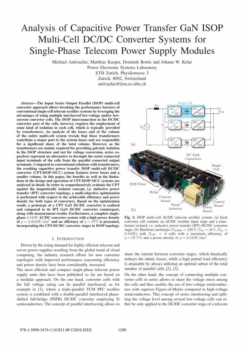
Fig. 1: ISOP multi-cell AC/DC telecom rectifier system: (a) Eachconverter cell contains an AC/DC rectifier input stage and a trans-former isolated, i.e. inductive power transfer (IPT) DC/DC converterstage; (b) Hardware prototype (Vin,RMS = 230V, Vout = 48V, Psys =3.3 kW) with Ncells = 6 cells with a maximum efficiency ofη = 97.7% and a power density of ρ = 2.2 kW/dm3.
share the current between converter stages, which drastically
reduces the ohmic losses, while a high partial load efficiency
is attainable by always utilizing an optimal subset of the total
number of parallel cells [2], [3].
On the other hand, the concept of connecting multiple con-
verter cells in series allows to share the voltage stress among
the cells and thus enables the use of low-voltage semiconduc-
tors with superior Figure-of-Merits compared to high-voltage
semiconductors. This concept of series interleaving and split-
ting the voltage level among several low-voltage cells can ei-
ther be only applied to the DC/DC converter stage of a telecom
978-1-5090-3474-1/16/$31.00 ©2016 IEEE 1280
power supply (comprising a front-end PFC rectifier and an
isolated DC/DC converter output stage [4]), or to the full con-
verter system [5] as shown in Fig. 1(a) with a series connection
of the cell’s input terminals and a parallel connection of the
output terminals (denominated as ISOP, i.e. input series output
parallel arrangement, in the following). The latter fully mod-
ular and/or cellular structure facilitates a highly efficient and
very compact system design (η = 97.7 %, ρ = 2.2 kW/dm3,
Vin,RMS = 230 V, Vout = 48 V, Psys = 3.3 kW) also for
employing only low-voltage Si semiconductors (cf. Fig. 1(b)).In this system, each converter cell comprises an AC/DC
rectifier input stage, which is a full-bridge operated with
totem-pole modulation (i.e. one bridge leg operates with PWM
and the other bridge leg switches with fundamental frequency),
and an isolated DC/DC converter output stage realized as
transformer isolated, i.e. inductive power transfer (IPT), phase-
shifted full-bridge (PSFB) converter (cf. Fig. 2(a)) which
is denominated as IPT-PSFB in the following. In [6] it is
shown, that the ISOP converter approach provides significant
benefits in terms of reduced conduction and switching losses
and smaller volumes of inductive components and heat sinks.
However, the analysis of the volume and loss distribution
of the system shown in Fig. 1(b) reveals, that the majority
of the losses is contributed by the DC/DC converter stages,
where almost half of the losses in the DC/DC converters are
resulting from the transformers. Furthermore, the transformers
represent a significant part (60%) of the total volume of the
DC/DC converter stages. The transformers have turns ratios
of N1/N2 = 1 : 1 and thus are not required for stepping
the cell DC-link voltage up or down but solely for providing
the galvanic isolation between the parallel connected outputs
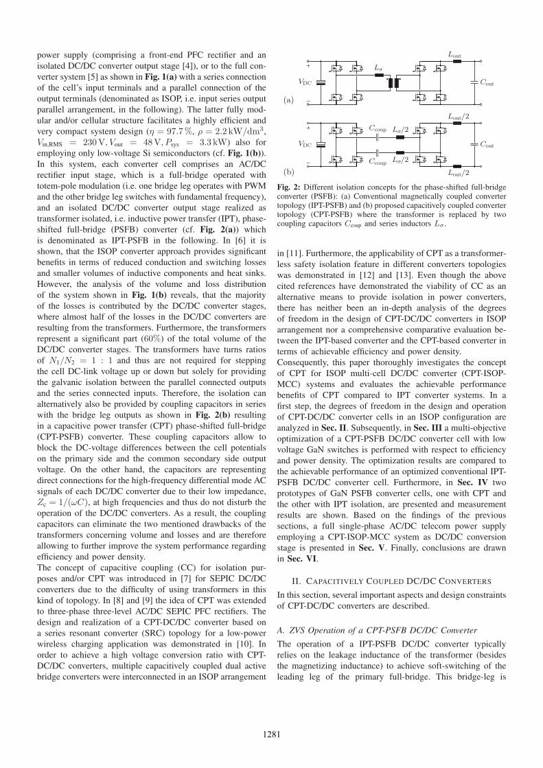
and the series connected inputs. Therefore, the isolation can
alternatively also be provided by coupling capacitors in series
with the bridge leg outputs as shown in Fig. 2(b) resulting
in a capacitive power transfer (CPT) phase-shifted full-bridge
(CPT-PSFB) converter. These coupling capacitors allow to
block the DC-voltage differences between the cell potentials
on the primary side and the common secondary side output
voltage. On the other hand, the capacitors are representing
direct connections for the high-frequency differential mode AC
signals of each DC/DC converter due to their low impedance,
Zc = 1/(ωC), at high frequencies and thus do not disturb the
operation of the DC/DC converters. As a result, the coupling
capacitors can eliminate the two mentioned drawbacks of the
transformers concerning volume and losses and are therefore
allowing to further improve the system performance regarding
efficiency and power density.
The concept of capacitive coupling (CC) for isolation pur-
poses and/or CPT was introduced in [7] for SEPIC DC/DC
converters due to the difficulty of using transformers in this
kind of topology. In [8] and [9] the idea of CPT was extended
to three-phase three-level AC/DC SEPIC PFC rectifiers. The
design and realization of a CPT-DC/DC converter based on
a series resonant converter (SRC) topology for a low-power
wireless charging application was demonstrated in [10]. In
order to achieve a high voltage conversion ratio with CPT-
DC/DC converters, multiple capacitively coupled dual active
bridge converters were interconnected in an ISOP arrangement
Ccoup
Ccoup
Lout/2
Cout
Lσ/2
VDC
Lσ/2
Lout/2
Lout
Cout
Lσ
VDC
(a)
(b)
Fig. 2: Different isolation concepts for the phase-shifted full-bridgeconverter (PSFB): (a) Conventional magnetically coupled convertertopology (IPT-PSFB) and (b) proposed capacitively coupled convertertopology (CPT-PSFB) where the transformer is replaced by twocoupling capacitors Ccoup and series inductors Lσ .
in [11]. Furthermore, the applicability of CPT as a transformer-
less safety isolation feature in different converters topologies
was demonstrated in [12] and [13]. Even though the above
cited references have demonstrated the viability of CC as an
alternative means to provide isolation in power converters,
there has neither been an in-depth analysis of the degrees
of freedom in the design of CPT-DC/DC converters in ISOP
arrangement nor a comprehensive comparative evaluation be-
tween the IPT-based converter and the CPT-based converter in
terms of achievable efficiency and power density.
Consequently, this paper thoroughly investigates the concept
of CPT for ISOP multi-cell DC/DC converter (CPT-ISOP-
MCC) systems and evaluates the achievable performance
benefits of CPT compared to IPT converter systems. In a
first step, the degrees of freedom in the design and operation
of CPT-DC/DC converter cells in an ISOP configuration are
analyzed in Sec. II. Subsequently, in Sec. III a multi-objective
optimization of a CPT-PSFB DC/DC converter cell with low
voltage GaN switches is performed with respect to efficiency
and power density. The optimization results are compared to
the achievable performance of an optimized conventional IPT-
PSFB DC/DC converter cell. Furthermore, in Sec. IV two
prototypes of GaN PSFB converter cells, one with CPT and
the other with IPT isolation, are presented and measurement
results are shown. Based on the findings of the previous
sections, a full single-phase AC/DC telecom power supply
employing a CPT-ISOP-MCC system as DC/DC conversion
stage is presented in Sec. V. Finally, conclusions are drawn
in Sec. VI.
II. CAPACITIVELY COUPLED DC/DC CONVERTERS
In this section, several important aspects and design constraints
of CPT-DC/DC converters are described.
A. ZVS Operation of a CPT-PSFB DC/DC Converter
The operation of a IPT-PSFB DC/DC converter typically
relies on the leakage inductance of the transformer (besides
the magnetizing inductance) to achieve soft-switching of the
leading leg of the primary full-bridge. This bridge-leg is
1281
always switched after the freewheeling phase where only
the leakage inductance drives the switching transition. The
condition for a complete soft-switching process depends on the
stored energy in the leakage inductance, the stored charge in
the parasitic output capacitance of the switches of the bridge-
leg and the DC-link voltage [14]. Since the transformer is
omitted in the CPT-PSFB concept, a dedicated inductor has to
be added in series with the coupling capacitors for ensuring
soft-switching. This inductor basically resembles the former
leakage inductance of the transformer.
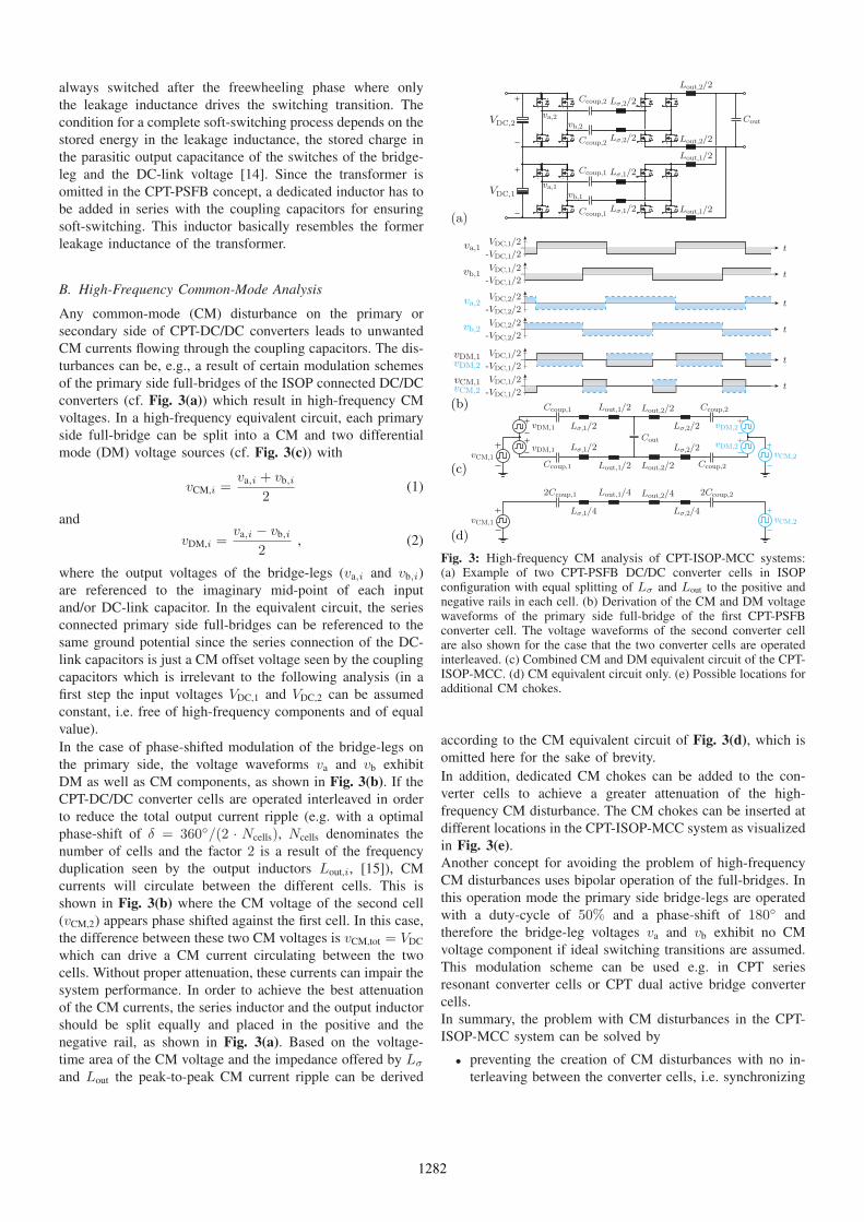
B. High-Frequency Common-Mode Analysis
Any common-mode (CM) disturbance on the primary or
secondary side of CPT-DC/DC converters leads to unwanted
CM currents flowing through the coupling capacitors. The dis-
turbances can be, e.g., a result of certain modulation schemes
of the primary side full-bridges of the ISOP connected DC/DC
converters (cf. Fig. 3(a)) which result in high-frequency CM
voltages. In a high-frequency equivalent circuit, each primary
side full-bridge can be split into a CM and two differential
mode (DM) voltage sources (cf. Fig. 3(c)) with
vCM,i =va,i + vb,i
2(1)
and
vDM,i =va,i − vb,i
2, (2)
where the output voltages of the bridge-legs (va,i and vb,i)
are referenced to the imaginary mid-point of each input
and/or DC-link capacitor. In the equivalent circuit, the series
connected primary side full-bridges can be referenced to the
same ground potential since the series connection of the DC-
link capacitors is just a CM offset voltage seen by the coupling
capacitors which is irrelevant to the following analysis (in a
first step the input voltages VDC,1 and VDC,2 can be assumed
constant, i.e. free of high-frequency components and of equal
value).
In the case of phase-shifted modulation of the bridge-legs on
the primary side, the voltage waveforms va and vb exhibit
DM as well as CM components, as shown in Fig. 3(b). If the
CPT-DC/DC converter cells are operated interleaved in order
to reduce the total output current ripple (e.g. with a optimal
phase-shift of δ = 360◦/(2 · Ncells), Ncells denominates the
number of cells and the factor 2 is a result of the frequency
duplication seen by the output inductors Lout,i, [15]), CM
currents will circulate between the different cells. This is
shown in Fig. 3(b) where the CM voltage of the second cell
(vCM,2) appears phase shifted against the first cell. In this case,
the difference between these two CM voltages is vCM,tot = VDC
which can drive a CM current circulating between the two
cells. Without proper attenuation, these currents can impair the
system performance. In order to achieve the best attenuation
of the CM currents, the series inductor and the output inductor
should be split equally and placed in the positive and the
negative rail, as shown in Fig. 3(a). Based on the voltage-
time area of the CM voltage and the impedance offered by Lσ
and Lout the peak-to-peak CM current ripple can be derived
DC,2V
DC,1Vva,1
vb,1
va,2vb,2
Ccoup,2
Ccoup,1 Lσ,1/2
Ccoup,1
Ccoup,2
Lout,2/2
vCM,1
vDM,1
vDM,1
Cout
Cout
vDM,2
vDM,2vCM,2
Ccoup,1
Ccoup,1
Ccoup,2
Ccoup,2
Lout,2/2
Lout,1/2
Lout,1/2Lσ,1/2
Lσ,2/2
Lσ,2/2
Lσ,1/2
Lout,1/2
Lσ,1/2
Lout,1/2
Lout,2/2
Lout,2/2
Lσ,2/2
Lσ,2/2
vCM,1 vCM,2
2Ccoup,1 2Ccoup,2
Lσ,1/4
Lout,1/4 Lout,2/4
Lσ,2/4
(c)
(a)
(d)
va,1VDC,1/2
-VDC,1/2t
vb,1VDC,1/2
-VDC,1/2t
va,2VDC,2/2
-VDC,2/2t
vb,2VDC,2/2
-VDC,2/2t
vCM,1 VDC,1/2
-VDC,1/2t
vDM,1 t
(b)
vCM,2
VDC,1/2
-VDC,1/2vDM,2
Fig. 3: High-frequency CM analysis of CPT-ISOP-MCC systems:(a) Example of two CPT-PSFB DC/DC converter cells in ISOPconfiguration with equal splitting of Lσ and Lout to the positive andnegative rails in each cell. (b) Derivation of the CM and DM voltagewaveforms of the primary side full-bridge of the first CPT-PSFBconverter cell. The voltage waveforms of the second converter cellare also shown for the case that the two converter cells are operatedinterleaved. (c) Combined CM and DM equivalent circuit of the CPT-ISOP-MCC. (d) CM equivalent circuit only. (e) Possible locations foradditional CM chokes.
according to the CM equivalent circuit of Fig. 3(d), which is
omitted here for the sake of brevity.
In addition, dedicated CM chokes can be added to the con-
verter cells to achieve a greater attenuation of the high-
frequency CM disturbance. The CM chokes can be inserted at
different locations in the CPT-ISOP-MCC system as visualized
in Fig. 3(e).Another concept for avoiding the problem of high-frequency
CM disturbances uses bipolar operation of the full-bridges. In
this operation mode the primary side bridge-legs are operated
with a duty-cycle of 50% and a phase-shift of 180◦ and
therefore the bridge-leg voltages va and vb exhibit no CM
voltage component if ideal switching transitions are assumed.
This modulation scheme can be used e.g. in CPT series
resonant converter cells or CPT dual active bridge converter
cells.
In summary, the problem with CM disturbances in the CPT-
ISOP-MCC system can be solved by
• preventing the creation of CM disturbances with no in-
terleaving between the converter cells, i.e. synchronizing
1282
DC
DC
DC
DC
DC
DCvDC,1
vDC,N
vDC,2
DC
DCvDC,3
VDC,1
Ccm,1
vcm,1
vcm,2
vcm,3
vcm,N
Ccm,2
Ccm,3
Ccm,N
vac,1vDC,1
VDC,2
vac,2vDC,2
2vDC,1
2vDC,2
2vDC,3
2vDC,N
Fig. 4: Low-frequency CM equivalent circuit (right) of the CPT-ISOP-MCC system (left). (The output voltage is assumed constant,i.e. free of low-frequency as result of the output voltage control. Fur-thermore, the negative output terminal is considered to be connectedto ground.) This equivalent circuit allows to model the influenceof voltage fluctuations on the DC-link voltages vDC,i. Due to thelow frequency of the disturbance, the impedance of the CM path ineach cell is dominated by the coupling capacitors whereas the seriesinductance and the output inductance can be neglected.
the switching patterns, or by
• employing CM chokes, if the impedance offered by the
inductors Lσ and Lout is not sufficient, or by
• using bipolar modulation, such as applicable to CPT
series resonant or CPT dual active bridge converters.
C. Selection of Coupling Capacitance Value
In order to select a suitable capacitance value for the coupling
capacitors, the lower and upper boundaries of the capacitance
values have to be derived.
For the upper boundary, the inherent power fluctuation present
in a single phase AC/DC telecom power supply with twice
the mains frequency, e.g. 100 Hz for the European mains, has
to be considered. This power fluctuation results in a voltage
ripple on the DC-link capacitors which is also present on the
coupling capacitors. The voltage ripple creates unwanted CM
currents charging/discharging the coupling capacitors and thus
additional reactive power circulation. Mathematically, the peak
voltage fluctuation ΔVtot of the total DC-link with twice the
grid frequency ωg can be derived as
ΔVtot =Psys
2ωg · CDC,tot · VDC,tot
(3)
(neglecting the energy stored in the coupling capacitors) where
Psys is the rated system output power, VDC,tot =∑Ncells
i=1 VVD,i
is the average value of the total DC-link voltage and CDC,tot
is the total DC-link capacitance (i.e. series connection of the
DC-link capacitors of all cells and any additional full voltage
capacitors of the DC-link). Under the assumption that ΔVtot is
small compared to the average DC-link voltage, the fluctuation
of the DC-link voltage can be assumed to be sinusoidal. Hence,
the input voltage of each cell can be written as sum of a DC-
component and an AC-component, i.e.
vDC,i(t) = VDC,i + vac,i(t) = VDC,i + ΔVi · sin(2ωgt) , (4)
where i ∈ [1, Ncells]. Due to the self-balancing nature of the
ISOP interconnection of the cells [15], it can be assumed that
the input voltages of all cells are equal, which means that
VDC,i = VDC = VDC,tot/Ncells and ΔVi = ΔV = ΔVtot/Ncells.
According to the low-frequency CM equivalent circuit of the
CPT-ISOP-MCC system (cf. Fig. 4), the CM voltage across the
coupling capacitors in a converter cell (i.e. Ccm,i = 2 · Ccoup)
can be written as
vcm,i =
(i − 1
2
)· VDC +
(i − 1
2
)· ΔV · sin(2ωgt) . (5)
The AC-component of vcm,i drives a current through Ccm,i
which has an RMS-value of
Icm,RMS,i =1√2·(
i − 1
2
)· VDC · 2ωg · Ccm,i. (6)
The total CM current through all coupling capacitors can thus
be obtained by summing up all individual CM currents, i.e.
Icm,RMS,tot =
Ncells∑i=1
Icm,RMS,i = N2cells ·
ΔV√2
ωg · Ccm. (7)
This value can be related to the RMS-current value of the
DC-link capacitors, given as
IDC-link,rms =ΔVtot√
2· 2ωg · CDC,tot, (8)
which yields
ki,cm =Icm,RMS,tot
IDC-link,rms
=Ncells · Ccm
2 · CDC,tot
. (9)
This equation can be solved to find the maximum allowable
CM capacitance value and thus the maximum coupling capac-
itance value (Ccm,max = 2 · Ccoup,max) for a chosen value of
ki,cm. The result of the above calculations for a system with
Ncells = 6, Psys = 3.3 kW, ωg = 2π50 Hz, VDC,tot = 400 Vand a peak voltage fluctuation of ΔV = 0.05 · VDC,tot of the
DC-link and a chosen value ki,cm = 0.2 yields a maximum
allowable capacitance value of the coupling capacitors of
Ccoup,max = 21.9μF.
On the other hand, the lower boundary for the capacitance
value of the coupling capacitors is defined by the maximum
permissible voltage ripple caused by the high-frequency DM
AC-current at full load operation. By approximating that the
DM current through the capacitors is a square wave with a
magnitude equal to the load current Iload,i impressed by the
cell output inductors (i.e. neglecting the ripple of the output
current), the charge flowing into/out of the coupling capacitors
during half a switching period is
QDM =Iload,i
2 · fsw
(10)
with fsw being the switching frequency. If the total maximum
differential mode voltage ripple at the coupling capacitors
should be limited to a fraction of the cell DC-link voltage
(i.e. ΔVDM = kv · VDC) the total DM capacitance has to be at
least
CDM,min =QDM
ΔVDM
=QDM
kv · VDC
. (11)
1283
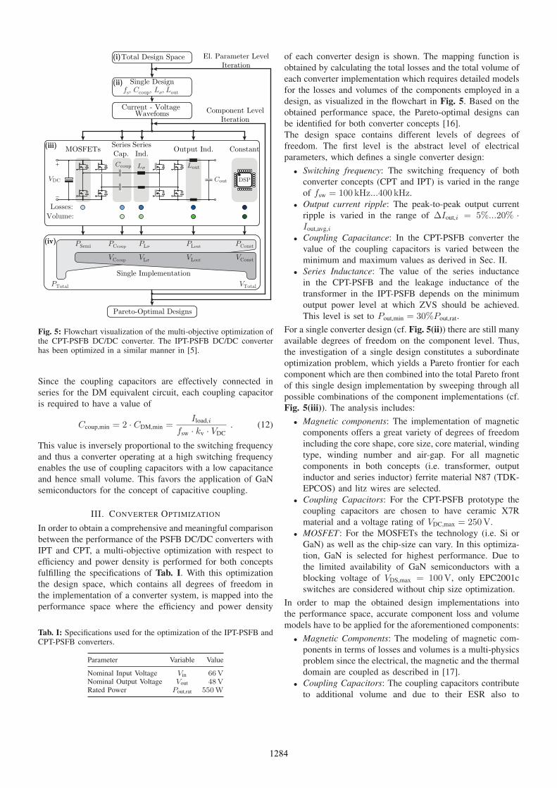
Total Design Space
Current - Voltage Wavefoms
Single Implementation
SeriesInd.
SeriesCap.
MOSFETs
(i)
(ii)
(iii)
(iv)
Output Ind. Constant
Losses:
Volume:
Ccoup Lout
Cout
Lσ
VDC DSP
PTotal VTotal
VCcoup VLσ VLout VConst
PSemi PCcoup PLσ PLout PConst
Single Designfs, Ccoup, Lσ, Lout
Pareto-Optimal Designs
El. Parameter LevelIteration
Component LevelIteration
Fig. 5: Flowchart visualization of the multi-objective optimization ofthe CPT-PSFB DC/DC converter. The IPT-PSFB DC/DC converterhas been optimized in a similar manner in [5].
Since the coupling capacitors are effectively connected in
series for the DM equivalent circuit, each coupling capacitor
is required to have a value of
Ccoup,min = 2 · CDM,min =Iload,i
fsw · kv · VDC
. (12)
This value is inversely proportional to the switching frequency
and thus a converter operating at a high switching frequency
enables the use of coupling capacitors with a low capacitance
and hence small volume. This favors the application of GaN
semiconductors for the concept of capacitive coupling.
III. CONVERTER OPTIMIZATION
In order to obtain a comprehensive and meaningful comparison
between the performance of the PSFB DC/DC converters with
IPT and CPT, a multi-objective optimization with respect to
efficiency and power density is performed for both concepts
fulfilling the specifications of Tab. I. With this optimization
the design space, which contains all degrees of freedom in
the implementation of a converter system, is mapped into the
performance space where the efficiency and power density
Tab. I: Specifications used for the optimization of the IPT-PSFB andCPT-PSFB converters.
Parameter Variable Value
Nominal Input Voltage Vin 66 VNominal Output Voltage Vout 48 VRated Power Pout,rat 550 W
of each converter design is shown. The mapping function is
obtained by calculating the total losses and the total volume of
each converter implementation which requires detailed models
for the losses and volumes of the components employed in a
design, as visualized in the flowchart in Fig. 5. Based on the
obtained performance space, the Pareto-optimal designs can
be identified for both converter concepts [16].
The design space contains different levels of degrees of
freedom. The first level is the abstract level of electrical
parameters, which defines a single converter design:
• Switching frequency: The switching frequency of both
converter concepts (CPT and IPT) is varied in the range
of fsw = 100 kHz...400 kHz.
• Output current ripple: The peak-to-peak output current
ripple is varied in the range of ΔIout,i = 5%...20% ·Iout,avg,i
• Coupling Capacitance: In the CPT-PSFB converter the
value of the coupling capacitors is varied between the
minimum and maximum values as derived in Sec. II.
• Series Inductance: The value of the series inductance
in the CPT-PSFB and the leakage inductance of the
transformer in the IPT-PSFB depends on the minimum
output power level at which ZVS should be achieved.
This level is set to Pout,min = 30%Pout,rat.
For a single converter design (cf. Fig. 5(ii)) there are still many
available degrees of freedom on the component level. Thus,
the investigation of a single design constitutes a subordinate
optimization problem, which yields a Pareto frontier for each
component which are then combined into the total Pareto front
of this single design implementation by sweeping through all
possible combinations of the component implementations (cf.
Fig. 5(iii)). The analysis includes:
• Magnetic components: The implementation of magnetic
components offers a great variety of degrees of freedom
including the core shape, core size, core material, winding
type, winding number and air-gap. For all magnetic
components in both concepts (i.e. transformer, output
inductor and series inductor) ferrite material N87 (TDK-
EPCOS) and litz wires are selected.
• Coupling Capacitors: For the CPT-PSFB prototype the
coupling capacitors are chosen to have ceramic X7R
material and a voltage rating of VDC,max = 250V.
• MOSFET: For the MOSFETs the technology (i.e. Si or
GaN) as well as the chip-size can vary. In this optimiza-
tion, GaN is selected for highest performance. Due to
the limited availability of GaN semiconductors with a
blocking voltage of VDS,max = 100 V, only EPC2001c
switches are considered without chip size optimization.
In order to map the obtained design implementations into
the performance space, accurate component loss and volume
models have to be applied for the aforementioned components:
• Magnetic Components: The modeling of magnetic com-
ponents in terms of losses and volumes is a multi-physics
problem since the electrical, the magnetic and the thermal
domain are coupled as described in [17].
• Coupling Capacitors: The coupling capacitors contribute
to additional volume and due to their ESR also to
1284
0 5 35
98.2
99.4
98.4
98
98.8
10
98.6
99
99.2
15 2520 30
ρ [kW/dm3]
η [%]
CPT-PSFBIPT-PSFBPrototype Designs
Fig. 6: η-ρ efficiency vs. power density Pareto optimization resultsof the GaN IPT-PSFB and the GaN CPT-PSFB DC/DC converter.The efficiencies are calculated for the operation at nominal voltagesand an output power level of Pout,opt = 80%Pout,rat. The powerdensity is obtained by summing up all boxed component values ofa design. Additionally, the designs are indicated which are selectedfor realization as prototypes.
conduction losses.
• MOSFETs: Due to ZVS operation of the MOSFETs only
conduction losses and gate driver losses are taken into
account.
• Constant Losses and Volumes: The losses caused by
auxiliary electronics like the DSP are approximated by
a constant loss term of Pconst = 0.4 W. The volume of
the auxiliary electronics and the PCBs are estimated to
be around Vconst = 0.01 dm3 .
By summing up the losses (calculated for an output power
level of Pout,opt = 80%Pout,rat) and volumes of all components
in each design implementation (cf. Fig. 5(iv)), and by conse-
quently iterating the process for all the designs constituting the
complete design space, the total performance space is created.
The results of this optimization process for both converter
topologies are shown in Fig. 6 with respect to efficiency (η)
and power density (ρ) of the designs.
The power density is calculated by relating the rated power
to the sum of the boxed component volumes. In a real setup,
the space between the components and mechanical constraints
will reduce the power density by a factor of 0.6...0.8. This
is especially true for the highly compact designs of the CPT-
PSFB converter (i.e. ρ ≥ 30 kW/dm3).
The electrolytic DC-link capacitors are not part of the opti-
mization since they can be regarded as part of the AC/DC
conversion stage to filter the power fluctation with twice the
mains frequency.
Nevertheless, the optimization results clearly indicate the
performance benefits offered by the concept of capacitive
coupling. For the same power density the CPT-PSFB converter
achieves an efficiency improvement of Δη = +0.4%...+0.7%compared to the conventional IPT-PSFB converter. Addi-
tionally, the CPT-PSFB converter allows to achieve power
densities which are a factor of two higher than the maximum
achievable power density of the IPT-PSFB converter.
η=98.50% ρ=7.95kW/dm3 η=99.05% ρ=11.4kW/dm3
IPT-PSFB CPT-PSFB
MOSFETs
Lout 0.31W3.31W
0.32W
Constant 0.4W0.4W
3.33W
TrafoLσ
Ccoup
0.13W0.08W
0.21W2.62W
Σ 4.23WΣ 6.64W
Σ 48.5cm3
Lout
Constant
22.7cm3
10.9cm315.6cm3
4.7cm3
10cm3
22.9cm3
10cm3
36.3cm3 TrafoLσ
Ccoup
Σ 69.2cm3
Fig. 7: Detailed break-down of the calculated losses and volumesof the components employed in the two prototype designs (i.e. IPT-PSFB and CPT-PSFB) for operation at nominal input and outputvoltages and an output power of Pout = 80%Prat = 440W.
IV. MEASUREMENT RESULTS
Based on the optimization results of the previous section,
two designs are selected (i.e. one design of the IPT-PSFB
converter and one design of the CPT-PSFB converter, cf.
Fig. 6) for experimental verification. A detailed break-down of
the losses and volumes of the two converter designs is shown
in Fig. 7. The designs for the realization as prototypes have
been selected such that they have the same output inductor
volume. Thus, the improvement in power density by removing
the transformer and replacing it with coupling capacitors and a
series inductor can directly be seen in Fig. 8(a) and (b), where
the prototypes are depicted in a side-by-side comparison. The
coupling capacitors of the CPT-PSFB converter are placed
partially also in between the control and power board. A
detailed list of the components employed in the IPT-PSFB
and CPT-PSFB GaN converter prototypes is given in Tab. II.
The efficiencies of both systems have been measured for
nominal operating voltages and different levels of output
power. The measurement results are shown for comparison
in Fig. 8(c). The PCBs in both converter prototypes have four
coppers layers with a copper thickness of tCu = 35μm each,
which leads to total resistances of the PCB conduction paths of
RPCB = 7 mΩ in both converters. The resistive losses caused
by the PCBs are subtracted in the corrected efficiency curves
of Fig. 8(c) which can be considered as upper limits for the
prototypes if thicker copper layers are chosen. But even then
the efficiency measurement results of the converter systems are
lower than the calculated efficiency values (cf. Fig. 7). One
reason for this was found to reside in the losses associated with
the charging/discharging process of the synchronous rectifica-
tion full-bridge and the attached overvoltage snubber, as used
in [6]. Furthermore, the difference between the calculations
and the measurements can also be partially explained by higher
than expected conduction losses in the GaN switches due
to suboptimal gate driver layouts which resulted from the
compromise to achieve a higher power density. This effect also
prevented measurements at elevated power levels due to the
limitations of the passive cooling concept. Nevertheless, the
1285
Transformer
OutputInductor
DC-LinkCapacitors
SeriesInductor
PowerBoard
ControlBoard(a) (b)
100 150 200 300 400
99.5
98.0
97.5
98.5
250 350
99.0
500450Pout / W
η /
%
IPT-PSFB
MeasurementCorrectionInterpolation
CPT-PSFB
(c)
Fig. 8: Experimental results: (a) Hardware demonstrator of the GaNIPT-PSFB DC/DC converter and (b) hardware demonstrator of theGaN CPT-PSFB converter. By replacing the transformer with a seriesinductor and coupling capacitors (placed in between the controland power board), the total volume of required components can bedecreased. (c) Comparison of the measured efficiency of the twoconverter prototypes. The corrected efficiency curves (shown dashed)are obtained by subtracting the resistive PCB losses and can beregarded as upper efficiency limits for the case where thicker PCBcopper layers are used.
gain in efficiency which can be achieved by the transformerless
CPT-PSFB system in contrast to the IPT-PSFB converter is
clearly recognizable.
V. FULL AC/DC TELECOM POWER SUPPLY MODULE
The superior performance of the CPT-DC/DC converters,
compared to their conventional IPT counterparts is evident
from the previous sections. However, in the context of a
Tab. II: List of employed components in the IPT-PSFB and the CPT-PSFB GaN converter prototypes.
Parameter IPT-PSFB CPT-PSFB
Switching Frequency 155 kHz 185 kHzMOSFETs (prim. & sec.) EPC2001c,
RDS,on = 7 mΩEPC2001c,RDS,on = 7 mΩ
Output Inductor Lo = 12.6μHNturns = 4RM14LP ferrite N87
Lo = 28μHNturns = 4RM14LP ferrite N87
Transformer Nprim : Nsec = 7 : 7RM14 ferrite N87
N/A
Series Inductor N/A Lo = 1μHNturns = 4E20 ferrite N87
Coupling Capacitors N/A Cs = 12μF, X7RSMD 2220, Vmax=250 V
telecom rectifier application, the AC/DC stage, which is an
indispensable part of the system, must also be incorporated in
the multi-objective optimization. Only then, tangible results
on a holistic system level can be acquired.
If the DC/DC converter stage in the telecom power supply is
realized as a CPT-ISOP-MCC, the AC/DC rectifier stage has
to provide a single DC-link voltage in order to avoid steeply
changing cell potentials as given for the fully modular/cellular
concept of Fig. 1(a). For achieving highest efficiencies of
the AC/DC rectification stage, the switching as well as the
conduction losses have to be minimized. On the one hand,
the switching losses of the high-voltage (i.e. VDS = 600 V)
switches can be reduced, if not completely eliminated, by
means of ZVS operation like with a triangular current mode
(TCM) control. On the other hand, the conduction losses
can be lowered by paralleling and/or interleaving multiple
TCM rectifier stages, such as proposed with 3 stages in [1]
for a system with η = 98.5% and ρ = 4.8 kW/dm3. The
semiconductors used in the implementation of [1] are Si
MOSFETs which can be replaced by GaN HEMTs with the
same voltage rating but lower RDS,on for the same chip area.
Furthermore, since the double-line frequency power pulsation
with the accompanying voltage ripple on the DC-link capac-
itors creates CM disturbances in the CPT-DC/DC converters,
the power pulsation can be compensated by a dedicated Power
Pulsation Buffer (PPB) [18]. This concept allows to obtain a
stable DC-link voltage without any voltage fluctuation as well
as to reduce the total size of employed DC-link capacitors. The
improvement in power-density and voltage stability, however,
is a trade-off with the efficiency of the PPB. The employed
semiconductors can also be GaN HEMTs with a voltage rating
of VDS = 600V if a buck-type PPB is used.
The analysis of high-frequency CM disturbances in the CPT-
ISOP-MCC has revealed, that topologies with bipolar modu-
lation are preferable since they create no CM voltage compo-
nent. This indicates that the CPT-DAB topology is the most
promising and suitable choice for this kind of application as
it also provides voltage controllability. By connecting at least
six CPT-DAB converter cells in ISOP connection, the DC-link
voltage of each cell is low enough to employ VDS = 100VGaN HEMTs.
The schematic of the power circuit of the full single-phase
telecom power supply incorporating all of the above mentioned
parts is depicted in Fig. 9. Based on the cited publications
and the results of this paper, a performance estimation of this
system results in a power density of ρ = 3.92 kW/dm3 and
an efficiency of η = 97%. Hence, the approach of capacitive
coupling enables a new path to achieve very high power-
densities.
As a comparison, in case the IPT-DC/DC converters are
employed, the utilization of a modular AC/DC stage is enabled
(Fig. 1(c)) which results in a more efficient but less compact
converter system (η = 98%, ρ = 2.2kW/dm3, Vin,RMS =230 V, Vout = 48V, Psys = 3.3 kW, [5]).
Thus, it can be deduced that the choice between capacitive and
magnetic coupling of the DC/DC converters and the related
consequences for the design of the AC/DC stage represents
a trade-off between efficiency and power density, with the
1286

(i) (ii) (iii) (iv)
Fig. 9: Proposed single-phase AC/DC telecom power supply modulewith a CPT-ISOP-DC/DC stage employing only GaN switches:(i) Triple interleaved high-frequency bridge-legs of the TCM PFCrectifier stage, (ii) low-frequency totem-pole bridge-leg, (iii) powerpulsation buffer for compensation of the pulsation of the input power,and (iv) CPT-ISOP-DC/DC converter stage comprising six ISOPconnected CPT-DC/DC converter cells. (Please note, that the CMand DM EMI input filters are not shown due to space constraints.)
approach of capacitive coupling potentially enabling high
power densities and the concept of magnetic coupling allowing
for high efficiencies.
VI. CONCLUSIONS
The design steps towards a highly efficient and extremely
compact ISOP-DC/DC converter system beyond the limits of
state-of-the-art systems are presented based on the concept of
CPT. This concept allows replacing the transformers of the
DC/DC converters of a conventional approach with a signif-
icantly more compact and efficient combination of coupling
capacitors and series inductors. The limitations and design
constraints associated with the approach of CPT are analyzed
in detail in this paper, including the phenomenon of circulating
CM currents in the CC-ISOP-MCC system as a result of CM
disturbances and their remedies.
In order to quantify the performance benefits of transformer-
less CPT converters against conventional IPT converters, a
comprehensive multi-objective optimization is performed for
both converter types with GaN semiconductors. From the
optimization results it can be concluded that the capacitive
coupling approach can simultaneously increase the power
density as well as the efficiency of the DC/DC converters. This
performance improvement is also verified with two DC/DC
converter cell prototypes ,i.e. an IPT-PSFB converter and a
CPT-PSFB converter with both employing low-voltage GaN
semiconductors.
Finally, the investigated CPT-ISOP-MCC system is analyzed
within the context of a complete AC/DC single-phase telecom
power supply module in combination with a triple-interleaved
TCM PFC rectifier and a PPB for compensating the double-
line frequency power pulsation. The performance achievable
with this system (ρ = 3.92 kW/dm3, η = 97%) shows that
the concept of CPT enables a new path for system designs
with exceptional power density.
REFERENCES
[1] J. W. Kolar, F. Krismer, Y. Lobsiger, J. Muehlethaler, T. Nussbaumer,and J. Minibock, “Extreme Efficiency Power Electronics,” in Proc. ofthe 7th Int. Conf. of Integrated Power Electronics Systems (CIPS), pp.1–22, 2012.
[2] S. Waffler and J. W. Kolar, “Efficiency Optimization of an AutomotiveMulti-Phase Bi-Directional DC-DC Converter,” in Proc. of 6th IEEEInternational Power Electronics and Motion Control Conference(IPEMC), pp. 566–572, 2009.
[3] M. Kasper, M. Antivachis, J. W. Kolar, and G. Deboy, “4D-Interleavingof Isolated ISOP Multi-Cell Converter Systems for Single Phase AC/DCConversion,” in Proc. of the Power Conversion and Intelligent MotionConference (PCIM), 2016.
[4] Y. Hayashi, “Approach for Highly Efficient and Ultra CompactConverters in Next Generation 380 V DC Distribution System,” inProc. of the Energy Conversion Congress and Exposition (ECCE USA),pp. 3803–3810, 2012.
[5] M. Kasper, D. Bortis, J. W. Kolar, and G. Deboy, “Hyper-Efficient(98%) and Super-Compact (3.3kW/dm3) Isolated AC/DC TelecomPower Supply Module based on Multi-Cell Converter Approach,” inProc. of the IEEE Energy Conversion Congress and Exposition (ECCEUSA), pp. 150–157, 2014.
[6] M. Kasper, C.-W. Chen, D. Bortis, J. W. Kolar, and G. Deboy,“Hardware Verification of a Hyper-Efficient (98%) and Super-Compact(2.2kW/dm3) Isolated AC/DC Telecom Power Supply Module based onMulti-Cell Converter Approach,” in Proc. of the IEEE Applied PowerElectronics Conference and Exposition (APEC), pp. 65–71, 2015.
[7] G. Barbehenn and S. Elgee, “SEPIC Converter with TransformerlessLine Isolation,” U.S. Patent 5,583,421, 1996.
[8] J. W. Kolar, “Weitbereichts-Dreiphasen-Dreipunktpulsgleichrichtersys-tem (Wide-Range Three-Phase Three-Level PWM Rectifier System),”Austrian Patent AT 404 415 B, 1996.
[9] J. W. Kolar, H. Sree, U. Drofenik, N. Mohan, and F. C. Zach, “A NovelThree-Phase Three-Switch Three-Level High Power Factor SEPIC-Type AC-to-DC Converter,” in Proc. of the Applied Power ElectronicsConference and Exposition (APEC), vol. 2, pp. 657–665, 1997.
[10] M. Kline, I. Izyumin, B. Boser, and S. Sanders, “Capacitive PowerTransfer for Contactless Charging,” in Proc. of the IEEE Applied PowerElectronics Conference and Exposition (APEC), pp. 1398–1404, 2011.
[11] F. Sarrafin-Ardbili, B. Allard, and J.-C. Crebier, “Capacitive Couplingfor High-Voltage Ratio Power Transfer in Multi-Cell Convertes basedon GaN HFETs,” in Proc. of the International Conference on IntegratedPower Electronics Systems (CIPS), 2016.
[12] S. Baurle, D. Matthews, and R. Saint-Pierre, “Method and Apparatusfor Transformerless Safety Isolation in a Power Supply,” U.S. PatentUS 2007/0 253 225 A1, 2007.
[13] S. Baurle, D. Matthews, and R. Saint-Pierre, “Transformerless SafetyIsolation in a Power Supply Using Safety Capacitors for GalvanicIsolation,” U.S. Patent 7,453,710 B2, 2008.
[14] M. Kasper, R. M. Burkart, G. Deboy, and J. W. Kolar, “ZVS of PowerMOSFETs Revisited,” IEEE Trans. Power Electron., vol. 31, no. 12, pp.8063–8067, Dec. 2016.
[15] M. Kasper, D. Bortis, and J. W. Kolar, “Scaling and Balancing ofMulti-Cell Converters,” in Proc. of the International Power ElectronicsConference (IPEC), 2014.
[16] J. W. Kolar, J. Biela, S. Waffler, T. Friedli, and U. Badstuebner,“Performance Trends and Limitations of Power Electronic Systems,” inProc. of the International Conference on Integrated Power ElectronicsSystems (CIPS), pp. 1–20, Mar. 2010.
[17] R. M. Burkart, H. Uemura, and J. W. Kolar, “Optimal Inductor Designfor 3-Phase Voltage-Source PWM Converters Considering DifferentMagnetic Materials and a Wide Switching Frequency Range,” in Proc.of the International Power Electronics Conference (IPEC), 2014.
[18] D. Neumayr, D. Bortis, and J. W. Kolar, “Ultra-Compact Power PulsationBuffer for Single-Phase DC/AC Converter Systems,” in Proc. of theIEEE International Power Electronics and Motion Control Conference(IPEMC-ECCE Asia), pp. 2732–2741, May 2016.
Powered by TCPDF (www.tcpdf.org)
1287