
Analysis and Design of Analog Integrated Circuits … · M.H. Perrott Issue #1: Headroom...
18
M.H. Perrott Analysis and Design of Analog Integrated Circuits Lecture 6 Current Mirrors Michael H. Perrott February 8, 2012 Copyright © 2012 by Michael H. Perrott All rights reserved.
Transcript of Analysis and Design of Analog Integrated Circuits … · M.H. Perrott Issue #1: Headroom...
M.H. Perrott
Analysis and Design of Analog Integrated CircuitsLecture 6
Current Mirrors
Michael H. PerrottFebruary 8, 2012
Copyright © 2012 by Michael H. PerrottAll rights reserved.
M.H. Perrott
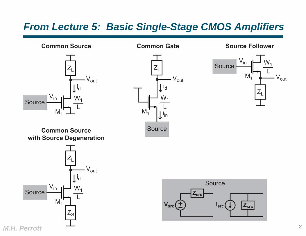
From Lecture 5: Basic Single-Stage CMOS Amplifiers
SourceM1
W1L
Vout
ZL
idVin
M1
W1L
Vout
ZL
id
iin
Source
M1
W1L
Vout
ZL
VinSource
SourceM1
W1L
Vout
ZL
idVin
ZS
Zsrc
Vsrc Isrc Zsrc
Source
Common Source Common Gate Source Follower
Common Sourcewith Source Degeneration
2
M.H. Perrott
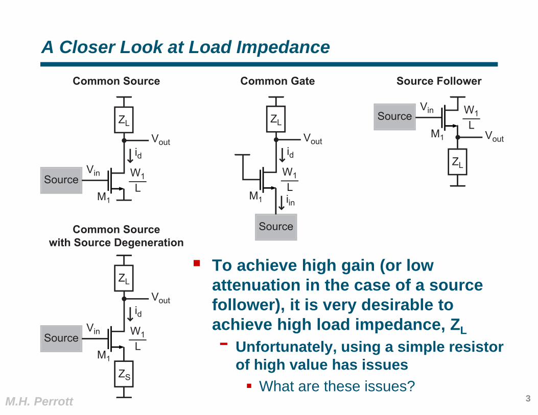
A Closer Look at Load Impedance
SourceM1
W1L
Vout
ZL
idVin
M1
W1L
Vout
ZL
id
iin
Source
M1
W1L
Vout
ZL
VinSource
SourceM1
W1L
Vout
ZL
idVin
ZS
Common Source Common Gate Source Follower
Common Sourcewith Source Degeneration
To achieve high gain (or low attenuation in the case of a source follower), it is very desirable to achieve high load impedance, ZL- Unfortunately, using a simple resistor
of high value has issues What are these issues?
3

M.H. Perrott
Issue #1: Headroom Limitations
The bias current of the device is a direct function of RL
- Vdd is < 3.6V for most modern CMOS processes- Vds must be greater than V to maintain device saturation
SourceM1
VoutId
Vin
Common Source
RL
Vdd
Want Vds > ΔV
Id =Vdd − VdsRL
Large RL implies small Id(implies small gm, poor frequency response, etc.)
4
M.H. Perrott
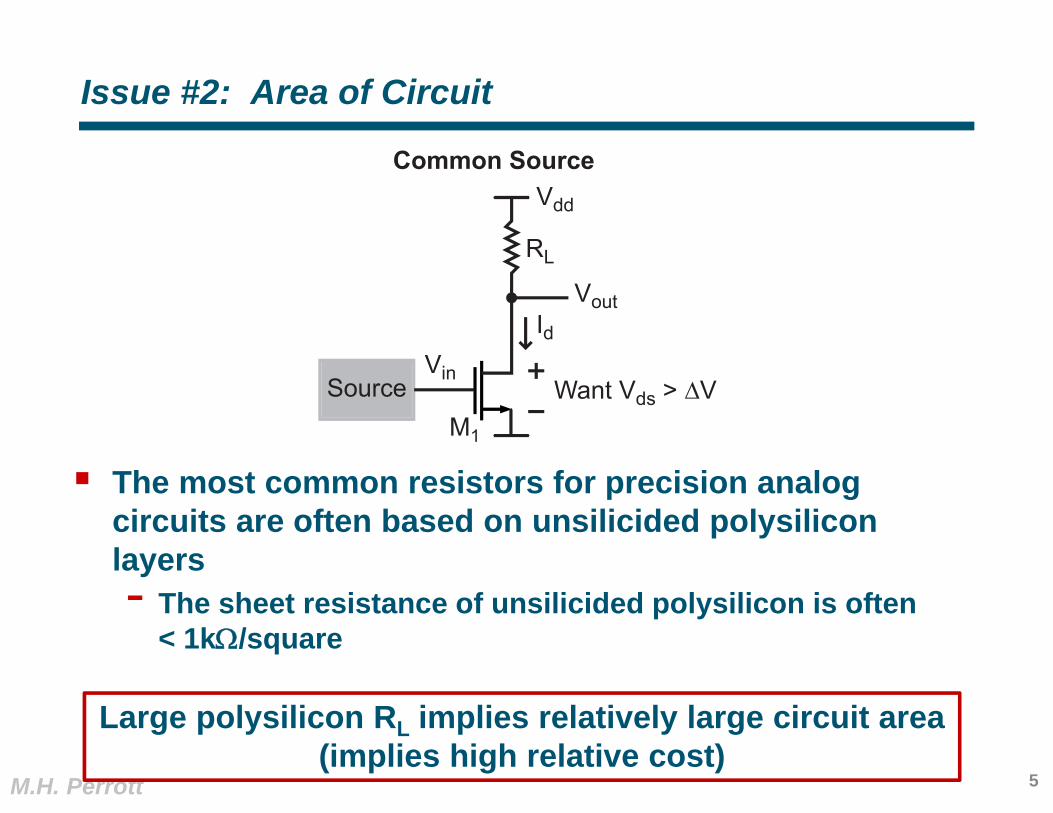
Issue #2: Area of Circuit
The most common resistors for precision analog circuits are often based on unsilicided polysiliconlayers- The sheet resistance of unsilicided polysilicon is often
< 1k/square
SourceM1
VoutId
Vin
Common Source
RL
Vdd
Want Vds > ΔV
Large polysilicon RL implies relatively large circuit area(implies high relative cost)
5

M.H. Perrott
An Elegant Approach to Achieving High Gain
Replacement of resistor load with a current source yields the highest possible DC gain out of the amplifier- Current source determines Id of device
We can make current sources out of transistors- Generally smaller area than polysilicon resistors
SourceM1
VoutId
Vin
Common SourceVdd
Vds1 > ΔV1
Ibias
What is the small signal gain of the above circuit?6

M.H. Perrott
A Simple Transistor Based Current Source
Simply use a PMOS load that is properly biased- If we keep the PMOS in saturation, its current is
relatively constant despite Vsd variations This is the desired behavior of a current source
SourceM1
VoutId
Vin
Vdd
Vds1 > ΔV1
M2
Vbias Vsd2 > ΔV2
What are the nonideal issues of the above approach?7

M.H. Perrott
Issue #1: Impedance of PMOS Device
An ideal current source has infinite impedance PMOS devices have finite impedance
- What is ZL in the above circuit?- How does finite ZL impact the gain of the circuit?
SourceM1
VoutId
Vin
Vdd
Vds1 > ΔV1
M2
Vbias Vsd2 > ΔV2
ZL
We will later examine techniques to increase ZL8

M.H. Perrott
Issue #1: High Bias Sensitivity
The PMOS device current, Id, is very sensitive to the value of Vbias- We want Id to be relatively constant across temperature
and process variations
SourceM1
VoutId
Vin
Vdd
Vds1 > ΔV1
M2
Vbias W2L
How can we achieve tighter control over Id acrosstemperature and process variations?
9

M.H. Perrott
Key Technique: Use Current Mirror
Key idea: use a different PMOS device, M3, to transform a bias current, Ibias, into bias voltage, Vbias- Vbias now yields a consistent current, Id, in M2 (assumed to
be in saturation) across temperature and process variations- Note that layout of M2 and M3 must be done properly to
achieve good device matching
SourceM1
VoutId
Vin
Vdd
Vds1 > ΔV1
M2
Vbias
M3
Ibias
W2L
W3L Vsd2 > ΔV2
How does Id relate to Ibias?10

M.H. Perrott
NMOS Devices Can Also Be Used for Current Mirrors
We often use both NMOS and PMOS versions in designs- We’ll explore this issue further later in the semester
General issue: current mirrors involve direct feedback between drain and gate
M1
Id
VbiasVds1 > ΔV1
W1L
M2
W2L
Ibias
Zo
Can we apply proposed Thevenin modelingapproach to current mirrors?
11
M.H. Perrott
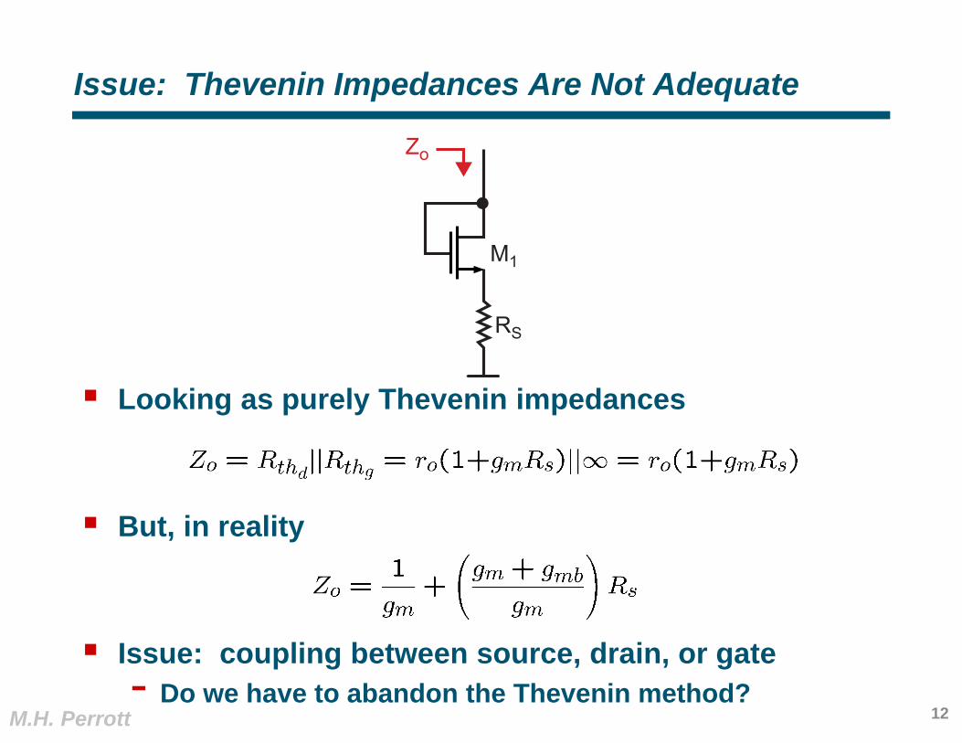
Issue: Thevenin Impedances Are Not Adequate
Looking as purely Thevenin impedances
But, in reality
Issue: coupling between source, drain, or gate- Do we have to abandon the Thevenin method?
RS
M1
Zo
12

M.H. Perrott
Try Proposed Thevenin Model
Key Calculations (ignore Rthd for now):
RthgAvvgvg
isRths
Rthdisα
g
s
d
Zo
itest vtest
Rs
13

M.H. Perrott
Proposed Thevenin Model Works!
Now include Rthd:
RthgAvvgvg
isRths
Rthdisα
g
s
d
Zo
itest vtest
Rs
14
M.H. Perrott
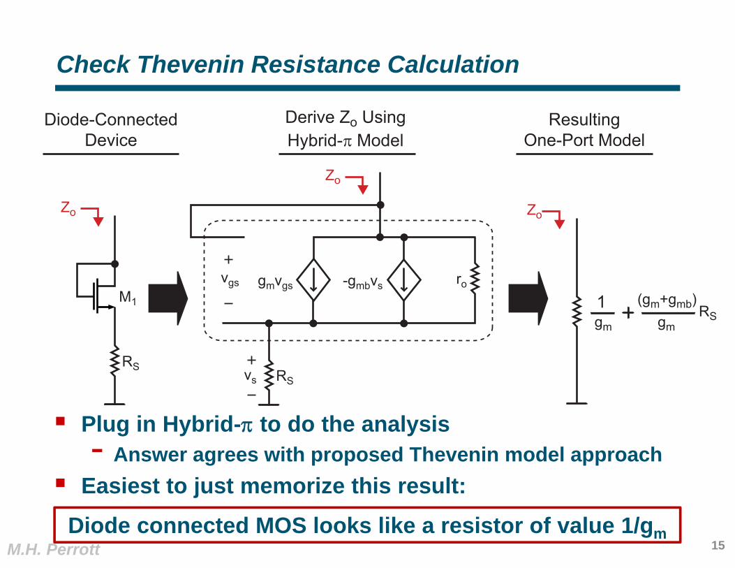
Check Thevenin Resistance Calculation
Plug in Hybrid- to do the analysis- Answer agrees with proposed Thevenin model approach
Easiest to just memorize this result:
RS
M1 (gm+gmb)gm
RS
-gmbvsvgs
vs
rogmvgs
Diode-ConnectedDevice
Derive Zo UsingHybrid-π Model
ResultingOne-Port Model
RSgm
1
Zo
Zo
Zo
Diode connected MOS looks like a resistor of value 1/gm15
M.H. Perrott
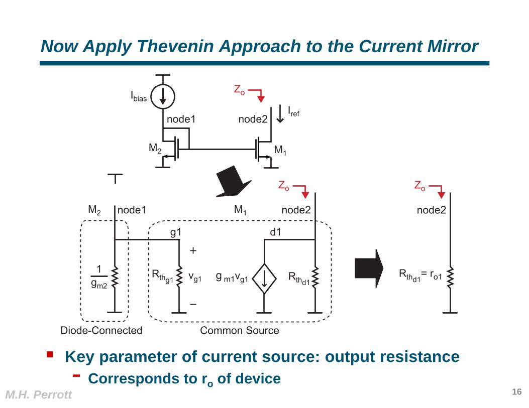
Now Apply Thevenin Approach to the Current Mirror
Key parameter of current source: output resistance- Corresponds to ro of device
M1M2
Ibias
Iref
Rthg1 vg1 Rthd1m1vg1g
g1 d1
M1
gm2
1
M2
node1 node2
node1 node2 node2
Rthd1= ro1
Common SourceDiode-Connected
Zo
Zo Zo
16
M.H. Perrott
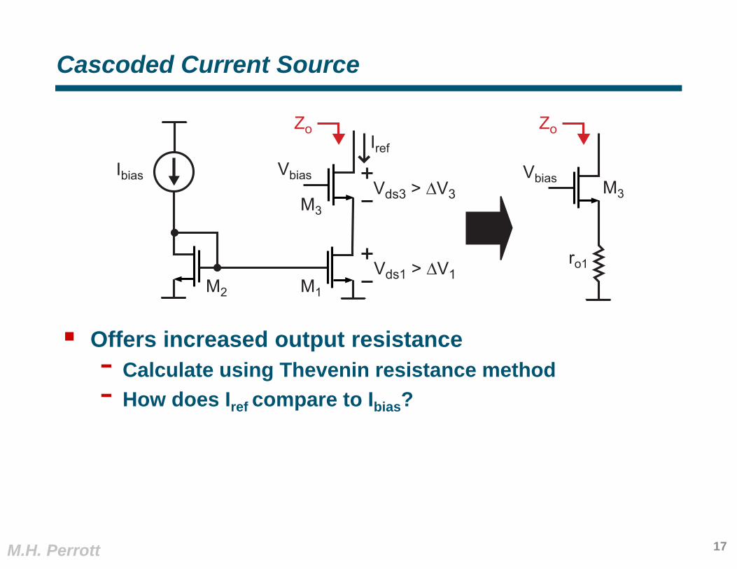
Cascoded Current Source
Offers increased output resistance- Calculate using Thevenin resistance method- How does Iref compare to Ibias?
M1M2
Ibias
Iref
ro1
M3
VbiasM3
Vbias
ZoZo
Vds1 > ΔV1
Vds3 > ΔV3
17
M.H. Perrott
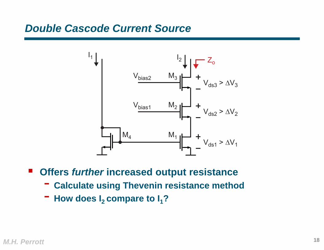
Double Cascode Current Source
Offers further increased output resistance- Calculate using Thevenin resistance method- How does I2 compare to I1?
M1
I2
M2Vbias1
M4
I1
M3Vbias2
Zo
Vds1 > ΔV1
Vds2 > ΔV2
Vds3 > ΔV3
18