Analysis and Design of Analog Front-end Circuitry for ...
137
UNLV Theses, Dissertations, Professional Papers, and Capstones 12-15-2018 Analysis and Design of Analog Front-end Circuitry for Avalanche Analysis and Design of Analog Front-end Circuitry for Avalanche Photodiodes (APD) and Silicon Photo-multipliers (SiPM) in Time- Photodiodes (APD) and Silicon Photo-multipliers (SiPM) in Time- of-flight Applications of-flight Applications Vikas Vinayaka Follow this and additional works at: https://digitalscholarship.unlv.edu/thesesdissertations Part of the Electrical and Computer Engineering Commons Repository Citation Repository Citation Vinayaka, Vikas, "Analysis and Design of Analog Front-end Circuitry for Avalanche Photodiodes (APD) and Silicon Photo-multipliers (SiPM) in Time-of-flight Applications" (2018). UNLV Theses, Dissertations, Professional Papers, and Capstones. 3460. http://dx.doi.org/10.34917/14279186 This Thesis is protected by copyright and/or related rights. It has been brought to you by Digital Scholarship@UNLV with permission from the rights-holder(s). You are free to use this Thesis in any way that is permitted by the copyright and related rights legislation that applies to your use. For other uses you need to obtain permission from the rights-holder(s) directly, unless additional rights are indicated by a Creative Commons license in the record and/ or on the work itself. This Thesis has been accepted for inclusion in UNLV Theses, Dissertations, Professional Papers, and Capstones by an authorized administrator of Digital Scholarship@UNLV. For more information, please contact [email protected].
Transcript of Analysis and Design of Analog Front-end Circuitry for ...

UNLV Theses, Dissertations, Professional Papers, and Capstones
12-15-2018
Analysis and Design of Analog Front-end Circuitry for Avalanche Analysis and Design of Analog Front-end Circuitry for Avalanche
Photodiodes (APD) and Silicon Photo-multipliers (SiPM) in Time-Photodiodes (APD) and Silicon Photo-multipliers (SiPM) in Time-
of-flight Applications of-flight Applications
Vikas Vinayaka
Follow this and additional works at: https://digitalscholarship.unlv.edu/thesesdissertations
Part of the Electrical and Computer Engineering Commons
Repository Citation Repository Citation Vinayaka, Vikas, "Analysis and Design of Analog Front-end Circuitry for Avalanche Photodiodes (APD) and Silicon Photo-multipliers (SiPM) in Time-of-flight Applications" (2018). UNLV Theses, Dissertations, Professional Papers, and Capstones. 3460. http://dx.doi.org/10.34917/14279186
This Thesis is protected by copyright and/or related rights. It has been brought to you by Digital Scholarship@UNLV with permission from the rights-holder(s). You are free to use this Thesis in any way that is permitted by the copyright and related rights legislation that applies to your use. For other uses you need to obtain permission from the rights-holder(s) directly, unless additional rights are indicated by a Creative Commons license in the record and/or on the work itself. This Thesis has been accepted for inclusion in UNLV Theses, Dissertations, Professional Papers, and Capstones by an authorized administrator of Digital Scholarship@UNLV. For more information, please contact [email protected].

ANALYSIS AND DESIGN OF ANALOG FRONT-END CIRCUITRY FOR AVALANCHE
PHOTODIODES (APD) AND SILICON PHOTO-MULTIPLIERS (SiPM) IN
TIME-OF-FLIGHT APPLICATIONS
By
Vikas Vinayaka
Bachelor of Engineering (B.E) in Electronics and Communication
Visvesvaraya Technological University, India
2010
A thesis submitted in partial fulfillment
of the requirements for the
Master of Science in Engineering - Electrical Engineering
Department of Electrical Engineering
Howard R. Hughes College of Engineering
The Graduate College
University of Nevada, Las Vegas
December 2018

c© Vikas Vinayaka, 2019
All Rights Reserved

ii
Thesis Approval
The Graduate College
The University of Nevada, Las Vegas
November 15, 2018
This thesis prepared by
Vikas Vinayaka
entitled
Analysis and Design of Analog Front-End Circuitry for Avalanche Photodiodes (APD)
and Silicon Photo-Multipliers (SiPM) in Time-of-Flight Applications
is approved in partial fulfillment of the requirements for the degree of
Master of Science in Engineering - Electrical Engineering
Department of Electrical Engineering
R. Jacob Baker, Ph.D. Kathryn Hausbeck Korgan, Ph.D. Examination Committee Chair Graduate College Interim Dean
Biswajit Das, Ph.D. Examination Committee Member
Sarah Harris, Ph.D. Examination Committee Member
Zhiyong Wang, Ph.D Graduate College Faculty Representative

Abstract
This thesis reports the analysis and design of analog front-end circuitry for reading out signals from
avalanche photodiodes (APD) or silicon photomultiplier (SiPM) in time-of-flight (ToF) applications.
An integrated circuit was designed using AMS SiGe 0.35 µm BiCMOS process. The chip measured
2 mm × 2 mm (2000 µm×2000 µm). The chip mainly contains the following circuits: an APD with
photoactive area measuring 24 µm×24 µm, an SiPM with 8×8 APDs with 236 kΩ quench resistors,
a transimpedance amplifier (TIA), a comparator and a R-2R digital to analog converter (DAC).
The TIA is based on the shunt-shunt feedback topology. The TIA gain can be digitally set using two
input bits to range from -0.9 kΩ to -14.44 kΩ with a bandwidth ranging from 93 MHz to 113 MHz.
Photodetector capacitance on TIA input reduces the bandwidth. The maximum positive input
current dynamic range of the TIA is 294 µA. The TIA consumes a power of 7.1 mW. The comparator
has a maximum speed of 265 MHz with input sensitivity down to 50 µV and consumes about
6.6 mW of power. The R-2R DAC has a 10-bit resolution with maximum differential nonlinearity
(DNL) and integral nonlinearity (INL) of -0.14 LSB and -0.09 LSB respectively with no load. Design
considerations for all the blocks are given and simulation results are compared to hand calculations.
The TIA, comparator and DAC are connected as a system and the simulation is functional. Using
this system to implement a time-of-flight LiDAR (light detection and ranging), a range resolution
down to 1.2 m (3.9 ft) can be achieved with photodetector capacitance of 0.1 pF.
iii

Acknowledgements
Sincere thanks to Dr. R. Jacob Baker for being an amazing professor, a supportive mentor and an
inspirational role model for life. I am grateful to my thesis committee members Dr. Biswajit Das,
Dr. Sarah Harris and Dr. Zhiyong Wang for their unconditional support and guidance. Thanks
to Angsuman Roy for his friendship, for providing guidance since I joined UNLV and for helping
with the thesis. Thanks to Eric Monahan for the friendship, for the personal support and for the
positive advice. Thanks to James Mellott for his warm friendship, for the technical discussions
and the encouraging words. Thanks to Sachin P Namboodiri for the friendship, for the discussions
about circuit design, for helping with the thesis and for the personal help. Thanks to Shada Sharif
for the friendship, for the positive words and key help in many occasions. Thanks to Dane Gentry,
Shadden Abdalla, Francisco Mata-carlos, Gonzalo Arteaga, James Skelly, Daniel Senda and Bryan
Kerstetter for their comradery and their efforts in my research. I have been fortunate to share my
time at UNLV with such wonderful people. Huge thanks to amma (Mother) and appaji (Father)
for everything. Thanks to Dr. Matt Pedersen for providing the LATEX template used here. Thanks
to the universe for lining up probabilities for me to achieve my goals.
Vikas Vinayaka
University of Nevada, Las Vegas
December 2018
iv

Table of Contents
Abstract iii
Acknowledgements iv
Table of Contents v
List of Tables ix
List of Figures xi
Chapter 1 Introduction 1
1.1 Organization . . . . . . . . . . . . . . . . . . . . . . . . . . . . . . . . . . . . . . . . 2
Chapter 2 Photodetectors and LiDAR 3
2.1 Photodetectors . . . . . . . . . . . . . . . . . . . . . . . . . . . . . . . . . . . . . . . 3
2.1.1 Avalanche Photodiode . . . . . . . . . . . . . . . . . . . . . . . . . . . . . . . 4
2.1.2 Silicon Photomultiplier . . . . . . . . . . . . . . . . . . . . . . . . . . . . . . . 10
2.2 LiDAR . . . . . . . . . . . . . . . . . . . . . . . . . . . . . . . . . . . . . . . . . . . . 14
2.2.1 Discrete Return LiDAR . . . . . . . . . . . . . . . . . . . . . . . . . . . . . . 15
2.2.2 Full Waveform LiDAR . . . . . . . . . . . . . . . . . . . . . . . . . . . . . . . 18
v

Chapter 3 Transimpedance Amplifier (TIA) 20
3.1 Resistor as TIA . . . . . . . . . . . . . . . . . . . . . . . . . . . . . . . . . . . . . . . 21
3.2 Feedback TIA . . . . . . . . . . . . . . . . . . . . . . . . . . . . . . . . . . . . . . . . 22
3.3 CMOS TIA . . . . . . . . . . . . . . . . . . . . . . . . . . . . . . . . . . . . . . . . . 25
3.3.1 Simulation results . . . . . . . . . . . . . . . . . . . . . . . . . . . . . . . . . 27
3.3.2 Physical layout . . . . . . . . . . . . . . . . . . . . . . . . . . . . . . . . . . . 30
3.4 Circuit analysis . . . . . . . . . . . . . . . . . . . . . . . . . . . . . . . . . . . . . . . 31
3.4.1 Switchable resistance . . . . . . . . . . . . . . . . . . . . . . . . . . . . . . . . 34
3.4.2 TIA input DC range . . . . . . . . . . . . . . . . . . . . . . . . . . . . . . . . 36
3.4.3 TIA gain . . . . . . . . . . . . . . . . . . . . . . . . . . . . . . . . . . . . . . 37
3.4.4 TIA input impedance and bandwidth . . . . . . . . . . . . . . . . . . . . . . 42
3.4.5 Source follower . . . . . . . . . . . . . . . . . . . . . . . . . . . . . . . . . . . 46
Chapter 4 Comparator 50
4.1 Simulation results . . . . . . . . . . . . . . . . . . . . . . . . . . . . . . . . . . . . . 51
4.2 Physical layout . . . . . . . . . . . . . . . . . . . . . . . . . . . . . . . . . . . . . . . 53
4.3 Analysis . . . . . . . . . . . . . . . . . . . . . . . . . . . . . . . . . . . . . . . . . . . 54
4.3.1 Preamplifier . . . . . . . . . . . . . . . . . . . . . . . . . . . . . . . . . . . . . 55
4.3.2 Sense amplifier and latch . . . . . . . . . . . . . . . . . . . . . . . . . . . . . 64
Chapter 5 R-2R Digital-to-Analog Converter (DAC) 73
5.1 Ideal DAC . . . . . . . . . . . . . . . . . . . . . . . . . . . . . . . . . . . . . . . . . . 74
5.2 DAC Linearity . . . . . . . . . . . . . . . . . . . . . . . . . . . . . . . . . . . . . . . 75
5.2.1 DNL . . . . . . . . . . . . . . . . . . . . . . . . . . . . . . . . . . . . . . . . . 75
5.2.2 INL . . . . . . . . . . . . . . . . . . . . . . . . . . . . . . . . . . . . . . . . . 76
vi

5.2.3 Gain Error . . . . . . . . . . . . . . . . . . . . . . . . . . . . . . . . . . . . . 78
5.2.4 Offset Error . . . . . . . . . . . . . . . . . . . . . . . . . . . . . . . . . . . . . 78
5.3 R-2R DAC . . . . . . . . . . . . . . . . . . . . . . . . . . . . . . . . . . . . . . . . . 79
5.3.1 Basic voltage-mode R-2R DAC . . . . . . . . . . . . . . . . . . . . . . . . . . 79
5.3.2 Current-mode operation . . . . . . . . . . . . . . . . . . . . . . . . . . . . . . 81
5.3.3 R-2R DAC schematic . . . . . . . . . . . . . . . . . . . . . . . . . . . . . . . 82
5.3.4 Simulation results . . . . . . . . . . . . . . . . . . . . . . . . . . . . . . . . . 83
5.3.5 Physical Layout . . . . . . . . . . . . . . . . . . . . . . . . . . . . . . . . . . 86
5.4 Implementation details . . . . . . . . . . . . . . . . . . . . . . . . . . . . . . . . . . . 87
5.4.1 Variable output range . . . . . . . . . . . . . . . . . . . . . . . . . . . . . . . 87
5.4.2 Serial Digital Input . . . . . . . . . . . . . . . . . . . . . . . . . . . . . . . . . 89
5.4.3 Resistive load . . . . . . . . . . . . . . . . . . . . . . . . . . . . . . . . . . . . 92
5.4.4 Effect of switch resistance . . . . . . . . . . . . . . . . . . . . . . . . . . . . . 94
5.4.5 Resistor mismatch . . . . . . . . . . . . . . . . . . . . . . . . . . . . . . . . . 95
Chapter 6 System simulations 97
6.1 LiDAR range resolution . . . . . . . . . . . . . . . . . . . . . . . . . . . . . . . . . . 100
6.2 DAC output voltage error . . . . . . . . . . . . . . . . . . . . . . . . . . . . . . . . . 102
Chapter 7 Integrated Circuit Layout 104
Chapter 8 Future Improvements and Conclusion 107
8.1 Transimpedance amplifier . . . . . . . . . . . . . . . . . . . . . . . . . . . . . . . . . 107
8.2 Comparator . . . . . . . . . . . . . . . . . . . . . . . . . . . . . . . . . . . . . . . . . 108
8.3 R-2R Digital-to-Analog Converter . . . . . . . . . . . . . . . . . . . . . . . . . . . . 108
8.4 Conclusion . . . . . . . . . . . . . . . . . . . . . . . . . . . . . . . . . . . . . . . . . 110
vii

Appendix A Script for R-2R DAC analysis 111
Bibliography 119
Curriculum Vitae 121
viii

List of Tables
2.1 Calculating the breakdown voltage of APD in AMS SiGe 0.35 µm BiCMOS process . . 9
2.2 Maximum SiPM current using APDs with Rquench = 236 kΩ in AMS SiGe 0.35 µm
BiCMOS process . . . . . . . . . . . . . . . . . . . . . . . . . . . . . . . . . . . . . . . . 13
3.1 Resistance values corresponding to input values of digital bits . . . . . . . . . . . . . . . 28
3.2 Power dissipation of TIA at different gain settings . . . . . . . . . . . . . . . . . . . . . 30
3.3 Transmission gate resistance . . . . . . . . . . . . . . . . . . . . . . . . . . . . . . . . . . 36
3.4 Input DC current range for linear gain to within 10% of maximum gain . . . . . . . . . 37
3.5 TIA gain for different gain settings . . . . . . . . . . . . . . . . . . . . . . . . . . . . . . 38
3.6 Calculated and simulated open loop gain of TIA first stage . . . . . . . . . . . . . . . . 41
3.7 Calculated and simulated closed loop gain of TIA first stage . . . . . . . . . . . . . . . . 42
3.8 Closed-loop input impedance, Rinf of TIA . . . . . . . . . . . . . . . . . . . . . . . . . . 43
3.9 Calculated bandwidth due to input pole at different values of Cin for all values of RF . 45
3.10 Simulated characteristics of TIA with varying Cin for RF=2kΩ . . . . . . . . . . . . . . 46
3.11 Simulated characteristics of TIA with varying Cin for RF=4kΩ . . . . . . . . . . . . . . 46
3.12 Simulated characteristics of TIA with varying Cin for RF=8kΩ . . . . . . . . . . . . . . 47
3.13 Simulated characteristics of TIA with varying Cin for RF=16kΩ . . . . . . . . . . . . . 47
4.1 Power consumption of comparator at different input common-mode voltages . . . . . . . 52
ix

4.2 Output common-mode voltage, collector and base currents for preamplifier single stage
at different input common-mode voltages . . . . . . . . . . . . . . . . . . . . . . . . . . 59
4.3 Preamplifier single stage gain at different input common-mode voltages . . . . . . . . . 62
4.4 Total gain of preamplifier . . . . . . . . . . . . . . . . . . . . . . . . . . . . . . . . . . . 63
4.5 Characteristic table of sense amplifier . . . . . . . . . . . . . . . . . . . . . . . . . . . . 65
4.6 Delay of sense amplifier and latch for input common-mode voltage of 4.71 V from the
preamplifier . . . . . . . . . . . . . . . . . . . . . . . . . . . . . . . . . . . . . . . . . . . 70
4.7 Truth table of 2-input NAND gate . . . . . . . . . . . . . . . . . . . . . . . . . . . . . . 72
4.8 Characteristic table of SR latch . . . . . . . . . . . . . . . . . . . . . . . . . . . . . . . . 72
5.1 Truth table of AND gate . . . . . . . . . . . . . . . . . . . . . . . . . . . . . . . . . . . 92
5.2 DAC DC nonlinearities for different load resistances . . . . . . . . . . . . . . . . . . . . 93
6.1 Comparator preamplifier and sense amplifier delays . . . . . . . . . . . . . . . . . . . . . 101
6.2 Settling time and range resolution for TIA with RF = 2kΩ . . . . . . . . . . . . . . . . 102
6.3 Settling time and range resolution for TIA with RF = 4kΩ . . . . . . . . . . . . . . . . 102
6.4 Settling time and range resolution for TIA with RF = 8kΩ . . . . . . . . . . . . . . . . 102
6.5 Settling time and range resolution for TIA with RF = 16kΩ . . . . . . . . . . . . . . . . 102
6.6 DAC output voltage error . . . . . . . . . . . . . . . . . . . . . . . . . . . . . . . . . . . 103
8.1 Slope of output voltage for change in switch resistance . . . . . . . . . . . . . . . . . . . 109
x

List of Figures
2.1 Schematic and simple electrical model of APD in Geiger-mode . . . . . . . . . . . . . . 7
2.2 Waveform of output current from APD when triggered in Geiger-mode operation . . . . 7
2.3 Cross sectional view of layers of APD fabricated in AMS SiGe 0.35 µm BiCMOS process 8
2.4 Measured output current from APD in Geiger-mode operation. Applied Vbias = 11.5 V
with Rquench = 210 kΩ . . . . . . . . . . . . . . . . . . . . . . . . . . . . . . . . . . . . . 10
2.5 Output pulse rate vs incident pulse rate of SiPM and APD. Adapted from [1] . . . . . . 11
2.6 Schematic and simple electrical model of SiPM . . . . . . . . . . . . . . . . . . . . . . . 11
2.7 Layout of SiPM . . . . . . . . . . . . . . . . . . . . . . . . . . . . . . . . . . . . . . . . . 12
2.8 Block diagram of discrete return LiDAR . . . . . . . . . . . . . . . . . . . . . . . . . . . 16
2.9 Return waveform from the discrete return LiDAR . . . . . . . . . . . . . . . . . . . . . 17
2.10 Block diagram of full waveform LiDAR . . . . . . . . . . . . . . . . . . . . . . . . . . . 19
2.11 Full waveform LiDAR return signal waveform . . . . . . . . . . . . . . . . . . . . . . . . 19
3.1 Resistor as TIA . . . . . . . . . . . . . . . . . . . . . . . . . . . . . . . . . . . . . . . . . 21
3.2 Basic block diagram of feedback TIA . . . . . . . . . . . . . . . . . . . . . . . . . . . . . 23
3.3 Feedback TIA using opamp . . . . . . . . . . . . . . . . . . . . . . . . . . . . . . . . . . 24
3.4 Feedback TIA using CMOS inverter . . . . . . . . . . . . . . . . . . . . . . . . . . . . . 24
3.5 Circuit of implemented transimpedance amplifier . . . . . . . . . . . . . . . . . . . . . . 26
xi

3.6 Circuit of switchable resistance . . . . . . . . . . . . . . . . . . . . . . . . . . . . . . . . 27
3.7 Output voltages for different gain settings with swept input current . . . . . . . . . . . 28
3.8 Slope (gain) of output voltages in Figure 3.7 . . . . . . . . . . . . . . . . . . . . . . . . 28
3.9 Transient output voltage for different gain settings . . . . . . . . . . . . . . . . . . . . . 29
3.10 Measuring settling time . . . . . . . . . . . . . . . . . . . . . . . . . . . . . . . . . . . . 29
3.11 Small-signal AC simulation showing output voltage . . . . . . . . . . . . . . . . . . . . . 30
3.12 Physical layout of CMOS TIA . . . . . . . . . . . . . . . . . . . . . . . . . . . . . . . . 31
3.13 Transmission gate circuit . . . . . . . . . . . . . . . . . . . . . . . . . . . . . . . . . . . 35
3.14 Resistance of transmission gate used to switch feedback resistors . . . . . . . . . . . . . 36
3.15 Schematic for open loop gain simulation of TIA first stage . . . . . . . . . . . . . . . . . 39
3.16 Schematic for small signal open loop gain analysis . . . . . . . . . . . . . . . . . . . . . 40
3.17 Schematic of source follower . . . . . . . . . . . . . . . . . . . . . . . . . . . . . . . . . . 48
4.1 Block diagram of comparator . . . . . . . . . . . . . . . . . . . . . . . . . . . . . . . . . 51
4.2 Preamplifier . . . . . . . . . . . . . . . . . . . . . . . . . . . . . . . . . . . . . . . . . . . 51
4.3 Sense amplifier and latch . . . . . . . . . . . . . . . . . . . . . . . . . . . . . . . . . . . 52
4.4 Transient simulation results of comparator . . . . . . . . . . . . . . . . . . . . . . . . . . 53
4.5 Physical layout of comparator . . . . . . . . . . . . . . . . . . . . . . . . . . . . . . . . . 54
4.6 Comparator waveforms. Time intervals not to scale . . . . . . . . . . . . . . . . . . . . . 54
4.7 Unit stage of preamplifier . . . . . . . . . . . . . . . . . . . . . . . . . . . . . . . . . . . 56
4.8 Simulation of output common-mode voltage vs input common-mode voltage for pream-
plifier . . . . . . . . . . . . . . . . . . . . . . . . . . . . . . . . . . . . . . . . . . . . . . 60
4.9 Calculation of output common-mode voltage vs input common-mode voltage for pream-
plifier . . . . . . . . . . . . . . . . . . . . . . . . . . . . . . . . . . . . . . . . . . . . . . 60
4.10 Equivalent circuit for gain calculations . . . . . . . . . . . . . . . . . . . . . . . . . . . . 61
xii

4.11 Plot of preamplifier delay for different values of input common-mode voltage. X-axis is
in mV . . . . . . . . . . . . . . . . . . . . . . . . . . . . . . . . . . . . . . . . . . . . . . 64
4.12 Sense amplifier . . . . . . . . . . . . . . . . . . . . . . . . . . . . . . . . . . . . . . . . . 65
4.13 Plot of sense amplifier and latch delay vs input differential voltage. X-axis is in mV . . 67
4.14 Pull-down circuit of one half of sense amplifier . . . . . . . . . . . . . . . . . . . . . . . 68
4.15 Derivative of pull-down current versus input voltage(∂iPD∂vIN
= Transconductance)
of the
circuit in Figure 4.14 . . . . . . . . . . . . . . . . . . . . . . . . . . . . . . . . . . . . . . 68
4.16 Schematic of SR latch . . . . . . . . . . . . . . . . . . . . . . . . . . . . . . . . . . . . . 71
4.17 Schematic of 2-input NAND gate used in SR latch. All PMOS = 5µm/0.5µm. All
NMOS = 4µm/0.5µm . . . . . . . . . . . . . . . . . . . . . . . . . . . . . . . . . . . . . 71
5.1 Ideal DAC characteristics for 3-bit DAC . . . . . . . . . . . . . . . . . . . . . . . . . . . 75
5.2 Measuring DAC DNL . . . . . . . . . . . . . . . . . . . . . . . . . . . . . . . . . . . . . 76
5.3 Measuring DAC INL . . . . . . . . . . . . . . . . . . . . . . . . . . . . . . . . . . . . . . 77
5.4 Gain error of DAC . . . . . . . . . . . . . . . . . . . . . . . . . . . . . . . . . . . . . . . 78
5.5 Offset error of DAC . . . . . . . . . . . . . . . . . . . . . . . . . . . . . . . . . . . . . . 79
5.6 Basic voltage-mode R-2R DAC . . . . . . . . . . . . . . . . . . . . . . . . . . . . . . . . 80
5.7 R-2R DAC operation in current-mode . . . . . . . . . . . . . . . . . . . . . . . . . . . . 81
5.8 Complete schematic of R-2R DAC . . . . . . . . . . . . . . . . . . . . . . . . . . . . . . 82
5.9 Output of DAC for input digital ramp . . . . . . . . . . . . . . . . . . . . . . . . . . . . 84
5.10 Output of DAC configured in current-mode for input digital ramp . . . . . . . . . . . . 84
5.11 Output of DAC with VREF+ = 4 V and VREF− = 1 V . . . . . . . . . . . . . . . . . . . 85
5.12 Output of DAC with serial input . . . . . . . . . . . . . . . . . . . . . . . . . . . . . . . 85
5.13 DNL and INL of DAC output with no load . . . . . . . . . . . . . . . . . . . . . . . . . 87
5.14 Physical layout of DAC . . . . . . . . . . . . . . . . . . . . . . . . . . . . . . . . . . . . 88
xiii

5.15 Logic inverter and drive inverter . . . . . . . . . . . . . . . . . . . . . . . . . . . . . . . 89
5.16 Positive edge triggered D flip-flop. CLK inverter PMOS = 5µm/0.5µm, NMOS =
2µm/0.5µm. Other PMOS = 3µm/0.5µm, NMOS = 1µm/0.5µm . . . . . . . . . . . . . 91
5.17 2-input AND gate. Inverter PMOS = 3µm/0.5µm, NMOS = 1µm/0.5µm. Other PMOS
= 3µm/0.5µm, NMOS = 2µm/0.5µm . . . . . . . . . . . . . . . . . . . . . . . . . . . . 91
5.18 DAC transfer characteristics for different load resistances . . . . . . . . . . . . . . . . . 93
5.19 Calculated DNL and INL of DAC using script in Appendix A with switch resistance =
10 Ω . . . . . . . . . . . . . . . . . . . . . . . . . . . . . . . . . . . . . . . . . . . . . . . 94
5.20 Resistance of PMOS and NMOS devices used in drive inverter. The devices are operating
in triode region where resistance is measured . . . . . . . . . . . . . . . . . . . . . . . . 95
6.1 Schematic of system simulation . . . . . . . . . . . . . . . . . . . . . . . . . . . . . . . . 98
6.2 Simulation results of Figure 6.1 . . . . . . . . . . . . . . . . . . . . . . . . . . . . . . . . 99
6.3 Simulation results of Figure 6.1 with 1pF capacitance on DAC output . . . . . . . . . . 99
6.4 Timing diagram of system. Time intervals not to scale . . . . . . . . . . . . . . . . . . . 100
7.1 Integrated Circuit Layout . . . . . . . . . . . . . . . . . . . . . . . . . . . . . . . . . . . 105
7.2 IC layout with decoupling capacitors and dummy fill . . . . . . . . . . . . . . . . . . . . 106
8.1 DNL and INL of DAC output with switch resistances given in Table 8.1 . . . . . . . . . 109
A.1 Reference schematic used for writing the script . . . . . . . . . . . . . . . . . . . . . . . 111
xiv

Chapter 1
Introduction
Sensing and processing light has wide ranging practical applications. The LiDAR (Light Detection
and Ranging), for example, is one of the main applications. The LiDAR has various uses in different
fields. A LiDAR works by sensing light from a target, and using the principle of time-of-flight to
calculate the distance. Time of flight (ToF), as the name suggests is the time taken for a wave to
travel a certain distance through a medium [2]. Examples of devices that use the same concept
using different type or wavelength of waves are the SONAR and RADAR.
Low level of light detection is needed for implementing long range LiDAR. The photodetectors
discussed in this thesis are the APD (Avalanche Photo Diode) and SiPM (Silicon Photo Multiplier)
which can be sensitive enough to detect single photons.
There are various circuit topologies available for the read-out of APDs and SiPMs. One such
topology is the Transimpedance amplifier (TIA) which takes the current output of the SiPM or
APD and outputs a voltage with gain.
The voltage output of the TIA needs to be detected for specific pulses which correspond to light
pulses. To detect these, a comparator is used. The comparator compares two voltage values and
outputs a binary value indicating if either input is higher or lower than the other. The output of
1

the comparator can be read out to find the specific time at which the optical pulse arrived.
This entire system can be built using separate components. However, integration is one of the
key techniques to achieve better performance in a system. This thesis integrates the photodetector,
the transimpedance amplifier, the comparator and the digital-to-analog converter on the same
monolithic integrated circuit (IC) to achieve better performance. Such an IC is also called a ROIC
(Read-Out Integrated Circuit).
The circuits are designed in the AMS SiGe 0.35 µm BiCMOS process. The design and simula-
tions were done using the cadence EDA software. Schematics and layout were done using Virtuoso
suite. Simulation using ADE and Spectre. Physical verification is done using Assura.
1.1 Organization
The photodetectors are described in Chapter 2. One of the main application of focus, LiDAR is also
discussed in this chapter. The components of the discrete return LiDAR will be implemented in
this thesis. The main components are the transimpedance amplifier (TIA), comparator and digital-
to-analog converter (DAC). These are described in detail in Chapters 3, 4 and 5 respectively.
In Chapter 6, these components are put together and simulated to demonstrate and verify the
operation of the entire system. The physical layout of all the circuits designed are integrated on a
chip. This is discussed in detail in Chapter 7. Chapter 8 summarizes and concludes the thesis with
some suggested improvements for future work.
2

Chapter 2
Photodetectors and LiDAR
This chapter describes the APD (Avalanche Photo Diode) and SiPM (Silicon Photo Multiplier)
photodetectors and one of their main applications, the LiDAR. Different types of LiDAR and their
associated block diagrams are described.
2.1 Photodetectors
Photodetectors are needed for sensing light. Photodiodes are high performance photodetectors due
to their quick response, solid state nature and low power. For detecting low amounts of light at
the single photon level, a regular photodiode might not be suitable, as the output current signal
would be too low. An amplifier can be used in conjunction with the regular photodetector but that
would result in inferior noise performance as the signal-to-noise ratio would be low due to low gain
of the photodetector. A good solution for this is a photodetector with built-in amplification. This
kind of photodetector has gain, so that a single photon striking the photodiode results in a large
output current signal.
Such photodetectors with built-in gain are photomultiplier tubes (PMTs) and avalanche photo-
diodes. The photomultiplier tube (PMT) is a vacuum tube consisting of a photocathode material
3

with electron amplification plates. When light strikes the photocathode, electrons are ejected due
to the photoelectric effect. The electrons are then accelerated towards the electron amplification
plates due to the potential difference. When they hit the plates, more electrons are ejected due
to secondary emission which are accelerated towards more plates, and this process repeats and
compounds for each plate. This process happens multiple times resulting in a large number of
output electrons for a small number of incident photons. The PMT is a good device for sensing a
very low amount of light. However, the PMT has some disadvantages. Firstly, due to the inherent
nature of its mechanism, it is susceptible to magnetic fields. Secondly, due to high voltages needed
to accelerate electrons in a vacuum, the PMT needs high voltages in hundreds of volts at a low
current. Also, PMTs are bulky in size and as it is a vacuum tube, is made of glass and is sensitive
to mechanical shock and vibration. Most of these disadvantages are mitigated by using solid state
photodetectors such as the avalanche photodiodes (APDs) which is discussed next.
2.1.1 Avalanche Photodiode
A photodiode is a PN junction that generates current when light is incident on it. When light
radiation that has enough energy is incident on the junction, it creates electron-hole pairs which
are charge carriers. These are pulled towards the terminals by the built-in or applied electric
field. This generates a current through the external circuit. The photodiode can have zero voltage
across it (photovoltaic mode) or can be reverse biased (photoconductive mode) [3]. The reverse
bias increases the depletion layer width and reduces capacitance which reduces response time.
The current produced is proportional to intensity of photons incident on the photodiode. For the
incident light to produce charge carriers in the junction, its energy must be higher than the bandgap
energy of the semiconductor material it is made of. Energy of light (electromagnetic radiation) is
given by Planck’s Equation (2.1) where E is the energy of photons in units of Joules, h is Planck’s
4

constant and ν is the frequency of radiation in units of Hertz calculated using ν = c/λ where c is
the speed of light and λ is the wavelength of light in meters.
E = h · ν (2.1)
The bandgap energy of semiconductor materials is usually expressed in units of eV (electron-volts)
which is not an SI unit and cannot be directly used in Equation (2.1). To convert units of eV to
Joules, the conversion factor is the value of electron charge. A photodiode fabricated using Silicon
which has a bandgap energy of 1.12 eV can detect wavelengths up to 1100 nm but the response
falls off sharply after 900 nm [4, p. 7]. A photodiode fabricated using Germanium which has a
bandgap energy of 0.67 eV can detect wavelengths up to 1700 nm. SiGe (Silicon-Germanium) is
a heterogeneous semiconductor which is a combination of Silicon and Germanium whose bandgap
energy can be varied depending on the ratio of silicon to germanium. As a result, SiGe has a
bandgap energy that is lower than silicon and higher than germanium. A photodiode fabricated
using SiGe can detect higher wavelengths compared to silicon photodiode.
Detecting low amounts of light at the single photon level is needed for applications such as
LiDAR described in Section 2.2. In these applications, a regular photodiode does not provide
enough output level for detection. Moreover, due to photodiode noise, the resulting signal output
would be buried in noise and have low signal-to-noise ratio.
The APD solves this issue because of its built-in gain. An APD (avalanche photo diode) is
reverse biased at a voltage close to or above its avalanche breakdown voltage. The charge carriers
generated by the photoelectric effect get multiplied due to impact ionization and the resulting
current is much larger. The gain of the APD is proportional to the applied reverse bias voltage.
An APD can be operated in linear mode or Geiger-mode. In linear mode operation, the APD
bias voltage is below the avalanche threshold. The output current is linearly proportional to the
amount of light striking the APD. The avalanche gain of the APD is moderate (100’s to 1000’s) in
5
this region of operation. In the Geiger-mode of operation, the gain of the APD is many orders of
magnitude larger than in linear mode. As a result, even a single photon incident on the APD will
saturate the current it can conduct due to the huge gain [5]. The bias voltage for Geiger-mode is
higher than the avalanche threshold. In the Geiger-mode of operation, the current output of the
APD is either zero or saturation current. This makes it a pseudo-digital device for detection of
single photons. APDs optimized for Geiger-mode operation are also called single photon avalanche
diode (SPAD). The APD has applications in both regions of operation. Operation in Geiger-mode
must be with a quench resistor to limit the current to prevent the APD from damage due to excess
power dissipation when it breaks down. In this thesis, the APDs are used in Geiger-mode with a
quench resistor.
The disadvantage with biasing the APD in Geiger-mode is dark current. The avalanche mul-
tiplication happens for carriers generated in the diode. They are generated when photons strike
the diode as described before. They are also produced due to thermal generation. These carriers
constitute dark current which result in diode triggering without photon striking the diode which is
undesirable.
For operation in Geiger-mode, current through the APD must be limited in order not to damage
it. Quenching is the technique where the APD current and voltage are limited when it triggers,
to bring the diode back from avalanche region of operation, and then the voltage is brought back
up to rearm the APD for the next detection. This can be done with active or passive quenching
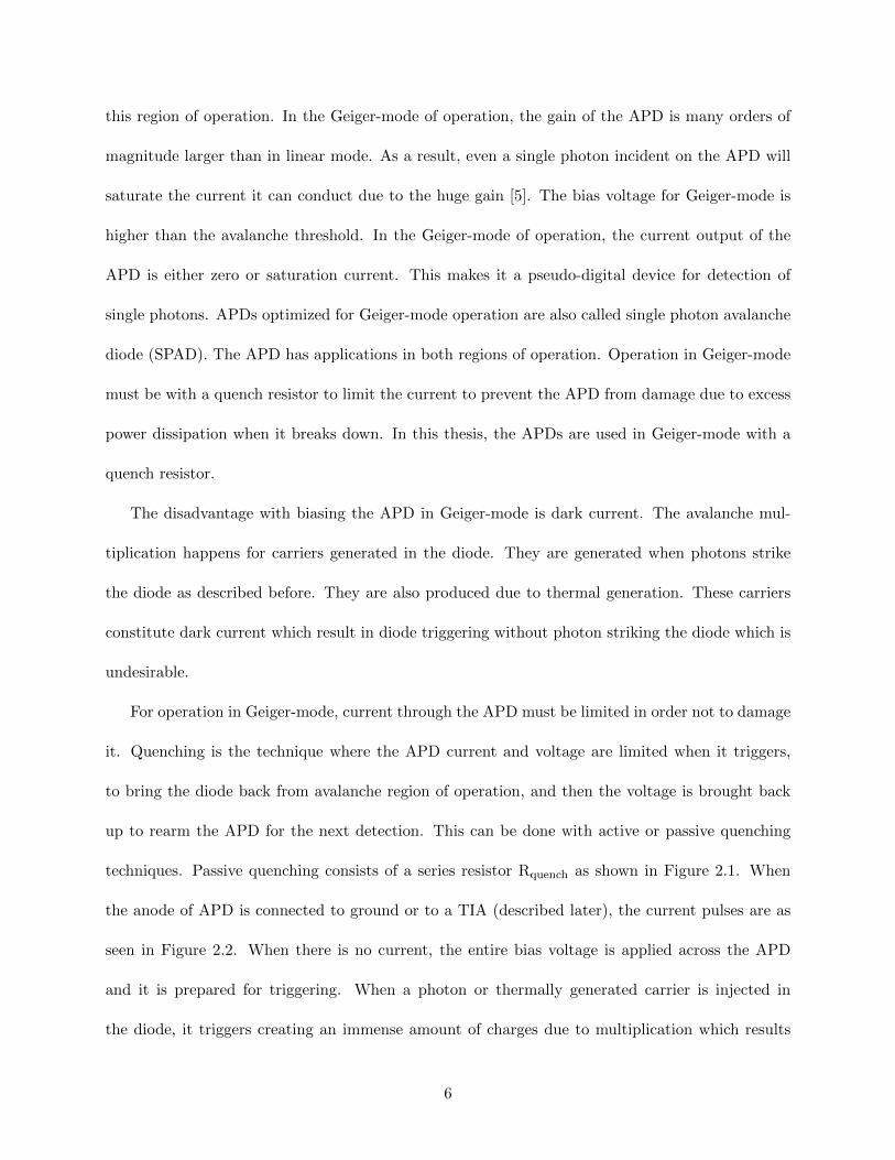
techniques. Passive quenching consists of a series resistor Rquench as shown in Figure 2.1. When
the anode of APD is connected to ground or to a TIA (described later), the current pulses are as
seen in Figure 2.2. When there is no current, the entire bias voltage is applied across the APD
and it is prepared for triggering. When a photon or thermally generated carrier is injected in
the diode, it triggers creating an immense amount of charges due to multiplication which results
6

in large current. This current through the quenching resistor drops a large voltage bringing the
voltage across the APD below the avalanche region. The voltage slowly builds back up as the APD
depletion capacitance charges through the quench resistor. This cycle repeats to create current
pulses that are the output of APD.
HV
Rquench
APD
CAPDIAPD
Figure 2.1: Schematic and simple electrical model of APD in Geiger-mode
time
Dead time
trigger trigger
AP
D c
urre
nt
Figure 2.2: Waveform of output current from APD when triggered in Geiger-mode operation
As seen in Figure 2.2, when the APD triggers, it takes a finite amount of time to recharge back
to avalanche voltage. This is a function of diode capacitance and quench resistance. This is called
the dead time in which the APD does not respond to incoming photons.
In Geiger-mode of operation with a series quench resistor, the quenching action happens due
7

to the APD’s negative differential resistance in the breakdown region [6] which creates a relaxation
action. Otherwise, the series combination of Rquench and APD capacitance would settle at a stable
stagnant state and would not go between two states of armed and discharged.
The physical layout and cross sectional view of the APD is seen in Figure 2.3 [7]. As the APD
is fabricated in the AMS SiGe 0.35 µm BiCMOS process, the diffusion is a graded SiGe.
Figure 2.3: Cross sectional view of layers of APD fabricated in AMS SiGe 0.35 µm BiCMOS process
Peak current from Geiger-mode breakdown of the APD can be calculated using Equation (2.2)
where IAPD,trigger is the peak APD breakdown current, Vbias is the applied reverse bias voltage,
Vbreakdown is the avalanche breakdown voltage of the APD and Rquench is the value of series quench
8

resistor.
IAPD,trigger =Vbias − Vbreakdown
Rquench(2.2)
In an APD, ambient light level appears as a constant count rate per unit time. When there is
an additional light pulse incident on the APD, the count rate (pulse rate) goes up for that brief
time when the incident pulse appears. By counting the pulses in a unit time and allocating them
into bins, the bin corresponding to the incoming pulse can be seen to have a higher value than the
other bins. Without any pulse, when the APD is in complete darkness, the bins contain the dark
count which are pulses due to dark current as explained earlier.
Figure 2.4 shows the operation of an APD fabricated in AMS SiGe 0.35 µm BiCMOS pro-
cess. This APD has a photoactive area of 24 µm×24 µm. The plot shows the voltage across the
quench resistor of 210 kΩ. The breakdown voltage of the APD is calculated using Equation (2.2).
The breakdown voltage values calculated using different bias voltages are seen in Table 2.1. The
breakdown voltage is constant at about 11.27 V irrespective of the applied bias voltage.
Vbias IAPD,trigger Vbreakdown
in volts in µA in volts
11.50 1.07 11.2811.75 2.29 11.2712.00 3.50 11.27
Table 2.1: Calculating the breakdown voltage of APD in AMS SiGe 0.35 µm BiCMOS process
Each photon striking the APD is not guaranteed to trigger it even though the APD is armed
and not in the dead time. The ratio of number of incident photons to number of trigger events is
called the photon detection efficiency of the APD at a particular wavelength. The plot of photon
detection efficiency versus wavelength would show the most sensitive region of operation of the
APD where most of the incoming photons results in trigger events.
As seen in Figure 2.1, a simple electrical model for the APD is a current source in parallel with
9

Figure 2.4: Measured output current from APD in Geiger-mode operation. Applied Vbias = 11.5 Vwith Rquench = 210 kΩ
its junction capacitance value. This model is used to simulate the APD with the TIA later.
The maximum incoming light pulse frequency that can be detected using the APD is the inverse
of its dead time. If the incoming pulse frequency is higher, this causes an aliasing effect where the
detected frequency starts decreasing. This is illustrated in Figure 2.5 as adapted from [1].
2.1.2 Silicon Photomultiplier
A Silicon Photo-Multiplier (SiPM) is solid state analog of the PMT. This is not a perfect analogy
since the SiPM output is quantized. An SiPM is an array of APDs operating in Geiger-mode
all connected in parallel. The output of the SiPM can be seen to be a combination of all APD
responses and current pulses added together. The currents from all APDs are added together by
just connecting the anodes of the all APDs in parallel. The SiPM is a pseudo-analog device where
10

Incident pulse rate (MHz)
SiPMAPD
Det
ecte
d ra
te (
MH
z)
Figure 2.5: Output pulse rate vs incident pulse rate of SiPM and APD. Adapted from [1]
the output pulse is quantized to the value of an APD current. The internal schematic of the SiPM is
as seen in Figure 2.6. This figure also shows the simple electrical model of the SiPM which is similar
to the APD but the current source ISiPM can have different values and the parallel capacitance
CSiPM is the sum of all APD capacitances in the SiPM array.
HV
Rquench
APDs
CSiPMISiPM
SiPM
Figure 2.6: Schematic and simple electrical model of SiPM
Figure 2.7 shows the physical layout of an SiPM with 64 (8×8) APDs implemented in AMS
SiGe 0.35 µm BiCMOS process. This is an array of APDs with the quench resistor wrapped around
each of them. The quench resistor is implemented as poly2 resistors with value of 236 kΩ. The
11
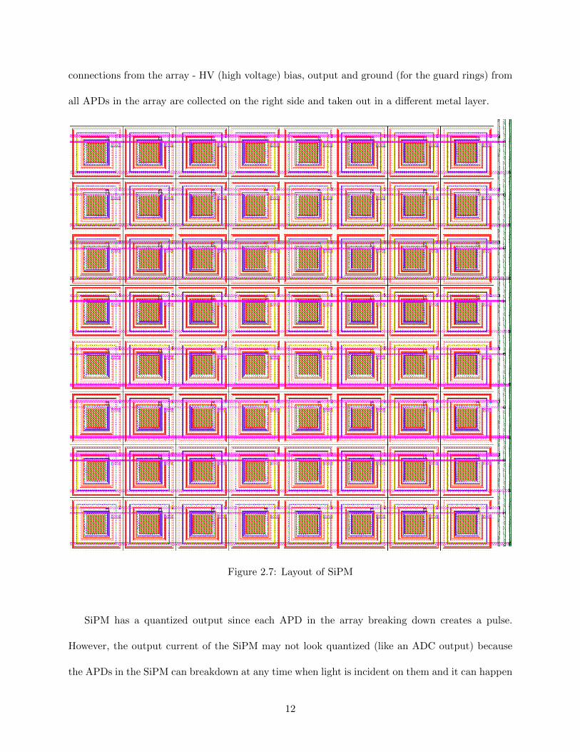
connections from the array - HV (high voltage) bias, output and ground (for the guard rings) from
all APDs in the array are collected on the right side and taken out in a different metal layer.
Figure 2.7: Layout of SiPM
SiPM has a quantized output since each APD in the array breaking down creates a pulse.
However, the output current of the SiPM may not look quantized (like an ADC output) because
the APDs in the SiPM can breakdown at any time when light is incident on them and it can happen
12
when one APD is quenching in the dead time with the decaying slope. The SiPM output current
is the additive combination of the characteristics of all its APDs.
The advantage of SiPM over APD is that it can detect multiple photons at the same time. The
maximum number of photons an SiPM can detect concurrently is equal to the number of APDs
the SiPM consists of, assuming 100% photon detection efficiency, which is not the case practically,
but it gives an intuitive understanding of device operation. This manifests as higher frequency
response as shown in Figure 2.5. In this figure (adapted from [1]), the x-axis shows the incident
pulse rate and the y-axis shows the detected pulse rate. When the incident pulse rate is higher than
the inverse of APD dead time, the resulting response from the APD starts decreasing. Whereas,
the SiPM can respond at higher pulse rates since the the incident photon can land on a different
APD which is armed instead of the same APD in the dead time.
Vbias IAPD,trigger Maximum SiPM currentin volts in µA in µA
11.50 0.97 62.3711.75 2.03 130.1712.00 3.09 197.97
Table 2.2: Maximum SiPM current using APDs with Rquench = 236 kΩ in AMS SiGe 0.35 µmBiCMOS process
The maximum current from the SiPM is the sum of all APD currents in the array if all the APDs
trigger at the same time. This can be given by Equation (2.3) where ISiPM,max is the maximum
SiPM current, N is the number of APDs in the SiPM and IAPD,trigger is the maximum APD trigger
current which is given by Equation (2.2).
ISiPM,max = N · IAPD,trigger (2.3)
Table 2.2 shows the maximum SiPM breakdown currents at different bias voltages. The maxi-
mum current from the SiPM increases with bias voltage. Since higher bias voltage results in higher
quench currents, the APD capacitance can get charged back faster thus reducing the dead time.
13

But the tradeoff is that TIA DC current range (explained in Section 3.4.2) needs to be higher.
Higher bias voltages also result in higher dark count rates.
In an SiPM, the ambient level appears as a constant current. This is the result of APDs breaking
down constantly corresponding to the ambient photon flux level. Light pulse higher than ambient
would break down a higher number of APDs for that brief period of time and would be seen as a
current spike on the output.
2.2 LiDAR
LiDAR stands for Light Detection and Ranging. It is a technique where light is used to measure
the distance to a target by sending a pulse of light and measuring the time taken for the pulse
to return after reflecting from the target. This is similar to RADAR which uses radio frequency
radiation for the same purpose. Both devices operate using a concept called time-of-flight (ToF)
where the time taken for a wave to travel a distance in a medium is measured. LiDAR has an
accuracy advantage over RADAR because it can resolve finer details in the target due to the lower
wavelength radiation used. However, LiDAR’s disadvantage over RADAR is that it is susceptible
to ambient light which can be minimized by the use of optical filters.
The choice of wavelength to use in the LiDAR must consider safety to human eyes and at-
mospheric absorption. Longer wavelength light in the infra-red region is not focused by human
eyes and does not cause damage at low intensities. Atmospheric gases have different absorption
wavelength bands and the choice of light wavelength for LiDAR must fall outside these so that it
does not experience much attenuation when traveling through the atmosphere.
The sensitivity of photodetector is one of the factors that determine a LiDAR’s maximum range.
The reflected light intensity decreases exponentially with distance. The photodetectors must be
able to detect individual photon level of light flux in order for the LiDAR to have good range which
14

is especially required when used in airborne geological applications.
LiDAR’s are useful in applications where a three dimensional map of the object needs to be
generated. Examples of such uses are listed below:
1. Geological terrain mapping – LiDAR’s are mounted to aircraft and scanned through a terrain
to generate a 3D map of the ground underneath. This is used in mapping forests.
2. Self-driving cars (ADAS systems) – LiDAR is mounted on automobiles to generate a 3D map
of the surroundings to process and navigate effectively through it.
As described earlier, the LiDAR sends a pulse of light and looks at the reflected return. The
pulse of light is usually generated using a LASER. This pulse duration is as short as possible to
increase range resolution. The shape of this pulse is close to gaussian. The width of this pulse
measured at the midpoint is called the full width half maximum (FWHM) width. This pulse hits
the target and returns back and strikes the photodetector. If the target has multiple features, there
would be reflections from each feature resulting in a complex reflected waveform.
Two types of implementing LiDAR front ends are described in the following sections. They are
the discrete return LiDAR and full waveform LiDAR. They have slightly different approaches to
detecting and time stamping the input pulse. The blocks needed for implementing discrete return
LiDAR are implemented in this thesis.
2.2.1 Discrete Return LiDAR
The block diagram of discrete return LiDAR (DR-LiDAR) is seen in Figure 2.8. This only shows
the receiving end of the LiDAR. It consists of the SiPM as photodetector interfacing with TIA
whose output is connected to the comparator. Output of comparator is used by an external TDC
(Time to Digital Converter) to time stamp the incoming pulse. Time stamping is the process of
recording the time at which the incoming pulse arrives with respect to the time at which pulse
15

was sent. The threshold voltage of comparator is set using an on-chip DAC. The TIA converts the
SiPM current to a corresponding voltage. The comparator output is higher if the TIA output is
higher than the threshold voltage and vice versa. The DAC generates a voltage corresponding to
an input digital code.
TIA
−
+
DAC
TDC
N-bit digital input
Comparator
Timing information
Off-chipSiPM
HV
Figure 2.8: Block diagram of discrete return LiDAR
The TIA, comparator and DAC are designed in this thesis and implemented on a chip. These
are described in chapters 3, 4 and 5.
The DR-LiDAR operation can be understood using Figure 2.9. This shows an example re-
flected/incoming waveform on the top and the corresponding output of the circuit on the bottom.
The trigger level is the DAC output voltage going into the comparator. The trigger level is set
close to the lowest level of the waveform which is the output of TIA for ambient light input. The
output of comparator is high when there are pulses present in the output above the trigger level.
This output goes into an external TDC (Time-to-Digital converter) which measures the time taken
by the pulse relative to the outgoing pulse time instant.
This example waveform contains multiple peaks corresponding to multiple features of the target.
For example in the case of airborne LiDAR used for remote sensing and geological mapping, when
the incident gaussian light pulse hits a tree from above, there would be multiple returns from the
16

time
Triggerlevel
return return return
Figure 2.9: Return waveform from the discrete return LiDAR
branches and sub-branches etc. When there are two pulses overlapping as seen in Figure 2.9, the
DR-LiDAR only detects the first pulse. This is the disadvantage of DR-LiDAR.
Equation (2.4) can be used to calculate the distance to target [8]. Here, τ is the time measured
from outgoing pulse to reflected pulse, c is the speed of light and n is the refractive index of the
medium which would be close to unity for atmosphere.
R =c
n· τ
2(2.4)
Range resolution is the minimum distance of features in the target which the LiDAR can resolve.
Range resolution can be calculated using equation (2.5) [8] where ∆τ is the minimum time between
pulses that the system can resolve, c is the speed of light and n is the refractive index of the medium
which would be close to unity for atmospheric propagation.
∆R =c
n· ∆τ
2(2.5)
17

From the equation for range resolution, we can infer that the outgoing light pulse needs to have
a width less than ∆τ for the range resolution to be dependent on the resolving time of the receiving
system so that the reflected pulses have clear peaks corresponding to the features of subject being
observed.
As seen in the example waveform described above, the DR-LiDAR can miss target features that
result in overlapping reflected pulses. But the advantage of DR-LiDAR is simplicity and the ease
of processing its output. The full waveform LiDAR described next with iterative deconvolution
algorithms can result in better extraction and better resolution even if the incoming waveforms
does not show pulses that are fully resolved.
2.2.2 Full Waveform LiDAR
The full waveform LiDAR (FW-LiDAR) samples the entire reflected waveform so that information
about features of target would not be lost. The block diagram of FW-LiDAR is seen in Figure 2.10.
It consists of the SiPM output going into a TIA which converts the SiPM current to voltage. Output
of TIA goes into an ADC (Analog-to-Digital converter) which samples the incoming waveform at
regular intervals and converts it to a digital number. The digital output is processed by DSP
(Digital Signal Processing) to extract the pulses and other features from the waveform. This is
seen in Figure 2.11.
DSP techniques such as gaussian decomposition is the conventional way to process and detect
the output from full waveform LiDAR. This technique essentially fits gaussian curves into the
LiDAR return waveform to identify multiple returns. Better techniques such as deconvolution
algorithms like Richardson-Lucy [8] [9] and Gold [10] are iterative algorithms that can better extract
reflections from targets that would otherwise not be identified with decomposition. A comparison
of the deconvolution algorithms can be seen in [11].
18

TIA Timing information
Off-chip
ADCDSPPost-ProcessingN-bit
SiPM
HV
Figure 2.10: Block diagram of full waveform LiDAR
returns returns returnstime
Figure 2.11: Full waveform LiDAR return signal waveform
Higher resolution recovery is possible using the full waveform LiDAR as the output from the
LiDAR can be post-processed using deconvolution algorithms to extract reflection signatures which
would go unnoticed with the discrete return LiDAR.
Discrete return LiDAR can be real-time because there is minimal post-processing. Full-waveform
LiDAR needs post-processing like the iterative deconvolution algorithms to be run on the waveform
data and then the pulses can be extracted. This is a tradeoff, because Full-waveform LiDAR can
resolve finer details but takes more time whereas discrete return LiDAR works quickly but is low
resolution. Therefore, these can be implemented based on the application.
19

Chapter 3
Transimpedance Amplifier (TIA)
As seen in Chapter 2, the output signal from photosensors like the avalanche photo diodes (APD)
and silicon photomultipliers (SiPM) is a current. As the circuits that process the output signal
of photosensors are voltage mode circuits like comparator or ADC, there is a need to convert
the output current from photosensors to voltage. This operation is done by the transimpedance
amplifier (TIA).
When designing a TIA to interface with an SiPM, the input current range of the TIA needs to
be high enough so that, even if all cells in the SiPM breakdown at the same time, the TIA would
be in the linear gain region and provide the appropriate output signal. This is not always possible
since the dynamic range of the TIA would have to be very high.
This chapter describes the design and analysis of transimpedance or transresistance amplifier
which is part of LiDARs and other applications as shown in Chapter 2.
A TIA circuit seen as a black box would take a current as an input and produce a proportional
voltage as the output. The transfer ratio between the output and input is the gain of the TIA and
has units of ohms. This is the underlying reason for the name.
In this chapter, firstly, using the resistor as a TIA will be described. Next, a CMOS TIA circuit
20

is introduced which is an improvement over the resistor TIA.
3.1 Resistor as TIA
A resistor by definition drops a voltage across its terminals that is directly proportional to the
current flowing through it. The ratio of voltage to current is its resistance value. This can be seen
as a passive TIA because the input current can be passed through the resistor, and the voltage
developed across the resistor can be taken as the output voltage. The transimpedance gain is
defined as the ratio of voltage output to current input. In this circuit, this would be the value of
the resistor RTIA. An example of this implementation is seen in Figure 3.1. In this circuit, an
APD is connected to a high voltage bias through a quench resistor. The other end of the APD is
connected to the TIA resistor. The voltage dropped across the TIA resistor is the output voltage.
HV
VOUT
Rquench
RTIA
APD
Figure 3.1: Resistor as TIA
This passive TIA has advantages and disadvantages as listed below [12]:
Advantages:
1. Simplicity – Does not take up much area and does not need a source of power.
2. Stability – Is inherently stable since feedback is not used.
Disadvantages:
21

1. Slow response and low bandwidth – The photosensor capacitance along with the TIA resistor
has a time constant that limits the bandwidth of this circuit. If TIA resistance is decreased
to increase the bandwidth, the gain goes down. Therefore, there is a tradeoff between the
two parameters.
2. Low signal-to-noise ratio (SNR) – The resistor adds noise in the circuit with RMS noise being
proportional to the resistor value [13, p. 225].
3. Change in photosensor bias voltage – The bias voltage across the photosensor must be kept
constant to get repeatable gain behavior. If the bias voltage across the photosensor changes,
its characteristics such as gain also changes. Using a resistor TIA, the bias voltage across the
photosensor depends on the amount of current it generates. This is undesirable.
Even with these disadvantages, this type of passive TIA is sometimes useful when low tran-
simpedance gain is sufficient.
3.2 Feedback TIA
The active TIA is an improvement over the passive resistor TIA in most aspects and gives better
performance in terms of bandwidth, drive capability and low input impedance. Active TIAs can
be broadly classified as below [14] :
1. Feedback TIA – In this type of TIA, the input current is applied to a gate or base of the
transistor and feedback resistor is between the input and output of the amplifier. The gain
of this TIA is usually the value of the feedback resistor. Inductors can be used to implement
peaking and extend the bandwidth of the amplifier [15].
2. Common-gate and common-base TIA, Regulated common-gate (RGC) TIA – The input cur-
rent is applied to source or emitter of the transistor in this type of TIA. These TIAs tend to
22

have lower input impedances, especially the RGC TIA [16]. Lower input impedance results
in higher bandwidth even with a photosensor that has high capacitance.
Figure 3.2 shows the basic block diagram of a feedback TIA. It consists of an inverting volt-
age amplifier with gain of −A whose input impedance is considered ideally infinite and output
impedance is considered ideally zero. The feedback resistor is connected between the input and
output terminals of this amplifier. The negative feedback type is shunt-shunt because the output
sampled quantity is voltage, and the input current is mixed into amplifier input current and feed-
back current [13, p. 1120]. Input current is iin. Voltage at the input is vin and output voltage is
vout.
-A
RF
iinvin
vout
Figure 3.2: Basic block diagram of feedback TIA
Figures 3.3 and 3.4 show practical implementations of the feedback TIA. In these figures, the
inverting voltage amplifier is implemented using an opamp in inverting configuration and a CMOS
inverter respectively.
The transimpedance gain of the basic feedback TIA seen in Figure 3.2 is analyzed as follows:
For the voltage amplifier, we know that,
vout = −A · vin (3.1)
The input current only passes through the feedback resistor since the input impedance of the voltage
amplifier is infinite. This results in,
vin − vout = iin ·RF (3.2)
23

−
+
RF
VBIAS
iin vin
vout
Figure 3.3: Feedback TIA using opamp
RF
VDD
iin vin vout
Figure 3.4: Feedback TIA using CMOS inverter
Substituting Equation (3.1) in (3.2),
vout = − iin ·RF
1 + 1A
(3.3)
The transimpedance gain is given as,
ZT =voutiin
= − RF
1 + 1A
(3.4)
To find the voltage on input node due to input current, substituting Equation (3.1) in (3.2),
vin =iin ·RF
1 +A(3.5)
This can be written in terms of the input resistance which is the ratio of input voltage change to
input current,
Rin =viniin
=RF
1 +A(3.6)
The above equation shows that when a current is applied to the feedback TIA input, the voltage
on input only changes by this factor which is much lower than the voltage change when using a
resistor as TIA. This ensures minimal change of bias voltage across the photosensor which does not
change its gain.
24

For large values of A, The TIA gain, Equation (3.4) reduces to,
ZT =voutiin
= −RF (3.7)
The above result shows that ideal transimpedance gain of the feedback TIA is equal to the feedback
resistance value.
The input resistance of the TIA tends to zero for large values of A as seen from Equation (3.6).
This is an important result as seen in later analysis of the TIA.
3.3 CMOS TIA
In this section, an active feedback TIA is designed in a CMOS process. The implementation is
using AMS SiGe 0.35 µm BiCMOS process. Figures 3.5 and 3.6 show the complete schematic of
the CMOS TIA designed for this thesis.
This circuit is designed in AMS SiGe 0.35 µm BiCMOS process. IIN is the current from the
photodetector and VOUT is the voltage output. The circuit is configured in shunt-shunt feedback
TIA topology [13, p. 1105]. The feedback resistance is placed between the input and output of the
first stage. The feedback resistance consists of different values of digitally switchable resistors that
vary the gain. A variable gain is implemented to change the dynamic range of the TIA. This would
be useful when an SiPM is connected to the TIA and the gain can be set based on the maximum
current to be detected which is proportional to the number of cells firing at the same time in the
SiPM.
The first stage is a PMOS based inverting differential amplifier that is configured as a TIA,
and the second stage is a source follower which is a noninverting buffer to drive the load. The first
stage is similar to Figure 3.3 where VBIAS is generated using the resistors R1 and R2 forming a
voltage divider to bias the non-inverting terminal. MP1, MP2 and MP3 form a current mirror used
to bias the first and second stages. R3 is used to set the current in the gate-drain connected MP1
25
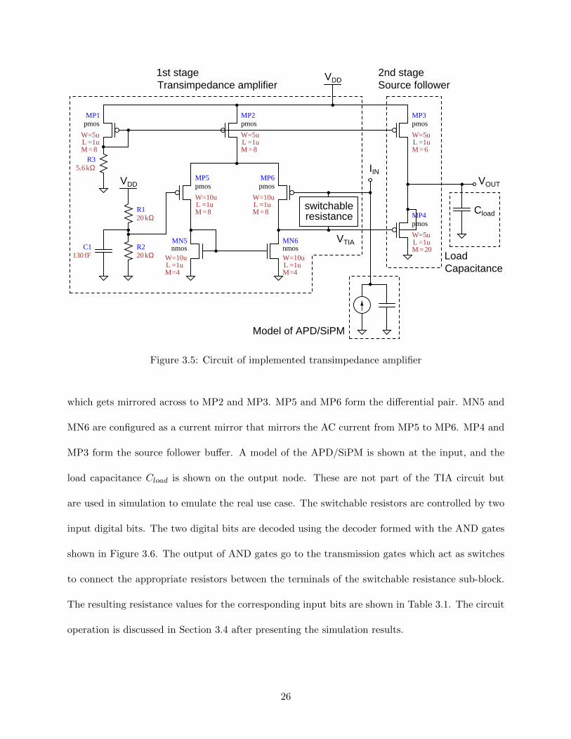
W=5uL =1uM=8
MP1pmos
W=10uL =1uM=4
MN6nmos
W=10uL =1uM=8
MP5pmos
W=5uL =1uM=8
MP2pmos
W=10uL =1uM=8
MP6pmos
W=10uL =1uM=4
MN5nmos
5.6 kΩR3
130 fFC1
20 kΩR1
VDD
20 kΩR2
W=5uL =1uM=6
MP3pmos
W=5uL =1uM=20
MP4pmos
VDD
Cload
VOUT
IIN
Model of APD/SiPM
LoadCapacitance
1st stageTransimpedance amplifier
2nd stageSource follower
switchableresistance
VTIA
Figure 3.5: Circuit of implemented transimpedance amplifier
which gets mirrored across to MP2 and MP3. MP5 and MP6 form the differential pair. MN5 and
MN6 are configured as a current mirror that mirrors the AC current from MP5 to MP6. MP4 and
MP3 form the source follower buffer. A model of the APD/SiPM is shown at the input, and the
load capacitance Cload is shown on the output node. These are not part of the TIA circuit but
are used in simulation to emulate the real use case. The switchable resistors are controlled by two
input digital bits. The two digital bits are decoded using the decoder formed with the AND gates
shown in Figure 3.6. The output of AND gates go to the transmission gates which act as switches
to connect the appropriate resistors between the terminals of the switchable resistance sub-block.
The resulting resistance values for the corresponding input bits are shown in Table 3.1. The circuit
operation is discussed in Section 3.4 after presenting the simulation results.
26

switchableresistance
D0
D0 D1 D2 D3
D1 D2 D3
W=2uL =0.5uM=10
MN7nmos
W=8uL =0.5uM=10
MP7pmos
W=2uL =0.5uM=10
MN8nmos
W=8uL =0.5uM=10
MP8pmos
W=2uL =0.5uM=10
MN9nmos
W=8uL =0.5uM=10
MP9pmos
W=2uL =0.5uM=10
MN10nmos
W=8uL =0.5uM=10
MP10pmos
B1
B0
B0
B1
B1
B0
B0
B1D0
D0
D1
D1
D2
D2
D3
D3
IIN
VTIA
IIN
VTIA
2kΩ
R1
2kΩ
R2
4kΩ
R3
8 kΩ
R4
2 kΩ 2 kΩ 4 kΩ 8 kΩ
Figure 3.6: Circuit of switchable resistance
3.3.1 Simulation results
Simulation results of the TIA in Figure 3.5 are shown in sections below:
DC analysis
In this simulation, the input DC current is swept and the output voltage is plotted. Figure 3.7
shows the output voltage for different gain settings. Figure 3.8 shows the slope (gain) of these
curves which shows the linear gain region (inverted plateau) and the actual gain value. In both
these curves, the x-axis is the applied DC current. It is desirable to have a large positive range and
27

B1 B0 Feedback resistance
0 0 2 kΩ0 1 4 kΩ1 0 8 kΩ1 1 16 kΩ
Table 3.1: Resistance values corresponding to input values of digital bits
a small negative range. The positive and negative input current ranges are shown in Table 3.4.
Figure 3.7: Output voltages for different gain settings with swept input current
Figure 3.8: Slope (gain) of output voltages in Figure 3.7
Transient analysis
In this simulation, a time changing input current is applied and the output voltage is plotted. The
input is a square wave current. Value of settling time can be extracted from these simulations
28

which is an important parameter. The settling time is the amount of time the TIA output takes to
settle to the right value once the input stops changing. Here, settling time to 2% of the final value
is measured as shown in Figure 3.10. Figure 3.9 shows output voltage for different gain settings.
The rise time is inversely proportional to the bandwidth of the amplifier. Tables 3.10, 3.11, 3.12
and 3.13 on Page 46 show the settling time for different values of capacitance on input. Table 3.2
shows the power consumption of the circuit for an input square wave of 1 MHz.
Figure 3.9: Transient output voltage for different gain settings
Figure 3.10: Measuring settling time
29

B1 B0 Feedback resistance RMS power in mW
0 0 2 kΩ 7.080 1 4 kΩ 7.081 0 8 kΩ 7.091 1 16 kΩ 7.10
Table 3.2: Power dissipation of TIA at different gain settings
AC small-signal analysis
AC small-signal analysis shows the frequency response of the circuit. In this simulation, the entire
circuit is linearized at a particular bias value and the output response is calculated for the given
input. As a result, the non-linearities due to large signal response are not seen or considered.
Figure 3.11 shows the output voltage for different values of capacitance on input. This result is
with zero input DC bias current. The bandwidth of TIA for different gain values are shown in
Tables 3.10, 3.11, 3.12 and 3.13 on Page 46.
Figure 3.11: Small-signal AC simulation showing output voltage
3.3.2 Physical layout
Integrated circuit layout of the TIA is shown in Figure 3.12. In an analog circuit, the differential
pair devices need to match so that the devices have the same characteristics on both sides and
the differential nature of the circuit is preserved. Current mirror devices need to be matched so
30
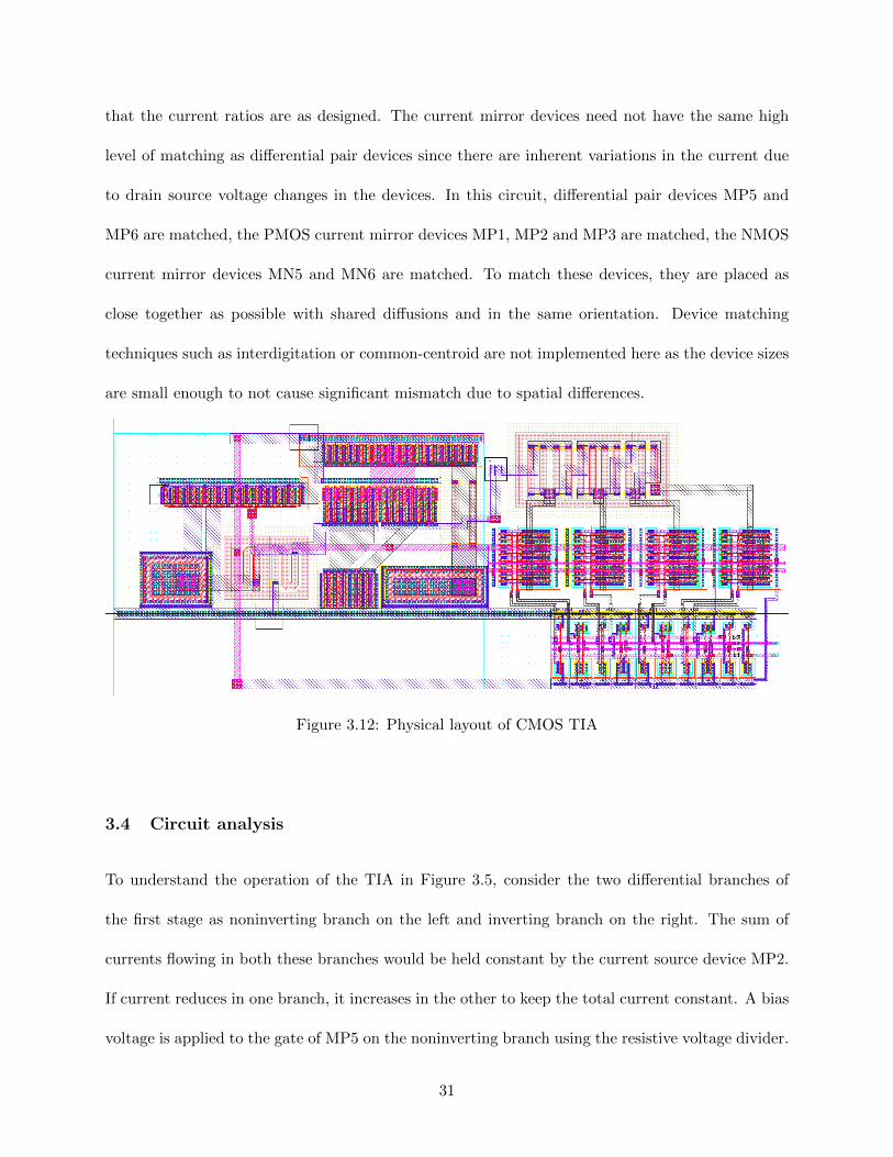
that the current ratios are as designed. The current mirror devices need not have the same high
level of matching as differential pair devices since there are inherent variations in the current due
to drain source voltage changes in the devices. In this circuit, differential pair devices MP5 and
MP6 are matched, the PMOS current mirror devices MP1, MP2 and MP3 are matched, the NMOS
current mirror devices MN5 and MN6 are matched. To match these devices, they are placed as
close together as possible with shared diffusions and in the same orientation. Device matching
techniques such as interdigitation or common-centroid are not implemented here as the device sizes
are small enough to not cause significant mismatch due to spatial differences.
Figure 3.12: Physical layout of CMOS TIA
3.4 Circuit analysis
To understand the operation of the TIA in Figure 3.5, consider the two differential branches of
the first stage as noninverting branch on the left and inverting branch on the right. The sum of
currents flowing in both these branches would be held constant by the current source device MP2.
If current reduces in one branch, it increases in the other to keep the total current constant. A bias
voltage is applied to the gate of MP5 on the noninverting branch using the resistive voltage divider.
31

Consider the case when the input current, IIN is zero. The current flowing through the feedback
resistance is zero since the gate of MP6 does not take current. There is no voltage drop across the
feedback resistor and the two nodes are essentially shorted. If the voltage on gate of MP6 increases,
it shuts off more and reduces the current in that branch. This increases the current in MP5 which
is mirrored across to MN6. The device MP6 shutting off and the device MN6 turning on results in
the output node going down. Since this node is connected through the feedback resistance to the
gate of MN6, it prevents the initial increase in voltage. This is the feedback action and this ensures
the gate of MP6 is ideally same as the gate of MP5 which is the bias voltage. Now consider the
case when there is a current IIN flowing into the input. This current needs to flow into the feedback
resistor as there is no other path. If this current is not taken by MN6, it tries to increase the
gate voltage of MP6. As explained before, due to the feedback action, the gate of MP6 is ideally
same as the bias voltage. As a result, the output voltage changes to accommodate for the extra
current put into that node. The output voltage change would be equal to the voltage drop across
the feedback resistor due to the input current. This results in a transimpedance gain same as the
value of feedback resistance.
By switching in different values of resistor using transmission gate switches, we can achieve
different gain values for the TIA. This is the idea behind the switchable resistance implementation
shown in Figure 3.6. The resistance value is increased by putting resistors in series by turning on
particular switches. The switches are made using transmission gates which are PMOS and NMOS
devices in parallel. Out of the four transmission gates, only one would be on at a time so that
the right number of resistors are put in series. The transmission gates are turned on according
to an input 2-bit digital code. This input digital code is decoded from 2-bit binary to 4 outputs
corresponding to the binary code using a 2:4 decoder shown in the same schematic. The outputs
of decoder drive the transmission gates.
32

As explained before, when a current is input to the TIA, the input voltage ideally does not
change due to the feedback action. This is seen as a zero input resistance since there is no change
in voltage for an input current. Practically this is not the case and the input has a finite resistance
as explained in Section 3.4.4.
To stabilize feedback TIAs, compensation capacitors might be connected in parallel with the
feedback resistance. This is not needed in this TIA since the delay of the amplifier is low enough
that feedback does not cause significant stability issues. Instability would be seen as transient
ringing in the output voltage. Ringing is present to a small degree but decays quickly and settles
to the intended value.
Since the first and second stages are DC coupled, the voltage ranges between both must be
compatible. The linear output range of the first stage must be same or larger than the linear input
range of second stage. The output range of the first stage spans from the bias voltage of MP5 to
the VDS of MN6. This range is compatible with the PMOS source follower.
Design considerations for choosing parameters in the circuit – Bias voltage on the gate of MP5 is
set as high as possible and still accommodate for VSG,MP5 and VSD,MP2 to maximize output voltage
range and in turn maximize input DC range. The bias current through the differential branches
are set high enough so that the input current range is maximized without consuming too much
power. The devices are sized to take this current without having a high VGS . The differential input
devices are large to have high gm to increase open loop gain. This has another benefit that if the
gm of differential device is high, the input impedance will be low and result in higher bandwidth.
However, this might also negatively affect the bandwidth because of increased capacitance on the
first stage output node. The NMOS current mirror devices are large enough that their VDS does
not limit the output range. In the source follower, the amplifying device is large because it sinks
33

current from the current source as well as the load. Also, its body terminal is connected to its
source to prevent its body effect from reducing the gain. Following sections discuss and analyze
each aspect of the TIA design.
3.4.1 Switchable resistance
The switchable resistance is used to implement different gain settings in the TIA. The circuit for
switchable resistance is seen in Figure 3.6. In this circuit, the transmission gates (TG) switch the
resistors R1, R2, R3 and R4 in different series combinations to achieve the desired value as the
feedback resistance according to Table 3.1. R1, R2, R3 and R4 are implemented as high resistance
poly2 resistors. For achieving a resistance of 2 kΩ, only the TG consisting of MP7 and MN7 is
turned on with the others off. For a resistance of 4 kΩ, the TG consisting of MP8 and MN8 is
turned on. For a resistance of 8 kΩ, the TG consisting of MP9 and MN9 is turned on. For a
resistance of 16 kΩ, the TG consisting of MP10 and MN10 is turned on. The TG switches are
controlled using the decoder shown on the bottom part of the figure. The decoder generates four
sets of true and complementary outputs that control the PMOS and NMOS in the transmission
gates. The decoder outputs are such that only one TG would be on for each digital input code.
The total resistance offered by the switchable resistance block is the sum of feedback resistor
and TG resistance. For each digital input code, only a single TG resistance adds up to the total
resistance. The TG resistance must be much lower than the feedback resistance to not affect the
TIA gain significantly.
The transmission gate resistance is the parallel combination of the PMOS resistance and the
NMOS resistance [13, p. 830]. To turn on the transmission gate, the PMOS gate is tied to ground
and the NMOS gate is tied to VDD. Figure 3.13 shows a transmission gate. This circuit can be
analyzed by assuming V1 > V2. The gate to source voltages for PMOS and NMOS can be given by
34

the following equations,
VDD VDD
V1
V2
VSG
VGS
V1 > V2
+
-+
-
Figure 3.13: Transmission gate circuit
For the PMOS,
VSG = V1 (3.8)
VSD = V1 − V2 (3.9)
For the NMOS,
VGS = VDD − V2 (3.10)
VDS = V1 − V2 (3.11)
The resistance of PMOS is highest when VSG is close to VTHP , the threshold voltage of the
PMOS. Similarly, the resistance of NMOS is highest when VGS is close to VTHN , the threshold
voltage of the NMOS.
Figure 3.14 shows the resistance of the transmission gate when V2 is ground and V1 is swept
from 0 to VDD. The other curves in this plot show the resistance of PMOS and NMOS standalone.
It is visually apparent that the TG resistance is the parallel combination of the PMOS and NMOS
resistance. The TG resistance ranges from about 100 Ω to 800 Ω.
In this application, V1 is connected through the feedback resistor in series to IIN and V2 is
connected to VTIA.
35

Figure 3.14: Resistance of transmission gate used to switch feedback resistors
The resistance of the TG in Table 3.3 is measured by applying the voltages on IIN and VTIA
across the TG for every input range. This emulates the operating conditions of the TG in the TIA.
From this table, we can see that the percentage error of TG resistance to feedback resistor is less
than 10% for the entire input current range in every gain setting. Therefore, the TG resistance
does not affect the TIA gain significantly. The TG resistance increases proportional to the feedback
resistance so that the total resistance does not have significant contribution from the TG resistance.
TIA input TIA first stage TG resistance TG resistanceB1 B0 RF range output range range as percentage
in µA in volts in Ω of RF
0 0 2 kΩ 0 to 176 2.48 to 2.32 164.1 to 149.1 8.2% to 7.5%0 1 4 kΩ 0 to 271 2.48 to 1.71 218.3 to 158.0 5.5% to 4.0%1 0 8 kΩ 0 to 294 2.48 to 0.49 436.7 to 128.1 5.5% to 1.6%1 1 16 kΩ 0 to 147 2.48 to 0.32 504.6 to 126.0 3.2% to 0.8%
Table 3.3: Transmission gate resistance
3.4.2 TIA input DC range
For a TIA to provide the right output voltage for the given input current, the TIA needs to have
uniform gain for the entire input current range. This is especially important when interfacing the
TIA with an SiPM as it can generate a large current if all the APDs in its array break down. A
36

photodetector mainly outputs current in one direction, positive in this case. So, the TIA needs to
have a large positive input DC current range. Furthermore, it is better to design the TIA with a
slight negative range so as to accommodate for circuit parameter changes due to process, voltage
and temperature variations.
The input DC current range of a TIA is affected by a number of factors. As the TIA input
current is taken by the inverting branch of the differential amplifier, specifically MN6. This input
current replaces the bias current already flowing in that branch. As a result, the input DC range
is proportional to the bias current flowing in that branch. However, increasing the bias current
to increase DC range would also increase the power consumption of the circuit. Increasing the
differential device sizes also increases the DC input range especially the positive input range.
Table 3.4 shows the input DC current range for different values of feedback resistances. The
range is measured until the gain drops to within 10% of the peak gain value. A lower gain setting
gives more range span. This is a tradeoff of gain and range. These values are designed to be higher
than the maximum SiPM output as seen in Table 2.2.
B1 B0 Feedback resistance Input DC range Output voltage range
0 0 2 kΩ -168 µA to 176 µA 4.24 V to 3.94 V0 1 4 kΩ -74 µA to 271 µA 4.29 V to 3.34 V1 0 8 kΩ -27 µA to 294 µA 4.26 V to 2.15 V1 1 16 kΩ -12 µA to 147 µA 4.26 V to 1.98 V
Table 3.4: Input DC current range for linear gain to within 10% of maximum gain
3.4.3 TIA gain
As mentioned before, the gain of feedback TIA must be ideally same as the feedback resistance
value. But due to finite open loop gain value and the source follower, the gain is reduced. Table 3.5
shows the gain values of the TIA for different gain settings. The gain values are negative as the
differential amplifier first stage is inverting and the second stage is noninverting.
37

B1 B0 Feedback resistance TIA gain
0 0 2 kΩ -0.9 kΩ0 1 4 kΩ -2.84 kΩ1 0 8 kΩ -6.74 kΩ1 1 16 kΩ -14.44 kΩ
Table 3.5: TIA gain for different gain settings
As the TIA uses negative feedback, to analyze its gain, the feedback loop needs to be broken
[13, p. 1111]. The schematic used for TIA gain simulation is shown in Figure 3.15. For simulation,
the feedback loop is broken for AC currents and not DC as the feedback is necessary at DC to
bias the circuit properly in the gain region. The big inductor and capacitor (values in the order of
1000’s) in the schematic are added for this purpose. A resistor having the same value as feedback
resistance is added as load on the output terminal. This emulates the loading of feedback resistance
on the output terminal since the output node needs to sink or source the input current when the
feedback loop is closed. Only the first stage of the amplifier has feedback and is shown here. The
total gain would be the product of first stage gain and second stage gain.
To derive and analyze the small-signal AC gain of the TIA, the circuit shown in Figure 3.16 is
used. In this schematic, only AC voltages and currents are considered and the circuit is assumed to
be DC biased properly in the intended region. This is similar to the schematic used for simulation
shown in Figure 3.15. The capacitance has been replaced by a short and the inductance with an
open which reflects their behavior to AC currents. The biasing device MP2 is removed as DC
current sources look like an open in small signal AC sense. The gate of MP5 is grounded as the
bias voltage looks like a short for small signal AC currents. The open loop gain expression for the
circuit in Figure 3.16 is derived below.
Applying Kirchoff’s voltage law,
vsg5 − vsg6 = iin ·RF (3.12)
38

W=5uL =1uM=8
MP1pmos
W=10uL =1uM=4
MN6nmos
W=10uL =1uM=8
MP5pmos
W=5uL =1uM=8
MP2pmos
W=10uL =1uM=8
MP6pmos
W=10uL =1uM=4
MN5nmos
5.6kΩR3
130fFC1
20kΩR1
VDD
20kΩR2
VDD
IIN
VTIA
bigbig
RF
big
RF
Figure 3.15: Schematic for open loop gain simulation of TIA first stage
Knowing the following relationships for small signal operation of MOSFETs, where gmp5 and gmp6
are the transconductance of the devices,
vsg5 =i5gmp5
and vsg6 =i6gmp6
(3.13)
Substituting these values in Equation (3.12),
i5gmp5
− i6gmp6
= iin ·RF (3.14)
Because of the NMOS current mirror, the AC currents on the left branch is mirrored to the right
branch,
i5 = −i6 (3.15)
Substituting this relationship into equation (3.14)
− i6gmp5
− i6gmp6
= iin ·RF (3.16)
39

W=10uL =1uM=4
MN6nmos
W=10uL =1uM=8
MP5pmos
W=10uL =1uM=8
MP6pmos
W=10uL =1uM=4
MN5nmos
IIN
i5 i6
iinvin
vtia
+
-vsg6
+-
vsg5
RF
RF
Figure 3.16: Schematic for small signal open loop gain analysis
i6 =−iin ·RF1
gmp5+ 1
gmp6
(3.17)
Now to calculate the small signal output voltage vout. It is the voltage developed across the
resistance seen at that node due to resultant current. The resultant current on the right branch is
the difference of PMOS current and NMOS current which is (i6 − i5). The resistance seen at the
vout node is (rop6 ‖ ron6 ‖ RF ). Here, vout is used to represent vtia. This can be written as,
vout = (i6 − i5) · (rop6 ‖ ron6 ‖ RF ) (3.18)
Using equation (3.15),
vout = 2 · i6 · (rop6 ‖ ron6 ‖ RF ) (3.19)
Solving for i6,
i6 =vout
2 · (rop6 ‖ ron6 ‖ RF )(3.20)
Substituting equation (3.20) in equation (3.17),
vout2 · (rop6 ‖ ron6 ‖ RL)
=−iin ·RF1
gmp5+ 1
gmp6
(3.21)
40

Rearranging this equation, we get the small-signal open loop gain, AOL for the TIA first stage
AOL =voutiin
=−2 ·RF1
gmp5+ 1
gmp6
· (rop6 ‖ ron6 ‖ RF ) ≈−2 ·R2
F1
gmp5+ 1
gmp6
(3.22)
If gmp5 = gmp6 = gmp, this becomes,
AOL =voutiin
= −gmp ·RF · (rop6 ‖ ron6 ‖ RF ) ≈ −gmp ·R2F (3.23)
The following are small-signal operating point parameters for the MOSFETs which are extracted
from an operating point simulation of the circuit,
gmp5 = 850 µA/V , gmp6 = 835.5 µA/V
rop5 = 98.1 kΩ , ron6 = 403.2 kΩ
Substituting these parameters in equation (3.22) we get the values listed in Table 3.6 which also
shows the simulated values. We can see that they match closely.
B1 B0 RF Calculated AOL Simulated AOL
0 0 2kΩ -3.29kΩ -3.81kΩ0 1 4kΩ -12.83kΩ -13.85kΩ1 0 8kΩ -48.97kΩ -50.94kΩ1 1 16kΩ -179.36kΩ -183.02kΩ
Table 3.6: Calculated and simulated open loop gain of TIA first stage
The closed loop gain, ACL, is given by Equation(3.24) derived using feedback theory [13,
p. 1100]. Here, β is the feedback factor given by Equation (3.25). The value of AOL substituted
here must be a positive number since the equation assumes negative feedback. The negative sign
of the gain value implies that the amplifier is inverting. By having the feedback resistor between
the input and output terminals of the inverting amplifier, negative feedback is achieved.
ACL =AOL
1 + βAOL(3.24)
β =1
RF(3.25)
41

Substituting the values for β and AOL in Equation (3.24), we get the values listed in Table 3.7
which also shows the simulated values. The calculated values deviate from the simulated values
due to nonidealities such as variation of transconductance values for the two PMOS devices in the
differential pair and finite output resistance of these devices.
B1 B0 RF Calculated ACL Simulated ACL
0 0 2 kΩ -1.24 kΩ -0.95 kΩ0 1 4 kΩ -3.05 kΩ -2.93 kΩ1 0 8 kΩ -6.88 kΩ -6.89 kΩ1 1 16 kΩ -14.69 kΩ -14.81 kΩ
Table 3.7: Calculated and simulated closed loop gain of TIA first stage
The closed loop gain of the entire TIA is product of gains of first stage and second stage. The
second stage gain is very close to unity as it is a buffer amplifier and described in Section 3.4.5.
3.4.4 TIA input impedance and bandwidth
Input impedance
In the TIA circuit, input impedance is the ratio of voltage change on the input node to the current
applied to input.
It is desirable for the input impedance of a TIA to be ideally zero at all frequencies. This is
so that when a source of current is connected to the TIA, all of it flows into the TIA and gets
converted to corresponding output voltage. Even if the source of current has a parallel impedance,
it would not affect the performance. This is because the input current would have two paths to
flow, one through its internal impedance and the other into the TIA input. Current takes the path
of least resistance. Therefore, if the input impedance of the TIA is much lower than the parallel
impedance of the input current source, most of the current flows into the TIA.
For the photosensors discussed in Chapter 2, the parallel impedance is due to their junction
42

capacitance. For the APD, this is seen in the equivalent electrical model in Figure 2.1. At a certain
frequency, if the impedance of the parallel capacitance (CAPD) is lower than or comparable to the
TIA input impedance, the TIA gain decreases since the TIA does not get all the current generated
from the APD. This is the reason for frequency roll off.
To calculate the input impedance of the TIA, we can use the feedback Equation (3.26) [13,
p. 1105] where Rinf is the closed-loop input impedance, Ri is the open-loop input impedance, β is
the feedback factor and AOL is the open-loop gain.
Rinf =Ri
1 + βAOL(3.26)
From the previous section, substituting the values of AOL and β from Equations (3.23) and
(3.25),
Rinf =RF
1 + 1RF· gmp ·RF
2 =RF
1 + gmp ·RF(3.27)
For large values of RF , this reduces to,
Rinf ≈1
gmp(3.28)
The closed-loop input impedance for different gain settings are shown in Table 3.8.
B1 B0 RF Rinf
0 0 2 kΩ 0.75 kΩ0 1 4 kΩ 0.92 kΩ1 0 8 kΩ 1.04 kΩ1 1 16 kΩ 1.11 kΩ
Table 3.8: Closed-loop input impedance, Rinf of TIA
An intuitive explanation for the closed-loop input impedance is as follows. In the TIA circuit,
when a current ∆Iin is applied to the input, it cannot flow into the gate of MP6 and will flow
through the feedback resistance and into the NMOS device MN6. So, if we consider the initial
drain current through MP6 to be IMP6 when the input current was zero, when input current is
43

∆Iin, the current through PMOS would be (IMP6 −∆Iin). This change in current would be due
to a change in its gate voltage ∆Vsg6 which happens because of feedback action. Looking from the
input, applying a current ∆Iin would change the voltage there by ∆Vsg6. The ratio of these two
is the input impedance given by equation (3.29). This value of input impedance is approximate as
there are nonlinearities that change the input impedance at high frequencies.
Rinf ≈∆Vsg6∆Iin
=1
gmp6=
1
835.3 µA/V≈ 1.2 kΩ (3.29)
Bandwidth
The bandwidth of an analog circuit is determined by the poles in the circuit. Poles are created
by implicit and unintended RC circuits created in the circuit where a capacitance is driven by a
resistive source. For example an amplifier driving a capacitive load causes the frequency response
of the amplifier to be limited by the low pass RC circuit formed from the output resistance of the
amplifier and the capacitive load. When there are multiple poles in the circuit, the pole at the
lowest frequency would dominate the frequency response of the circuit. In the TIA circuit, there
are mainly two poles. One at the input node and another at the output node. At the input node,
the pole is created by the capacitance of photosensor and the input impedance of the TIA. At the
output node, the pole is created by the source follower driving a capacitive load. The first pole is
calculated next based on the input impedance calculated previously. The output pole is calculated
in the next section when source follower is discussed.
The junction capacitance of the photosensor like SiPM can be quite large in the tens to hundreds
of picoFarads. The capacitance is directly proportional to the number of APDs used in the array.
It also depends on the APD size. Higher the APD junction area, larger is the capacitance. The
values for capacitances used in Table 3.9 are chosen to cover estimated capacitance values for the
APD and SiPM.
44

To calculate the bandwidth due to input pole, we can use equation (3.30) where Rin is the input
impedance and Cin is the capacitance on input.
f3dB =1
2 · π ·Rin · Cin(3.30)
Table 3.9 shows the ideal bandwidth of the TIA for different values of input capacitance using Rin
values calculated for each gain setting in the previous section.
Capacitance Calculated f3dB Calculated f3dB Calculated f3dB Calculated f3dBon input for RF = 2kΩ for RF = 4kΩ for RF = 8kΩ for RF = 16kΩ
in pF in MHz in MHz in MHz in MHz
0.1 2125.5 1727.6 1528.7 1429.20.5 425.1 345.5 305.7 285.81 212.6 172.8 152.9 142.92 106.3 86.4 76.4 71.55 42.5 34.6 30.6 28.67 30.4 24.7 21.8 20.410 21.3 17.3 15.3 14.3
Table 3.9: Calculated bandwidth due to input pole at different values of Cin for all values of RF
Tables 3.10, 3.11, 3.12 and 3.13 show bandwidth and settling time for different values of capac-
itance on input. Each table is for different gain setting. The settling time is amount of time taken
for the output voltage to stabilize after the input has stopped changing. Here, the time taken to
reach 2% of the final value is measured. The settling time is higher when the gain is set higher since
larger loop gain reduces the gain margin and make the output signal ring before stabilizing. To
generate these tables, a load capacitance of 1 pF was used on the output terminal of second stage.
Comparing these tables to the ideal bandwidth values due to input pole shown in Table 3.9, we
see that the values approximately match when input capacitance is about greater than 1 pF. The
mismatch can be attributed to internal poles and other nonidealities in the circuit. Comparing the
bandwidths after first stage and second stage, we can see the effect of source follower on bandwidth.
45

Capacitance f3dB at output Output settling f3dB aton input (pF) of TIA after time (ns) output of TIA
source-follower (MHz) first stage (MHz)
0.1 93 6.2 1250.5 88 6.4 1071 74 7.4 842 54 9.9 585 27 19.5 287 20 28.1 2010 14 39.7 14
Table 3.10: Simulated characteristics of TIA with varying Cin for RF=2kΩ
Capacitance f3dB at output Output settling f3dB aton input (pF) of TIA after time (ns) output of TIA
source-follower (MHz) first stage (MHz)
0.1 137 9.5 1770.5 110 16.5 1231 87 19.8 932 62 20.4 655 31 28.5 327 22 28.1 2210 15 46.5 15
Table 3.11: Simulated characteristics of TIA with varying Cin for RF=4kΩ
3.4.5 Source follower
The source follower used as second stage is shown in Figure 3.17. It is also called a common drain
amplifier since the drain of the amplifying device is common to input and output. It is a buffer
amplifier with gain close to unity. It consists of two PMOS devices MP3 and MP4. MP3 is a current
source and is part of the current mirror shown in Figure 3.5. MP4 is the active amplification device.
When an input voltage is applied, the output voltage tracks it but is offset higher by the VSG of
MP4. As a result, this circuit also acts as a level shifter. This also makes the output voltage range
of the TIA compatible with the input range of the comparator. For sizing the devices, MP4 needs
to be larger than MP3 as it sinks the current from MP3 and the output terminal.
To calculate the small-signal gain of the source follower [13, p. 690], consider the circuit in
46

Capacitance f3dB at output Output settling f3dB aton input (pF) of TIA after time (ns) output of TIA
source-follower (MHz) first stage (MHz)
0.1 142 18.3 1580.5 101 31.7 1061 79 33.5 812 57 32.7 595 32 33.9 327 23 41.2 2410 16 37.3 16
Table 3.12: Simulated characteristics of TIA with varying Cin for RF=8kΩ
Capacitance f3dB at output Output settling f3dB aton input (pF) of TIA after time (ns) output of TIA
source-follower (MHz) first stage (MHz)
0.1 113 48.9 1200.5 81 69.1 831 63 65 652 47 68.7 485 28 63.3 287 22 53.8 2210 16 65.3 16
Table 3.13: Simulated characteristics of TIA with varying Cin for RF=16kΩ
Figure 3.17. VDD and VBIAS are DC voltages and are considered AC ground in small signal sense.
Looking into the drain of MP3, the resistance seen is rop3. MP4 can be seen as a small-signal
voltage controlled current source (VCCS) with value id flowing from source to drain. Note that
drain is connected to ground. vout can be written as,
vout = vin + vsg4 (3.31)
The small signal current through MP4 is,
id = gmp4 · vsg4 (3.32)
vout is the voltage dropped across rop3 due to id. Sign is negative because id is flowing to ground
47

W=5uL =1uM=6
MP3pmos
W=5uL =1uM=20
MP4pmos
VDD
vin
VBIAS
+-
vsg4 +-
+
-
vout
Figure 3.17: Schematic of source follower
and voltage drop across the resistance rop3 would be negative.
vout = −id · rop3 (3.33)
Substituting Equation (3.32) into (3.33)
vout = −gmp4 · vsg4 · rop3 (3.34)
Substituting Equation (3.31),
vout = −gmp4 · (vout − vin) · rop3 (3.35)
Simplifying, we see the gain as,
voutvin
=gmp4 · rop3
1 + gmp4 · rop3(3.36)
It can be seen that gain will always be less than unity as gmp4 and rop3 are positive. The operating
point parameters of the devices are extracted from simulation to calculate the gain as shown below
gmp4 = 1.19 mA/V , rop3 = 21.9 kΩ
This gives a gain of,
voutvin
= 0.96 V/V ⇐ Calculated (3.37)
48

The gain from simulation is,
voutvin
= 0.955 V/V ⇐ Simulated (3.38)
The gain of the entire TIA is the product of gains of first stage and second stage. Using
equations (3.24) and (3.36), we get the total TIA gain. Here, AOL is given by Equation (3.22)
TIA gain =AOL
1 + βAOL· gmp4 · rop3
1 + gmp4 · rop3(3.39)
The output resistance, Rout of source follower is the parallel combination of resistances looking
into the output node. The resistance of MP3 looking into the drain is rop3 and the resistance
looking into the source of MP4 is 1/gmp4.
Rout = rop3 ‖1
gmp4≈ 1
gmp4(3.40)
Substituting the value of gmp4 = 1.19 mA/V from operating point simulation, we get Rout = 840 Ω .
When the source follower is driving a capacitance of 1pF, the output bandwidth can be calculated
using equation (3.30) to be f3dB = 189 MHz .
49

Chapter 4
Comparator
As seen in Chapter 2, a comparator is needed for implementing a discrete return LiDAR whose
block diagram can be seen in Figure 2.8 on Page 16. The comparator is a nonlinear device that
compares two analog voltages applied to its non-inverting input (indicated by a ‘+’ sign on the
symbol) and inverting input (indicated by a ‘−’ sign on the symbol). The comparator output is
digital and only has two states, high or low. If the analog voltage on the non-inverting input is
higher than the voltage on inverting input, the output goes high and vice versa.
A comparator is a high gain amplifier. An ideal comparator output changes instantly for
infinitesimally small differences between the input voltages. Practical circuits have non-idealities
such as delay, limited input common-mode range and finite gain. In this application, the design is
a clocked comparator where the input comparison and output change is with respect to rising edge
of clock.
The comparator circuit designed here consists of three sub-blocks as seen in Figure 4.1. The
preamplifier seen in Figure 4.2 amplifies the difference between the input voltages. The next stage,
sense amplifier seen in Figure 4.3 takes small changes and snaps onto the difference value on the
rising edge of clock. The latch stores the previous value when clock is low and sense amplifier is
50

off. The circuit is designed in AMS SiGe 0.35 µm BiCMOS process.
Preamplifier LatchSenseAmplifier
INPINM
CLK
OUTPOUTM
Figure 4.1: Block diagram of comparator
VDD VDD VDD VDD
Q1 Q2 Q3 Q4 Q5 Q6 Q7 Q8INP
INM
2kΩ
14kΩ 14kΩ 14kΩ 14kΩ
2kΩ 2kΩ 2kΩ
OUTP_PA
OUTM_PA
Figure 4.2: Preamplifier
This chapter is organized as follows. The simulation results of comparator are presented. Then,
the physical layout is shown. Then, each block is described in detail along with performance results.
4.1 Simulation results
Transient simulation results of the comparator circuit is seen in Figure 4.4. In the simulation
schematic, a load of 50 fF was added on the output which emulates the input capacitance of the
driver inverter inside the input-output pad so that the signal can be driven off-chip.
In the simulation results, the first row on top shows INP and INM, the two inputs to the
comparator. The next four rows shows the intermediate outputs from each stage of the preamplifier.
The second from last row shows the clock. The last row shows the output of comparator. As
51

W=5uL =0.5u
MP3pmos
W=3uL =0.5u
MN2nmos
W=5uL =0.5u
MP2pmos
W=5uL =0.5u
MP4pmos
W=5uL =0.5u
MP1pmos
W=3uL =0.5u
MN1nmos
W=3uL =0.5u
MN4nmos
W=3uL =0.5u
MN3nmos
W=3uL =0.5u
MN6nmos
W=3uL =0.5u
MN5nmos
VDD
CLK
Latch
Sense amplifier
OUTP_PA
OUTM_PA
OUTP
OUTM
Figure 4.3: Sense amplifier and latch
observed from the waveforms, the output changes at the rising edge of clock. The slight delay from
the rising edge of clock to output change is explained later.
The power consumption of the circuit for different values of input common-mode voltage can
be seen in Table 4.1. These results are with clock frequency of 100 MHz and input amplitude of
100 µV.
Input common- RMS Powermode voltage in mW
1 5.5252 5.7603 6.0554 6.3655 6.680
Table 4.1: Power consumption of comparator at different input common-mode voltages
52
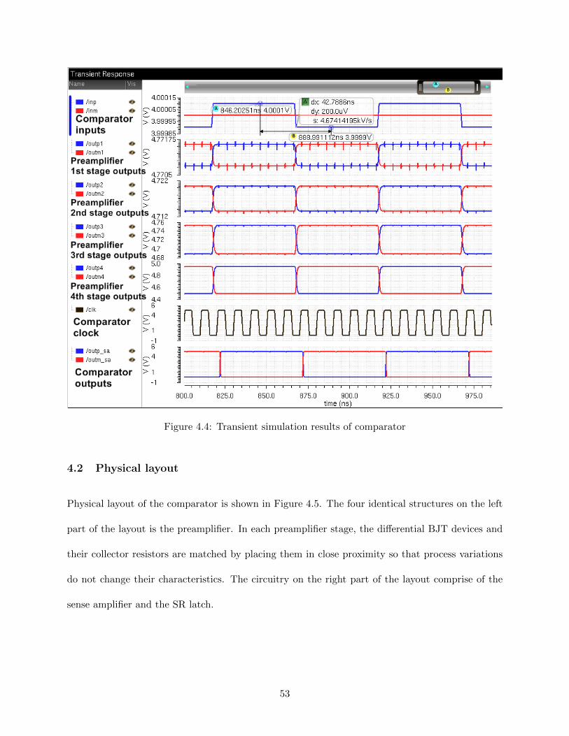
Figure 4.4: Transient simulation results of comparator
4.2 Physical layout
Physical layout of the comparator is shown in Figure 4.5. The four identical structures on the left
part of the layout is the preamplifier. In each preamplifier stage, the differential BJT devices and
their collector resistors are matched by placing them in close proximity so that process variations
do not change their characteristics. The circuitry on the right part of the layout comprise of the
sense amplifier and the SR latch.
53

Figure 4.5: Physical layout of comparator
4.3 Analysis
Figure 4.6 shows the waveforms in a generic transient response of the comparator. This can be
used to understand the operation and factors influencing its performance. The voltage levels of
signals are indicated on the left edge next to the y-axis. The signals are named on the right edge
next to the corresponding waveform.
time
CLK
OUTP
OUTM
INMINP
VDD
0
VCM
VDD
0
tp ts
va
Figure 4.6: Comparator waveforms. Time intervals not to scale
Since the comparator is triggered on the rising edge of clock, there are time limitations on the
signal before and after it for proper operation. These are labeled as tp and ts in the figure. They
54

correspond to preamplifier delay and sense amplifier with latch delay respectively. For the input
change to be seen and responded by the comparator, it must be a time interval tp before the rising
edge of clock. This is the time taken for the signal to propagate through the preamplifier to reach
the sense amplifier inputs. After the clock rising edge, the sense amplifier with latch takes a time
ts to make the decision, latch to the states and drive the outputs. These time durations vary
and depend on factors such as difference between input signals (seen as va in the figure). These
factors are explained along with description and analysis of comparator sub-blocks in the following
sections.
4.3.1 Preamplifier
The preamplifier increases difference between input voltages so that the sense amplifier can detect
and resolve the difference easily and quickly. The preamplifier consists of four cascaded stages of
similar BJT differential amplifiers as shown in Figure 4.2. BJT based amplifiers are used instead
of MOSFET based since the BJTs available in the fabrication process are HBTs (Heterojunction
Bipolar Transistors) which are very high speed devices and result in lower comparator delay.
To analyze the preamplifier, a single unit differential amplifier is considered as shown in Fig-
ure 4.7. This is called the long tailed pair.
DC analysis
The biasing of the differential amplifier must ensure the BJT devices must operate in forward-active
region and not in saturation region for any values of input voltages. In the BJT forward-active
region of operation, the base-emitter junction is forward biased and the base-collector junction is
reverse biased. In BJT saturation region, the base takes considerably higher amount of current
since the beta value (current gain) of the transistor drops significantly. It is important for the base
55

VDD
Q1 Q2INP INM
14kΩ
2kΩ
OUTPOUTM
area = 0.8 µm2
vEvBE1 vBE2
RC1 RC2
REE
Figure 4.7: Unit stage of preamplifier
to take minimal current because the DAC output would be connected here as shown in Figure 2.8
and current drawn from the DAC results in proportional error in the DAC output value as explained
later in Chapter 5. In the saturation region, the collector-base junction is forward biased. The
values of collector and emitter resistors RC1, RC2 and REE are chosen to prevent this. The worst
case situation for this to happen is when one input is V DD and the other input is ground since
only one branch is turned on completely and the collector voltage has the possibility to be pulled
to the lowest voltage. Assuming this condition of INP = VDD and INM = 0. Also assuming VCE
of the BJT to be zero which would again be a pessimistic assumption. Now, the voltage on the
collector is seen to be a divided voltage between RC1 and REE . This is given as,
VC1 = VOUTM =V DD ·REE
RC1 +REE=
5 · 14× 103
2× 10³ + 14× 103= 4.375 V (4.1)
Now, the base is at VDD = 5 V. Therefore, the voltage across the collector-base PN junction would
be,
VBC = VB − VC = 5− 4.375 = 0.625 V (4.2)
56

This voltage is lower than the needed forward cutoff voltage of 0.7 V for the collector-base PN
junction. As a result, the BJTs would not go into saturation. This value is worst-case since the
BJT VCE voltage would add to this. To have a higher margin for not moving into the saturation
region, the value of REE could be increased or the value of RC could be reduced slightly.
The voltage calculated in Equation (4.1) is the minimum voltage reached by the collector node.
The maximum voltage reached by the collector is VDD when the corresponding branch is off and
the output is pulled high by the collector resistor. As a result, the single-ended output voltage
range of the circuit is from 4.375 V to 5 V assuming negligible VCE .
The minimum input voltage needed for operation is slightly above the threshold voltage value
of about 0.7 V. Therefore, the input voltage range is 0.7 V to 5 V. This voltage range matches the
output range of TIA.
This differential amplifier increases the small difference between input signals. However, the
absolute voltage values of each signal input into INP and INM could be high. The common value of
both inputs is called the common-mode voltage VCM . The signal difference level rides on top of the
common-mode voltage. For example, if INP = 3.0 V and INM = 3.1 V, them the common-mode
voltage is 3.05 V and the input difference voltage is 100 mV.
The output of the differential amplifier is the difference between the two output voltages OUTP
and OUTM. But they can have a large common-mode voltage level. This can be defined as VOUTP =
VOUTM = VCM,out. This output common-mode voltage depends on the input common-mode voltage
and can be calculated as follows. This calculation assumes VINP = VINM = VCM,in. The calculation
is shown for the left side branch. The same applies to the right side branch. The voltage on emitter
node, VE is the voltage drop across the emitter resistor due to currents from both branches.
VE = 2 · IC ·REE (4.3)
57
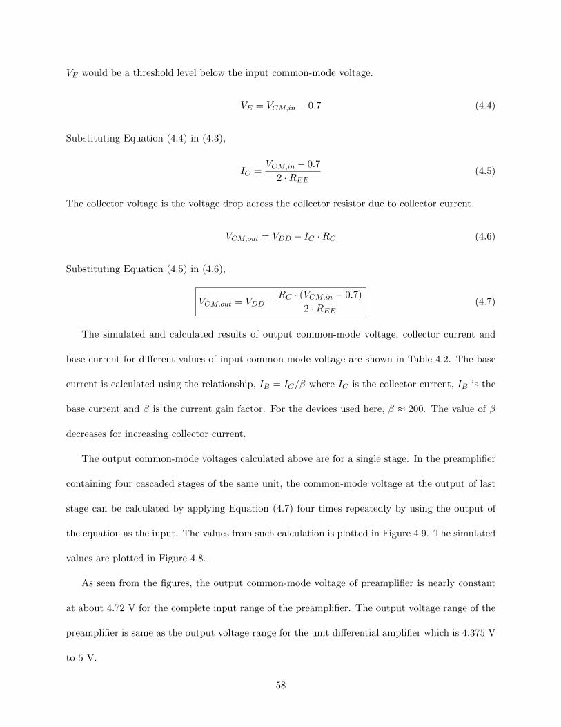
VE would be a threshold level below the input common-mode voltage.
VE = VCM,in − 0.7 (4.4)
Substituting Equation (4.4) in (4.3),
IC =VCM,in − 0.7
2 ·REE(4.5)
The collector voltage is the voltage drop across the collector resistor due to collector current.
VCM,out = VDD − IC ·RC (4.6)
Substituting Equation (4.5) in (4.6),
VCM,out = VDD −RC · (VCM,in − 0.7)
2 ·REE(4.7)
The simulated and calculated results of output common-mode voltage, collector current and
base current for different values of input common-mode voltage are shown in Table 4.2. The base
current is calculated using the relationship, IB = IC/β where IC is the collector current, IB is the
base current and β is the current gain factor. For the devices used here, β ≈ 200. The value of β
decreases for increasing collector current.
The output common-mode voltages calculated above are for a single stage. In the preamplifier
containing four cascaded stages of the same unit, the common-mode voltage at the output of last
stage can be calculated by applying Equation (4.7) four times repeatedly by using the output of
the equation as the input. The values from such calculation is plotted in Figure 4.9. The simulated
values are plotted in Figure 4.8.
As seen from the figures, the output common-mode voltage of preamplifier is nearly constant
at about 4.72 V for the complete input range of the preamplifier. The output voltage range of the
preamplifier is same as the output voltage range for the unit differential amplifier which is 4.375 V
to 5 V.
58

Input common- Simulated Calculatedmode voltage IC IB VCM,out IC IB VCM,out
VCM,in in volts in µA in nA in volts in µA in nA in volts
1 9.5 18.4 4.98 10.7 53.6 4.981.25 17.7 52.1 4.96 19.6 98.2 4.961.5 26.2 96.4 4.95 28.6 142.9 4.941.75 34.7 146.6 4.93 37.5 187.5 4.93
2 43.4 199.4 4.91 46.4 232.1 4.912.25 52.0 252.6 4.90 55.4 276.8 4.892.5 60.7 305.1 4.88 64.3 321.4 4.872.75 69.4 356.4 4.86 73.2 366.1 4.85
3 78.1 406.7 4.84 82.1 410.7 4.843.25 86.8 456.1 4.83 91.1 455.4 4.823.5 95.5 505.2 4.81 100.0 500.0 4.803.75 104.3 554.2 4.79 108.9 544.6 4.78
4 113.0 603.4 4.77 117.9 589.3 4.764.25 121.8 653.0 4.76 126.8 633.9 4.754.5 130.6 703.0 4.74 135.7 678.6 4.734.75 139.3 753.3 4.72 144.6 723.2 4.71
5 148.0 804.2 4.70 153.6 767.9 4.69
Table 4.2: Output common-mode voltage, collector and base currents for preamplifier single stageat different input common-mode voltages
AC gain analysis
The AC gain of the preamplifier is defined as the change in output voltage difference (VOUTP −
VOUTM ) to the change in input voltage difference (VINP − VINM ). The AC gain is a measure of
the sensitivity of the preamplifier.
To analyze the AC small-signal gain of the preamplifier, again consider the preamplifier unit
stage shown in Figure 4.7. Initially, consider both input voltages VINP and VINM are at the same
common-mode voltage. The difference between input voltages is zero. The outputs VOUTP and
VOUTM would be at the corresponding common-mode voltages as explained in the previous section.
The output voltage difference is zero. Now, if one input is held constant and the other input changes
by a small amount, this is called single-ended mode of operation. If both inputs move in opposite
directions by small amount, this is called the differential input mode.
59

Figure 4.8: Simulation of output common-mode voltage vs input common-mode voltage forpreamplifier
(10*
vcm
+181
0627
)/38
4160
vcm
4.71322
4.71324
4.71326
4.71328
4.7133
4.71332
4.71334
4.71336
1 1.5 2 2.5 3 3.5 4 4.5 5
Figure 4.9: Calculation of output common-mode voltage vs input common-mode voltage forpreamplifier
In single-ended mode of operation, lets say VINP and VINM are at the same voltage initially.
Then, VINP increases by ∆V . This results in the collector current of Q1 increase by ∆IC . This
leads to a higher voltage drop across the emitter resistor which increases voltage vE . As a result,
the base to emitter voltages, vBE1 and vBE2 both decrease. The voltage vE reaches a value such
that the increase in input voltage ∆V is split equal and opposite between vBE1 and vBE2 so that
collector current change for both Q1 and Q2 are equal and opposite [17, p. 625]. This can be
described in small-signal sense considering VINM to be AC ground as,
vbe1 = −vbe2 =vin2
(4.8)
In differential mode of operation, lets say VINP and VINM are at the same voltage initially. Then
if VINP increases by ∆V and VINM decreases by ∆V , the differential input voltage is VINP−VINM =
2 ·∆V . In this case, since both inputs change in equal and opposite amounts, the voltage vE stays
constant [17, p. 624].
In the preamplifier, the first stage operates in single-ended input mode since one input is con-
nected to the DAC output and other input is connected to the TIA output which varies based on
the photodetector output.
60

It is important that the devices Q1 and Q2, RC1 and RC2 be matched as closely as possible.
Mismatches lead to input offset voltages and currents. To match these devices, care has been taken
in layout but there would still be random process variations which might cause mismatch and limit
the offset performance of the preamplifier.
In both single-ended and differential input modes, the differential amplifier can be analyzed as
the equivalent circuit seen in Figure 4.10 because the input is split equally between both sides as
explained earlier.
VDD
Q3
2kΩRC
OUT
IN
Figure 4.10: Equivalent circuit for gain calculations
In Figure 4.10, to analyze the small-signal gain, consider the device Q3 is operating in active
region. Q3 appears like a small-signal voltage controlled current source with transconductance gm.
VDD can be considered as small-signal ground. The AC collector current is given by,
ic = gm · vbe (4.9)
Voltage drop across the collector resistor is equal to output voltage which can be expressed as,
vout = −ic ·RC (4.10)
The small-signal gain can be calculated by substituting Equation (4.9) in Equation (4.10). Also
61

note that vbe = vin since the emitter is ground in this equivalent circuit.
A =voutvin
= −gm ·RC (4.11)
The gain of the preamplifier unit stage at each input common-mode voltage is shown in Table 4.3.
The values of gm were measured in simulation at the input common-mode voltage operating point.
The gm of BJT is proportional to the collector current which is a function of input common-mode
voltage.
Input common- Transconductance Simulated Calculatedmode voltage (gm) in mA/V gain gain
0.75 0.08 -0.15 -0.161 0.36 -0.68 -0.72
1.25 0.67 -1.27 -1.341.5 0.99 -1.86 -1.981.75 1.31 -2.45 -2.62
2 1.63 -3.04 -3.262.25 1.95 -3.63 -3.902.5 2.27 -4.21 -4.542.75 2.59 -4.78 -5.18
3 2.91 -5.36 -5.823.25 3.23 -5.92 -6.463.5 3.54 -6.48 -7.083.75 3.86 -7.04 -7.72
4 4.17 -7.59 -8.344.25 4.49 -8.13 -8.984.5 4.80 -8.67 -9.604.75 5.11 -9.21 -10.22
5 5.42 -9.73 -10.84
Table 4.3: Preamplifier single stage gain at different input common-mode voltages
The cascaded gain of the complete preamplifier would be the product of individual gains of
each stage. Since the gain depends on the value of input common-mode voltage, the latter must
be calculated at the input of each stage using Equation (4.7). The gain for corresponding input
common-mode voltages are interpolated using the values in Table 4.3. The total gain values are
tabulated in Table 4.4. In this table, A1, A2, A3 and A4 represent the individual gain values
of the four stages. VCM,in2, VCM,in3 and VCM,in4 are the common-mode voltages at the inputs
62
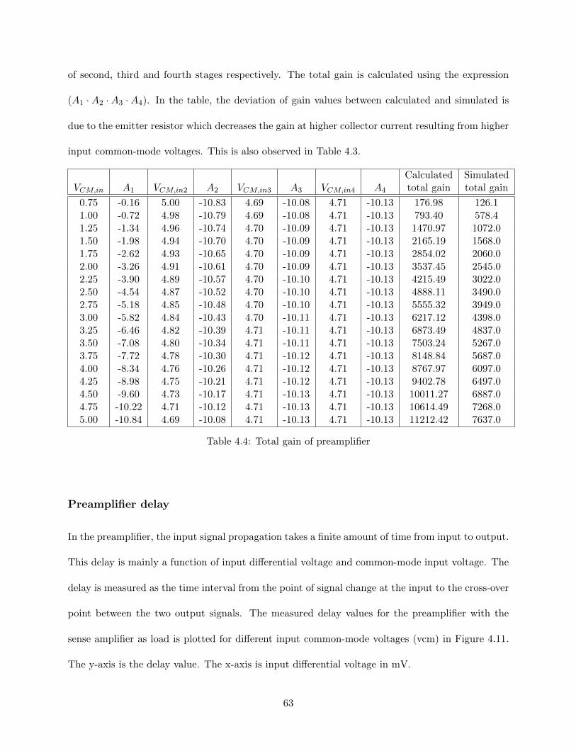
of second, third and fourth stages respectively. The total gain is calculated using the expression
(A1 ·A2 ·A3 ·A4). In the table, the deviation of gain values between calculated and simulated is
due to the emitter resistor which decreases the gain at higher collector current resulting from higher
input common-mode voltages. This is also observed in Table 4.3.
Calculated SimulatedVCM,in A1 VCM,in2 A2 VCM,in3 A3 VCM,in4 A4 total gain total gain
0.75 -0.16 5.00 -10.83 4.69 -10.08 4.71 -10.13 176.98 126.11.00 -0.72 4.98 -10.79 4.69 -10.08 4.71 -10.13 793.40 578.41.25 -1.34 4.96 -10.74 4.70 -10.09 4.71 -10.13 1470.97 1072.01.50 -1.98 4.94 -10.70 4.70 -10.09 4.71 -10.13 2165.19 1568.01.75 -2.62 4.93 -10.65 4.70 -10.09 4.71 -10.13 2854.02 2060.02.00 -3.26 4.91 -10.61 4.70 -10.09 4.71 -10.13 3537.45 2545.02.25 -3.90 4.89 -10.57 4.70 -10.10 4.71 -10.13 4215.49 3022.02.50 -4.54 4.87 -10.52 4.70 -10.10 4.71 -10.13 4888.11 3490.02.75 -5.18 4.85 -10.48 4.70 -10.10 4.71 -10.13 5555.32 3949.03.00 -5.82 4.84 -10.43 4.70 -10.11 4.71 -10.13 6217.12 4398.03.25 -6.46 4.82 -10.39 4.71 -10.11 4.71 -10.13 6873.49 4837.03.50 -7.08 4.80 -10.34 4.71 -10.11 4.71 -10.13 7503.24 5267.03.75 -7.72 4.78 -10.30 4.71 -10.12 4.71 -10.13 8148.84 5687.04.00 -8.34 4.76 -10.26 4.71 -10.12 4.71 -10.13 8767.97 6097.04.25 -8.98 4.75 -10.21 4.71 -10.12 4.71 -10.13 9402.78 6497.04.50 -9.60 4.73 -10.17 4.71 -10.13 4.71 -10.13 10011.27 6887.04.75 -10.22 4.71 -10.12 4.71 -10.13 4.71 -10.13 10614.49 7268.05.00 -10.84 4.69 -10.08 4.71 -10.13 4.71 -10.13 11212.42 7637.0
Table 4.4: Total gain of preamplifier
Preamplifier delay
In the preamplifier, the input signal propagation takes a finite amount of time from input to output.
This delay is mainly a function of input differential voltage and common-mode input voltage. The
delay is measured as the time interval from the point of signal change at the input to the cross-over
point between the two output signals. The measured delay values for the preamplifier with the
sense amplifier as load is plotted for different input common-mode voltages (vcm) in Figure 4.11.
The y-axis is the delay value. The x-axis is input differential voltage in mV.
63

Figure 4.11: Plot of preamplifier delay for different values of input common-mode voltage. X-axisis in mV
As seen from Table 4.4, the cascaded gain of preamplifier increases with increase in input
common-mode voltage. This is also reflected in the plot in Figure 4.11 where the higher input
common mode voltage curves have lesser delay for the same input differential voltage. A higher
input differential voltage also results in lesser delay due to larger resulting currents that charge
the internal capacitances faster. To reduce the delay, we could increase the bias current in the
differential amplifiers. We could also reduce the number of differential amplifier stages but that
would reduce the sensitivity to input differential voltages.
The plot shown in Figure 4.11 is from simulations of pre-layout schematics without considering
parasitics of on-chip wiring. The delay can be expected to increase with post-layout simulations
including on-chip parasitics.
4.3.2 Sense amplifier and latch
The sense amplifier and latch which are the second and third stages respectively of the comparator
are explained and analyzed in this section.
64

Sense amplifier
Figure 4.12 shows the sense amplifier which is the second stage of the comparator. The sense
amplifier takes the outputs from preamplifier, compares them and latches onto the decision of
which signal is higher and lower. When INP is higher than INM, the outputs OUTP_SA goes
high and OUTM_SA goes low on the rising edge of clock (CLK) and vice versa. When clock goes
low, irrespective of the input voltages, both outputs OUTP_SA and OUTM_SA go high. This is
represented in Table 4.5. In the first two rows of the table, the input voltages are represented as
a small change in voltage ∆V riding on a common-mode voltage VCM . The two inputs have the
same VCM but opposite change in ∆V .
W=5uL =0.5u
MP3pmos
W=3uL =0.5u
MN2nmos
W=5uL =0.5u
MP2pmos
W=5uL =0.5u
MP4pmos
W=5uL =0.5u
MP1pmos
W=3uL =0.5u
MN1nmos
W=3uL =0.5u
MN4nmos
W=3uL =0.5u
MN3nmos
W=3uL =0.5u
MN6nmos
W=3uL =0.5u
MN5nmos
VDD
CLK
INP
INM
OUTP_SA
OUTM_SA
Figure 4.12: Sense amplifier
INP INM CLK OUTP_SA OUTM_SA
VCM + ∆V VCM −∆V 1 0
VCM −∆V VCM + ∆V 0 1
× × 0 1 1
Table 4.5: Characteristic table of sense amplifier
65

The sense amplifier operation can be understood as follows. When clock is low, the devices MN1
and MN2 are off and devices MP1 and MP4 are on. This results in OUTP_SA and OUTM_SA
pulled high. The capacitance at OUTP_SA and OUTM_SA are charged to VDD. This also turns
off the devices MP2 and MP3. However, this turns on the devices MN3 and MN4. Therefore,
irrespective of the value of input voltages, the outputs are pulled high until clock is low. Now, lets
consider INP is slightly higher than INM. When clock goes high, the drain current through MN6
would be slightly higher than through MN5. The capacitance at OUTP_SA and OUTM_SA which
would be initially charged to VDD start discharging through the pull-down NMOS devices in each
branch. The discharge rates in each branch would be different due to the mismatch in currents.
The capacitance on node OUTM_SA would discharge at a faster rate than OUTP_SA. Now, the
devices MP2 and MP3 start to turn-on. Since OUTM_SA discharges faster than OUTP_SA, MP2
turns on faster than MP3. Due to these actions, the pull-down current is greater than pull-up
current on OUTM_SA and the pull-up current is greater than pull-down current on OUTP_SA.
There is positive feedback action in the circuit where the voltage on OUTP_SA and OUTM_SA
regenerate until they snap and reach VDD or ground depending on the initial discharge rates in
both branches. This latching action is due to the cross connected gates of the PMOS and NMOS
devices which has a stable memory state.
For proper operation, the inputs must be higher than the threshold voltage of the input NMOS
devices when clock is high. This is so that a pull-down path is present to drive logic levels on the
output of the sense amplifier.
The sense amplifier is edge triggered because, when the clock signal is high and past the rising
edge, any change in input would be overpowered by the latched positive feedback action which
maintains the same value.
Since the sense amplifier outputs OUTP_SA and OUTM_SA go high when the clock is low,
66

this is not the final comparator output. The comparator characteristics dictate the output to stay
constant when the input voltages are constant. Therefore, an SR latch is added to the output of
sense amplifier so that the previous output is held latched as the comparator output when the clock
goes low. The SR latch is explained in the next section.
Figure 4.13 shows the plot of delay of the cascade of sense amplifier and latch where sense
amplifier delay is in y-axis and the input differential voltage is on the x-axis. A load capacitance
of 50 fF is placed on the output of latch to emulate the input capacitance of the input-output
(IO) circuit which is used to drive the comparator output signal off-chip. The profile of the plot
indicates the delay characteristics of the sense amplifier since the delay of latch is constant as it
is a digital circuit connected to the digital output of the sense amplifier. The delay values in the
plot was measured in simulation by measuring the time interval from the rising edge of clock to the
comparator output transition for different values of input differential voltage and common-mode
voltage.
Figure 4.13: Plot of sense amplifier and latch delay vs input differential voltage. X-axis is in mV
67

As seen from the plot, the delay decreases for higher values of input differential voltage. The
delay also varies with respect to the input common-mode voltage. To understand the delay char-
acteristics of the sense amplifier, lets consider a single NMOS pull-down branch. This is seen in
Figure 4.14.
The circuit in Figure 4.14 emulates the pull-down action that happens just after the rising edge
of clock. At this time, the outputs would be charged to VDD which is shown in the circuit as the
drain of MN2. The gate of MN2 is connected to clock in the sense amplifier which is also tied to
VDD in this circuit. The gate of MN4 would be connected to the complementary output of the
sense amplifier. This would also be initially charged to VDD and the same is replicated in this
circuit. This circuit can be used to analyze the pull-down current with varying input voltage.
W=3uL =0.5u
MN2nmos
W=3uL =0.5u
MN4nmos
W=3uL =0.5u
MN6nmos
VDD
VDD
VDD
iPD
+−
vIN
Figure 4.14: Pull-down circuit of one half ofsense amplifier
Figure 4.15: Derivative of pull-down current versus input voltage(∂iPD∂vIN
= Transconductance)
of the circuit
in Figure 4.14
The plot in Figure 4.15 shows the transconductance of the pull-down circuit. That is the
incremental ratio of pull-down current to input voltage. This gives a measure of the current
difference in both branches of the sense amplifier for a small difference between both input voltages
riding on a common-mode voltage. We can see that for input common-mode voltages lower than
68

the threshold voltage of the NMOS, no current flows. The transconductance rapidly increases after
that and reaches a peak and reduces again. The region of high transconductance is when the
input NMOS devices (MN5 and MN6) are in saturation. At higher values of input common-mode
voltages, these devices operate in linear region which reduces the transconductance.
The transconductance of pull-down circuit decreases at high common-mode voltages because
the input NMOS devices go into triode region of operation and the drain current does not increase
with increase in gate to source voltages.
Decrease in transconductance of the pull-down circuit increases delay because the OUTP_SA
and OUTM_SA nodes take more time to reach the switching point. This is because the pull-
up current from the PMOS devices would be equal to the pull-down current from the NMOS
devices. As a result, there would be less excess current to charge the capacitances at OUTP_SA
and OUTM_SA which would result in more time to reach the switching point.
Since the common-mode output voltage of the preamplifier is about 4.71 V as shown in Fig-
ure 4.8, this point lies on the transconductance curve of the pull down network as marked in the
Figure 4.15. The corresponding delay curve can be seen in the delay plot to be within the group
of curves for 5V > VCM ≥ 2V . Even though this point does not lie on the high transconductance
region of the curve, the sense amplifier sensitivity is not significantly affected as seen in the delay
curve. The delay values of the sense amplifier and latch with an input common-mode voltage of
4.71 V are tabulated in Table 4.6.
The maximum frequency of clock this comparator operates at is limited by the sense amplifier
delay time since the preamplifier delay is much less than the sense amplifier delay in all conditions.
A clock with a period which is twice or higher than the maximum sense amplifier delay would
ensure the sense amplifier output is available before the falling edge of the clock. The maximum
delay value of the sense amplifier from Table 4.6 is 1.887 ns. As a result, the maximum clock input
69

Input differential Delayvoltage in mV in ns
0.1 1.8870.2 1.8310.5 1.7531 1.6912 1.6275 1.5427 1.51110 1.477
Table 4.6: Delay of sense amplifier and latch for input common-mode voltage of 4.71 V from thepreamplifier
frequency would be about 265 MHz .
The sense amplifier also has kickback noise on the inputs due to the snap operation at each
clock edge. The voltages on the drain of input NMOS devices MN5 and MN6 change at every rising
and falling edge of clock. This gets coupled onto the input of comparator through the input NMOS
devices’ drain to gate capacitance. This capacitively couples back through the preamplifier which
can be seen as short glitches on the output of each stage of the preamplifier at rising and falling
edges of clock.
The values plotted in Figure 4.13 are from simulations of pre-layout schematics which does not
consider parasitics of on-chip wiring. The delay can be expected to increase with post-layout netlist
simulations.
The sense amplifier with latch could be used as a standalone comparator but the addition
of preamplifier on the front-end increases sensitivity to smaller input differences. However, the
preamplifier introduces the constraint of a setup time before the rising edge of the clock when the
input voltages need to be stable. Also, the preamplifier might have input voltage offset due to
device mismatch and the sensitivity is ultimately determined by this.
70

SR Latch
Figure 4.16 shows the SR latch which is the third stage of the comparator. The SR latch is imple-
mented using 2-input NAND gates. The schematic of 2-input NAND gate is seen in Figure 4.17.
As eluded to in the previous section, the latch keeps the output of sense amplifier constant when
clock goes low.
Q
Q
S
R
Figure 4.16: Schematic of SR latch
VDD VDD
A
B
Y
Figure 4.17: Schematic of 2-input NAND gateused in SR latch. All PMOS = 5µm/0.5µm. AllNMOS = 4µm/0.5µm
From the truth table of 2-input NAND gate in Table 4.7, we can infer two key properties of
the NAND gate. Firstly, when any of the input is high, the other input to output has the logic
relationship of an inverter. Secondly, the output of NAND gate goes high when either of its input
is low. From the first property, we can see that when both inputs to the latch are high, the circuit
behaves as two inverters connected in anti-parallel. This is a memory device that has two stable
logic states of high or low. As a result, when both inputs to the SR latch go high, the previous logic
state is held in the latch. From the second property of the NAND gate, we can see that whichever
input is pulled low, the corresponding output goes high.
The characteristic table of the latch seen in Table 4.8 shows the behavior of the SR latch for
all combinations of inputs. These characteristics directly follow from the properties of the NAND
71

A B Y
0 0 10 1 11 0 11 1 0
Table 4.7: Truth table of 2-input NAND gate
gate explained above. When the S (set) input is high and R (reset) is low, the output Q goes high
and Q goes low. Similarly, when the R (reset) input is high and S (set) input is low, the output Q
goes low and Q goes high. We can see that the output Q follows the set input if the reset input
is its complement. When both inputs to the SR latch go low, both outputs go high which is an
invalid state since the outputs Q and Q must be complementary for proper operation.
S R Q Q
0 0 1 10 1 0 11 0 1 0
1 1 Qprev Qprev
Table 4.8: Characteristic table of SR latch
The latch shown in Figure 4.16 is connected to the output of the sense amplifier. OUTP_SA from
sense amplifier is connected to the S input of latch. OUTM_SA of sense amplifier is connected to
the R input. Q and Q are the OUTP and OUTM outputs of the comparator. Therefore, comparing
Tables 4.5 and 4.8, we can see that the latch stores the output of sense amplifier when clock is low
and give the right output when clock is high. Since the sense amplifier outputs never both go low
at the same time, the invalid state is never reached.
72

Chapter 5
R-2R Digital-to-Analog Converter
(DAC)
As described in Chapter 2, the discrete return LiDAR needs a reference voltage for the comparator
to set the trigger threshold so that the incoming signal is recovered above the ambient level.
The reference voltage could be set externally using off-chip components but in order to have an
integrated single chip solution, a Digital-to-Analog converter (DAC) is implemented on the same
chip. The DAC is a device that generates analog output quantity (voltage or current) proportional
to input digital code. This provides digital control of the trigger level making it robust and reduces
variations. This chapter describes the design and implementation details of an R-2R DAC.
The DAC topology chosen here is R-2R ladder type [13, p. 1024]. This is a simple and popular
topology but is also versatile. Part of the versatility is because it is easily extensible to any
resolution, provided the components used (resistors) have a tight tolerance and are matched enough.
The DAC implemented here has a resolution of 10-bits. It is a serial digital input DAC. It has an
adjustable output range. These features are described later.
The DAC designed was chosen to have a 10-bit resolution because fine control of output voltage
73

is needed for the intended application. Setting the trigger level at the right value just above ambient
level is important and can be the difference between capturing or missing the incoming signal.
The DAC can be configured in voltage-mode or current-mode [13, p. 1028,1039]. In the voltage-
mode without using external opamp, the DAC output can only drive high-impedance loads meaning
that it cannot drive higher currents. The amount of loading impacts accuracy as described later
in Section 5.4.3. As shown in the discrete return LiDAR block diagram Figure 2.8, the DAC is
driving input of the comparator which is a high impedance input. So, in this application, the DAC
is used in voltage-mode without opamp. The DAC can be configured in the current-mode using an
external opamp if needed to drive higher currents.
The chapter is organized as follows. Firstly, the ideal DAC characteristics, specifications and
nonlinearities are described. Next, the R-2R DAC is explained. Next, simulation results and
physical layout of the R-2R DAC are shown. Then, the implementation details and considerations
for the R-2R DAC are discussed.
5.1 Ideal DAC
An ideal DAC would have the transfer curve as seen in Figure 5.1 [13, p. 940]. This is an example of
a 3-bit DAC. The x-axis represents input digital code and y-axis represents output analog voltage.
The transfer curve is discrete due to the input being a digital number. For an increase of 1 bit in
the input digital code, the output voltage changes by 1 LSB = V DD/(2N ) where LSB stands for
Lowest Significant Bit and N is the number of bits in the DAC.
The DC linearity parameters of a DAC are the differential non-linearity (DNL), integral non-
linearity (INL), gain error and offset error. These parameters quantify the amount and type of
deviation of DAC output DC characteristics compared to ideal characteristics.
74

Figure 5.1: Ideal DAC characteristics for 3-bit DAC
5.2 DAC Linearity
A real DAC has many sources of errors and nonlinearities. These arise due to resistor mismatches,
switch resistances, output load, dynamic effects etc. The following sections describe the DC non-
linearities: DNL, INL, gain error and offset error.
5.2.1 DNL
The differential non-linearity (DNL) of a DAC is defined as the difference between actual step size
and ideal step size of the output voltage in the transfer curve for every digital code of the DAC.
This is represented in Figure 5.2 [13, p. 941]. The DNL of a DAC is measured in terms of LSBs
instead of voltage values to make the specification independent of resolution of a particular DAC.
For example, a DAC having 0.1 LSB of DNL error is considered good performance regardless of the
resolution of the DAC. 0.1 LSB translates to different voltage values for different resolution DACs.
The ideal step size of a DAC is 1 LSB. The DNL for every step or digital input code is calculated
75

Figure 5.2: Measuring DAC DNL
using Equation (5.1) where n represents each digital code.
DNLn = (actual step size)n − (ideal step size)
= (actual step size)n − 1 LSB
(5.1)
Monotonicity is an important property of DACs. This means for every increase in input digital
code, the output voltage of the DAC must increase and not decrease. This would not be the case if
the DNL for any digital code is less than 1 LSB, and the output voltage would make a step down in
the transfer curve for an increase in the input digital code. This behavior is undesirable especially
when the DAC is used as part of a feedback loop for example in a successive approximation ADC.
For a DAC to be monotonic and be considered N-bit accurate the DNL must be within ±1/2 LSB
[13, p. 943].
5.2.2 INL
The integral non-linearity (INL) of a DAC is defined as the difference between actual output
voltage and a reference straight line drawn between the endpoints of the DAC transfer curve. This
76

is represented in Figure 5.3 [13, p. 943]. Similar to DNL, the INL of a DAC is also measured in
units of LSBs. An N-bit DAC is usually expected to have INL within ±1/2 LSB [13, p. 943].
Figure 5.3: Measuring DAC INL
INL is given by Equation (5.2) where n represents each digital code.
INLn = (actual output voltage)n − (value of reference line)n (5.2)
There is an alternate technique for measuring INL called the best straight-line fit INL method
[13, p. 945] [18]. In this method, the reference line is not drawn joining the end-points of the
transfer curve, rather the line is drawn so as to reduce the INL values. If the transfer curve of the
DAC is like an arc, then the reference line is drawn to lie on the middle of the arc so that there is
same maximum deviation of samples on either side of the reference line. This way of defining INL
reduces the INL numbers but compensates for it as gain and offset errors (described next).
77

5.2.3 Gain Error
The gain error of a DAC is the deviation of the slope of the transfer curve compared to ideal slope
[13, p. 945]. Figure 5.4 [13, p. 946] shows the gain error in DAC transfer characteristics. Gain error
is given by equation (5.3) [13, p. 945]. It can be expressed in units of LSB/bit. Increase in gain
error also affects DNL but is divided among all the bits.
Gain error = Ideal slope− actual slope (5.3)
Figure 5.4: Gain error of DAC
5.2.4 Offset Error
The offset error of a DAC is defined as the DAC output voltage at digital input code of zero. Ideally,
the DAC output voltage must be VREF− at a code of zero but can be different due to non-idealities.
Figure 5.5 [13, p. 945] shows the offset error in DAC transfer characteristics.
78

Figure 5.5: Offset error of DAC
5.3 R-2R DAC
Operation and design of the R-2R based DAC are described in the sections below:
5.3.1 Basic voltage-mode R-2R DAC
The circuit diagram of an ideal 10-bit R-2R DAC is shown in Figure 5.6. The inputs b9, . . . , b0
are the digital input code, VREF+ and VREF− are the reference voltages and VOUT is the output
voltage. The main components of an R-2R DAC are the resistors. The resistor values used are R
and 2R. In the circuit, the resistors are arranged such that they form successive voltage dividers
along the ladder. The voltage dividers are formed with the input resistor for every bit along with
the rest of the network. The voltage division ratio for each bit is 1/2p where p is the position of the
bit. For the 10-bit DAC designed here, p = 9 for MSB and p = 0 for LSB. This operation weights
the bits in powers of 2 according to their positions. MSB has the highest weight and LSB has the
lowest. The resistor ladder input close to VOUT is the MSB and the farthest input is the LSB. This
79

results in an output voltage that is an analog representation of the digital input.
2R
R
2R
R
2R
R
2R
R
2R
R
2R
R
2R
R
2R
R
2R
R
2R
VOUT
MSBLSB
2R
VREF+
VREF–
VREF–
b9b8b7b6b5b4b3b2b1b0
1 0 01 01 01 01 01 01 01011 0
Figure 5.6: Basic voltage-mode R-2R DAC
This operation is represented mathematically in equation (5.4) [13, p. 1025].
VOUT =b9 · VREF+ + b9 · VREF−
2+b8 · VREF+ + b8 · VREF−
4+b7 · VREF+ + b7 · VREF−
8
+b6 · VREF+ + b6 · VREF−
16+b5 · VREF+ + b5 · VREF−
32+b4 · VREF+ + b4 · VREF−
64
+b3 · VREF+ + b3 · VREF−
128+b2 · VREF+ + b2 · VREF−
256+b1 · VREF+ + b1 · VREF−
512
+b0 · VREF+ + b0 · VREF−
1024
(5.4)
In this equation, b9, . . . , b0 represent the input digital code and can take values of 0 or 1 with
b9 and b0 being the MSB and LSB respectively. The reference voltages VREF+ and VREF− affect
the output voltage range. For a given VREF+ and VREF−, sweeping the input codes from all zeros
to all ones makes the output go from (VREF−) to (VREF+ − 1 LSB) where an LSB is the minimum
step size of the output voltage as shown in Figure 5.1. An LSB is given by equation (5.5) where N
is the resolution of DAC.
1 LSB =VREF+ − VREF−
2N(5.5)
Its important to reiterate that VREF+ and VREF− directly affect the accuracy of the DAC.
In this discussion, the switches operated by the input bits are considered ideal and do not have
resistance. The effect of real switch with resistance is considered later in Section 5.4.4.
80
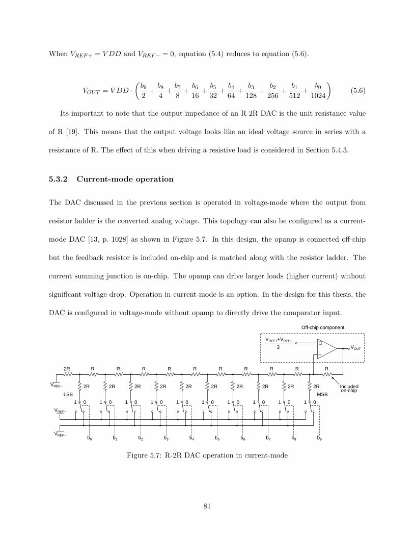
When VREF+ = V DD and VREF− = 0, equation (5.4) reduces to equation (5.6).
VOUT = V DD ·(b92
+b84
+b78
+b616
+b532
+b464
+b3
128+
b2256
+b1
512+
b01024
)(5.6)
Its important to note that the output impedance of an R-2R DAC is the unit resistance value
of R [19]. This means that the output voltage looks like an ideal voltage source in series with a
resistance of R. The effect of this when driving a resistive load is considered in Section 5.4.3.
5.3.2 Current-mode operation
The DAC discussed in the previous section is operated in voltage-mode where the output from
resistor ladder is the converted analog voltage. This topology can also be configured as a current-
mode DAC [13, p. 1028] as shown in Figure 5.7. In this design, the opamp is connected off-chip
but the feedback resistor is included on-chip and is matched along with the resistor ladder. The
current summing junction is on-chip. The opamp can drive larger loads (higher current) without
significant voltage drop. Operation in current-mode is an option. In the design for this thesis, the
DAC is configured in voltage-mode without opamp to directly drive the comparator input.
2R
R
2R
R
2R
R
2R
R
2R
R
2R
R
2R
R
2R
R
2R
R
2R
VOUT
MSBLSB
2R
VREF+
VREF–
VREF–
b9b8b7b6b5b4b3b2b1b0
1 0 01 01 01 01 01 01 01011 0
−
+
R
VREF++VREF-
2
Includedon-chip
Off-chip component
Figure 5.7: R-2R DAC operation in current-mode
81

5.3.3 R-2R DAC schematic
The DAC schematics discussed above use ideal switches with no resistances. The schematic in
Figure 5.8 shows the complete circuit diagram of the 10-bit R-2R DAC implemented here. This
circuit is designed in AMS 0.35µm SiGe BiCMOS process. It has some added circuitry. These are
described below.
2R
R
2R
R
2R
R
2R
R
2R
R
2R
R
2R
R
2R
R
2R
R
2R
VOUT
MSBLSB
2R
VREF–
VREF+
VREF–
OEN
Drive inverters
Logic inverters
AND gates
R
RFB
DQ
Q
DQ
Q
DQ
Q
DQ
Q
DQ
Q
DQ
Q
DQ
Q
DQ
Q
DQ
Q
DQ
Q
CLK
DATA IN
R = 13.2 kΩ
D Flip-Flops
Figure 5.8: Complete schematic of R-2R DAC
The switches in the ideal case are replaced by drive inverters with large devices. The devices
are large in width (W/L ratio) to get a low resistance drive of input voltage. The resistance of
switches affect the accuracy of the DAC as discussed later in Section 5.4.4. The drive inverters are
driven by a smaller inverter to complement the logic and give the right output.
The drive inverters are powered by VREF+ and VREF− so that output voltage range can be
varied. For rail-to-rail output voltage range, VREF+ must be connected to VDD and VREF− must
be connected to ground. Details of the drive inverter are discussed in Section 5.4.1.
The D flip-flops enable serial digital input. The string of cascaded flip-flops act as a shift register
82

and clocks in one bit at a time with respect to the rising edge of clock signal. The AND gates are
used to prevent the output of flip-flops going into the resistor ladder when the digital data is being
shifted in to prevent partial data causing erratic output. The AND gates let the data go through
when OEN is asserted high and the data is completely shifted in. This part of the circuitry is
explained in detail in Section 5.4.2.
An on-chip resistor with value R whose one end is connected to VOUT and the other end
connected to a pad RFB is added as shown on the right side of the figure. This is to configure the
DAC for current-mode operation as detailed before.
5.3.4 Simulation results
Simulation results for the DAC design described in the previous section are as follows.
Simulation of DAC output characteristics
Figure 5.9 shows the operation of DAC in voltage mode with VREF+ = 5 V and VREF− = 0 V.
Output voltage is in the top row and the 10 digital inputs are on the bottom rows. The digital
inputs span from all 1’s at the beginning of the waveform to all 0’s towards the right end. The
output voltage is correspondingly highest and lowest on the left and right side respectively.
Figure 5.10 shows the operation of DAC in current mode with an ideal opamp. The output
voltage is seen to be inverted because the opamp is configured as an inverting amplifier.
Figure 5.11 shows the operation of DAC with VREF+ = 4 V and VREF− = 1 V . This can be
seen as the swing range of the output voltage.
Transient simulation results
Figure 5.12 shows the transient simulation output of the DAC. VREF+ is 5 V and VREF− is 0 V.
The top row is the output voltage followed by serial data in, clock and OEN signals. Output is
83

Figure 5.9: Output of DAC for input digital ramp
Figure 5.10: Output of DAC configured in current-mode for input digital ramp
84

Figure 5.11: Output of DAC with VREF+ = 4 V and VREF− = 1 V
Figure 5.12: Output of DAC with serial input
85

valid only when OEN is asserted high. Data is shifted in one bit at a time into the DAC with
respect to rising edge of clock signals. In this simulation example, the serial input is 1110101001.
In this simulation, OEN is asserted before valid data is clocked in to show the effect. For proper
operation, OEN must be asserted high when valid data is shifted in and clock must be brought low
to stop movement of data along through the shift register.
To calculate output voltage for this input, using Equation (5.6),
VOUT = 5 ·(MSB︷︸︸︷
1
2+
1
4+
1
8+
0
16+
1
32+
0
64+
1
128+
0
256+
0
512+
LSB︷︸︸︷1
1024
)(5.7)
= 4.5752 V (5.8)
The valid voltage marked on the waveform matches this value. Practically the output would be
valid after 10 clock cycles with corresponding data on inputs.
DNL and INL results
The DNL and INL results are derived from the transient response of the DAC. Care has been
taken to make sure the simulation is run until the DAC is completely settled at each step of the
output. The output voltage values at the middle of each step was read into a csv file using the ADE
calculator tool and post-processed in MATLAB to generate the plots shown in Figure 5.13. The
maximum DNL is −0.1393 LSB and maximum INL is −0.09 LSB. These values are much below
the limit of ±0.5 LSB. The DNL and INL are due to switch resistance even though the resistor
ladder is perfectly matched in simulation.
5.3.5 Physical Layout
Physical layout of the DAC is shown in Figure 5.14. The layout is arranged as follows. Shift register
on the left edge followed by the AND gates and switches and the resistor array on the right edge
86

200 400 600 800 1000Digital code
-0.14
-0.12
-0.1
-0.08
-0.06
-0.04
-0.02
0
0.02LS
BDifferential Nonlinearity (DNL)
X: 513Y: -0.1393
200 400 600 800 1000Digital code
-0.1
-0.08
-0.06
-0.04
-0.02
0
0.02
0.04
0.06
LSB
Integral Nonlinearity (INL)
Figure 5.13: DNL and INL of DAC output with no load
of layout. Each drive inverter and its associated circuitry such as the AND gate and flip-flop are
arranged in a single row for each input digital bit. 10 such rows can be distinguished in the layout
corresponding to 10 bits.
5.4 Implementation details
Detailed design considerations for each component are described in the sections below.
5.4.1 Variable output range
As mentioned before, the output voltage of DAC can be varied using VREF+ and VREF−. This
provides the feature of varying the output voltage range to get maximum resolution in the intended
region. VREF+ and VREF− voltages are applied to the resistor string through the drive inverter.
The details of drive inverter and logic inverter are shown in Figure 5.15. The logic inverter is
powered by the main VDD whereas the drive inverter is powered by VREF+ and VREF−. This
places some constraints on values of VREF+ and VREF−. The output of logic inverter can be either
0 or VDD. The voltages VREF+ and VREF− need to be set so that the drive inverter devices have
87

Figure 5.14: Physical layout of DAC
sufficient gate to source voltages across them. These constraints are described in equations (5.9)
and (5.10). In these inequalities, VTHP and VTHN are the threshold voltages of PMOS and NMOS
devices respectively.
VDD > VREF+ > |VTHP | (5.9)
0 < VREF− < VDD − VTHN (5.10)
88

Even though VREF+ and VREF− can be changed within the constraints shown in equations (5.9)
and (5.10) to change the output voltage range, this has an impact on the DNL and INL of the DAC.
This is because the effective resistance of the MOSFET devices in drive inverter would increase
with lower VGS and VSG across them.
In the inequalities shown above, the left-hand side limit is to prevent the PN junctions of the
devices from forward biasing with some amount of margin. This is because the body of PMOS and
NMOS are tied to VDD and ground respectively.
VDD VDD
VREF+
VREF–
From AND gate To resistor ladder
VSG
VGS
W=5uL =0.5u
MP1pmos
W=2uL =0.5u
MN1nmos
MP2
MN2
pmos
nmos
W = 7.5uL = 0.5uM = 100
W = 2.5uL = 0.5uM = 100
+
+
-
-
Figure 5.15: Logic inverter and drive inverter
5.4.2 Serial Digital Input
The DAC needs digital input of 10-bits. In this intended application, the DAC output is used to
set the trigger level for the comparator as detailed in Chapter 2. The trigger level need not be
updated frequently and needs to change according to the average level of the incoming signal. This
is the reason for the choice to input digital code serially into the DAC rather than in parallel. In a
parallel digital input, all the digital bits are input at the same time. This is used when the output
needs to change quickly at high frequencies. When the digital input is serial, each bit of digital
89

code is input serially one after another with respect to a clock pulse. This method of input is slower
because of the inherent delay in sending the bits one at a time. It would take N clock cycles for
an N-bit DAC to output a single analog output value whereas a parallel input DAC would have an
analog output N times faster than this.
The serial digital input functionality is implemented using 3 inputs – DATA IN, CLK and OEN.
These are shown on the bottom-left part of Figure 5.8. Descriptions of these signal inputs are as
follows.
1. DATA IN – Serial input signal. Digital voltage value at this input needs to be changed before
rising edge of CLK signal. The digital value at this signal when CLK rises is captured as a
digital bit into the shift register.
2. CLK – Data moves into the shift register according to the rising edge of this signal.
3. OEN – Output digital to analog converted voltage is available only when this signal is high.
The serial digital input is implemented using a shift-register comprising of flip-flops. The flip-
flop is an edge triggered device. It samples the input on the rising edge of clock and sends it to the
output. The schematic of the flip-flop used here is shown in Figure 5.16. The flip-flop is a memory
device. Once the data is sampled on the rising edge of the clock, it is held and available at the
output until the next rising edge. To make the shift register, flip-flops are cascaded by connecting
one flip-flop’s output into the other as shown. All flip-flops have a common clock. At each clock
rising edge, the previous flip-flop output is sampled by the next flip-flop and the data propagates
along the chain of flip-flops. The shift register implemented here is called the serial-in-parallel-out
topology [20]. As seen from the circuit diagram, the first bit clocked into the shift register is the
MSB and then the 8 intermediate bits and the LSB at the end. This is also seen in the serial input
transient simulation in Figure 5.12.
90

VDD VDD
VDD
VDD VDD
Q
Q
CLK CLK CLK
CLK
CLK
CLK
CLK
CLK
CLK
CLK
D
Figure 5.16: Positive edge triggered D flip-flop. CLK inverter PMOS = 5µm/0.5µm, NMOS =2µm/0.5µm. Other PMOS = 3µm/0.5µm, NMOS = 1µm/0.5µm
VDD
VDD VDD
A
BY
Figure 5.17: 2-input AND gate. Inverter PMOS = 3µm/0.5µm, NMOS = 1µm/0.5µm. OtherPMOS = 3µm/0.5µm, NMOS = 2µm/0.5µm
In this design, the shift register output is not directly fed into the drive inverters and the resistive
ladder. This is done so that when data is being shifted into the register one by one, this partial
and intermediate input does not get converted to analog value. Therefore, the output from shift
register is gated through a 2-input AND gate and then fed into the drive inverter. The schematic
of the 2-input AND gate is seen in Figure 5.17. Another input of all AND gates are tied together
91

and is the input OEN. The outputs from shift-register is passed through by the AND gates only
when OEN is high. This property of the AND gate is seen in its truth Table 5.1 where A and B
are inputs and Y is the output. When one input of the AND gate is high, the output is same as
the other input. OEN needs to be set high when all bits of the input code are shifted into the
register. When OEN is low, the resistor ladder gets an input of all zeros and the analog output
voltage would be VREF−.
A B Y
0 0 00 1 01 0 01 1 1
Table 5.1: Truth table of AND gate
5.4.3 Resistive load
One of the properties of the R-2R DAC is that its output impedance is constant irrespective of the
input digital code. The value of output impedance of the R-2R DAC is always R which is the unit
resistance value used in the ladder [19]. Because of this output impedance, any current sourced
from the output causes an error in the output analog voltage. The error is directly proportional to
the current drawn. When the load is resistive, the output impedance of the DAC makes a resistive
divider with the load resistance and scales the output voltage.
This DAC output is designed to be fed into the inverting input of the comparator. The input
of an ideal comparator does not take any current. However, practical designs take a small amount
of current. This current sourced through the output impedance of the DAC would cause errors.
Equation (5.11) shows the output voltage scaling due to the load resistance [13, p. 1041]. In
this equation, R is the output impedance of the R-2R DAC, RL is the value of load resistance.
92

VOUT = VOUT,ideal ·RL
R+RL(5.11)
Load Maximum DNL Maximum INL Gain error Gain error Offsetresistance (LSB) (LSB) (mV/bit) (LSB/bit) error
1GΩ -0.1393 -0.0868 0 0 020MΩ -0.1398 -0.0867 0.0032 0.0007 010MΩ -0.1405 -0.0866 0.0065 0.0013 05MΩ -0.1416 -0.0865 0.0129 0.0027 01MΩ -0.1508 -0.0855 0.0639 0.0131 0
500kΩ -0.1620 -0.0843 0.1262 0.0258 0
Table 5.2: DAC DC nonlinearities for different load resistances
Resistive load causes gain error in the DAC transfer characteristics. Table 5.2 shows the impact
of different load resistances on the various errors of the DAC. Due to gain error, there is an impact
on the maximum DNL of the DAC too. The gain error distributes evenly across all bits of the DAC
causing the DNL to increase.
Gain errors resulting from load resistance need to be accounted for and compensated with the
input digital code. However, even though the gain error is compensated, the highest output voltage
of the DAC would be decreased as seen in Figure 5.18.
100 200 300 400 500 600 700 800 900 1000Digital code
0
1
2
3
4
5
Out
put v
olta
ge
DAC transfer curve
Ideal5M500k
Figure 5.18: DAC transfer characteristics for different load resistances
93

5.4.4 Effect of switch resistance
The PMOS and NMOS in the drive inverter have finite on resistances. This is seen as switch
resistance. This adds to resistance on input of each bit. It affects DNL and INL performance of
the DAC. In this design, all the drive inverters are identical in size.
The DNL and INL plots calculated using the script in Appendix A with a switch resistance
of 10 Ω is seen in Figure 5.19. These plots and values match closely with the simulated plots in
Figure 5.13. Small deviations can be attributed to the unequal resistances of the PMOS and NMOS
devices in the drive inverters.
DNL
(LSB
s)
Input code
-0.14
-0.12
-0.1
-0.08
-0.06
-0.04
-0.02
0
0.02
0 200 400 600 800 1000 1200
INL
(LSB
s)
Input code
-0.08
-0.06
-0.04
-0.02
0
0.02
0.04
0.06
0.08
0 200 400 600 800 1000 1200
Figure 5.19: Calculated DNL and INL of DAC using script in Appendix A with switch resistance= 10 Ω
The PMOS and NMOS devices in drive inverter operate in triode/linear region with very low
VDS and VSD when turned on. Resistances of these devices are plotted and shown in Figure 5.20.
The NMOS and PMOS have resistances of about 9.9 Ω and 12.5 Ω respectively.
To compensate for switch resistance, the method used here is to decrease the switch resistance
to a level where it does not affect the output significantly. The other method of compensating for
switch resistance is by adding dummy switches in the ladder circuit which has half the resistance
of the switch as described in [13, p. 972]
94

Figure 5.20: Resistance of PMOS and NMOS devices used in drive inverter. The devices areoperating in triode region where resistance is measured
The switch resistances of all the bits need not be equal. Chapter 8 shows an example of switch
resistance values in Table 8.1 where the lower bits have progressively higher switch resistance. This
has the effect of improving the DNL by more than 5 times and INL by more than 2 times. A higher
switch resistance corresponds to lower device sizes in the drive inverter which uses less chip area.
This reduces DNL due to switch resistance only and resistor mismatch might still dominate the
accuracy.
5.4.5 Resistor mismatch
It was assumed in the previous discussions that all resistors of same values were matched perfectly.
However, this is practically not feasible. One of the main factors causing errors in the DAC
characteristics is resistor mismatch. This is due to the resistor values being different because of
fabrication process variations. In this design, polysilicon resistors are used. For the DNL and
INL to be less than 1 LSB which prevents missing codes, the resistors need to be matched to the
95

accuracy given by equation (5.12) [13, p. 1029,1030]. In this equation, N is the number of bits,
∆R/R is the maximum relative variation between the MSB resistor and all the other resistors. For
10-bit DAC, N = 10, the mismatch needs to be less than 0.2%.
∣∣∣∣∆RR∣∣∣∣ ≤ 1
2N−1(5.12)
Layout techniques for matching
The R-2R DAC resistor array matching can be improved using layout techniques. Some of them
are listed below [21]. These techniques can improve mismatch due to systematic effects such as
process gradients and edge variations. There would still be random mismatch present which cannot
be canceled using layout techniques. In the R-2R DAC layout seen in Figure 5.14, all the below
techniques are implemented except the common-centroid or interdigitated matching.
1. All matched resistors must be in the same orientation. This eliminates directional processing
effects.
2. 2R resistors implemented as series combination of two R resistors. This prevents mismatch
from contact resistance.
3. Dummy devices must surround the resistors to prevent over etching along the edges of resis-
tors.
4. Non-minimum feature sizes must be used for resistor width and length.
5. Resistors can be matched using common-centroid or interdigitated patterns to reduce effect
of process gradients.
96
Chapter 6
System simulations
Chapters 3, 4 and 5 described the analysis and design of the components of an optical frontend. In
this chapter, these components are connected together to demonstrate the operation of the entire
system. The system shown in Figure 2.8 is implemented in simulation to observe the functionality
and check the impact of loading of one circuit on the other. The range resolution for a LiDAR
system implemented using these circuits is calculated.
Figure 6.1 shows the schematic of the entire system consisting of the TIA, comparator and DAC.
The input to the TIA is a current source in parallel with a capacitance to model the photodetector
as shown in Figure 2.1. The gain is selected using two voltage sources to set the digital input bits
B1 and B0. The output voltage of TIA is connected to the non-inverting input of the comparator.
The inverting input of the comparator is connected to the DAC output. The DAC is operated in
parallel by removing the serial input circuitry for ease of simulation. The output of comparator has
50 fF capacitance load which emulates the input capacitance of the input-output (IO) circuitry to
drive the comparator signal off-chip.
Figure 6.2 shows the simulation results of the schematic. In the waveforms, the first row is
the output of the comparator. The second row shows the TIA output and the DAC output on
97

Figure 6.1: Schematic of system simulation
the same scale. The third row shows the input clock to the comparator. The last row shows the
input current to the TIA. The simulation shows that the system is functional. The comparator
is triggering on the TIA output at the voltage of the DAC output. The comparator output only
changes on the rising edge of the clock. In this simulation, the DAC input digital code is 1101000011
which corresponds to an ideal output voltage of 4.07715 V. However there is an error in the DAC
output voltage as seen in the waveforms which is explained later. The TIA input current is 0 µA
to 20 µA. The TIA gain setting is B1=0 and B0=1 which corresponds to 4 kΩ.
In the waveforms, we can observe that the DAC output voltage has variation which seems to
follow the TIA input. The voltage variations are marked on the DAC output waveform. There are
two types of variations here. Firstly, the DAC has a sudden increase or decrease with respect to the
TIA input. This is due to capacitive coupling from the comparator first stage and can be remedied
by adding a capacitance on the DAC output. The simulation results after adding a capacitance
of 1 pF on the DAC output is shown in Figure 6.3. The other type of variation is due to the
comparator input sourcing a current from the DAC output. This effect is described in detail in
Section 6.2 later. The simulation results are with a capacitance on TIA input of 1 pF.
98

Figure 6.2: Simulation results of Figure 6.1
Figure 6.3: Simulation results of Figure 6.1 with 1pF capacitance on DAC output
99

6.1 LiDAR range resolution
As described in Chapter 2, the LiDAR range resolution indicates the minimum feature distances of
the target that can be measured using the LiDAR. To calculate the LiDAR range resolution using
the system implemented here, consider the timing diagram of the system shown in Figure 6.4.
time
CLK
OUTP
OUTM
= INM= INP
VDD
0
VCM
VDD
0
tp ts
IIN
VTIA
VDAC
tTIA
Figure 6.4: Timing diagram of system. Time intervals not to scale
In the figure, the signal names are marked on the right side of the waveform. The left side of
the waveform along the y-axis shows the signal voltage or current levels. Iin is the input current
to the TIA. The output of TIA is VTIA which is superimposed on the DAC output voltage VDAC.
OUTP and OUTM are the comparator output signals. CLK is the comparator input clock.
The LiDAR range resolution ∆R is determined using Equation (2.5) from Chapter 2 which is
reproduced below.
∆R =c
n· ∆τ
2(6.1)
Where ∆τ would be,
∆τ = tTIA + tp + ts (6.2)
100

Where tTIA is the settling time of the TIA, tp is the time delay of the preamplifier inside the
comparator and ts is the time delay of the sense amplifier.
The value of tTIA is measured using simulation with the comparator input as load to the TIA
output. The values of tp and ts are interpolated from the measurements done in Chapter 4 for the
preamplifier and sense amplifier delays.
Since the preamplifier delay increases with decrease in input common-mode voltage, the delay
corresponding to the lowest voltage is considered. An input differential voltage of 1 mV is considered
which is sufficient given the DAC resolution (LSB) is about 5 mV when VREF+ is VDD and VREF−
is ground. Sense amplifier delay is measured for an input differential voltage of 0.1 mV from the
preamplifier. Table 6.1 shows the preamplifier delay for the minimum TIA output voltage in a
given gain setting, and the sense amplifier delay for the preamplifier output common-mode voltage
of 4.71 V.
TIA gain Minimum TIA Maximum comparator Maximum comparatorB1 B0 setting output preamplifier sense amplifier
voltage in volts delay tp in ps delay ts in ns
0 0 2 kΩ 3.94 487.6 1.8870 1 4 kΩ 3.34 504.1 1.8871 0 8 kΩ 2.15 550.1 1.8871 1 16 kΩ 1.98 558.3 1.887
Table 6.1: Comparator preamplifier and sense amplifier delays
The range resolution values calculated using Equation (6.1) are shown in Tables 6.2, 6.3, 6.4
and 6.5 for TIA gain values of 2 kΩ, 4 kΩ, 8 kΩ and 16 kΩ respectively. In the calculation, the
index of refraction, n is assumed as unity which is a reasonable approximation for atmospheric
light propagation. Range resolution calculated here assumes that the comparator clock rising edge
appears after the TIA settling time and the preamplifier delay. This is the best case. The maximum
comparator clock frequency is high enough that its period is much smaller than the TIA settling
101

time in most cases of capacitance on its input.
Capacitance Settling LiDAR rangeon input (pF) time (ns) resolution (m)
0.1 5.30 1.150.5 8.41 1.621 11.87 2.142 16.21 2.795 19.90 3.347 28.38 4.6110 42.46 6.73
Table 6.2: Settling time and range resolution forTIA with RF = 2kΩ
Capacitance Settling LiDAR rangeon input (pF) time (ns) resolution (m)
0.1 6.15 1.280.5 13.09 2.321 17.52 2.992 17.60 3.005 23.24 3.847 24.80 4.0810 39.81 6.33
Table 6.3: Settling time and range resolution forTIA with RF = 4kΩ
Capacitance Settling LiDAR rangeon input (pF) time (ns) resolution (m)
0.1 14.84 2.590.5 23.97 3.961 30.70 4.972 31.54 5.105 33.47 5.397 39.10 6.2310 33.81 5.44
Table 6.4: Settling time and range resolution forTIA with RF = 8kΩ
Capacitance Settling LiDAR rangeon input (pF) time (ns) resolution (m)
0.1 38.12 6.080.5 49.85 7.841 63.50 9.892 54.79 8.595 61.77 9.637 52.94 8.3110 59.53 9.30
Table 6.5: Settling time and range resolution forTIA with RF = 16kΩ
6.2 DAC output voltage error
As seen in Figures 6.2 and 6.3, the DAC output voltage can vary slightly due to the current drawn
by the comparator input. This is due to the finite output impedance of the DAC as explained in
section 5.4.3. The output impedance of this DAC is 13.2 kΩ. The comparator input current drops
a voltage across this output impedance to cause error on the DAC output voltage.
To measure the maximum error in DAC output voltage, the conditions for maximum current
draw from the DAC is setup. This is when the TIA output is at its minimum value and the DAC
output is at its maximum value within the TIA output voltage span. Simulations are done on the
schematic shown in Figure 6.1 with a TIA input current ranging the full span for every gain setting.
102

The comparator input is the BJT preamplifier. Its input draws the maximum current when VTIA
is the lowest and VDAC is the highest.
The results for DAC output voltage error are shown in Table 6.6. It can be seen that the
maximum error in DAC output voltage is about 3.5 LSBs which puts this as the upper limit for
the minimum current step that can be detected.
As briefly mentioned earlier, there is also charge injection from the comparator onto the DAC
output when the output is changing rapidly. This is due to the base to collector capacitance of
the BJT in the comparator preamplifier. The voltage change on the DAC output can be seen as
overshoot and undershoot. This can be minimized by adding a capacitance on the DAC output.
This can be added externally off-chip or on-chip. Figure 6.2 shows the waveforms without the
capacitance and Figure 6.3 shows the waveforms with a capacitance of 1 pF added on the DAC
output. This cancels the overshoot and undershoot.
TIA input TIA output DAC output Maximum DAC ErrorB1 B0 range range voltage output voltage in
in µA in volts range in volts deviation in volts LSBs
0 0 0 to 176 4.09 to 3.94 4.07131 to 4.06011 17.04 mV 3.490 1 0 to 271 4.09 to 3.34 4.07131 to 4.05993 17.22 mV 3.531 0 0 to 294 4.09 to 2.15 4.07131 to 4.05993 17.22 mV 3.531 1 0 to 147 4.09 to 1.98 4.07131 to 4.05993 17.22 mV 3.53
Table 6.6: DAC output voltage error
103

Chapter 7
Integrated Circuit Layout
The circuits shown in the previous chapters are assembled on an integrated circuit chip whose layout
is shown in Figure 7.1. In this figure, the chip layout is shown without decoupling capacitors and
dummy fill. This chip is designed in the AMS 0.35µm SiGe BiCMOS process. The chip measures
2mm × 2mm (2000µm × 2000µm).
The dark squares surrounding on all four sides of the chip and some on the inside are the pads
which are used to make external connections to the circuits on chip. This chip contains 60 pads.
The TIA, comparator and DAC are situated on the lower left corner of the chip. The SiPM
array is in the central area of the chip. It is an array of 8× 8 APDs. An independent APD can be
seen on the middle left edge of the chip above the DAC.
A ring of metal for power and ground surrounds the entire chip. This is part of the pad ring.
Care is taken to ensure good power delivery to all circuits of the chip. The power connections from
pad ring to actual circuit blocks are done using wide low resistance metal routings.
Decoupling capacitors are capacitors connected between power and ground. In this case, they
are implemented using tiles of poly1-poly2 capacitors. These are added in spare areas which does
not have active circuitry. Decoupling capacitors are local reservoirs of charge. These are needed
104
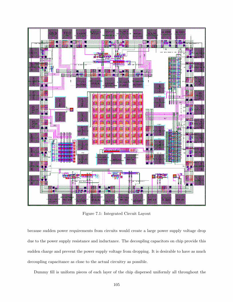
Figure 7.1: Integrated Circuit Layout
because sudden power requirements from circuits would create a large power supply voltage drop
due to the power supply resistance and inductance. The decoupling capacitors on chip provide this
sudden charge and prevent the power supply voltage from dropping. It is desirable to have as much
decoupling capacitance as close to the actual circuitry as possible.
Dummy fill is uniform pieces of each layer of the chip dispersed uniformly all throughout the
105

chip. This is usually done for polysilicon and metal layers. As these fill pieces are small compared
to the size of chip, they can be seen as a hatch pattern all throughout the chip. Dummy fill is
needed to maintain uniform density of each layer on the chip. This is essential for good planarity
in the CMP (Chemical Mechanical Polishing) step of fabrication. Figure 7.2 shows the chip layout
with decoupling capacitors and dummy fill.
Figure 7.2: IC layout with decoupling capacitors and dummy fill
106

Chapter 8
Future Improvements and Conclusion
Some suggestions for improving the designs in this thesis are described below. The thesis is sum-
marized and concluded at the end of this chapter.
8.1 Transimpedance amplifier
The transimpedance amplifier (TIA) designed for this thesis is of the shunt-shunt feedback type.
Even though functional, this topology of TIA is not suitable for interfacing with photosensors
which have a high intrinsic capacitance. This is due to the relatively high input impedance of the
TIA. Commercially available SiPMs can have capacitances in the nanoFarads owing to thousands
of APDs they contain which is needed for high dynamic range and better performance. Therefore,
the work done here can be expanded and improved by designing a TIA with the common-base
or regulated common-gate (RGC) topologies as described in [16] and [13, pp. 209–314]. These
topologies have lower input impedances that result in high bandwidth response even with highly
capacitive photosensors.
107

8.2 Comparator
The comparator design can be improved in the following ways:
1. The preamplifier can be designed using CMOS based amplifier stages so that static current
is not drawn from the DAC output. If using CMOS based amplifier compromises speed, then
only the first stage could be CMOS based and the rest could be BJT based.
2. The number of preamplifier stages could be decreased if each stage has a high enough gain.
This would reduce the preamplifier delay and reduce the setup time of the comparator.
3. The preamplifier must be designed such that its output common-mode voltage lies on the
high-gain region of the sense amplifier transconductance as discussed in Section 4.3.2.
8.3 R-2R Digital-to-Analog Converter
The R-2R DAC could be improved in the following ways:
1. A capacitance can be added on the output to reduce voltage changes due to charge injection
from the comparator input as discussed in Section 6.2.
2. The DAC input logic can be modified such that when OEN is low, the previous data is held
in another register while new serial data is being clocked into the shift register.
3. The DNL and INL characteristics of the DAC can be improved by decreasing the switch
resistance. However, a better solution is described below.
The DAC DNL and INL characteristics can also be improved by selectively increasing the
switch resistance at each bit. The DNL and INL plots in Figure 8.1 are calculated with the switch
resistances of bits shown in Table 8.1.
108

DNL
(LSB
s)
Input code
-0.025
-0.02
-0.015
-0.01
-0.005
0
0.005
0.01
0.015
0 200 400 600 800 1000 1200
INL
(LSB
s)
Input code
-0.03
-0.02
-0.01
0
0.01
0.02
0.03
0 200 400 600 800 1000 1200
Figure 8.1: DNL and INL of DAC output with switch resistances given in Table 8.1
Bit Switch resistance Slope in µV/Ω Ratio of slopes Bn+1/Bn
B9 10.00 -47.3485 –B8 20.00 -29.5928 1.600B7 38.00 -15.5362 1.905B6 68.40 -7.8606 1.994B5 116.28 -3.9419 1.999B4 186.05 -1.9724 1.999B3 279.07 -0.9864 1.999B2 390.70 -0.4932 1.999B1 507.91 -0.2466 1.999B0 609.49 -0.1233 1.999
Table 8.1: Slope of output voltage for change in switch resistance
As seen in Table 8.1, many values of switch resistances are higher than the MSB switch. The
higher switch resistances translate to smaller devices in the drive inverter. As seen in the plots,
a better performance is obtained using higher resistance switches for lower bits. Using the switch
resistance values seen in the table, there is an improvement of more than 5 times for DNL (from
-0.13 LSB to -0.025 LSB) and more than 2 times for INL (from 0.07 LSB to 0.03 LSB). Further
research is needed to find the optimal switch resistance values that could minimize the effects of
switch resistances further.
109

8.4 Conclusion
In this thesis, an analog front-end for interfacing with APDs or SiPMs was implemented. All the
components for the optical front-end - the SiPM photodetector, the APD photodetector, the TIA,
the comparator and the DAC were implemented on a monolithic chip. There is an option to use
the on-chip SiPM or an external off-chip SiPM. The TIA was analyzed for DC range, gain and
bandwidth. The comparator was analyzed for its delay and sensitivity characteristics. The DAC
was analyzed for linearity. After the components were designed and analyzed, the entire system was
assembled to test and verify the functionality. Using the components designed in this thesis to build
a discrete return LiDAR, a minimum range resolution of about 1.2 meters (3.9 ft) can be achieved.
However, range resolution value increases with increase in capacitance of the photodetector.
110
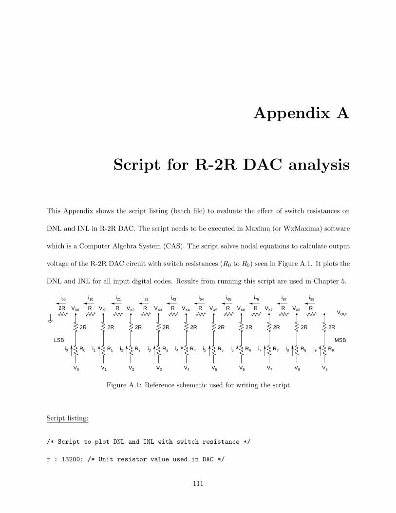
Appendix A
Script for R-2R DAC analysis
This Appendix shows the script listing (batch file) to evaluate the effect of switch resistances on
DNL and INL in R-2R DAC. The script needs to be executed in Maxima (or WxMaxima) software
which is a Computer Algebra System (CAS). The script solves nodal equations to calculate output
voltage of the R-2R DAC circuit with switch resistances (R0 to R9) seen in Figure A.1. It plots the
DNL and INL for all input digital codes. Results from running this script are used in Chapter 5.
2R
R
2R
R
2R
R
2R
R
2R
R
2R
R
2R
R
2R
R
2R
R
2R
VOUT
MSBLSB
V0 V1 V2 V3 V4 V5 V6 V7 V8 V9
2R VX0 VX1 VX2 VX3 VX4 VX5 VX6 VX7 VX8
R9R0 R1 R2 R3 R4 R5 R6 R7 R8
i00 i10 i21 i32 i43 i54 i65 i76 i87 i98
i0 i1 i2 i3 i4 i5 i6 i7 i8 i9
Figure A.1: Reference schematic used for writing the script
Script listing:
/* Script to plot DNL and INL with switch resistance */
r : 13200; /* Unit resistor value used in DAC */
111

lsb : 5/1024; /* 10-bit LSB with Vrefp = 5V and Vrefm = 0 */
/* DNL = -0.13 to 0, INL = -0.07 to 0.07 */
rsw9 : rsw8 : rsw7 : rsw6 : rsw5 : rsw4 : rsw3 : rsw2 : rsw1 : rsw0 : 10;
/* DNL = -0.025 to 0.015, INL = -0.03 to 0.03
rsw9 : 10; rsw8 : 2*rsw9; rsw7 : 1.9*rsw8; rsw6 : 1.8*rsw7; rsw5 : 1.7*rsw6;
rsw4 : 1.6*rsw5; rsw3 : 1.5*rsw4; rsw2 : 1.4*rsw3; rsw1 : 1.3*rsw2; rsw0 : 1.2*rsw1;
*/
/* Nodal equations for circuit */
i9 : ratsimp((v9 - vout)/(r9 + 2*r))$ i98 : ratsimp((vout - vx8)/r)$
vx8 : ratsimp(rhs(solve(i98 = i9,vx8)[1]))$ i98 : ratsimp((vout - vx8)/r)$
i8 : ratsimp((v8 - vx8)/(r8 + 2*r))$ i87 : ratsimp((vx8 - vx7)/r)$
vx7 : ratsimp(rhs(solve(i87 = i8 + i98,vx7)[1]))$ i87 : ratsimp((vx8 - vx7)/r)$
i7 : ratsimp((v7 - vx7)/(r7 + 2*r))$ i76 : ratsimp((vx7 - vx6)/r)$
vx6 : ratsimp(rhs(solve(i76 = i7 + i87,vx6)[1]))$ i76 : ratsimp((vx7 - vx6)/r)$
i6 : ratsimp((v6 - vx6)/(r6 + 2*r))$ i65 : ratsimp((vx6 - vx5)/r)$
vx5 : ratsimp(rhs(solve(i65 = i6 + i76,vx5)[1]))$ i65 : ratsimp((vx6 - vx5)/r)$
i5 : ratsimp((v5 - vx5)/(r5 + 2*r))$ i54 : ratsimp((vx5 - vx4)/r)$
112

vx4 : ratsimp(rhs(solve(i54 = i5 + i65,vx4)[1]))$ i54 : ratsimp((vx5 - vx4)/r)$
i4 : ratsimp((v4 - vx4)/(r4 + 2*r))$ i43 : ratsimp((vx4 - vx3)/r)$
vx3 : ratsimp(rhs(solve(i43 = i4 + i54,vx3)[1]))$ i43 : ratsimp((vx4 - vx3)/r)$
i3 : ratsimp((v3 - vx3)/(r3 + 2*r))$ i32 : ratsimp((vx3 - vx2)/r)$
vx2 : ratsimp(rhs(solve(i32 = i3 + i43,vx2)[1]))$ i32 : ratsimp((vx3 - vx2)/r)$
i2 : ratsimp((v2 - vx2)/(r2 + 2*r))$ i21 : ratsimp((vx2 - vx1)/r)$
vx1 : ratsimp(rhs(solve(i21 = i2 + i32,vx1)[1]))$ i21 : ratsimp((vx2 - vx1)/r)$
i1 : ratsimp((v1 - vx1)/(r1 + 2*r))$ i10 : ratsimp((vx1 - vx0)/r)$
vx0 : ratsimp(rhs(solve(i10 = i1 + i21,vx0)[1]))$ i10 : ratsimp((vx1 - vx0)/r)$
i0 : ratsimp((v0 - vx0)/(r0 + 2*r))$ i00 : ratsimp(vx0/(2*r))$
vout : ratsimp(rhs(solve(i00 = i0+i10,vout)[1]))$
/* allocate arrays needed */
array(voutval,1023)$ array(dnl,1022)$ array(dnl_code,1022)$
array(ref_line,1023)$ array(inl,1023)$ array(inl_code,1023)$
/* Calculate output voltage for all input codes. Each for loop for each bit */
bitnum : 0;
for bit9:0 step 5 thru 5 do block(for bit8:0 step 5 thru 5 do block(
113

for bit7:0 step 5 thru 5 do block(for bit6:0 step 5 thru 5 do block(
for bit5:0 step 5 thru 5 do block(for bit4:0 step 5 thru 5 do block(
for bit3:0 step 5 thru 5 do block(for bit2:0 step 5 thru 5 do block(
for bit1:0 step 5 thru 5 do block(for bit0:0 step 5 thru 5 do block(
voutval[bitnum] : float(subst(bit9,v9,subst(bit8,v8,subst(bit7,v7,subst(
bit6,v6,subst(bit5,v5,subst(bit4,v4,subst(bit3,v3,subst(bit2,v2,subst(
bit1,v1,subst(bit0,v0,subst(rsw0,r0,subst(rsw1,r1,subst(rsw2,r2,subst(
rsw3,r3,subst(rsw4,r4,subst(rsw5,r5,subst(rsw6,r6,subst(rsw7,r7,subst(
rsw8,r8,subst(rsw9,r9,vout))))))))))))))))))))),
bitnum : bitnum+1))))))))));
/* Calculate DNL for all codes */
for h:0 step 1 thru 1022 do block(
dnl[h] : ((voutval[h+1]-voutval[h])-lsb)/(lsb), dnl_code[h] : h);
/* Calculate gain and offset_error */
offset_error : voutval[0];
gain : (voutval[1023]-voutval[0])/1023;
/* Generate reference line for INL calculation */
for k:0 step 1 thru 1023 do ref_line[k] : (gain * k) + offset_error;
/* Calculate INL for all codes */
for q:0 step 1 thru 1023 do block(
114

inl[q] : (voutval[q] - ref_line[q])/lsb, inl_code[q] : q);
/* Plot vout, DNL and INL for all input codes */
plot2d([discrete, listarray(voutval)]);
plot2d([discrete, listarray(dnl_code), listarray(dnl)],
[xlabel, "Input code"], [ylabel, "DNL (LSBs)"]);
plot2d([discrete, listarray(inl_code), listarray(inl)],
[xlabel, "Input code"], [ylabel, "INL (LSBs)"]);
/* Calculation of slope of output voltage with respect to switch resistance */
slope_vout9 : float(at(diff(ratsimp(subst(5,v9,subst(0,v8,subst(
0,v7,subst(0,v6,subst(0,v5,subst(0,v4,subst(0,v3,subst(0,v2,subst(
0,v1,subst(0,v0,subst(0,r0,subst(0,r1,subst(0,r2,subst(0,r3,subst(
0,r4,subst(0,r5,subst(0,r6,subst(0,r7,subst(
0,r8,vout)))))))))))))))))))),r9,1),r9=0));
slope_vout8 : float(at(diff(ratsimp(subst(0,v9,subst(5,v8,subst(
0,v7,subst(0,v6,subst(0,v5,subst(0,v4,subst(0,v3,subst(0,v2,subst(
0,v1,subst(0,v0,subst(0,r0,subst(0,r1,subst(0,r2,subst(0,r3,subst(
0,r4,subst(0,r5,subst(0,r6,subst(0,r7,subst(
0,r9,vout)))))))))))))))))))),r8,1),r8=0));
slope_vout7 : float(at(diff(ratsimp(subst(0,v9,subst(0,v8,subst(
5,v7,subst(0,v6,subst(0,v5,subst(0,v4,subst(0,v3,subst(0,v2,subst(
115

0,v1,subst(0,v0,subst(0,r0,subst(0,r1,subst(0,r2,subst(0,r3,subst(
0,r4,subst(0,r5,subst(0,r6,subst(0,r8,subst(
0,r9,vout)))))))))))))))))))),r7,1),r7=0));
slope_vout6 : float(at(diff(ratsimp(subst(0,v9,subst(0,v8,subst(
0,v7,subst(5,v6,subst(0,v5,subst(0,v4,subst(0,v3,subst(0,v2,subst(
0,v1,subst(0,v0,subst(0,r0,subst(0,r1,subst(0,r2,subst(0,r3,subst(
0,r4,subst(0,r5,subst(0,r7,subst(0,r8,subst(
0,r9,vout)))))))))))))))))))),r6,1),r6=0));
slope_vout5 : float(at(diff(ratsimp(subst(0,v9,subst(0,v8,subst(
0,v7,subst(0,v6,subst(5,v5,subst(0,v4,subst(0,v3,subst(0,v2,subst(
0,v1,subst(0,v0,subst(0,r0,subst(0,r1,subst(0,r2,subst(0,r3,subst(
0,r4,subst(0,r6,subst(0,r7,subst(0,r8,subst(
0,r9,vout)))))))))))))))))))),r5,1),r5=0));
slope_vout4 : float(at(diff(ratsimp(subst(0,v9,subst(0,v8,subst(
0,v7,subst(0,v6,subst(0,v5,subst(5,v4,subst(0,v3,subst(0,v2,subst(
0,v1,subst(0,v0,subst(0,r0,subst(0,r1,subst(0,r2,subst(0,r3,subst(
0,r5,subst(0,r6,subst(0,r7,subst(0,r8,subst(
0,r9,vout)))))))))))))))))))),r4,1),r4=0));
slope_vout3 : float(at(diff(ratsimp(subst(0,v9,subst(0,v8,subst(
0,v7,subst(0,v6,subst(0,v5,subst(0,v4,subst(5,v3,subst(0,v2,subst(
116
0,v1,subst(0,v0,subst(0,r0,subst(0,r1,subst(0,r2,subst(0,r4,subst(
0,r5,subst(0,r6,subst(0,r7,subst(0,r8,subst(
0,r9,vout)))))))))))))))))))),r3,1),r3=0));
slope_vout2 : float(at(diff(ratsimp(subst(0,v9,subst(0,v8,subst(
0,v7,subst(0,v6,subst(0,v5,subst(0,v4,subst(0,v3,subst(5,v2,subst(
0,v1,subst(0,v0,subst(0,r0,subst(0,r1,subst(0,r3,subst(0,r4,subst(
0,r5,subst(0,r6,subst(0,r7,subst(0,r8,subst(
0,r9,vout)))))))))))))))))))),r2,1),r2=0));
slope_vout1 : float(at(diff(ratsimp(subst(0,v9,subst(0,v8,subst(
0,v7,subst(0,v6,subst(0,v5,subst(0,v4,subst(0,v3,subst(0,v2,subst(
5,v1,subst(0,v0,subst(0,r0,subst(0,r2,subst(0,r3,subst(0,r4,subst(
0,r5,subst(0,r6,subst(0,r7,subst(0,r8,subst(
0,r9,vout)))))))))))))))))))),r1,1),r1=0));
slope_vout0 : float(at(diff(ratsimp(subst(0,v9,subst(0,v8,subst(
0,v7,subst(0,v6,subst(0,v5,subst(0,v4,subst(0,v3,subst(0,v2,subst(
0,v1,subst(5,v0,subst(0,r1,subst(0,r2,subst(0,r3,subst(0,r4,subst(
0,r5,subst(0,r6,subst(0,r7,subst(0,r8,subst(
0,r9,vout)))))))))))))))))))),r0,1),r0=0));
/* Ratio of slopes of adjacent bits */
float(slope_vout9/slope_vout8);
117

float(slope_vout8/slope_vout7);
float(slope_vout7/slope_vout6);
float(slope_vout6/slope_vout5);
float(slope_vout5/slope_vout4);
float(slope_vout4/slope_vout3);
float(slope_vout3/slope_vout2);
float(slope_vout2/slope_vout1);
float(slope_vout1/slope_vout0);
118

Bibliography
[1] P. Eraerds, M. Legre, A. Rochas, H. Zbinden, and N. Gisin, “Sipm for fast photon-counting
and multiphoton detection,” Opt. Express, vol. 15, no. 22, pp. 14 539–14 549, Oct 2007.
[Online]. Available: http://www.opticsexpress.org/abstract.cfm?URI=oe-15-22-14539
[2] Wikipedia, “Time of flight,” Internet: https://en.wikipedia.org/wiki/Time of flight, sep. 18,
2018 [Accessed: Sep. 26, 2018].
[3] Wikipedia, “Photodiode,” Internet: https://en.wikipedia.org/wiki/Photodiode, sep. 10, 2018
[Accessed: Oct. 9, 2018].
[4] Hamamatsu, Internet: https://www.hamamatsu.com/resources/pdf/ssd/e02 handbook si
photodiode.pdf, aug. 29, 2014 [Accessed: Oct. 31, 2018].
[5] Wikipedia, “Single-photon avalanche diode,” Internet: https://en.wikipedia.org/wiki/
Single-photon avalanche diode, sep. 29, 2018 [Accessed: Oct. 2, 2018].
[6] E. A. G. Webster, L. A. Grant, and R. K. Henderson, “Transient single-photon avalanche
diode operation, minority carrier effects, and bipolar latch up,” IEEE Transactions on Electron
Devices, vol. 60, no. 3, pp. 1188–1194, March 2013.
[7] cmosedu, “Sige apds in a bicmos process,” Internet: http://cmosedu.com/jbaker/projects/
SiGe APD.htm, may. 20, 2018 [Accessed: Oct. 7, 2018].
[8] Keith Krause, “Introduction to full waveform lidar: A presentation,” Internet: https://youtu.
be/A4MWxAkolO4, sep. 2, 2016 [Accessed: Sep. 17, 2018].
[9] Keith Krause, “Nsf neon workshop: Full waveform lidar analysis,” Internet: https://bcal.
boisestate.edu/teaching/courses/NSFNEONWaveformLidarWorkshop2017, oct. 9, 2017 [Ac-
cessed: Sep. 17, 2018].
[10] T. Zhou, S. C. Popescu, K. Krause, R. D. Sheridan, and E. Putman, “Gold a novel
deconvolution algorithm with optimization for waveform lidar processing,” ISPRS Journal
of Photogrammetry and Remote Sensing, vol. 129, pp. 131 – 150, 2017. [Online]. Available:
http://www.sciencedirect.com/science/article/pii/S0924271616304968
[11] C. E. Parrish, I. Jeong, R. D. Nowak, and R. B. Smith, “Empirical comparison of full-waveform
lidar algorithms,” Photogrammetric Engineering & Remote Sensing, vol. 77, no. 8, pp. 825–838,
8 2011.
119

[12] Bob Pease, “What’s all this transimpedance amplifier stuff, any-
how? (part 1),” Internet: https://www.electronicdesign.com/analog/
whats-all-transimpedance-amplifier-stuff-anyhow-part-1, jan. 08, 2001 [Accessed: Sep.
20, 2018].
[13] R. J. Baker, CMOS Circuit Design, Layout and Simulation, 3rd ed. Wiley-IEEE Press, 2010.
[14] Sam Palermo, “Lecture 27: Transimpedance amplifiers (tias),” Internet: http://www.ece.
tamu.edu/∼spalermo/ecen474/lecture27 ee474 tias.pdf, fall, 2010 [Accessed: Sep. 17, 2018].
[15] C.-Y. Wang, C.-S. Wang, and C.-K. Wang, “An 18-mw two-stage cmos transimpedance am-
plifier for 10 gb/s optical application,” in 2007 IEEE Asian Solid-State Circuits Conference,
Nov 2007, pp. 412–415.
[16] M. d. M. Silva and L. B. Oliveira, “Regulated common-gate transimpedance amplifier designed
to operate with a silicon lt;newline/ gt;photo-multiplier at the input,” IEEE Transactions on
Circuits and Systems I: Regular Papers, vol. 61, no. 3, pp. 725–735, March 2014.
[17] A. S. Sedra and K. C. Smith, Microelectronic Circuits, 7th ed. Oxford University Press, 2014.
[18] Maxim Integrated, “Inl/dnl measurements for high-speed analog-to-digital converters (adcs),”
Internet: https://www.maximintegrated.com/en/app-notes/index.mvp/id/283, nov. 20, 2001
[Accessed: Sep. 16, 2018].
[19] Alan Wolke, “Tutorial: Digital to analog conversion – the r-2r dac,” Internet: https://www.tek.
com/blog/tutorial-digital-analog-conversion-r-2r-dac, jun. 22, 2015 [Accessed: Sep. 16, 2018].
[20] Wikipedia, “Shift register,” Internet: https://en.wikipedia.org/wiki/Shift register, mar. 23,
2018 [Accessed: Sep. 18, 2018].
[21] A. Hastings, The Art of Analog Layout, 2nd ed. Pearson, 2005.
120

Curriculum Vitae
Vikas Vinayaka
Contact:
Email: [email protected]
Education:
Bachelor of Engineering in Electronics and Communication 2010
Visvesvaraya Technological University, India
Thesis Title: Analysis and Design of Analog Front-end Circuitry for Silicon Photo-Multipliers
(SiPM) and Avalanche Photodiodes (APD) in Time-of-Flight Applications
Thesis Examination Committee:
Chairperson, Dr. R. Jacob Baker, Ph.D.
Committee Member, Dr. Biswajit Das, Ph.D.
Committee Member, Dr. Sarah Harris, Ph.D.
Graduate Faculty Representative, Dr. Zhiyong Wang, Ph.D.
121