Analogue Micropower FET Techniques Reviewepubs.surrey.ac.uk/726462/3/Analogue Micropower FET...
74
Analogue Micropower FET Techniques Review Antonio Vilches, Rodney Loga, Kostis Michelakis, Kristel Fobelets, Christos Papavasiliou, David Haigh. Optical and Semiconductor Devices Research Group. Circuits and Systems (Analogue Electronics) Research Group. Department of Electrical and Electronic Engineering, Imperial College London, Exhibition Road, London SW7 2BT. eMail: [email protected] Abstract A detailed introduction to published analogue circuit design techniques using Si and Si/SiGe FET devices for very low power applications is presented in this review. The topics discussed include subthreshold operation in FET devices, micro-current- mirrors and cascode techniques, voltage level-shifting and class-AB operation, the bulk-drive approach, the floating-gate method, micropower transconductance- capacitance and log-domain filters and strained-channel FET technologies. 1
Transcript of Analogue Micropower FET Techniques Reviewepubs.surrey.ac.uk/726462/3/Analogue Micropower FET...
Analogue Micropower FET Techniques Review
Antonio Vilches, Rodney Loga, Kostis Michelakis, Kristel Fobelets, Christos
Papavasiliou, David Haigh.
Optical and Semiconductor Devices Research Group.
Circuits and Systems (Analogue Electronics) Research Group.
Department of Electrical and Electronic Engineering,
Imperial College London, Exhibition Road, London SW7 2BT.
eMail: [email protected]
Abstract
A detailed introduction to published analogue circuit design techniques using Si and
Si/SiGe FET devices for very low power applications is presented in this review. The
topics discussed include subthreshold operation in FET devices, micro-current-
mirrors and cascode techniques, voltage level-shifting and class-AB operation, the
bulk-drive approach, the floating-gate method, micropower transconductance-
capacitance and log-domain filters and strained-channel FET technologies.
1
1. Introduction
This paper is intended to give the reader a broad overview of Si/SiGe FET device
based analogue micropower circuit design techniques and applications. The literature
survey carried out for this purpose includes work published from the late 1960’s, to
the present year, 2004. A discussion of subthreshold operation in FET devices is
followed by a detailed introduction to micro-current-mirrors and cascode techniques.
These are followed by a discussion on voltage level-shifting techniques and class-AB
operation. Reviews of the FET bulk-drive approach and floating-gate method then
precede micropower transconductance-capacitance and log-domain filters and the
paper concludes with an introduction to strained-channel FET technologies.
Micropower circuit development began in the late 1960’s due to the advent of
electronic wrist watches. Development has continued to the extent that micropower
circuits are now commonly found at the core of portable battery operated systems, in
mobile telecommunication applications, in bio/medical devices and wherever there is
a need to operate from very low voltage sources, such as those generated by
electromagnetic fields and solar radiation [1]. An excellent historical account of the
development of the field is given by Eric Vittoz, an author of many publications on
the subject, in [2].
1
In analogue design, low power operation invariably means the use of low voltage
supply because power is a function of applied voltage and drawn current [3]. The
1 The term used to define the sub-microwatt to sub-milliwatt range of operating power consumption
[1].
2
absolute limit to low power operation in analogue circuits is set by the requirement to
maintain the signal energy at a higher level than that of thermal energy, in order to
keep the signal to noise ratio, S/N, at a practical level. Hence, the minimum power
required is a function of S/N, as given by (1) [4]. In practice, it is difficult to achieve
the required S/N at micropower levels because S/N is proportional to frequency and
power [4].
NSfkTP /8min = -1
Where f is the measured signal bandwidth.
High intensity noise produced by high power drain components elsewhere on-chip,
the lack of micropower capable models and even the psychologically induced fear of
designing for operation at microampere current levels, have all contributed to hinder
the development of the field [4].
The ongoing trend in CMOS device geometry reduction may be of benefit to digital
circuits but it offers little hope to analogue designers as noise, offset requirements, as
well as an increase in output conductance, caused by short channel lengths, mean that
the successful employment of sub-micron devices in analogue micropower
applications is not a simple task [5, 6]. As a consequence, there have been a number
of techniques developed to help design low voltage applications. These include the
use of surface-channel (SC) and buried-channel (BC) FETs operating in the sub-
threshold region, micro-current-mirror pairs, self-cascode arrangements, the floating-
gate technique, use of the bulk contact to drive transistors, class-AB output stages,
current-mode filter topologies and level shifting techniques. Various combinations of
3

these techniques have been applied to solve micropower design problems and so all of
these approaches are discussed below and suitable illustrative examples are given.
Circuits involving digital switching techniques, e.g. switched capacitor and switched
current configurations , are not included as this overview is restricted to purely
analogue techniques.
2
2. Sub-Threshold Operation and Techniques
In an invertible layer FET device, the weak inversion region of operation begins when
the surface potential equals the Fermi potential, (2) [7], and strong inversion takes
place when ψ = 2ψ . s b
==
NiNa
qkTnbs lnψψ -2
Where n, (3) [8, 9], is the sub-threshold slope factor that usually lies between 1.2 and
2 for a Si MOSFET device and is inversely proportional to temperature, [5, 7, 8].
m
Bulkm
BSjOXOX
BC
gg
VCqNFS
CC
n +=+=−
+=++= 112
11 ηφγ -3
The drain current, I , in the sub-threshold region is approximated by (4) [10, 11],
which dictates that current response is exponential and proportional to temperature.
DS
2 For further information on switched micropower applications see [12,13,14,15]
4
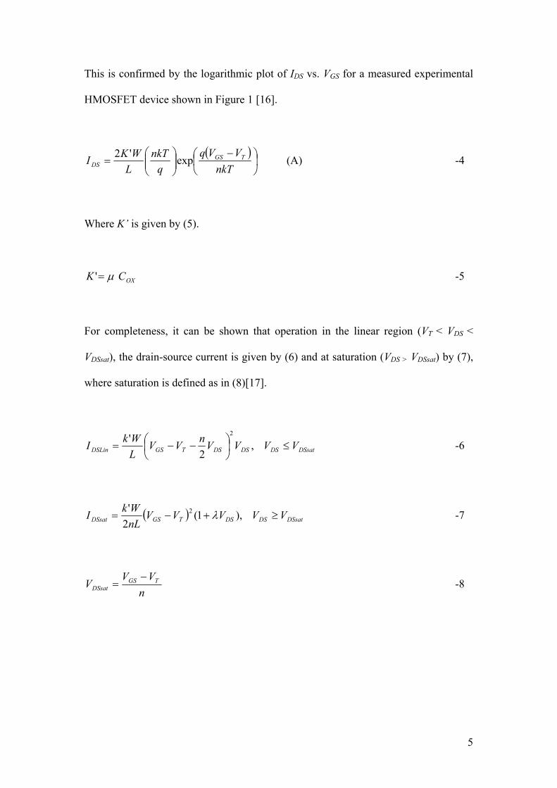
This is confirmed by the logarithmic plot of I vs. V for a measured experimental
HMOSFET device shown in Figure 1 [16].
DS GS
( )
−
=
nkTVVq
qnkT
LWKI TGS
DS exp'2 (A) -4
Where K’ is given by (5).
OXCK µ=' -5
For completeness, it can be shown that operation in the linear region (V < V <
V ), the drain-source current is given by (6) and at saturation (V V ) by (7),
where saturation is defined as in (8)[17].
T DS
DSsat DS > DSsat
DSsatDSDSDSTGSDSLin VVVVnVVLWkI ≤
−−= ,
2' 2
-6
( ) DSsatDSDSTGSDSsat VVVVVnLWkI ≥+−= ),1(
2' 2 λ -7
nVV
V TGSDSsat
−= -8
5

The main constraints to low voltage design are the device’s threshold voltage and its
inherent noise, the former being dependant on fabrication technology. It follows that
process alterations aimed at reducing turn-on voltage, V , would improve devices for
micropower use as V has a direct influence on signal-swing and dynamic range [9],
but these alterations alone cannot be relied upon because the noise margin reduces
proportionally, resulting in poor signal-to-noise ratios which complicate circuit design
considerably. Further drawbacks to be considered when designing for sub-threshold
operation are comparatively poor frequency response, the increasing effect of
substrate currents as I decreases and poor linearity [5].
T
3T
DS
On the plus side, low saturation voltages in this region (100mV to 200mV) mean that
larger voltage swings are possible for low V when compared with low V operation
for V >> V . Current response within this region, being exponential in nature, is also
similar to that of bipolar junction transistors, with the transconductance, g , being the
maximum achievable for a given value of drain current [1], even though I is
invariably low, (9) [7].
DS DS
GS T
m
DS
nkTqI
g DSm = (A/V) -9
The sub-threshold slope, S, with values ranging from 70mV to 100mV for good Si
FET devices, denotes the amount of I change per change in V in this region and is
a figure of merit often used to compare devices. The minimum value of S ensuring
weak inversion operation is approximated by (10). It has been observed that, for
DS GS
3 Defined as the range of input signals for which the active circuit will respond according to
specifications [17].
6
buried channel devices, S increases with channel depth [18] and this hinders BC
device performance with respect to SC devices.
2' T
DS
UKI
S ≥ -10
As an example of this, S = 200mV/Decade for the BC HMOSFET device measured
for Figure 1, in which the Si channel is buried at a depth of 25nm below the oxide.
However, strained BC device potential for micropower cannot be dismissed because
the strain in the BC and the removal of the carriers from the SiO interface, results in
that, for a given gate bias, the transconductance increases more rapidly than is the
case for Si MOSFETs and is always higher than in conventional FETs [19].
2
Early examples (1977) of an amplitude detector, oscillator, a band-pass filter, and a
current reference realised in MOSFET technology and designed to operate in weak
inversion with drain currents of as little as 1µA are given in [2]. A recent example of
a micropower voltage reference, employing MOSFETs in weak inversion, in which
the circuit measured response is 295mV ±10mV over a range of temperature spanning
-40°C to 130°C at a total bias of 1.2V and 100nA, is given in [20]. The principle
behind this reference circuit is that the gate-source voltage of a weakly inverted
MOSFET decreases linearly with temperature, measured at around 1mV/°K, when
biased with a constant drain current. This dependency on temperature can be negated
by extracting a current that is dependant on V and this can then be used in a negative
feedback arrangement. Such fully compensated circuits are, however, quite complex,
e.g. [20] uses 10 FET devices and 6 passive devices, 3 of which are large area
GS
7
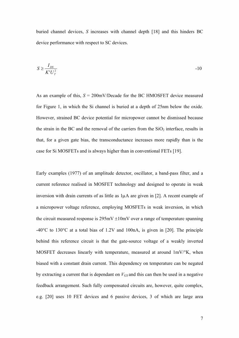
resistors. A more compact current reference Figure 2 [21], which uses a mismatch in
threshold voltages between p-MOS mirrored devices to bias one of them into
saturation whilst maintaining the other in weak inversion, is of greater potential for
use in bio-implantable applications. This uses just 4 FET devices and no passive
components, thus trading circuit size and power consumption for operating
temperature range.
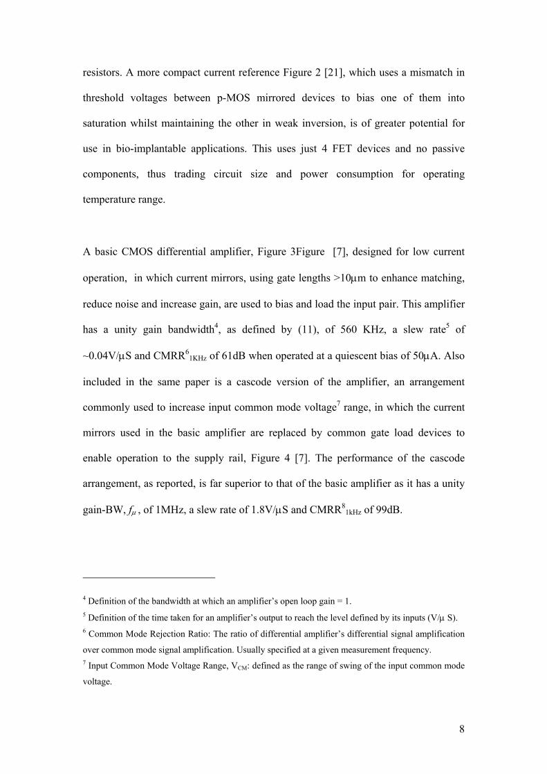
A basic CMOS differential amplifier, Figure 3 [7], designed for low current
operation, in which current mirrors, using gate lengths >10µm to enhance matching,
reduce noise and increase gain, are used to bias and load the input pair. This amplifier
has a unity gain bandwidth , as defined by (11), of 560 KHz, a slew rate of
~0.04V/µS and CMRR of 61dB when operated at a quiescent bias of 50µA. Also
included in the same paper is a cascode version of the amplifier, an arrangement
commonly used to increase input common mode voltage range, in which the current
mirrors used in the basic amplifier are replaced by common gate load devices to
enable operation to the supply rail, Figure 4 [7]. The performance of the cascode
arrangement, as reported, is far superior to that of the basic amplifier as it has a unity
gain-BW, f , of 1MHz, a slew rate of 1.8V/µS and CMRR of 99dB.
Figure
4 5
61KHz
7
8µ 1kHz
4 Definition of the bandwidth at which an amplifier’s open loop gain = 1. 5 Definition of the time taken for an amplifier’s output to reach the level defined by its inputs (V/µ S). 6 Common Mode Rejection Ratio: The ratio of differential amplifier’s differential signal amplification
over common mode signal amplification. Usually specified at a given measurement frequency. 7 Input Common Mode Voltage Range, VCM: defined as the range of swing of the input common mode
voltage.
8
C
m
Cg
fπµ 2
= (Hz) -11
Where C is the compensation capacitance used in the amplifier. C
Weak inversion MOSFETs in combination with high-Q inductors have been used in
the design of radio frequency oscillators and mixers as this combination enables the
lowest operating power for RF front-end components. Colpits voltage controlled
oscillators, VCOs, and Gilbert cell based VCOs, using this combination and operating
between 400-900MHz, with total power consumption at around 300µW are reported
in [23, 24]. Low-frequency sub-threshold operated oscillators, in which the
oscillator’s frequency is proportional to current/capacitance, have the added benefit of
a reduction in required capacitance and hence require less layout area, so that greater
miniaturisation is possible, as is essential for biomedical applications like implantable
pacemakers [24].
9
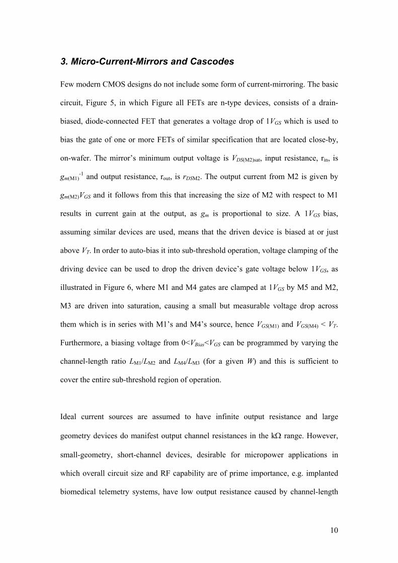
3. Micro-Current-Mirrors and Cascodes
Few modern CMOS designs do not include some form of current-mirroring. The basic
circuit, Figure 5, in which Figure all FETs are n-type devices, consists of a drain-
biased, diode-connected FET that generates a voltage drop of 1V which is used to
bias the gate of one or more FETs of similar specification that are located close-by,
on-wafer. The mirror’s minimum output voltage is V , input resistance, r , is
g and output resistance, r , is r . The output current from M2 is given by
g V and it follows from this that increasing the size of M2 with respect to M1
results in current gain at the output, as g is proportional to size. A 1V bias,
assuming similar devices are used, means that the driven device is biased at or just
above V . In order to auto-bias it into sub-threshold operation, voltage clamping of the
driving device can be used to drop the driven device’s gate voltage below 1V , as
illustrated in Figure 6, where M1 and M4 gates are clamped at 1V by M5 and M2,
M3 are driven into saturation, causing a small but measurable voltage drop across
them which is in series with M1’s and M4’s source, hence V and V < V .
Furthermore, a biasing voltage from 0<V <V can be programmed by varying the
channel-length ratio L /L and L /L (for a given W) and this is sufficient to
cover the entire sub-threshold region of operation.
GS
DS(M2)sat in
-1m(M1) DSM2out
m(M2) GS
m GS
T
GS
GS
GS(M1) GS(M4) T
Bias GS
M1 M2 M4 M3
Ideal current sources are assumed to have infinite output resistance and large
geometry devices do manifest output channel resistances in the kΩ range. However,
small-geometry, short-channel devices, desirable for micropower applications in
which overall circuit size and RF capability are of prime importance, e.g. implanted
biomedical telemetry systems, have low output resistance caused by channel-length
10
modulation9 [5] and this restricts the device’s gain. One solution to the problem is to
place two devices in series, one above the other, so that their respective channel
lengths are summed and this increases gain but also reduces output voltage swing at
the same time. A common-gate arrangement in which current input is via one of the
device’s source terminal is termed a cascode. When two devices are used with their
gates connected, the arrangement is termed a self-cascode and is equivalent to a single
composite transistor [5]. As an example, the micro-current-mirror shown in Figure 6
can be improved by the addition of a self-cascode, formed by M4 and M6, as shown
in Figure 7. Output resistance is now higher and for (W/L)M4 >> (W/L)M6, the effective
gm and β of the self-cascode stage will be those of M4. The output conductance and
minimum voltage supply required for this setup are given by (12) and (13)
respectively [25].
2
21
m
OOo g
ggg = (A/V) -12
)(2min TGS VVV −= (V) -13
9 In short channel devices, the spreading of the drain depletion region with increased bias causes the
effective channel length to be decreased.
11

Another configuration that can be used to boost output resistance is the regulated
cascode, Figure 8, where output conductance, as given by (14), is lower than for the
simple or self-cascode cases and yet the supply minimum remains the same. The
regulated cascode scheme can be extended to further decrease output conductance
whilst maintaining the same minimum supply voltage as before. An example of this
arrangement is shown in Figure 9 and the output conductance now is given by (15).
32
321
mm
OOOO gg
gggg = (A/V) -14
)12(
2
−= nm
nO
O gg
g (A/V) -15
Where n is the number of cascode stages.
If a complementary pair of devices is used to form the cascode, as given in Figure 10,
the supply can be reduced by 1VGS, thus enabling lower voltage operation. Such
arrangements are termed folded cascodes because the ac signal is anti-phase between
transistors and its path is from ground, through the M2 device and then to ground
again via M1, without going through the positive supply [26]. The configuration can
be improved with a feed-forward technique that increases BW by means of the
addition of capacitor Cp, as shown in Figure 11 [27], and this arrangement has become
the basis for a new architecture of low-voltage op-amps [27, 28]
A further benefit stemming from the use of cascode stages is a definable shift in
voltage level from input to output, a quality that is put to good use in low-voltage
design and is reviewed in section 4.
12
4. Voltage Level-Shifting and Class-AB Operation
A common problem found in low-voltage, multistage instrumentation amplifiers is
that they are not able to work with close to supply rail input common mode voltage
due to saturation in the intermediate stages. One method of solving this is to include
inter-stage voltage level-shifters as shown in Figure 12 [29], in which a precision
amplifier design, implemented in BiCMOS10 technology, is presented, that is capable
of operation with VCM close to the negative supply rail if biased with a suitable
voltage reference. The reported amplifier’s accuracy is dependant on the adequate
matching of the input voltage shifters and the stability of the shift voltage vs. input
voltage. The example given in [29] has an fµ of 500 KHz, a gain range of 5x to 2000x
and a CMRR of 90dB.
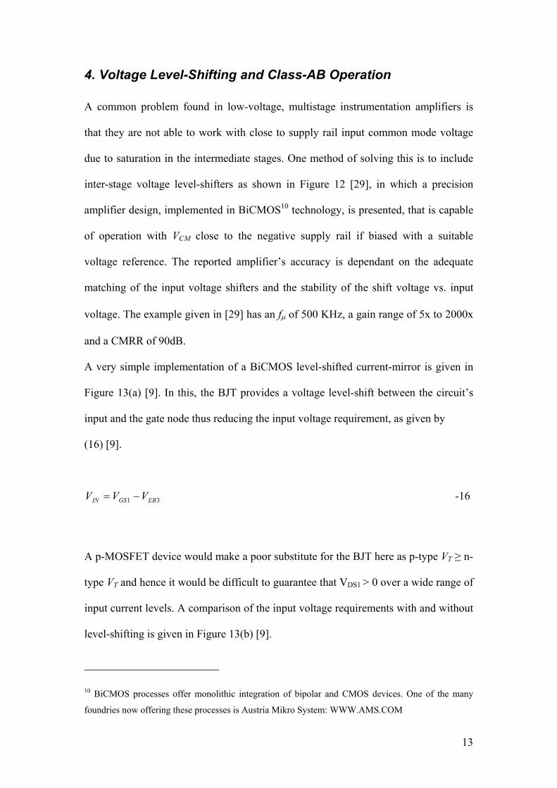
A very simple implementation of a BiCMOS level-shifted current-mirror is given in
Figure 13(a) [9]. In this, the BJT provides a voltage level-shift between the circuit’s
input and the gate node thus reducing the input voltage requirement, as given by
(16) [9].
31 EBGSIN VVV −= -16
A p-MOSFET device would make a poor substitute for the BJT here as p-type VT ≥ n-
type VT and hence it would be difficult to guarantee that VDS1 > 0 over a wide range of
input current levels. A comparison of the input voltage requirements with and without
level-shifting is given in Figure 13(b) [9].
10 BiCMOS processes offer monolithic integration of bipolar and CMOS devices. One of the many
foundries now offering these processes is Austria Mikro System: WWW.AMS.COM
13
An example of the combined use of an n-type level shifter and p-type cascode to
create an active low-voltage all-pass filter is reported in [30]. Another low-voltage
amplifier, implemented in CMOS with sub-threshold biasing, voltage level-shifting
between input and output stages by means of an intermediate current-mirror driven
cascode stage and class-AB output stages is reported in [31]. Class-AB operation is
achieved by using a control circuit to generate low impedance during the quiescent
mode of operation and hence couple the gates of the complementary output devices
together. When an input calls for one of the output transistors to deliver a large
output, the other device is kept regulated at a constant drain current while the output
devices gates are decoupled by large impedance and the control circuit routes all
incoming signal to the active device. Class-AB control circuits traditionally use a
minimum selector sub-circuit based on a decision pair of devices to control the
minimum bias current in the output stage [33]. This sub-circuit is initially
implemented in [31] by the use of an NMOS diode-coupled decision pair, Figure 14
[31]. This is termed a folded-mesh class-AB output stage and it generates a
control voltage that is sufficient to enable accurate biasing and yet is low enough to
accommodate micropower operation. A second implementation of the amplifier uses a
minimum selector that is simpler still, shown in Figure 15 [31] and a summary of
some of the measured parameters for this amplifier is given in Table 1.
11
Figure
11 All-pass filters are used to shift the phase of an analogue signal whilst keeping its amplitude
constant.
14
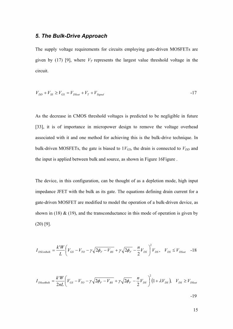
5. The Bulk-Drive Approach
The supply voltage requirements for circuits employing gate-driven MOSFETs are
given by (17) [9], where V represents the largest value threshold voltage in the
circuit.
T
SignalTDSsatGSSSDD VVVVVV ++=≥+ -17
As the decrease in CMOS threshold voltages is predicted to be negligible in future
[33], it is of importance in micropower design to remove the voltage overhead
associated with it and one method for achieving this is the bulk-drive technique. In
bulk-driven MOSFETs, the gate is biased to 1V , the drain is connected to V and
the input is applied between bulk and source, as shown in Figure 16Figure .
GS DD
The device, in this configuration, can be thought of as a depletion mode, high input
impedance JFET with the bulk as its gate. The equations defining drain current for a
gate-driven MOSFET are modified to model the operation of a bulk-driven device, as
shown in (18) & (19), and the transconductance in this mode of operation is given by
(20) [9].
DSsatDSDSDSFBSFTOGSDSLinBulk VVVVnVVVLWkI ≤
−+−−−= ,
222' 2
φγφγ -18
( ) DSsatDSDSDSFBSFTOGSDSsatBulk VVVVnVVVnLWkI ≥+
−+−−−= ,1
222
2' 2
λφγφγ
-19
15
BSF
m
BS
DSmBulk V
gVI
g−
=∆∆
=φγ
22 -20
The bulk-drive technique contributes four major benefits to low-voltage circuit design
[9]:
• Depletion mode operation leads to larger input common-mode ranges that
could not otherwise be achieved at low power supply voltages.
• The ability to totally shutoff the channel by biasing the poly gate enables a
large on/off current ratio to be achieved.
• Latch-up has not been reported to be a problem.
• Transconductance in bulk-driven mode, (20), can in theory be greater than that
obtainable with gate-drive.
On the negative side, use of the bulk as a contact means that the signal sees a larger
area than if it is injected into the gate and this results in a doubling of input
capacitance, which in turn reduces the F to around ¼ of that obtainable if gate-drive
is used (21). The device is also inherently noisier in bulk-driven mode [9].
T
TGateTBulk FF8.3η
≈ -21
Where F Gate is the transition frequency for a gate-driven device as defined by (22)
[26].
12T
12 Defined as the frequency at which current gain is 1.
16
gs
mT C
gF
π2≈ -22
As an added bonus, the bulk-to-source biasing of MOSFETs is an effective way to
reduce threshold voltage and low frequency noise, LFN, and it has been reported [3]
that Si/SiGe devices, which are V tuned in this way, do not suffer any degradation in
sub-threshold characteristics and manifest lower LFN than equivalent conventional Si
MOSFETs.
T
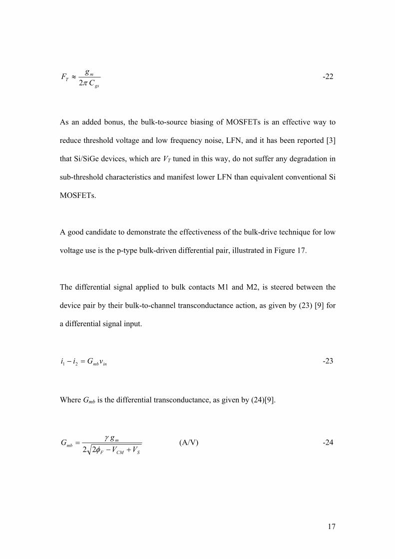
A good candidate to demonstrate the effectiveness of the bulk-drive technique for low
voltage use is the p-type bulk-driven differential pair, illustrated in Figure 17.
The differential signal applied to bulk contacts M1 and M2, is steered between the
device pair by their bulk-to-channel transconductance action, as given by (23) [9] for
a differential signal input.
inmbvGii =− 21 -23
Where G is the differential transconductance, as given by (24)[9]. mb
SCMF
mmb VV
gG
+−=
φγ
22 (A/V) -24
17
The bulk-source Si junctions cannot be forward biased within a 1V supply and hence
the pair’s input impedance is not reduced if operated within this range. This is
sustained by a reduction in threshold voltage that is proportional to the bulk-source
junction’s applied forward-bias, so that the source voltage follows V linearly to a
certain extent with measurements confirming that input currents are of the order of
nA, even at the extreme ranges of V input (e.g. at +0.5V for Si) [9]. However, as
mentioned previously, the input capacitance per device is greater than what would be
present for a gate-driven differential pair and hence, although the output capacitance
CM
CM
and hence the frequency pole of both types remain similar, the bulk-driven
arrangement has a lower gain-BW product than its gate-driven counterpart [9].
Another good example of the use of bulk-drive for low voltage design is the cascode
bulk-driven MOSFET current mirror shown in Figure 18 [9]. This arrangement is
capable of operation at 1V V whereas its gate-driven counterpart is not. The
circuit’s main advantages are the very low voltage required at the input of the current
mirrors, the extremely low input currents required, good input and output current
matching and a reasonable output conductance due to the cascode stage. The main
drawback is a lack of BW when compared with a gate-driven arrangement.
DD
Bulk-drive is also used to increase input common mode range in the low-power
CMOS op-amp reported in [34]. Designed to operate from a 1V supply, it has an open
loop gain of 70dB and a gain-BW product of 190kHz at 5µW power drain.
As a final example of the use of bulk-drive in low voltage design, Blalock et al in [9]
present a BiCMOS op-amp realisation that uses a bulk-driven differential pair, a
simple current mirror with voltage level shifting (as described in section 4) and simple
18
class-A output stage. In this, the simple current-mirror with p-type BJT level shifter is
chosen as it is preferred over a bulk-driven arrangement for its greater bandwidth and
comparable low input voltage requirements. The authors, although acknowledging
that class-AB is the preferred output stage arrangement, do not use a class-AB stage
because of limited BW at 1V, in the case of a bulk-driven current-mirror or simple
pMOS gate-driven current-mirror, and a limited output impedance in the case of a
current-mirror using lateral BJT’s which are commonly available in standard CMOS
processes. The amplifier, shown in Figure 19 [9], is implemented in 2µm gate-length
technology, has a total quiescent power dissipation of 300µW at a tail current of
100µA, a DC gain of 48.8dB at a mid-supply V and a unity-gain frequency of
1.3MHz.
CM
6. The Floating-Gate Method
The first floating-gate structure was originally reported in 1967 as a mechanism for
non-volatile information storage [35, 36]. Research into the field has grown steadily
as it offers promising solutions to present and future integrated circuit solutions
because the physical effects of hot-electron injection and electron tunnelling (see
below) become more pronounced as CMOS process geometries are scaled down [36].
In the floating-gate method, insulated gate devices13 can be driven by any one of three
mechanisms:
a. By raising electron energy through exposure to UV light.
b. By Fowler-Nordheim Tunnelling.
c. By hot-electron injection.
13 Floating-gate devices are MOSFETs with an added insulating oxide layer on-top of the gate metal.
19
Fowler-Nordheim Tunnelling and hot-electron injection can be used to dynamically
adjust the gate-charge and hence are the mechanisms of choice [37]. Both
mechanisms are explained below.
6.1 Hot-Electron Injection
The intense electric fields produced by MOSFET devices operated in weak-inversion
cause electrons near the surface of a semiconductor to acquire sufficient energy to
overcome the Si/SiO barrier and enter the Si conduction band. Once there, the
applied electric field sweeps the carriers across to the floating-gate. As increased V
favours hot-electron injection, floating-gate transistors are engineered to have higher
than usual threshold voltages. This is achieved by increasing substrate doping levels
(e.g. by placing a highly doped PTUB directly on a p-type substrate and fabricating an
NMOS device within). The injected current is given by (25).
2
T
= inj
DC
VV
Sinj eII β -25
Where V and β are fit constants [37]. inj
6.2 Fowler-Nordheim Tunnelling
Originally described in [38], Fowler-Nordheim electron tunnelling is possible because
the wave nature of electrons grants them a finite probability of passing what was
originally believed to be an impassable oxide barrier. The probability of overcoming
the barrier and hence the effective current produced is increased by increasing the
20
electric field strength across the barrier. The expression for the tunnelling current is
given in (26) [37]. One drawback of this approach is that continued carrier injection
and tunnelling will eventually degrade the oxide quality and hence the tunnelling
voltage and floating-gate drain current have to be kept low to minimise this [37].
fgtun
oox
VVt
tun eII −=ε
0 -26
Where V is the tunnelling voltage and V is the floating-gate voltage. tun fg
The gates on floating-gate devices are usually coupled to incoming signals by
capacitors, as shown in Figure 20Figure which represents a typical arrangement.
Capacitive coupling blocks the transfer of DC current and hence enables the device’s
gate to ‘float’ at the voltage dictated by the input capacitances, which are termed
control gates.
The voltage on the gate is the weighted sum of both input voltages, one of which is
the signal and the other is used for biasing, as given by (27).
212
2121
211
CCQV
CCCV
CCCV fg +
++
++
= -27
Charge Q offsets the threshold voltage and can be dynamically modified as previously
explained. The result is that the inputs couple into the floating-gate down to close to
DC (mHz range) [39].
21
The handling of offset mismatches within floating-gate amplifiers has been of major
concern to researchers. Various clocking-based schemes have been reported [40, 41,
42, 43] in which the offset voltage is periodically calculated and subtracted during a
set time-period and these result in almost continuous operation, at the expense of
extra, complicated circuitry. Recently, the concept of auto-input offset removal using
feedback via the tunnelling and hot-electron mechanisms previously discussed has
been introduced in [37], in which a floating-gate pseudo-differential transconductor is
simulated using this technique.
The floating-gate method lends itself well to the design of micropower amplifiers as
the input common mode range is increased due to the attenuation of the input signal
by a factor of C1/(C1+C2+Cparasitics). However, this attenuation forces trade-offs to
be made between V and gain as well between gain-BW and noise [44]. CM
An example of a micropower CMOS op-amp, using floating-gate input transistors, is
shown in Figure 21Figure . The amplifier is intended for operation in the kHz range,
operates from a single 1.2V supply and consumes just 4.3µA. Measured DC gain is
65dB, gain-BW is 230kHz and slew-rate is 184mV/µS [44].
A multiple input operational amplifier based on floating-gate devices is described in
[45], Figure 22Figure , in which the circuit, featuring three differential inputs, is
biased to 40µA. Measured unity gain-BW is 360kHz, with a slew-rate of 2V/µS,
which although impressive for a micropower amplifier, is offset by the fact that dual
5V supplies are used. The FET resistor and 20pF capacitance on the RHS of the figure
are for frequency compensation.
22
A micropower second-order band/low pass log-domain filter using floating-gate
devices operating in weak inversion, has also been reported recently [46]. The circuit
features a 1V supply rail, a 2µW power-drain and uses less than 1µW per pole.
14
Another salient feature of floating-gate systems is that it is possible to design so that
they adapt to incoming and outgoing signals, whilst preserving the resulting network
state when set. This property resulted in the development of single transistor synapses,
in which single floating-gate FETs are used to emulate the computational and
adaptive properties of biological synaptic elements [47] and has recently resulted in
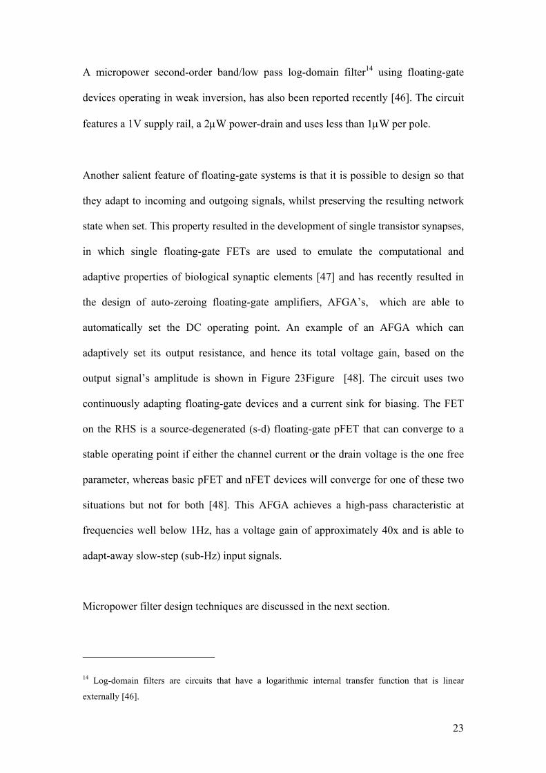
the design of auto-zeroing floating-gate amplifiers, AFGA’s, which are able to
automatically set the DC operating point. An example of an AFGA which can
adaptively set its output resistance, and hence its total voltage gain, based on the
output signal’s amplitude is shown in Figure 23 [48]. The circuit uses two
continuously adapting floating-gate devices and a current sink for biasing. The FET
on the RHS is a source-degenerated (s-d) floating-gate pFET that can converge to a
stable operating point if either the channel current or the drain voltage is the one free
parameter, whereas basic pFET and nFET devices will converge for one of these two
situations but not for both [48]. This AFGA achieves a high-pass characteristic at
frequencies well below 1Hz, has a voltage gain of approximately 40x and is able to
adapt-away slow-step (sub-Hz) input signals.
Figure
Micropower filter design techniques are discussed in the next section.
14 Log-domain filters are circuits that have a logarithmic internal transfer function that is linear
externally [46].
23
7. Filtering at Micropower
Filter functions can obviously be implemented using many techniques. All are not
mentioned here as a full review of all the relevant filter theory is beyond the bounds
of this general micropower review. The existing range of true micropower filter
solutions can be broadly divided into two popular types:
-Transconductance-capacitance (GM-C) Filters.
- Log-domain Filters.
A brief description of each type with reference to any micropower techniques used in
their implementation is given below.
7.1 GM-C Filters
Transconductance-capacitance filters rely on transconductors to charge/discharge an
integrating capacitance and hence obtain the required frequency response. The
transconductor converts the input voltage into a proportional amount of current and
the integrating capacitance, integrates and converts this back into voltage form. Hence
capacitor current in these filters is a linear function of input voltage. These are quite
popular for high-frequency filter applications because the transconductors tend to
have a higher BW than op-amps, can be tuned electronically and are easily
implemented monolithically [49]. They can be constructed using voltage-mode (input
signals are voltages) or current-mode (input signals are currents) approaches but it has
been concluded that voltage-mode implementations offer the best performance [49].
24
As examples of these arrangements, a voltage-mode single-pole schematic of a GM-C
filter is shown in Figure 24 (a) and Figure 24(b) shows a second order
configuration, commonly referred to as a bi-quad.
Figure
Although normally designed with FET devices biased into saturation, there have been
attempts to reduce power consumption and voltage supply constraints by operating
the transconductor/s in weak inversion because it is known that sub-threshold versions
of these filters are well suited for bionic cochlear implants, as they are able to tune
over the entire frequency spectrum of hearing at reduced power consumption [50].
An example of this approach is given in [52] where a differential transconductor
employing sub-threshold biased MOSFETs is used to ensure micropower operation.
Special attention is paid to the biasing of these transistors as current mismatches in the
differential branches can lead to DC signals that can cause a large variation of the
operating point at the output and so a complicated common mode feedback control
circuit is added to source/sink the difference in the current required to maintain the
circuit stable. The second order filter achieves stable, programmable operation at
290nW (10nA bias current) at the expense of a comparatively large footprint
(200µmx300µm without adding the area of the integrating capacitor). An earlier, third
order GM-C filter featuring a 1.5V supply and total power consumption of 138µW is
presented in [52]. This also uses a differential input and common mode feedback to
ensure adequate bias and improve the differential-input swing.
25
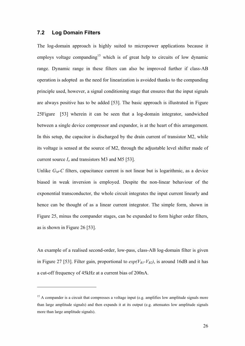
7.2 Log Domain Filters
The log-domain approach is highly suited to micropower applications because it
employs voltage companding15 which is of great help to circuits of low dynamic
range. Dynamic range in these filters can also be improved further if class-AB
operation is adopted as the need for linearization is avoided thanks to the companding
principle used, however, a signal conditioning stage that ensures that the input signals
are always positive has to be added [53]. The basic approach is illustrated in Figure
25Figure [53] wherein it can be seen that a log-domain integrator, sandwiched
between a single device compressor and expandor, is at the heart of this arrangement.
In this setup, the capacitor is discharged by the drain current of transistor M2, while
its voltage is sensed at the source of M2, through the adjustable level shifter made of
current source Io and transistors M3 and M5 [53].
Unlike GM-C filters, capacitance current is not linear but is logarithmic, as a device
biased in weak inversion is employed. Despite the non-linear behaviour of the
exponential transconductor, the whole circuit integrates the input current linearly and
hence can be thought of as a linear current integrator. The simple form, shown in
Figure 25, minus the compander stages, can be expanded to form higher order filters,
as is shown in Figure 26 [53].
An example of a realised second-order, low-pass, class-AB log-domain filter is given
in Figure 27 [53]. Filter gain, proportional to exp(VB1-VB2), is around 16dB and it has
a cut-off frequency of 45kHz at a current bias of 200nA.
15 A compander is a circuit that compresses a voltage input (e.g. amplifies low amplitude signals more
than large amplitude signals) and then expands it at its output (e.g. attenuates low amplitude signals
more than large amplitude signals).
26
As with GM-C filters, operating point stability is also an issue here and techniques
have been developed to ensure that all the filter devices remain in weak inversion.
One technique, given in [54], uses a voltage comparator to control a FET connected to
the monitored node and thus apply the necessary negative feedback required to
stabilise the operating point.
Log-domain filters, invariably, find use in micropower biomedical applications [55,
56], a good example of which is given in [57], in which this type of filter is at the
heart of a mixed-signal cochlear implant. The implantable system features a flat
voltage gain of around 30x, a BW of 200Hz and total power consumption of 126µW.
8. Buried-Channel FET Technologies
Work on SiGe/Si hetero-junction FET devices began in the early eighties with a view
to exploiting their comparatively higher mobilities, resulting from the use of a
strained channel, in order to increase the speed of pMOS devices whilst retaining
compatibility with CMOS fabrication technology [58, 59]. HFETs were originally
fabricated in GaAs using Schottky gate contacts and implanted, near surface channels
[60]. The need for integration with CMOS technology together with advances in SiGe
processing, including the use of molecular beam epitaxy to grow the hetero-junction
directly and with greater precision, resulted in improved device performance [62].The
concept was extended by the addition of a gate-oxide as a barrier to prevent high
leakage currents via the gate contact [62] and by the growth of MBE layers on relaxed
SiGe buffer layers (termed a virtual substrate), an innovation that offers the possibility
to grow thin (~8nm) strained Si channels in SiGe. N-type HMOSFET devices grown
by fabricating the active n-type layers on relaxed p-type SiGe buffer layers, were
27
presented originally in [63, 64] and more recently in [65, 66, 67, 68, 16, 69, 19, 70,
71]. Burying the channel (strained or unstrained) further from the gate was reported to
reduce surface carrier trapping, caused by the high density of interface states at the
oxide/SiGe interface, and increase the mobility of the channel-confined carriers at the
expense of a decrease in transconductance due to the channel’s greater distance from
the applied gate voltage [72, 73, 74]. It was clear that in strained BC devices the
transconductance gm, for a given gate-bias, increases more rapidly than is the case for
Si MOSFETs and this is due to a lower sub-threshold slope at low to high VT and is
always higher than in conventional FETs. Hence, it was concluded that the extra boost
in gm at low bias levels warrants the use of these devices in micropower applications
where battery life is of prime importance and / or overall heat dissipation are an issue
[19, 75, 76].
Continuing the trend in development, there has been a comparatively recent move to
Si/SiGe on Insulator technologies, Si/SiGe/SOI, in an attempt to further improve both
the micropower capability and BW of HFET devices. SOI technologies make use of a
thick oxide layer between the substrate and active layers in order to minimise active-
layer-to-substrate currents and substrate parasitic capacitances. These technologies are
reported to be quasi-ideal for micropower and RF circuit functionalities as well as for
high-temperature operation up to about 350°C.[77, 78, 79, 80, 81, 82].
9. Concluding Remarks
This review presented has shown that there is an ongoing effort to produce new FET
technologies in order to improve on bulk device performance at low power. HFETs
are seen as a good candidate for this as results confirm that mobility and hence
28
transconductance is greater than what is reported for similar geometry MOSFETs.
The review has also shown that there are a number of tried and tested methodologies
used in the design of low voltage / micropower FET circuitry. Some approaches like
sub-threshold operation, floating-gate and bulk-drive methods can be considered
device related whilst others, like the use of micro-current mirrors, self-cascode
arrangements, voltage level-shifting and class-AB output stages, are clearly circuit
based techniques. Although presently micropower design is targeted almost
exclusively at Si CMOS technologies, the advent of strained surface and buried
channel FETs in Si/SiGe and SOI is sure to revolutionise the field as the micropower
benefits of these devices over the traditional MOSFET become accepted.
29
References
1. Vittoz, E.A.; “Very Low Power Circuit Design: Fundamentals And Limits”.
Circuits and Systems, 1993., ISCAS '93, 1993 IEEE International Symposium on , 3-6
May 1993, Page(s): 1439 -1442
2. Vittoz, E.; Fellrath, J.; “CMOS analog integrated circuits based on weak inversion
operations”. Solid-State Circuits, IEEE Journal of , Volume: 12 Issue: 3 , Jun 1977,
Page(s): 224 -231
3. Pei-Wen Li; Wei-Ming Liao; Ching-Chieh Shih; Tine-Shang Kuo; Li-Shyue Lai;
Yang-Tai Tseng; Tsai, M.-J.; “Effect of substrate biasing on Si/SiGe heterostructure
MOSFETs for low-power circuit applications”. Electron Device Letters, IEEE,
Volume: 24 Issue: 7 , July 2003 Page(s): 454 -456
4. Vittoz, E.A.; “Low-power design: ways to approach the limits”. .Solid-State
Circuits Conference, 1994. Digest of Technical Papers. 41st ISSCC., 1994 IEEE
International , 16-18 Feb. 1994, Page(s): 14 -18
5. Rajput, S.S.; Jamuar, S.S., “Low voltage analog circuit design techniques Circuits
and Systems Magazine”, IEEE , Volume: 2 Issue: 1 , 2002 Page(s): 24 -42.
6. De Langen, K.-J.; Huijsing, J.H., “Compact low-voltage power-efficient
operational amplifier cells for VLSI”. Solid-State Circuits, IEEE Journal of, Volume:
33 Issue: 10 , Oct. 1998 Page(s): 1482 -1496.
30
7. Stone, D.C.; Schroeder, J.E.; Smith, A.R.; “Analog CMOS Building Blocks for
Custom and Semicustom Applications”. Solid-State Circuits, IEEE Journal of,
Volume: 19 Issue: 1 , Feb 1984 Page(s): 55 -61
8. Vittoz, E.; Fellrath, J.; “CMOS analog integrated circuits based on weak inversion
operations”. Solid-State Circuits, IEEE Journal of , Volume: 12 Issue: 3 , Jun 1977,
Page(s): 224 -231
9. Blalock, B.J.; Allen, P.E.; Rincon-Mora, G.A.; “Designing 1-V op amps using
standard digital CMOS technology”. Circuits and Systems II: Analog and Digital
Signal Processing, IEEE Transactions on , Volume: 45 Issue: 7 , July 1998 , Page(s):
769 -780
10. C.T.Shah, “Characterization of the Metal Oxide Semiconductor Transistors”.
IEEE Trans. Electron Devices, ED-11, pp.324-345, July 1964.
11. R.L.Geiger, P.E. Allen and N.R.Strader, “VLSI Design Techniques for Analog
and Digital Circuits”. New York, McGraw Hill, 1990.
12. Hughes, J.B.; Worapishet, A.; Toumazou, C.; “Switched-capacitors versus
switched-currents: a theoretical comparison [in CMOS]”. Circuits and Systems, 2000.
Proceedings. ISCAS 2000 Geneva. The 2000 IEEE International Symposium on ,
Volume: 2 , 28-31 May 2000, Page(s): 409 -412 vol.2
31
13. Leelavattananon, K.; Toumazou, C.; Hughes, J.B.; “Linearity enhancement
techniques for MOSFET-only SC circuits”. Circuits and Systems, 2000. Proceedings.
ISCAS 2000 Geneva. The 2000 IEEE International Symposium on , Volume: 5 , 28-
31 May 2000, Page(s): 453 -456 vol.5
14. Bazarjani, S.S.; Snelgrove, W.M.; “Low voltage SC circuit design with low -Vt
MOSFETs”. Circuits and Systems, 1995. ISCAS '95., 1995 IEEE International
Symposium on , Volume: 2 , 28 April-3 May 1995, Page(s): 1021 -1024 vol.2
15. Degrauwe, M.; Vittoz, E.; Verbauwhede, I.; “A Micropower CMOS-
Instrumentation Amplifier”. Solid-State Circuits, IEEE Journal of , Volume: 20 Issue:
3 , Jun 1985, Page(s): 805 -807
16. K. Michelakis, S. Despotopoulos, V. Gaspari, A. Vilches, K. Fobelets, C.
Papavassiliou, C. Toumazou, J. Zhang, “SiGe virtual substrate HMOS transistor for
analogue applications”. First International SiGe Technology and Device Meeting
(ISTDM 2003), Jan. 2003. Also accepted for publication in a regular issue of Applied
Surface Science.
17. K.Laker and W.Sansen.; “Design of Analogue Integrated Circuits and Systems”.
NewYork: McGraw Hill, 1994, pp20--22.
18. Montree, A.H.; Meijssen, V.M.H.; Woerlee, P.H., “Comparison of buried and
surface channel PMOS devices for low voltage 0.5 µm CMOS”. VLSI Technology,
32
Systems, and Applications, 1993. Proceedings of Technical Papers. 1993 International
Symposium on , 12-14 May 1993 Page(s): 11 -14
19. Papavassiliou C., Fobelets K., Toumazou C. "SiGe hetero-FET potential for
micro-power applications" invited paper, IEICE Trans. Electron, E00-A(2000)
20. Giustolisi, G., Criscione, M., Cutri, F.; "A Low-Voltage Low-Power Voltage
Reference Based on Subthreshold MOSFETs". IEEE J. Solid State Circuits, Vol.38,
N.1,pp.151-154, Jan. 2003.
21. Georgiou, J.; Toumazou, C.; “A resistorless low current reference circuit for
implantable devices”. Circuits and Systems, 2002. ISCAS 2002. IEEE International
Symposium on , Volume: 3 , 26-29 May 2002, Page(s): III-193 -III-196 vol.3
22. Lin, T.H., Sanchez, H., Rofougaran, R. and Kaiser, W.J.; "Micropower CMOS RF
Components for Distributed Wireless Sensors". Radio Frequency Integrated Circuits
(RFIC) Symposium, 1998 IEEE , 7-9 June 1998 Page(s): 157 -160
23. "Rofougaran, R., Lin, T.H., Kaiser, W.J..; "CMOS Front-Edn LNA Mixer for
Micropower RF Wireless Systems". Low Power Electronics and Design, 1999.
Proceedings. 1999 International Symposium on , 16-17 Aug. 1999
Page(s): 238 -242
33

24. Hwang, C., Bibyk, S., Ismail, M., Lohiser, B.; "A Very Low Frequency,
Micropower, Low Voltage CMOS Oscillator for Noncardiac Pacemakers". IEEE J.
Trans. Circuits and Systems, Chap.1, Vol.42, N.11, pp.962-966, Nov. 1995.
25. Toumazou, C., Burdett, A., Lidgey, J.; “High Frequency CMOS and Bipolar
Analog IC Design”. Continuing Professional Development course, Imperial College
London, April 2002.
26. Laker. K.R, Samsen, W.M.C.; "Design of analog integrated circuits and systems".
McGraw Hill, ISBN 0-07-113458-1
27. Setty, S.; Toumazou, C.; “A new architecture for low voltage CMOS operational
amplifiers”. Circuits and Systems, 1997. ISCAS '97, Proceedings of 1997 IEEE
International Symposium on , Volume: 1 , 9-12 June 1997, Page(s): 225 -228 vol.1
28. Setty, S.; Toumazou, C.; “Feedforward compensation techniques in the design of
low voltage opamps and OTAs”. Circuits and Systems, 1998. ISCAS '98. Proceedings
of the 1998 IEEE International Symposium on , Volume: 1 , 31 May-3 June 1998,
Page(s): 464 -467 vol.1
29. Ivanov, V. V.; “A micropower Precision Single-Supply Instrumentation
Amplifier”. ISSCC, Section 21, 1997.
34
30. T.P.Pearsall, J.C.Bean, "Enhancement and depletion mode p-channel GexSii-x
modulation doped FETs." IEEE Electron Device Lett., vol. EDL-7, pp. 308-310,
1986.
31. De Langen, K.-J.; Huijsing, J.H., “Compact low-voltage power-efficient
operational amplifier cells for VLSI”. Solid-State Circuits, IEEE Journal of, Volume:
33 Issue: 10 , Oct. 1998 Page(s): 1482 -1496.
32. E.Seevinck, W. de Jager and P.Buitendijk, "A low-distortion output stage with
improved stability for monolithic power amplfiers". IEEE J. Solid-State Circuits,
vol.23, pp794-801, Dec. 1986.
33. C.Hu.; “Future CMOS scaling and reliability”. Proc. IEEE, Vol. 81, pp682-652,
May 1993.
34. Lasanen, K.; Raisanen-Ruotsalainen, E.; Kostamovaara, J.; “A 1-V 5 µW CMOS-
opamp with bulk-driven input transistors”. Circuits and Systems, 2000. Proceedings
of the 43rd IEEE Midwest Symposium on , Volume: 3 , 8-11 Aug. 2000 Page(s):
1038 -1041.
35. Hasler, P.; Minch, B.A.; Diorio, C.; “Floating-gate devices: they are not just for
digital memories any more”. Circuits and Systems, 1999. ISCAS '99. Proceedings of
the 1999 IEEE International Symposium on , Volume: 2 , 30 May-2 June 1999,
Page(s): 388 -391 vol.2
35
36. Kahng,D. and Sze, S.M.; "A floating gate and its application to memory devices".
The Bell System Technical Journal, Vol. 46, n.4, 1967, pp. 1288-1295.
37. Constandinou, T.G.; Georgiou, J.; Toumazou, C.; “An auto-input-offset removing
floating gate pseudo-differential transconductor”. Circuits and Systems, 2003. ISCAS
'03. Proceedings of the 2003 International Symposium on , Volume: 1 , May 25-28,
2003, Page(s): 169 -172
38. Lenzinger, M. and Snow, E.H.; "Fowler-Nordheim Tunnelling into Thermally
grown SiO2". J. Applied Phys., Vol.40, pp.278-282, 1969.
39. Minch, B.A.;"Low-Voltage Topologies for Analog and Mixed-SIgnal Circuits in
Nanoscale CMOS". Mixed Analog-Digital VLSI Circuits & Systems Laboratory.
CORNELL U N I V E R S I T Y School of Electrical and omputer Engineering.
40. Yu, C.-G.; Geiger, R.L.; “Very low voltage operational amplifiers using floating
gate MOS transistor”. Circuits and Systems, 1993., ISCAS '93, 1993 IEEE
International Symposium on , 3-6 May 1993, Page(s): 1152 -1155 vol.2
41. Carley, L.R.; “Trimming analog circuits using floating-gate analog MOS
memory”. Solid-State Circuits Conference, 1989. Digest of Technical Papers. 36th
ISSCC., 1989 IEEE International , 15-17 Feb. 1989, Page(s): 202 -203
36
42. Hasler, P.; Minch, B.A.; Diorio, C.; “Adaptive circuits using pFET floating-gate
devices”. Advanced Research in VLSI, 1999. Proceedings. 20th Anniversary
Conference on , 21-24 March 1999, Page(s): 215 -229
43. Vincent, F.K., Goodman, R.; "Dynamic Charge Restoration of Floating Gate
Subthreshold MOS Translinear Circuits". IEEE, 2001.
44. Raisanen-Ruotsalainen, E.; Lasanen, K.; Kostamovaara, J.; “A 1.2 V micropower
CMOS op amp with floating-gate input transistors”. Circuits and Systems, 2000.
Proceedings of the 43rd IEEE Midwest Symposium on , Volume: 2 , 8-11 Aug. 2000,
Page(s): 794 -797 vol.2
45. Kewei Yang; Andreou, A.G.; “Multiple input floating-gate MOS differential
amplifiers and applications for analog computation”. Circuits and Systems, 1993.,
Proceedings of the 36th Midwest Symposium on , 16-18 Aug. 1993, Page(s): 1212 -
1216 vol.
46. Rodriguez-Villegas, E.O.; Rueda, A.; Yufera, A.; “A micropower log domain
FGMOS filter”. Circuits and Systems, 2002. ISCAS 2002. IEEE International
Symposium on , Volume: 3 , 26-29 May 2002, Page(s): III-317 -III-320 vol.3
47. Hasler, P., Dorio, C., Minch, B.A. and Mead, C.; "Single Transistor Learning
Synapses". Advances in Neural Information Processing Systems 7, MIT Press,
Cambridge, MA, 1995, pp. 817-824.
37
48. Hasler, P.; Smith, P.D.; “An autozeroing floating-gate amplifier with gain
adaptation”. Circuits and Systems, 1999. ISCAS '99. Proceedings of the 1999 IEEE
International Symposium on , Volume: 2 , 30 May-2 June 1999, Page(s): 412 -415
vol.2
49. Mahattanakul, J., Toumazou, C.; "Current-Mode Versus Voltage Mode GM-C
Biquad Filters: What the Theory Says". IEEE Trans. Circuits and Systems II, Vol.45,
N.2, pp173-186, Feb.1998.
50. Lu, T.K.-T.; Baker, M.; Salthouse, C.D.; Ji-Jon Si; Zhak, S.; Sarpeshkar, R.; “A
micropower analog VLSI processing channel for bionic ears and speech-recognition
front ends”. Circuits and Systems, 2003. ISCAS '03. Proceedings of the 2003
International Symposium on , Volume: 5 , May 25-28, 2003 Page(s): 41 -44
51. Rodriguez-Villegas, E.; Payne, A.J.; Toumazou, C.; “A 290 nW, weak inversion,
Gm-C biquad”. Circuits and Systems, 2002. ISCAS 2002. IEEE International
Symposium on , Volume: 2 , 26-29 May 2002, Page(s): II-221 -II-224 vol.2
52. Chi-Hung Lin, Ismail, M.; "A 1.5V 3rd-order Fully Differential CMOS GM-C
Filter and Micropower Class-AB V-I Converters”. ICN'98, pp.208-210, December
1998.
53. Python, D., Enz, C.C.; "A micropower Class-AB CMOS Log-Domain Filter for
DECT Applications". IEEE J. Solid State Circuits, Vol.36, N.7, July 2001.
38
54. Georgiou, J.; Toumazou, C.; “An operating point elimination technique for weak-
inversion log-domain filters with multiple operating points”. Circuits and Systems,
2001. ISCAS 2001. The 2001 IEEE International Symposium on , Volume: 1 , 6-9
May 2001, Page(s): 153 -155 vol. 1
55. Georgiou, J.; Drakakis, E.M.; Toumazou, C.; Premanoj, P.; “An analogue
micropower log-domain silicon circuit for the Hodgkin and Huxley nerve axon”.
Circuits and Systems, 1999. ISCAS '99. Proceedings of the 1999 IEEE International
Symposium on , Volume: 2 , 30 May-2 June 1999, Page(s): 286 -289 vol.2
56. Germanovix, V., O'Neil, G., Toumazou, C., Drakakis, E.M., Kitney, R.I., Lande,
T.S.; "Analogue micropowered log-domain tone controller for auditory prostheses".
IEE Electronic Letters, Vol.34, N.11, 28th May 1998.
57. Georgiou, J.; Toumazou, C.; “A micropower cochlear prosthesis system”. Circuits
and Systems, 2003. ISCAS '03. Proceedings of the 2003 International Symposium on
, Volume: 3 , May 25-28, 2003, Page(s): 834 -837
58. Toker, A.; Ozoguz, S.; “Tunable allpass filter for low voltage operation”.
Electronics Letters , Volume: 39 Issue: 2 , 23 Jan. 2003, Page(s): 175 -176
59. O’Neill, A. G., and Antoniadis, D. A.: “Investigation of Si/SiGe-Based FET
Geometries for High Frequency Performance by Computer Simulation”, IEEE Trans.
Electron Devices, Jan. 1997, Vol. 44, pp. 80-88
39
60. R.Williams; "Modern GaAs Processing Methods". Artech House, Boston,
London. 1990, pp354. ISBN: 0-89006-343-5
61. Gluck, M., Hackbarth, T., König, U., Haas, A., Hock, G., Kohn, E.: “High fmax
n-type Si/SiGe MODFETs”. Electronics Letters, Volume: 33 Issue: 4 , 3 Feb 1997
Page(s): 335 –337.
62. D.Nayak, J.C.S.Woo, J.S.Park, K.L.Wang and K.P.MacWilliams, "Enhancement-
mode quantum-well GeSi MOSFET". IEEE Electron Device Lett., vol EDL-12, pp.
154-156, 1991.
63. H.Daembkes, H.J.Herzog, H.Jorke, H.Kibble and E.Kasper, “Fabrication and
properties of n-channel SiGe/Si modulation doped field-effect transistors grown by
MBE”. IEDM Techn. Dig., 1985, pp.768-770.
64. K.Ismail, B.S.Meyerson, S.Rishton, J.Chu, S.Nelson and J.Nocera, “High-
tranconductance n-type Si/SiGe modulation-doped field-effect transistors”. IEEE
Electron Device Lett., vol. 13, n.5, pp.229-231, 1992.
65. Shi Jin; Chen Peiyi; Li Chen; Luo Guangli; Zhu Peiyu; Huang Wentao; Tsien
Peihsin; Li Shurong; Zhen Yunfen; Guo Weilian; "Manufacture of SiGe HMOSFET".
Solid-State and Integrated-Circuit Technology, 2001. Proceedings. 6th International
Conference on, Volume: 1 , 22-25 Oct. 2001. Pages:604 - 606 vol.1
40
66. K.Rim, "Strained Si surface channel MOSFETs for high-performance CMOS
Technology". Solid-State Circuits Conference, 2001. Digest of Technical Papers.
ISSCC. 2001 IEEE International , 2001, pp. 116 -117
67. A.G. O'Neil, P. Routley, P.K. Gurry, P.A.Clifton, H.Kemhadjian, J. Fernandez,
A.G. Cullis and A. Benedetti, "SiGe Virtual substrate N-channel heterojunction
MOSFETs.". Semiconductor Science and Technology 14(1999), pp 784-789.
68. Yu Min Lin; San Lein Wu; Shoou Jinn Chang; Koh, S.; Shiraki, Y.; “SiGe
heterostructure field-effect transistor using V-shaped confining potential well”.
Electron Device Letters, IEEE, Volume: 24, Issue: 2, Feb. 2003. Pages: 69 – 71
69. Kawashima, T.; Hara, Y.; Kanzawa, Y.; Sorada, H.; Inoue, A.; Asai, A.; Takagi,
T.; “A Novel Low-Voltage N-Channel Heterostructure Dynamic Threshold Voltage
MOSFET (N-HDTMOS) With p-type Doped SiGe Body”. Electron Device Letters,
IEEE , Volume: 25 , Issue: 1 , Jan. 2004. Pages:28 – 30.
70. Olsen, S.H.; O'Neill, A.G.; Driscoll, L.S.; Kwa, K.S.K.; Chattopadhyay, S.;
Waite, A.M.; Tang, Y.T.; Evans, A.G.R.; Norris, D.J.; Cullis, A.G.; Paul, D.J.;
Robbins, D.J.; “High-performance nMOSFETs using a novel strained Si/SiGe CMOS
architecture”. Electron Devices, IEEE Transactions on , Volume: 50 , Issue: 9 , Sept.
2003. Pages:1961 – 1969
41
71. Fobelets, K.; Jeamsaksiri, W.; Hampson, J.; Toumazou, C.; Thornton, T.;
“Si:SiGe MODFET current mirror”. Electronics Letters, Volume: 34 Issue: 22, 29
Oct. 1998, Page(s): 2076 -2077
72. S.Verdonckt-Vandebrock, E.F.Crabbe, B.S.Meyerson, D.L.Harame, P.J.Restle,
J.M.C.Stork, A.C.Megdanis, C.L.Stanis, A.A.Bright, G.M.W.Kroesen and
A.C.Warren, "Graded SiGe-channel modulation-doped p-MOSFETs". Proc. Symp.
VLSI Tech., 1991, pp. 105-106.
73. S.Verdonckt-Vandebrock, E.F.Crabbe, B.S.Meyerson, D.L.Harame, P.J.Restle,
J.M.C.Stork, A.C.Megdanis, C.L.Stanis, A.A.Bright, G.M.W.Kroesen and
A.C.Warren, "High mobility modulation-doped graded SiGe-channel p-MOSFETs".
IEEE Electron Device Lett., vol. EDL-12, pp. 447-449, 1991.
74. P.M.Garone, V.Venkataraman and J.C.Sturm, "Hole mobility enhancement in
MOS-gated Gex-Sii-x/Si heterostructure inversion layers". IEEE Electron Device
Lett., vol. 13, n.1, pp.56-58, 1992.
75. Murali, R.; Lihui Wang; Austin, B.L.; Meindl, J.D., “Low-power circuit
advantages of the scaled accumulation FET“. Circuits and Systems, 2002. ISCAS
2002. IEEE International Symposium on, Volume: 5, 2002. Page(s): V-201 -V-204
vol.5
76. Lenk J.D., "Simplified design of micropower and battery circuits", Butterworth-
Heinemann, December 1995, ISBN 0750695102
42
77. Flandre, D.; Adriaensen, S.; Afzalian, A.; Laconte, J.; Levacq, D.; Renaux, C.;
Vancaillie, L.; Raskin, J.-P.; Demeus, L.; Delatte, P.; Dessard, V.; Picun, G.;
“Intelligent SOI CMOS integrated circuits and sensors for heterogeneous
environments and applications”. Sensors, 2002. Proceedings of IEEE, Volume: 2 , 12-
14 June 2002 Page(s): 1407 -1412 vol.2
78. Silveira, F.; Flandre, D.; “A 110 nA pacemaker sensing channel in CMOS on
silicon-on-insulator”. Circuits and Systems, 2002. ISCAS 2002. IEEE International
Symposium on , Volume: 5 , 26-29 May 2002, Page(s): V-181 -V-184 vol.5
79. Hsiao, T.C.; Woo, J.C.S.; “Subthreshold characteristics of fully depleted
submicrometer SOI MOSFET's”. Electron Devices, IEEE Transactions on , Volume:
42 Issue: 6 , June 1995, Page(s): 1120 -1125
80. Takagi, S.; “Strained-Si- and SiGe-on-insulator (strained-SOI and SGOI)
MOSFETs for high performance/low power CMOS applications”. Device Research
Conference, 2002. 60th DRC. Conference Digest , 24-26 June 2002 Page(s): 37 -40
81. Nowak, E.D.; Ding, L.; Loh, Y.T.; Hu, C.; “Speed, power, and yield comparison
of thin bonded SOI versus bulk CMOS technologies”. SOI Conference, 1994
Proceedings., 1994 IEEE International , 3-6 Oct. 1994, Page(s): 41 -42
43
82. Flandre, D.; Eggermont, J.-P.; De Ceuster, D.; Jespers, P.; “Comparison of SOI
versus bulk performances of CMOS micropower single-stage OTAs”. Electronics
Letters, Volume: 30 Issue: 23, 10 Nov. 1994, Page(s): 1933 -1934
44
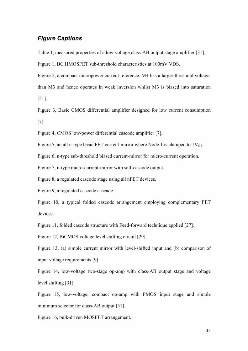
Figure Captions
Table 1, measured properties of a low-voltage class-AB output stage amplifier [31].
Figure 1, BC HMOSFET sub-threshold characteristics at 100mV VDS.
Figure 2, a compact micropower current reference. M4 has a larger threshold voltage.
than M3 and hence operates in weak inversion whilst M3 is biased into saturation
[21].
Figure 3, Basic CMOS differential amplifier designed for low current consumption
[7].
Figure 4, CMOS low-power differential cascode amplifier [7].
Figure 5, an all n-type basic FET current-mirror where Node 1 is clamped to 1VGS.
Figure 6, n-type sub-threshold biased current-mirror for micro-current operation.
Figure 7, n-type micro-current-mirror with self-cascode output.
Figure 8, a regulated cascode stage using all nFET devices.
Figure 9, a regulated cascode cascade.
Figure 10, a typical folded cascode arrangement employing complementary FET
devices.
Figure 11, folded cascode structure with Feed-forward technique applied [27].
Figure 12, BiCMOS voltage level shifting circuit [29].
Figure 13, (a) simple current mirror with level-shifted input and (b) comparison of
input voltage requirements [9].
Figure 14, low-voltage two-stage op-amp with class-AB output stage and voltage
level shifting [31].
Figure 15, low-voltage, compact op-amp with PMOS input stage and simple
minimum selector for class-AB output [31].
Figure 16, bulk-driven MOSFET arrangement.
45
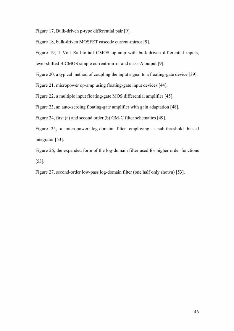
Figure 17, Bulk-driven p-type differential pair [9].
Figure 18, bulk-driven MOSFET cascode current-mirror [9].
Figure 19, 1 Volt Rail-to-tail CMOS op-amp with bulk-driven differential inputs,
level-shifted BiCMOS simple current-mirror and class-A output [9].
Figure 20, a typical method of coupling the input signal to a floating-gate device [39].
Figure 21, micropower op-amp using floating-gate input devices [44].
Figure 22, a multiple input floating-gate MOS differential amplifier [45].
Figure 23, an auto-zeroing floating-gate amplifier with gain adaptation [48].
Figure 24, first (a) and second order (b) GM-C filter schematics [49].
Figure 25, a micropower log-domain filter employing a sub-threshold biased
integrator [53].
Figure 26, the expanded form of the log-domain filter used for higher order functions
[53].
Figure 27, second-order low-pass log-domain filter (one half only shown) [53].
46
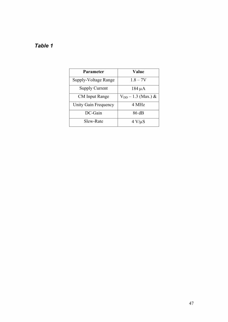
Table 1
Parameter Value
Supply-Voltage Range 1.8 – 7V
Supply Current 184 µA
CM Input Range VDD – 1.3 (Max.) &
Unity Gain Frequency 4 MHz
DC-Gain 86 dB
Slew-Rate 4 V/µS
47
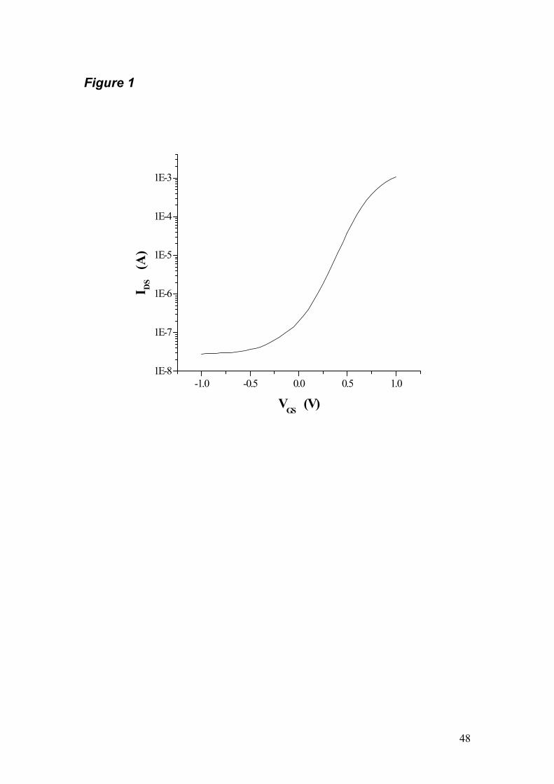
Figure 1
-1.0 -0.5 0.0 0.5 1.01E-8
1E-7
1E-6
1E-5
1E-4
1E-3
I DS
(A)
VGS (V)
48
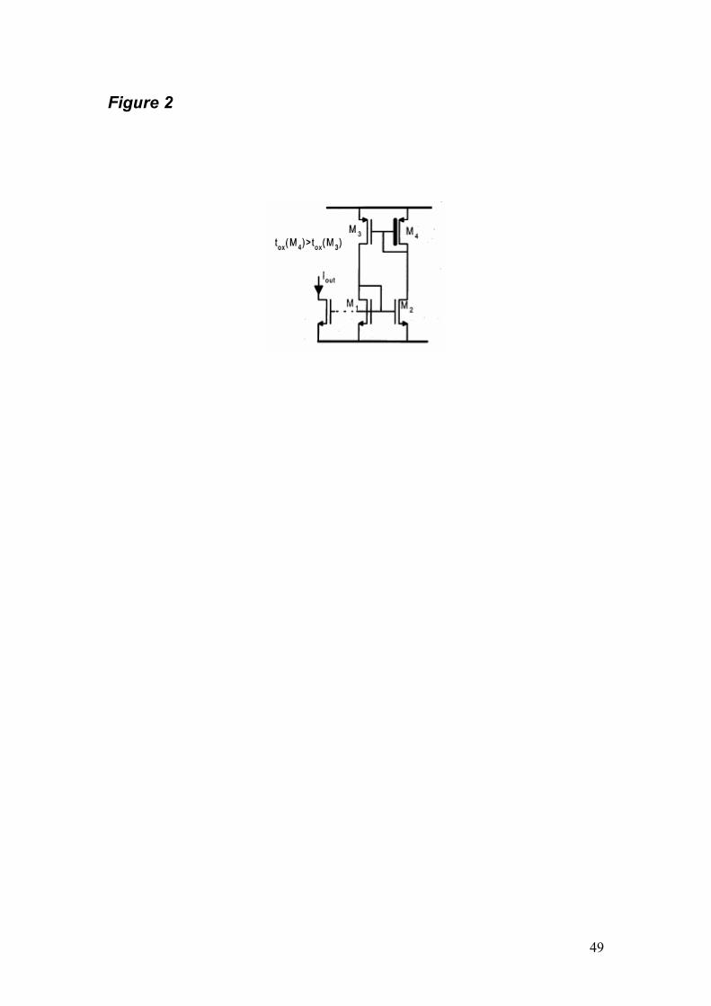
Figure 2
49
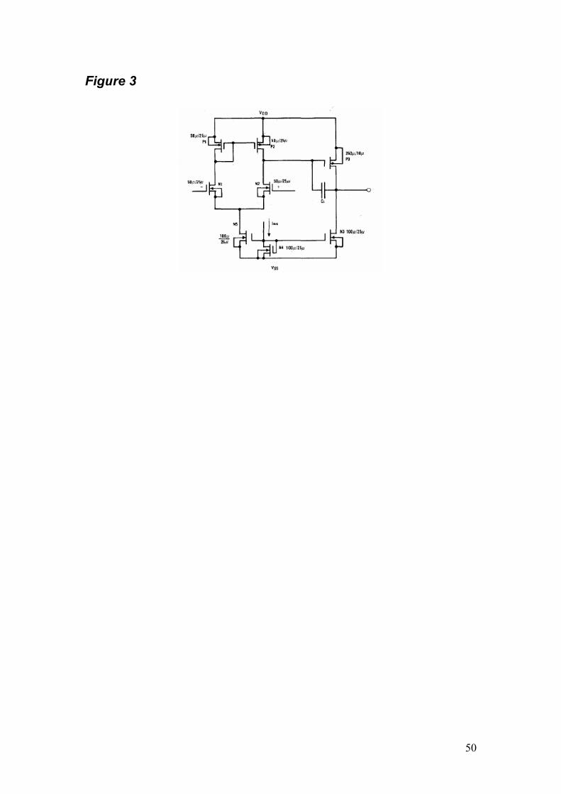
Figure 3
50
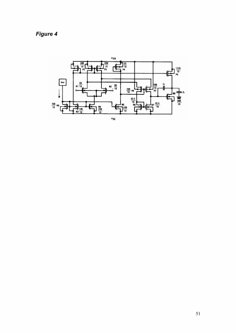
Figure 4
51
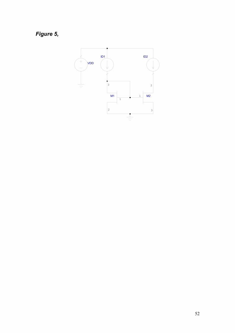
Figure 5,
1
2
3
1
2
3
VDD
ID1 ID2
M1 M2
52
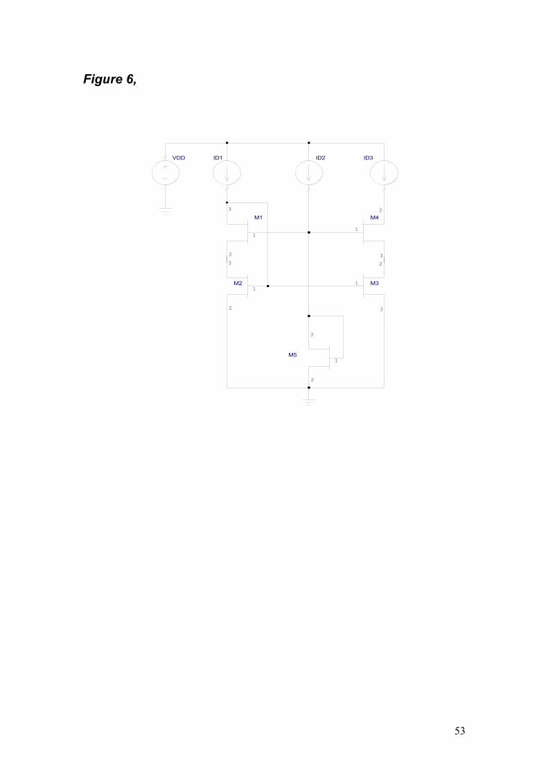
Figure 6,
1
2
3
1
2
3
1
2
3
1
2
3
1
2
3
VDD ID3
M3
M4
ID1
M2
M1
ID2
M5
53
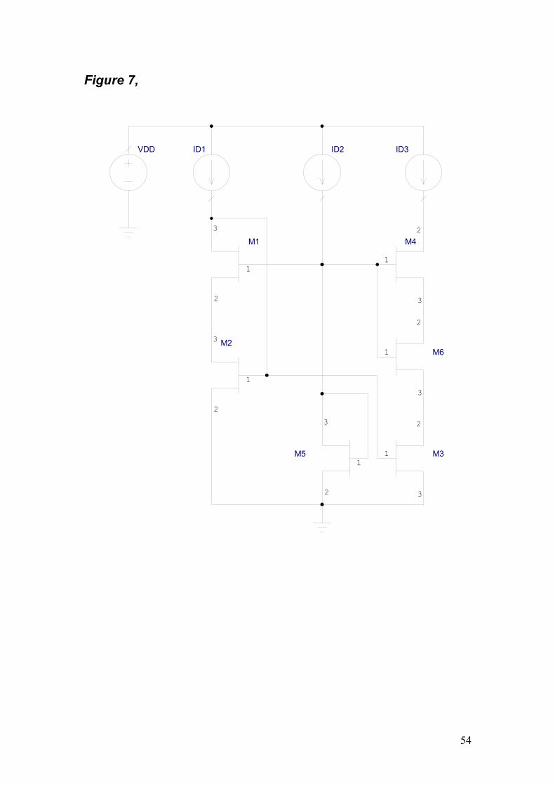
Figure 7,
1
2
3
1
2
3
1
2
3
1
2
3
1
2
3
1
2
3
VDD ID3
M3
M4
ID1
M2
M1
ID2
M5
M6
54
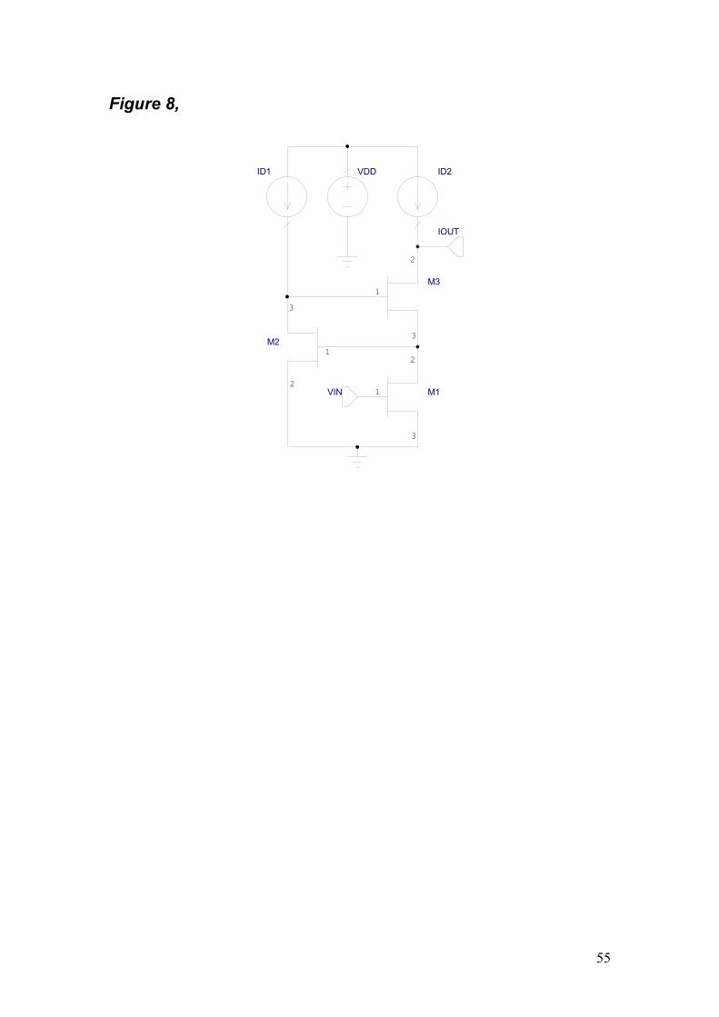
Figure 8,
1
2
3
1
2
3
1
2
3
ID2
M3
M1
VDDID1
M2
VIN
IOUT
55
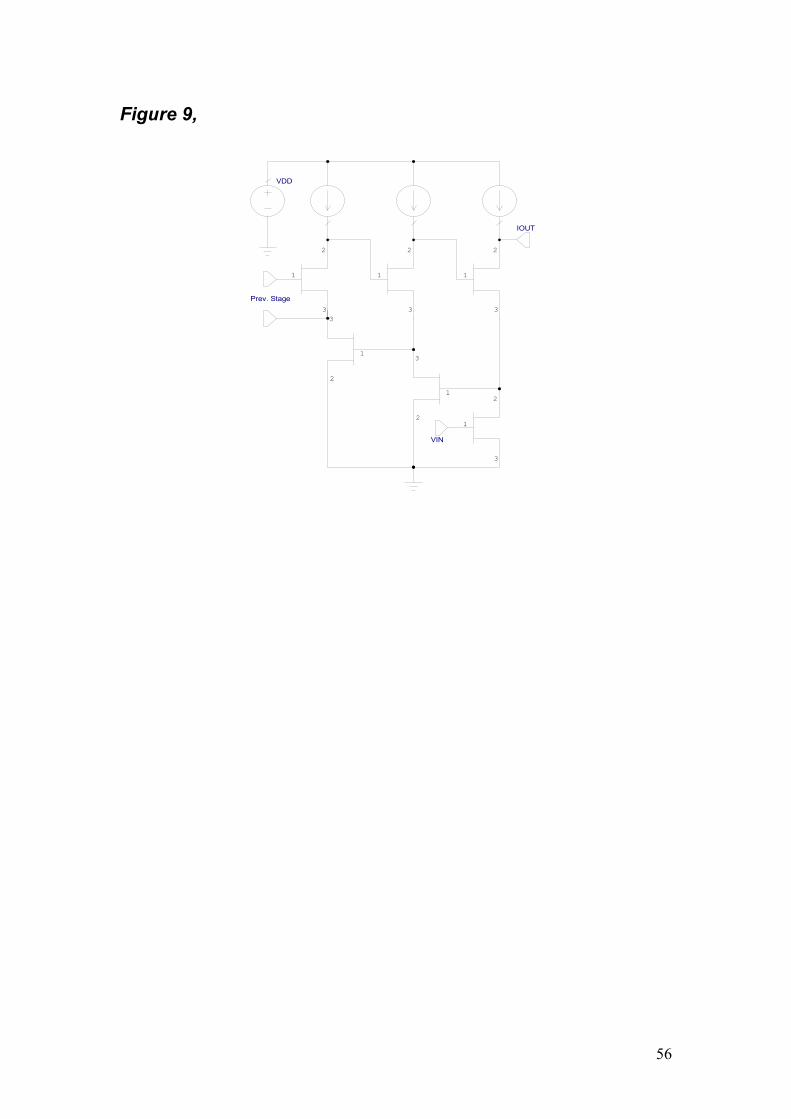
Figure 9,
1
2
3
1
2
3
1
2
3
1
2
3
1
2
3
1
2
3
Prev. Stage
VDD
VIN
IOUT
56
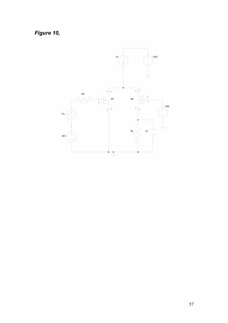
Figure 10,
G
D
S
1
2
3
G
D
S
1
2
3
VDD
VB2
VB1
Vin
Rin
ID
RL CL
M1 M2
57
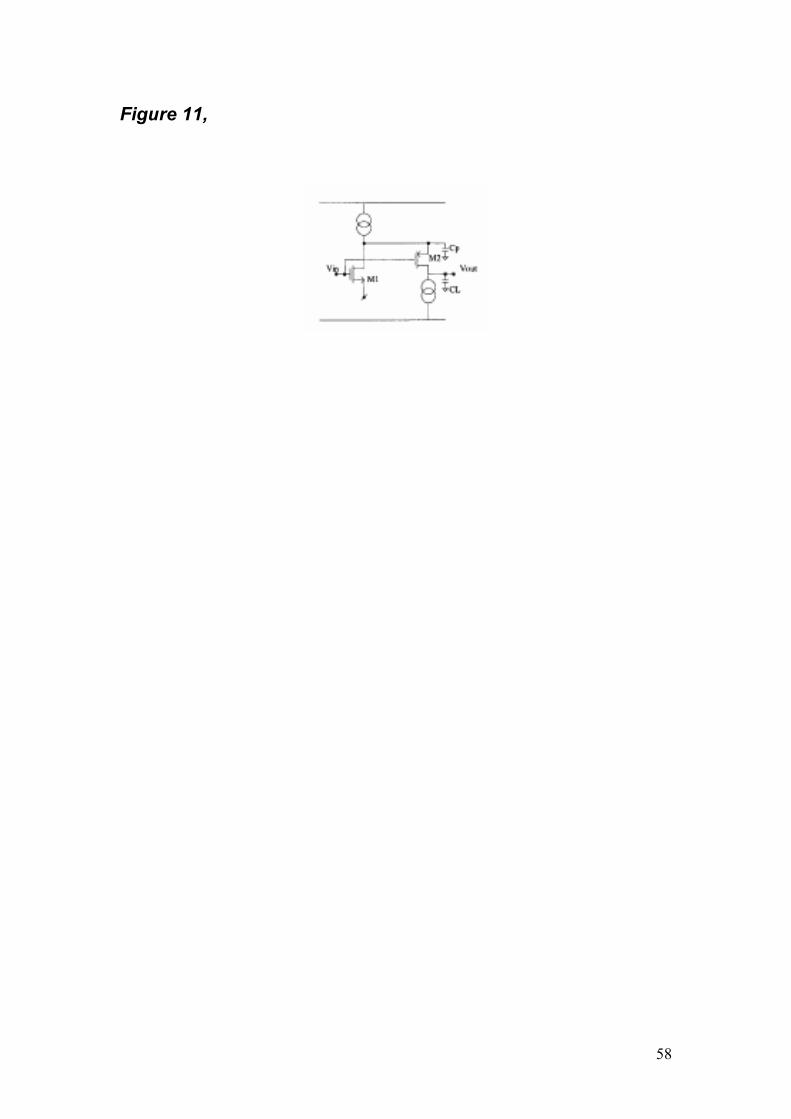
Figure 11,
58
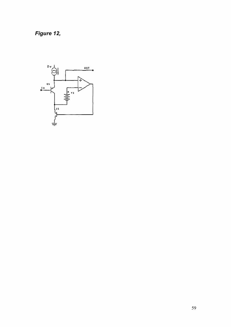
Figure 12,
59
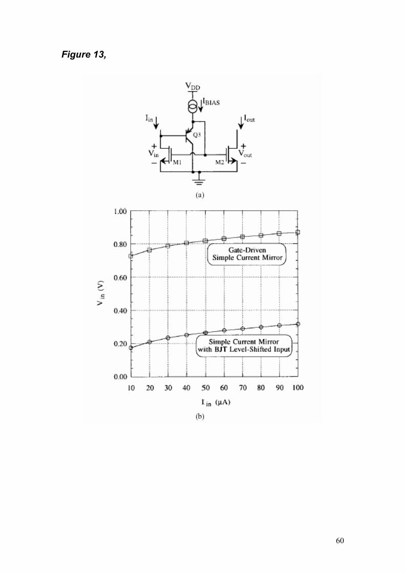
Figure 13,
60
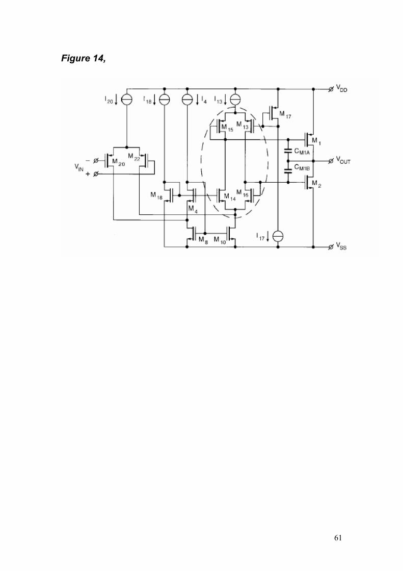
Figure 14,
61
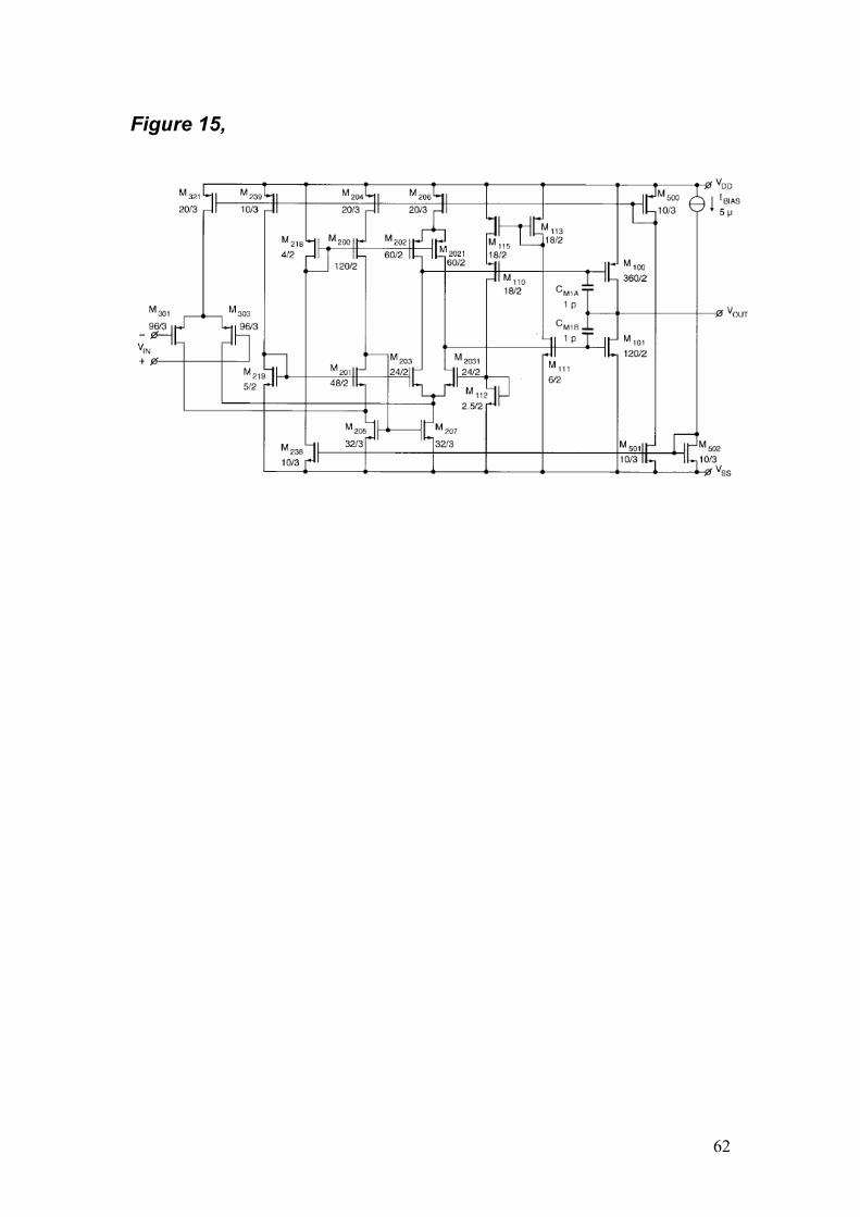
Figure 15,
62
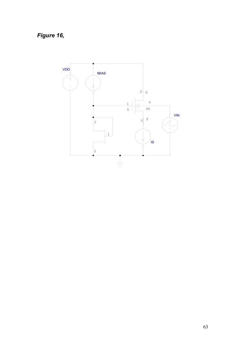
Figure 16,
G
D
S
SS1
2
3
4
1
2
3
VDDIBIAS
IS
VIN
63
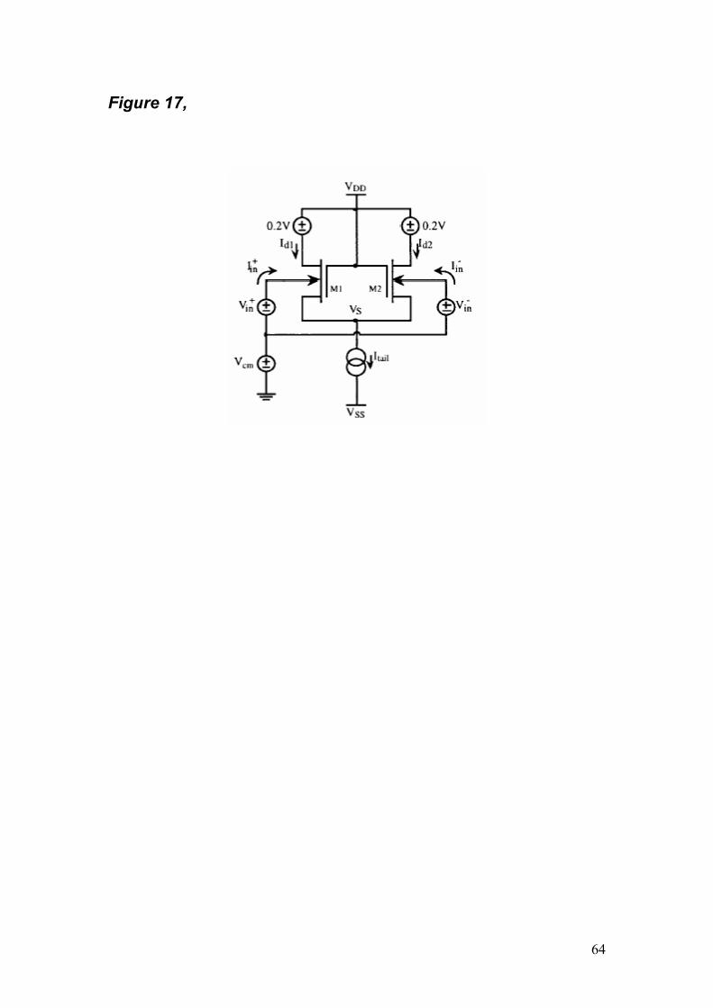
Figure 17,
64
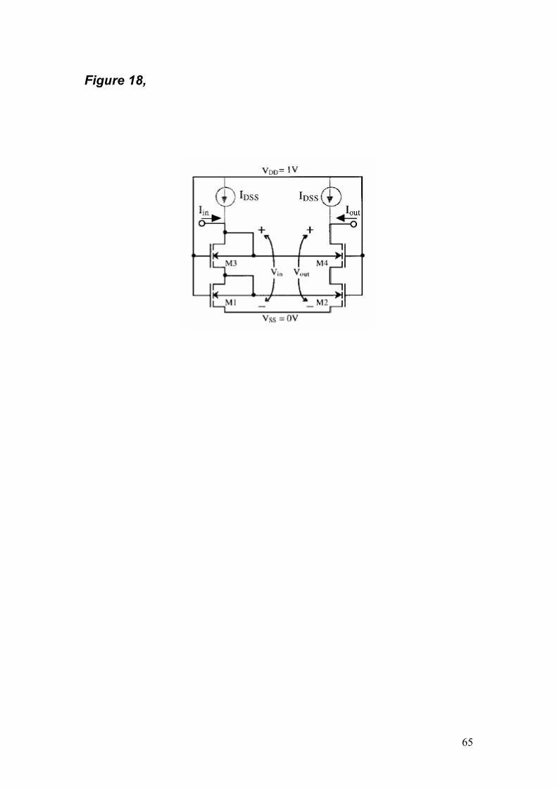
Figure 18,
65

Figure 19,
66
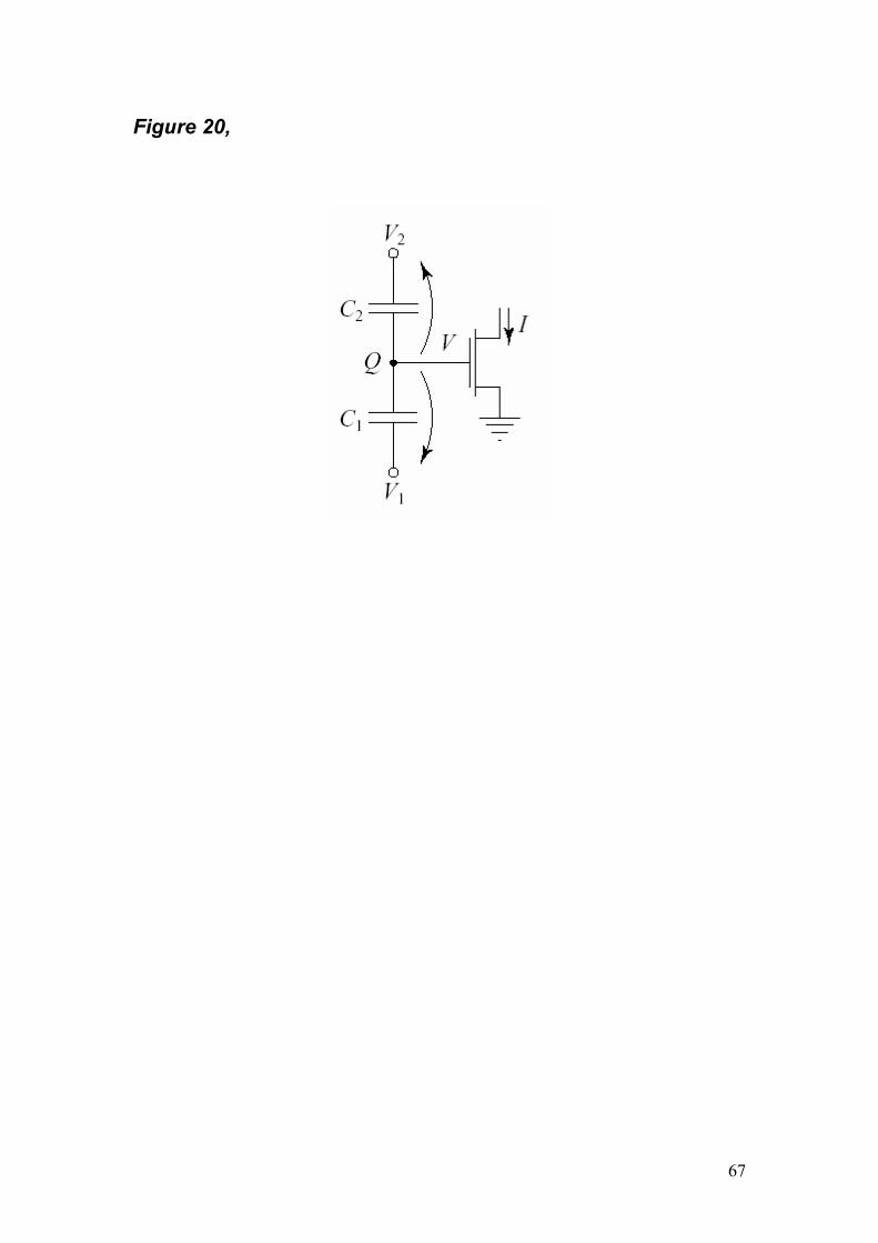
Figure 20,
67
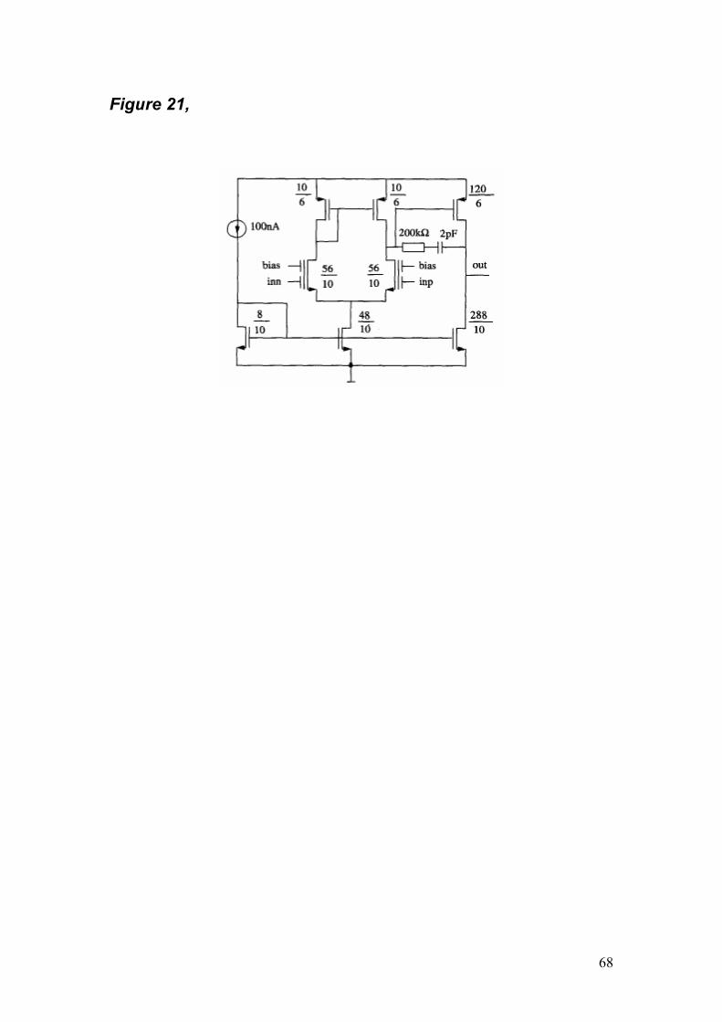
Figure 21,
68
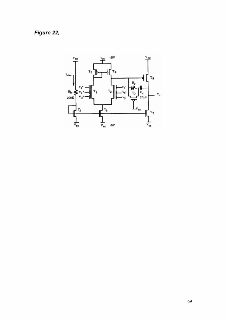
Figure 22,
69
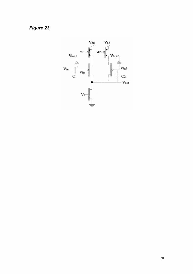
Figure 23,
70
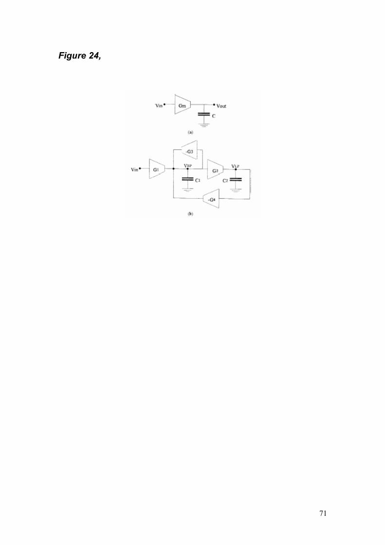
Figure 24,
71
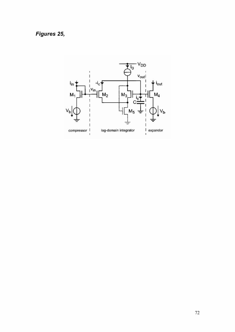
Figures 25,
72
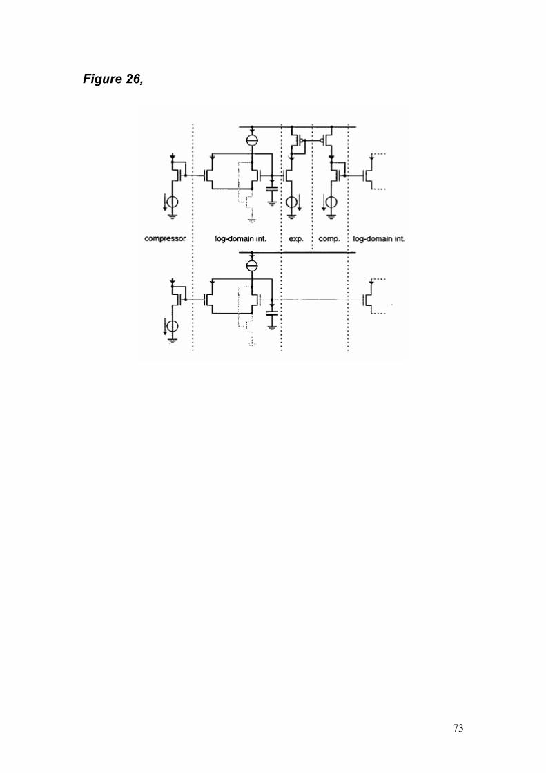
Figure 26,
73
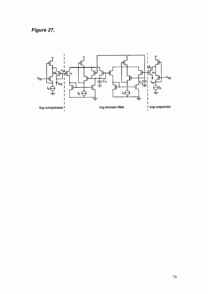
Figure 27,
74