
ANALOG SIGNAL PROCESSING CIRCUITS IN ORGANIC TRANSISTOR ...fk938sr9136/Dissertation... ·...
116
ANALOG SIGNAL PROCESSING CIRCUITS IN ORGANIC TRANSISTOR TECHNOLOGY A DISSERTATION SUBMITTED TO THE DEPARTMENT OF ELECTRICAL ENGINEERING AND THE COMMITTEE ON GRADUATE STUDIES OF STANFORD UNIVERSITY IN PARTIAL FULFILLMENT OF THE REQUIREMENTS FOR THE DEGREE OF DOCTOR OF PHILOSOPHY Wei Xiong October 2010
-
Upload
nguyenthuan -
Category
Documents
-
view
234 -
download
1
Transcript of ANALOG SIGNAL PROCESSING CIRCUITS IN ORGANIC TRANSISTOR ...fk938sr9136/Dissertation... ·...

ANALOG SIGNAL PROCESSING CIRCUITS IN
ORGANIC TRANSISTOR TECHNOLOGY
A DISSERTATION
SUBMITTED TO THE DEPARTMENT OF ELECTRICAL ENGINEERING
AND THE COMMITTEE ON GRADUATE STUDIES
OF STANFORD UNIVERSITY
IN PARTIAL FULFILLMENT OF THE REQUIREMENTS FOR THE DEGREE OF
DOCTOR OF PHILOSOPHY
Wei Xiong
October 2010

http://creativecommons.org/licenses/by-nc/3.0/us/
This dissertation is online at: http://purl.stanford.edu/fk938sr9136
© 2011 by Wei Xiong. All Rights Reserved.
Re-distributed by Stanford University under license with the author.
This work is licensed under a Creative Commons Attribution-Noncommercial 3.0 United States License.
ii

I certify that I have read this dissertation and that, in my opinion, it is fully adequatein scope and quality as a dissertation for the degree of Doctor of Philosophy.
Boris Murmann, Primary Adviser
I certify that I have read this dissertation and that, in my opinion, it is fully adequatein scope and quality as a dissertation for the degree of Doctor of Philosophy.
Zhenan Bao
I certify that I have read this dissertation and that, in my opinion, it is fully adequatein scope and quality as a dissertation for the degree of Doctor of Philosophy.
Robert Dutton
Approved for the Stanford University Committee on Graduate Studies.
Patricia J. Gumport, Vice Provost Graduate Education
This signature page was generated electronically upon submission of this dissertation in electronic format. An original signed hard copy of the signature page is on file inUniversity Archives.
iii

iv
Abstract
Low-voltage organic thin-film transistors offer potential for many novel
applications. Because organic transistors can be fabricated near room temperature,
they allow integrated circuits to be made on flexible plastic substrates. This physical
flexibility allows organic transistors to integrate with bendable organic displays,
polymeric muscles, and conformal sensors. Additionally, organic semiconductors are
inherently sensitive to specific molecules, making organic transistors naturally suited
for chemical and biological sensors. In all these applications, data converters are the
essential link between the digital processors and the analog media. However, because
of the inherent non-uniformities in organic processing, organic analog circuits suffer
from large variations that lead to inaccurate and unreliable data conversion. Dielectric
leakage and large parasitic capacitances further limit the available design space. This
dissertation describes the sources of these process handicaps and offers design
techniques to counter them. By applying these techniques, this research demonstrated
the world's first organic-transistor digital-to-analog converter and the first organic-
transistor analog-to-digital converter. Both data converters operate at 3 V, 100 Hz and
resolve 6 bits. Similar design methodology can be utilized in designing other organic-
transistor based analog signal processing circuits.

v
Acknowledgements
First, I would like to thank Professor Boris Murmann for advising my doctoral
research. I knew nothing about organic electronics, but Boris’s vision convinced me to
enter this field. Through his guidance, I was able to build truly novel devices. I very
much appreciate his generous support – never did I worry about lack of resources, and
cherish the freedom he gave – to try things, to ruminate, and to twiddle thumbs every
now and then. Most of all, I thank him for an enjoyable Ph.D. experience.
I thank my co-advisor, Professor Zhenan Bao, for being a constant source of
knowledge and support. Her lab had been instrumental in helping me finding my way
around organic transistors. She offered valuable advices on both organic electronics
and on the general science during the long shared drives to conferences, for which I
am greatly thankful.
I thank Professor Alberto Salleo for his help from Day 1 to Day 1800. He was
always available whenever I needed enlightenment on organic materials (or Italy). On
the first day, he helped me understand the basic polymer conduction; and on the 1800th
day, he advised me on career opportunities. In between, he sent me papers, offered his
lab equipment, and showed me how to properly measure organic transistors. I thank
him for all the help and for chairing my oral defense committee.

vi
I also thank Professor Bob Dutton for serving on my oral and reading committees,
and for showing me the genesis of some of the semiconductor theories, and how they
can apply to the organic transistors.
I am tremendously grateful to my collaborators, Drs. Hagen Klauk and Ute
Zschieschang of the Max Planck Institute for Solid State Research in Stuttgart,
Germany, for the fabrication of the organic transistors and circuits. Their work on
developing high-quality organic transistors was instrumental in achieving the circuit
performance cited in this dissertation. Especially, I thank Hagen for his experience and
optimism, and Ute for her dedication in making sure every transistor worked as best as
it could.
In addition to fabrication at the Max Planck Institute, much of the earliest
fabrication was performed and advised by Dr. Jim Kruger of Stanford Nano Fab.
Almost everything I knew about silicon fabrication I learned from Jim. These
knowledge would be constructive in developing the organic circuit processes. I’m very
grateful for Jim’s help.
I would like to thank the current and former members of Murmann Group and
Bao Group for useful discussions. In particular, I thank Alex Guo, who helped with
much of FPGA programming, Yoonyoung Chung, Echere Iroaga, Jason Hu, Clay
Daigle, Jim Salvia, Justin Kim, Pedram Lajevardi, Manar El-Chammas, Noam Dolev,
Alireza Dastgheib, Prastoo Nikaeen, Colin Reese, and Tony Sokolov.
On the personal side, I would like to thank my parents – for everything. They
always strived to achieve a better life for our family. It is through their hard work and

vii
dedication that I am in the position to complete this Ph.D. I will always remember
their love, care and inspiration. I also thank my brother for his love and support (and
free Google food). He took care many of our family tasks so I could focus on my
career and school. I could not ask for a better sibling.
I want to thank my grandparents – who took turns rearing me when my parents
were studying abroad. It’s often said that the Ph.D. is an exercise in perseverance.
Whatever perseverance I had, I inherited from them.
Finally, my deepest gratitude goes to my beautiful wife Cheryl. She put up with
some truly atrocious schedules – dinner at 10pm, not home until 3am; on more than a
few occasions our dates ended in the lab. She may not care for the difference between
a transistor and a capacitor, but her hugs and smiles made all the difference in the
world when things were going badly – and organic transistors went badly often. I
thank her being there for me, always.

viii
Table of Contents
Abstract ........................................................................................................................ iv
Acknowledgements ....................................................................................................... v
Table of Contents ....................................................................................................... viii
List of Tables ................................................................................................................. x
List of Figures .............................................................................................................. xi
1. Introduction .............................................................................................................. 1
1.1. Motivation ................................................................................................................................... 1
1.2. Background on Organic Semiconductors and Organic Transistors ...................................... 4
1.3. Research Goals ........................................................................................................................... 9
1.4. Organization ............................................................................................................................. 13
2. Organic Transistor Fabrication ............................................................................ 14
2.1. Fabrication at the Stanford Nano Fab ................................................................................... 14
2.2. Fabrication at the Max Planck Institute ................................................................................ 19
2.3. Special Circuit Layout Considerations................................................................................... 25
3. Effects of Organic Device Non-idealities on Analog Circuits ............................. 28
3.1. Device Mismatch ...................................................................................................................... 28
3.2. Large Parasitic Capacitances .................................................................................................. 33
3.3. Dielectric Leakage .................................................................................................................... 34
3.4. Modeling Inaccuracies ............................................................................................................. 37
4. Design of Organic DAC and ADC ........................................................................ 40
4.1. Design Limitations due to the OTFT Process ........................................................................ 41
4.2. DAC Design and Measurement ............................................................................................... 43

ix
4.2.1 DAC Architecture ........................................................................................................... 43
4.2.2 Calibration ...................................................................................................................... 49
4.2.3 Limits on DAC Operating Speed .................................................................................... 49
4.2.4 DAC Measurement ......................................................................................................... 53
4.3. ADC Design and Measurement ............................................................................................... 58
4.3.1 ADC Architecture ........................................................................................................... 58
4.3.2 Auto-zeroed Comparator Design .................................................................................... 63
4.3.3 Digital Logic Implementation ......................................................................................... 71
4.3.4 ADC Measurement ......................................................................................................... 74
5. Conclusion and Future Work ................................................................................ 79
5.1. Summary of This Dissertation ................................................................................................. 79
5.2. Future Work .............................................................................................................................. 81
5.2.1 Integration with Organic Sensors .................................................................................... 81
5.2.2 Packaging and Physical Interfaces .................................................................................. 82
5.2.3 Organic Transistor AM Radio ........................................................................................ 85
6. Appendix A .............................................................................................................. 87
6.1. Probe Station and Test Equipment ......................................................................................... 87
6.2. Interfaces between Probes and FPGA .................................................................................... 92
7. Appendix B: OTFT Model ..................................................................................... 93
References ................................................................................................................... 97

x
List of Tables
Table 1: Comparisons of typical organic transistors and inorganic transistors. ............ 9
Table 2: Some main OTFT parameters. ...................................................................... 22
Table 3: Summary of OTFT fabrication steps. ............................................................ 23
Table 4: Nominal OTFT parameters, calculated stage gains and settling times of the ADC comparator. .......................................................................................... 69
Table 5: Summary of ADC characteristics. ................................................................. 78
Table 6: Comparisons of this organic ADC and a silicon ADC. ................................. 78
Table 7: Fabrication layers with additional thick pads to facilitate wire bonding. ..... 84

xi
List of Figures
Figure 1: Unique advantages of organic transistors – flexibility, large-area printing, and chemical specificity. ................................................................................................ 3
Figure 2: Some conceptual applications of organic transistors – (clockwise from top left) a wearable mobile phone, smart bandages, artificial skin and retina, and an electronic newspaper. ..................................................................................................... 3
Figure 3: Hundreds of organic semiconductors. (Source: Bao research group.) ......... 4
Figure 4: Improvements in organic semiconductor mobility and corresponding example applications. (Source: Bao research group.) ................................................... 6
Figure 5: Chemical structures of the three organic semiconductors used in this work. (Sources: Wikipedia; Klauk research group; Bao research group.) ............................. 6
Figure 6: Illustrations of the bottom-gate top-contact and the bottom-gate bottom- contact structures. ........................................................................................................... 7
Figure 7: The top-contact OFET closely resembles the silicon MOSFET. ................... 8
Figure 8: State-of-art digital organic circuits, circa 2010 ............................................ 10
Figure 9: State-of-art analog organic circuit, circa mid-2009 ..................................... 11
Figure 10: General block diagram of a mixed-signal electronic system. .................... 12
Figure 11: An organic ADC (top half of the substrate) and an organic DAC (bottom half of the substrate) developed in this research. ......................................................... 12
Figure 12: Typical organic transistor fabrication procedures in the SNF. .................. 15
Figure 13: Photograph of the organic transistor and circuit structures on a PECVD oxide wafer, with linear and octagonal transistors at the right. .................................... 17
Figure 14: Photograph of a wafer with spin-on-glass as the dielectric. ...................... 18
Figure 15: Output curves of organic transistor fabricated at the SNF with 200 nm-thick cross-linked PVP dielectric, channel length = 100 μm, channel width = 2000 μm. ...................................................................................................................................... 18
Figure 16: Transfer curves of the organic transistor with cross-linked PVP dielectric, showing large hysteresis due to trapped charges in the dielectric. ............................... 19

xii
Figure 17: Cross-sectional view of an OTFT fabricated at the Max Planck Institute (not to scale) – the organic semiconductor can be either p-type or n-type, source and drain metals are gold, gate metal is aluminum (left); Photograph of an OTFT (right). 20
Figure 18: Measured output characteristics of an n-type OTFT (length = 20 μm, width = 400 μm) with VGS swept from 0 to 3 V in 0.5 V increments (left); Measured transfer characteristics of the same OTFT with VDS swept from 1 V to 3 V in 0.5 V increments (right). ........................................................................................................................... 22
Figure 19: Measured output characteristics of a p-type OTFT (length = 20 μm, width = 400 μm) with VGS swept from 0 to -3 V in -0.5 V increments (left); Measured transfer characteristics of the same OTFT with VDS swept from -1 V to -3 V in -0.5 V increments (right). ........................................................................................................ 23
Figure 20: Cross-sectional view of the capacitor, fabricated in the OTFT process (not to scale) (left); Photograph of two capacitors formed by intersecting traces (right). ... 24
Figure 21: Cross-sectional view of the layers of OTFT, via and capacitor (not to scale). ............................................................................................................................ 25
Figure 22: A gate-metal mask showing all traces in the vertical direction (left); A source-drain-metal mask showing all traces in the horizontal direction (right). .......... 26
Figure 23: Distributions of measured organic transistor drain-source currents, normalized to the mean. ............................................................................................... 29
Figure 24: Measured organic transistor drain-source currents, normalized to the mean, as a function of the transistor W/L ratios. The lines are the standard deviations of drain-source currents, for p-type (dash line) and n-type (solid line), respectively. L is constant at 20 μm. ........................................................................................................ 30
Figure 25: Distributions of measured capacitances, normalized to the mean. ............ 32
Figure 26: Illustration of an OTFT viewed from above, showing the gate overlaps (Loverlap) and the channel (L). ........................................................................................ 33
Figure 27: Measured and modeled leakage density of capacitors fabricated in the organic process, as a function of applied capacitor voltage. ........................................ 35
Figure 28: A typical switched-capacitor circuit with sample-and-hold operation and some leakage current (top); Modeled voltage errors due to leakage (bottom). ............ 37
Figure 29: Parameters of the OTFT model in Cadence Verilog-A. ............................ 38
Figure 30: Schematics of the OTFT model (left); The capacitor model (right). ......... 39
Figure 31: OTFT process characteristics limit the available design space. ................ 42

xiii
Figure 32: Current-steering DAC (top) and switched-capacitor DAC (bottom) architectures. ................................................................................................................. 42
Figure 33: C-2C structure on silicon suffers from parasitic substrate capacitances (top); The same C-2C structure on glass or plastic has no substrate capacitance (bottom). ....................................................................................................................... 45
Figure 34: Circuit schematic of the C-2C DAC; VREF = 3 V, VRESET = 1.5 V. ........... 46
Figure 35: Comparison of the unit capacitor matching (σu_DNL) and the corresponding unit capacitance required for C-2C and binary-weighted DACs in our organic process (for DNL = 1, yield = 95%). ......................................................................................... 48
Figure 36: Minimum DAC frequency required for 1-LSB output error due to capacitor leakage (8-bit and 10-bit are included for comparison). .............................................. 52
Figure 37: Measured DAC transfer function (before calibration) becomes increasingly nonlinear as the clock rate increases from 100 Hz to 500 Hz. ..................................... 54
Figure 38: Measured DAC output voltage error (code 63, before calibration) as a function of the clock rate; from top to bottom: 0.1 Hz, 0.5 Hz, 1 Hz, 2 Hz, 5 Hz and 10 Hz. ................................................................................................................................ 54
Figure 39: Ideal and measured (after calibration) DAC transfer functions at 100 Hz conversion rate. ............................................................................................................. 55
Figure 40: DAC DNL and INL before calibration [(a) and (b)] and after calibration [(c) and (d)]. ........................................................................................................................ 56
Figure 41: Spectrum of 10 Hz and 45 Hz DAC output sinusoids (500-point FFT). ... 57
Figure 42: Photograph of the C-2C DAC on glass substrate. ...................................... 58
Figure 43: SAR ADC, showing its main circuit blocks. ............................................. 59
Figure 44: C-2C structure with integrated sampling switches S0 – S5. The switches sample every clock cycle to prevent accumulation of leakage charges on the sampling capacitors C. ................................................................................................................. 61
Figure 45: ADC circuit with detailed C-2C DAC and calibration DAC schematics. . 61
Figure 46: Photograph of the ADC on the glass substrate. ......................................... 63
Figure 47: The comparator circuit and device parameters. ......................................... 64
Figure 48: Two-phase operation of the comparator. ................................................... 65

xiv
Figure 49: Measured transfer function (left) and small-signal gain (right) of an OTFT inverter, with Wp = Wn = 500 μm, Lp = Ln = 20 μm. ................................................... 66
Figure 50: Measured transient response of the first gain stage of a test comparator, showing a gain of ΔVout/ΔVin = -7.8 and a settling time of 13 ms. The clock rate was 30 Hz. ........................................................................................................................... 68
Figure 51: Anti-symmetrical layout of the inverter to maintain constant steady-state gain. .............................................................................................................................. 70
Figure 52: Cross-sectional views of the inverter in the nominal condition (top), with mask misalignment (bottom). ....................................................................................... 71
Figure 53: Conceptual diagram of the SAR algorithm. ............................................... 72
Figure 54: State machine of the SAR algorithm implementation. “CMP” is the comparison result between the DAC output and the sampled input, with “1” representing a larger input. ........................................................................................... 73
Figure 55: Timing diagrams of the main control signals. ........................................... 74
Figure 56: Measured comparator output and DAC output, showing that an input voltage had been converted to code 19. ........................................................................ 76
Figure 57: Measured ADC transfer function at 100 Hz sampling rate. ....................... 76
Figure 58: Measured ADC DNL and INL without calibration. .................................. 77
Figure 59: Measured ADC DNL and INL with calibration. ....................................... 77
Figure 60: The organic ADC integrated with organic sensors. ................................... 82
Figure 61: Unsuccessful attempts at wire bonding using aluminum (left) and gold (right) pads. ................................................................................................................... 83
Figure 62: Concept of an organic transistor AM radio receiver. ................................. 85
Figure 63: Drawing of the measurement apparatus. .................................................... 88
Figure 64: Photograph of the test setup. ...................................................................... 88
Figure 65: Photograph of the probe station. ................................................................ 89
Figure 66: CAD drawing of the probe wedge. ............................................................ 89
Figure 67: Photograph of the probe wedges mounted on the probe station. ............... 90
Figure 68: Photograph of a probe card. ....................................................................... 91

xv
Figure 69: The measurement apparatus with a probe card instead of probe wedges. . 91
Figure 70: Photograph of the adapter board (left) and the FPGA board (right). ......... 92
1
1. Introduction
This chapter provides an overview on organic transistors, their applications, and
the research conducted for this dissertation. Section 1 introduces some of the unique
properties of organic transistors and the potential applications. Section 2 summarizes
the structures and performances of organic transistors. Section 3 outlines our research
goals. Section 4 describes the organization of this dissertation.
1.1. Motivation
In the three decades since Alan J. Heeger, Alan G. MacDiarmid, and Hideki
Shirakawa discovered electrical charge transport in polymers [1], for which they
would win the Nobel Prize in chemistry in 2000, much progress had been made in
extending their groundbreaking discovery to practical applications. The invention of
the organic light-emitting diode (OLED) by Ching W. Tang and Steven Van Slyke in
1987 [2] further promoted the research of semiconducting polymers. Today, due to its
superior image quality and mechanical flexibility, OLED is poised to overtake liquid
crystal display (LCD) as the display of choice. As the two-terminal organic diodes
2
reach commercialization, the three-terminal organic transistors are transitioning from
scientific experiments to practical devices.
A number of structures exist for organic transistors, including the thin-film
implementation used in this work. The organic field-effect transistors (OFET) present
a new approach to building electronics that can mechanically flex, span large areas,
and integrate with organic materials. In particular, the recent development of low-
voltage complementary OFET provides a path to realize many novel applications. At
present, the most immediate application is flexible displays, with several
manufacturers demonstrating commercial prototypes [3] – [5]. In the near future,
OFETs may underpin devices ranging from large-area structural monitors to artificial
skin [6] – [8]. Because OFET can be manufactured at or near room temperature, they
allow integrated circuits to be made on flexible plastic substrates that do not withstand
the high processing temperatures used for silicon based devices. And because organic
materials can be made soluble [9] – [11], the ability to print organic OFETs advances
the prospect of inexpensive large-area electronics [9]. Furthermore, as most organic
semiconductors are sensitive to specific chemical or biological agents [12], OFETs
make excellent sensory receptors. This mechanical flexibility, large-area coverage,
and chemical specificity make OFETs naturally suited to integration with organic
materials such as artificial muscles [13], polymer actuators [14] and biochemical
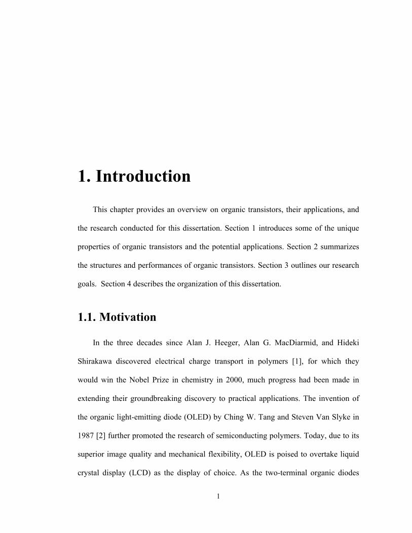
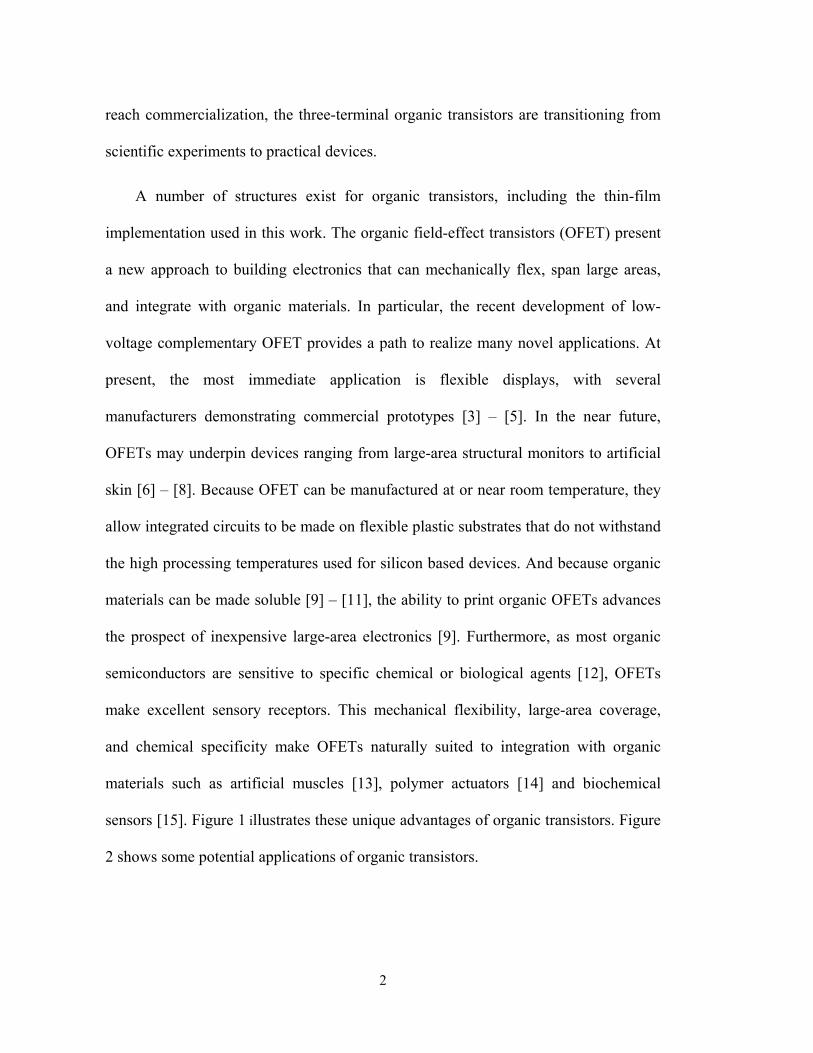
sensors [15]. Figure 1 illustrates these unique advantages of organic transistors. Figure
2 shows some potential applications of organic transistors.

3
Figure 2: Some conceptual applications of organic transistors – (clockwise from top left) a wearable mobile phone, smart bandages, artificial skin and retina, and an electronic newspaper.
Figure 1: Unique advantages of organic transistors – flexibility, large-area printing, and chemical specificity.

4
1.2. Background on Organic Semiconductors and Organic Transistors
Organic semiconductors comprise any semiconductor derived from hydrocarbon
based materials. The semiconductor can take the form of single-crystal,
polycrystalline, small molecules, or long polymeric chains [16]. Over the past twenty
years, hundreds of organic semiconductors have been discovered or synthesized; some
Figure 3: Hundreds of organic semiconductors. (Source: Bao research group.)
P-type:
N-type:
O
O
O O
O O
N
N
O O
O O
H
H
N
N
O O
O O
R1
R2
N
N
O O
O O
C7F15
C7F15
N
N
O
OO
O
CF3F3C
N
N
O O
O O
C3F7
C3F7
N
N
O O
O O
R
RNTCDA (v, 3x10⁻³, 1996)
R1 = CH2(CH2)7CH3 R2 = NH2 (v, 3x10⁻⁴, 2003) = CH2(CF2)6CF3 = NH2 (v, 2x10⁻⁴, 2003) = CH2(CF2)2CF3 = NH2 (v, N.O., 2003) = (CH2)7CH3 = N(CH3)2 (v, 10-5, 2003)
R = C8H17 (v, 0.16, 2000) = C12H25 (v, 0.01, 2000) = C18H37 (v, 5x10⁻³, 2000)
(v, 0.03, 2000) (v, 0.06, 2000)
(v, 0.12, 2000)
Naphthalene Diimides
NTCDI
C6F13SC6F13S S
SS
S SS
RR
O
O
SSSC6F13
OS
C6F13
O
C8F13C8F13 S
F
F
FF
F
S
F
F
FF
F
SSS
FF
FF
F
F
F
F
F
F
F
F
F
F
SSS
S
F
F
FF
F
O
O
O
O
F
F
FF
F
SS S C6F13
OS
C6F13
O
O O
SSS
S
O
O
O
O
xx = 1 (v, 0.059, 2004) = 1.5 (v, 0.026, 2004) = 2 (v, 10-3, 2004)
R = C6H13 (v, 0.1, 2005) = C6F13 (v, 0.6, 2005)
(v, 10-3, 2005)
x
x = 1 (v, 2x10⁻⁴, 2004) = 2 (v, 0.074, 2004) = 3 (v, 3.9x10⁻³, 2004) = 4 (v, 2.5x10⁻³, 2004)
(v, 0.08, 2003)(v, 0.45, 2005)(s, 0.21, 2005)
(v, 0.043, 2005)
Thiophene Based Oligomers
(v, 0.11, 2004)
O
F3C S
CF3S
CF3S
N
S
S
NF3CS
N
S
S
NF3C CF3
F3C
CF3
F3C SN
SN
S
CF3S
N
S
CF3
N
S
F3C
N
SN
S
S
CF3
N
S
F3C
N
SS
S
CF3S
F3C SS
CF3
NF3C
N
SS
F3C
N
S
CF3
N
S
(v, N.O., 2005)
(v, 3x10⁻³, 2005)
(v, 0.18, 2005)
(v, 0.3, 2005)
(v, N.O., 2005) (v, 1.83, 2005)
(v, 2.8x10⁻³, 2005)(v, 0.085, 2005)
(v, 0.018, 2005)(v, 0.025, 2005)
Trifluormethylphenyl-Based Oligomers
NS
NC8H17C8H17n
(s, 4.8x10⁻³, 2005)
C8H17 C8H17
O
N N
N N
O
OR
RO
R = 2' ethylhexyl (s, 2.2x10⁻⁸, 2004)
N
N
O
N
N
O
N
N
O
N
N
O
S
COONH4
n
nBBL (s, 0.1, 2003) BBB (s, 10-6, 2003)
(s, 0.7, 2001)
n
n
Polymeric Systems
KEY:• (Deposition Method, Mobility [cm2V-1s-1], Year)• v: vapor; sc: single crystal; s: solution• N.O.: Not Observed; N.A.: Not Available
OO
C60 (v, 0.56, 2003) PCBM (s, 0.2, 2005)
Fullerenes and Fullerene Derivatives
R
R
n
n= 0, R= H (v, 0.013, 2003)n= 0, R= C6H13 (v, 0.13, 2003)n= 1, R= H (v, 0.072, 2003)n= 1, R= C6H13 (v, 0.18, 2003)
SSR
R
R= H (v, 0.063, 2005)R= C6H13 (v, 0.5, 2005)
S
S
S
S
R
R'
(v, 0.12, 2005)
(sc, 0.02, 2004)
R= Cl; R'= H (sc, 1.4x10⁻⁴, 2004)R= Br; R'= H (sc, 0.3, 2004)R= Cl; R'= Cl (sc, 1.6, 2004)R= Br; R'= Br (sc, N.A., 2004)
(v, 0.1, 2002)(sc, 1.3, 2004)
(v, 0.5, 2005)
Anthracene Based
Tetracene Based
(v, 1.1, 2004)
R1 R2
R3
R4R5
R6
C12H25O OC12H25
C12H25O OC12H25
R1-6= H
(v, 1.4x10⁻⁴, 2005)
R1,2,4,5=H; R3,6= C6H13
(v, 0.011, 2005)
R1,4=H; R2,3,5,6= C6H13
(v, 0.012, 2005)
R1-6= C6H13
(v, 9.5x10⁻⁴, 2005)
R1-6= Ph-p-C12H25
(s, 0.001, 2005)
(s, 0.02, 2005)
Polycyclic Aromatic Hydrocarbons
CH3
CH3
O
O
O
O
CH3
CH3
O
O
SiR3
SiR3
R1
R2
R2
R1
F
F
X
X
F
F
X
X
SiiPr3
SiiPr3
(v, 0.05, 2005) (v, N.A., 2005) (v, N.A., 2005)
R= Me (s, 10-5, 2003)R= Et (s, 10-5, 2003)R= iPr (s, 0.4, 2003)
(v, 6, 2003)
X= H (v, 0.014, 2005)X= F (v, 0.045, 2005)
Pentacene Based
Quinones
R1,R2= Me (v, 0.3, 2003) R = Cl (v, N.O., 2003)R1= Me; R2= H (v, 2.5, 2003)R1= C6H13; R2= H (v, 0.251, 2003)
(v, 10-3, 2004)(sc, 15.4, 2004)(s, 0.7, 2005)
(v, 10-3, 2004)
Rubrene Derivatives
NH
HN R
R
R= H (v, 0.006, 2003)R= CH3 (v, 0.001, 2003)
(v, 5x10⁻⁴, 2003)R=
NH
HN
R
NH
N
NR
(v, 0.148, 2005)
S
SR R
S
S
SiR3
SiR3
S
S
S
S
S
S
S
S
S S
SC6H13 C6H13
S
S S
S
S
S
C6H13
C6H13
(v, 5x10⁻⁵, 2003)R= H (v, 0.038, 2005)
R=
R= H (v, 0.09, 1998)R= C6H13 (v, 0.15, 1998)R= C12H25 (v, 0.14, 1998)R= C18H37 (v, 0.06, 1998)
R= Me (s, N.A., 2005)R= Et (s, 1, 2005)R= iPr (s, 10-4, 2005)
(v, 0.04, 1997)
(v, 0.15, 1999)
Dihydrodiazapentacene Imidazolylquinoline
Thioacene
Bis- and oligo-(benzodithiophene)
(v, 1.6x10⁻², 2001)
(v, 10-3, 2001)
SSS
S
S
SS
S
S
SS
(v, 0.05, 2000) (v, 0.045, 2005)
Bis- and oligo-(dithienothiophene)
S
S
S
S
(v, 0.06, 2005) (v, 0.09, 2005)
Substituted Fused-Bithiophene
N
N
R2
R2
R1
R1
NC6H13
Ph Ph
(v, 10-6, 2004)
S
NS
N
S
S
R
R (v, 0.003, 2004)S S C6H13
R= H (v, N.O., 2004)
O S
N
(v, 0.02, 2004) (v, 0.002, 2004) (v, N.O., 2004)
R
R
N
N
N
N
C12H25
C12H25
R2
R1
R2
R1
N
C8H17
C8H17
CH3
H3C
N
R= octyl (v, 0.003, 2005)R= dodecyl (v, 1.2x10⁻⁴, 2005)R= 4-octylphenyl (v, 0.12, 2005)R= 4-methylphenyl (v, 10-5, 2004)
R1= Cl, R2= H (v, 0.01, 2005)R1= H, R2= Cl (v, 0.14, 2005) (s, 0.002, 2005)
(v, 0.001, 2004)
R1= H, R2= C6H13 (v, 0.30, 2005)R1= C6H13, R2= CH3 (v, 0.054, 2005)
Carbazole Derivatives
Thiophene-Thiazolothiazole Co-Oligomers
SS
S
S
SS
DT-TTF(sc, 1.4, 2004)
S
S
S
S
S
S
S(sc, 0.062, 2004)
S S
S
S
SS
S
S
(sc, 0.0012, 2004)
S
S
S
SS
X2X1
X1= S, X2= H (sc, 0.4, 2004)X1= H, X2= S (sc, 0.015, 2004)
S
S
S
SX2X1
SX1= H, X2= S (sc, 1.8x10⁻³, 2004)X1= S, X2= H (sc, 1.4x10⁻⁴, 2004)
S
S
S
S
X
XX
X
X= C (v, 0.06, 2005) = N (v, 3.3x10⁻⁵, 2005)
S
S
S
S
X
XX
XX= C (v, 0.42, 2005) = N (v, 0.2, 2005)
TTF Derivatives
NS
NN
N
S
S S
S
S
(v, 0.2, 2004)
NS
NNS
N
SS
S S
(v, 3x10⁻⁴, 1978) BenzoBTQBT
N
NSe
SS
S S
R R
R R
R= H (v, N.O., 1978) = Benzo (v, 2x10⁻⁴, 1978)
NS
N
SS
S S
R R
R R
NS
N
SS
S S
R R
R R
SS
S S
X
X
R= H (v, N.O., 1978) = Benzo (v, 8x10⁻⁵, 1978)
X= C (v, N.O., 1978) = N (v, 6x10⁻⁷, 1978)
R= H (v, N.O., 1978) = Benzo (v, 2x10⁻⁶, 1978)
Bis(1,3-dithiol-2-ylidene) Compounds with Conjugated Spacer
BTQBT
SeSe
SeSe
(v, 0.0036, 2003)X
X
X= S (v, 0.081, 2004)X= Se (v, 0.17, 2004); (sc, 1.5, 2005)X= Te (v, 0.0073, 2004)
Chalcogenophenes
C6H13
H
HH
S
SS
C6H13C6H13
C6H13 C6H13
C6H13
n n
n
N
N
R
R
RN
N
N
N
N
N N
R
RR
C10H21
S
S
C10H21
SS
S
S
SS
C10H21
S
R=
R=
R=
(s, 10-4, 2005)
(s, 10-4, 2005)
(s, 10-4, 2005)
(s, 2x10⁻⁴, 2003)
n= 1 (s, 1.03x10⁻³, 2005) = 2 (s, 6.5x10⁻⁴, 2005) = 3 (s, 2.2x10⁻⁴, 2005)
(s, 3x10⁻⁴, 2005)
Triarylamines
Oligothiophenes
NH
NH
N
NH
HN
HN
N
HN
H2SO4
N
N
N
NPt
N
N
NH
HN
(s, 2.2x10⁻⁴, 2003)(s, 0.68, 2005)(s, 0.012, 2003)
Porphyrins N
NNNNN
N N
N
NNN
NNN N
O O
OC8H17OC8H17
OO
C8H17OC8H17O
MC8H17
C8H17
C8H17
C8H17
M= Tb (s, 6.4x10⁻⁴, 2005) = Lu (s, 1.7x10⁻³, 2005)
MN
NN
N
N
NN
N
N
N N
N
R
But
But
tBu
M
NNNN
NNN
N
OOO
OO
OOO O
OO
O OO
O
O OOO
O
NNNN
NNN NO
OOO
O
OOO O O
OO O
OO
O OOOO
N
NNNNN
N N
O O
OC8H17OC8H17
OO
C8H17OC8H17O
C8H17C8H17
C8H17
C8H17M
M
M= Eu (s, 0.6, 2005) = Ho (s, 0.4, 2005) = Lu (s, 0.24, 2005)
M = Cu (v, 0.02, 1996) (sc, 1, 2005) = Sn (v, 3.4x10⁻³, 1997) = H2 (v, 2.6x10⁻³, 1997) = Zn (v, 2.8x10⁻³, 1997 = Fe (v, 6.9x10⁻⁴, 1997) = Pt (v, 1.5x10⁻⁴, 1997) = Ni (v, 5.4x10⁻⁵, 1997)
R= O(CH2)10OH; M= Cu (s, 4x10⁻⁴, 2003) = O(CH2)10OH; M= none (s, 4.8x10⁻⁵, 2003) = NH2; M= none (s, 10-6, 1999)
Phthalocyanines
SS
SS S
SSS
S
SSS
SS
S SSS
SS
SSS
SS
S C6H13C6H13S
SS
S RR
SSS
SS RR
SSS
SSR
S R
SSS
SS
SSS
R R
S
C6H13
SS
C6H13
R= CH3 (v, 9.2x10⁻³, 2004) = C10H21 (v, 0.5, 2003) = C6H13 (v, 0.054, 2004)
R= C2H5 (v, 1.1, 2003) = C6H13 (v, 1, 2003) = C10H21 (v, 0.5, 2003) = C12H25 (v, 0.016, 1998) = C18H37 (v, 1.3x10⁻³, 1998)
R = C6H13 (v, 0.03, 1997)
n
n= 3 (v, 0.012, 2004) = 4 (v, 0.064, 2004)
R= C6H13 (v, 0.23, 1998) = C10H21 (v, 0.2, 2003) = cyclohexyl (v, 0.038, 2005) (s, 0.06, 2005) (s, 4x10⁻⁴, 2004)
SSS
SS
S
SC4H9
C4H9S(v, 10-4, 1999)
SButMe2Si SiMe2But
n
4T (v, 0.014, 2004) 5T (v, 0.078, 2004)
6T (v, 0.07, 2003) (sc, 0.1, 1996)
8T (v, 0.2, 2003)
Unsubstituted Thiophenes
Alkyl-Substituted Thiophenes
n= 4 (v, 8x10⁻⁶, 1998) = 5 (v, 3x10⁻⁴, 1998) = 6 (v, 4x10⁻⁵, 1998)
SS
O
O
(v, N.O., 2004)
SS
SS RR S
SSS
SRS R
SC6H13 C6H13
S
C6H13 C6H13
SS
SS R2R1S
SSR RS
SR R
SSS
SS RR
SS
SS
SS
SS C6H13
SS
SS
R2R1
OS
O O
O
O On
R= (CH2)3OC4H9 (v, 0.033, 1998); (s, 0.01, 1998) = (CH2)3OC8H17 (v, 9x10⁻³, 1998); (s, 1x10⁻³, 1998) = (CH2)4PO(OEt)2 (s, 4.9x10⁻³, 2002)
R= (CH2)3OC4H9 (v, 8x10⁻³, 1998) (s, 3x10⁻³, 1998)
nn= 1 (s, 0.01, 2003) = 2 (s, 0.09, 2003) = 3 (s, 0.054, 2003) = 4 (s, 0.09, 2003)
R= tolyl (v, 0.03, 2004) = biphenyl (v, 0.17, 2003) = phenyl (v, 3x10⁻³, 2001)
R= phenyl (s, 1.4x10⁻³, 2003) = biphenyl (v, 7.7x10⁻³, 2003) (sc, 0.66, 2002)
R= tolyl (v, 0.02, 2004)
R1, R2= phenyl (s, 0.033, 2001)R1, R2= biphenyl (v, 0.055, 2003)R1, R2= tolyl (v, 0.03, 2004)
(s, 0.018, 2003)(v, 0.011, 2004)
R1= H, R2= C6H13 (v, 0.02, 2004) (v, 0.011, 2004)
Polar-Substituted Thiophenes
Thiophene-Fluorene Oligomers
Aromatic-Substituted Thiophenes
Asymmetric End-Capped Thiophenes
6 n(s, 10-4, 2003)
SR R
n= 1, R= C6H13 (v, 0.012, 2003)n= 2, R= C6H13 (v, 0.14, 2003)n= 3, R= C6H13 (v, 0.025, 2003)n= 4, R= C6H13 (v, 0.023, 2003)n= 2, R= H (v, 0.08, 2003)n= 2, R= cyclohexyl (v, 0.17, 2005)
n
SSR1
SR2 R1S
S
S
SS S
S SC6H13 C6H13
SS
N
S S
NS
SC6H13 C6H13
R R
SSO
SS
SS S
S SS
SC6H13
C6H13
SS
N
S
NSR R
SS S SR1R1
R2 R2
R2 R2
R2 R2
R2 R2
SS
S
SS
SS
NS
S SR
R
R1= H, R2= phenyl (s, 5x10⁻⁴, 2005)R1= C6H13, R2= phenyl (v, 0.042, 2005)R1= C10H21, R2= phenyl (v, 0.3, 2005)R1= C6H13, R2= biphenyl (v, 0.049, 2005)R1= C6H13, R2= flourene (v, 0.01, 2005)R1= C6H13, R2= flourenone (v, 2x10⁻³, 2005)R1= C6H13, R2= phenanthrene (v, 0.067, 2005)R1= H, R2= thiazole (s, 7x10⁻³, 2001)
R= H (v, 0.011, 1999) = C6H13 (v, 3.5x10⁻⁴, 1999)
R= H (v, 10-5, 1999) = C6H13 (v, 2x10⁻⁵, 1999)
(v, 5x10⁻⁴, 2001)
(v, 8x10⁻⁴, 2004)
(v, N.O., 2004)
(v, 0.02, 2004)
R1, R2= H (v, 1.4x10⁻³, 1997)R1= C6H13, R2= H (v, 0.055, 2003)R1= H, R2= C6H13 (v, 1.1x10⁻⁶, 2003)
R= H (s, 0.02, 2001) = C6H13 (s, 0.054, 2003)
(s, 10-4, 2001)
(v, 0.012, 1997)(s, 1.4x10⁻³, 1997)
Thiophene Core Substitutions
Alternating Co-Oligomers
S
OO
C12H25
S
n
OC12H25
SS
OC12H25
S
O
O
Sn
(s, 0.07, 2005)(s, 6.3x10⁻³, 2005)
S
NO
n
SS
C12H25
C12H25
n
SS
C8H17
C8H17
S n
SS
S S
R Rn
SS
S
C8H17 C8H17
nS
S
C8H17 C8H17
S
n
Bu
Bu
Bu Bu
SSiS
SS
S
2m m n
SSiS
SS
SBu
Bu
Bu Bu
m2 2n2
S n
OHO
S n(s, 2.9x10⁻⁴, 1999)
SS
SS
C12H25
C12H25
n
S S
R R
S S
RR
S S
C6H13 C6H13
S
C6H13
S S
C6H13 C6H13
S
C6H13
Regioregular P3HT (s, 0.12, 2004) Regiorandom P3HT
head-to-tail (HT)
head-to-head (HH)
poly(3-hexylthiophene) P3HT
(s, 10-3, 1999) (s, 2.8x10⁻⁵, 1999)
(s, 6x10⁻⁴, 2005)
(s, 0.03, 2005)
R = C8H17 (s, N.A., 2005) = C10H21 (s, 0.6, 2005)) = C12H25 (s, 0.12, 2005)
PQT-12 (s, 0.14, 2004)
3',4'PTT-8 (s, 0.01, 2004)3,3"PTT-8 (s, 0.03, 2005)
n
m= 2 (s, 3.4x10⁻⁵, 2005) = 3 (s, 4.6x10⁻⁵, 2005)
m= 2 (s, 6.9x10⁻⁵, 2005) = 3 (s, 6.7x10⁻⁵, 2005)
S n
Thiophene-Based Polymers
S
R
n
R= C4H9 (s, 1.2x10⁻³, 2005) = C8H17 (s, 3x10⁻⁴, 2005) = C10H21 (s, 8.5x10⁻⁵, 2005) = C12H25 (s, 2.4x10⁻⁵, 2005)
S SS S
S
C6H13
C6H13 F F
F F
C6H13
C6H13
n
(s, 2x10⁻³, 2005)
OR1OR2
R1OR3O nn
C8H17C8H17
n
C8H17 C8H17
S
S n
F8TT (s, 1.1x10⁻³, 2005)F8T2
(s, 0.02, 2004)
S
N
n
SN
S
C9H19
n
SNN
S nS S
R1R1
R2R2
nS S
R1R1
n
RR
n
R1= CH3, R2= C18H37, R3= H (s, 10-4, 2005)
R1= CH3, R2,3= 3,7-dimethyloctyl (s, 10-3, 2005)
R1,2= C11H23, R3= C18H37 (s, 0.01, 2005)
R= CH3 (s, 4x10⁻⁴, 2005) = 3,7-dimethyloctyl (s, 10-3, 2005)
O
RO n
O
NC6H13
n
O
NC6H13
S
C6H13n
N
n
(s, 2.5x10⁻³, 2004) (s, 3.4x10⁻⁴, 2005)
(s, 6x10⁻⁴, 2005)
(s, 3x10⁻³, 2004)
Poly(9,9'-dioctyl-flourene-co-bithiophene)
Thiophene-Thiazole/Thiadiazole Co-Polymer
Cyclopentadithiophene Based Polymers
R1=H, R2= C8H17 (s, 5x10⁻⁶, 2003)R1, R2= C8H17 (s, 10-7, 2003)
R= C8H17 (s, 7.9x10⁻⁵, 2003)
R= C6H13 (s, 4x10⁻⁴, 2004) = C8H17 (s, 10-3, 2004) = C10H21 (s, 2x10⁻³, 2004)
Poly(alkylidene fluorene) Poly(p-phenylene vinylene) (PPV)
(x=0.25) (s, 6x10⁻⁶, 2005)(x=0.50) (s, 3x10⁻⁴, 2005)(x=0.75) (s, 2x10⁻⁴, 2005)
(s, 9x10⁻⁶, 2005)
(s, 8x10⁻⁵, 2004)
Phenoxazine Based Polymers Polytriarylamines
(s, 0.01, 2004)
SS
C8H17C8H17
S
NSN
NN
S n
O
NC6H13
n
x
1-x
C6H13C6H13
(v, 7x10⁻⁵, 2005) (v, 7x10⁻⁵, 2005)
N
NN
N N N
N N
H3C CH3
H3C CH3
Spiro-Linked Compounds
C8H17
C8H17(v, 0.12, 2004)
Oligo(arylvinylene)
SiR3Me3Nn
Oligo(arylacetylene)Oligo(aryl)
n= 2 (4P) (v, 0.01, 1997)n= 3 (5P) (v, 0.04, 1997)n= 4 (6P) (v, 0.07, 1997)
R= CH3 (v, 0.3, 2005)R= iPr (v, 4.3x10⁻⁴, 2005)
N
NN N
NN
NN
MM = Lu (v, 10-4, 1990) = Tm (v, 10-4, 1990)
OO
O
O
O
O
N N
O
O
O
O
RR
NN
O
O
O
O
R R
CN
NC
(v, N.O., 2002) PTCDA (v, 10-4, 1997) R = C5H11 (v, 0.06, 2004) = C8H17 (v, 1.3, 2004) = C12H25 (v, 0.5, 2004) = C13H27 (v, 0.6, 2005) = C6H5 (v, 1.5x10⁻⁵, 1996)
R = (v, 0.1, 2004) (s, 10-5, 2004)
= n-CH2C3F7(v, 0.64, 2004)(s, 10-4, 2004) = (v, 1.9x10⁻⁴, 2005)
Perylene Diimide Derivatives
CN
CNNC
NCCN
CNNC
NC
S
RR
S SCN
CN
NC
NC
N
N
N
N CN
CN
R1
R2
R3R4
N
N
N
NNC
NC
N
N
N
N CN
CN
(v, 10-5, 1994) TCNQ (v, 10-3, 1994)
R1 = R2 = R3 = R4 = H (v, 3.6x10⁻⁶, 2004)
R1 = R4 = HR2 = R3 = CH3
R1 = R4 = HR2 = R3 = OCH3
R1 = R4 = OCH3
R2 = R3 = H
(v, 2.2x10⁻⁶, 2004)
(v, 9.6x10⁻⁷, 2004)
R = C4H9 (v, 0.2, 2003)
Quinoid Systems
(v, 10-8, 2004)
(v, 2.1x10⁻⁷, 2004)
(v, 2.5x10⁻⁷, 2004)
N
NN
N
N
N
N
NM
RR
R
R
R R
R
R
R
R
RR
R
R
R R
N
NN
N
N
N
N
NCu
RR
RR
R = F, M = Cu (v, 0.03, 1998)R = F, M = Zn (v, 1.2x10⁻³, 1998)R = F, M = Co (v, 4.5x10⁻⁵, 1998)R = F, M = Fe (v, 2.1x10⁻³, 1998)R = Cl, Me = Fe (v, 2.7x10⁻⁵, 1998)
R = SO3Na (s, 3x10⁻⁴, 2003)
Phthalocyanines
N
NN
N
N
N
N
NCu
R R
RR
NCl-
R =+
(s, 3x10⁻⁴, 2003)
S
S
R
R
S S C6H13 SS
(v, 3x10⁻⁴, 2005)(v, 10-4, 2005) (v, 0.006, 2005)
(v, 0.11, 2005)(v, 0.036, 2005)(v, 0.057, 2005)
Naphtha[1,8-bc:5,4-b'c']dithiophene
R =
R =
5
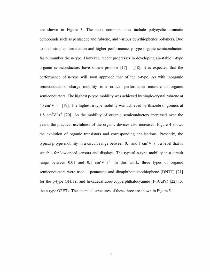
are shown in Figure 3. The most common ones include polycyclic aromatic
compounds such as pentacene and rubrene, and various polythiophenes polymers. Due
to their simpler formulation and higher performance, p-type organic semiconductors
far outnumber the n-type. However, recent progresses in developing air-stable n-type
organic semiconductors have shown promise [17] – [18]. It is expected that the
performance of n-type will soon approach that of the p-type. As with inorganic
semiconductors, charge mobility is a critical performance measure of organic
semiconductors. The highest p-type mobility was achieved by single-crystal rubrene at
40 cm2V-1s-1 [19]. The highest n-type mobility was achieved by thiazole oligomers at
1.8 cm2V-1s-1 [20]. As the mobility of organic semiconductors increased over the
years, the practical usefulness of the organic devices also increased. Figure 4 shows
the evolution of organic transistors and corresponding applications. Presently, the
typical p-type mobility in a circuit range between 0.1 and 1 cm2V-1s-1, a level that is
suitable for low-speed sensors and displays. The typical n-type mobility in a circuit
range between 0.01 and 0.1 cm2V-1s-1. In this work, three types of organic
semiconductors were used – pentacene and dinaphthothienothiophene (DNTT) [21]
for the p-type OFETs, and hexadecafluoro-copperphthalocyanine (F16CuPc) [22] for
the n-type OFETs. The chemical structures of these three are shown in Figure 5.

6
Among the many structures devised for OFETs, the most common ones are the
bottom-gate top-contact, and the bottom-gate bottom-contact [23]. Figure 6 shows the
physical differences between these two structures. Typically, the top-contact structure
achieves higher mobility than the bottom-contact. The exact mechanism of superiority
Figure 5: Chemical structures of the three organic semiconductors used in this work. (Sources: Wikipedia; Klauk research group; Bao research group.)
Figure 4: Improvements in organic semiconductor mobility and corresponding example applications. (Source: Bao research group.)
High speed IC
Displays, Sensors
E-paper, Solar cells
Low speed IC
1986 1988 1990 1992 1994 1996 1998 2000 2002 2004 2006
10-4
10-3
10-2
10-1
100
101
a-Si:H
Year
(cm
2 V-1s-1
)M
obili
tyCrystalline Si
Amorphous Si
Lab experiments
Polycrystalline Si

7
is presently unclear, but various literatures have identified the reduced contact
resistances of the top-contact devices as a possible source of higher apparent charge
mobility [24] – [25]. In contrast, the bottom-contact structure is easier to fabricate –
because the semiconductor resides at the very top of the structure and deposited as the
last step, it is not exposed to the deleterious effects from various chemicals used to
fabricate the lower layers. This work experimented with both structures, as detailed in
Chapter 2. However, all circuit designs utilized the top-contact OFETs.
Conceptually, the organic field-effect transistors behave similarly as the
traditional silicon transistors. Whereas a silicon transistor conducts based on the
energy differentials between the semiconductor and the contact metals [26], an organic
transistor conducts based on the energy differentials between the organic molecules’
highest occupied molecular orbital (HOMO) level or the lowest unoccupied molecular
orbital (LUMO) level and the bandgap energy of the contact metals [23]. Conduction
in an organic transistor exhibits similar mechanisms as in a silicon transistor, with
both electrons and holes acting as charge carriers. This similarity allows the OFET to
Figure 6: Illustrations of the bottom-gate top-contact and the bottom-gate bottom- contact structures.
Semiconductor
Dielectric
Gate
Source Drain
Source Drain
Dielectric
Gate
top-contact bottom-contact
Semiconductor
SubstrateSubstrate

8
share many attributes with the silicon MOSFET. Schematically, as seen in Figure 7,
OFET resembles an inverted version of the silicon MOSFET. Electrically, the
channel-controlling field effect operates on both the OFET and the silicon MOSFET.
Indeed, experiments have shown that the OFET can reuse many of the first-order
MOSFET behavioral models and equations, such as the quadratic current-voltage
relationship [27] – [28]. Similarities also exist at the circuit level, in terms of intrinsic
gain (gm·ro) and transconductor efficiency (gm/ID) [29]. One notable distinction
between the OFET and the MOSFET is sub-threshold conduction – OFETs tend to not
have well-defined threshold voltages that clearly delineate between the on and the off
states as in MOSFETs; rather, OFETs typically have more gradual current onsets [23].
(All threshold voltage values stated in subsequent chapters were extrapolated from
linear fits of square-root of ID versus VGS plots.)
Despite similarities between OFET and silicon MOSFET, numerous practical
differences exist – a consequence of forty years of development gap and the inherent
divergence in processing technologies. Table 1 lists some of the distinctions between
typical organic transistors and inorganic transistors.
Figure 7: The top-contact OFET closely resembles the silicon MOSFET.
Wikipedia
Silicon MOSFET
Substrate
Semiconductor
Source Drain
Dielectric
Gate
top-contact

9
1.3. Research Goals
Despite the low performance of organic transistors relative to silicon transistors,
substantial progress has been made in developing practical organic circuits in the past
ten years. Several organic transistor based products are on the verge of
commercialization, including Plastic Logic’s electronic reader, PolyIC’s printed RFID
tags, and various displays that use organic transistors in their backplanes.
Academically, a number of substantive circuits have advanced the practical
possibilities of organic transistors. Among the digital circuits, recent state-of-art
designs, shown in Figure 8, include a 26 bit x 26 bit non-volatile random access
memory (NVRAM) [31], a 128 bit RFID tag [32], a programmable gate array [33],
Table 1: Comparisons of typical organic transistors and inorganic transistors.
Organic Transistor Inorganic Transistor
Material Hydrocarbons III, IV, V elements
Structure Molecular polymers Crystal lattice
Interaction Weak Van der Waals forces Strong valance bond
Speed Transit frequency < 10 MHz Transit frequency > 100 GHz
Mobility 10-3 – 101 cm2/V-s 102 – 103 cm2/V-s
Typical Size 1 μm – 100 μm 22 nm – 0.5 μm
Processing technology
Crystal growth, vapor depositionInkjet, spin-coating, weaving, gravure
Crystal growth, vapor deposition
Processing temperature
50 – 150° C > 500° C
History 1977: First organic conductors1987: First organic LED1987: First organic transistor [30]
1947: First transistor 1958: First integrated circuits1962: First LED

10
and an 8 bit decoder [34]. However, in the analog realm, the state-of-art had been
lagging in progress. Until the publication of a 6 bit DAC (part of this work) [35] and a
1 kHz comparator [36] in 2009, the most advanced analog organic circuit had been the
simple differential amplifier seen in Figure 9 [37]. This sparse showing of analog
organic circuits could be traced to the large process drifts in OFET fabrication – often
orders of magnitude higher than those in silicon processes [38]. For digital circuits,
such drifts could be tolerated as long as there was enough distinction between logic 0
and 1. For analog circuits, large drifts would render the circuits inoperative. Thus, the
goal of this research was to fill this gap – to develop drift-tolerant analog circuits in
the organic transistor technology.
Figure 8: State-of-art digital organic circuits, circa 2010.
3 to 8 DecoderIshida, ISSCC 2009
128b RFID TagMyny, ISSCC 2009
26x26 NVRAMSekitani, Science v.326, 2009
Programmable Gate Array, Ishida, ISSCC 2010

11
In most mixed-signal electronic systems, there exist three main sections – the
analog transducer that interfaces with the physical environment, the analog signal
processing front-end, and the digital signal processor (see Figure 10). Data converters
play a critical role in bridging the analog signals and the digital bits. For the emerging
organic sensors, in particular, data converters are indispensable. Yet, data converters,
which rely on component matching for accuracy, had not been demonstrated in an
OFET process thus far. This research aimed to address such deficiencies with the
designs of organic data converters – a 3 V, 6-bit digital-to-analog converter (DAC)
[39], and a 3 V, 6-bit analog-to-digital converter (ADC) [40]. The DAC and the ADC
are described in Chapter 4. A photograph of the DAC and the ADC on a plastic
substrate is shown in Figure 11.
Figure 9: State-of-art analog organic circuit, circa mid-2009.
Differential amplifier, Gay, ISSCC 2006

12
Figure 11: An organic ADC (top half of the substrate) and an organic DAC (bottom half of the substrate) developed in this research.
Figure 10: General block diagram of a mixed-signal electronic system.
Analog Media and
Transducers
Amplifiers, Filters, etc.
Amplifiers, Filters, etc.
ADC
DAC
DigitalProcessor
Analog Signal Processing Digital Signal Processing
Sensors, Displays, Actuators, Antennas…

13
1.4. Organization
This dissertation contains five chapters. This first chapter introduces the concept
of organic semiconductors and transistors, their uses, and the research goal of building
organic data converters. Chapter 2 details the fabrication of organic devices and their
characteristics. Chapter 3 describes the non-idealities caused by the organic transistor
fabrication process, and the consequent detrimental effects on analog circuit design.
Chapter 4 is the core of the data converter design – it shows that by leveraging organic
process characteristics and the appropriate circuit architectures, the data converters can
overcome the negative process effects. In Chapter 4, the organic DAC is described
first, followed by the organic ADC (which utilizes the DAC). Measurement results are
presented to demonstrate the functionalities of the DAC and the ADC. Chapter 5
offers a conclusion of this dissertation and future extensions of this research, including
ideas on an organic-transistor amplitude-modulation (AM) radio receiver. Finally,
Appendices A and B describe the measurement apparatus and the simulation model
parameters.

14
2. Organic Transistor Fabrication
The initial organic transistors used in this work were fabricated at the Stanford
Nano Fab. However, their performance was unacceptable. Section 2.1 details the
fabrication process and some organic transistor data. When it became clear that the
Stanford Nano Fab did not possess the conditions for manufacturing stable organic
transistors, a joint research effort was engaged with the Max Planck Institute for Solid
State Research in Germany. Section 2.2 describes the details of the fabrication process
at the Max Planck Institute. Section 2.3 explains some special considerations of
designing organic circuits.
2.1. Fabrication at the Stanford Nano Fab
The Stanford Nano Fab (SNF) presented a natural starting venue for organic
device fabrication because of its convenient location and allowance for experimental
materials. To reduce variability in the fabrication of organic transistors, early tests
employed conventional photolithography on silicon substrates. While a multitude of
specific techniques were attempted in determining the best approach, all wafers

15
followed the general procedures outlined in Figure 12, with Steps 0 to 5 performed in
the SNF and Step 6 performed in the Bao Lab in the Chemical Engineering
department. As shown in Figure 12, the organic transistors were of the bottom-gate
bottom-contact type described in Chapter 1. The contact and interconnect metals were
Figure 12: Typical organic transistor fabrication procedures in the SNF.
Silicon Wafer
1: Deposit and etch gate contacts and interconnects
2: Sputter dielectric
4: Deposit and etch source and drain contacts
5: Deposit and etch photoresist as separators
Source Drain
Interconnect
3: Etch vias
Via
0: Prepare silicon wafer
6: Deposit SAM and organic semiconductor
SAM & Organic Semiconductor
Photoresist
Gate

16
50 nm-thick gold with an adhesion layer of 0.5 nm-thick titanium. The self-assembled
monolayer was octadecylphosphonic acid (OTS), deposited by immersing the wafers
in an OTS vapor for 24 hours. The organic semiconductor was pentacene, deposited in
a 50 nm-thick layer through thermal evaporation. Five types of dielectrics were used –
plasma-enhanced chemical vapor deposited (PECVD) silicon oxide, conventional
polyvinylpyrrolidone (PVP), cross-linked PVP, poly(methyl methacrylate) (PMMA),
and spin-on-glass (SOG). The thicknesses of the dielectrics varied between 100 nm
and 300 nm depending on the material and the sputtering speed. At these thicknesses,
the transistor generally required a drain-source voltage (VDS) and a gate-source
voltage (VGS) in excess of 20 V for conduction. A large number of transistor
topologies and dimensions were produced and tested, with channel lengths ranging
from 5 μm to 100 μm, and width-to-length ratio ranging from 1 to 1000. Examples of
the transistors and rudimentary circuits are shown in Figure 13.
Numerous papers have shown that the quality of the dielectric is a main
determinant of organic transistor performance – specifically, that the surface
roughness of the dielectric adversely affects the transistor mobility [41] – [42], and
that the charge traps in the dielectric lead to undesirable hysteresis when the device is
biased [43]. Of the five dielectric materials attempted in the SNF, PMMA did not
withstand the energy of the photolithography process and warped during metal etching
(Step 4 in Figure 12). PECVD silicon oxide was unacceptably rough – AFM
measurement of the dielectric surface showed an root-mean square roughness in
excess of 5 nm, or over 10% of the thickness of the semiconductor layer. (The
standard chemical-mechanical polishing used for smoothing oxide surface was not

17
available in the SNF.) Conventional PVP, cross-linked PVP and SOG (see Figure 14)
showed good transistor behavior but suffered from trapped charges in the dielectric.
Figure 15 shows the measured output curves of one organic transistor with 200 nm-
thick cross-linked PVP dielectric. The IV characteristics were well-defined. However,
due to the excessive trapped charges, the transistor showed large hysteresis, as evident
in the transfer curves in Figure 16.
After numerous experiments, it became clear that the SNF did not possess the
appropriate equipment for high-quality organic transistor fabrication.
Figure 13: Photograph of the organic transistor and circuit structures on a PECVD oxide wafer, with linear and octagonal transistors at the right.

18
Figure 15: Output curves of organic transistor fabricated at the SNF with 200 nm-thick cross-linked PVP dielectric, channel length = 100 μm, channel width = 2000 μm.
Figure 14: Photograph of a wafer with spin-on-glass as the dielectric.

19
2.2. Fabrication at the Max Planck Institute
A collaboration was formed with Hagen Klauk of the Max Planck Institute for
Solid State Research in Stuttgart, Germany in the development of high-quality organic
transistors for integrated circuits. The Klauk Group had already developed 3 V
complementary organic thin-film transistors (OTFT) using shadow mask processing
[44], the collaboration aimed to extend the transistor work to integrated circuits. The
Stanford team was responsible for circuit and device design and layout, while the Max
Planck team was responsible for fabrication. The finished substrates were shipped
back to Stanford for testing and analysis. Glass was chosen as an intermediate
substrate material toward the eventual goal of fabricating circuits on plastic substrates.
Figure 16: Transfer curves of the organic transistor with cross-linked PVP dielectric, showing large hysteresis due to trapped charges in the dielectric.

20
A total of 28 substrates containing multiple circuits and devices were produced. Since
all organic transistors used in the subsequent work belonged to the thin-film variety,
the following text will identify them specifically as organic thin-film transistors
(OTFT), rather than the more generic organic field-effect transistors (OFET).
As shown in Figure 17, the OTFTs use the bottom-gate top-contact structure. A
40 nm-thick titanium-gold interconnect layer was first deposited by evaporation onto
the glass substrate and patterned by photolithography and wet etching. Conventional
soda-lime chrome masks were used for this photolithography step. 50 nm-thick
aluminum was then deposited by thermal evaporation through a polyimide shadow
mask to define the gate electrodes of the OTFTs. The substrate was briefly exposed to
oxygen plasma (150 W, 15 seconds exposure) to create a 3.6 nm-thick AlOx layer. The
substrate was subsequently immersed in a 2-propanol solution of octadecylphosphonic
acid (OTS), allowing a 2.1 nm-thick organic self-assembled monolayer (SAM) to form
Figure 17: Cross-sectional view of an OTFT fabricated at the Max Planck Institute (not to scale) – the organic semiconductor can be either p-type or n-type, source and drain metals are gold, gate metal is aluminum (left); Photograph of an OTFT (right).
gatedrain source
interconnects

21
on the aluminum oxide. The total thickness of the AlOx-SAM dielectric was
approximately 5.7 nm, with a unit capacitance of 7 fF/μm2. This ultra-thin dielectric
served as the gate dielectric for the OTFTs, allowing for a low operating voltage of 3
V. (The dielectric breakdown voltage was a correspondingly low 4.5 V.) 30 nm-thick
pentacene or DNTT and F16CuPc were then deposited in vacuum through two
additional shadow masks to form the semiconductors for the p-type and n-type
OTFTs, respectively. Finally, 30 nm-thick gold was evaporated through a fourth
shadow mask to provide the source and drain contacts of the OTFTs. The use of
polyimide shadow masks had the advantage that the source and drain contacts could
be prepared on top of the organic semiconductors – providing better injection
efficiency compared with bottom contacts – without exposing the organic
semiconductors to deleterious chemicals [45]. The shadow masks were sufficiently
soft to avoid damaging the semiconductors despite physical contact. The masks were
cut by laser to produce the positive deposition patterns. For a long narrow opening,
such as that required to pattern the channel, the non-uniform heat from the laser
resulted in rough edges on the shadow mask, leading to variations in the channel
length. Multiple-finger source and drain contacts, shown in Figure 17, were designed
to reduce the laser heating and to produce more uniform opening. The resolution of the
laser limited the minimum feature size to 20 μm. However, the difficulty of precisely
aligning different layers led to typical feature sizes of 50 μm or larger, with 20 μm
used only for critical features such as channel lengths, and only in localized areas.
Connections between devices were made via traces on the interconnect layer. The
measured output and transfer characteristics of a p-type OTFT and of an n-type OTFT

22
are shown in Figure 18 and Figure 19, respectively. Both devices exhibited excellent
IV characteristics with negligible hysteresis. Nevertheless, they did exhibit the typical
OTFT non-idealities such as large contact resistance and gate-bias-dependent mobility
[25]. Table 2 lists some main OTFT parameters. Table 3 summarizes the fabrication
steps. All processing were conducted below 90°C.
Figure 18: Measured output characteristics of an n-type OTFT (length = 20 μm, width = 400 μm) with VGS swept from 0 to 3 V in 0.5 V increments (left); Measured transfer characteristics of the same OTFT with VDS swept from 1 V to 3 V in 0.5 V increments (right).
0.00
0.05
0.10
0.15
0.20
0.25
0 1 2 3
I D(μ
A)
VDS (V)
VGS = 3.0 V
VGS = 2.5 V
VGS = 2.0 V
VGS = 1.5 V
0.0
0.1
0.2
0.3
0.4
0.5
0 1 2 3
SQRT
(I D)
(μA0.
5 )
VGS (V)
VDS = 3 V
VDS = 1 V
Table 2: Some main OTFT parameters.
p-type n-type
Oxide Capacitance Cox 7 fF/μm2
Saturation Mobility μ ~ 0.5 cm2V-1s-1 ~ 0.02 cm2V-1s-1
Threshold Voltage VTH -0.5 V 0.5 V
Intrinsic Gain gmro ~ 100 ~ 50
Transit Frequency fT up to 18 kHz up to 700 Hz

23
A critical component of our integrated circuits is the thin-film capacitor. The
capacitors were created simultaneously with the OTFTs by intersecting an aluminum
Table 3: Summary of OTFT fabrication steps.
Layer Material Thickness Patterning Purpose
Metal 1 Ti + Au 0.3 nm + 40 nm photo-lithography
interconnect lines
Metal 2 Al 50 nm shadow mask gate electrodes
Semi 1 F16CuPc 30 nm shadow mask n-type semiconductor
Semi 2 pentacene or DNTT 30 nm shadow mask p-type
semiconductor
Metal 3 Au 30 nm shadow mask source and drain contacts
Figure 19: Measured output characteristics of a p-type OTFT (length = 20 μm, width = 400 μm) with VGS swept from 0 to -3 V in -0.5 V increments (left); Measured transfer characteristics of the same OTFT with VDS swept from -1 V to -3 V in -0.5 V increments (right).
-3.0
-2.5
-2.0
-1.5
-1.0
-0.5
0.0
-3 -2 -1 0
I D(μ
A)
VDS (V)
VGS = -3.0 V
VGS = -2.5 V
VGS = -2.0 V
VGS = -1.5 V
0.0
0.5
1.0
1.5
2.0
-3 -2 -1 0
SQRT
(I D)
(μA0.
5 )
VGS (V)
VDS = -3 V
VDS = -1 V

24
trace (deposited with the OTFT gate electrodes) with a gold trace (deposited with
OTFT source and drain contacts). The aluminum traces served as the bottom
electrodes; the gold traces served as the top electrodes, shown in Figure 20. The
capacitors shared the same AlOx-SAM dielectric as the OTFTs, with the same
dielectric capacitance of 7 fF/μm2. Other passive components, such as resistors and
inductors, were not needed for this research and were not fabricated in this process.
Vias were needed to connect devices of different layers in the integrated circuits.
The fabrication process allowed two types of vias: metal 1 to metal 2 (M1-M2), and
metal 1 to metal 3 (M1-M3). Vias of both types were formed by depositing the upper-
layer metal directly on the bottom-layer metal. Due to the positive patterning, no
etching was needed. For M1-M2 vias, aluminum (M2) was placed on top of gold (M1).
The low processing temperatures avoided the formation of intermetallic compound
such as Au5Al2 (white plague) or AuAl2 (purple plague). To prevent microscopic
Figure 20: Cross-sectional view of the capacitor, fabricated in the OTFT process (not to scale) (left); Photograph of two capacitors formed by intersecting traces (right).
Bottom metal
Top metal
Bottom metal (Al)
Top metal (Au)
Substrate (glass)
SAMAlOX

25
cracks at the vertical edges, the aluminum layer was made thicker than the gold layer.
For M1-M3 vias, as both metal layers were gold, the deposition required no special
treatment. Direct connection between metal 2 and metal 3 was not possible because
aluminum (M2) oxidized immediately in air, before gold (M3) could be deposited.
(Depositions were performed in vacuum, but switching masks required breaking the
vacuum.) Consequently, each connection between metal 2 and metal 3 required a M1-
M2 via and a M1-M3 via. Figure 21 illustrates the layers of an OTFT, a M1-M3 via,
and a capacitor.
2.3. Special Circuit Layout Considerations
The organic transistor process required special considerations during circuit
layout. Most of these considerations were due to the properties of the shadow masks.
As the shadow masks were physically very soft and pliable, accurate placement of the
masks on the substrate was challenging. This led to potentially large misalignments
between the layers. Thus, the circuit elements were designed to be relatively large to
Figure 21: Cross-sectional view of the layers of OTFT, via and capacitor (not to scale).

26
allow sufficient overlap coverage between the layers – for example large gate-source
and gate-drain overlaps. Additionally, any long or large opening on a mask further
reduced the structural rigidity of the mask, leading to potential deformations during
handling. Two techniques were employed to minimize this deformation: 1. long traces
were sectioned into multiple shorter traces, with typically trace lengths limited to
below 500 μm; 2. all traces on a mask ran in the same direction – for example, on the
gate-metal mask, all traces ran in the vertical direction, whereas on the source-drain-
metal mask, all traces ran in the horizontal direction, as illustrated in Figure 22. (The
interconnect metal was fabricated through photolithography and thus did not use
shadow mask.)
The shadow masks were 50 μm thick. It was discovered that metal lines narrower
than 50 μm suffered from poor deposition, resulting in vanished edges. The
insufficient metal thickness at the line edges was due to the small aspect ratio of the
Figure 22: A gate-metal mask showing all traces in the vertical direction (left); A source-drain-metal mask showing all traces in the horizontal direction (right).

27
mask opening to the mask height; the walls of the mask opening essentially blocked
the metal particles from reaching the substrate during deposition. Thus, the minimum
trace width in the design was set to 50 μm, and most traces were at least 100 μm wide.
The restrictions on the length, the width, and the direction of the traces led to the
need for large numbers of vias and crossovers in the circuit. The vias were fabricated
at the same time as the transistors, as shown in Figure 21. Crossovers were a late
addition to the process – concerns of large parasitic capacitances prevented their
earlier use. Because the traces were wide (typically 50 μm to 100 μm), and the
aluminum-oxide dielectric was only 5.7 nm thick, the typical crossovers had
capacitances of 17.5 pF to 70 pF. To prevent these large capacitances from affecting
the circuit performance, crossovers were only allowed on power lines and digital
control lines where the voltages were steady-state.
An important layout consideration was testability. The pads were formed on the
interconnect layer. The thinness of the metal (40 nm) precluded wire bonding; thus
cantilevered probes were used (see Appendix A). Each probe wedge contained 26
probe tips arranged in a row. Two probe wedges were needed to provide the 52 signals,
controls and power lines to the circuit. The probe tips had a 1 mm pitch, thus resulting
in a large layout area. During testing, it was desirable to view simultaneously both
probe wedges under the microscope, thus the pads needed to be located close together
– leading to the unconventional layout where the pads were located in the center of the
floorplan and the active circuitry surrounding the pads.

28
3. Effects of Organic Device Non-idealities on Analog Circuits
At this nascent stage of development, the organic transistor fabrication process
can produce several undesirable side effects on the performance of analog circuits.
The four most significant are mismatches between devices, large parasitic
capacitances from gate overlaps, dielectric leakage, and a lack of accurate device
models. Section 3.1 to 3.4 describes these, respectively.
3.1. Device Mismatch
Variations between OTFTs had been a well-known problem [38]. Numerous
causes were possible, including irregular morphology of the semiconductor, difficulty
in controlling the precise dimensions of OTFTs during fabrication, mobile trapped
charges in the dielectric, uneven material deposition, and the presence of dust
particles. In this research, much effort went into producing homogeneous OTFTs.
Clean room and deposition techniques largely removed dust contamination and

29
uneven material coverage. The use of aluminum oxide as an ultra-thin dielectric, in
conjunction with surface passivation from OTS, served to effectively limit the amount
of trapped charges. However, the problems caused by irregular semiconductor
morphology and non-uniform transistor dimensions remained. The semiconductor
morphology was a fundamental characteristic of the semiconductor materials, and
beyond the ability to control at this point. The non-uniform transistor dimensions were
a byproduct of shadow masks. As explained in Chapter 2, the shadow masks were
very thin and soft as to avoid damaging the underlying semiconductors during
fabrication, but the laser was unable to smoothly cut such thin and soft masks –
resulting in rough edges along the OTFT channels and subsequently varying OTFT
performances.
To measure the variability of the OTFTs, 60 p-type and 60 n-type transistors (W
= 400 μm, L = 20 μm) were fabricated on a glass substrate. Figure 23 shows a
Figure 23: Distributions of measured organic transistor drain-source currents, normalized to the mean.
-100 -80 -60 -40 -20 0 20 40 60 80 100
0
5
10
15
Deviations from Mean Current (%)
Cou
nt
60 P-type, σ = 39% 60 N-type, σ = 23%
Deviations from Mean Current (%)
Cou
nt

30
histogram of their measured drain-source currents, normalized to the mean current of
each type, respectively. The normalized currents approximated a Gaussian
distribution, with a 39% standard deviation for the p-type and a 23% standard
deviation for the n-type. This amount of variability was an order of magnitude greater
than that of the silicon CMOS transistors of similar operating regime. In analog
circuits, where transistor matching is typically a critical design parameter – for
example in current mirrors and differential amplifiers – this large mismatch between
OTFTs introduced typically unacceptable errors. Furthermore, as shown in Figure 24
Figure 24: Measured organic transistor drain-source currents, normalized to the mean, as a function of the transistor W/L ratios. The lines are the standard deviations of drain-source currents, for p-type (dash line) and n-type (solid line), respectively. L is constant at 20 μm.

31
of 120 OTFTs of varying dimensions on a glass substrate, the transistors did not
conform to the area-scaling rule [46], thus invaliding a fundamental design axiom used
in silicon CMOS transistors. (With better process control and material improvements,
it is expected that OTFTs will exhibit some form of area scaling. But, at this nascent
stage of development, empirical data did not show a strong correlation between area
and mismatch.)
Although capacitors also suffered mismatches due to the imprecise shadow
masks, their matching precision was far higher than that of OTFT currents because of
the capacitor’s simple square geometry. In addition, because the capacitors were
fabricated by intersecting two metal traces, as shown in Figure 20, they were immune
to x-y mask misalignments. (The intersecting technique could not counter rotational
misalignment, but mask rotation did not appear to be a problem.) Measurement of 120
capacitors showed a standard deviation of capacitance mismatches of 8.4% for 0.0025
mm2 capacitors (17.5 pF), 4.7% for 0.01 mm2 capacitors (70 pF) and 1.7% for 0.04
mm2 capacitors (280 pF). Figure 25 shows a histogram of the mismatch distributions
for 70 pF and 280 pF capacitors. From these measurements, the mismatch distribution
approximately followed the area-scaling rule, specifically,
Areak≈σ (3.1)
where k was an empirical process parameter. This result illustrated that, for the
capacitors, the organic thin-film process exhibited a similar characteristic as that of

32
typical silicon CMOS process – the mismatch between capacitors could be reduced by
increasing their areas.
Comparing Figure 23 and Figure 25, the capacitors showed a mismatch that was
an order of magnitude better than the mismatch of OTFT currents. Additionally, the
capacitor mismatch conformed to the area-scaling rule. These results established that
any organic circuit requiring good linearity should use capacitors as the matching
elements – leading to the switched-capacitor designs used in this work.
Figure 25: Distributions of measured capacitances, normalized to the mean.
-10 -8 -6 -4 -2 0 2 4 6 8 10
0
5
10
15
Deviation from Mean Capacitance (%)
Cou
nt
200um x 200um Cap, n = 40, σ = 1.7% 100um x 100um Cap, n = 40, σ = 4.7%

33
3.2. Large Parasitic Capacitances
In our organic thin-film process, potential mask misalignment was a constant
concern. Indeed, in the initial stages of this work, numerous OTFTs failed to operate
due to gaps between the gate electrode and the source or drain contacts. To ensure
well-formed channels, the transistors contained extra-wide gate-source and gate-drain
overlaps to accommodate mask misalignments. In this fabrication process, repeated
experiments (and multiple visual markers) had fine-tuned the alignment accuracy to
within +/- 20 μm. Consequently, a minimum gate overlap of 20 μm was necessary, as
illustrated in Figure 26. These large parasitic capacitances limited the maximum speed
of the OTFTs.
A common measure of the maximum operational speed of a transistor is the
transit frequency fT – the frequency at which the (extrapolated) transistor current-gain
drops to unity. As shown in Figure 18 and Figure 19, the OTFTs in this research
Figure 26: Illustration of an OTFT viewed from above, showing the gate overlaps (Loverlap) and the channel (L).
Loverlap
Source Drain
Gate
L
Loverlap

34
exhibited the quadratic ID-VGS behavior to a first-order approximation. Thus, the
transit frequency could be computed using the following [47]:
( ) ( )THGSoverlapgg
mT VV
LLLCg
f −+
=≅3
22 2 2 πμ
π (3.2)
( )THGSoxm VVL
WCg −≅ μ (3.3)
oxoxoverlapoxoverlapgg WLCCWLWLCCC 32
32 22 +=+≅ (3.4)
In a transistor, fT is determined by materials properties (mobility μ) as well as by
process parameters (channel length L and gate-source overlap Loverlap). At the latter
stages of this research, |VGS_max| = 3 V, L = 20 μm, Loverlap = 20 μm, VTHP = -0.5 V,
VTHN = 0.5 V, μp = 0.5 cm2V-1s-1, μn = 0.02 cm2V-1s-1. These gave a maximum fT of
approximately 18 kHz for the p-type OTFTs and 700 Hz for the n-type OTFTs. These
results represented the best achieved performances; most of the earlier works were far
worse. As seen in (3.2), the maximum speed was primarily limited by semiconductor
mobility and OTFT feature sizes: channel length and gate overlap length. Whereas the
mobility was a function of chemistry, the feature sizes were determined by the
fabrication process.
3.3. Dielectric Leakage
All dielectric materials have a certain amount of leakage. The aluminum oxide
used in this research was only 3.6 nm thick and thus allowed significant leakage.

35
Treating the AlOx surface with OTS reduced the leakage by three orders of magnitude
[44]. Figure 27 shows the measured leakage density of 10 capacitors fabricated in the
OTFT process. Although the leakage density of the AlOx-SAM dielectric was
approximately one-thousand times lower than that of the 90 nm silicon CMOS [48],
because the organic circuit operated roughly one-million times slower than 90 nm
silicon CMOS circuits, the leakage current was substantial. Empirical curve-fitting of
the measurements in Figure 27 showed that the leakage current through a unit
capacitor was approximately exponential to the applied voltage VC:
⎟⎟⎠
⎞⎜⎜⎝
⎛−≈ 10
aV
LEAKC
eII (3.5)
Figure 27: Measured and modeled leakage density of capacitors fabricated in the organic process, as a function of applied capacitor voltage.
-3 -2 -1 0 1 2 310
-10
10-9
10-8
10-7
10-6
10-5
Voltage (V)
Cur
rent
den
sity
(A/c
m2 )
Leakage Model
10 measured capacitors

36
where I0 = 0.6 pA and the leakage coefficient a = 0.45 V. The parameters, I0 and a,
were derived from room-temperature measurements and could drift over temperature,
leading to considerably varied leakage currents. The leakage charge on a unit capacitor
is
VCtIQ LEAK Δ=Δ=Δ (3.6)
In a typical switched-capacitor circuit such as the one shown in Figure 28 (top), the
accumulated leakage charges could result in large output voltage errors during sample-
and-hold operations. The output voltage errors vary as a function of sampling
frequency – slower sampling results in larger error, as illustrated in Figure 28
(bottom). This leakage behavior placed a minimum operating speed on the switched-
capacitor circuits.

37
3.4. Modeling Inaccuracies
As with any novel technology, developing accurate simulation models for the
organic transistors had been a difficult task, one that was compounded by the lack of
consistency of the OTFTs. Previous literature argued for a hybrid approach – fitting
Figure 28: A typical switched-capacitor circuit with sample-and-hold operation and some leakage current (top); Modeled voltage errors due to leakage (bottom).
Vout
Vin
Leakage current
Sample and hold
Vcap
0
0.25
0.5
0.75
1
1 10 100 1000
Leak
age
Erro
r (LS
B)
Sampling Frequency (Hz)
Vcap = 3V
Vcap = 1.5V
Out
put e
rror
s (LS
B)
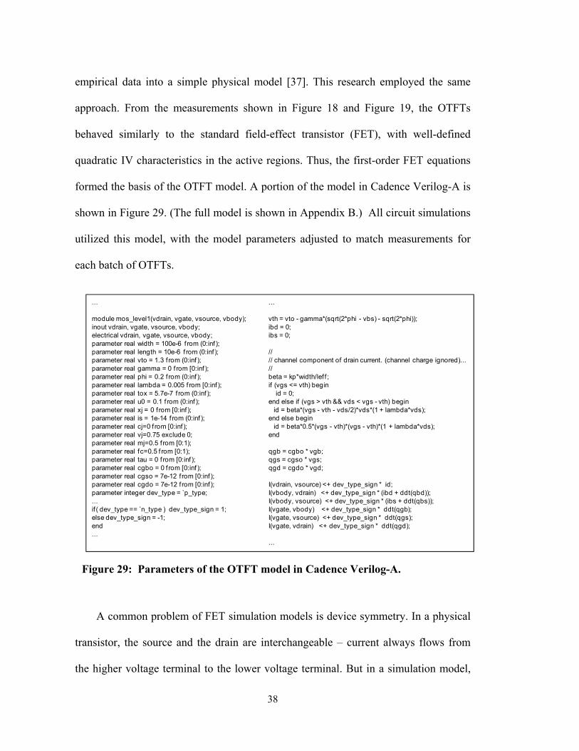
38
empirical data into a simple physical model [37]. This research employed the same
approach. From the measurements shown in Figure 18 and Figure 19, the OTFTs
behaved similarly to the standard field-effect transistor (FET), with well-defined
quadratic IV characteristics in the active regions. Thus, the first-order FET equations
formed the basis of the OTFT model. A portion of the model in Cadence Verilog-A is
shown in Figure 29. (The full model is shown in Appendix B.) All circuit simulations
utilized this model, with the model parameters adjusted to match measurements for
each batch of OTFTs.
A common problem of FET simulation models is device symmetry. In a physical
transistor, the source and the drain are interchangeable – current always flows from
the higher voltage terminal to the lower voltage terminal. But in a simulation model,
Figure 29: Parameters of the OTFT model in Cadence Verilog-A.
...
module mos_level1(vdrain, vgate, vsource, vbody);inout vdrain, vgate, vsource, vbody;electrical vdrain, vgate, vsource, vbody;parameter real width = 100e-6 f rom (0:inf );parameter real length = 10e-6 f rom (0:inf );parameter real vto = 1.3 f rom (0:inf );parameter real gamma = 0 f rom [0:inf );parameter real phi = 0.2 f rom (0:inf );parameter real lambda = 0.005 f rom [0:inf );parameter real tox = 5.7e-7 f rom (0:inf );parameter real u0 = 0.1 f rom (0:inf );parameter real xj = 0 f rom [0:inf );parameter real is = 1e-14 f rom (0:inf );parameter real cj=0 f rom [0:inf );parameter real vj=0.75 exclude 0;parameter real mj=0.5 f rom [0:1);parameter real fc=0.5 f rom [0:1);parameter real tau = 0 f rom [0:inf );parameter real cgbo = 0 f rom [0:inf );parameter real cgso = 7e-12 f rom [0:inf );parameter real cgdo = 7e-12 f rom [0:inf );parameter integer dev_type = ̀ p_type;...if ( dev_type == ̀ n_type ) dev_type_sign = 1;else dev_type_sign = -1;end...
...
vth = vto - gamma*(sqrt(2*phi - vbs) - sqrt(2*phi));ibd = 0;ibs = 0;
//// channel component of drain current. (channel charge ignored)...//beta = kp*width/lef f ;if (vgs <= vth) begin
id = 0;end else if (vgs > vth && vds < vgs - vth) begin
id = beta*(vgs - vth - vds/2)*vds*(1 + lambda*vds); end else begin
id = beta*0.5*(vgs - vth)*(vgs - vth)*(1 + lambda*vds);end
qgb = cgbo * vgb;qgs = cgso * vgs;qgd = cgdo * vgd;
I(vdrain, vsource) <+ dev_type_sign * id;I(vbody, vdrain) <+ dev_type_sign * (ibd + ddt(qbd));I(vbody, vsource) <+ dev_type_sign * (ibs + ddt(qbs));I(vgate, vbody) <+ dev_type_sign * ddt(qgb);I(vgate, vsource) <+ dev_type_sign * ddt(qgs);I(vgate, vdrain) <+ dev_type_sign * ddt(qgd);
...

39
the terminals are predefined as “source” or “drain”, and the current flows in a
predefined direction, which fails to reflect the physical interchangeability of the
terminals. For the OTFT model developed for this research, ideal diodes formed an
alternative route for the current to flow “backward”, allowing the interchangeability of
the terminals. Figure 30 shows a schematic of this OTFT model. Also shown in Figure
30 is the capacitor model. The capacitor model contained two non-ideal diodes to
simulate the effect of dielectric leakage. The diode’s IV characteristics matched the
result from (3.5). Symmetry required the use of two diodes in the capacitor model.
Despite using measurement data in the simulation models, large discrepancies
often existed between OTFT performances and the model predications. The OTFT
variations were too great to allow for accurate modeling. Accordingly, the models
could only provide a “ball-park” estimate of the circuit behavior. The circuit design
needed to be sufficiently flexible to tolerate large imprecision.
Figure 30: Schematics of the OTFT model (left); The capacitor model (right).

40
4. Design of Organic DAC and ADC
Data converters are ideal demonstrations of the research goals stated in Chapter 1.
Any system that connects an analog signal transducer, such as an antenna, an actuator,
a sensor, or a display, to a digital signal processor requires data converters. Moreover,
the main attributes of data converters – linearity, speed and power – are fundamental
to all analog circuits. By implementing data converters with organic transistors, this
research attempted to build a design framework that can apply to other analog circuits.
In a data converter, the most fundamental requirements are resolution and conversion
rate. Resolution is largely a measure of circuit linearity, in particular, how well the
circuit elements are matched along the transfer characteristic. Conversion rate depends
on the operating speed of the circuit, specifically, how quickly the circuit elements can
settle to their steady-state so a conversion decision can be made. (This assumes the
data converter is not the type that utilizes incomplete settling to achieve a conversion
rate higher than indicated by the steady-state settling time.) In this research, the data
converter designs primarily focused on the resolution and the conversion speed. The
designs also considered power consumption, but not as a main focus.

41
4.1. Design Limitations due to the OTFT Process
The poor characteristics of the OTFT processing detailed in Chapter 3 – device
mismatch, large parasitic capacitances, dielectric leakage, and modeling inaccuracies –
limited the available design space of the data converters. Device mismatch introduced
nonlinearity, thus limiting the effective resolution of the data converter. Large
parasitic capacitances slowed circuit settling time, reducing the maximum operating
speed of the data converter. Dielectric leakage created voltage errors during sample-
and-hold, preventing the data converter from operating slowly and removing the
option of exchanging speed for accuracy. Finally, the modeling inaccuracies added
uncertainty to the design – a good-performing circuit in simulation might translate into
a non-functional circuit in reality, or a barely-working one with unacceptably poor
yield. These limitations can be visualized in Figure 31. For example, in a silicon
CMOS data converter, the available design space might be bounded by the larger
dotted lines. In the OTFT process, the aforementioned process characteristics served to
compress the available design space to the much smaller box. Indeed, the negative
impacts of these process characteristics might be so severe as to completely void the
design space, making a functional data converter impossible. Previous attempts at
organic data converters were unsuccessful (V. Subramanian, personal communication)
possibly due to similar constraints in their OTFT processes. This research was
successful in creating the world’s first organic data converters through improvements
in the fabrication process, careful analyses of process constraints, and devising
techniques to overcome each of these constraints.

42
Figure 32: Current-steering DAC (top) and switched-capacitor DAC (bottom) architectures.
b0 b1 b2 bn-2 bn-1
IOUT
VDD
Iu 2Iu 4Iu 2n-2Iu 2n-1Iu
VREF
VOUTCu Cu 2Cu 4Cu 2n-2 Cu 2n-1 Cu
bn bn-1 bn-2 b2 b1
Cp
Figure 31: OTFT process characteristics limit the available design space.
resolution
speed
yield
Modelinaccuracy
Device mismatch
Largecapacitances
Dielectricleakage
resolution
speed
yield
Modelinaccuracy
Device mismatch
Largecapacitances
Dielectricleakage

43
4.2. DAC Design and Measurement
4.2.1 DAC Architecture
Numerous DAC architectures exist, including current-steering and switched-
capacitor types, shown in Figure 32. For a current-steering DAC, the critical parameter
is the matching of the drain currents between the elemental transistors that make up
the array. For a B-bit binary-weighted DAC, the maximum allowed current mismatch
can be calculated using the following expressions [49]:
( )( )YerfinvINL
INL2
=σ (4.1)
( )( )YerfinvDNL
DNL2
=σ (4.2)
BINL
INLu2
2_
σσ ≈ (4.3)
12_
−≈
BDNL
DNLuσσ (4.4)
where erfinv is the inverse error function, and σu_INL and σu_DNL represent the standard
deviations (σ) of the transistor-current mismatches, respectively. With B = 6, INL < 1
LSB, DNL < 1 LSB and Y = 0.95 (corresponding to a confidence interval of 2 sigma),
the DAC requires σu_INL < 12.7% and σu_DNL < 6.4%. However, as described in
Chapter 3, the use of shadow masks and non-uniformities in OTFT mobility
introduced transistor mismatches far greater than 6.4%. From Figure 23, measurement

44
of 60 p-type and 60 n-type OTFTs on one substrate showed 1-σ drain-current
mismatches of 39% and 23%, respectively. Because of these large variations, the
current-steering architecture was not suitable for our OTFT process.
In a switched-capacitor DAC, because the transistors function as switches, the
precision of their currents had little impact on the output. Rather, the critical parameter
was the matching between the capacitors in the array. Although the capacitors also
have mismatches due to the OTFT processing, their precision was far higher than that
of transistor currents because of the capacitor’s simple square geometry. As shown in
Figure 25, measurement of 120 capacitors showed 1-σ capacitance mismatches of
8.4% for 0.0025 mm2 capacitors (17.5 pF), 4.7% for 0.01 mm2 capacitors (70 pF) and
1.7% for 0.04 mm2 capacitors (280 pF). Moreover, the mismatch followed
approximately the area-scaling rule of (3.1). This result illustrated that this OTFT
process exhibited a similar characteristic as that of typical silicon CMOS process – the
mismatch between capacitors could be reduced by increasing their areas.
For a 6-bit switched-capacitor DAC, a requirement of less than 1-LSB INL and 1-
LSB DNL, and 95% yield, the maximum mismatch of binary-weighted capacitors can
also be calculated using (4.1) – (4.4), giving σu_INL < 12.7% and σu_DNL < 6.4%. For a
6.4% mismatch, 0.01 mm2 unit capacitors were chosen, with a unit capacitance of 70
pF. However, in a binary-weighted DAC, the largest capacitance was 2(B-1) times the
unit capacitance, equaled to 2240 pF for 6 bits. This large capacitance, together with
the relatively high on-resistances of the OTFTs, resulted in a long DAC settling time
and low operating speed. An alternative DAC architecture was thus needed to reduce

45
the capacitance – leading to the C-2C design. In a C-2C DAC, at any node in the
circuit the largest capacitance is no more than twice that of the unit capacitor and thus
significantly reducing the settling time. Furthermore, a 6-bit binary-weighted DAC
required 64 unit capacitors – a large amount that was difficult to fabricate with high
process yield at this nascent stage of process development. A 6-bit C-2C DAC
required only 17 unit capacitors – a quantity easier to achieve high process yield.
Figure 33: C-2C structure on silicon suffers from parasitic substrate capacitances (top); The same C-2C structure on glass or plastic has no substrate capacitance (bottom).
Cu Cu 2Cu Cu 2Cu Cu 2Cu Cu 2Cu
Conductive silicon substrate
Cp Cp
Cu Cu 2Cu Cu 2Cu Cu 2Cu Cu 2Cu
Conductive silicon substrate
Cp Cp
Conductive silicon substrate
Cp CpCp Cp
Cu Cu 2Cu Cu 2Cu Cu 2Cu Cu 2Cu
Glass or plastic substrate
Cp CpXXCu Cu 2Cu Cu 2Cu Cu 2Cu Cu 2Cu
Glass or plastic substrate
Cp CpXXCp CpCp CpXX

46
In the silicon CMOS process, the C-2C topology suffered from parasitic
capacitances between the summing nodes and the silicon substrate [50]. The parasitic
capacitances could be as much as 30% of the unit capacitance of the C-2C array. But
with the organic process, the substrate was insulating glass or plastic and did not
contribute to parasitic capacitances, as illustrated in Figure 33.
A schematic of the C-2C DAC is shown in Figure 34: S1 and S2 are the pull-up
and pull-down switches, respectively; S3 is a complementary transmission gate for
sampling a reset voltage VRESET (the need to sample VRESET is described in Section
4.2.3 on combating dielectric leakage). Since the capacitor network is linear,
superposition can be applied to calculate the DAC output voltage VOUT :
∑−
=
−−
++
+=
1
0
)(2B
i
iBiREF
LOADOUT
OUTRESET
LOADOUT
LOADOUT bV
CCC
VCC
CV (4.6)
Figure 34: Circuit schematic of the C-2C DAC; VREF = 3 V, VRESET = 1.5 V.
2C
VRESET
VOUT
VRESETVREFVREFVREF
2C CCCC
C/64 C/64C/64
...
...
VREF
off-chip calibration
Bit 0 (LSB) Bit 1 Bit 5 (MSB)Bit 2, 3, 4
S1 S2
S3
CLOAD

47
COUT is the equivalent output capacitance of the DAC, equaling to 2Cu, where Cu is the
capacitance of one unit capacitor. CLOAD is the load capacitance at the DAC output,
equaling to approximately 4Cu in this design. B is the number of bits, and bi is the ith
bit, either 1 or 0. VREF equals 3 V, and VRESET equals 1.5 V.
Calculation of the DNL of the C-2C DAC gives the appropriate unit-capacitor
size. The DNL at the major code transitions determines the matching requirement at a
given yield. Similar to a binary-weighted DAC, the maximum DNL of the C-2C DAC
occurs at the mid-code transition – i.e. from 011111 to 100000. Analysis of the C-2C
network shows that the maximum allowed unit-capacitor mismatch can be calculated
from the following expressions:
BDNLuDNL
22_
2 241 σσ ≈ (4.7)
( )( )YerfinvDNLB
DNLuDNL2
221
_ =≈ σσ (4.8)
where σDNL is the standard deviation of the DNL at the mid-code transition and σu_DNL
is the standard deviation of the unit-capacitor mismatch. For B = 6, DNL < 1 LSB and
a yield of 95%, σu_DNL = 1.6%, a much more stringent requirement than that for a
binary-weighted DAC. This need for better matching in a C-2C DAC is the result of
having a lower output capacitance – instead of spreading the DNL over 2B times the
unit capacitance as in a binary-weighted DAC, the C-2C DAC can only spread the
DNL over 2 times the unit capacitance. Comparing (4.4) and (4.8), a C-2C DAC
requires a unit-capacitor matching that is approximately square-root(2B-1) times better

48
than that of the binary-weighted DAC. To achieve 1.6% matching, 0.04 mm2 unit
capacitors were chosen with a unit capacitance of 280 pF. Figure 35 illustrates the
relationships between the number of bits, the unit capacitor matching σu_DNL, and the
unit capacitances for C-2C and binary-weighted DACs. Compared to a binary-
weighted DAC, although the unit-capacitor size of a C-2C DAC was larger, the
capacitance needing to be switched at the MSB node was significantly smaller: 280 pF
for C-2C versus 2240 pF for binary-weighted (32 x 70 pF). This reduced switching
Figure 35: Comparison of the unit capacitor matching (σu_DNL) and the corresponding unit capacitance required for C-2C and binary-weighted DACs in our organic process (for DNL = 1, yield = 95%).
1
10
100
1000
10000
100000
1000000
0.01
0.1
1
10
100
2 4 6 8 10 12
Uni
t Cap
acita
nce
(pF)
σ u_D
NL
(%)
Number of Bits
C-2C
C-2C
BW
BW

49
capacitance resulted in a faster DAC speed. In terms of the total capacitance in the
DAC, the C-2C contained 4760 pF, whereas the binary-weighted contains 4410 pF.
Thus, the C-2C DAC was only slightly larger in capacitor area than the binary-
weighted DAC.
4.2.2 Calibration
To correct any realistic deviations from analysis and process parameters, a two-
bit calibration circuit was added externally at the output of the C-2C DAC, shown in
Figure 34. The calibration circuit consisted of three thermometer-coded elements, each
represented by a 4.7 pF capacitor that was approximately 1/64th of the C-2C unit
capacitor. Although the calibration was implemented off-chip with discrete CMOS
switches and discrete capacitors, the concept could be readily fabricated on-chip: the
smallest individual capacitor that could be fabricated in this organic thin-film process
was 2.8 pF (limited by the minimum opening in the shadow masks); and thermometer
coding guarantees monotonicity despite any large mismatches between the small
calibration capacitors. A similar calibration circuit was implemented on-chip when the
DAC was integrated as a part of the ADC.
4.2.3 Limits on DAC Operating Speed
Section 3.2 discussed the maximum operating speed in the context of the
transistor transit frequency fT. For the DAC, the settling time of the output voltage

50
limits the maximum operating speed. For the C-2C DAC, the settling at the output
node is approximately equal to the settling of the MSB node because any settling
errors at lower bits will be attenuated by the C-2C network. The time ts required to
settle to within 1 LSB of a B-bit DAC can be calculated using the following
expression:
( ) TOTALONs CRBt 2ln= (4.12)
where RON is the on-resistance of the p-type or the n-type OTFT switch at the MSB
node (S1 or S2 in Figure 34) and CTOTAL is the total load capacitance to this OTFT.
RON can be calculated from the following expression:
( )( )THGSOXON VVLWC
R−
=μ
1 (4.13)
With the device parameters specified in Section 3.2, to obtain equal RON, the width of
the n-type OTFT (Wn) needed to be ten times the width of the p-type OTFT (Wp). As a
reasonable compromise that avoids excessively large devices, the DAC used Wn =
5Wp. With Wp = 200 μm, Wn = 1000 μm, and VGS = 3 V, the approximate on-
resistances were 714 kΩ and 1428 kΩ, for the p-type and n-type OTFTs, respectively.
CTOTAL in (4.11) equaled approximately 620 pF (the sum of CU = 280 pF and all
overlap capacitances at the OTFT drain node equaling approximately 340 pF). Thus,
the maximum operational speed of the 6-bit DAC was 1/(2ts) ≈ 132 Hz. (Although the
overlap capacitances of the OTFT switches were substantial, because they were not
connected to the charge conservation nodes between the C and 2C capacitors, they did
not affect the 1:2 ratio required for the C-2C operation.)

51
A lower limit on the operational speed was governed by the dielectric leakage
current through the capacitors. In this organic thin-film process, the leakage current
through a capacitor was nonlinearly related to the applied capacitor voltage (see
Figure 27), resulting in input-dependent output errors. The slower the operation and
the longer the capacitors lost charge through leakages, the greater the errors. Section
3.3 described the leakage measurement and the derived leakage model. To quantify
the amount of errors and thus establish a lower bound on the operating speed, the
change in the DAC output voltage is calculated as a function of the leakage current
and the DAC clock rate. At the DAC output, the error in the output voltage is a
weighted function of all capacitor leakages. Calculating the exact worst case value of
the error is analytically difficult. However, the calculation can be simplified by
recognizing that the MSB capacitor leakage holds the greatest contribution to the
output voltage error, since the C-2C network attenuates the effects of all other
capacitor leakages. Therefore, only considering the MSB capacitor allows a simple
estimate for the minimum frequency fmin of the DAC:
OUT
LEAK
VCI
tf
Δ=
Δ=
2
21
min (4.16)
ε
Ba
V
U
CeI
Cf 21
21
0min ⎟⎟⎠
⎞⎜⎜⎝
⎛−= (4.17)
where ε is the allowed output error due to leakage. Although this result is a simplified
estimate, it offers insight into the relationship between the minimum speed limit of the
DAC and its dependencies. For CU = 280 pF, VC = 1.5 V and ε = 1 LSB, Figure 36

52
plots fmin as a function of the leakage coefficient a. In the empirical leakage model
developed in Section 3.3, a = 0.45 V; thus the minimum operating frequency of this 6-
bit DAC is estimated to be 1.8 Hz. This minimum frequency is small because the full-
scale range of the DAC output was purposefully designed such that the maximum Vc
was 1.5 V. At Vc = 2.5 V, the leakage would have been ten times greater, and thus the
minimum frequency would be a more detrimental 18 Hz. Further, variations in I0 or
the leakage coefficient a (due to temperature or process) could significantly alter this
minimum frequency, as shown in Figure 36. To prevent leakage errors from
accumulating over multiple clock cycles, the DAC recharges all capacitors by
sampling VRESET every clock cycle, as shown in Figure 34.
Figure 36: Minimum DAC frequency required for 1-LSB output error due to capacitor leakage (8-bit and 10-bit are included for comparison).
0.3 0.35 0.4 0.45 0.5 0.55 0.610
0
101
102
Leakage coefficient (V)
Min
imum
freq
uenc
y (H
z)
B = 6B = 8B = 10

53
4.2.4 DAC Measurement
The DAC was fabricated on a commercial LCD glass substrate measuring 88 mm
× 88 mm. The glass was placed in the probe station for measurement. Two custom-
designed multi-probe handlers (MPHs) provided the interface contacts. Wire bonding
was attempted but was unsuccessful due to insufficient adhesion between the gold
pads and the glass surface. The MPHs were connected to the FPGA board via an
adapter board. The FPGA provided the digital signals to the DAC. All signals were
loaded with appropriate capacitances on the adapter board to reflect realistic OTFT
conditions. The DAC output was connected to an oscilloscope. All measurements
were performed in ambient air and at room temperature. Appendix A includes detailed
descriptions of the test platform.
The DAC contained twelve capacitors – seven 280 pF unit capacitors, and five 560
pF capacitors each formed from two unit capacitors. To increase the sample size, two
DACs were measured. (One capacitor was damaged during measurement for a total
sample size of 23.) The standard deviation of the unit capacitor mismatches was
3.4%, twice as much as that of the test capacitors in Section 3.1. There were two
possibilities for the wider distribution: 1. in the actual circuit, the shadow mask
openings for capacitors were more difficult to control due to adjacent circuitry; 2. the
dielectric thickness might vary across the circuit. The mismatch standard deviation of
the 560 pF capacitors was 2.1%, equaled to 0.62 of the mismatch standard deviation of
the 280 pF capacitors, approximately conforming to the area-scaling rule (square root
of 280/560 = 0.707).

54
Figure 38: Measured DAC output voltage error (code 63, before calibration) as a function of the clock rate; from top to bottom: 0.1 Hz, 0.5 Hz, 1 Hz, 2 Hz, 5 Hz and 10 Hz.
0.1 0.2 0.3 0.4 0.5-1
0
1
2
3
4
Clock period (TCLK)
DA
C o
utpu
t vol
tage
err
or (L
SB)
Figure 37: Measured DAC transfer function (before calibration) becomes increasingly nonlinear as the clock rate increases from 100 Hz to 500 Hz.
0 16 32 48 631
1.2
1.4
1.6
1.8
2
2.2
Input code
Out
put v
olta
ge (V
)
100 Hz200 Hz300 Hz400 Hz500 Hz

55
Figure 37 and Figure 38 illustrate the upper and the lower speed limits of the
DAC. In Figure 37, as the clock rate increased above 100 Hz, the measured
(uncalibrated) DAC transfer function became increasingly distorted, as predicted by
(4.12) – (4.13). In Figure 38, as the clock rate decreased below 10 Hz, the leakage
error progressively worsened. At 2 Hz, the leakage error was 0.5 LSB, approximating
the 1 LSB error predicted by (4.14) – (4.17).
Figure 39 shows the measured DAC transfer function after calibration, together
with the ideal characteristic described by (4.6). Compared to the ideal transfer
function, the measured transfer function had a 60 mV offset and an 8% gain error. The
offset was due to the residual voltage from the calibration circuit; and the gain error
resulted from the imprecise estimation of CLOAD. Figure 40 shows the static linearity
of the DAC, as measured by DNL and INL at a conversion rate of 100 Hz. Before
Figure 39: Ideal and measured (after calibration) DAC transfer functions at 100 Hz conversion rate.
0 16 32 48 631
1.2
1.4
1.6
1.8
2
2.2
Input code
Out
put v
olta
ge (V
)
MeasuredIdeal

56
calibration, the maximum DNL and INL were -2.8 LSB and +3.1 LSB, respectively.
After calibration, the maximum DNL and INL were -0.6 LSB and -0.8 LSB,
respectively. Figure 41 shows the spectrum of two output sinusoids at 10 Hz and 45
Hz, synthesized at the conversion rate of 100 Hz. The harmonic spurs of the sinusoids
are clearly visible. For the 10 Hz output, the highest spur was at -24 dBc. For the 45
Hz output, the highest spur was at -29 dBc. For sinusoids between 1 Hz to 49 Hz, the
worst case occurred at 10 Hz. Thus, the spurious-free dynamic range (SFDR) of the
DAC was 24 dB.
Figure 40: DAC DNL and INL before calibration [(a) and (b)] and after calibration [(c) and (d)].
0 16 32 48 63-1
-0.5
0
0.5
1
Input code
DN
L (L
SB)
0 16 32 48 63-1
-0.5
0
0.5
1
Input code
INL
(LSB
)
0 16 32 48 63-4
-3
-2
-1
0
1
2
3
4
Input code
INL
(LSB
)
0 16 32 48 63-4
-3
-2
-1
0
1
2
3
4
Input code
DN
L (L
SB)
(a) (b)
(c) (d)

57
A photograph of the DAC is shown in Figure 42. (The substrate sits on a black
background to enhance visibility.) The circuit contained thirteen p-type OTFTs,
thirteen n-type OTFTs, and seventeen unit capacitors. The total area of the DAC was
28 mm × 14 mm.
Figure 41: Spectrum of 10 Hz and 45 Hz DAC output sinusoids (500-point FFT).
0 10 20 30 40 50-60
-40
-20
0
Frequency (Hz)
Am
plitu
de (d
Bc)
0 10 20 30 40 50-60
-40
-20
0
Frequency (Hz)
Am
plitu
de (d
Bc)

58
4.3. ADC Design and Measurement
4.3.1 ADC Architecture
In Section 3.1, measured mismatch distributions showed that capacitors could be
made an order of magnitude more precisely than OTFTs. Moreover, capacitor areas
could be scaled to achieve a desired matching precision. These process characteristics
were applied to the design of the switched-capacitor C-2C DAC. Similarly, the
successive approximation register (SAR) architecture was chosen for the ADC
because the conversion accuracy of a SAR ADC largely depends on capacitor
matching [49]. The OTFTs in the SAR ADC act as on-off switches and have minimum
Figure 42: Photograph of the C-2C DAC on glass substrate.
2 mm

59
effect on the conversion accuracy once the circuit has settled.
For the design target of 6-bit conversion, a SAR ADC requires 6 cycles to reach
each valid output; however, as most organic applications deal with relatively static
signals – such as an organic sensor that detects chemical reactions, high speed was not
a requirement for this OTFT data converter: a 10 Hz conversion rate was deemed
sufficient. (Conversely, the speed could not be too slow as to result in large errors due
to dielectric leakage.) As shown in Figure 43, the SAR ADC contained four main
blocks – the C-2C DAC from Section 4.2, the calibration DAC, the comparator, and
the digital SAR logic. Because the primary goal of this research was to validate
organic analog circuits, the digital SAR logic was implemented in an external field-
programmable gate array (FPGA) board. All interfaces between the FPGA board and
the organic circuits were loaded with appropriate capacitances and resistances to
reflect realistic OTFT parasitics.
Figure 43: SAR ADC, showing its main circuit blocks.
Organic ProcessOrganic Process

60
Of the four process limitations described in Chapter 3, two had been mitigated
through architectural selections: the switched-capacitor topology in the DAC and the
SAR topology in the ADC circumvented the poor matching of the OTFTs; the C-2C
topology of the DAC improved the conversion rate despite the large parasitic
capacitances. Moreover, the parasitic capacitances – more precisely the variations in
the parasitic charges from the OTFT switches, did not affect the sample-and-hold
accuracy because the C-2C structure uses bottom-plate sampling [49]. The “true”
sampling switch is the OTFT connected to VMID in Figure 44. Although it also injects
parasitic charges, those charges are constant for all ADC voltages in the absence of
hysteresis. (Chapter 2 showed that the OTFTs had negligible hysteresis.)
In the DAC, resetting the capacitor to a voltage VRESET every clock cycle
prevented the dielectric leakage charges from accumulating over multiple clock
cycles. In the ADC, a set of input sampling switches were integrated within the C-2C
structure, as shown conceptually in Figure 43 and schematically in Figure 44. To
prevent the accumulation of dielectric leakage charges, the ADC sampled the input
every clock cycle, rather than every sixth clock cycle as in a typical 6 bit SAR ADC.
Re-sampling every clock cycle effectively resets the capacitors in the C-2C array, but
results in tracking errors if the rate of change of the input exceeded 1/6 least-
significant-bit (LSB) per clock period, equivalent to 530 mV/sec at the 100 Hz clock
rate in this ADC design. For slow-changing signals, such as that from our intended
chemical sensor, this re-sampling technique does not introduce appreciable tracking
error.
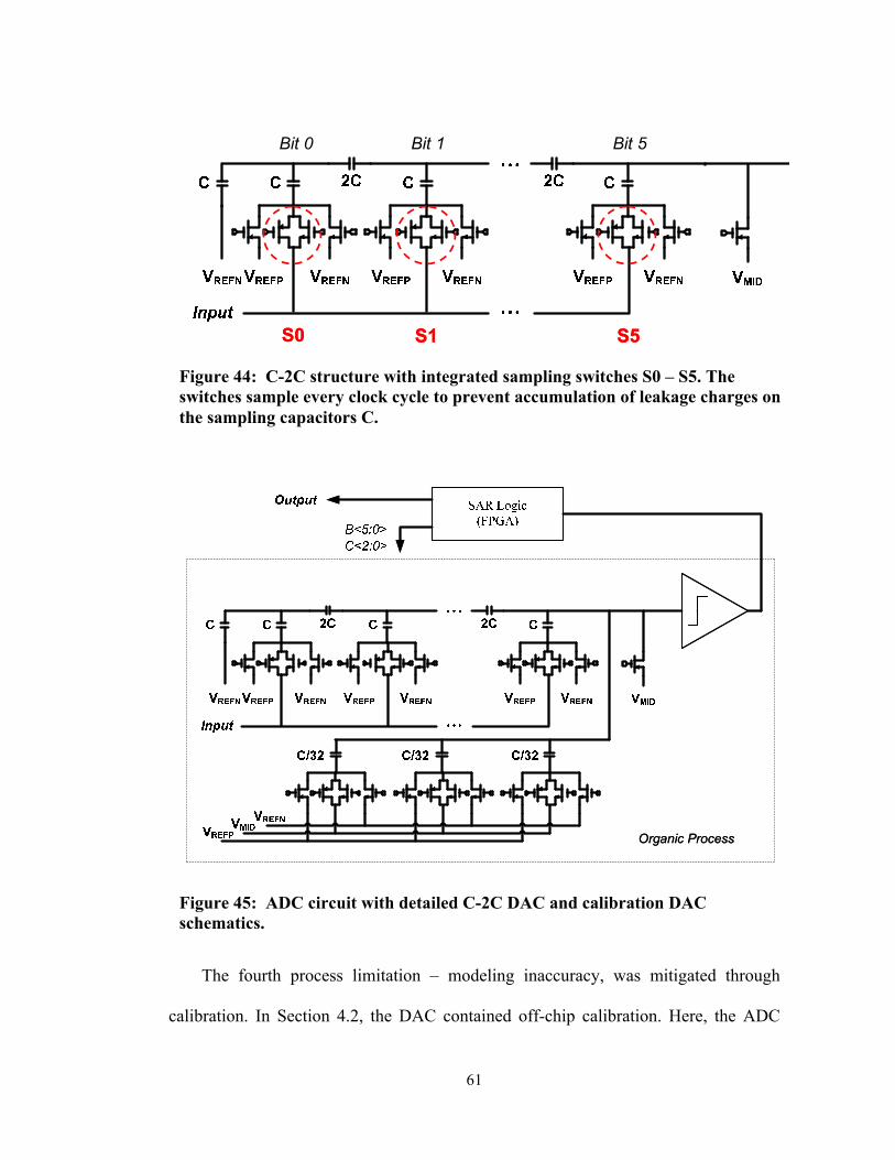
61
The fourth process limitation – modeling inaccuracy, was mitigated through
calibration. In Section 4.2, the DAC contained off-chip calibration. Here, the ADC
Figure 45: ADC circuit with detailed C-2C DAC and calibration DAC schematics.
Organic ProcessOrganic Process
Figure 44: C-2C structure with integrated sampling switches S0 – S5. The switches sample every clock cycle to prevent accumulation of leakage charges on the sampling capacitors C.
Bit 0 Bit 1 Bit 5
S0 S1 S5
Bit 0 Bit 1 Bit 5
S0 S1 S5

62
implemented on-chip calibration using a two-bit thermometer-coded calibration DAC.
The calibration DAC corrected any realistic deviations from the simulation model.
Figure 45 shows the circuit schematics of the C-2C DAC with the integrated sampler
and the calibration DAC. The calibration DAC used the same basic OTFT design as
the C-2C DAC, but with 8.75 pF unit capacitors formed from connecting multiple 280
pF capacitors in series. In the design of the calibration DAC, layout became a
particular concern. The calibration DAC required 12 control signals. Due to test
platform limitations, these additional control signals forced multiple voltage lines,
such as VREFP, VREFN, VMID, to be combined in layout, resulting in 60 signal
crossovers. Because the dielectric was only 5.7 nm thick, any crossover would lead to
large parasitic capacitance, or potential shorts. By only allowing crossovers between
constant-voltage lines and digital control lines, the circuit avoided the deleterious
effects of parasitic capacitances. To prevent shorts, additional layout spaces were
inserted between traces in the vicinity of the crossovers. Figure 46 shows a photograph
of the ADC on the glass substrate.

63
4.3.2 Auto-zeroed Comparator Design
The comparator formed the decision-making part of the ADC. Figure 47 shows
the circuit schematic of the comparator. Several design considerations led to the use of
inverter-based gain stages: 1. The comparator must tolerate large device mismatches;
2. The comparator must self-bias to avoid the variability of biasing circuitry; 3. To
avoid poor yield, the comparator should be simple. The cascade of inverter-based gain
stages satisfied all these conditions. In particular, the inverter was robust against the
effects of OTFT mismatch because it could automatically self-bias to a high-gain dc
Figure 46: Photograph of the ADC on the glass substrate.
C-2C DAC
C-2C DAC
Cal DAC
CompC-2C DAC
C-2C DAC
Cal DAC
Comp

64
operating point. By introducing a two-phase operation, as illustrated in Figure 48, any
static offset in the inverter, such as threshold voltage drift, was zeroed as the offset is
common to both phases. In the reset phase, the transmission gate shorted the input to
the output, establishing the dc operating point, and fixing the bottom plate of CS1 to
this dc voltage (VDC). Simultaneously, the DAC charged the top plate of CS1 to a
voltage proportional to the DAC code (VDAC). In the sample-compare phase, the
transmission gate shuts off. The DAC then switched to the sampling mode. The
voltage on the top plate of CS1 was now proportional to the input (VIN); and the
voltage on the bottom plate of CS1 was now proportional to (VDC + VIN – VDAC). The
difference (VIN – VDAC) was then amplified by the inverter, thus obtaining a
Figure 47: The comparator circuit and device parameters.

65
comparison between the DAC code and the sampled input.
The comparator gain AV could be calculated from the expression below [49]:
BFSR
DCOUTV V
VVA −⋅⋅
−=
2ε (4.18)
where VOUT – VDC is the change in the output voltage between the reset and the
sample-compare phases, ε is the desired output accuracy, VFSR is the input full-scale
range (FSR), and B is the number of bits. For this ADC, VOUT = 0 or 3 V, VDC = 1.5 V,
ε = 0.5 LSB, VFSR = 2 V, and B = 6 bits, the comparator required a gain of 96. To
achieve 100 Hz clock rate, the comparator needed to settle within 5 ms (half of one
clock cycle).
A gain of 96 with a settling time of 5ms was beyond the state-of-art in organic
circuits [37]. Conventional linear amplifier designs could not reach this target in
Figure 48: Two-phase operation of the comparator.
Reset phase
VOUT = A(Vin – VDAC)
Sample phase
VC+ = VDAC VC
- = VDC
VC+ = Vin VC
- = VDC + Vin - VDAC
Reset phase
VOUT = A(Vin – VDAC)VOUT = A(Vin – VDAC)
Sample phaseSample phase
VC+ = VDAC VC
- = VDC
VC+ = Vin VC
- = VDC + Vin - VDAC

66
organic technology. However, inverters could provide suitably high gain, but in a
narrow voltage range, as demonstrated by the measured transfer function of an OTFT
inverter in Figure 49. The maximum small-signal gain of the inverter was in excess of
60. In the comparator, the two-phase operation conveniently acted as the self-biasing
mechanism for the inverter and automatically placed the quiescent point within the
high-gain voltage range. Moreover, the ultra-thin dielectric and the SAM passivation
effectively suppressed bias-induced hysteresis, allowing inverters to be used without
suffering from metastability.
In the comparator, a cascade structure was chosen over a regenerative latch.
Countering process variations required that each inverter to be individually self-
biased. In a latch, such requirement forced ac-coupling of the feed-forward and the
feedback paths, resulting in lowered gain from the additional capacitive load. In a
cascade, analysis showed that the ac-coupled inverter (such as the one shown in Figure
51) gain Astep(t) in response to an input step is
Figure 49: Measured transfer function (left) and small-signal gain (right) of an OTFT inverter, with Wp = Wn = 500 μm, Lp = Ln = 20 μm.
0
1
2
3
0 1 2 3
Vout
(V)
Vin (V)
-80
-60
-40
-20
00 1 2 3
smal
l-sig
nal g
ain
(V/V
)
Vin (V)
0
1
2
3
0 1 2 3
Vout
(V)
Vin (V)
-80
-60
-40
-20
00 1 2 3
smal
l-sig
nal g
ain
(V/V
)
Vin (V)

67
mnmpmFloadL
gdngdpF
gsngspSF
F
F
S
L
m
L
Fstep
ggGCCC
CCC
CCCCC
CC
A
tCG
CC
AtA
+=−+=
+=
+++=−=
⎟⎟⎠
⎞⎜⎜⎝
⎛⎟⎟⎠
⎞⎜⎜⎝
⎛−⎟⎟
⎠
⎞⎜⎜⎝
⎛+−=
,)1(
where
exp11)(
0
0
β
β
ββ
(4.19)
And the time constant τ is
m
L
GC
βτ = (4.20)
The time ts to settle to 95% of the steady-state gain equals approximately 3τ. CS and
CF are the input capacitance and the feedback capacitance of the inverter, respectively,
as shown in Figure 47. Cgs and Cgd are the parasitic gate-source and gate-drain
capacitances of the OTFTs. Cload is the load capacitance at the inverter output node,
and gm is the transconductance of OTFT. The steady-state gain A0 is simply the ratio
of CS to CF, with CF equaling the sum of the gate-drain capacitance Cgd of the p-type
OTFT and the n-type OTFT. To minimize CF, the n-type OTFT was made the same
size as the p-type OTFT. This preserved a reasonable steady-state gain despite the low
n-type mobility, at the expense of longer settling time.
Figure 50 shows the measured transient response of the first gain stage of a test
comparator to a VFSR/64 = 32 mV input. When Clock was low, the output voltage
settled to the DC operating point of 1.5 V. After Clock transitioned to high, an input

68
step of -32 mV was applied, the output voltage then settled to 1.75 V, giving a gain A0
of ΔVout/ΔVin = (1.75-1.50)/-0.032 = -7.8. The comparator in this test case had low
OTFT mobility, resulting in a settling time ts of approximately 13 ms. Both the gain
and the settling time of this test comparator were within the expectation from (4.19).
The actual ADC comparator had approximately five times higher OTFT mobility. The
gains and the settling times of each stage of the ADC comparator are listed in Table 4
and summarized in Figure 47.
Figure 50: Measured transient response of the first gain stage of a test comparator, showing a gain of ΔVout/ΔVin = -7.8 and a settling time of 13 ms. The clock rate was 30 Hz.
0.00
0.50
1.00
1.50
2.00
2.50
3.00
-0.10
-0.05
0.00
0.05
0.10
0.15
0.20
0.020 0.025 0.030 0.035 0.040 0.045 0.050
Cloc
k an
d O
utpu
t Vo
ltage
(V)
Inpu
t Vol
tage
(V)
Time (sec)
Vin = -32mVClockVout
A0 = -7.8
ts = 13ms
Clock HighClock Low
ΔVout
ΔVin

69
Table 4: Nominal OTFT parameters, calculated stage gains and settling times of the ADC comparator.
1st Stage 2nd Stage 3rd Stage 4th Stage Unit
Mobility 0.5 0.5 0.5 0.5 cm2/V-sCox 7 7 7 7 fF/um2
Width 500 400 400 100 umLength 20 20 20 20 umOverlap 20 20 20 20 umVgs -1.5 -1.5 -1.5 -1.5 VVTH -0.5 -0.5 -0.5 -0.5 VCgs 70 56 56 14 pFCgd 70 56 56 14 pF
Mobility 0.02 0.02 0.02 0.02 cm2/V-sCox 7 7 7 7 fF/um2
Width 500 400 400 300 umLength 20 20 20 20 umOverlap 20 20 20 20 umVgs 1.5 1.5 1.5 1.5 VVTH 0.5 0.5 0.5 0.5 VCgs 70 56 56 42 pFCgd 70 56 56 42 pF
CS 1100 1100 1100 1100 pFCF 140 112 112 56 pFCload 800 720 720 440 pF
A0 -7.9 -9.8 -9.8 -19.6 V/V
β 0.101 0.085 0.085 0.046CL 926 823 823 493 pFgmp 8.75 7 7 1.75 uSgmn 0.35 0.28 0.28 0.21 uS
time constant 1.00 1.34 1.34 5.45 msec
settling time 3.01 4.01 4.01 16.35 msec
P-ty
pe O
TFT
N-ty
pe O
TFT

70
Although the inverter’s steady-state gain was largely independent of the
inconsistent OTFT transconductance gm, the gain still suffered from variations in Cgd.
To tolerate mask alignment errors during fabrication, large overlaps were created
between the gate metal and the source-drain metals, leading to large Cgd – nominally
70 pF for a 500 μm wide OTFT. Depending on the amount of misalignment, Cgd could
vary from 0 pF to 140 pF over process. To minimize gain variations caused by this
fluctuation in Cgd, the p-type OTFT was placed anti-symmetrical to the n-type OTFT,
as shown in Figure 51. Any increase in Cgd of one OTFT is compensated by an equal
decrease in Cgd of the opposing OTFT, resulting in a constant total Cgd and a constant
gain. (Because CS was a capacitor fabricated from intersecting metal traces, it was
immune to x-y mask misalignment.) Figure 52 shows the cross-sectional views of the
Figure 51: Anti-symmetrical layout of the inverter to maintain constant steady-state gain.
gdngdpF
F
S
CCCCCA
+=
−≈0
P-type OTFT N-type OTFT
gdngdpF
F
S
CCCCCA
+=
−≈0
P-type OTFT N-type OTFT

71
inverter, in the nominal condition and with misalignment.
4.3.3 Digital Logic Implementation
The digital logics resided in the FPGA. The core logic consisted of two main
blocks: the successive-approximation register (SAR) algorithm and the control
interface. Additional blocks included the clock tree, the test mode control, and ROM
to store calibration and test patterns. Calibration was performed off-line in Matlab; and
the resulting correction codes stored in the ROM. All digital logics were written in
Verilog. Chipscope provided the PC interface.
Figure 52: Cross-sectional views of the inverter in the nominal condition (top), with mask misalignment (bottom).
P-type OTFT N-type OTFT
Cgdp Cgdn
P-type OTFT N-type OTFT
Cgdp CgdnCgdp Cgdn
P-type OTFT N-type OTFT
CgdnCgdp
Misalignment
constant 0 ≈−≈F
S
CCA
P-type OTFT N-type OTFT
CgdnCgdp CgdnCgdp
Misalignment
constant 0 ≈−≈F
S
CCA

72
The SAR algorithm was derived from the common binary search routine.
Referring to Figure 43 of the ADC block diagram, at the beginning of the conversion
cycle, the DAC was set to mid-code = 1/2 VDAC/VREF, equivalently 100000 in binary.
If the sampled input was greater than this DAC output, the SAR algorithm
incremented the DAC by 1/4 VDAC/VREF, giving 110000b. Conversely, the SAR
algorithm decremented the DAC by 1/4 VDAC/VREF, giving 010000b. The algorithm
continued until reaching the smallest resolution of 1/64 VDAC/VREF, in a total of six
cycles for a 6-bit algorithm. Figure 53 displays a conceptual diagram of the algorithm.
The state machine shown in Figure 54 represented the binary implementation of the
SAR algorithm in the FPGA.
The control interface managed the 32 signals connecting the FPGA and the
organic circuit – 12 for the C-2C DAC bits, 12 for the calibration DAC, 4 for the
comparator, 2 for the sampling switches, 1 for the reset switch, and 1 for the
comparison output (input to the FPGA).
Figure 53: Conceptual diagram of the SAR algorithm.

73
The timing of some of the main signals is shown in Figure 55. The FPGA could
be timed from an internal fixed-frequency oscillator, or an external clock source. The
external clock allowed variable FPGA frequency, and hence variable ADC sampling
frequency.
Figure 54: State machine of the SAR algorithm implementation. “CMP” is the comparison result between the DAC output and the sampled input, with “1” representing a larger input.

74
4.3.4 ADC Measurement
The ADC was tested in ambient air. Figure 46 shows a photograph of the ADC on
a glass substrate. The ADC included 27 p-type OTFTs, 26 n-type OTFTs, 19
capacitors, 60 crossovers, and over three hundred vias. Total area measured 28 mm x
22 mm. The measured p-type mobility and n-type mobility were 0.5 cm2V-1s-1 and
0.02 cm2V-1s-1, respectively.
Figure 56 shows the measured comparator output as the DAC incremented from
code 17 to 21 while sampling VIN = 1.55 V at 100 Hz. A clear low-to-high transition
Figure 55: Timing diagrams of the main control signals.
DCM50MHz 4MHz
OSC
External4MHz
4MHz /32125KHz FPGA Main Clock
100 phases, 0-100Sample_clk
0
49 0
90 45
61 97
P1e
Set_clk
61 97
cal_clk (if active during output phase)
5 47
cal_reset_clk
94 50
Comp_clk
51 97
resetsw_clkb
DCM50MHz 4MHz
OSC
External4MHz
4MHz /32125KHz FPGA Main Clock
100 phases, 0-100Sample_clk
0
49 0
90 45
61 97
P1e
Set_clk
61 97
cal_clk (if active during output phase)
5 47
cal_reset_clk
94 50
Comp_clk
51 97
resetsw_clkb

75
occurred between code 18 and 19, indicating that the 1.55 V input was converted to
code 19. Figure 57 captures the nonlinearity measurements in the form of the transfer
function of the ADC. The ADC achieved full 6-bit resolution with no missing code at
a sampling frequency of 100 Hz and a conversion rate of 100/6 = 16.7 Hz. The full-
scale range was 1.7 V, slightly lower than the designed 2 V due to the aforementioned
gain error in the DAC (described in Section 4.2). Figure 58 shows the measured
differential nonlinearity (DNL) and integral nonlinearity (INL) of the ADC at the
sampling frequency fs = 100 Hz before calibration. The worst DNL = 2.2 LSB, and the
worst INL = -2.9 LSB. After applying calibration, the worst DNL improved to -0.6
LSB, and the worst INL improved to 0.6 LSB, as shown in Figure 59.
At fs = 100 Hz, the power consumption of the ADC (excluding FPGA) was
simulated to be 3.6 μW, of which the comparator consumed 2.9 μW.
Table 5 summarizes the ADC characteristics; and Table 6 compares this organic
ADC to a recent silicon ADC [51]. This organic ADC achieved higher speed
efficiency (ratio of fs to fT) than the silicon ADC, validating the design methodology of
the organic ADC.

76
Figure 57: Measured ADC transfer function at 100 Hz sampling rate.
0
8
16
24
32
40
48
56
64
1.0 1.5 2.0 2.5 3.0
Out
put C
ode
Input Voltage (V)
Figure 56: Measured comparator output and DAC output, showing that an input voltage had been converted to code 19.

77
Figure 59: Measured ADC DNL and INL with calibration.
0 8 16 24 32 40 48 56 63-1
-0.5
0
0.5
1
DN
L (L
SB)
Code
0 8 16 24 32 40 48 56 63-1
-0.5
0
0.5
1
Code
INL
(LSB
)
Figure 58: Measured ADC DNL and INL without calibration.
0 8 16 24 32 40 48 56 63-4
-2
0
2
4
DN
L (L
SB)
Code
0 8 16 24 32 40 48 56 63-4
-2
0
2
4
Code
INL
(LSB
)

78
Table 6: Comparisons of this organic ADC and a silicon ADC.
Organic SAR ADC(this work)
90 nm Silicon SAR ADC (Draxelmayr, ISSCC 2004)
Resolution 6 bits 6 bits
Sampling rate (fs) 100 Hz 600 MHz
Maximum transistor speed (fT) 18 kHz 150 GHz
Speed efficiency (fs / fT) 5.56 x 10⁻³ 4.0 x 10⁻³
Table 5: Summary of ADC characteristics.
Process 3 metal complementary organic thin-film
Minimum feature size 20 μm
Chip area 28 mm x 22 mm
Resolution 6 bits
Full-scale range 1.7 V
Max DNL / INL -0.6 LSB / 0.6 LSB
Clock rate / Update rate 100 Hz / 16.7 Hz
Power consumption 3.6 μW @ 3 V

79
5. Conclusion and Future Work
5.1. Summary of This Dissertation
Over the past fifty years, silicon semiconductor technology had transformed the
world. The success of silicon-based transistors has created entirely new fields of
electronics and expanded the boundary of imagination. Today, a new class of
applications is emerging – one that adds unconventional dimensions to electronics
with features such as mechanical flexibility, large area at low cost, and integration
with chemistry and biology. Examples include flexible cell phone displays, electronic
paper, printed RFID tags, artificial skin, and biochemical sensors. Organic
semiconductor technology is a promising enabler of these novel applications. Because
organic transistors can be fabricated near room temperature, they allow integrated
circuits to be made on flexible plastic substrates that can bend and flex. The
printability of organic semiconductors can allow transistor to be made in large form-
factors inexpensively. And since most organic semiconductors are inherently sensitive

80
to specific chemical agents, organic transistors make natural chemical and biological
sensors.
As with any nascent technology, numerous difficulties exist in creating integrated
circuits based on organic transistors. The organic transistor fabrication process
presents significant handicaps to circuit design. In this research, we studied the causes
and effects of process handicaps, and devised circuit techniques to overcome them in
the designs of data converters. To achieve acceptable conversion accuracy in the
presence of severe transistor mismatches, we employed switched-capacitor
architecture. To improve conversion speed, we used the C-2C capacitor array rather
than the more conventional binary-weighted array. To prevent dielectric leakage from
introducing errors, we refreshed the capacitors every clock cycle. To mitigate
modeling errors, we added calibration. Finally, to achieve a large voltage gain while
maintaining stable operation under significant process variations, such as variations in
threshold voltage, we designed an auto-zeroing inverter-based comparator. Using
these circuit techniques, along with multiple fabrication and layout considerations, we
built a 3 V, 6-bit organic-transistor DAC and a 3 V, 6-bit organic-transistor ADC. To
our knowledge, these were the first successful data converters in the organic transistor
technology. Although organic transistors are still immature, with careful process-
device-circuit co-design, moderately complex analog organic circuits are within reach.
81
5.2. Future Work
5.2.1 Integration with Organic Sensors
A primary purpose of an ADC is to convert sensory information to digital bit for
digital signal processing. To this end, it is natural to integrate the organic transistor
ADC with organic sensors. The Bao Group in Stanford Chemical Engineering has
developed a number of organic transistor based sensors. One particular sensor has
shown to detect chemical attributes of seawater, including salinity, pH factor, and
concentrations of several amino acids [52]. As this sensor uses FTTF as the
semiconductor, additional fabrication procedures need to be developed to integrate the
sensor with the organic ADC, which uses DNTT and F16CuPc. Secondly, the sensor
operates by immersion in seawater, but exposure to water would destroy the OTFTs in
the ADC. Thus, the ADC needs to be encapsulated in a non-permeable material such
as Parylene. Figure 60 shows a conceptual drawing of the integrated ADC with
organic sensors.
In circuit design, the main issue is the signal interface between the sensor and the
ADC. Since the organic sensor outputs current, whereas this organic ADC reacts to
voltage, a transimpedance amplifier needs to be developed to convert the current to a
voltage. The transimpedance amplifier must use the same types of organic transistor as
the ADC. Based on the existing performances of the organic transistors, a classic
textbook design would unlikely achieve the desired results. New circuit architectures
are needs for the transimpedance amplifier. It is possible that with the improved n-type
OTFT currently under development; the available design space may be expanded

82
sufficiently to allow greater design flexibility beyond switched-capacitors.
A third obstacle to integration is testability. As shown in Appendix A, testing the
organic ADC requires a delicate set of 52 probes. Once integrated, it may be
impossible to immerse the sensor in water while still maintaining probe contact. There
are two solutions to this problem: 1. Move the digital logic on-chip to reduce the
number of probe connections, or 2. Rearrange the probe pads to the peripheral of the
substrate to allow for easier probe connections. Neither solution is straightforward
given the device and process limitations. Substantial efforts should be devoted to solve
the testability problem at the beginning of the project to avoid future dead ends.
5.2.2 Packaging and Physical Interfaces
It is often said that the secret of the semiconductor industry is not the chip design,
Figure 60: The organic ADC integrated with organic sensors.
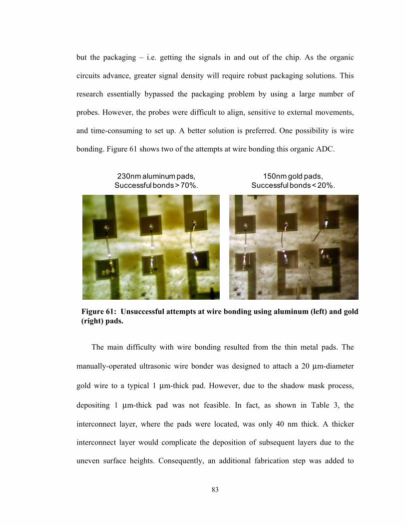
83
but the packaging – i.e. getting the signals in and out of the chip. As the organic
circuits advance, greater signal density will require robust packaging solutions. This
research essentially bypassed the packaging problem by using a large number of
probes. However, the probes were difficult to align, sensitive to external movements,
and time-consuming to set up. A better solution is preferred. One possibility is wire
bonding. Figure 61 shows two of the attempts at wire bonding this organic ADC.
The main difficulty with wire bonding resulted from the thin metal pads. The
manually-operated ultrasonic wire bonder was designed to attach a 20 μm-diameter
gold wire to a typical 1 μm-thick pad. However, due to the shadow mask process,
depositing 1 μm-thick pad was not feasible. In fact, as shown in Table 3, the
interconnect layer, where the pads were located, was only 40 nm thick. A thicker
interconnect layer would complicate the deposition of subsequent layers due to the
uneven surface heights. Consequently, an additional fabrication step was added to
Figure 61: Unsuccessful attempts at wire bonding using aluminum (left) and gold (right) pads.
230nm aluminum pads,Successful bonds > 70%.
150nm gold pads,Successful bonds < 20%.

84
increase the pad thickness to that shown in Table 7. But, as shown in Figure 61, even
with the thickened pads, the success rates were less than desirable.
Adding the thick-pad layer severely degraded OTFT performance. On Substrate
#276 with the aluminum pads, the OTFTs showed distorted IV curves. Visual
inspection found that thousands of tiny aluminum particles had uniformly distributed
on the substrate, roughly 1 particle every 5 μm in density. Some aluminum particles
had contaminated the OTFT channels. This contamination was likely caused by the
miniscule gap between the substrate and the shadow mask during the thick-pad
deposition. On Substrate #277, where the thick-pad gold was deposited before the
semiconductors, no contamination was seen. However, the OTFT performance was
equally poor, likely because the contaminants still existed but were covered by the
semiconductors.
Although the attempts at wire bonding were unsuccessful, the results were
adequately promising to warrant further development. One possible solution is to
encapsulate the circuit with Parylene, then etch away the pad openings, and finally
Table 7: Fabrication layers with additional thick pads to facilitate wire bonding.
Substrate#277
Layer Material Thickness Patterning Purposemetal-1 Ti / Au 0.3nm + 40 nm photolithography interconnect linesmetal-2 Al 56 nm shadow mask gates
metal - thick Au 150 nm shadow mask thick pads for wire-bondingSC-1 F16CuPc 30 nm shadow mask semiconductor for p-channel TFTsSC-2 pentacene 30 nm shadow mask semiconductor for p-channel TFTs
metal-3 Au 50 nm shadow mask source/drain contacts
Substrate#276
Layer Material Thickness Patterning Purposemetal-1 Ti / Au 0.3nm + 40 nm photolithography interconnect linesmetal-2 Al 60 nm shadow mask gates
SC-1 F16CuPc 30 nm shadow mask semiconductor for n-channel TFTsSC-2 pentacene 30 nm shadow mask semiconductor for p-channel TFTs
metal-3 Au 50 nm shadow mask source/drain contactsmetal - thick Al 230 nm shadow mask thick pads for wire-bonding

85
deposit the thick pads. Successful wire bonds would remove the need for fragile
probes, and significantly improve the testability of the organic circuits.
5.2.3 Organic Transistor AM Radio
The first “killer app” for the (silicon) transistor was the transistor radio. While an
organic transistor radio is unlikely to be the killer app the organic electronics industry
has been searching, it nevertheless would provide a dramatic demonstration on the
capability of organic transistors. Figure 62 shows a concept of the organic transistor
radio. The antenna can simply be a coiled metal trace, easily producible with current
deposition techniques. (The coil needs to be sufficiently thick to reach a reasonable
quality-factor Q, for example, Q > 5.) The directivity gain would be low due to the
Figure 62: Concept of an organic transistor AM radio receiver.
Coil Antenna Amplifier
AM Demodulator Driver
0.5 – 1.6 MHz DC – 2 kHz

86
small antenna size relative to the AM frequency, but should be sufficient for
demonstration purpose. (The broadcast AM signal strength is roughly 40 to 80 dBuV
or approximately 0.1 to 10 mV RMS at the receiving antenna.) With the expected
improvements in OTFT mobility and finer geometries, the 2 kHz bandwidth required
for the driver could be within reach. For example, several groups have reported
organic transistor ring oscillators with stage delays less than 10 μs [53] – [54]. For the
1.6 MHz amplifier and the demodulator, inspiration can be found in the 13.56 MHz
organic RFID tags [55] – [56]. The RFID circuits utilizes the non-quasi-static behavior
of the OTFT channel, in which the gate voltage modulates the channel charges so fast
that the charges do not have sufficient time to transit the channel. There is no dc
current, but the modulated voltage induces current pulses as the OTFTs rapidly switch
on and off. The non-quasi-static state does not produce power gain, but can produce
voltage gain. The main obstacle of this approach appears to be the resolution. A
reasonable audio signal needs at least 5 bits (or the equivalent in signal-to-noise ratio),
whereas the organic RFID designs are 1 bit. Integrating the induced current pulses
may overcome this problem. For example, in a signal with a 1 MHz carrier and a 1
kHz AM envelope, there are 250 pulses from the envelope minimum to the envelope
maximum. Integrating several pulses at a time may provide the precision to
discriminate between the 32 distinct voltage levels.

87
6. Appendix A
6.1. Probe Station and Test Equipment
All circuit measurements were performed on a Karl-Suss probe station, shown in
Figure 63, Figure 64 and Figure 65. Two probe wedges, each containing 26 probes,
made the contacts to the circuit. The probe wedges, shown in Figure 66 and Figure 67,
were manufactured by GGB Industries. The probe tips were made of beryllium
copper, a soft metal alloy suitable for contacting the gold pads. Each tip was
cantilevered to allow slight vertical flex. Care needed to be taken when lowering the
probes to the substrate surface to avoid excessively scratching the pads. Since the pads
were only 40 nm thick, each contact resulted in scraping away some gold. Each pad
could handle up to a dozen contacts, after which there might not be enough gold
remaining to ensure good contact. (For future designs, the contacts can be improved
by depositing additional 30 nm of gold onto the pads during the source/drain
deposition.) In addition, it was critical that all 52 probes contacted the pads

88
simultaneously. This required careful adjustment of the vertical and rotational axes of
the probe handlers.
Figure 64: Photograph of the test setup.
Figure 63: Drawing of the measurement apparatus.
Probes
Probe Manipulator
Probe Station FPGA Board
Adapter Board

89
Figure 66: CAD drawing of the probe wedge.
Figure 65: Photograph of the probe station.

90
An alternative to the probe wedges was a probe card, shown in Figure 68, and as
installed in Figure 69. The probe card could provide a more rigid platform, but less
adaptive to different situations – such as changes in pad spacing. In view of the
unknowns, the probe wedges were judged a superior choice.
Figure 67: Photograph of the probe wedges mounted on the probe station.

91
Figure 69: The measurement apparatus with a probe card instead of probe wedges.
Vacuum ChuckAdjustableStage
AdjustableStage
Probe CardHolder
Probe Station FPGA Board
Adapter Board
Figure 68: Photograph of a probe card.
Typical pitch = 150μmCustomizable landing pattern

92
6.2. Interfaces between Probes and FPGA
As noted in Chapter 4, the digital logics of the DAC and the ADC were
implemented in an FPGA. Since the FPGA (Xilinx Spartan 3E) could support only 36
outputs, and the circuits required 52 connections, an adapter board was inserted
between the probes and the FPGA board. Figure 70 shows this setup. The adapter
board also provided power, ground, and reference voltages to the probes, and the
reference output voltage to the FPGA board.
Figure 70: Photograph of the adapter board (left) and the FPGA board (right).

93
7. Appendix B: OTFT Model
All simulations were performed using Cadence Spectre with Verilog-A. The
OTFT model is shown below.
8. `include "discipline.h" 9. `include "constants.h" 10. 11. // Organic FET Veriloga Model, p type 12. // March 3, 2008 13. // 14. // 15. // Based on the OVI Verilog-A Language Reference Manual, version 1.0 1996 16. // 17. // 18. 19. `define n_type 1 20. `define p_type 0 21. 22. 23. //-------------------- 24. // mos_level1 25. // 26. // - A basic, level 1, Schichmann-Hodges style model of a MOSFET transistor 27. // 28. // vdrain: drain [V,A] 29. // vgate: gate [V,A] 30. // vsource: source [V,A] 31. // vbody: body [V,A] 32. // 33. // INSTANCE parameters 34. // width = [m] 35. // length = [m] 36. // vto = threshold voltage [V] 37. // gamma = bulk threshold [] 38. // phi = bulk junction potential [V] 39. // lambda = channel length modulation [] 40. // tox = oxide thickness [cm] 41. // u0 = mobility [cm^2/V-s] 42. // xj = metallurgical junction depth [m] 43. // is = saturation current [A]

94
44. // cj = bulk junction capacitance [F] 45. // vj = bulk junction voltage [V] 46. // mj = bulk grading coefficient [] 47. // fc = forward bias capacitance factor [] 48. // tau = parasitic diode factor [] 49. // cgbo = gate-bulk overlap capacitance [F] 50. // cgso = gate-source overlap capacitance [F] 51. // cgdo = gate-drain overlap capacitance [F] 52. // dev_type = the type of mosfet used [] 53. // 54. 55. module pfet(vdrain, vgate, vsource, vbody); 56. inout vdrain, vgate, vsource, vbody; 57. electrical vdrain, vgate, vsource, vbody; 58. parameter real width = 100e-6 from (0:inf); 59. parameter real length = 20e-6 from (0:inf); 60. parameter real vto = 0.5 from (0:inf); 61. parameter real gamma = 0 from [0:inf); 62. parameter real phi = 0.2 from (0:inf); 63. parameter real lambda = 0.005 from [0:inf); 64. parameter real tox = 5.7e-7 from (0:inf); 65. parameter real u0 = 0.5 from (0:inf); 66. parameter real xj = 0 from [0:inf); 67. parameter real is = 1e-18 from (0:inf); 68. parameter real cj=0 from [0:inf); 69. parameter real vj=0.75 exclude 0; 70. parameter real mj=0.5 from [0:1); 71. parameter real fc=0.5 from [0:1); 72. parameter real tau = 0 from [0:inf); 73. parameter real cgbo = 0 from [0:inf); 74. parameter real cgso = 14e-12 from [0:inf); 75. parameter real cgdo = 14e-12 from [0:inf); 76. parameter integer dev_type = `p_type; 77. 78. `define EPS0 8.8541879239442001396789635e-12 79. `define EPS_OX 4.5*`EPS0/100.0 80. 81. `define F1(m, f, v) ((v/(1 - m))*(1 - pow((1 - f), m))) 82. `define F2(m, f) (pow((1 - f), (1 + m))) 83. `define F3(m, f) (1 - f*(1 + m)) 84. 85. // 86. // visible variables. 87. // 88. real vds, 89. vgs, 90. vbs, 91. vbd, 92. vgb, 93. vgd, 94. vth, 95. id, 96. ibs, 97. ibd, 98. qgb, 99. qgs, 100. qgd, 101. qbd, 102. qbs; 103. 104. real kp, fc1, fc2, fc3, fpb, leff; 105. real beta; 106. 107. integer dev_type_sign; 108. 109. analog begin 110. 111. @ ( initial_step or initial_step("static") ) begin 112. leff = length - 2*xj;

95
113. kp = u0*`EPS_OX/tox; 114. fc1 = `F1(mj, fc, vj); 115. fc2 = `F2(mj, fc); 116. fc3 = `F3(mj, fc); 117. fpb = fc*mj; 118. 119. if( dev_type == `n_type ) dev_type_sign = 1; 120. else dev_type_sign = -1; 121. end 122. 123. vds = dev_type_sign*V(vdrain, vsource); 124. vgs = dev_type_sign*V(vgate, vsource); 125. vgb = dev_type_sign*V(vgate, vbody); 126. vgd = dev_type_sign*V(vgate, vdrain); 127. vbs = dev_type_sign*V(vbody, vsource); 128. vbd = dev_type_sign*V(vbody, vdrain); 129. 130. if (vbs > 2*phi) begin 131. vth = vto + gamma*sqrt(2*phi); 132. end else begin 133. vth = vto - gamma*(sqrt(2*phi - vbs) - sqrt(2*phi)); 134. end 135. 136. 137. // 138. // parasitic diodes... 139. // 140. ibd = is*(exp(vbd/$vt) - 1); 141. ibs = is*(exp(vbs/$vt) - 1); 142. 143. if (vbd <= fpb) begin 144. qbd = tau*ibd + cj*vj*(1 - pow((1 - vbd/vj), (1 - mj)))/(1 - mj); 145. end else begin 146. qbd = tau*ibd + cj*(fc1 + (1/fc2)*(fc3*(vbd - fpb) + 147. (0.5*mj/vj)*(vbd*vbd - fpb*fpb))); 148. end 149. 150. if (vbs <= fpb) begin 151. qbs = tau*ibs + cj*vj*(1 - pow((1 - vbs/vj), (1 - mj)))/(1 - mj); 152. end else begin 153. qbs = tau*ibs + cj*(fc1 + (1/fc2)*(fc3*(vbs - fpb) + 154. (0.5*mj/vj)*(vbs*vbs - fpb*fpb))); 155. end 156. 157. // 158. // channel component of drain current. (channel charge ignored)... 159. // 160. beta = kp*width/leff; 161. if (vgs <= vth) begin 162. id = 0; 163. end else if (vgs > vth && vds < vgs - vth) begin 164. 165. // 166. // linear region. 167. // 168. id = beta*(vgs - vth - vds/2)*vds*(1 + lambda*vds); 169. end else begin 170. 171. // 172. // saturation region. 173. // 174. id = beta*0.5*(vgs - vth)*(vgs - vth)*(1 + lambda*vds); 175. end 176. 177. qgb = cgbo * vgb; 178. qgs = cgso * vgs; 179. qgd = cgdo * vgd; 180. 181. I(vdrain, vsource) <+ dev_type_sign * id;

96
182. I(vbody, vdrain) <+ dev_type_sign * (0 + ddt(qbd)); 183. I(vbody, vsource) <+ dev_type_sign * (0 + ddt(qbs)); 184. I(vgate, vbody) <+ dev_type_sign * ddt(qgb); 185. I(vgate, vsource) <+ dev_type_sign * ddt(qgs); 186. I(vgate, vdrain) <+ dev_type_sign * ddt(qgd); 187. end 188. endmodule

97
References
[1] H. Shirakawa, E.J. Louis, A.G. MacDiarmid, C.K. Chiang, and A.J. Heeger, “Synthesis of electrically conducting organic polymers: halogen derivatives of polyacetylene, (CH) x,” Journal of the Chemical Society, Chemical Communications, 1977, p. 578.
[2] C.W. Tang and S.A. VanSlyke, “Organic electroluminescent diodes,” Applied Physics Letters, vol. 51, 1987, p. 913.
[3] Sony's flexible full-color OLED, 2007, http://www.youtube.com/watch?v=TDuP8PtDJbE.
[4] SAMSUNG Flexible AM OLED, 2009, http://www.youtube.com/watch?v=f8S8tbQMp2k.
[5] Sony develops a rollable OLED screen, 2010, http://www.youtube.com/watch?v=9OvTLg4i2_U.
[6] T. Sekitani, M. Takamiya, Y. Noguchi, S. Nakano, Y. Kato, T. Sakurai, and T. Someya, “A large-area wireless power-transmission sheet using printed organic transistors and plastic MEMS switches,” Nature Materials, vol. 6, Jun. 2007, pp. 413-417.
[7] T. Someya, T. Sekitani, S. Iba, Y. Kato, H. Kawaguchi, and T. Sakurai, “A large-area, flexible pressure sensor matrix with organic field-effect transistors for artificial skin applications,” Proceedings of the National Academy of Sciences, vol. 101, Jul. 2004, pp. 9966 -9970.
[8] H. Klauk, D. Gundlach, J. Nichols, and T. Jackson, “Pentacene organic thin-film transistors for circuit and display applications,” IEEE Transactions on Electron Devices, vol. 46, 1999, pp. 1258-1263.
[9] T. Sekitani, Y. Noguchi, U. Zschieschang, H. Klauk, and T. Someya, “Organic transistors manufactured using inkjet technology with subfemtoliter accuracy,” Proceedings of the National Academy of Sciences, vol. 105, Apr. 2008, pp. 4976 -4980.
[10] H.E. Katz, A.J. Lovinger, J. Johnson, C. Kloc, T. Siegrist, W. Li, Y. Lin, and A. Dodabalapur, “A soluble and air-stable organic semiconductor with high electron mobility,” Nature, vol. 404, Mar. 2000, pp. 478-481.

98
[11] S. Allard, M. Forster, B. Souharce, H. Thiem, and U. Scherf, “Organic Semiconductors for Solution-Processable Field-Effect Transistors (OFETs),” Angewandte Chemie International Edition, vol. 47, 2008, pp. 4070-4098.
[12] J. Janata and M. Josowicz, “Conducting polymers in electronic chemical sensors,” Nature Materials, vol. 2, Jan. 2003, pp. 19-24.
[13] T. Mirfakhrai, J.D. Madden, and R.H. Baughman, “Polymer artificial muscles,” Materials Today, vol. 10, Apr. 2007, pp. 30-38.
[14] E. Smela, “Conjugated Polymer Actuators for Biomedical Applications,” Advanced Materials, vol. 15, 2003, pp. 481-494.
[15] D.T. McQuade, A.E. Pullen, and T.M. Swager, “Conjugated Polymer-Based Chemical Sensors,” Chemical Reviews, vol. 100, Jul. 2000, pp. 2537-2574.
[16] Z. Bao and J.J. Locklin, Organic field-effect transistors, CRC Press, 2007.
[17] R. Schmidt et al., “High-performance air-stable n-channel organic thin film transistors based on halogenated perylene bisimide semiconductors”, Journal of Am. Chem. Soc., v. 131, pp. 6215-6228, 2009.
[18] H. Yan, Z. Chen, Y. Zheng, C. Newman, J. Quinn, F. Dötz, M. Kastler, A. Facchetti, “A high-mobility electron-transporting polymer for printed transistors”, Nature, v. 457, pp. 679-686, Feb. 2009.
[19] J. Takeya, M. Yamagishi, Y. Tominari, R. Hirahara, Y. Nakazawa, T. Nishikawa, T. Kawase, T. Shimoda, and S. Ogawa, “Very high-mobility organic single-crystal transistors with in-crystal conduction channels,” Applied Physics Letters, vol. 90, 2007, p. 102120.
[20] S. Ando, R. Murakami, J. Nishida, H. Tada, Y. Inoue, S. Tokito, and Y. Yamashita, “n-Type Organic Field-Effect Transistors with Very High Electron Mobility Based on Thiazole Oligomers with Trifluoromethylphenyl Groups,” Journal of the American Chemical Society, vol. 127, Nov. 2005, pp. 14996-14997.
[21] T. Yamamoto and K. Takimiya, “Facile synthesis of highly [pi]-extended heteroarenes, dinaphtho [2, 3-b: 2, 3-f] chalcogenopheno [3, 2-b] chalcogenophenes, and their application to field-effect transistors,” Journal of Am. Chem. Soc., vol. 129, pp. 2224-2225, 2007.
[22] M. Ling and Z. Bao, “Copper hexafluorophthalocyanine field-effect transistors with enhanced mobility by soft contact lamination,” Organic Electronics, vol. 7, pp. 568-575, 2006.

99
[23] H. Klauk, Organic electronics: materials, manufacturing and applications, Wiley-VCH, 2006.
[24] D.J. Gundlach, L. Zhou, J.A. Nichols, T.N. Jackson, P.V. Necliudov, and M.S. Shur, “An experimental study of contact effects in organic thin film transistors,” Journal of Applied Physics, vol. 100, 2006, p. 024509.
[25] C.C. Reese and Z. Bao, “Detailed characterization of contact resistance, gate-bias dependent field-effect mobility, and short-channel effects with microscale elastomeric single-crystal field-effect transistors”, Adv. Func. Mater., v. 19, pp. 763-771, 2009.
[26] S.M. Sze and K.K. Ng, Physics of semiconductor devices, John Wiley and Sons, 2007.
[27] G. Horowitz, “Organic Field-Effect Transistors,” Advanced Materials, vol. 10, 1998, pp. 365-377.
[28] R. Schroeder, L.A. Majewski, and M. Grell, “A study of the threshold voltage in pentacene organic field-effect transistors,” Applied Physics Letters, vol. 83, 2003, p. 3201.
[29] F. Silveira, D. Flandre, and P. Jespers, “A gm/ID based methodology for the design of CMOS analog circuits and its application to the synthesis of a silicon-on-insulator micropower OTA,” IEEE Journal of Solid-State Circuits, vol. 31, 1996, pp. 1314-1319.
[30] H. Koezuka, A. Tsumura, and T. Ando, “Field-effect transistor with polythiophene thin film,” Synthetic Metals, vol. 18, Feb. 1987, pp. 699-704.
[31] T. Sekitani, T. Yokota, U. Zschieschang, H. Klauk, S. Bauer, K. Takeuchi, M. Takamiya, T. Sakurai, and T. Someya, “Organic Nonvolatile Memory Transistors for Flexible Sensor Arrays,” Science, vol. 326, Dec. 2009, pp. 1516-1519.
[32] K. Myny, M. Beenhakkers, N. van Aerle, G. Gelinck, J. Genoe, W. Dehaene, and P. Heremans, “A 128b organic RFID transponder chip, including Manchester encoding and ALOHA anti-collision protocol, operating with a data rate of 1529b/s,” IEEE International Solid-State Circuits Conference - Digest of Technical Papers, 2009, pp. 206-207.
[33] K. Ishida, N. Masunaga, R. Takahashi, T. Sekitani, S. Shino, U. Zschieschang, H. Klauk, M. Takamiya, T. Someya, and T. Sakurai, “User Customizable Logic Paper (UCLP) with organic sea-of-transmission-gates (SOTG) architecture and ink-jet printed interconnects,” IEEE International Solid-State Circuits Conference - Digest of Technical Papers, 2010, pp. 138-139.

100
[34] K. Ishida, N. Masunaga, Zhiwei Zhou, T. Yasufuku, T. Sekitani, U. Zschieschang, H. Klauk, M. Takamiya, T. Someya, and T. Sakurai, “A stretchable EMI measurement sheet with 8×8 coil array, 2V organic CMOS decoder, and −70dBm EMI detection circuits in 0.18μm CMOS,” IEEE International Solid-State Circuits Conference - Digest of Technical Papers, 2009, pp. 472-473,473a.
[35] W. Xiong, Y. Guo, B. Murmann, U. Zschieschang, and H. Klauk, “A 3-V, 6-bit C-2C digital-to-analog converter using complementary organic thin-film transistors on glass,” Proceedings of the 35th European Solid-State Circuits Conference, 2009, pp. 212-215.
[36] H. Marien, M. Steyaert, N. van Aerle, P. Heremans, “A mixed-signal organic 1kHz comparator wth low VT sensitivity on flexible plastic substrate,” Proceedings of the 35th European Solid-State Circuits Conference, 2009, pp. 120-123.
[37] N. Gay, W. Fischer, M. Halik, H. Klauk, U. Zschieschang, and G. Schmid, “Analog signal processing with organic FETs,” IEEE International Solid-State Circuits Conference - Digest of Technical Papers, 2006, pp. 1070-1079.
[38] E. Cantatore, C. Hart, M. Digioia, G. Gelinck, T. Geuns, H. Huitema, L. Schrijnemakers, E. van Veenendaal, and D. de Leeuw, “Circuit yield of organic integrated electronics,” IEEE International Solid-State Circuits Conference - Digest of Technical Papers, 2003, pp. 382-501.
[39] W. Xiong, Yang Guo, U. Zschieschang, H. Klauk, and B. Murmann, “A 3-V, 6-Bit C-2C Digital-to-Analog Converter Using Complementary Organic Thin-Film Transistors on Glass,” IEEE Journal of Solid-State Circuits, vol. 45, 2010, pp. 1380-1388.
[40] W. Xiong, U. Zschieschang, H. Klauk, and B. Murmann, “A 3V 6b successive-approximation ADC using complementary organic thin-film transistors on glass,” IEEE International Solid-State Circuits Conference - Digest of Technical Papers, 2010, pp. 134-135.
[41] S. Steudel, S. De Vusser, S. De Jonge, D. Janssen, S. Verlaak, J. Genoe, and P. Heremans, “Influence of the dielectric roughness on the performance of pentacene transistors,” Applied Physics Letters, vol. 85, 2004, p. 4400.
[42] D. Knipp, R.A. Street, and A.R. Volkel, “Morphology and electronic transport of polycrystalline pentacene thin-film transistors,” Applied Physics Letters, vol. 82, 2003, p. 3907.
[43] G. Gu, M.G. Kane, J.E. Doty, and A.H. Firester, “Electron traps and hysteresis in pentacene-based organic thin-film transistors,” Applied Physics Letters, vol. 87, 2005, p. 243512.

101
[44] H. Klauk, U. Zschieschang, J. Pflaum, and M. Halik, “Ultralow-power organic complementary circuits,” Nature, vol. 445, Feb. 2007, pp. 745-748.
[45] D.J. Gundlach, T.N. Jackson, D.G. Schlom, and S.F. Nelson, “Solvent-induced phase transition in thermally evaporated pentacene films,” Applied Physics Letters, vol. 74, pp. 3302-3304, 1999.
[46] M. Pelgrom, A. Duinmaijer, and A. Welbers, “Matching properties of MOS transistors,” IEEE Journal of Solid-State Circuits, vol. 24, 1989, pp. 1433-1439.
[47] P.R. Gray, P.J. Hurst, S.H. Lewis, and R.G. Meyer, Analysis and Design of Analog Integrated Circuits, Wiley, 2001.
[48] C. Wu, et al., “A 90-nm CMOS device technology with high-speed, general-purpose, and low-leakage transistors for system on chip applications,” International Electron Devices Meeting Digest, 2002, pp. 65-68.
[49] M. Gustavsson, J.J. Wikner, and N. Tan, CMOS Data Converters for Communications, Springer, 2000.
[50] S. Singh, A. Prabhakar, and A. Bhattacharyya, “C-2C ladder voltage dividers for application in all-MOS A/D converters,” Electronics Letters, vol. 18, p. 537, 1982.
[51] D. Draxelmayr, “A 6b 600MHz 10mW ADC array in digital 90nm CMOS,” Soli IEEE International Solid-State Circuits Conference - Digest of Technical Papers, 2004, pp. 264-527.
[52] M.E. Roberts, S.C.B. Mannsfeld, N. Queraltó, C. Reese, J. Locklin, W. Knoll, and Z. Bao, “Water-stable organic transistors and their application in chemical and biological sensors,” Proceedings of the National Academy of Sciences, vol. 105, 2008, pp. 12134 -12139.
[53] J. Smith et al., “High-performance organic integrated circuits based on solution processable polymer-small molecule blends,” Applied Physics Letters, vol. 93, 2008.
[54] W. Fix, A. Ullmann, J. Ficker, and W. Clemens, “Fast polymer integrated circuits,” Applied Physics Letters, vol. 81, 2002.
[55] R. Rotzoll, S. Mohapatra, V. Olariu, R. Wenz, M. Grigas, K. Dimmler, O. Shchekin, and A. Dodabalapur, “Radio frequency rectifiers based on organic thin-film transistors,” Applied Physics Letters, 2006.
[56] S. Steudel, K. Myny, V. Arkhipov, C. Deibel, S. De Vusser, J. Genoe, and P. Heremans, “50 MHz rectifier based on an organic diode,” Nature Materials, vol. 4, 2005, pp. 597-600.


