Analog Circuits and Devices
27
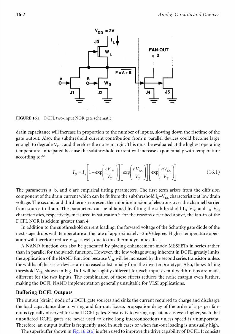
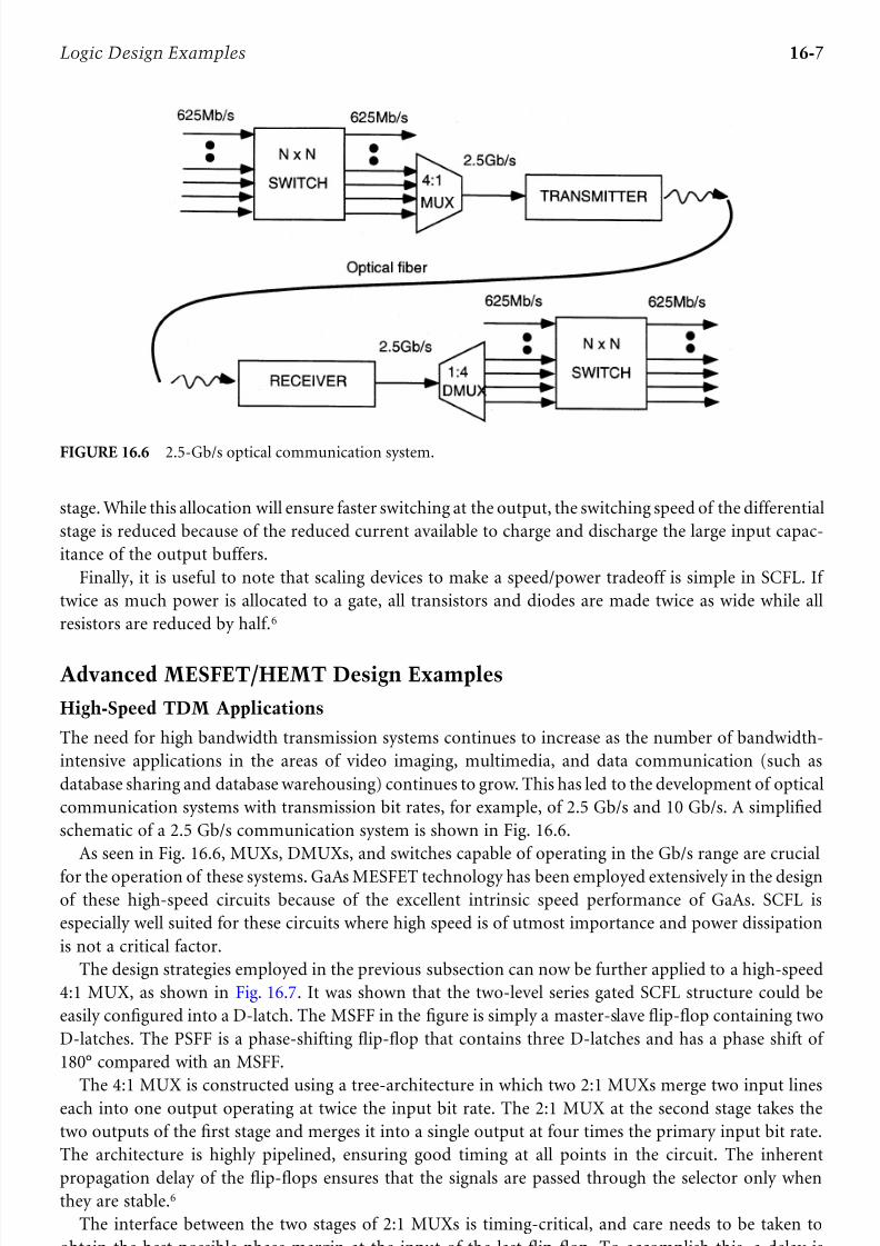
16 Logic Design Examples Design of MESFET and HEMT Logic Cir cuits ..............16-1 Direct-Coupled FET Logic (DCFL) • Source-Coupled FET Logic (SCFL) • Advanc ed MESFET/HEMT Design Examples 16.2 HBT L ogic Desi gn Exampl es.......................................... 16-10 III-V HBT for Circuit Designers • Current-Mode Logic • Emitter-C oupled Logic • ECL/CML Logic Examples • Advanc ed ECL/CML Logic Examples • HBT Circuit Design Examples 16.1 Desig n of MESFE T and HEMT Logic Circuits The basis of dc design, definition of logic levels, noise margin, and transfer characteristics were discussed in Chapter 16 using a DCFL and SCFL inverter as examples. In addition, methods for analysis of high- of GaAs MESFET, HEMT, or P-HEMT logic circuits with depletion-mode, enhancement-mode, or mixed E/D FETs. Several circuit topologies have been used for GaAs MESFETs, like direct-coupled FET logic (DCFL), source-coupled FET logic (SCFL), as well as dynamic logic families, 1 and have been extended for use with heterostructure FETs. Depending on the design requirements, whether it be high speed or low power , the designer can adjust the power -delay product by choosing the appropriate device technol- ogy and circuit topology, and making the correct design tradeoffs. Direct-Coupled FET Logic (DCFL) Among the numerous GaAs logic families, DCFL has emerged as the most popular log ic family for high - complexity, low-power LSI/VLSI circuit applications. DCFL is a simple enhancement/depletion-mode static ratioed GaAs logic family capable of VLSI densities due to its compactness and low power dissi- pation. An example demonstrating DCFL’s density is Vitesse Semiconductor’s 350K sea-of-gates array. The array uses a two-input DCFL NOR as the basic logic structure. The number of usable gates in the array is 175,000. A typical gate delay is specified at 95 ps with a power dissipation of 0.59 mW for a buffered two-input NOR gate with a fan-out of three, driving a wire load of 0.51 mm. 2 However, a drawback of DCFL is its low noise margin, the logic swing being approximately 600 mV. This makes the logic sensitive to changes in threshold voltage and ground bus voltage shifts. DCFL NOR and NAND Gate The DCFL inverter can easily be modified to perform the NOR function by placing additional enhance- If any input rises to V OH , the output will drop to V OL . If n inputs are high simultaneously, then V OL will be decreased because the width ratio W 1 /W L in Fig. 16.2 has effectively increased by a factor of n. There is a limit to the number of devices that can be placed in parallel to form very wide NOR functions. The Charles E. Chang Conexant Systems, Inc. Meera Venkataraman Troika Networks, Inc. Stephen I. Long University of California at Santa Barbara GaAs logic family, and the circuit diagram of a DCFL inverter was shown in Fig. 16.2. DCFL is the only ment-mode MESFETs in parallel as switch devices. A DCFL two-input NOR gate is shown in Fig. 16.1. speed performance of logic circuits were presented. These techniques can be further applied to th e design 16.1
Transcript of Analog Circuits and Devices

8/8/2019 Analog Circuits and Devices
http://slidepdf.com/reader/full/analog-circuits-and-devices 1/26
8/8/2019 Analog Circuits and Devices
http://slidepdf.com/reader/full/analog-circuits-and-devices 2/26

8/8/2019 Analog Circuits and Devices
http://slidepdf.com/reader/full/analog-circuits-and-devices 3/26

8/8/2019 Analog Circuits and Devices
http://slidepdf.com/reader/full/analog-circuits-and-devices 4/26

8/8/2019 Analog Circuits and Devices
http://slidepdf.com/reader/full/analog-circuits-and-devices 5/26

8/8/2019 Analog Circuits and Devices
http://slidepdf.com/reader/full/analog-circuits-and-devices 6/26
8/8/2019 Analog Circuits and Devices
http://slidepdf.com/reader/full/analog-circuits-and-devices 7/26

8/8/2019 Analog Circuits and Devices
http://slidepdf.com/reader/full/analog-circuits-and-devices 8/26

8/8/2019 Analog Circuits and Devices
http://slidepdf.com/reader/full/analog-circuits-and-devices 9/26

8/8/2019 Analog Circuits and Devices
http://slidepdf.com/reader/full/analog-circuits-and-devices 10/26

8/8/2019 Analog Circuits and Devices
http://slidepdf.com/reader/full/analog-circuits-and-devices 11/26

8/8/2019 Analog Circuits and Devices
http://slidepdf.com/reader/full/analog-circuits-and-devices 12/26

8/8/2019 Analog Circuits and Devices
http://slidepdf.com/reader/full/analog-circuits-and-devices 13/26

8/8/2019 Analog Circuits and Devices
http://slidepdf.com/reader/full/analog-circuits-and-devices 14/26

8/8/2019 Analog Circuits and Devices
http://slidepdf.com/reader/full/analog-circuits-and-devices 15/26

8/8/2019 Analog Circuits and Devices
http://slidepdf.com/reader/full/analog-circuits-and-devices 16/26

8/8/2019 Analog Circuits and Devices
http://slidepdf.com/reader/full/analog-circuits-and-devices 17/26

8/8/2019 Analog Circuits and Devices
http://slidepdf.com/reader/full/analog-circuits-and-devices 18/26

8/8/2019 Analog Circuits and Devices
http://slidepdf.com/reader/full/analog-circuits-and-devices 19/26

8/8/2019 Analog Circuits and Devices
http://slidepdf.com/reader/full/analog-circuits-and-devices 20/26

8/8/2019 Analog Circuits and Devices
http://slidepdf.com/reader/full/analog-circuits-and-devices 21/26

8/8/2019 Analog Circuits and Devices
http://slidepdf.com/reader/full/analog-circuits-and-devices 22/26

8/8/2019 Analog Circuits and Devices
http://slidepdf.com/reader/full/analog-circuits-and-devices 23/26

8/8/2019 Analog Circuits and Devices
http://slidepdf.com/reader/full/analog-circuits-and-devices 24/26

8/8/2019 Analog Circuits and Devices
http://slidepdf.com/reader/full/analog-circuits-and-devices 25/26
8/8/2019 Analog Circuits and Devices
http://slidepdf.com/reader/full/analog-circuits-and-devices 26/26