AN4768 Application note - STMicroelectronics · AN4768 Application note ... NTC thermistor and...
78
Introduction The SLLIMM™ (small low-loss intelligent molded module) 2 nd series is ST’s new family of compact, high efficiency, dual-in-line intelligent power modules, with optional extra features. This family is designed with a new internal configuration with only two drivers: one high-side driver and one low-side driver. This new approach allows a more compact package and, thanks to the new features provided by low-side driver, advanced protection functions. In addition, this new product offers the best compromise between conduction and switching energy with outstanding robustness and EMI behavior, rendering it ideal for improving efficiency for compressors, pumps, fans and low power motors working up to 20 kHz in hard-switching circuitries. Two IPM package versions are available: the full molded and the DBC (Direct Bonded Copper); both compatible with each other. This new series both complements and surpasses the original SLLIMM series in terms of features, package types and flexibility. The SLLIMM™ 2 nd series features: • two different package technologies: DBC for improved thermal behavior, and fully molded for a cost effective solution (both compatible with each other) • improved thermal performance (up to 20% thermal resistance reduction for DBC version) • trench field stop (TFS) IGBT technology for efficiency improvement • higher max. junction temperature of power chips (175 °C) • newly developed high-side and low-side driver pin-out arrangement for easier PCB routing • expanded line-up to 35 A • two different temperature monitoring options: NTC thermistor and thermal sensor • two fault events with signal output: overcurrent and undervoltage lockout The SLLIMM 2 nd series product family combines optimized silicon chips, integrated into three main inverter blocks: • power stage – six short-circuit rugged IGBTs in TFS technology and six freewheeling diodes • driving network – two differents low and high voltage gate drivers – three bootstrap diodes • protection and optional features – comparators for fault protection against overcurrent and short-circuit – two temperature monitoring options: output thermal sensor (TSO) embedded on the low-side gate driver and NTC thermistor (optional) – two fault event types with fault signal output: overcurrent and undervoltage – smart shutdown function and undervoltage lockout on V CC and V boot voltages The aim of this application note is to provide a detailed description of the new products family, providing the guidelines to the motor drive designers for an efficient, reliable, and fast design when using the 2 nd series of ST SLLIMM family. SLLIMM™ 2 nd series small low-loss intelligent molded module AN4768 Application note AN4768 - Rev 4 - May 2018 For further information contact your local STMicroelectronics sales office. www.st.com
Transcript of AN4768 Application note - STMicroelectronics · AN4768 Application note ... NTC thermistor and...

IntroductionThe SLLIMM™ (small low-loss intelligent molded module) 2nd series is ST’s new family of compact, high efficiency, dual-in-lineintelligent power modules, with optional extra features. This family is designed with a new internal configuration with only twodrivers: one high-side driver and one low-side driver.
This new approach allows a more compact package and, thanks to the new features provided by low-side driver, advancedprotection functions. In addition, this new product offers the best compromise between conduction and switching energy withoutstanding robustness and EMI behavior, rendering it ideal for improving efficiency for compressors, pumps, fans and lowpower motors working up to 20 kHz in hard-switching circuitries.
Two IPM package versions are available: the full molded and the DBC (Direct Bonded Copper); both compatible with eachother.
This new series both complements and surpasses the original SLLIMM series in terms of features, package types and flexibility.
The SLLIMM™ 2nd series features:• two different package technologies: DBC for improved thermal behavior, and fully molded for a cost effective solution (both
compatible with each other)• improved thermal performance (up to 20% thermal resistance reduction for DBC version)• trench field stop (TFS) IGBT technology for efficiency improvement• higher max. junction temperature of power chips (175 °C)• newly developed high-side and low-side driver pin-out arrangement for easier PCB routing• expanded line-up to 35 A• two different temperature monitoring options: NTC thermistor and thermal sensor• two fault events with signal output: overcurrent and undervoltage lockout
The SLLIMM 2nd series product family combines optimized silicon chips, integrated into three main inverter blocks:• power stage
– six short-circuit rugged IGBTs in TFS technology and six freewheeling diodes• driving network
– two differents low and high voltage gate drivers– three bootstrap diodes
• protection and optional features– comparators for fault protection against overcurrent and short-circuit– two temperature monitoring options: output thermal sensor (TSO) embedded on the low-side gate driver and NTC
thermistor (optional)– two fault event types with fault signal output: overcurrent and undervoltage– smart shutdown function and undervoltage lockout on VCC and Vboot voltages
The aim of this application note is to provide a detailed description of the new products family, providing the guidelines to themotor drive designers for an efficient, reliable, and fast design when using the 2nd series of ST SLLIMM family.
SLLIMM™ 2nd series small low-loss intelligent molded module
AN4768
Application note
AN4768 - Rev 4 - May 2018For further information contact your local STMicroelectronics sales office.
www.st.com

1 Comparison of SLLIMM 1st and 2nd series
The principal differences between the SLLIMM 2nd series and the previous generation (SLLIMM 1st and 1.i series)are listed below.
Table 1. SLLIMM 1st and 2nd series differences
FeatureSLLIMM 1st series:
STGIPSxxK60yySTGIPLxxK60yy
SLLIMM 1.i series:
STGIPSxxC60yySTGIPLxxC60yy
SLLIMM 2nd series:
STGIFxxCH60yy
STGIBxxCH60yy
STGIBxxM60yy
IGBT technology Planar Trench field stop Trench field stop
Current capability IC(@25°C) 10 to 20 A 10 to 30 A 8 to 35 A
Max Tj power chips 150°C 150°C 175°C
Package SDIP-25L (DBC)
SDIP-38L (DBC)
SDIP-25L (DBC)
SDIP-38L (DBC)
SDIP2F-26L (full molded)
SDIP2B-26L (DBC)
Number of leads 25/38 25/38 26
Control ICs 3 x half bridge IC 3 x half bridge IC1 x triple high-side IC
1 x triple low-side IC
Fault event monitoring Overcurrent Overcurrent
Overcurrent.
Undervoltage
(with differing fault signal output timing)
Temperaturemonitoring options NTC (several PNs) NTC (several PNs)
Temperature sensor integrated TSO (allPNs).
NTC (STGIxyyCH60Tz)
Interlocking function Yes Yes No
Lead options Short leads Short leadsShort leads and emitter forward.
Long leads
VISO 2500 Vrms 2500 Vrms 1500 Vrms
Please refer to the relevant datasheets for more detailed device specifications and recommended operationconditions.
1.1 Product synopsisThe SLLIMM 2nd series family has been designed to satisfy the requirements of a wide variety of final applicationsin the 300 W-3.0 kW range, including:• washing machines• dish washers• refrigerators• air conditioning compressor drives• sewing machines• pumps• tools
AN4768Comparison of SLLIMM 1st and 2nd series
AN4768 - Rev 4 page 2/78

• low power industrial applications
The main features and integrated functions can be summarized as follows:• 600 V, 8 - 35 A ratings• 3-phase IGBT inverter bridge including:
– six low-loss and short-circuit protected IGBTs– six low forward voltage drop and soft recovery freewheeling diodes
• two control ICs for gate driving and protection including:– three integrated bootstrap diodes– smart shutdown function– comparator for fault protection against overcurrent and short-circuit (on low-side gate driver IC)– undervoltage lockout on VCC (on high and low-side gate driver ICs) and Vboot (on high-side gate driver
ICs)– two fault signal outputs (on low-side gate driver IC): overcurrent protection and VCC undervoltage (on
low-side gate driver IC only)• output thermal sensor (TSO) embedded on the low-side gate driver IC• NTC thermistor for temperature monitor on the power stage (optional)• open emitter configuration for individual phase current sensing• DBC fully isolated package for enhanced thermal behavior and a cost-effective fully isolated full molded
package• isolation voltage rating of 1500 VRMS/min
The figure below shows the block diagram of an inverter solution including a SLLIMM.
AN4768Product synopsis
AN4768 - Rev 4 page 3/78
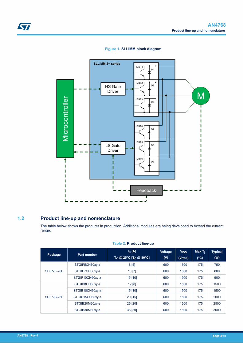
Figure 1. SLLIMM block diagram
HS GateDriver
SLLIMM 2nd series
LS GateDriver
IGBT4
IGBT5
IGBT6
D4
D5
D6
IGBT1
IGBT2
IGBT3
D1
D2
D3
Mic
roco
ntro
ller
Feedback
M
1.2 Product line-up and nomenclatureThe table below shows the products in production. Additional modules are being developed to extend the currentrange.
Table 2. Product line-up
Package Part numberIC (A)
TC @ 25°C [TC @ 80°C]
Voltage
(V)
VISO
(Vrms)
Max Tj
(°C)
Typical
(W)
SDIP2F-26L
STGIF5CH60xy-z 8 [5] 600 1500 175 750
STGIF7CH60xy-z 10 [7] 600 1500 175 800
STGIF10CH60xy-z 15 [10] 600 1500 175 900
SDIP2B-26L
STGIB8CH60xy-z 12 [8] 600 1500 175 1500
STGIB10CH60xy-z 15 [10] 600 1500 175 1500
STGIB15CH60xy-z 20 [15] 600 1500 175 2000
STGIB20M60xy-z 25 [20] 600 1500 175 2500
STGIB30M60xy-z 35 [30] 600 1500 175 3000
AN4768Product line-up and nomenclature
AN4768 - Rev 4 page 4/78

Table 3. Synoptic table for full molded package option
Feature STGIF5CH60xy-z STGIF7CH60xy-z STGIF10CH60xy-z
Voltage (V) 600 600 600
Continuous collector current each IGBT (A)
(TC = 25°C)8 10 15
Continuous collector current each IGBT (A)
(TC = 80°C)5 7 10
Rth(j-c) max single IGBT (°C/W) 5 4.8 4.6
Package type SDIP2F-26L SDIP2F-26L SDIP2F-26L
Number of pins26 (NTC on board) 26 (NTC on board) 26 (NTC on board)
25 25 25
Package size (mm) X, Y, Z 38.0x24.0x3.5 38.0x24.0x3.5 38.0x24.0x3.5
Integrated bootstrap diode Yes Yes Yes
SD function Yes Yes Yes
Comparator for fault protection Yes (1 pin) Yes (1 pin) Yes (1 pin)
Smart shutdown function Yes Yes Yes
Undervoltage lockout Yes Yes Yes
Open emitter configuration Yes (3 pins) Yes (3 pins) Yes (3 pins)
3.3/5 V input interface compatibility Yes Yes Yes
High and low-side IGBT input signal Active high Active high Active high
Table 4. Synoptic table for DBC package option
Feature STGIB8CH60xy-z STGIB10CH60xy-z STGIB15CH60xy-z STGIB20M60xy-z STGIB30M60xy-z
Voltage (V) 600 600 600 600 600
Continuous collectorcurrent each IGBT
(A)
(TC = 25°C)
12 15 20 25 35
Continuous collectorcurrent each IGBT
(A)
(TC = 80°C)
8 10 15 20 30
Rth(j-c) max singleIGBT (°C/W) 3 2.26 1.85 1.4 1.2
Package type SDIP2B-26L SDIP2B-26L SDIP2B-26L SDIP2B-26L SDIP2B-26L
Number of pins26 (NTC on board) 26 (NTC on board) 26 (NTC on board) 26 (NTC on board) 26 (NTC on board)
25 25 25 25 25
Package size (mm)X, Y, Z 38.0x24.0x3.5 38.0x24.0x3.5 38.0x24.0x3.5 38.0x24.0x3.5 38.0x24.0x3.5
Integrated bootstrapdiode Yes Yes Yes Yes yes
SD function Yes Yes Yes Yes yes
AN4768Product line-up and nomenclature
AN4768 - Rev 4 page 5/78
Feature STGIB8CH60xy-z STGIB10CH60xy-z STGIB15CH60xy-z STGIB20M60xy-z STGIB30M60xy-z
Comparator for faultprotection Yes (1 pin) Yes (1 pin) Yes (1 pin) Yes (1 pin) yes (1 pin)
Smart shutdownfunction Yes Yes Yes Yes yes
Undervoltage lockout yes yes yes yes yes
Open emitterconfiguration Yes (3 pins) Yes (3 pins) Yes (3 pins) Yes (3 pins) yes (3 pins)
3.3/5 V inputinterface compatibility Yes Yes Yes Yes yes
High and low-sideIGBT input signal active high active high active high active high active high
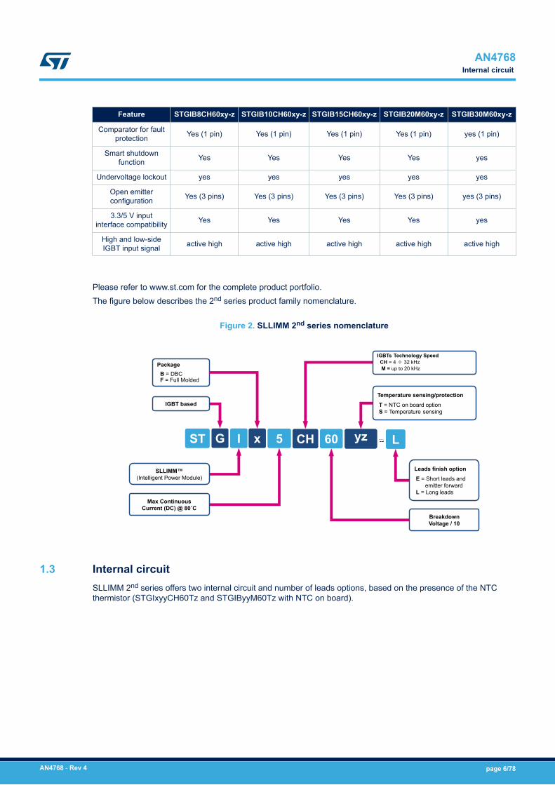
Please refer to www.st.com for the complete product portfolio.The figure below describes the 2nd series product family nomenclature.
Figure 2. SLLIMM 2nd series nomenclature
Temperature sensing/protectionT = NTC on board optionS = Temperature sensing
Leads finish optionE = Short leads and
emitter forwardL = Long leads
IGBTs Technology SpeedCH = 4 ÷ 32 kHzM = up to 20 kHz
PackageB = DBC F = Full Molded
5 CHyz
LI x
SLLIMM™(Intelligent Power Module)
Max ContinuousCurrent (DC) @ 80˚C
Breakdown Voltage / 10
ST 60G
IGBT based
yz
1.3 Internal circuitSLLIMM 2nd series offers two internal circuit and number of leads options, based on the presence of the NTCthermistor (STGIxyyCH60Tz and STGIByyM60Tz with NTC on board).
AN4768Internal circuit
AN4768 - Rev 4 page 6/78

Figure 3. Internal circuit for SDIP2F-26L and SDIP2B-26L (without NTC)
NC (1)
TSO (17)
CIN (15)
VCCL (13)
LINw (12)
LINv (11)LINu (10)
GND (16)
GND (9)
HINw (7)HINv (6)
HINu (5)
VBOOTw (4)
VBOOTv (3)
VBOOTu (2)
VCCH (8)
IGBT1
IGBT2
IGBT3
IGBT4
IGBT5
IGBT6
D1
D2
D3
D4
D5
D6
H-s
ide
L-si
de
SD /OD(14)
(26) NC (25) NC
(24) P
(23) U
(22) V
(21) W
(20) NU
(19) NV
(18) NW
AN4768Internal circuit
AN4768 - Rev 4 page 7/78

Figure 4. Internal circuit for SDIP2F-26L and SDIP2B-26L (with NTC)
NC (1)
TSO (17)
CIN (15)
VCCL (13)
LINw (12)
LINv (11)LINu (10)
GND (16)
GND (9)
HINw (7)HINv (6)
HINu (5)
VBOOTw (4)
VBOOTv (3)
VBOOTu (2)
VCCH (8)
IGBT1
IGBT2
IGBT3
IGBT4
IGBT5
IGBT6
D1
D2
D3
D4
D5
D6
H-s
ide
L-si
de
SD /OD(14)
(26) T1 (25) T2
(24) P
(23) U
(22) V
(21) W
(20) NU
(19) NV
(18) NW
1.4 Absolute maximum ratingsThe absolute maximum ratings represent the extreme capabilities of the device and can be normally used to setthe worst case design limit conditions.Absolute maximum values are based on specific test parameters such as temperature, frequency and voltage.Device performance can change according to the applied condition.The SLLIMM specifications are described below with the STGIF5CH60xy-z datasheet example. Please refer tothe relevant product datasheets for detailed information regarding the other device types.
Table 5. Inverter part of STGIF5CH60xy-z
Symbol Parameter Value Unit
VPN supply voltage applied between P - NU, NV, NW 450 V
VPN(surge) supply voltage surge between P - NU, NV, NW 500 V
VCES collector-emitter voltage each IGBT 600 V
AN4768Absolute maximum ratings
AN4768 - Rev 4 page 8/78

Symbol Parameter Value Unit
±ICeach IGBT continuous collector current at Tj = 25 °C 8 A
each IGBT continuous collector current at Tj = 80 °C 5 A
±ICP peak collector current each IGBT (less than 1ms) 16 A
PTOT each IGBT total dissipation at TC = 25 °C 30 W
tSCW short circuit withstand time, VCE= 300 V, TJ= 125 °C, VCC= Vboot = 15 V, VIN= 0 to 5 V 5 µs
The power stage of SLLIMM is based on IGBTs (and freewheeling diodes) with a 600 V VCES rating. Consideringthe SLLIMM internal stray inductance during the commutations, which can generate up to 100 V of surge voltage,the maximum surge voltage between P-N (VPN(surge)) allowed is 500 V. At the same time, the maximum supplyvoltage (in steady-state) applied between P-N (VPN) is limited to 450 V because of an additional 50 V surgevoltage generated by the stray inductance between the SLLIMM and the DC-link capacitor.±Ic is the allowable DC current continuously flowing at the collector electrode of each IGBT (Tj = 25 °C andTj = 80 °C).tSCW is the short-circuit, non repetitive withstand time.The internal SLLIMM layout and board layout shown below are the two major components of parasitic inductance.
AN4768Absolute maximum ratings
AN4768 - Rev 4 page 9/78

Figure 5. Stray inductance components of output stage
Parasitic inductancedue to PCB layout
P
N
U, V, W
HVIC
SLLIMM
to motor Vbus+
Parasitic inductancedue to the SLLIMM internal layout
The real voltage over the IGBT can exceed the rating voltage
Due to di/dt value and parasitic inductance the over-voltage spike can appear on the SLLIMM pins
VPN(surge)
Highdi/dtvalue
Flat VPNvalue
VPN
C
LVIC
The IGBTs incorporated in the SLLIMM are tailored for motor control applications where short-circuit self-protection is one of the main module features. If the short-circuit conditions exceed the above specifications, thelifetime of the device is drastically shortened. We therefore strongly recommended not operating the SLLIMMunder these conditions.
Table 6. Control part of STGIF5CH60xy-z
Symbol Parameter Min Max Unit
VCC supply voltage between VCCH-GND, VCCL-GND -0.3 20 V
VBOOT bootstrap voltage -0.3 619 V
VOUT output voltage between U, V, W and GND VBOOT- 21 VBOOT+ 0.3 V
VCIN comparator input voltage -0.3 20 V
VIN logic input voltage applied between HINx, LINx and GND -0.3 15 V
VSD/OD open-drain voltage -0.3 7 V
ISD/OD open-drain sink current - 10 mA
AN4768Absolute maximum ratings
AN4768 - Rev 4 page 10/78

Symbol Parameter Min Max Unit
VTSO temperature sensor output voltage -0.3 5.5 V
ITSO temperature sensor output current - 7 mA
VCC represents the supply voltage of the control part for both high-side and low-side gate drivers. Local filtering isrecommended to enhance the SLLIMM noise immunity. Generally, we suggest using one electrolytic capacitor(with a higher value and not negligible ESR) and a faster and smaller ceramic capacitor (in the order of hundredsof nF) to provide current.Refer to the details in the table below to drive the SLLIMM properly.
Table 7. Supply voltage and operation behavior
VCC voltage (typ. value) Operating behavior
< 12 V As the voltage is lower than the UVLO threshold, the control circuit is not fully turned on. Perfectfunctionality cannot be guaranteed.
12 V – 13.5 V IGBTs can function, however conduction and switching losses increase due to low voltage gatesignal.
13.5 V – 18 V Recommended value (see relevant datasheets).
18 V – 20 V IGBTs can function. Switching speed is faster and saturation current higher, increasing short-circuitbroken risk and EMI issues.
> 20 V Control circuit is destroyed. Absolute max. rating is 20V.
For further information, please refer to the relevant datasheet.
Table 8. Total STGIF5CH60xy-z system
Symbol Parameter Value Unit
VISO isolation withstand voltage applied between each pin and heatsink plate (AC voltage, t = 60 s) 1500 Vrms
Tj power chip operating junction temperature -40 to 175 °C
TC module case operation temperature -40 to 125 °C
The figure below shows the case temperature measurement point for all package options, right above the powerchip. To obtain accurate temperature information, mount a thermocouple on the heat sink surface at this specificlocation. For non-complementary switching schemes, the highest TC point occur in a different position. In thiscase, the measurement location is over the point where the highest power chip temperature is generated.
AN4768Absolute maximum ratings
AN4768 - Rev 4 page 11/78

Figure 6. TC measurement point
1.5 SCSOAFigure 7. SCSOA test circuit and Figure 8. SCSOA main data show the circuits for obtaining the SCSOA ofSLLIMM 2nd series devices and the SCSOA main data, respectively.
AN4768SCSOA
AN4768 - Rev 4 page 12/78
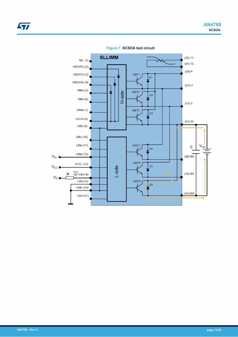
Figure 7. SCSOA test circuit
AN4768SCSOA
AN4768 - Rev 4 page 13/78

Figure 8. SCSOA main data
VPN is the surge voltage generated at the end of the switching by the inductor wiring between the IPM and DC-Link capacitor.Esc is the total energy during the switch.tsc is the impulse width.The following figures show the typical SCSOA performance curves of STGIF5CH60xy-z, STGIF7CH60xy-z,STGIFx10CH60xy-z, STGIB8CH60xy-z , STGIB15CH60xy-z, STGIB20M60xy-z and STGIB30M60xy-z devices.The testing conditions for all the devices are: Vbus = 300 V, Tcase = 125 °C, VIN = 5 V, non-repetitive.
Figure 9. Typical STGIF5CH60yy SCSOA curve
0
50
100
150
0 2 4 6 8 10
Isc[A]
tsc[µs]
Limited by maximum saturation current
Isat=72A @15V
Vcc=18V
Vcc=15V
Vcc=13V
AN4768SCSOA
AN4768 - Rev 4 page 14/78

Figure 10. Typical STGIF7CH60yy SCSOA curve
0
50
100
150
200
0 2 4 6 8 10
Isc[A]
tsc[µs]
Vcc=18V
Vcc=15V
Vcc=13VLimited by maximum saturation current
Isat=114A @15V
Figure 11. Typical STGIx10CH60yy SCSOA curve
0
50
100
150
200
250
0 2 4 6 8 10
Isc[A]
tsc[µs]
Limited by maximum saturation current
Isat=145A @15V
Vcc=18V
Vcc=15V
Vcc=13V
Figure 12. Typical STGIB8CH60yy SCSOA curve
0
50
100
150
0 2 4 6 8 10
Isc[A]
tsc[µs]
Vcc=18V
Vcc=15V
Vcc=13VLimited by maximum saturation current
Isat=90A @15V
AN4768SCSOA
AN4768 - Rev 4 page 15/78

Figure 13. Typical STGIB15CH60yy SCSOA curve
0
50
100
150
200
250
300
350
0 2 4 6 8 10
Isc[A]
tsc[µs]
Limited by maximum saturation current
Isat=210A @15V
Vcc=18V
Vcc=15V
Vcc=12.4V
Figure 14. Typical STGIB20M60yy SCSOA curve
0
50
100
150
200
0 2 4 6 8 10 12 14
Isc[A]
tsc[µs]
Limited by maximum saturation current
Isat=105A @15V
Vcc=18V
Vcc=15V
Vcc=12.4V
Figure 15. Typical STGIB30M60yy SCSOA curve
0
50
100
150
200
250
0 2 4 6 8 10 12 14 16
Isc[A]
tsc[µs]
Limited by maximum saturation current
Isat=147A @15V
Vcc=18V
Vcc=15V
Vcc=12.4V
AN4768SCSOA
AN4768 - Rev 4 page 16/78

2 Electrical characteristics and functions
In this section, the main electrical characteristics of the power stage are discussed, together with a detaileddescription of the SLLIMM functions.
2.1 IGBTsThe 2nd version of the SLLIMM range combines the IGBTs with trench field stop (TFS) technology (in both H andM series), along with a new gate driver design to improve the system efficiency and allow new features.These power devices, optimized for typical motor control switching frequencies, offer an excellent tradeoffbetween voltage drop (VCE(sat)) and switching speed (tfall) to therefore minimize the two major sources of energyloss, conduction and switching, thus reducing the environmental impact of daily-use equipment. Furthermore, theTFS technology offers significant improvement in terms of loss reduction over the previous generation based onplanar technology. The figure below shows a comparison of VCE(sat) vs. EOFF for both TFS and planar IGBTtechnologies with the same chip size.
Figure 16. TFS and Planar IGBT technology comparison
SLLIMM 2nd series devices are also capable of surviving short-circuits lasting up to 5 microseconds, as requiredby targeted applications. Furthermore M series devices (STGIB20M60xy-z and STGIB30M60xy-z) have a shortcircuit current withstand time of 8 microseconds.
2.2 Freewheeling diodesThe Turbo 2 ultrafast high voltage diodes have been appropriately selected for the SLLIMM family and carefullytuned to achieve the best trr/VF tradeoff and softness as freewheeling diodes in order to further improve the totalperformance of the inverter and significantly reduce electromagnetic interference (EMI) in motor controlapplications, which are quite sensitive to this phenomena.
AN4768Electrical characteristics and functions
AN4768 - Rev 4 page 17/78
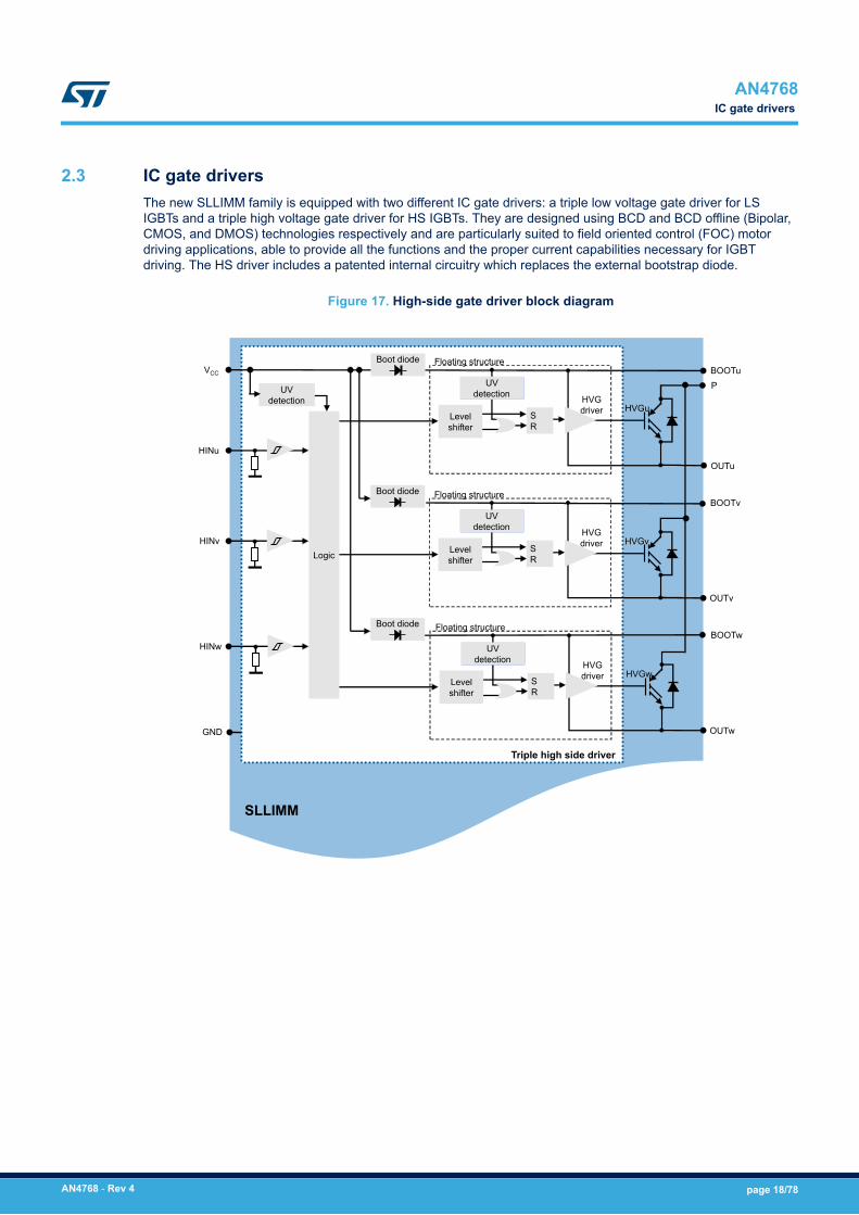
2.3 IC gate driversThe new SLLIMM family is equipped with two different IC gate drivers: a triple low voltage gate driver for LSIGBTs and a triple high voltage gate driver for HS IGBTs. They are designed using BCD and BCD offline (Bipolar,CMOS, and DMOS) technologies respectively and are particularly suited to field oriented control (FOC) motordriving applications, able to provide all the functions and the proper current capabilities necessary for IGBTdriving. The HS driver includes a patented internal circuitry which replaces the external bootstrap diode.
Figure 17. High-side gate driver block diagram
UVDETECTION
PBOOTu
HINu
VCC
Level shifter
UVdetection
SR
Floating structure
HVGdriver
Boot diode
HVGu
OUTu
UVDETECTION
BOOTv
Level shifter
UVdetection
SR
Floating structure
HVGdriver HVGv
OUTv
HINv
UVDETECTION
BOOTw
Logic
Level shifter
UVdetection
SR
Floating structure
HVGdriver HVGw
OUTw
HINw
Triple high side driver
SLLIMM
GND
Boot diode
Boot diode
UVdetection
AN4768IC gate drivers
AN4768 - Rev 4 page 18/78

Figure 18. Low-side gate driver block diagram
LINu
VCC
Logic
LVGdriver LVGu
Triple low side driver
SLLIMM
UVdetection
LINv
LINw
SMARTSD
+5V
OUTu
Nu
LVGdriver LVGv
OUTv
Nv
LVGdriver LVGw
OUTw
Nw
SD/OD
UVLO
TEMPSENSORTSO
GND VREF
+
-
CIN
+
VCC
VCC
VCC
For pin descriptions, refer to Section 3.4 Input and output pin descriptions.
2.3.1 Logic inputsAll the logic inputs include hysteresis (~1V) for low noise sensitivity and are TTL/CMOS-3.3-V compatible. Thanksto this low voltage interface logic compatibility, the SLLIMM can be used with any kind of high performancecontroller like microcontrollers, DSPs or FPGAs.As shown in Figure 17. High-side gate driver block diagram and Figure 18. Low-side gate driver block diagram,the logic inputs have internal pull-down resistors in order to set the proper logic level in case of interruption in thelogic lines. If logic inputs are left floating, the gate driver outputs LVG and HVG are set to low level. This simplifiesthe interface circuit by eliminating the six external resistors, therefore saving on cost, board space and number ofcomponents.
AN4768IC gate drivers
AN4768 - Rev 4 page 19/78
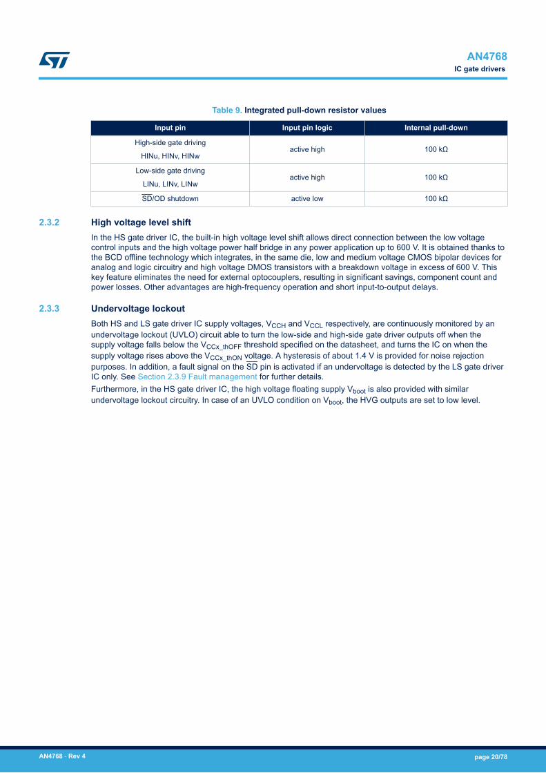
Table 9. Integrated pull-down resistor values
Input pin Input pin logic Internal pull-down
High-side gate driving
HINu, HINv, HINwactive high 100 kΩ
Low-side gate driving
LINu, LINv, LINwactive high 100 kΩ
SD/OD shutdown active low 100 kΩ
2.3.2 High voltage level shiftIn the HS gate driver IC, the built-in high voltage level shift allows direct connection between the low voltagecontrol inputs and the high voltage power half bridge in any power application up to 600 V. It is obtained thanks tothe BCD offline technology which integrates, in the same die, low and medium voltage CMOS bipolar devices foranalog and logic circuitry and high voltage DMOS transistors with a breakdown voltage in excess of 600 V. Thiskey feature eliminates the need for external optocouplers, resulting in significant savings, component count andpower losses. Other advantages are high-frequency operation and short input-to-output delays.
2.3.3 Undervoltage lockoutBoth HS and LS gate driver IC supply voltages, VCCH and VCCL respectively, are continuously monitored by anundervoltage lockout (UVLO) circuit able to turn the low-side and high-side gate driver outputs off when thesupply voltage falls below the VCCx_thOFF threshold specified on the datasheet, and turns the IC on when thesupply voltage rises above the VCCx_thON voltage. A hysteresis of about 1.4 V is provided for noise rejectionpurposes. In addition, a fault signal on the SD pin is activated if an undervoltage is detected by the LS gate driverIC only. See Section 2.3.9 Fault management for further details.Furthermore, in the HS gate driver IC, the high voltage floating supply Vboot is also provided with similarundervoltage lockout circuitry. In case of an UVLO condition on Vboot, the HVG outputs are set to low level.
AN4768IC gate drivers
AN4768 - Rev 4 page 20/78

Figure 19. Timing chart of undervoltage lockout function on low-side section
Time t2 t3 t4
RESETCircuit state
t1
SETRESET
≈≈
≈≈
VCCL_thON
VCCL_thOFF
IC
VCC
LIN
RESETSDSET
RESET
≈
t5 t6
VCCL_thON
The timing chart is based on the following steps:• t1: when the VCC supply voltage rises above the VCCL_thON threshold, the low-side gate driver starts
operating after the next input signal LIN is on. The SD signal is in the pull up condition (RESET) from theexternal network and the circuit state is RESET.
• t2: input signal LIN is on and the related IGBT is turned on.• t3: when the VCC supply voltage falls below the VCCL_thOFF threshold, an UVLO event is detected. The LS
IGBTs are turned off even if the input signals LIN from the MCU are switching. The SD signal jumps to theSET condition and circuit is now in the SET state.
• t4: at this time, the VCC supply voltage rises above the VCCL_thON threshold again, but the driver is waitingfor the SD reset. During this time, despite the VCC having the right voltage, the LIN signals coming from theMCU are filtered. The SD is in the SET condition and fault information is sent to the MCU. The circuit statechanges to RESET.
• t5: the LS gate driver re-starts when the SD jumps to the RESET condition.• t6: the first useful input signal LIN now is able to turn on the LS IGBTs.
The undervoltage event on the LS gate driver enables a fault signal on the SD pin with a specific interval (t4 - t3):• SD is SET for tUVLO (70 μs) in case of short UVLO event (≤ 70 μs)• SD is SET for tUVLO (> 70 μs) in case of long UVLO event (> 70 μs)
Further details regarding SD timing can be found in Section 2.3.9 Fault management.
AN4768IC gate drivers
AN4768 - Rev 4 page 21/78

Figure 20. Timing chart of undervoltage lockout function on high-side section
Time t2 t3 t4
RESETCircuit state
t1
SETRESET
≈≈
≈≈
VCCH/BS_thON
VCCH/BS_thOFF
IC
VCC/VBS
HIN
RESETSD
≈t5
VCCH/BS_thON
The timing chart applies to the high-side gate driver for an undervoltage on VCC or Vboot. It is based on thefollowing steps:• t1: when the VCC (or Vboot) supply voltage rises above the VCCH_thON (or VBS_thON) threshold(s), the HS
gate driver starts operating after the next input signal HIN is on. The SD signal is in the pull up condition(RESET) from the external network and the circuit state changes to RESET.
• t2: input signal HIN is on and the IGBTs are turned on.• t3: when the VCC (or Vboot) supply voltage falls below the VCCH_thOFF (or VBS_thOFF) threshold(s), an UVLO
event is detected. The HS IGBTs are turned off even if the HIN input signals from the MCU are switching.The circuit changes to the SET state. During UVLO on the HS section, there is no fault signal so the SDremains in the RESET condition.
• t4: at this time, the VCC (or Vboot) supply voltage again rises above the VCCH_thON (or VBS_thON) thresholdand the gate driver restarts.
• t5: the first useful input signal HIN now is able to turn on the IGBT.
Table 10. SD duration time per event summarizes the possible UVLO events and their effect on the IGBTs and theSD pin.
2.3.4 Comparators for fault sensingThe SLLIMM family integrates one comparator intended for advanced fault protection such as overcurrent, overtemperature or any other type of fault measurable via a voltage signal. The comparator has an internal referencevoltage VREF, specified in the datasheet, on its inverting input (see Low-side gate driver block diagram), while thenon-inverting input is available on the CIN pin. The comparator input can be connected to an external shuntresistor to implement a simple overcurrent or short-circuit detection function, as discussed in the following section.
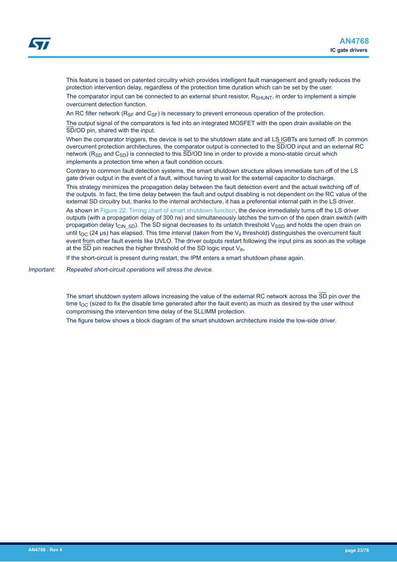
2.3.5 Short-circuit protection and smart shutdown functionThe SLLIMM is able to monitor the output current and provide protection against overcurrent and short-circuitconditions in a very short time (comparator triggering to high/low-side driver turn-off propagation delaytisd = 300 ns), thanks to the smart shutdown function.
AN4768IC gate drivers
AN4768 - Rev 4 page 22/78
This feature is based on patented circuitry which provides intelligent fault management and greatly reduces theprotection intervention delay, regardless of the protection time duration which can be set by the user.The comparator input can be connected to an external shunt resistor, RSHUNT, in order to implement a simpleovercurrent detection function.An RC filter network (RSF and CSF) is necessary to prevent erroneous operation of the protection.The output signal of the comparators is fed into an integrated MOSFET with the open drain available on theSD/OD pin, shared with the input.When the comparator triggers, the device is set to the shutdown state and all LS IGBTs are turned off. In commonovercurrent protection architectures, the comparator output is connected to the SD/OD input and an external RCnetwork (RSD and CSD) is connected to this SD/OD line in order to provide a mono-stable circuit whichimplements a protection time when a fault condition occurs.Contrary to common fault detection systems, the smart shutdown structure allows immediate turn off of the LSgate driver output in the event of a fault, without having to wait for the external capacitor to discharge.This strategy minimizes the propagation delay between the fault detection event and the actual switching off ofthe outputs. In fact, the time delay between the fault and output disabling is not dependent on the RC value of theexternal SD circuitry but, thanks to the internal architecture, it has a preferential internal path in the LS driver.As shown in Figure 22. Timing chart of smart shutdown function, the device immediately turns off the LS driveroutputs (with a propagation delay of 300 ns) and simultaneously latches the turn-on of the open drain switch (withpropagation delay tCIN_SD). The SD signal decreases to its unlatch threshold VSSD and holds the open drain onuntil tOC (24 μs) has elapsed. This time interval (taken from the Vil threshold) distinguishes the overcurrent faultevent from other fault events like UVLO. The driver outputs restart following the input pins as soon as the voltageat the SD pin reaches the higher threshold of the SD logic input Vih.If the short-circuit is present during restart, the IPM enters a smart shutdown phase again.
Important: Repeated short-circuit operations will stress the device.
The smart shutdown system allows increasing the value of the external RC network across the SD pin over thetime tOC (sized to fix the disable time generated after the fault event) as much as desired by the user withoutcompromising the intervention time delay of the SLLIMM protection.The figure below shows a block diagram of the smart shutdown architecture inside the low-side driver.
AN4768IC gate drivers
AN4768 - Rev 4 page 23/78
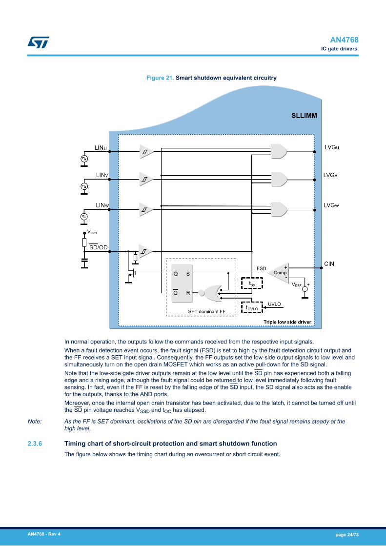
Figure 21. Smart shutdown equivalent circuitry
In normal operation, the outputs follow the commands received from the respective input signals.When a fault detection event occurs, the fault signal (FSD) is set to high by the fault detection circuit output andthe FF receives a SET input signal. Consequently, the FF outputs set the low-side output signals to low level andsimultaneously turn on the open drain MOSFET which works as an active pull-down for the SD signal.Note that the low-side gate driver outputs remain at the low level until the SD pin has experienced both a fallingedge and a rising edge, although the fault signal could be returned to low level immediately following faultsensing. In fact, even if the FF is reset by the falling edge of the SD input, the SD signal also acts as the enablefor the outputs, thanks to the AND ports.Moreover, once the internal open drain transistor has been activated, due to the latch, it cannot be turned off untilthe SD pin voltage reaches VSSD and tOC has elapsed.
Note: As the FF is SET dominant, oscillations of the SD pin are disregarded if the fault signal remains steady at thehigh level.
2.3.6 Timing chart of short-circuit protection and smart shutdown functionThe figure below shows the timing chart during an overcurrent or short circuit event.
AN4768IC gate drivers
AN4768 - Rev 4 page 24/78

Figure 22. Timing chart of smart shutdown function
The timing chart is based on the following steps:• t1: when the output current is lower than the max. allowed level, the SLLIMM functions normally.• t2: when the output current reaches the max. allowed level (ISC), the overcurrent/short-circuit event is
detected and the protection is activated. The voltage across the shunt resistor, and then on the CIN pin(VCIN), reaches the VREF value; the comparator triggers and the shutdown phase begins.
• t3: after tcin_SD time, the M1 internal open-drain MOSFET is switched on, the SD starts the discharge phase(with a time constant according to Equation 1) and the smart shutdown switches off the low-side IGBTs gate(LVG) through a preferential path (400 ns as typical internal delay time).
Equation 1 τA ≅ RONOD//RSD ∙ CSD• t4: at this time, the SD signal reaches the low voltage logic level (Vil) and, starting from this point, an internal
timer fixes the tOC time (20 μs for an overcurrent or short-circuit event).• t5: the SD signal reaches the Smart SD unlatch threshold (VSSD). In the meantime, the MCU detects the
fault and it switches the input signals LIN and HIN off. The open drain MOSFET M1 remains on.• t6: when the tOC has elapsed, the SD can rise with a time constant given by following equation:
Equation 2 τB ≅ RPD_SD//RSD ∙ CSD• t7: the SD signal reaches the upper threshold Vih (in the worst case) and the system is ready to be re-
enabled.
The discharging time tA and the charging time tB are the time intervals between t5-t3 and t7-t6, respectively.
2.3.7 Current sensing shunt resistor selectionAs previously discussed, the shunt resistors RSHUNT externally connected between the N pins and ground areused in the overcurrent detection circuitry.
AN4768IC gate drivers
AN4768 - Rev 4 page 25/78

When the output current exceeds the short-circuit reference level (ISC), the CIN signal overtakes the VREF valueand the short-circuit protection is activated. For reliable and stable operation, the current sensing resistor shouldbe a high quality, low tolerance non-inductive type. In fact, stray inductance in the circuit due to the layout, the RCfilter, and even the shunt resistor, must be minimized in order to avoid undesired short-circuit detection.For these reasons, the shunt resistor and the filtering components must be placed as close as possible to theSLLIMM pins. Refer to layout suggestionsThe value of the current sense resistor can be calculated according to different guidelines, functions of the designspecifications, or requirements. A common criterion is presented here based on the following steps:• Define of the overcurrent threshold value (IOC_th). This value can, for example, be set by considering the
IGBT typical working current in the application and adding 20-30% as overcurrent.• Calculation of the shunt resistor value according to the conditioning network.• Selection of the closest shunt resistor commercial value.• Calculation of the power rating of the shunt resistor, taking into account that this parameter is strongly
temperature dependent. Therefore, the power derating ratio of the shunt resistor, ΔP(T)%, shown in themanufacturer’s datasheet, must be considered, as shown in the formula below:
Equation 3
PSHUNT T = RSHUNT ∙ IRMS2∆P T %Where IRMS is the IGBT RMS working current.For proper selection of the shunt resistor, a safety margin of at least 30% is recommended on the calculatedpower rating.Below is an example for STGIF5CH60xy-z IPM.The value of shunt resistor is calculated by the following equation:Equation 4 RSH = VrefIOCWhere Vref is the internal comparator (CIN) (0.51 V typ.) and IOC is the OC trigger level.The maximum OC protection level should be set less than the pulsed collector current in the datasheet. In thisdesign, the overcurrent threshold level is fixed at 30% more than the nominal current at 80 °C (5 A). Therefore theshunt resistor value is:Equation 5 RSH = VrefIOC = 0.511.3x5 = 0.078 ΩFor the power rating of the shunt resistor, these parameters must be considered:• maximum load current of inverter (85% of Inom (Arms)): Iload(max).• shunt resistor value at TC=25°C.• power derating ratio of shunt resistor at TSH = 100 °C• safety margin.
The power rating is calculated with following equation:Equation 6 PSH = 12 ∙ Iload max2 ∙ RSH ∙ marginDerating ratioFor STGIF5CH60xy-z and RSH= 0.08 Ω (commercial value):Equation 7 Inom = 5A @80°C Inom rms = Inom2 Iload max = 85% Inom rms = 3Arms• power derating ratio of shunt resistor at TSH =100 °C: 80% (from datasheet manufacturer)• safety margin: 30%
AN4768IC gate drivers
AN4768 - Rev 4 page 26/78

Equation 8 PSH = 12 ∙ 32 ∙ 0.08 ∙ 1.30.8 = 0.58W2.3.8 RC filter network selection
Two options of shunt (1- or 3-shunt) resistor circuits can be adopted for different control and short-circuitprotection techniques. For 3-shunt resistor configurations, the following figure shows two simple overcurrentprotection variants: type A, using an additional shunt resistor (RSHUNT) and type B, using a diode OR gate circuit.
Figure 23. Examples of SC protection circuits
SLLIMM
CSF
RSF
RSHUNT
CIN
NW
NU
NV
RSHUNT_U
RSHUNT_W
RSHUNT_V
3-shunt resistors circuit – type A
SLLIMM
CSF
RSF
RSHUNT
CIN
NW
NUNV
1-shunt resistor circuit
SLLIMM
CSF
RSF
CIN
NW
NU
NV
3-shunt resistors circuit – type B
D1
D2
D3
RSHUNT_U,V,W
An RC filter network is required to prevent undesired short-circuit operation due to noise on the shunt resistor.All the solutions allow detection of the total current in all the three phases of the inverter. The filter is based on theRSF and CSF network and its time constant is given by:Equation 9 tSF = RSF ∙ CSFIn addition to the RC time constant, the turn-off propagation delay of the gate driver, tCIN_LVG (specified in thedatasheet) and the IGBT turn-off time (in the order of tens of ns), must be considered in the total delay time(tTotal), which is the time necessary to completely switch the IGBT off once the short-circuit event is detected.Therefore, tTotal is calculated as follows:Equation 10 tTotal = tSF + tCIN_LVG + toffConsidering that the IGBT short-circuit withstand time (tSC) is 5 µs, tSF should be set to the 1-2 µs range.In a 3-shunt resistor circuit, a specific control technique can be implemented by using the three shunt resistors(RSHUNT_U, RSHUNT_V and RSHUNT_W) to monitor each phase current.An example short-circuit event during normal operation, between P and OUTx when LINx is high, is shown in thefigure below.
AN4768IC gate drivers
AN4768 - Rev 4 page 27/78

Figure 24. Example of a short-circuit event
Logic
Triple low side driver
SLLIMM
LINx
SMARTSD
+5V
LVGdriver LVGx
OUTx
Nx
SD/OD
UVLO
TEMPSENSOR
TSO
GNDVREF
+
-
CIN
VCC
UVDETECTION
P
BOOTx
HINx
VCC
Level shifter
UVdetection
SR
Floating structure
HVGdriver
Boot diode
HVGx
Logic
UVdetection
Triple high side driver
from mC
from mC
RSD
CSD
from mC
RSF
CSFVCIN
RSHUNT
SC event onhigh side
ISC
+
Smart shutdown operation clearly demonstrates the highly rapid protection offered by the smart shutdownfunction for an overcurrent fault event occurring on an HS IGBT.The main steps are, shown in the figure below, are:• t1: collector current IC starts to rise. An SC event is not detected yet due to the RC network on the CIN pin• t2: voltage on VCIN reaches VREF. An SC event is detected and the smart shutdown starts turning off the LS
IGBTs. The SD signal is enabled (for 24 μs) so the MCU can stop the PWM signals and as consequence ofthis, even the HS IGBTs are turned off.
• t3: the SLLIMM is definitively turned off in less than 400 ns (including the td(off) time of IGBT) from SCdetection.
In summary, the total disable time is t3-t2 and the total SC action time is t3-t1.
AN4768IC gate drivers
AN4768 - Rev 4 page 28/78
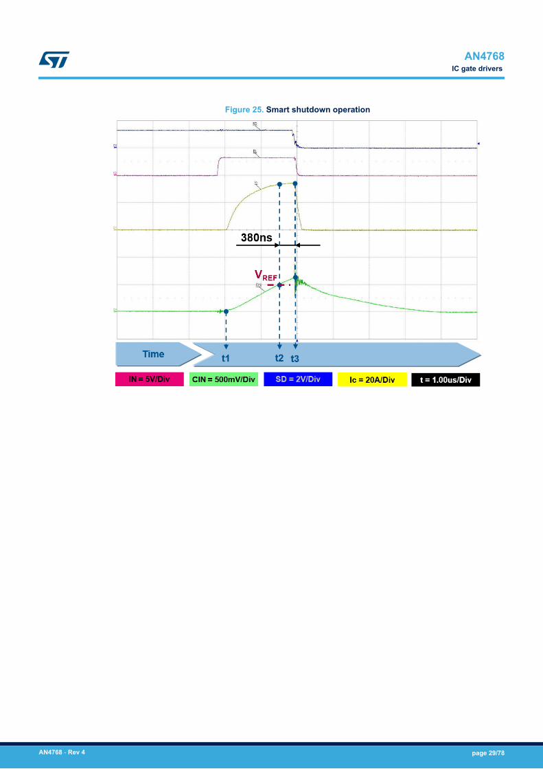
Figure 25. Smart shutdown operation
AN4768IC gate drivers
AN4768 - Rev 4 page 29/78

2.3.9 Fault managementThe SLLIMM 2nd series integrates a specific kind of fault management, useful when the SD pin acts as output andis able to identify the type of fault event.As previously described, as soon as a fault occurs, the open-drain (DMOS) is activated and LVG outputs areforced low and consequently the LS IGBTs.Two types of fault can be identified:• Overcurrent (OC) sensed by the internal comparator (CIN)• Undervoltage (UVLO) on LS gate driver supply voltage (VCCL)
During an UVLO event, the supply voltage must in any case be higher than 4 V to ensure the full functionality offault management logic.Each fault event enables the SD open drain for a different time interval to allow the type of failure event to beidentified. Actually, the device remains in a fault condition for a total duration time also depending on RC networkconnected to the SD pin. The network generates a time contribution that is added to the internal value shown inthe table below.
Table 10. SD duration time per event
Symbol Parameter Event time SD open-drain enable time result
OC Overcurrent event≤ 24 μs (1) 24 μs (1)(2)
> 24 μs (1) OC time
UVLO Undervoltage lock out even
≤ 70 μs (1) 70 μs (1)(2)
> 70 μs (1) until the VCC_LS exceeds the
VCC_LS UV turn ON thresholdUVLO time
1. typical value (Tj= - 40 °C to 125 °C)2. without contribution of RC network on SD
The table below summarizes the fault events and the effect on the IGBTs and SD pin.
Table 11. Fault event summary effect on IGBT and SD
Fault event HS IGBTs LS IGBTs SD/OD
OC ON OFF Low (SET) (for tOC) (2)
UVLO VCCH OFF Operative High (RESET)
UVLO VCCL Operative OFF Low (SET) (for tUVLO) (2)
UVLO Vboot OFF Operative High (RESET)
The following figures demonstrate device behavior during OC and UVLO events.
AN4768IC gate drivers
AN4768 - Rev 4 page 30/78

Figure 26. OC event
Figure 27. UVLO event
The figure below shows a shutdown as the result of an overcurrent event. During the overcurrent, the voltage onthe comparator (CIN) exceeds the threshold (0.51 V typ.) and the shutdown is able to stop the application. In thiscase, the SD event time is about 24 μs (1) (for OC event less than 24 (1) μs).
AN4768IC gate drivers
AN4768 - Rev 4 page 31/78

Figure 28. SD duration for OC event
The following figure shows real acquisition data for a short UVLO event (≤ 70 (1) μs) on the VCCL (yellowwaveform) supply voltage (VCCL > 4 V). When this voltage drops to the undervoltage threshold (VCC_th(off)), theSD (blue waveform) is SET. The figure clearly shows an SD duration of about 70 μs (1) (for a UVLO event lessthan 70 μs).
Figure 29. SD duration for short UVLO event (≤ 50 μs)
AN4768IC gate drivers
AN4768 - Rev 4 page 32/78

The following figure shows real acquisition data for a long UVLO event (> 70 μs (1)) on the VCCL (yellowwaveform) supply voltage (VCCL > 4 V). In this case, VCCL remains in the UVLO condition for more than 70 μs (1)
and the SD duration is the same as the UVLO duration.
Figure 30. SD duration for long UVLO event (> 70 μs)
The following simultaneous fault events are in any case highly unlikely:Figure 31. Short UVLO event after OC event shows a short (≤ 24 μs (1)) UVLO event within an OC event. In thiscase, the fault duration is tOC (24 μs).Figure 32. Long UVLO event after OC event shows a long (> 24 μs (1)) UVLO event while the IPM is an OC event.In this case, the fault signal only elapses when UVLO terminates (> 70 μs (1)).If the internal comparator is not used for overcurrent protection, comparator triggering may occur when the deviceis in a UVLO state, as shown in Figure 33. Comparator triggering in UVLO condition. In this case the fault durationis given by the overlap between tOC and tUVLO.
AN4768IC gate drivers
AN4768 - Rev 4 page 33/78
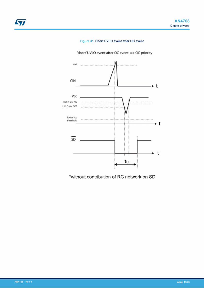
Figure 31. Short UVLO event after OC event
*without contribution of RC network on SD
AN4768IC gate drivers
AN4768 - Rev 4 page 34/78

Figure 32. Long UVLO event after OC event
AN4768IC gate drivers
AN4768 - Rev 4 page 35/78
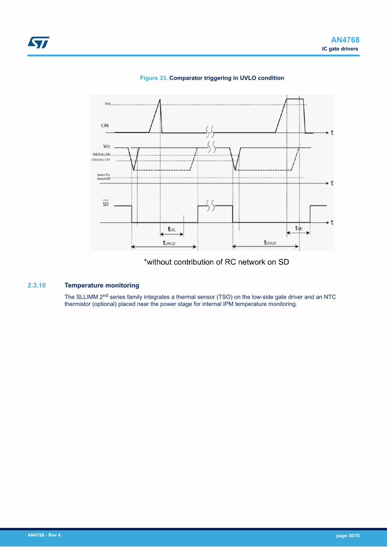
Figure 33. Comparator triggering in UVLO condition
2.3.10 Temperature monitoringThe SLLIMM 2nd series family integrates a thermal sensor (TSO) on the low-side gate driver and an NTCthermistor (optional) placed near the power stage for internal IPM temperature monitoring.
AN4768IC gate drivers
AN4768 - Rev 4 page 36/78

Figure 34. Temperature detection points (top view)
Thermal Sensor TSO
NTC thermistor (when available)
2.3.10.1 Thermal sensor (TSO)
The SLLIMM 2nd series family includes a temperature sensor integrated on the LS gate driver. The internal heatgenerated during normal operation is transferred to the sensor through the internal resin and heatsink.Temperature and consequent voltage variation is therefore not immediate. For this reason, we recommend usingthis function for monitoring and eventual protection when slow temperature increases are detected in cases suchas during continuous overload. A voltage proportional to the temperature is available on TSO pin (17) and thesensor does not need any pull down resistor. To increase the noise immunity, a capacitor filter of 1 to 10 nF mustbe placed on this pin.This function cannot shut the SLLIMM down directly if the temperature rises above safe temperatures, but theoutput voltage can be sent to a circuit (such as a comparator) to provide feedback to the MCU which can in turnhalt the IPM.The figure below shows a typical voltage variation with temperature graph. For specific device information, pleaserefer to the relevant datasheet.
AN4768IC gate drivers
AN4768 - Rev 4 page 37/78
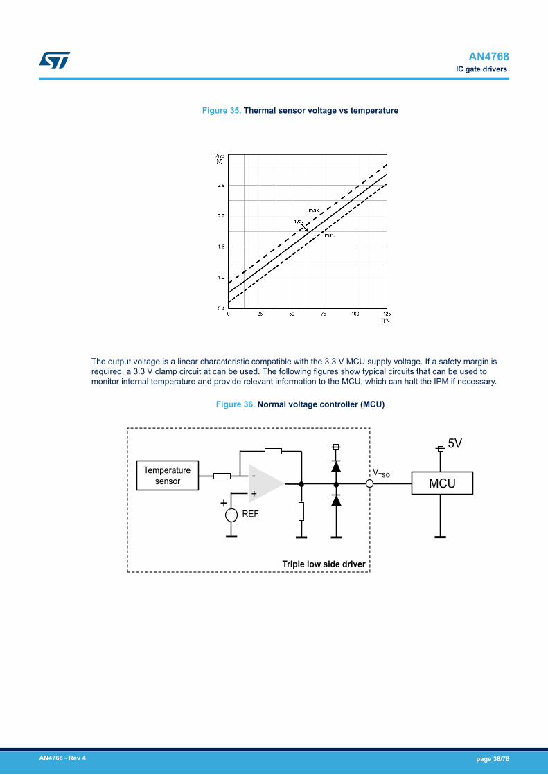
Figure 35. Thermal sensor voltage vs temperature
The output voltage is a linear characteristic compatible with the 3.3 V MCU supply voltage. If a safety margin isrequired, a 3.3 V clamp circuit at can be used. The following figures show typical circuits that can be used tomonitor internal temperature and provide relevant information to the MCU, which can halt the IPM if necessary.
Figure 36. Normal voltage controller (MCU)
REF
-++
Temperature sensor
VTSO
Triple low side driver
MCU
5V
AN4768IC gate drivers
AN4768 - Rev 4 page 38/78

Figure 37. Low voltage controller (MCU): optional clamping
REF
-++
Temperature sensor
VTSO
Triple low side driver
MCU
3.3V
The internal circuit consists of a temperature sensor, an amplification network to amplify the signal and ESDprotection. Its current capability is 4 mA min. source (ITSO_SRC) and 0.1 mA typ. (ITSO_SNK).When this function is not used, the TSO pin can be left floating.
2.3.10.2 NTC Thermistor
The SLLIMM 2nd series can be optionally equipped with a negative temperature coefficient (NTC) thermistor foreasy over temperature protection, by sending the microcontroller real-time temperature data.Due to the thermal impedance of SLLIMM and its own time constant, the NTC thermistor is not suited to detectingrapid junction temperature rises directly in the power devices. Therefore, it cannot be used for short-circuit orovercurrent protection, but only to monitor gradual changes in temperature.The NTC thermistor is placed very close to the power stage for accurate junction temperature monitoring of powerchips.The resistance versus temperature characteristic of NTC thermistor is non-linear and it is described by thefollowing expression:Equation 11 R T = R25 ∙ eB 1T − 1298Where T is the temperature in Kelvin, B is a constant in the SLLIMM operating range and R25 is the resistance at25 °C; these last two parameters are shown in the datasheet.The built-in thermistor (85 kΩ at 25 °C) is inside the IPM and connected between T1 and T2 pins (26, 25).
AN4768IC gate drivers
AN4768 - Rev 4 page 39/78

Figure 38. NTC resistance vs temperature
Figure 39. NTC resistance vs temperature – zoom
The following figure shows a simple circuit using a voltage divider for both overtemperature protection andtemperature monitoring.
AN4768IC gate drivers
AN4768 - Rev 4 page 40/78

Figure 40. Sample overtemperature protection circuit
T1
T2
+VDD
NTC
SLLIMM
COT ROT
SD
VNTC_th
+
-
The external comparator is used to send a shutdown signal to the SLLIMM in case of over temperature. VNTC_th isa threshold voltage, fixed by design, and connected to the non-inverting input, while the inverting input isconnected to a voltage divider based on the NTC and ROT resistors. When the voltage on the inverting inputexceeds the VNTC_th value, the comparator triggers, pulling down the SD pin and consequently switching off theLS IGBTs.For a proper sizing of the voltage divider, the maximum allowed temperature level (TOT_Max) must first be set andthe thermistor resistance derived from Equation 11, as well as from Figure 38. NTC resistance vs temperature andFigure 39. NTC resistance vs temperature – zoom. The value of resistance ROT can be calculated with thevoltage divider formula:Equation 12 V− T = ROTRNTC T + ROT ∙ VDDconsidering that, if T = TOT_Max then V-(TOT_Max) = VNTC_th.The maximum allowed power on the thermistor should not exceed 5 mW across the entire operating range inorder to guarantee safe operation and avoid power consumption affecting the temperature measurement throughself-heating.Therefore, for T = TOT_Max:Equation 13 RNTC ∙ I2 = RNTC ∙ VDDRNTC+ROT 2 ≤ 5mWFinally, to increase the noise immunity of the NTC thermistor, we recommend placing a decoupling capacitor(COT) in parallel, whose value must be between 10 and 100 nF.The following figures show two sample pull up and pull down resistor configurations and corresponding voltageoutput graphs as function of temperature. Both curves include the maximum spread according to the tolerance ofthe NTC and RPU / RPD resistances.
AN4768IC gate drivers
AN4768 - Rev 4 page 41/78

Figure 41. VNTC vs temperature (pull up configuration)
Figure 42. VNTC vs temperature (pull down configuration)
2.3.11 Bootstrap circuitIn the 3-phase inverter, the emitters of the low-side IGBTs are connected to the negative DC bus (VDC-) as thecommon reference ground, which allows all low-side gate drivers to share the same power supply, while theemitter of the high-side IGBTs is alternately connected to the positive (VDC+) and negative (VDC-) DC bus duringoperation.
AN4768IC gate drivers
AN4768 - Rev 4 page 42/78

A bootstrap method is a simple and cheap solution to supply the high voltage section. This function is normallyaccomplished by a high voltage fast recovery diode.The SLLIMM family includes a patented integrated structure that replaces the external diode. It is realized with ahigh voltage DMOS working as a diode with a series resistor.The new bootstrap diode structure used in the 2nd series offers further benefits compared to previous series. As itis no longer synchronized with its low-side input signal, the bootstrap capacitor can be recharged regardless ofwhich LS IGBT is on and even during the low-side freewheeling recirculation phase. This avoids using theexternal bootstrap diode even in non-complementary switching schemes such as the 6-step modulation.The operation of the bootstrap circuit is shown in the figure below. The floating supply capacitor CBOOT is chargedby the VCC supply when VOUT is lower than VCC through the bootstrap diode and the DMOS path with referenceto the “bootstrap charge current path”. During the high-side IGBT on phase, the bootstrap circuit provides the rightgate voltage to properly drive the IGBT (see “bootstrap discharge current path”). This circuit is iterated for all thethree half-bridges.
Figure 43. Bootstrap circuit
OUT
HVG
Vboot
P
N
U, V, W
DMOS
Vboot
VCCH
LINu,v,w
OUT
VCC
SLLIMM
bootstrapdiode
+
Legend:Bootstrap charge current pathBootstrap discharge current path
Triple high side driver
LVGGND
Triple low side driver
VCC
HINu,v,w
GND
GND
VCCL
CIN
The value of the CBOOT capacitor should be calculated according to the application condition and must take thefollowing into account:
AN4768IC gate drivers
AN4768 - Rev 4 page 43/78

• The voltage across CBOOT must be maintained at a value higher than the undervoltage lockout level(VBS_th). This enables the high-side IGBT to work with the correct gate voltage (lower dissipation and betteroverall performances).
• The voltage across CBOOT is affected by different components such as drops across the integratedbootstrap structure, drops across the low-side IGBT, and others.
• When the high-side IGBT is on, the CBOOT capacitor discharges mainly to provide the right IGBT gatecharge, but other phenomena must be considered such as leakage currents, quiescent current, etc.
• Bear in mind that if a voltage below the UVLO threshold is applied on the bootstrap channel, the HS gatedriver disables its output without a fault signal.
2.3.11.1 Bootstrap capacitor selection
A simple method to properly size the bootstrap capacitor involves considering only the amount of charge that isneeded when the high voltage side of the driver is floating and the IGBT gate is driven once. This approach takesneither the duty cycle of the PWM nor the fundamental frequency of the current into account. Observationsregarding the PWM duty cycle, kind of modulation (6-step, 12-step and sine-wave) must be considered accordingto their individual specifics to achieve best bootstrap circuit sizing.During the bootstrap capacitor charging phase, the low-side IGBT is on and the voltage across CBOOT (VCBOOT)can be calculated as follows:Equation 14 VCBOOT = VCC − VF − VDS on − VCE sat maxWhere:• VCC: supply voltage of gate driver• VF: bootstrap diode forward voltage drop• VCE(sat)max: maximum emitter collector voltage drop of low-side IGBT• VDS(on): DMOS driving voltage drop
The magnitude of the bootstrap capacitance CBOOT value is based on the minimum voltage drop (ΔVCBOOT) toguarantee when the high-side IGBT is on, and must be:Equation 15 ΔVCBOOT = VCC − VF − VDS on − VGE min − VCE sat maxUnder the condition:Equation 16 VBOOT min > VBS_tℎONWhere:• VGE(min): minimum gate emitter voltage of high-side IGBT• VBS_thON: bootstrap turn on undervoltage threshold (maximum value, see datasheet).
Considering the factors contributing to VCBOOT decreasing, the total charge supplied by the bootstrap capacitor(during high-side on phase) is:Equation 17 QTOT = QGATE+ ILKGE+ IQBO+ ILK+ ILKDiode+ ILKCap ∙ tHon+ QLSWhere:• QGATE: total IGBT gate charge• ILKGE: IGBT gate emitter leakage current• IQBO: bootstrap circuit quiescent current• ILK: bootstrap circuit leakage current• ILKDiode: bootstrap diode leakage current• ILKCap: bootstrap capacitor leakage current (relevant when using an electrolytic capacitor but can be ignored
if other types of capacitors are used)• tHon: high-side on time• QLS: charge required by the internal level shifters
AN4768IC gate drivers
AN4768 - Rev 4 page 44/78

Finally, the minimum size of the bootstrap capacitor is:Equation 18 CBOOT = QTOT∆VCBOOTTo aid in the selection of the bootstrap capacitor, the figure below shows the behavior of CBOOT (calculated)versus switching frequency (fsw), with different values of ΔVCBOOT, corresponding to Equation 18 for a continuoussinusoidal modulation and for STGIB30M60xy-z(worst case) and a duty cycle δ = 50%. For all the other devices,the bootstrap capacitor can be calculated using the same curve.
Figure 44. Bootstrap capacitor vs. switching frequency
0
1
2
3
4
0 5 10 15 20
CB
OO
T C
alcu
late
d (u
F)
fsw (kHz)
STGIB30M60d=50%
DVCBOOT= 0.1V
DVCBOOT= 0.3V
DVCBOOT= 0.5V
Considering the extreme cases during PWM control and further leakage and dispersion in the board layout, thecapacitance value for the bootstrap circuit should be two or three times higher than CBOOT derived from Figure44. Bootstrap capacitor vs. switching frequency. The bootstrap capacitor should have a low ESR value for goodlocal decoupling; therefore, if an electrolytic capacitor is used, a parallel ceramic capacitor placed directly on theSLLIMM pins is highly recommended.
2.3.11.2 Initial bootstrap capacitor charging
During the startup phase, the bootstrap capacitor must be charged long enough to complete the initial chargingtime (tCHARGE), which is at least the time VCBOOT needs to exceed the turn-on undervoltage threshold VBS_thON,as already stated in Equation 14.For normal operation, the voltage across the bootstrap capacitor must never drop down to the turn-offundervoltage threshold VBS_thOFF.During startup, only the low-side IGBT is switched on and the PWM is run immediately after tgis phase, as shownby the sequence in the following figure.
AN4768IC gate drivers
AN4768 - Rev 4 page 45/78

Figure 45. Initial bootstrap charging time
Time
VCBOOT
t1
LVG
VCC
DC Bus VPN
VBS_thON
t3t2
HVG
VBS_thOFF
The timing chart is based on the following steps:• t1: the bootstrap capacitor starts to charge through the low-side IGBT (LVG)• t2: the voltage across the bootstrap capacitor (VCBOOT) reaches its turn-on undervoltage threshold VBS_thON
• t3: the bootstrap capacitor is fully charged, this enables the high-side IGBT and the CBOOT capacitor startsdischarging in order to provide the right IGBT gate charge. The bootstrap capacitor recharges during the onstate of the low-side IGBT (LVG).
The initial charging time is given by Equation 19 and must, for safety reasons, be at least three times longer thanthe calculated value.Equation 19 tCHARGE ≥ CBOOT ∙ RDS onδ ∙ ln VCC∆VCBOOTWhere δ is the duty cycle of the PWM signal and RDS(on) is 150 Ω typical value, as per the datasheet.A practical example can be analyzed by considering a motor drive application where the PWM switchingfrequency is 12.5 kHz, with a duty cycle of 50%, and ΔVCBOOT = 0.1 V (hence a gate driver supply voltageVCC = 17.6 V). From the graph in Figure 44. Bootstrap capacitor vs. switching frequency, the bootstrapcapacitance is 1.5 µF so CBOOT can be chosen between 3.0 and 4.5 µF. We shall adopt the commerciallyavailable 3.3 µF capacitor.From Equation 19, the initial charging time is:Equation 20 tCHARGE ≥ 3.3 ∙ 10−6 ∙ 1500.5 ∙ ln 17.60.1 = 5 msFor safety reasons, the initial charging time must be at least 15 ms.
2.3.12 Output safe clampBoth HS and LS gate driver ICs are designed with an output safe clamp to guarantee the low impedance of theIGBT driving network (VLVG, VHVG = 1V @ Isink = 10 mA, VCC > 3 V) even in the shutdown condition. This featureguarantees the off state of the IGBT and avoids any undesired turning on due to the Miller effect, for example.
AN4768IC gate drivers
AN4768 - Rev 4 page 46/78

3 Package
The SLLIMM 2nd series benefits from a more compact package while providing high power density, the bestthermal performance, and good electrical isolation (>1500 VRMS).The SDIP2x-26L is a dual-in-line transfer mold package available in two technology options: full molded type foran optimized cost/performance tradeoff and DBC (Direct Bonded Copper) type for best performance.Both package technologies have the same physical size and are available in 26-lead versions (SDIP2F-26L,SDIP2B-26L) with or without an additional on board NTC thermistor. A vacuum soldering process is used to avoidthe inclusion of any gas (voids) during the soldering process that could cause potential hot spots. This results in afurther increase in the reliability of the SLLIMM family due to the improved thermal and electrical conductivity.The full molded technology is oriented towards cost effectiveness and represents an ideal choice for low/mediumpower platforms.The DBC technology allows extremely low thermal resistance values, high stability in thermal cycling and highquality.All the versions are also available in two different configurations as short leads with emitter forward (suffix -E) andlog leads (suffix -L).
3.1 Full molded structureThe full molded package consists of a copper lead frame with power stage and control stage soldered on it andhoused using the transfer molding process. The excellent thermal properties of the copper allows good heatspread and heat transfer, furthermore, the thickness of transfer mold resin and the layout of the lead frames hasbeen optimized in order to further reduce the thermal resistance, while providing targeted electrical isolation leveland overall reliable performance.
3.2 DBC structureDBC stands for direct bonded copper, a process in which copper and a ceramic material are directly bonded, asshown in the figure below. Direct bonded copper substrates are a proven, high performance solution for theelectrical isolation and thermal management of high power semiconductor modules.
Figure 46. DBC structure
The advantages of DBC substrates are:• high current-carrying capability, due to thick copper metallization• a thermal expansion coefficient close to the silicon value at the copper surface.
DBC has two layers of copper that are directly bonded onto an aluminum-oxide (Al2O3) ceramic base. The DBCprocess yields a super-thin base and eliminates the need for the thick, heavy copper bases used prior to thisprocess.Because SLLIMM with DBC bases has fewer layers, it has much lower thermal resistance values than those onebased on different materials.The main properties of DBC include:• high mechanical strength• mechanically stable dimensions
AN4768Package
AN4768 - Rev 4 page 47/78

• good adhesion• corrosion resistance• excellent electrical isolation• high thermal conductivity• a thermal expansion coefficient similar to that of the silicon, so no interface layers are required• good heat diffusion• can be structured just like printed circuit boards or "IMS substrates"• environmentally friendly
The DBC package consists of a DBC substrate for the power stage and a lead frame structure for the controlstage, both housed using the transfer molding process.Thanks to the new DBC substrate enhancement, the new SLLIMM 2nd series shows significant thermal resistancereduction up to 20% less than the SLLIMM 1st series. The following figure and corresponding table show an Rthcomparison of SLLIMM 2nd series in DBC and full molded packages, and SLLIMM 1st series available only inDBC.
Figure 47. Thermal resistance comparison
5.5
5
4.5
4
3.5
3
2.5
2
1.510 5 10 15 20 25 30
RTHjc(°C/W)
ICN(A) at 25°C
2ndserie s - full molded
2nd series - full molded
1st series - DBC
2nd series - DBC
Table 12. Rth(j-c) comparison
PN SLLIMM series ICNRTH(J-C)
IGBT
STGIF5CH60x
2nd
FM
8 A 5.0 °C/W
STGIF7CH60x 10 A 4.8 °C/W
STGIF10CH60x 15 A 4.6 °C/W
STGIB8CH60x
DBC
12 A 3.0 °C/W
STGIB10CH60x 15 A 2.26 °C/W
STGIB15CH60x 20 A 1.85 °C/W
STGIB20M60x 25 A 1.40 °C/W
STGIB30M60x 35 A 1.20 °C/W
AN4768DBC structure
AN4768 - Rev 4 page 48/78
PN SLLIMM series ICNRTH(J-C)
IGBT
STGIPS10K60
1st DBC
10 A 3.8 °C/W
STGIPS14K60 14 A 3 °C/W
STGIPS20K60 18 A 2.4 °C/W
STGIPL20K60 20 A 2.2 °C/W
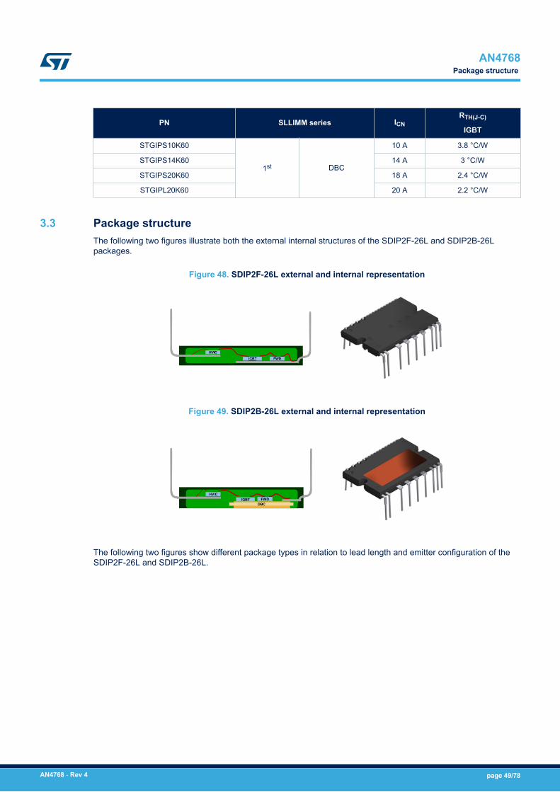
3.3 Package structureThe following two figures illustrate both the external internal structures of the SDIP2F-26L and SDIP2B-26Lpackages.
Figure 48. SDIP2F-26L external and internal representation
Figure 49. SDIP2B-26L external and internal representation
The following two figures show different package types in relation to lead length and emitter configuration of theSDIP2F-26L and SDIP2B-26L.
AN4768Package structure
AN4768 - Rev 4 page 49/78

Figure 50. SDIP2F-26L and SDIP2B-26L – short leads and emitter forward package
AN4768Package structure
AN4768 - Rev 4 page 50/78

Figure 51. SDIP2F-26L and SDIP2B-26L – long leads package
For further package outline details and dimensions, refer to the relevant datasheet.
3.4 Input and output pin descriptionsThis section defines the SLLIMM 2nd series input and output pins. For a more accurate description and layoutsuggestions, please consult the relevant sections.
Table 13. SDIP2x-25/26L input and output pins
Pin Name Description
1 - NC
2 VBOOTu bootstrap voltage for U phase
3 VBOOTv bootstrap voltage for V phase
4 VBOOTw bootstrap voltage for W phase
5 HINu high-side logic input for U phase
6 HINv high-side logic input for V phase
7 HINw high-side logic input for W phase
8 VCCH high-side low voltage power supply
9 GND Ground
10 LINu low-side logic input for U phase
AN4768Input and output pin descriptions
AN4768 - Rev 4 page 51/78
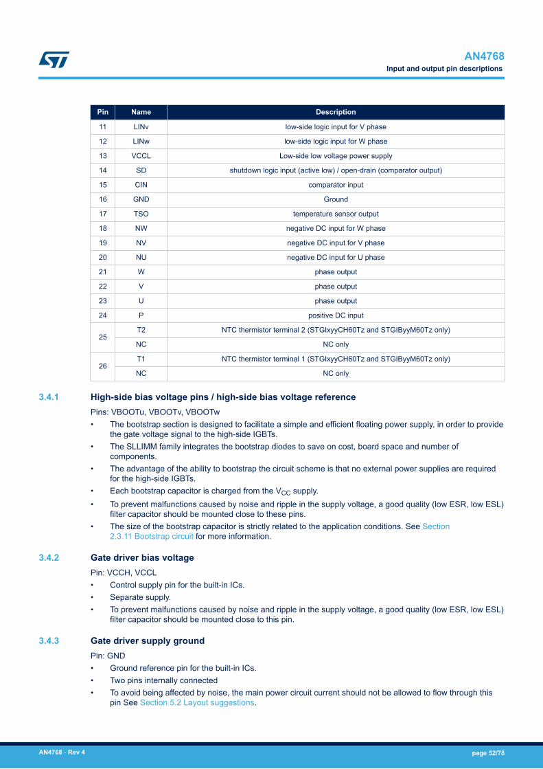
Pin Name Description
11 LINv low-side logic input for V phase
12 LINw low-side logic input for W phase
13 VCCL Low-side low voltage power supply
14 SD shutdown logic input (active low) / open-drain (comparator output)
15 CIN comparator input
16 GND Ground
17 TSO temperature sensor output
18 NW negative DC input for W phase
19 NV negative DC input for V phase
20 NU negative DC input for U phase
21 W phase output
22 V phase output
23 U phase output
24 P positive DC input
25T2 NTC thermistor terminal 2 (STGIxyyCH60Tz and STGIByyM60Tz only)
NC NC only
26T1 NTC thermistor terminal 1 (STGIxyyCH60Tz and STGIByyM60Tz only)
NC NC only
3.4.1 High-side bias voltage pins / high-side bias voltage referencePins: VBOOTu, VBOOTv, VBOOTw• The bootstrap section is designed to facilitate a simple and efficient floating power supply, in order to provide
the gate voltage signal to the high-side IGBTs.• The SLLIMM family integrates the bootstrap diodes to save on cost, board space and number of
components.• The advantage of the ability to bootstrap the circuit scheme is that no external power supplies are required
for the high-side IGBTs.• Each bootstrap capacitor is charged from the VCC supply.• To prevent malfunctions caused by noise and ripple in the supply voltage, a good quality (low ESR, low ESL)
filter capacitor should be mounted close to these pins.• The size of the bootstrap capacitor is strictly related to the application conditions. See Section
2.3.11 Bootstrap circuit for more information.
3.4.2 Gate driver bias voltagePin: VCCH, VCCL• Control supply pin for the built-in ICs.• Separate supply.• To prevent malfunctions caused by noise and ripple in the supply voltage, a good quality (low ESR, low ESL)
filter capacitor should be mounted close to this pin.
3.4.3 Gate driver supply groundPin: GND• Ground reference pin for the built-in ICs.• Two pins internally connected• To avoid being affected by noise, the main power circuit current should not be allowed to flow through this
pin See Section 5.2 Layout suggestions.
AN4768Input and output pin descriptions
AN4768 - Rev 4 page 52/78

3.4.4 Signal inputPins: HINU, HINV, HINW; LINU, LINV, LINW;• These pins control the operation of the built-in IGBTs.• The signal logic of HINU, HINV, HINW, LINU, LINV, and LINW pins is active high. The IGBT associated with
each of these pins is turned on when a sufficient logic (higher than a specific threshold) voltage is applied tothese pins.
• The wiring of each input should be as short as possible to protect the SLLIMM against noise.
3.4.5 Internal comparator non-invertingPin: CIN• The current sensing shunt resistor connected on each phase leg may be used by the internal comparator
(pin CIN) to detect short-circuit current.• The shunt resistor should be selected to meet the detection level requirements for the specific application.• An RC filter (typically ~1us) should be connected to the CIN pin to eliminate noise.• The connection length between the shunt resistor and CIN pin should be minimized.• If a voltage signal higher than the specified VREF (see datasheet) is applied to this pin, the SLLIMM
automatically shuts down and the SD / OD pin is pulled down (to inform the microcontroller).
3.4.6 Shutdown / open-drainPin: SD / OD• The SD / OD pin acts as an enable/disable pin.• The signal logic of the SD / OD pin is active low. The SLLIMM shuts down if a voltage lower than a specific
threshold is applied to this pin, leading each half bridge in tri-state.• The SD / OD status is also connected to the internal comparator status (Section 2.3.5 Short-circuit protection
and smart shutdown function). When the comparator triggers, the SD / OD pin is pulled down and acts as aFAULT pin.
• When pulled down by the comparator, the SD / OD pin is open drain configured. The SD / OD voltage shouldbe pulled up to the 3.3 V or 5 V logic power supply through a pull-up resistor.
3.4.7 ThermistorPins: T1, T2• A co-packaged NTC (optional) is available for temperature monitoring purposes.• A simple voltage divider can be made with an external resistor in order to create a temperature-dependent
voltage signal.• The NTC is not able to sense rapid variations in IGBT junction temperature (due to the slow thermal
dynamics).
3.4.8 Thermal sensorPin: TSO• A voltage proportional to the temperature inside the package is available on the TSO pin. It does not need
any pull down resistor. To improve noise immunity, a capacitor filter between 1 and 10 nF should be placedon this pin. When this function is not used, the TSO pin can be left floating.
3.4.9 Positive DC-linkPin: P• This is the DC-link positive power supply pin of the inverter and is internally connected to the collectors of
the high-side IGBTs.• To suppress the surge voltage caused by the DC-link wiring or PCB pattern inductance, connect a snubber
capacitor close to this pin (typically, high voltage, metal film capacitors of about 0.1 or 0.22 μF).
3.4.10 Negative DC-linkPins: NU, NV, NW
AN4768Input and output pin descriptions
AN4768 - Rev 4 page 53/78

• These are the DC-link negative power supply pins (power ground) of the inverter.• These pins are connected to the low-side IGBT emitters of each phase.• The power ground of the application should be separated from the logic ground of the system and
reconnected at one specific point (star connection).
3.4.11 Inverter Power OutputPins: U, V, W• Inverter output pins for connection to the inverter load (e.g., motors).
AN4768Input and output pin descriptions
AN4768 - Rev 4 page 54/78

4 Power loss and dissipation
The total power loss in an inverter derives from conduction losses, switching losses and off-state losses and isessentially generated by the power devices of the inverter stage, such as the IGBTs and the freewheeling diodes.The conduction losses (Pcond) are the on-state losses generated during the conduction phase. The switchinglosses (Psw) are the dynamic losses encountered during turn-on and turn-off. Off-state losses deriving fromblocking voltage and leakage current can be ignored.Total power loss is given by:Equation 21 Ptot ≈ Pcond+ PswThe figure below shows a typical waveform and the major sources of power loss of an inductive hard switchingapplication such as a motor drive.
Figure 52. Typical IGBT power losses
VCE IC
10% IC 10% VCE 10% VCE 10% IC
Esw(on)Esw(off)
VCE(sat)
tc(on) tc(off)conduction
4.1 Conduction power lossesConduction losses are caused by IGBT and freewheeling diode forward voltage drops at rated currents. They canbe calculated using a linear approximation of the forward characteristics for both IGBT and diode, in a seriesconnection with a DC voltage source representing the threshold voltage, VTO for IGBT, (and VFO for diode) and acollector emitter on-state resistance, RCE (and RAK anode cathode on-state resistance), as shown in the figurebelow for reference purposes.
AN4768Power loss and dissipation
AN4768 - Rev 4 page 55/78

Figure 53. IGBT and diode approximate output characteristics
Both forward characteristics are temperature dependent, and so must be considered with respect to a specifictemperature.The linear approximations for IGBTs can be translated into the following equation:Equation 22 vce ic = VTO+ RCE ∙ ic...and for freewheeling diodes:Equation 23 vfm ifm = VFO+ RAK ∙ ifmThe conduction losses of IGBT and diode can be derived as the time integral of the product of conduction currentand voltage across the devices, as such:Equation 24 Pcond_IGBT = 1T∫0Tvce ∙ ic t dt = 1T∫0T VTO ∙ ic t + Rce+ ic2 t dtEquation 25 Pcond_DIODE = 1T∫0Tvf ∙ if t dt = 1T∫0T VFO ∙ if t + RAK+ if2 t dtWhere T is the fundamental period.As differing SLLIMM utilization modes, modulation techniques and operating conditions complicate power lossestimation, it is necessary to set some initial conditions.Assuming that:• the application is a variable voltage variable frequency (VVVF) inverter based on sinusoidal PWM technique.• the switching frequency is high and therefore the output currents are sinusoidal• the load is ideal inductive
Under these conditions, the output inverter current is given by:Equation 26 i = Îcos θ − ϕWhere Î is the current peak, θ represents ωt and ф is the phase angle between output voltage and current.The conduction power losses can be obtained from:Equation 27
Pcond_IGBT = VTO ∙ Î2π ∫−π2 + ϕπ2 + ϕ ξcos θ − ϕ dθ+ RCE ∙ Î2π ∫−π2 + ϕπ2 + ϕ ξcos2 θ − ϕ dθ
AN4768Conduction power losses
AN4768 - Rev 4 page 56/78

Equation 28
Pcond_DIODE = VFO ∙ Î2π ∫−π2 + ϕπ2 + ϕ 1− ξ cos θ − ϕ dθ+ RAK ∙ Î22π ∫−π2 + ϕπ2 + ϕ 1− ξ cos2 θ − ϕ dθWhere ξ is the duty cycle for this PWM technique given by:Equation 29 ξ = 1 +ma ∙ cosθ2Where ma is the PWM amplitude modulation index.Finally, solving for Equation 27 and Equation 28, we obtain:Equation 30 Pcond_IGBT = VTO ∙ Î 12π + ma ∙ cosϕ8 + RCE ∙ Î2 18 + ma ∙ cosϕ3πEquation 31 Pcond_DIODE = VFO ∙ Î 12π − ma ∙ cosϕ8 + RAK ∙ Î2 18 − ma ∙ cosϕ3πand therefore, the conduction power loss for a single device (IGBT and diode) is:Equation 32 Pcond = Pcond_IGBT+ Pcond_DIODEOf course, the total conduction loss for an inverter is six times this value.
4.2 Switching power lossesThe switching loss is the power consumption during the turn-on and turn-off transients. As already shown inFigure 53. IGBT and diode approximate output characteristics, it is given by the pulse of power dissipated duringturn-on (ton) and turn-off (toff).Experimentally, it can be calculated by the time integral of the product of the collector current and collector-emittervoltage for the switching period. In any case, the dynamic performance is heavily dependent on severalparameters including voltage, current temperature, so it is necessary to employ the same assumptions in Section4.1 Conduction power losses to simplify the calculations.Under these conditions, the switching energy losses are given by:Equation 33 Eon θ = Êoncos θ − ϕEquation 34 Eoff θ = Êoffcos θ − ϕWhere Êon and Êoff are the maximum values taken at Tjmax and ÎC, θ equals ωt and ф is the phase anglebetween output voltage and current.Finally, the switching power loss per device depends on the switching frequency (fsw) and is calculated as follows:Equation 35
Psw = 12π∫−π2 + ϕπ2 + ϕ EIGBT+ EDiode ∙ fswdθ = EIGBT+ EDiode ∙ fswπWhere EIGBT and EDiode are the total switching energy for IGBT and freewheeling diode, respectively. Also in thiscase, the total switching loss per inverter is six times this value.The figure below shows the real turn-on and turn-off waveforms of STGIF5CH60xy-z under the followingconditions:VPN = 300 V, IC = 5 A, Tj = 150 °C with inductive load on full bridge topology, taken on the low-side IGBT.The light blue plots represent instantaneous power as the product of IC (in green) and VCE (in red) waveformsduring the switching transitions. The areas under these plots are the switching energies computed by graphicintegration thanks to the digital oscilloscope.
AN4768Switching power losses
AN4768 - Rev 4 page 57/78

Figure 54. STGIF5CH60xy-x typical switching waveforms
4.3 Thermal impedance overviewDuring operation, power losses generate heat which elevates the temperature in the internal SLLIMMsemiconductor junctions, limiting its performance and lifetime. To ensure safe and reliable operation, the junctiontemperature of power devices must be kept below the limits defined in the datasheet, therefore, the generatedheat must be conducted away from the power chips and into the environment using an adequate cooling system.The most common schemes are based on one heatsink designed for free conventional air flow or, in some cases,for forced air circulation. Free conventional air flow systems require larger heatsinks (about 50% bigger) than aforced air based heatsink, for a given thermal resistance. Therefore, the choice of the cooling system becomesthe starting point for the application designer and the thermal aspect of the system is one of the key factors indesigning high efficiency and high reliability equipment. In this respect, the package and its thermal resistanceplay a fundamental role.Thermal resistance quantifies the ability of a given thermal path to transfer heat in the steady-state and isgenerally expressed as the ratio between the temperature increase above the reference and the relevant powerflow:Equation 36 Rtℎ = ∆T∆PThe thermal resistance specified in the datasheet is the junction-case Rth(j-c), defined as the temperaturedifference between the junction and case reference divided by the power dissipation per device:Equation 37 Rtℎ j − c = Tj − TcPDThe SLLIMM 2nd series (DBC package) benefits from a state of the art DBC substrate offering a very low Rth(j-c)value. The backside of the DBC substrate and the full molded package are used as the cooling interface to theheatsink.Thermal grease or some other thermal interface material between the backside and the heatsink is used toreduce the thermal resistance of the interface (Rth(c-h)) and, of course, depends on the material and its thickness.Basically, the sum of the three thermal resistance components above gives the thermal resistance betweenjunction and ambient Rth(j-a), as shown in the figure below.
AN4768Thermal impedance overview
AN4768 - Rev 4 page 58/78
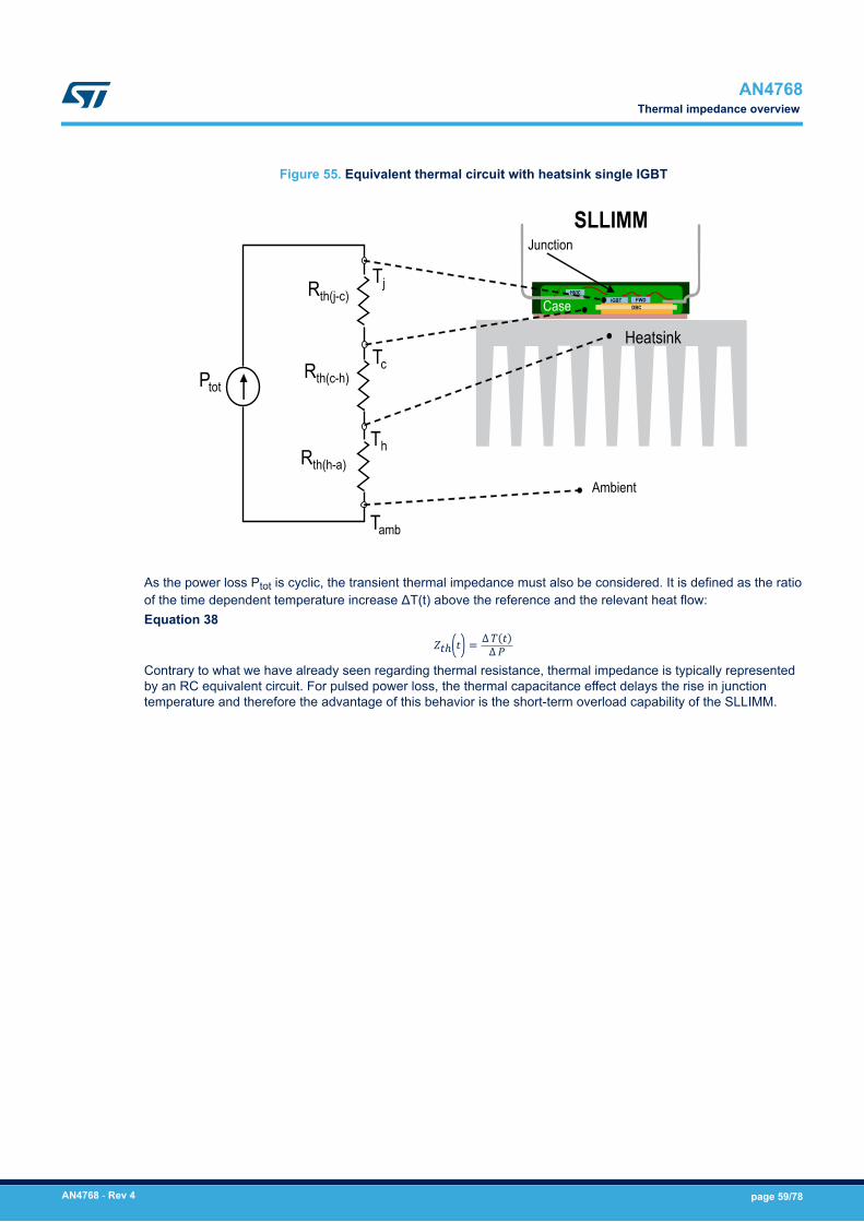
Figure 55. Equivalent thermal circuit with heatsink single IGBT
As the power loss Ptot is cyclic, the transient thermal impedance must also be considered. It is defined as the ratioof the time dependent temperature increase ΔT(t) above the reference and the relevant heat flow:Equation 38 Ztℎ t = ∆T t∆PContrary to what we have already seen regarding thermal resistance, thermal impedance is typically representedby an RC equivalent circuit. For pulsed power loss, the thermal capacitance effect delays the rise in junctiontemperature and therefore the advantage of this behavior is the short-term overload capability of the SLLIMM.
AN4768Thermal impedance overview
AN4768 - Rev 4 page 59/78

Figure 56. Thermal impedance curves
0
1
2
3
4
5
6ZT
Hjc [
°C/W
]
time [s]
STGIF5CH60xy-z STGIF7CH60xy-z STGIF10CH60xy-z STGIB8CH60xy-z
STGIB10CH60xy-z STGIB15CH60xy-z STGIB20M60xy-z STGIB30M60xy-z
STGIF5CH60xy-z
STGIF7CH60xy-z
STGIF10CH60xy-z
STGIB8CH60xy-z
STGIB10CH60xy-z
STGIB15CH60xy-z
STGIB20M60xy-z
STGIB30M60xy-z
More generally, in the case of the device, power is time dependent too. The device temperature can be calculatedvia the convolution integral method applied to the following equation thus:Equation 39 ∆T t = ∫0tZth t − τ ∙ P τ dτAn alternative and very useful method for simulator tools, is the transient thermal impedance model, whichprovides a simple method for estimating the junction temperature rise under a transient condition.By using the thermo-electrical analogy, the transient thermal impedance Zth(t) can be transformed into anelectrical equivalent RC network. The number of RC sections increases the model detail, therefore a fourth ordermodel based on the Cauer network has been adopted to improve the accuracy of the model, as shown in thefigure below.
Figure 57. Thermal impedance RC Cauer thermal network
Tj
Ptot(t) C1 C2 C3 C4
R1 R2 R4R3
Tcase
Zth(t)
Temperatures inside the electrical RC network represent voltages, power flows represent currents, electricalresistances and capacitances represent thermal resistances and capacitances respectively. The casetemperature is represented with a DC voltage source and can be interpreted as the initial junction temperature.
AN4768Thermal impedance overview
AN4768 - Rev 4 page 60/78

Transient thermal impedance models are derived by curve fitting an equation to the measured data. Values for theindividual resistors and capacitors are the variables from this equation and are defined for each device in the tablebelow.
Table 14. RC Cauer thermal network elements by device
Element STGIF5CH60 STGIF7CH60 STGIF10CH60 STGIB8CH60 STGIB10CH60 STGIB15CH60 STGIB20M60 STGIB30M60
R1 (°C/W) 0.11 0.15 0.11 0.125 0.097 0.07112 0.055 0.048
R2 (°C/W) 0.55 0.55 0.50 0.315 0.24 0.1752 0.149 0.110
R3 (°C/W) 2.8 2.2 2.09 1.196 1.04 0.824 0.526 0.447
R4 (°C/W) 1.54 1.9 1.90 1.365 0.878 0.7696 0.643 0.571
C1 (W·s/°C) 1.50E-04 2.20E-04 3.50E-04 1.05E-04 2.46E-04 3.93E-04 4.06E-04 5.54E-04
C2 (W·s/°C) 1.70E-03 2.80E-03 2.80E-03 4.07E-04 8.79E-04 2.34E-03 3.63E-03 5.68E-03
C3 (W·s/°C) 1.60E-02 2.20E-02 2.20E-02 3.05E-03 5.86E-03 6.93E-03 1.08E-02 1.43E-02
C4 (W·s/°C) 5.10E-01 3.00E-01 2.00E-01 2.96E-02 4.85E-02 7.70E-01 6.89E-02 8.70E-02
4.4 Power loss calculation exampleFrom the power loss calculation and thermal aspects detailed in the previous sections, we can simulate themaximum IC(RMS) current versus switching frequency curves for an inverter using a 3-phase continuous PWMmodulation to synthesize sinusoidal output currents.The curves in Figure 58. Maximum IC(RMS) current vs. fsw simulated curves represent the maximum currentmanaged by the SLLIMM under safe conditions, when the junction temperature rises to 50 °C (maintaining a goodmargin from the 175 °C maximum junction temperature for SLLIMM 2nd) and the case temperature is 100 °C,which is a typical operating condition to guarantee the reliability of the system.These curves, functions of the motor drive typology and control scheme, are simulated under the conditionsreported in the figure below, with typical power loss.
Figure 58. Maximum IC(RMS) current vs. fsw simulated curves
AN4768Power loss calculation example
AN4768 - Rev 4 page 61/78
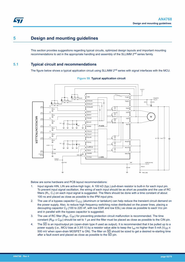
5 Design and mounting guidelines
This section provides suggestions regarding typical circuits, optimized design layouts and important mountingrecommendations to aid in the appropriate handling and assembly of the SLLIMM 2nd series family.
5.1 Typical circuit and recommendationsThe figure below shows a typical application circuit using SLLIMM 2nd series with signal interfaces with the MCU.
Figure 59. Typical application circuit
VTSO/NTC
Fault
Lin W
Lin V
Lin U
Hin W
Hin V
Hin U
VTSO/NTC
C3
C3
C3
CbootW
Cboot V
CbootU
R1
R1
R1
C1
C1
C1
R1
R1
R1
C1
C1
C1
(1)NC
(2)VbootU
(3)VbootV
(4)VbootW
(5)HinU
(6)HinV
(7)HinW
(8)VccH
(9)GNDC2
C2Vcc
Vc cCvc c
Cvcc
CTSO
CSD
RSDM
ICR
OC
ON
TRO
LLER
PWR_GND
to MCU/op-amp
CSF
RSF
Rshunt
C4 Cvdc
M
(10)LinU
(11)LinV
(12)LinW
(13)VccL
(14)SD/OD
(15)Cin
(16)GND
(17)TSO
NW(18)
NV(19)
NU(20)
W(21)
V(22)
U(23)
P(24)
T2(25)
T1(26)
L-side
H-side
CTORTO
3.3V/5 V
VTSO/NTC
Dz1
Dz1
Dz1
Dz2
Dz23.3V/5 V
SGN_GND
+
-
+
-
+
-
Below are some hardware and PCB layout recommendations:1. Input signals HIN, LIN are active-high logic. A 100 kΩ (typ.) pull-down resistor is built-in for each input pin.
To prevent input signal oscillation, the wiring of each input should be as short as possible and the use of RCfilters (R1, C1) on each input signal is suggested. The filters should be done with a time constant of about100 ns and placed as close as possible to the IPM input pins.
2. The use of a bypass capacitor CVCC (aluminum or tantalum) can help reduce the transient circuit demand onthe power supply. Also, to reduce high frequency switching noise distributed on the power lines, placing adecoupling capacitor C2 (100 to 220 nF, with low ESR and low ESL) as close as possible to each Vcc pinand in parallel with the bypass capacitor is suggested.
3. The use of RC filter (RSF, CSF) for preventing protection circuit malfunction is recommended. The timeconstant (RSF x CSF) should be set to 1 μs and the filter must be placed as close as possible to the CIN pin.
4. The SD is an input/output pin (open-drain type if used as output). It is recommended that it be pulled up to apower supply (i.e., MCU bias at 3.3/5 V) by a resistor value able to keep the Iod no higher than 5 mA (VOD ≤500 mV when open-drain MOSFET is ON). The filter on SD should be sized to get a desired re-starting timeafter a fault event and placed as close as possible to the SD pin.
AN4768Design and mounting guidelines
AN4768 - Rev 4 page 62/78

5. A decoupling capacitor CTSO between 1 nF and 10 nF can be used to increase the noise immunity of theTSO thermal sensor; a similar decoupling capacitor COT (between 10 nF and 100 nF) can be implemented ifthe NTC thermistor is available and used. In both cases, their effectiveness is improved if the capacitors areplaced close to the MCU.
6. The decoupling capacitor C3 (100 to 220 nF with low ESR and low ESL) in parallel with each Cboot is usefulto filter high frequency disturbances. Both Cboot and C3 (if present) should be placed as close as possible tothe U,V,W and Vboot pins. Bootstrap negative electrodes should be connected to U,V,W terminals directlyand separated from the main output wires.
7. To prevent overvoltage on the VCC pin, a Zener diode (Dz1) can be used. Similarly on the V boot pin, a Zenerdiode(Dz2) can be placed in parallel with each Cboot .
8. The use of the decoupling capacitor C4 (100 to 220 nF, with low ESR and low ESL) in parallel with theelectrolytic capacitor Cvdc is useful to prevent surge destruction. Both capacitors C4 and Cvdc should beplaced as close as possible to the IPM (C4 has priority over Cvdc).
9. By integrating an application-specific type HVIC inside the module, direct coupling to the MCU terminalswithout an opto-coupler is possible.
10. Low inductance shunt resistors should be used for phase leg current sensing.11. In order to avoid malfunction, the wiring between N pins, the shunt resistor and PWR_GND should be as
short as possible.12. The connection of SGN_GND to PWR_GND at only one point (close to the shunt resistor terminal) can help
to reduce the impact of power ground fluctuation.
5.2 Layout suggestionsPCB layout optimization for high voltage, high current and high switching frequency applications is a critical factor.PCB layout is a complex matter involving several aspects such as track length and width and circuit areas, butalso the proper routing of the traces and the optimized reciprocal arrangement of the various system elements inthe PCB area.A good layout can help the application function properly and achieve expected performance. On the other hand,PCBs without careful layout can generate EMI issues (both induced and perceived by the application), canprovide overvoltage spikes due to parasitic inductances along the PCB traces, and can produce higher power lossand even malfunction in the control and sensing stages.The compactness of the SLLIMM solution, which offers an optimized gate driving network and reduced parasiticelements, allows designers to concentrate on other issues such as the ground or noise filter. In any case, to avoidthe aforementioned conditions, the following general PCB layout guidelines and suggestions should be followedfor 3-phase applications.For more information please refer to application note AN4694.
5.3 General suggestions1. PCB traces should be designed as short as possible and the area of the circuit (power or signal) minimized
to reduce the sensitivity of such structures to surrounding noise.2. Ensure a good distance between switching lines with high voltage transitions and the signal lines sensitive to
electrical noise. Specifically, the tracks of each OUT phase carrying significant currents and voltages shouldbe separated from logic lines and analog op amp and comparator sensing circuits.
3. Place the RSENSE resistors as close as possible to the low-side pins of the SLLIMM (NU, NV and NW).Parasitic inductance can be minimized by connecting the ground line (also called driver ground) of theSLLIMM directly to the cold terminal of sense resistors. Use a low inductance type resistor, such as an SMDresistor instead of long-lead type resistors, to help further decrease parasitic inductance. The total parasiticinductance (including the shunt resistor) should be lower than 15 nH.
4. Avoid any ground loop. Only a single path must connect two different ground nodes.5. Place each RC filter as close as possible to the SLLIMM pins in order to increase their efficiency.6. Fixed voltage tracks such as GND or HV lines can be used to shield the logic and analog lines from
electrical noise produced by the switching lines (e.g., OUTu, OUTv and OUTw).
AN4768Layout suggestions
AN4768 - Rev 4 page 63/78

7. Generally, it is recommended to connect each half bridge ground in a star configuration and the threeRSENSE very close to each other and to the power ground.
8. In order to prevent surge destruction, the wiring between the snubber capacitor and the P N pins should beas short as possible. The use of a high frequency, high voltage non-inductive capacitor of about 0.1 or 0.22µF is recommended. In order to effectively suppress the surge voltage, the snubber capacitor has to beplaced in position (2) in Figure 60. Recommended snubber capacitor position. The position (1) is incorrectfor effective surge voltage suppression. If the capacitor is placed on the position (3), the charging anddischarging currents generated by wiring inductance and the snubber capacitor will appear on the shuntresistor with possible undesired protection activation, even if the surge suppression effect is the greatest.Finally, position (2) is the right compromise. The parasitic inductance on the A tracks (including that of theshunt resistor) should be as small as possible in order to suppress the surge voltage.
Figure 60. Recommended snubber capacitor position
(1) (3)(2)
P
Shunt resistorNVNW
+
-
Wiring inductance
NU
SLLIMM
(A)
The general suggestions for all SLLIMM products are summarized in the following figure.
Figure 61. PCB layout general suggestions
AN4768General suggestions
AN4768 - Rev 4 page 64/78
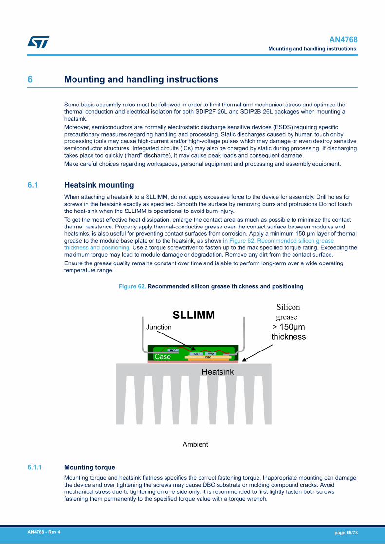
6 Mounting and handling instructions
Some basic assembly rules must be followed in order to limit thermal and mechanical stress and optimize thethermal conduction and electrical isolation for both SDIP2F-26L and SDIP2B-26L packages when mounting aheatsink.Moreover, semiconductors are normally electrostatic discharge sensitive devices (ESDS) requiring specificprecautionary measures regarding handling and processing. Static discharges caused by human touch or byprocessing tools may cause high-current and/or high-voltage pulses which may damage or even destroy sensitivesemiconductor structures. Integrated circuits (ICs) may also be charged by static during processing. If dischargingtakes place too quickly (“hard” discharge), it may cause peak loads and consequent damage.Make careful choices regarding workspaces, personal equipment and processing and assembly equipment.
6.1 Heatsink mountingWhen attaching a heatsink to a SLLIMM, do not apply excessive force to the device for assembly. Drill holes forscrews in the heatsink exactly as specified. Smooth the surface by removing burrs and protrusions Do not touchthe heat-sink when the SLLIMM is operational to avoid burn injury.To get the most effective heat dissipation, enlarge the contact area as much as possible to minimize the contactthermal resistance. Properly apply thermal-conductive grease over the contact surface between modules andheatsinks, is also useful for preventing contact surfaces from corrosion. Apply a minimum 150 μm layer of thermalgrease to the module base plate or to the heatsink, as shown in Figure 62. Recommended silicon greasethickness and positioning. Use a torque screwdriver to fasten up to the max specified torque rating. Exceeding themaximum torque may lead to module damage or degradation. Remove any dirt from the contact surface.Ensure the grease quality remains constant over time and is able to perform long-term over a wide operatingtemperature range.
Figure 62. Recommended silicon grease thickness and positioning
SLLIMM
Ambient
Heatsink
Case
Junction
DBCIGBT FWD
HVIC
Case
Silicongrease
> 150μmthickness
6.1.1 Mounting torqueMounting torque and heatsink flatness specifies the correct fastening torque. Inappropriate mounting can damagethe device and over tightening the screws may cause DBC substrate or molding compound cracks. Avoidmechanical stress due to tightening on one side only. It is recommended to first lightly fasten both screwsfastening them permanently to the specified torque value with a torque wrench.
AN4768Mounting and handling instructions
AN4768 - Rev 4 page 65/78
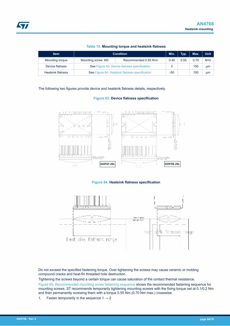
Table 15. Mounting torque and heatsink flatness
Item Condition Min. Typ. Max. Unit
Mounting torque Mounting screw: M3 Recommended 0.55 N•m 0.40 0.55 0.70 N•m
Device flatness See Figure 63. Device flatness specification 0 150 μm
Heatsink flatness See Figure 64. Heatsink flatness specification -50 100 μm
The following two figures provide device and heatsink flatness details, respectively.
Figure 63. Device flatness specification
SDIP2F-26L SDIP2B-26L
Figure 64. Heatsink flatness specification
Do not exceed the specified fastening torque. Over tightening the screws may cause ceramic or moldingcompound cracks and heat-fin threaded hole destruction.Tightening the screws beyond a certain torque can cause saturation of the contact thermal resistance.Figure 65. Recommended mounting screw fastening sequence shows the recommended fastening sequence formounting screws. ST recommends temporarily tightening mounting screws with the fixing torque set at 0.1/0.2 Nmand then permanently screwing them with a torque 0.55 Nm (0.70 Nm max.) crosswise.1. Fasten temporarily in the sequence 1 → 2
AN4768Heatsink mounting
AN4768 - Rev 4 page 66/78

2. Screw down permanently in the sequence 1 → 2When using electrical or pneumatic screwdrivers, ST suggests limiting the revolution to 200 rpm as the rapidimpact of the screw may damage the module plastic body.
Figure 65. Recommended mounting screw fastening sequence
Many other precautions regarding handling and contamination, ESD, storage, transportation and soldering shouldbe considered, and further details are available in technical note TN1220.
AN4768Heatsink mounting
AN4768 - Rev 4 page 67/78
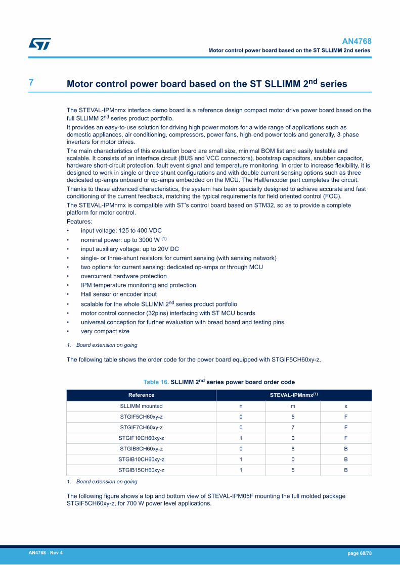
7 Motor control power board based on the ST SLLIMM 2nd series
The STEVAL-IPMnmx interface demo board is a reference design compact motor drive power board based on thefull SLLIMM 2nd series product portfolio.It provides an easy-to-use solution for driving high power motors for a wide range of applications such asdomestic appliances, air conditioning, compressors, power fans, high-end power tools and generally, 3-phaseinverters for motor drives.The main characteristics of this evaluation board are small size, minimal BOM list and easily testable andscalable. It consists of an interface circuit (BUS and VCC connectors), bootstrap capacitors, snubber capacitor,hardware short-circuit protection, fault event signal and temperature monitoring. In order to increase flexibility, it isdesigned to work in single or three shunt configurations and with double current sensing options such as threededicated op-amps onboard or op-amps embedded on the MCU. The Hall/encoder part completes the circuit.Thanks to these advanced characteristics, the system has been specially designed to achieve accurate and fastconditioning of the current feedback, matching the typical requirements for field oriented control (FOC).The STEVAL-IPMnmx is compatible with ST’s control board based on STM32, so as to provide a completeplatform for motor control.Features:• input voltage: 125 to 400 VDC• nominal power: up to 3000 W (1)
• input auxiliary voltage: up to 20V DC• single- or three-shunt resistors for current sensing (with sensing network)• two options for current sensing: dedicated op-amps or through MCU• overcurrent hardware protection• IPM temperature monitoring and protection• Hall sensor or encoder input• scalable for the whole SLLIMM 2nd series product portfolio• motor control connector (32pins) interfacing with ST MCU boards• universal conception for further evaluation with bread board and testing pins• very compact size
1. Board extension on going
The following table shows the order code for the power board equipped with STGIF5CH60xy-z.
Table 16. SLLIMM 2nd series power board order code
Reference STEVAL-IPMnmx(1)
SLLIMM mounted n m x
STGIF5CH60xy-z 0 5 F
STGIF7CH60xy-z 0 7 F
STGIF10CH60xy-z 1 0 F
STGIB8CH60xy-z 0 8 B
STGIB10CH60xy-z 1 0 B
STGIB15CH60xy-z 1 5 B
1. Board extension on going
The following figure shows a top and bottom view of STEVAL-IPM05F mounting the full molded packageSTGIF5CH60xy-z, for 700 W power level applications.
AN4768Motor control power board based on the ST SLLIMM 2nd series
AN4768 - Rev 4 page 68/78

Figure 66. Top and bottom view of STEVAL-IPM05F
AN4768Motor control power board based on the ST SLLIMM 2nd series
AN4768 - Rev 4 page 69/78

8 References
STGIF5CH60xy-z datasheetSTGIF7CH60xy-z datasheetSTGIF10CH60xy-z datasheetSTGIB8CH60xy-z datasheetSTGIB10CH60xy-z datasheetSTGIB15CH60xy-z datasheetSTGIB20M60xy-z datasheetSTGIB30M60xy-z datasheetSTEVAL-IPM05F evaluation boardSTEVAL-IPM07F evaluation boardSTEVAL-IPM10F evaluation boardSTEVAL-IPM08B evaluation boardSTEVAL-IPM10B evaluation boardSTEVAL-IPM15B evaluation boardAN3338 – “SLLIMM”AN4694 – “EMC design guides for motor control applications”TN1220 – “Mounting instruction for SLLIMM™ 2nd series”
AN4768References
AN4768 - Rev 4 page 70/78

Revision history
Table 17. Document revision history
Date Revision Changes
22-Oct-2015 1 First release.
30-Oct-2015 2
In Undervoltage lockout:
- Timing chart of undervoltage lockout function on low-side section and relevant stepsbelow figure.
In Motor control power board based on the ST SLLIMM 2nd series:
- changed text "...STGIF5CH60xy-z, for 500 W power level applications..." to"...STGIF5CH60xy-z, for 700 W power level applications..."
09-Jan-2017 3
Minor text and formatting changes throughout document.
Added text content between Figure 5: "Stray inductance components of output stage"and Table 6: "Control part of STGIF5CH60xy-z"
Added Section 1.5: "SCSOA"
In Section 2.3.5: "Short-circuit protection and smart shutdown function"
- added sentence: "If the short-circuit is present during restart..." and correspondingnote.
- updated Figure 18: "Smart shutdown equivalent circuitry"
Updated Figure 19: "Timing chart of smart shutdown function" and correspondingdescriptions for t1 to t7
Updated Figure 22: "Smart shutdown operation", Figure 25: "SD duration for OCevent", Figure 32: "Thermal sensor voltage vs temperature", Figure 35: "NTCresistance vs temperature", Figure 36: "NTC resistance vs temperature – zoom"
Added Figure 38: "VNTC vs temperature (pull up configuration)" and Figure 39:"VNTC vs temperature (pull down configuration)"
Updated Figure 47: "SDIP2F-26L and SDIP2B-26L – short leads and emitter forwardpackage" and Figure 48: "SDIP2F-26L and SDIP2B-26L – long leads package"
Updated Equation 29
In Section 5.1: "Typical circuit and recommendations"
- updated point 1
In Section 5.3: "General suggestions"
- updated point 8
Updated Table 16: "SLLIMM 2nd series power board order code"
AN4768
AN4768 - Rev 4 page 71/78
Date Revision Changes
17-May-2018 4
Updated Section "Introduction" (delete note a).
Updated curves in Section 1.5 SCSOAand Table 1. SLLIMM 1st and 2nd seriesdifferences.
Updated Section 1.2 Product line-up and nomenclature and Table 4. Synoptic table forDBC package option.
Updated Section 1.3 Internal circuit and Section 2.1 IGBTs section.
Updated Section 2.3.5 Short-circuit protection and smart shutdown function.
Updated Table 10. SD duration time per event and Section 2.3.9 Fault management.
Updated Section 2.3.10 Temperature monitoring and Figure 1.
Updated Figure 47. Thermal resistance comparison and Table 12. Rth(j-c) comparison.
Updated Table 13. SDIP2x-25/26L input and output pins
Updated Figure 2 and Table 2.
Updated Figure 58. Maximum IC(RMS) current vs. fsw simulated curves.
Updated Table 16. SLLIMM 2nd series power board order code.
Updated Section 8 References.
Minor text and formatting changes throughout document.
AN4768
AN4768 - Rev 4 page 72/78

Contents
1 Comparison of SLLIMM 1st and 2nd series. . . . . . . . . . . . . . . . . . . . . . . . . . . . . . . . . . . . . . . . . .2
1.1 Product synopsis . . . . . . . . . . . . . . . . . . . . . . . . . . . . . . . . . . . . . . . . . . . . . . . . . . . . . . . . . . . . . . . 2
1.2 Product line-up and nomenclature . . . . . . . . . . . . . . . . . . . . . . . . . . . . . . . . . . . . . . . . . . . . . . . . 4
1.3 Internal circuit . . . . . . . . . . . . . . . . . . . . . . . . . . . . . . . . . . . . . . . . . . . . . . . . . . . . . . . . . . . . . . . . . 6
1.4 Absolute maximum ratings. . . . . . . . . . . . . . . . . . . . . . . . . . . . . . . . . . . . . . . . . . . . . . . . . . . . . . . 8
1.5 SCSOA. . . . . . . . . . . . . . . . . . . . . . . . . . . . . . . . . . . . . . . . . . . . . . . . . . . . . . . . . . . . . . . . . . . . . . 12
2 Electrical characteristics and functions . . . . . . . . . . . . . . . . . . . . . . . . . . . . . . . . . . . . . . . . . . .17
2.1 IGBTs . . . . . . . . . . . . . . . . . . . . . . . . . . . . . . . . . . . . . . . . . . . . . . . . . . . . . . . . . . . . . . . . . . . . . . . 17
2.2 Freewheeling diodes. . . . . . . . . . . . . . . . . . . . . . . . . . . . . . . . . . . . . . . . . . . . . . . . . . . . . . . . . . . 17
2.3 IC gate drivers . . . . . . . . . . . . . . . . . . . . . . . . . . . . . . . . . . . . . . . . . . . . . . . . . . . . . . . . . . . . . . . . 17
2.3.1 Logic inputs. . . . . . . . . . . . . . . . . . . . . . . . . . . . . . . . . . . . . . . . . . . . . . . . . . . . . . . . . . . . 19
2.3.2 High voltage level shift . . . . . . . . . . . . . . . . . . . . . . . . . . . . . . . . . . . . . . . . . . . . . . . . . . . 20
2.3.3 Undervoltage lockout . . . . . . . . . . . . . . . . . . . . . . . . . . . . . . . . . . . . . . . . . . . . . . . . . . . . 20
2.3.4 Comparators for fault sensing . . . . . . . . . . . . . . . . . . . . . . . . . . . . . . . . . . . . . . . . . . . . . . 22
2.3.5 Short-circuit protection and smart shutdown function . . . . . . . . . . . . . . . . . . . . . . . . . . . . 22
2.3.6 Timing chart of short-circuit protection and smart shutdown function. . . . . . . . . . . . . . . . . 24
2.3.7 Current sensing shunt resistor selection . . . . . . . . . . . . . . . . . . . . . . . . . . . . . . . . . . . . . . 25
2.3.8 RC filter network selection. . . . . . . . . . . . . . . . . . . . . . . . . . . . . . . . . . . . . . . . . . . . . . . . . 27
2.3.9 Fault management . . . . . . . . . . . . . . . . . . . . . . . . . . . . . . . . . . . . . . . . . . . . . . . . . . . . . . 30
2.3.10 Temperature monitoring . . . . . . . . . . . . . . . . . . . . . . . . . . . . . . . . . . . . . . . . . . . . . . . . . . 36
2.3.11 Bootstrap circuit . . . . . . . . . . . . . . . . . . . . . . . . . . . . . . . . . . . . . . . . . . . . . . . . . . . . . . . . 42
2.3.12 Output safe clamp. . . . . . . . . . . . . . . . . . . . . . . . . . . . . . . . . . . . . . . . . . . . . . . . . . . . . . . 46
3 Package . . . . . . . . . . . . . . . . . . . . . . . . . . . . . . . . . . . . . . . . . . . . . . . . . . . . . . . . . . . . . . . . . . . . . . . . . .47
3.1 Full molded structure . . . . . . . . . . . . . . . . . . . . . . . . . . . . . . . . . . . . . . . . . . . . . . . . . . . . . . . . . . 47
3.2 DBC structure . . . . . . . . . . . . . . . . . . . . . . . . . . . . . . . . . . . . . . . . . . . . . . . . . . . . . . . . . . . . . . . . 47
3.3 Package structure . . . . . . . . . . . . . . . . . . . . . . . . . . . . . . . . . . . . . . . . . . . . . . . . . . . . . . . . . . . . . 49
3.4 Input and output pin descriptions . . . . . . . . . . . . . . . . . . . . . . . . . . . . . . . . . . . . . . . . . . . . . . . . 51
3.4.1 High-side bias voltage pins / high-side bias voltage reference . . . . . . . . . . . . . . . . . . . . . 52
3.4.2 Gate driver bias voltage . . . . . . . . . . . . . . . . . . . . . . . . . . . . . . . . . . . . . . . . . . . . . . . . . . 52
3.4.3 Gate driver supply ground. . . . . . . . . . . . . . . . . . . . . . . . . . . . . . . . . . . . . . . . . . . . . . . . . 52
AN4768Contents
AN4768 - Rev 4 page 73/78

3.4.4 Signal input . . . . . . . . . . . . . . . . . . . . . . . . . . . . . . . . . . . . . . . . . . . . . . . . . . . . . . . . . . . . 52
3.4.5 Internal comparator non-inverting . . . . . . . . . . . . . . . . . . . . . . . . . . . . . . . . . . . . . . . . . . . 53
3.4.6 Shutdown / open-drain . . . . . . . . . . . . . . . . . . . . . . . . . . . . . . . . . . . . . . . . . . . . . . . . . . . 53
3.4.7 Thermistor. . . . . . . . . . . . . . . . . . . . . . . . . . . . . . . . . . . . . . . . . . . . . . . . . . . . . . . . . . . . . 53
3.4.8 Thermal sensor . . . . . . . . . . . . . . . . . . . . . . . . . . . . . . . . . . . . . . . . . . . . . . . . . . . . . . . . . 53
3.4.9 Positive DC-link. . . . . . . . . . . . . . . . . . . . . . . . . . . . . . . . . . . . . . . . . . . . . . . . . . . . . . . . . 53
3.4.10 Negative DC-link . . . . . . . . . . . . . . . . . . . . . . . . . . . . . . . . . . . . . . . . . . . . . . . . . . . . . . . . 53
3.4.11 Inverter Power Output . . . . . . . . . . . . . . . . . . . . . . . . . . . . . . . . . . . . . . . . . . . . . . . . . . . . 54
4 Power loss and dissipation . . . . . . . . . . . . . . . . . . . . . . . . . . . . . . . . . . . . . . . . . . . . . . . . . . . . . . .55
4.1 Conduction power losses . . . . . . . . . . . . . . . . . . . . . . . . . . . . . . . . . . . . . . . . . . . . . . . . . . . . . . . 55
4.2 Switching power losses . . . . . . . . . . . . . . . . . . . . . . . . . . . . . . . . . . . . . . . . . . . . . . . . . . . . . . . . 57
4.3 Thermal impedance overview . . . . . . . . . . . . . . . . . . . . . . . . . . . . . . . . . . . . . . . . . . . . . . . . . . . 58
4.4 Power loss calculation example . . . . . . . . . . . . . . . . . . . . . . . . . . . . . . . . . . . . . . . . . . . . . . . . . 61
5 Design and mounting guidelines . . . . . . . . . . . . . . . . . . . . . . . . . . . . . . . . . . . . . . . . . . . . . . . . . .62
5.1 Typical circuit and recommendations . . . . . . . . . . . . . . . . . . . . . . . . . . . . . . . . . . . . . . . . . . . . . 62
5.2 Layout suggestions . . . . . . . . . . . . . . . . . . . . . . . . . . . . . . . . . . . . . . . . . . . . . . . . . . . . . . . . . . . . 63
5.3 General suggestions. . . . . . . . . . . . . . . . . . . . . . . . . . . . . . . . . . . . . . . . . . . . . . . . . . . . . . . . . . . 63
6 Mounting and handling instructions. . . . . . . . . . . . . . . . . . . . . . . . . . . . . . . . . . . . . . . . . . . . . . .65
6.1 Heatsink mounting . . . . . . . . . . . . . . . . . . . . . . . . . . . . . . . . . . . . . . . . . . . . . . . . . . . . . . . . . . . . 65
6.1.1 Mounting torque . . . . . . . . . . . . . . . . . . . . . . . . . . . . . . . . . . . . . . . . . . . . . . . . . . . . . . . . 65
7 Motor control power board based on the ST SLLIMM 2nd series . . . . . . . . . . . . . . . . . . .68
8 References . . . . . . . . . . . . . . . . . . . . . . . . . . . . . . . . . . . . . . . . . . . . . . . . . . . . . . . . . . . . . . . . . . . . . . .70
Revision history . . . . . . . . . . . . . . . . . . . . . . . . . . . . . . . . . . . . . . . . . . . . . . . . . . . . . . . . . . . . . . . . . . . . . . .71
AN4768Contents
AN4768 - Rev 4 page 74/78
List of tables
Table 1. SLLIMM 1st and 2nd series differences . . . . . . . . . . . . . . . . . . . . . . . . . . . . . . . . . . . . . . . . . . . . . . . . . . . . . 2Table 2. Product line-up . . . . . . . . . . . . . . . . . . . . . . . . . . . . . . . . . . . . . . . . . . . . . . . . . . . . . . . . . . . . . . . . . . . . . 4Table 3. Synoptic table for full molded package option . . . . . . . . . . . . . . . . . . . . . . . . . . . . . . . . . . . . . . . . . . . . . . . . 5Table 4. Synoptic table for DBC package option . . . . . . . . . . . . . . . . . . . . . . . . . . . . . . . . . . . . . . . . . . . . . . . . . . . . . 5Table 5. Inverter part of STGIF5CH60xy-z . . . . . . . . . . . . . . . . . . . . . . . . . . . . . . . . . . . . . . . . . . . . . . . . . . . . . . . . . 8Table 6. Control part of STGIF5CH60xy-z . . . . . . . . . . . . . . . . . . . . . . . . . . . . . . . . . . . . . . . . . . . . . . . . . . . . . . . . 10Table 7. Supply voltage and operation behavior . . . . . . . . . . . . . . . . . . . . . . . . . . . . . . . . . . . . . . . . . . . . . . . . . . . . 11Table 8. Total STGIF5CH60xy-z system . . . . . . . . . . . . . . . . . . . . . . . . . . . . . . . . . . . . . . . . . . . . . . . . . . . . . . . . . 11Table 9. Integrated pull-down resistor values . . . . . . . . . . . . . . . . . . . . . . . . . . . . . . . . . . . . . . . . . . . . . . . . . . . . . . 20Table 10. SD duration time per event . . . . . . . . . . . . . . . . . . . . . . . . . . . . . . . . . . . . . . . . . . . . . . . . . . . . . . . . . . . . 30Table 11. Fault event summary effect on IGBT and SD . . . . . . . . . . . . . . . . . . . . . . . . . . . . . . . . . . . . . . . . . . . . . . . . 30Table 12. Rth(j-c) comparison . . . . . . . . . . . . . . . . . . . . . . . . . . . . . . . . . . . . . . . . . . . . . . . . . . . . . . . . . . . . . . . . . . 48Table 13. SDIP2x-25/26L input and output pins . . . . . . . . . . . . . . . . . . . . . . . . . . . . . . . . . . . . . . . . . . . . . . . . . . . . . 51Table 14. RC Cauer thermal network elements by device . . . . . . . . . . . . . . . . . . . . . . . . . . . . . . . . . . . . . . . . . . . . . . 61Table 15. Mounting torque and heatsink flatness . . . . . . . . . . . . . . . . . . . . . . . . . . . . . . . . . . . . . . . . . . . . . . . . . . . . 66Table 16. SLLIMM 2nd series power board order code . . . . . . . . . . . . . . . . . . . . . . . . . . . . . . . . . . . . . . . . . . . . . . . . 68Table 17. Document revision history . . . . . . . . . . . . . . . . . . . . . . . . . . . . . . . . . . . . . . . . . . . . . . . . . . . . . . . . . . . . . 71
AN4768List of tables
AN4768 - Rev 4 page 75/78

List of figuresFigure 1. SLLIMM block diagram . . . . . . . . . . . . . . . . . . . . . . . . . . . . . . . . . . . . . . . . . . . . . . . . . . . . . . . . . . . . . . 4Figure 2. SLLIMM 2nd series nomenclature . . . . . . . . . . . . . . . . . . . . . . . . . . . . . . . . . . . . . . . . . . . . . . . . . . . . . . . 6Figure 3. Internal circuit for SDIP2F-26L and SDIP2B-26L (without NTC). . . . . . . . . . . . . . . . . . . . . . . . . . . . . . . . . . . 7Figure 4. Internal circuit for SDIP2F-26L and SDIP2B-26L (with NTC) . . . . . . . . . . . . . . . . . . . . . . . . . . . . . . . . . . . . . 8Figure 5. Stray inductance components of output stage. . . . . . . . . . . . . . . . . . . . . . . . . . . . . . . . . . . . . . . . . . . . . . 10Figure 6. TC measurement point. . . . . . . . . . . . . . . . . . . . . . . . . . . . . . . . . . . . . . . . . . . . . . . . . . . . . . . . . . . . . . 12Figure 7. SCSOA test circuit . . . . . . . . . . . . . . . . . . . . . . . . . . . . . . . . . . . . . . . . . . . . . . . . . . . . . . . . . . . . . . . . 13Figure 8. SCSOA main data. . . . . . . . . . . . . . . . . . . . . . . . . . . . . . . . . . . . . . . . . . . . . . . . . . . . . . . . . . . . . . . . . 14Figure 9. Typical STGIF5CH60yy SCSOA curve. . . . . . . . . . . . . . . . . . . . . . . . . . . . . . . . . . . . . . . . . . . . . . . . . . . 14Figure 10. Typical STGIF7CH60yy SCSOA curve. . . . . . . . . . . . . . . . . . . . . . . . . . . . . . . . . . . . . . . . . . . . . . . . . . . 15Figure 11. Typical STGIx10CH60yy SCSOA curve . . . . . . . . . . . . . . . . . . . . . . . . . . . . . . . . . . . . . . . . . . . . . . . . . . 15Figure 12. Typical STGIB8CH60yy SCSOA curve. . . . . . . . . . . . . . . . . . . . . . . . . . . . . . . . . . . . . . . . . . . . . . . . . . . 15Figure 13. Typical STGIB15CH60yy SCSOA curve. . . . . . . . . . . . . . . . . . . . . . . . . . . . . . . . . . . . . . . . . . . . . . . . . . 16Figure 14. Typical STGIB20M60yy SCSOA curve. . . . . . . . . . . . . . . . . . . . . . . . . . . . . . . . . . . . . . . . . . . . . . . . . . . 16Figure 15. Typical STGIB30M60yy SCSOA curve. . . . . . . . . . . . . . . . . . . . . . . . . . . . . . . . . . . . . . . . . . . . . . . . . . . 16Figure 16. TFS and Planar IGBT technology comparison . . . . . . . . . . . . . . . . . . . . . . . . . . . . . . . . . . . . . . . . . . . . . 17Figure 17. High-side gate driver block diagram. . . . . . . . . . . . . . . . . . . . . . . . . . . . . . . . . . . . . . . . . . . . . . . . . . . . . 18Figure 18. Low-side gate driver block diagram . . . . . . . . . . . . . . . . . . . . . . . . . . . . . . . . . . . . . . . . . . . . . . . . . . . . . 19Figure 19. Timing chart of undervoltage lockout function on low-side section . . . . . . . . . . . . . . . . . . . . . . . . . . . . . . . . 21Figure 20. Timing chart of undervoltage lockout function on high-side section . . . . . . . . . . . . . . . . . . . . . . . . . . . . . . . 22Figure 21. Smart shutdown equivalent circuitry . . . . . . . . . . . . . . . . . . . . . . . . . . . . . . . . . . . . . . . . . . . . . . . . . . . . 24Figure 22. Timing chart of smart shutdown function . . . . . . . . . . . . . . . . . . . . . . . . . . . . . . . . . . . . . . . . . . . . . . . . . 25Figure 23. Examples of SC protection circuits . . . . . . . . . . . . . . . . . . . . . . . . . . . . . . . . . . . . . . . . . . . . . . . . . . . . . 27Figure 24. Example of a short-circuit event . . . . . . . . . . . . . . . . . . . . . . . . . . . . . . . . . . . . . . . . . . . . . . . . . . . . . . . 28Figure 25. Smart shutdown operation . . . . . . . . . . . . . . . . . . . . . . . . . . . . . . . . . . . . . . . . . . . . . . . . . . . . . . . . . . . 29Figure 26. OC event . . . . . . . . . . . . . . . . . . . . . . . . . . . . . . . . . . . . . . . . . . . . . . . . . . . . . . . . . . . . . . . . . . . . . . . 31Figure 27. UVLO event . . . . . . . . . . . . . . . . . . . . . . . . . . . . . . . . . . . . . . . . . . . . . . . . . . . . . . . . . . . . . . . . . . . . . 31Figure 28. SD duration for OC event . . . . . . . . . . . . . . . . . . . . . . . . . . . . . . . . . . . . . . . . . . . . . . . . . . . . . . . . . . . . 32Figure 29. SD duration for short UVLO event (≤ 50 μs) . . . . . . . . . . . . . . . . . . . . . . . . . . . . . . . . . . . . . . . . . . . . . . . 32Figure 30. SD duration for long UVLO event (> 70 μs). . . . . . . . . . . . . . . . . . . . . . . . . . . . . . . . . . . . . . . . . . . . . . . . 33Figure 31. Short UVLO event after OC event . . . . . . . . . . . . . . . . . . . . . . . . . . . . . . . . . . . . . . . . . . . . . . . . . . . . . . 34Figure 32. Long UVLO event after OC event . . . . . . . . . . . . . . . . . . . . . . . . . . . . . . . . . . . . . . . . . . . . . . . . . . . . . . 35Figure 33. Comparator triggering in UVLO condition . . . . . . . . . . . . . . . . . . . . . . . . . . . . . . . . . . . . . . . . . . . . . . . . . 36Figure 34. Temperature detection points (top view) . . . . . . . . . . . . . . . . . . . . . . . . . . . . . . . . . . . . . . . . . . . . . . . . . . 37Figure 35. Thermal sensor voltage vs temperature . . . . . . . . . . . . . . . . . . . . . . . . . . . . . . . . . . . . . . . . . . . . . . . . . . 38Figure 36. Normal voltage controller (MCU) . . . . . . . . . . . . . . . . . . . . . . . . . . . . . . . . . . . . . . . . . . . . . . . . . . . . . . . 38Figure 37. Low voltage controller (MCU): optional clamping . . . . . . . . . . . . . . . . . . . . . . . . . . . . . . . . . . . . . . . . . . . . 39Figure 38. NTC resistance vs temperature. . . . . . . . . . . . . . . . . . . . . . . . . . . . . . . . . . . . . . . . . . . . . . . . . . . . . . . . 40Figure 39. NTC resistance vs temperature – zoom . . . . . . . . . . . . . . . . . . . . . . . . . . . . . . . . . . . . . . . . . . . . . . . . . . 40Figure 40. Sample overtemperature protection circuit . . . . . . . . . . . . . . . . . . . . . . . . . . . . . . . . . . . . . . . . . . . . . . . . 41Figure 41. VNTC vs temperature (pull up configuration) . . . . . . . . . . . . . . . . . . . . . . . . . . . . . . . . . . . . . . . . . . . . . . . 42Figure 42. VNTC vs temperature (pull down configuration) . . . . . . . . . . . . . . . . . . . . . . . . . . . . . . . . . . . . . . . . . . . . . 42Figure 43. Bootstrap circuit . . . . . . . . . . . . . . . . . . . . . . . . . . . . . . . . . . . . . . . . . . . . . . . . . . . . . . . . . . . . . . . . . . 43Figure 44. Bootstrap capacitor vs. switching frequency . . . . . . . . . . . . . . . . . . . . . . . . . . . . . . . . . . . . . . . . . . . . . . . 45Figure 45. Initial bootstrap charging time . . . . . . . . . . . . . . . . . . . . . . . . . . . . . . . . . . . . . . . . . . . . . . . . . . . . . . . . . 46Figure 46. DBC structure. . . . . . . . . . . . . . . . . . . . . . . . . . . . . . . . . . . . . . . . . . . . . . . . . . . . . . . . . . . . . . . . . . . . 47Figure 47. Thermal resistance comparison . . . . . . . . . . . . . . . . . . . . . . . . . . . . . . . . . . . . . . . . . . . . . . . . . . . . . . . 48Figure 48. SDIP2F-26L external and internal representation . . . . . . . . . . . . . . . . . . . . . . . . . . . . . . . . . . . . . . . . . . . 49Figure 49. SDIP2B-26L external and internal representation . . . . . . . . . . . . . . . . . . . . . . . . . . . . . . . . . . . . . . . . . . . 49Figure 50. SDIP2F-26L and SDIP2B-26L – short leads and emitter forward package . . . . . . . . . . . . . . . . . . . . . . . . . . 50Figure 51. SDIP2F-26L and SDIP2B-26L – long leads package . . . . . . . . . . . . . . . . . . . . . . . . . . . . . . . . . . . . . . . . . 51
AN4768List of figures
AN4768 - Rev 4 page 76/78

Figure 52. Typical IGBT power losses . . . . . . . . . . . . . . . . . . . . . . . . . . . . . . . . . . . . . . . . . . . . . . . . . . . . . . . . . . . 55Figure 53. IGBT and diode approximate output characteristics . . . . . . . . . . . . . . . . . . . . . . . . . . . . . . . . . . . . . . . . . . 56Figure 54. STGIF5CH60xy-x typical switching waveforms . . . . . . . . . . . . . . . . . . . . . . . . . . . . . . . . . . . . . . . . . . . . . 58Figure 55. Equivalent thermal circuit with heatsink single IGBT . . . . . . . . . . . . . . . . . . . . . . . . . . . . . . . . . . . . . . . . . 59Figure 56. Thermal impedance curves . . . . . . . . . . . . . . . . . . . . . . . . . . . . . . . . . . . . . . . . . . . . . . . . . . . . . . . . . . 60Figure 57. Thermal impedance RC Cauer thermal network . . . . . . . . . . . . . . . . . . . . . . . . . . . . . . . . . . . . . . . . . . . . 60Figure 58. Maximum IC(RMS) current vs. fsw simulated curves. . . . . . . . . . . . . . . . . . . . . . . . . . . . . . . . . . . . . . . . . . . 61Figure 59. Typical application circuit . . . . . . . . . . . . . . . . . . . . . . . . . . . . . . . . . . . . . . . . . . . . . . . . . . . . . . . . . . . . 62Figure 60. Recommended snubber capacitor position . . . . . . . . . . . . . . . . . . . . . . . . . . . . . . . . . . . . . . . . . . . . . . . . 64Figure 61. PCB layout general suggestions . . . . . . . . . . . . . . . . . . . . . . . . . . . . . . . . . . . . . . . . . . . . . . . . . . . . . . . 64Figure 62. Recommended silicon grease thickness and positioning . . . . . . . . . . . . . . . . . . . . . . . . . . . . . . . . . . . . . . 65Figure 63. Device flatness specification. . . . . . . . . . . . . . . . . . . . . . . . . . . . . . . . . . . . . . . . . . . . . . . . . . . . . . . . . . 66Figure 64. Heatsink flatness specification . . . . . . . . . . . . . . . . . . . . . . . . . . . . . . . . . . . . . . . . . . . . . . . . . . . . . . . . 66Figure 65. Recommended mounting screw fastening sequence . . . . . . . . . . . . . . . . . . . . . . . . . . . . . . . . . . . . . . . . . 67Figure 66. Top and bottom view of STEVAL-IPM05F. . . . . . . . . . . . . . . . . . . . . . . . . . . . . . . . . . . . . . . . . . . . . . . . . 69
AN4768List of figures
AN4768 - Rev 4 page 77/78

IMPORTANT NOTICE – PLEASE READ CAREFULLY
STMicroelectronics NV and its subsidiaries (“ST”) reserve the right to make changes, corrections, enhancements, modifications, and improvements to STproducts and/or to this document at any time without notice. Purchasers should obtain the latest relevant information on ST products before placing orders. STproducts are sold pursuant to ST’s terms and conditions of sale in place at the time of order acknowledgement.
Purchasers are solely responsible for the choice, selection, and use of ST products and ST assumes no liability for application assistance or the design ofPurchasers’ products.
No license, express or implied, to any intellectual property right is granted by ST herein.
Resale of ST products with provisions different from the information set forth herein shall void any warranty granted by ST for such product.
ST and the ST logo are trademarks of ST. All other product or service names are the property of their respective owners.
Information in this document supersedes and replaces information previously supplied in any prior versions of this document.
© 2018 STMicroelectronics – All rights reserved
AN4768
AN4768 - Rev 4 page 78/78