
AN2316 Configuration Options for the USB58xx and...
96
2016 Microchip Technology Inc. DS00002316A-page 1 INTRODUCTION The Microchip USB58xx/USB59xx are a family of highly customizable USB 3.1 Gen 1 hubs. These configuration options are modifiable through any of the following methods: • SMBus: SMBus configuration of the hub must be completed every time hub is powered-on or reset. • OTP Memory: The USB58xx/USB59xx have 8 kB of internal One-Time Programmable memory. Configuration settings made via OTP memory writes are permanent and may only be undone by a subsequent OTP write with the default configuration setting. • SPI ROM: An external SPI ROM loaded with an image of the hub’s base firmware may be used for configuration settings. The the external SPI ROM emulates the operation of the firmware executing from the hub’s internal ROM. Configuration settings added to the base firmware image executing from the SPI ROM emulate the opera- tion of the hub’s OTP memory, but have the advantage of being written and erased an unlimited number of times. • USB Command: All registers can be accessed via USB command while the hub is enumerated to a USB host. This document covers the following topics: Section 1.0, "Configuration Sequence and Priority" Section 2.0, "Configuration Register Map" Section 3.0, "Configuration via SMBus" Section 4.0, "Configuration via OTP" Section 5.0, "Configuration via SPI ROM" Section 6.0, "Configuration via USB Command" REFERENCES The following documents should be referenced when using this application note. See your Microchip representative for availability. • USB5807 Datasheet • USB5806 Datasheet • USB5816 Datasheet • USB5826 Datasheet • USB5906 Datasheet • USB5916 Datasheet • USB5926 Datasheet • System Management Bus Specification, Version 1.0, http://smbus.org/specs AN2316 Configuration Options for the USB58xx and USB59xx Author: Andrew Rogers Microchip Technology, Inc.
Transcript of AN2316 Configuration Options for the USB58xx and...

AN2316Configuration Options for the USB58xx and USB59xx
INTRODUCTION
The Microchip USB58xx/USB59xx are a family of highly customizable USB 3.1 Gen 1 hubs. These configuration options are modifiable through any of the following methods:
• SMBus: SMBus configuration of the hub must be completed every time hub is powered-on or reset.
• OTP Memory: The USB58xx/USB59xx have 8 kB of internal One-Time Programmable memory. Configuration settings made via OTP memory writes are permanent and may only be undone by a subsequent OTP write with the default configuration setting.
• SPI ROM: An external SPI ROM loaded with an image of the hub’s base firmware may be used for configuration settings. The the external SPI ROM emulates the operation of the firmware executing from the hub’s internal ROM. Configuration settings added to the base firmware image executing from the SPI ROM emulate the opera-tion of the hub’s OTP memory, but have the advantage of being written and erased an unlimited number of times.
• USB Command: All registers can be accessed via USB command while the hub is enumerated to a USB host.
This document covers the following topics:
Section 1.0, "Configuration Sequence and Priority"
Section 2.0, "Configuration Register Map"
Section 3.0, "Configuration via SMBus"
Section 4.0, "Configuration via OTP"
Section 5.0, "Configuration via SPI ROM"
Section 6.0, "Configuration via USB Command"
REFERENCES
The following documents should be referenced when using this application note. See your Microchip representative for availability.
• USB5807 Datasheet
• USB5806 Datasheet
• USB5816 Datasheet
• USB5826 Datasheet
• USB5906 Datasheet
• USB5916 Datasheet
• USB5926 Datasheet
• System Management Bus Specification, Version 1.0, http://smbus.org/specs
Author: Andrew RogersMicrochip Technology, Inc.
2016 Microchip Technology Inc. DS00002316A-page 1

AN2316
1.0 CONFIGURATION SEQUENCE AND PRIORITY
The USB58xx/USB59xx follow a specific sequence during initialization and configuration. It is important to consider this sequence when configuring the hub, especially if a combination of configuration options are used.
1.1 Configuration Straps
Upon power-on, the hub will check all pin straps. Generally, pin strapping is recommended only if other methods of con-figuration will not be used. If, for example, using a SPI ROM for firmware, or if the OTP is be programmed, it is recom-mended to perform all configuration using those methods to avoid any possible collisions.
1.2 SPI ROM Check
After checking Configuration Straps, the hub will check the presence of a SPI ROM with a valid signature. If a valid firm-ware file is detected, the hub will execute the firmware from the SPI ROM device.
Note that Internal OTP is ignored when executing from a SPI ROM device. Instead, the SPI ROM has a memory space allocated within the SPI memory which can be loaded with “pseudo-OTP” configuration data. An OTP file can be loaded into this space and will configure the hub in a manner which is equivalent to the Internal OTP.
1.3 SMBus Configuration during SOC_CFG stage
After SPI ROM is checked, the hub will check the SMBus pins for the presence of pull-up resistors to 3.3V. If pull-ups are detected on both the SDA and SCL lines, the hub will enter the SOC_CFG stage and wait indefinitely for configura-tion to occur.
During this stage, the internal register data can be modified from the default values.
1.4 Internal OTP
After SMBus configuration is completed and the special SMBus attach command is sent, the OTP memory is read and any registers configured by the internal OTP will be modified. This will overwrite any modifications done to these regis-ters during SOC_CFG. Only registers specifically configured in the OTP configuration data will be modified. All others will load with internal ROM defaults or with the changes made during SOC_CFG.
1.5 Runtime Configuration
After OTP memory is loaded, the hub will enter Runtime. Any register may be modified during this time via SMBus or through USB via bridging through the internal Hub Feature Controller device.
While any register may be modified during runtime, certain functional changes are forbidden during runtime. For exam-ple, USB ports cannot be disabled or enabled during runtime, as there is no mechanism within the USB specification to allow for changes to the number of ports while actively enumerated to a USB host.
DS00002316A-page 2 2016 Microchip Technology Inc.

AN2316
2.0 CONFIGURATION REGISTER MAP
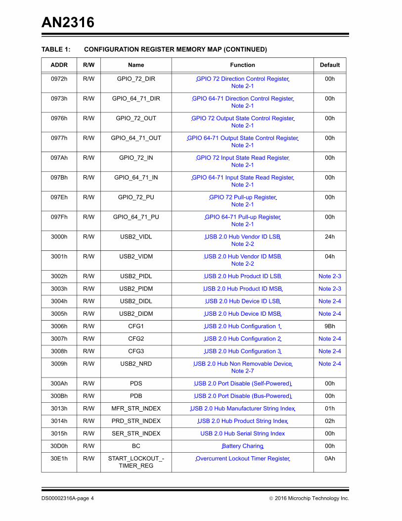
Below is a list of the configuration registers and their addresses. The default column displays the values that will be loaded into if no modification is made to the register during the configuration stage.
TABLE 1: CONFIGURATION REGISTER MEMORY MAP
ADDR R/W Name Function Default
082Dh R/W GPIO_16_23_PD GPIO 16-23 Pull-down RegisterNote 2-1
00h
082Eh R/W GPIO_8_12_PD GPIO 8-12 Pull-down RegisterNote 2-1
00h
082Fh R/W GPIO_1_7_PD GPIO 1-7 Pull-down RegisterNote 2-1
00h
0831h R/W GPIO_16_23_DIR GPIO 16-23 Direction Control RegisterNote 2-1
00h
0832h R/W GPIO_8_12_DIR GPIO 8-12 Direction Control RegisterNote 2-1
00h
0833h R/W GPIO_1_7_DIR GPIO 1-7 Direction Control RegisterNote 2-1
00h
0835h R/W GPIO_16_23_OUT GPIO 16-23 Output State Control RegisterNote 2-1
00h
0836h R/W GPIO_8_12_OUT GPIO 8-12 Output State Control RegisterNote 2-1
00h
0837h R/W GPIO_1_7_OUT GPIO 1-7 Output State Control RegisterNote 2-1
00h
0839h R/W GPIO_16_23_IN GPIO 16-23 Input State Read RegisterNote 2-1
00h
083Ah R/W GPIO_8_12_IN GPIO 8-12 Input State Read RegisterNote 2-1
00h
083Bh R/W GPIO_1_7_IN GPIO 1-7 Input State Read RegisterNote 2-1
00h
083Dh R/W GPIO_16_23_PU GPIO 16-23 Pull-up RegisterNote 2-1
00h
083Eh R/W GPIO_8_12_PU GPIO 8-12 Pull-up RegisterNote 2-1
00h
083Fh R/W GPIO_1_7_PU GPIO 1-7 Pull-up RegisterNote 2-1
00h
0900h R/W USB2_OCS_STAT USB 2.0 OCS Status Register 00h
0902h R/W USB3_OCS_STAT USB 3.0 OCS Status Register 00h
096Eh R/W GPIO_72_PD GPIO 72 Pull-down RegisterNote 2-1
00h
096Fh R/W GPIO_64_71_PD GPIO 64-71 Pull-down RegisterNote 2-1
00h
2016 Microchip Technology Inc. DS00002316A-page 3
AN2316
0972h R/W GPIO_72_DIR GPIO 72 Direction Control RegisterNote 2-1
00h
0973h R/W GPIO_64_71_DIR GPIO 64-71 Direction Control RegisterNote 2-1
00h
0976h R/W GPIO_72_OUT GPIO 72 Output State Control RegisterNote 2-1
00h
0977h R/W GPIO_64_71_OUT GPIO 64-71 Output State Control RegisterNote 2-1
00h
097Ah R/W GPIO_72_IN GPIO 72 Input State Read RegisterNote 2-1
00h
097Bh R/W GPIO_64_71_IN GPIO 64-71 Input State Read RegisterNote 2-1
00h
097Eh R/W GPIO_72_PU GPIO 72 Pull-up RegisterNote 2-1
00h
097Fh R/W GPIO_64_71_PU GPIO 64-71 Pull-up RegisterNote 2-1
00h
3000h R/W USB2_VIDL USB 2.0 Hub Vendor ID LSBNote 2-2
24h
3001h R/W USB2_VIDM USB 2.0 Hub Vendor ID MSBNote 2-2
04h
3002h R/W USB2_PIDL USB 2.0 Hub Product ID LSB Note 2-3
3003h R/W USB2_PIDM USB 2.0 Hub Product ID MSB Note 2-3
3004h R/W USB2_DIDL USB 2.0 Hub Device ID LSB Note 2-4
3005h R/W USB2_DIDM USB 2.0 Hub Device ID MSB Note 2-4
3006h R/W CFG1 USB 2.0 Hub Configuration 1 9Bh
3007h R/W CFG2 USB 2.0 Hub Configuration 2 Note 2-4
3008h R/W CFG3 USB 2.0 Hub Configuration 3 Note 2-4
3009h R/W USB2_NRD USB 2.0 Hub Non Removable DeviceNote 2-7
Note 2-4
300Ah R/W PDS USB 2.0 Port Disable (Self-Powered) 00h
300Bh R/W PDB USB 2.0 Port Disable (Bus-Powered) 00h
3013h R/W MFR_STR_INDEX USB 2.0 Hub Manufacturer String Index 01h
3014h R/W PRD_STR_INDEX USB 2.0 Hub Product String Index 02h
3015h R/W SER_STR_INDEX USB 2.0 Hub Serial String Index 00h
30D0h R/W BC Battery Charing 00h
30E1h R/W START_LOCKOUT_-TIMER_REG
Overcurrent Lockout Timer Register 0Ah
TABLE 1: CONFIGURATION REGISTER MEMORY MAP (CONTINUED)
ADDR R/W Name Function Default
DS00002316A-page 4 2016 Microchip Technology Inc.

AN2316
30EAh R/W OCS_MIN_WIDTH Overcurrent Minimum Pulse Width Register 05h
30EB R/W OCS_INACTIVE_-TIMER
Overcurrent Inactive Timer 14h
30FAh R/W PRT_SWAP USB 2.0 DP/DM Port Swap 00h
30FBh R/W USB2_PRT_REMAP_12
USB 2.0 Port 1 / Port 2 RemapNote 2-8
Note 2-4
30FCh R/W USB2_PRT_REMAP_34
USB 2.0 Port 3 / Port 4 RemapNote 2-8
Note 2-4
30FDh R/W USB2_PRT_REMAP_56
USB 2.0 Port 5 / Port 6 RemapNote 2-8
Note 2-4
30FEh R/W USB2_PRT_REMAP_7 USB 2.0 Port 7 RemapNote 2-8
Note 2-4
30FFh R/W HUB_CMD_STAT USB Hub Command / Status Register 00h
3100h R USB2_LINK_STATE1 USB Hub Command / Status Register FCh
3101h R USB2_LINK_STATE2 USB 2.0 Link State Ports 0 ~ 3 0Fh
3104h R/W USB2_HUB_CTL USB 2.0 Hub Control 00h
3108h R/W USB2_BCDUSB_MSB USB 2.0 Hub Version BCD MSB 02h
3109h R/W USB2_BCDUSB_LSB USB 2.0 Hub Version BCD LSB 10h
3150h R USB2_HUB_ADDR USB 2.0 Hub Address Register 00h
3151h R USB2_RE-MOTE_WAKE
USB 2.0 Hub Remote Wakeup Register 00h
318Ch R/W EMBED_TEST USB 2.0 Embedded Test modes Control 00h
318Dh R/W EMBED_TEST_PORT_SEL
USB 2.0 Embedded Test modes Port Select 00h
318Eh R/W CONNECT_CFG FlexConnect Configuration Register 00h
318Dh R USB20_HUB_STAT USB 2.0 Hub Status 00h
3195h R USB20_HUB_D-N_DEV_TYPE1
USB 2.0 Hub Downstream Port Device Speed Ports 1-4
00h
3196h R USB20_HUB_D-N_DEV_TYPE2
USB 2.0 Hub Downstream Port Device Speed Ports 5-7
00h
3197h R USB2_SUSP_IND USB2 SUSPEND Indicator 00h
3851h R USB30_HUB_STAT USB 3.1 Gen 1 Hub Status Register 00h
3857h R USB3_SUSP_IND USB3 SUSPEND Indicator 00h
3858h R/W USB3_PRT_REMAP_EN
USB3 Port Remap Enable Register Note 2-4
3860h R/W USB3_PRT_REMAP_12
USB3 Port Remap Ports 1 and 2Note 2-8
Note 2-4
TABLE 1: CONFIGURATION REGISTER MEMORY MAP (CONTINUED)
ADDR R/W Name Function Default
2016 Microchip Technology Inc. DS00002316A-page 5

AN2316
3861h R/W USB3_PRT_REMAP_34
USB3 Port Remap Ports 3 and 4Note 2-8
Note 2-4
3862h R/W USB3_PRT_REMAP_56
USB3 Port Remap Ports 5 and 6Note 2-8
Note 2-4
3863h R/W USB3_PRT_REMAP_7 USB3 Port Remap Port 7 Note 2-4
3870h R/W LINK_PWR_STATE1 USB 3.0 Link Low Power State 1 AAh
3874h R/W LINK_PWR_STATE2 USB 3.0 Link Low Power State 2 02h
3C00h R/W USB3_PRT_CFG_-SEL1
USB 3.1 Gen 1 Port 1 Configuration SelectNote 2-8
83h
3C04h R/W USB3_PRT_CFG_-SEL2
USB 3.1 Gen 1 Port 2 Configuration SelectNote 2-8
Note 2-4
3C08h R/W USB3_PRT_CFG_-SEL3
USB 3.1 Gen 1 Port 3 Configuration SelectNote 2-8
83h
3C0Ch R/W USB3_PRT_CFG_-SEL4
USB 3.1 Gen 1 Port 4 Configuration SelectNote 2-8
Note 2-4
3C10h R/W USB3_PRT_CFG_-SEL5
USB 3.1 Gen 1 Port 5 Configuration SelectNote 2-8
83h
3C14h R/W USB3_PRT_CFG_-SEL6
USB 3.1 Gen 1 Port 6 Configuration SelectNote 2-8
83h
3C18h R/W USB3_PRT_CFG_-SEL7
USB 3.1 Gen 1 Port 7 Configuration SelectNote 2-8
Note 2-4
3C20h R/W OCS_SEL1 Port 1 Overcurrent Sense Source Select 01h
3C24h R/W OCS_SEL2 Port 2 Overcurrent Sense Source Select 01h
3C28h R/W OCS_SEL3 Port 3 Overcurrent Sense Source Select 01h
3C2Ch R/W OCS_SEL4 Port 4 Overcurrent Sense Source Select 01h
3C30 R/W OCS_SEL5 Port 5 Overcurrent Sense Source Select 01h
3C34 R/W OCS_SEL6 Port 6 Overcurrent Sense Source Select 01h
3C38 R/W OCS_SEL7 Port 7 Overcurrent Sense Source Select 01h
411Ah R/W FLEX_CFG1 FlexConnect Configuration 1 00h
411Bh R/W FLEX_CFG2 FlexConnect Configuration 2 00h
4130h R/W HFC_EN Hub Feature Controller Enable 00h
413Ch R/W DETACH_TIM-ER_A_LSB
Billboard Detach Timer A LSB D0h
413Dh R/W DETACH_TIM-ER_A_MSB
Billboard Detach Timer A MSB 07h
413Eh R/W DETACH_TIM-ER_B_LSB
Billboard Detach Timer B LSB D0h
TABLE 1: CONFIGURATION REGISTER MEMORY MAP (CONTINUED)
ADDR R/W Name Function Default
DS00002316A-page 6 2016 Microchip Technology Inc.

AN2316
413Fh R/W DETACH_TIM-ER_B_MSB
Billboard Detach Timer B MSB 07h
416Dh R/W PORT_SPLIT_A_SE-LECT
Port Split PRTPWRx_USB3_SPLIT Control Select 1
00h
416Eh R/W PORT_SPLIT_B_SE-LECT
Port Split PRTPWRx_USB3_SPLIT Control Select 2
00h
4171h R/W USB_PORT_SPLIT_-TIMEOUT
USB3 Port Split Link Timeout 05h
4176h R/W USB3_PORT_SPLIT_-TOGGLE_TIME
USB3 Port Split Toggle Time 05h
4178h R/W BC_CFG_P1 Battery Charging Port 1 Configuration 00h
4179h R/W BC_CFG_P2 Battery Charging Port 2 Configuration 00h
417Ah R/W BC_CFG_P3 Battery Charging Port 3 Configuration 00h
417Bh R/W BC_CFG_P4 Battery Charging Port 4 Configuration 00h
417Ch R/W BC_CFG_P5 Battery Charging Port 5 Configuration 00h
417Dh R/W BC_CFG_P6 Battery Charging Port 6 Configuration 00h
417Eh R/W BC_CFG_P7 Battery Charging Port 7 Configuration 00h
4177h R/W FLEX_CONTROL_REG FlexConnect Control Register 04h
4448h R/W USB3_VIDL USB 3.0 Hub Vendor ID LSBNote 2-2
24h
4449h R/W USB3_VIDM USB 3.0 Hub Vendor ID MSBNote 2-2
04h
444Ah R/W USB3_PIDL USB 3.0 Hub Product ID LSB Note 2-9
444Bh R/W USB3_PIDM USB 3.0 Hub Product ID MSB Note 2-9
444Ch R/W USB3_DIDL USB 3.0 Hub Device ID LSB Note 2-4
444Dh R/W USB3_DIDM USB 3.0 Hub Device ID MSB Note 2-4
44A2h R/W USB3_NBR_PRTS USB 3.0 Number of PortsNote 2-8
Note 2-4
44A3h R/W USB3_COMPOUND USB 3.0 Hub Compound DeviceNote 2-7
Note 2-4
44AAh R/W USB3_NRD USB 3.0 Hub Non Removable DeviceNote 2-7
02h
60CAh R/W HS_UP_BOOST USB 2.0 Upstream PHYBoost Register 00h
60CCh R/W HS_UP_SENSE USB 2.0 Upstream Varisense Register 00h
64CAh R/W HS_P1_BOOST USB 2.0 Downstream Port 1 PHYBoost Register 00h
64CCh R/W HS_P1_SENSE USB 2.0 Downstream Port 1 Varisense Register 00h
TABLE 1: CONFIGURATION REGISTER MEMORY MAP (CONTINUED)
ADDR R/W Name Function Default
2016 Microchip Technology Inc. DS00002316A-page 7

AN2316
Note 2-1 See Microchip AN1997 USB to GPIO Bridging with Microchip USB 3.1 Gen 1 Hubs for details on how to configure the hub for GPIO control.
Note 2-2 The Vendor ID LSB and MSB must be assigned the same value for both the USB 2.0 Hub and USB 3.0 Hub registers. Failure to correctly modify these registers may result in unpredictable behavior.
Note 2-3 The default value of the VID registers are dependent on part number. USB5806 = 0x2806, USB5807 = 0x2807, USB5816 = 0x2816, USB5826 = 0x2826, USB5906 = 0x2906, USB5916 = 0x2916, USB5926 = 0x2926.
Note 2-4 The default value of this register will vary dependent on the device firmware and silicon revision.
Note 2-5 The default value of this register is dependent on part number. USB5807 = 0x20, USB5806/USB5816/USB5826/USB5906/USB5916/USB5917 = 0x28.
Note 2-6 The default value of this register is dependent on part number. USB5807 = 0x00, USB5806/USB5816/USB5826/USB5906/USB5916/USB5917 = 0x20.
Note 2-7 The Non-Removable Device settings must be assigned the same value for both the USB 2.0 Hub and USB 3.0 Hub registers. Failure to correctly modify these registers may result in unpredictable behavior.
Note 2-8 The Port Disable/Remap settings must be assigned the same value for both the USB 2.0 Hub and USB 3.0 Hub registers. Failure to correctly modify these registers may result in unpredictable behavior.
Note 2-9 The default value of the PID registers are dependent on part number. USB5806 = 0x5806, USB5807 = 0x5807, USB5816 = 0x5816, USB5826 = 0x5826, USB5906 = 0x5906, USB5916 = 0x5916, USB5926 = 0x5926.
68CAh R/W HS_P2_BOOST USB 2.0 Downstream Port2 PHYBoost Register 00h
68CCh R/W HS_P2_SENSE USB 2.0 Downstream Port 2 Varisense Register 00h
6CCAh R/W HS_P3_BOOST USB 2.0 Downstream Port 3 PHYBoost Register 00h
6CCCh R/W HS_P3_SENSE USB 2.0 Downstream Port 3 Varisense Register 00h
70CAh R/W HS_P4_BOOST USB 2.0 Downstream Port 4 PHYBoost Register 00h
70CCh R/W HS_P4_SENSE USB 2.0 Downstream Port 4 Varisense Register 00h
74CAh R/W HS_P5_BOOST USB 2.0 Downstream Port 5 PHYBoost Register 00h
74CCh R/W HS_P5_SENSE USB 2.0 Downstream Port 5 Varisense Register 00h
78CAh R/W HS_P6_BOOST USB 2.0 Downstream Port 6 PHYBoost Register 00h
78CCh R/W HS_P6_SENSE USB 2.0 Downstream Port 6 Varisense Register 00h
7CCAh R/W HS_P7_BOOST USB 2.0 Downstream Port 7 PHYBoost Register 00h
7CCCh R/W HS_P7_SENSE USB 2.0 Downstream Port 7 Varisense Register 00h
TABLE 1: CONFIGURATION REGISTER MEMORY MAP (CONTINUED)
ADDR R/W Name Function Default
DS00002316A-page 8 2016 Microchip Technology Inc.

AN2316
2.1 Register Definitions
TABLE 2: GPIO 16-23 PULL-DOWN REGISTER
GPIO_16_23_PD(082Dh)
GPIO 16-23 Pull-down Register
BIT Name R/W Description
7 GPIO_23_PD R/W Set bit to enable GPIO23 Pull-down resistor.
6 GPIO_22_PD R/W Set bit to enable GPIO22 Pull-down resistor.
5 GPIO_21_PD R/W Set bit to enable GPIO21 Pull-down resistor.
4 GPIO_20_PD R/W Set bit to enable GPIO20 Pull-down resistor.
3 GPIO_19_PD R/W Set bit to enable GPIO19 Pull-down resistor.
2 GPIO_18_PD R/W Set bit to enable GPIO18 Pull-down resistor.
1 GPIO_17_PD R/W Set bit to enable GPIO17 Pull-down resistor.
0 GPIO_16_PD R/W Set bit to enable GPIO16 Pull-down resistor.
TABLE 3: GPIO 8-12 PULL-DOWN REGISTER
GPIO_8_12_PD(082Eh)
GPIO 8-12 Pull-down Register
BIT Name R/W Description
7:5 Reserved R Reserved
4 GPIO_12_PD R/W —
3 Reserved R Reserved
2 GPIO_10_PD R/W Set bit to enable GPIO10 Pull-down resistor.
1 GPIO_9_PD R/W Set bit to enable GPIO9 Pull-down resistor.
0 GPIO_8_PD R/W Set bit to enable GPIO8 Pull-down resistor.
TABLE 4: GPIO 1-7 PULL-DOWN REGISTER
GPIO_1_7_PD(082Fh)
GPIO 1-7 Pull-down Register
BIT Name R/W Description
7 GPIO_7_PD R/W Set bit to enable GPIO7 Pull-down resistor.
6 GPIO_6_PD R/W Set bit to enable GPIO6 Pull-down resistor.
5 GPIO_5_PD R/W Set bit to enable GPIO5 Pull-down resistor.
4 GPIO_4_PD R/W Set bit to enable GPIO4 Pull-down resistor.
2016 Microchip Technology Inc. DS00002316A-page 9

AN2316
3 GPIO_3_PD R/W Set bit to enable GPIO3 Pull-down resistor.
2 GPIO_2_PD R/W Set bit to enable GPIO2 Pull-down resistor.
1 GPIO_1_PD R/W Set bit to enable GPIO1 Pull-down resistor.
0 Reserved R Reserved
TABLE 5: GPIO 16-23 DIRECTION CONTROL REGISTER
GPIO_16_23_DIR(0831h)
GPIO 16-23 Direction Control Register
BIT Name R/W Description
7 GPIO_23_DIR R/W Set bit to configure GPIO16 as an output. Clear to set as Input.
6 GPIO_23_DIR R/W Set bit to configure GPIO16 as an output. Clear to set as Input.
5 GPIO_23_DIR R/W Set bit to configure GPIO16 as an output. Clear to set as Input.
4 GPIO_16_DIR R/W Set bit to configure GPIO16 as an output. Clear to set as Input.
3 GPIO_16_DIR R/W Set bit to configure GPIO16 as an output. Clear to set as Input.
2 GPIO_16_DIR R/W Set bit to configure GPIO16 as an output. Clear to set as Input.
1 GPIO_16_DIR R/W Set bit to configure GPIO16 as an output. Clear to set as Input.
0 GPIO_16_DIR R/W Set bit to configure GPIO16 as an output. Clear to set as Input.
TABLE 6: GPIO 8-12 DIRECTION CONTROL REGISTER
GPIO_8_12_DIR(0832h)
GPIO 8-12 Direction Control Register
BIT Name R/W Description
7:5 Reserved R Reserved
4 GPIO_12_DIR R/W Set bit to configure GPIO12 as an output. Clear to set as Input.
3 Reserved R Reserved
2 GPIO_10_DIR R/W Set bit to configure GPIO10 as an output. Clear to set as Input.
1 GPIO_9_DIR R/W Set bit to configure GPIO9 as an output. Clear to set as Input.
0 GPIO_8_DIR R/W Set bit to configure GPIO8 as an output. Clear to set as Input.
TABLE 4: GPIO 1-7 PULL-DOWN REGISTER (CONTINUED)
GPIO_1_7_PD(082Fh)
GPIO 1-7 Pull-down Register
BIT Name R/W Description
DS00002316A-page 10 2016 Microchip Technology Inc.

AN2316
TABLE 7: GPIO 1-7 DIRECTION CONTROL REGISTER
GPIO_1_7_DIR(0833h)
GPIO 1-7 Direction Control Register
BIT Name R/W Description
7 GPIO_7_DIR R/W Set bit to configure GPIO7 as an output. Clear to set as Input.
6 GPIO_6_DIR R/W Set bit to configure GPIO6 as an output. Clear to set as Input.
5 GPIO_5_DIR R/W Set bit to configure GPIO5 as an output. Clear to set as Input.
4 GPIO_4_DIR R/W Set bit to configure GPIO4 as an output. Clear to set as Input.
3 GPIO_3_DIR R/W Set bit to configure GPIO3 as an output. Clear to set as Input.
2 GPIO_2_DIR R/W Set bit to configure GPIO2 as an output. Clear to set as Input.
1 GPIO_1_DIR R/W Set bit to configure GPIO1 as an output. Clear to set as Input.
0 Reserved R Reserved
TABLE 8: GPIO 16-23 OUTPUT STATE CONTROL REGISTER
GPIO_16_23_OUT(0835h)
GPIO 16-23 Output State Control Register
BIT Name R/W Description
7 GPIO_23_OUT R/W Sets the state of GPIO23 when configured as an output
6 GPIO_22_OUT R/W Sets the state of GPIO22 when configured as an output
5 GPIO_21_OUT R/W Sets the state of GPIO21 when configured as an output
4 GPIO_20_OUT R/W Sets the state of GPIO20 when configured as an output
3 GPIO_19_OUT R/W Sets the state of GPIO19 when configured as an output
2 GPIO_18_OUT R/W Sets the state of GPIO18 when configured as an output
1 GPIO_17_OUT R/W Sets the state of GPIO17 when configured as an output
0 GPIO_16_OUT R/W Sets the state of GPIO16 when configured as an output
TABLE 9: GPIO 8-12 OUTPUT STATE CONTROL REGISTER
GPIO_8_12_OUT(0836h)
GPIO 8-12 Output State Control Register
BIT Name R/W Description
7:5 Reserved R Reserved
4 GPIO_12_OUT R/W Sets the state of GPIO12 when configured as an output
2016 Microchip Technology Inc. DS00002316A-page 11

AN2316
3 Reserved R Reserved
2 GPIO_10_OUT R/W Sets the state of GPIO10 when configured as an output
1 GPIO_9_OUT R/W Sets the state of GPIO9 when configured as an output
0 GPIO_8_OUT R/W Sets the state of GPIO8 when configured as an output
TABLE 10: GPIO 1-7 OUTPUT STATE CONTROL REGISTER
GPIO_1_7_OUT(0837h)
GPIO 1-7 Output State Control Register
BIT Name R/W Description
7 GPIO_7_OUT R/W Sets the state of GPIO7 when configured as an output
6 GPIO_6_OUT R/W Sets the state of GPIO6 when configured as an output
5 GPIO_5_OUT R/W Sets the state of GPIO5 when configured as an output
4 GPIO_4_OUT R/W Sets the state of GPIO4 when configured as an output
3 GPIO_3_OUT R/W Sets the state of GPIO3 when configured as an output
2 GPIO_2_OUT R/W Sets the state of GPIO2 when configured as an output
1 GPIO_1_OUT R/W Sets the state of GPIO1 when configured as an output
0 Reserved R Reserved
TABLE 11: GPIO 16-23 INPUT STATE READ REGISTER
GPIO_16_23_IN(0839h)
GPIO 16-23 Input State Read Register
BIT Name R/W Description
7 GPIO_23_IN R Reads back the state of GPIO23 when configured as an input.
6 GPIO_22_IN R Reads back the state of GPIO22 when configured as an input.
5 GPIO_21_IN R Reads back the state of GPIO21 when configured as an input.
4 GPIO_20_IN R Reads back the state of GPIO20 when configured as an input.
3 GPIO_19_IN R Reads back the state of GPIO19 when configured as an input.
2 GPIO_18_IN R Reads back the state of GPIO18 when configured as an input.
1 GPIO_17_IN R Reads back the state of GPIO17 when configured as an input.
TABLE 9: GPIO 8-12 OUTPUT STATE CONTROL REGISTER (CONTINUED)
GPIO_8_12_OUT(0836h)
GPIO 8-12 Output State Control Register
BIT Name R/W Description
DS00002316A-page 12 2016 Microchip Technology Inc.

AN2316
0 GPIO_16_IN R Reads back the state of GPIO16 when configured as an input.
TABLE 12: GPIO 8-12 INPUT STATE READ REGISTER
GPIO_8_12_IN(083Ah)
GPIO 8-12 Input State Read Register
BIT Name R/W Description
7:5 Reserved R Reserved
4 GPIO_12_IN R Reads back the state of GPIO12 when configured as an input.
3 Reserved R Reserved
2 GPIO_10_IN R Reads back the state of GPIO10 when configured as an input.
1 GPIO_9_IN R Reads back the state of GPIO9 when configured as an input.
0 GPIO_8_IN R Reads back the state of GPIO8 when configured as an input.
TABLE 13: GPIO 1-7 INPUT STATE READ REGISTER
GPIO_1_7_IN(083Bh)
GPIO 1-7 Input State Read Register
BIT Name R/W Description
7 GPIO_7_IN R/W Reads back the state of GPIO7 when configured as an input.
6 GPIO_6_IN R/W Reads back the state of GPIO6 when configured as an input.
5 GPIO_5_IN R/W Reads back the state of GPIO5 when configured as an input.
4 GPIO_4_IN R/W Reads back the state of GPIO4 when configured as an input.
3 GPIO_3_IN R Reads back the state of GPIO3 when configured as an input.
2 GPIO_2_IN R Reads back the state of GPIO2 when configured as an input.
1 GPIO_1_IN R Reads back the state of GPIO1 when configured as an input.
0 Reserved R Reserved
TABLE 11: GPIO 16-23 INPUT STATE READ REGISTER (CONTINUED)
GPIO_16_23_IN(0839h)
GPIO 16-23 Input State Read Register
BIT Name R/W Description
2016 Microchip Technology Inc. DS00002316A-page 13

AN2316
TABLE 14: GPIO 8-12 PULL-UP REGISTER
GPIO_16_23_PU(083Dh)
GPIO 16-23 Pull-up Register
BIT Name R/W Description
7 GPIO_23_PU R/W Set bit to enable GPIO23 Pull-up resistor.
6 GPIO_22_PU R/W Set bit to enable GPIO22 Pull-up resistor.
5 GPIO_21_PU R/W Set bit to enable GPIO21 Pull-up resistor.
4 GPIO_20_PU R/W Set bit to enable GPIO20 Pull-up resistor.
3 GPIO_19_PU R/W Set bit to enable GPIO19 Pull-up resistor.
2 GPIO_18_PU R/W Set bit to enable GPIO18 Pull-up resistor.
1 GPIO_17_PU R/W Set bit to enable GPIO17 Pull-up resistor.
0 GPIO_16_PU R/W Set bit to enable GPIO16 Pull-up resistor.
TABLE 15: GPIO 16-23 PULL-UP REGISTER
GPIO_8_12_PU(083Eh)
GPIO 8-12 Pull-up Register
BIT Name R/W Description
7:5 Reserved R Reserved
4 GPIO_12_PU R/W Set bit to enable GPIO12 Pull-up resistor.
3 Reserved R Reserved
2 GPIO_10_PU R/W Set bit to enable GPIO10 Pull-up resistor.
1 GPIO_9_PU R/W Set bit to enable GPIO9 Pull-up resistor.
0 GPIO_8_PU R/W Set bit to enable GPIO8 Pull-up resistor.
TABLE 16: GPIO 1-7 PULL-UP REGISTER
GPIO_1_7_PU(083Fh)
GPIO 1-7 Pull-up Register
BIT Name R/W Description
7 GPIO_7_PU R/W Set bit to enable GPIO7 Pull-up resistor.
6 GPIO_6_PU R/W Set bit to enable GPIO6 Pull-up resistor.
5 GPIO_5_PU R/W Set bit to enable GPIO5 Pull-up resistor.
4 GPIO_4_PU R/W Set bit to enable GPIO4 Pull-up resistor.
DS00002316A-page 14 2016 Microchip Technology Inc.

AN2316
3 GPIO_3_PU R/W Set bit to enable GPIO3 Pull-up resistor.
2 GPIO_2_PU R/W Set bit to enable GPIO2 Pull-up resistor.
1 GPIO_1_PU R/W Set bit to enable GPIO1 Pull-up resistor.
0 Reserved R Reserved
TABLE 17: GPIO 72 PULL-DOWN REGISTER
GPIO_72_PD(096Eh)
GPIO 72 Pull-down Register
BIT Name R/W Description
7:1 Reserved R Reserved
0 GPIO_72_PD R/W Set bit to enable GPIO72 Pull-down resistor.
TABLE 18: GPIO 64-71 PULL-DOWN REGISTER
GPIO_64_71_PD(096Fh)
GPIO 64-71 Pull-down Register
BIT Name R/W Description
7 GPIO_71_PD R/W Set bit to enable GPIO71 Pull-down resistor.
6 GPIO_70_PD R/W Set bit to enable GPIO70 Pull-down resistor.
5 GPIO_69_PD R/W Set bit to enable GPIO69 Pull-down resistor.
4 GPIO_68_PD R/W Set bit to enable GPIO68 Pull-down resistor.
3 GPIO_67_PD R/W Set bit to enable GPIO67 Pull-down resistor.
2 GPIO_66_PD R/W Set bit to enable GPIO66 Pull-down resistor.
1 GPIO_65_PD R/W Set bit to enable GPIO65 Pull-down resistor.
0 GPIO_64_PD R/W Set bit to enable GPIO64 Pull-down resistor.
TABLE 16: GPIO 1-7 PULL-UP REGISTER (CONTINUED)
GPIO_1_7_PU(083Fh)
GPIO 1-7 Pull-up Register
BIT Name R/W Description
2016 Microchip Technology Inc. DS00002316A-page 15

AN2316
TABLE 19: GPIO 72 DIRECTION CONTROL REGISTER
GPIO_72_DIR(0972h)
GPIO 72 Direction Control Register
BIT Name R/W Description
7:1 Reserved R Reserved
0 GPIO_72_DIR R/W Set bit to configure GPIO72 as an output. Clear to set as Input.
TABLE 20: GPIO 64-71 DIRECTION CONTROL REGISTER
GPIO_64_71_DIR(0973h)
GPIO 64-71 Direction Control Register
BIT Name R/W Description
7 GPIO_71_DIR R/W Set bit to configure GPIO71 as an output. Clear to set as Input.
6 GPIO_70_DIR R/W Set bit to configure GPIO70 as an output. Clear to set as Input.
5 GPIO_69_DIR R/W Set bit to configure GPIO69 as an output. Clear to set as Input.
4 GPIO_68_DIR R/W Set bit to configure GPIO68 as an output. Clear to set as Input.
3 GPIO_67_DIR R/W Set bit to configure GPIO67 as an output. Clear to set as Input.
2 GPIO_66_DIR R/W Set bit to configure GPIO66 as an output. Clear to set as Input.
1 GPIO_65_DIR R/W Set bit to configure GPIO65 as an output. Clear to set as Input.
0 GPIO_64_DIR R/W Set bit to configure GPIO64 as an output. Clear to set as Input.
TABLE 21: GPIO 72 OUTPUT STATE CONTROL REGISTER
GPIO_72_OUT(0976h)
GPIO 72 Output State Control Register
BIT Name R/W Description
7:1 Reserved R Reserved
0 GPIO_72_OUT R/W Sets the state of GPIO72 when configured as an output
DS00002316A-page 16 2016 Microchip Technology Inc.

AN2316
TABLE 22: GPIO 64-71 OUTPUT STATE CONTROL REGISTER
GPIO_64_71_OUT(0977h)
GPIO 64-71 Output State Control Register
BIT Name R/W Description
7 GPIO_71_OUT R/W Sets the state of GPIO71 when configured as an output
6 GPIO_70_OUT R/W Sets the state of GPIO70 when configured as an output
5 GPIO_69_OUT R/W Sets the state of GPIO69 when configured as an output
4 GPIO_68_OUT R/W Sets the state of GPIO68 when configured as an output
3 GPIO_67_OUT R/W Sets the state of GPIO67 when configured as an output
2 GPIO_66_OUT R/W Sets the state of GPIO66 when configured as an output
1 GPIO_65_OUT R/W Sets the state of GPIO65 when configured as an output
0 GPIO_64_OUT R/W Sets the state of GPIO64 when configured as an output
TABLE 23: GPIO 72 INPUT STATE READ REGISTER
GPIO_72_IN(097Ah)
GPIO 72 Input State Read Register
BIT Name R/W Description
7:1 Reserved R Reserved
0 GPIO_72_IN R Reads back the state of GPIO72 when configured as an input.
TABLE 24: GPIO 64-71 INPUT STATE READ REGISTER
GPIO_64_71_IN(097Bh)
GPIO 64-71 Input State Read Register
BIT Name R/W Description
7 GPIO_71_IN R Reads back the state of GPIO71 when configured as an input.
6 GPIO_70_IN R Reads back the state of GPIO70 when configured as an input.
5 GPIO_69_IN R Reads back the state of GPIO69 when configured as an input.
4 GPIO_68_IN R Reads back the state of GPIO68 when configured as an input.
3 GPIO_67_IN R Reads back the state of GPIO67 when configured as an input.
2 GPIO_66_IN R Reads back the state of GPIO66 when configured as an input.
1 GPIO_65_IN R Reads back the state of GPIO65 when configured as an input.
0 GPIO_64_IN R Reads back the state of GPIO64 when configured as an input.
2016 Microchip Technology Inc. DS00002316A-page 17

AN2316
TABLE 25: GPIO 72 PULL-UP REGISTER
GPIO_72_PU(097Fh)
GPIO 72 Pull-up Register
BIT Name R/W Description
7:1 Reserved R Reserved
0 GPIO_72_PU R/W Set bit to enable GPIO72 Pull-up resistor.
TABLE 26: GPIO 64-71 PULL-UP REGISTER
GPIO_64_71_PU(097Fh)
GPIO 64-71 Pull-up Register
BIT Name R/W Description
7 GPIO_71_PU R/W Set bit to enable GPIO71 Pull-up resistor.
6 GPIO_70_PU R/W Set bit to enable GPIO70 Pull-up resistor.
5 GPIO_69_PU R/W Set bit to enable GPIO69 Pull-up resistor.
4 GPIO_68_PU R/W Set bit to enable GPIO68 Pull-up resistor.
3 GPIO_67_PU R/W Set bit to enable GPIO67 Pull-up resistor.
2 GPIO_66_PU R/W Set bit to enable GPIO66 Pull-up resistor.
1 GPIO_65_PU R/W Set bit to enable GPIO65 Pull-up resistor.
0 GPIO_64_PU R/W Set bit to enable GPIO64 Pull-up resistor.
TABLE 27: USB 2.0 OCS STATUS REGISTER
USB2_OCS_STAT(0900h)
USB 2.0 OCS Status Register
BIT Name R/W Description
7:5 Reserved R Reserved
4 USB2_OCS_STAT_P4 Indicates if the USB 2.0 downstream port 4 had an OCS event. The bit stays asserted until it is cleared and the OCS even ceases.
0 = No OCS Condition1 = OCS Condition
3 USB2_OCS_STAT_P3 Indicates if the USB 2.0 downstream port 3 had an OCS event. The bit stays asserted until it is cleared and the OCS even ceases.
0 = No OCS Condition1 = OCS Condition
DS00002316A-page 18 2016 Microchip Technology Inc.

AN2316
2 USB2_OCS_STAT_P2 Indicates if the USB 2.0 downstream port 2 had an OCS event. The bit stays asserted until it is cleared and the OCS even ceases.
0 = No OCS Condition1 = OCS Condition
1 USB2_OCS_STAT_P1 Indicates if the USB 2.0 downstream port 1 had an OCS event. The bit stays asserted until it is cleared and the OCS even ceases.
0 = No OCS Condition1 = OCS Condition
0 Reserved R Reserved
TABLE 28: USB 3.0 OCS STATUS REGISTER
USB3_OCS_STAT(0902h)
USB 3.0 OCS Status Register
BIT Name R/W Description
7:5 Reserved R Reserved
4 USB3_OCS_STAT_P4 Indicates if the USB 3.0 downstream port 4 had an OCS event. The bit stays asserted until it is cleared and the OCS even ceases.
0 = No OCS Condition1 = OCS Condition
3 USB3_OCS_STAT_P3 Indicates if the USB 3.0 downstream port 3 had an OCS event. The bit stays asserted until it is cleared and the OCS even ceases.
0 = No OCS Condition1 = OCS Condition
2 USB3_OCS_STAT_P2 Indicates if the USB 3.0 downstream port 2 had an OCS event. The bit stays asserted until it is cleared and the OCS even ceases.
0 = No OCS Condition1 = OCS Condition
1 USB3_OCS_STAT_P1 Indicates if the USB 3.0 downstream port 1 had an OCS event. The bit stays asserted until it is cleared and the OCS even ceases.
0 = No OCS Condition1 = OCS Condition
0 Reserved R Reserved
TABLE 27: USB 2.0 OCS STATUS REGISTER (CONTINUED)
USB2_OCS_STAT(0900h)
USB 2.0 OCS Status Register
BIT Name R/W Description
2016 Microchip Technology Inc. DS00002316A-page 19

AN2316
TABLE 29: USB 2.0 HUB VENDOR ID LSB
USB2_VIDL(3000h)
USB 2.0 Hub Vendor ID LSB
BIT Name R/W Description
7:0 VID_LSB R/W Least Significant Byte of the Vendor ID. This is a 16-bit value thatuniquely identifies the Vendor of the user device (assigned by USB Interface Forum).
If this register is modified, the contents of the USB 3.0 Hub Vendor ID LSB register must also be identically modified.
TABLE 30: USB 2.0 HUB VENDOR ID MSB
USB2_VIDM(3001h)
USB 2.0 Hub Vendor ID MSB
BIT Name R/W Description
7:0 VID_MSB R/W Most Significant Byte of the Vendor ID. This is a 16-bit value thatuniquely identifies the Vendor of the user device (assigned by USB Interface Forum).
If this register is modified, the contents of the USB 3.0 Hub Vendor ID MSB register must also be identically modified.
TABLE 31: USB 2.0 HUB PRODUCT ID LSB
USB2_PIDL(3002h)
USB 2.0 Hub Product ID LSB
BIT Name R/W Description
7:0 PID_LSB R/W Least Significant Byte of the Product ID. This is a 16-bit value that the Vendor can assign to uniquely identify this particular product (assigned by OEM).
TABLE 32: USB 2.0 HUB PRODUCT ID MSB
USB2_PIDM(3003h)
USB 2.0 Hub Product ID MSB
BIT Name R/W Description
7:0 PID_MSB R/W Most Significant Byte of the Product ID. This is a 16-bit value that the Vendor can assign to uniquely identify this particular product (assigned by OEM).
DS00002316A-page 20 2016 Microchip Technology Inc.

AN2316
TABLE 33: USB 2.0 HUB DEVICE ID LSB
USB2_DIDL(3004h)
USB 2.0 Hub Product ID LSB
BIT Name R/W Description
7:0 DID_LSB R/W Least Significant Byte of the Device ID. This is a 16-bit device release number in BCD format (assigned by OEM).
TABLE 34: USB 2.0 HUB DEVICE ID MSB
USB2_DIDM(3005h)
USB 2.0 Hub Product ID MSB
BIT Name R/W Description
7:0 DID_MSB R/W Most Significant Byte of the Device ID. This is a 16-bit device release number in BCD format (assigned by OEM).
TABLE 35: USB 2.0 HUB CONFIGURATION 1
CFG1(3006h)
USB 2.0 Hub Configuration 1
BIT Name R/W Description
7 Reserved R Reserved
6 VSM_DISABLE R/W 0 = VSM Messaging is supported1 = VSM Messaging is disabledWhen VSM is disabled, all vendor specific messaging to the hub end-point will be ignored with no ill effect.
5 HS_DISABLE R/W High Speed Disable: Disables the capability to attach as either a High/Full-Speed device, and forces attachment as Full-speed only (i.e. no High-Speed support).
0 = High-/Full-Speed.1 = Full-Speed-Only (High-Speed disabled)
4 MTT_ENABLE R/W Multi-TT enable: Enables one transaction translator per port opera-tion. Selects between a mode where only one transaction translator is available for all ports (Single-TT), or each port gets a dedicated trans-action translator (Multi-TT).
Note: The host may force Single-TT mode only.
0 = single TT for all ports.1 = one TT per port (multiple TT's supported)
3 Reserved R Reserved
2016 Microchip Technology Inc. DS00002316A-page 21

AN2316
2:1 CURRENT_SNS R/W Over Current Sense: Selects current sensing on a port-by-port basis, all ports ganged, or none (only for bus-powered hubs). The ability to support current sensing on a port or ganged basis is hardware imple-mentation dependent.
00 = Ganged sensing (all ports together).01 = Individual port-by-port.1x = Over current sensing not supported (must only be used with Bus-Powered configurations).
0 PORT_PWR R/W Port Power Switching: Enables power switching on all ports simulta-neously (ganged), or port power is individually switched on and off on a port- by-port basis (individual). The ability to support power enabling on a port or ganged basis is hardware implementation dependent.
0 = Ganged switching (all ports together).1 = Individual port-by-port switching.
TABLE 36: USB 2.0 HUB CONFIGURATION 2
CFG2(3007h)
USB 2.0 Hub Configuration 2
BIT Name R/W Description
7 Reserved R Reserved
6 Reserved R Reserved
5 OC_TIMER R/W Overcurrent Timer delay. This measures the minimum pulse width for which a pulse is considered valid.
00 = 3 Clock samples01 = 6 Clock samples10 = 12 Clock Samples11 = 24 Clock Samples
4 COMPOUND R/W Compound Device: Allows the OEM to indicate that the Hub is part of a compound device (see the USB Specification for definition). The applicable port(s) must also be defined as having a “Non-Removable Device”.
Note: When configured via strapping options, declaring a port as non-removable automatically causes the hub controller to report that it is part of a compound device.
0 = No.1 = Yes, Hub is part of a compound device.
Note: If this register is modified, the USB 3.0 Hub equivalent must also be modified in the register.
2:0 Reserved R Reserved
TABLE 35: USB 2.0 HUB CONFIGURATION 1 (CONTINUED)
CFG1(3006h)
USB 2.0 Hub Configuration 1
BIT Name R/W Description
DS00002316A-page 22 2016 Microchip Technology Inc.

AN2316
TABLE 37: USB 2.0 HUB CONFIGURATION 3
CFG3(3008h)
USB 2.0 Hub Configuration 3
BIT Name R/W Description
7:4 Reserved R Reserved
3 PRTMAP_EN R/W Port Re-Mapping enable. Selects the method used by the hub to assign port numbers and disable ports.
‘0’ = Standard Mode. Ports are numbered as defined in the datasheet. If a port is disabled, higher numbered ports are re-numbered in order to maintain contiguous port numbering.
‘1’ = Port Re-Map mode. This mode enables remapping via port remapping registers.
2 BOS_DISABLE R/W 0 = BOS Descriptor Enabled. BOS commands processed by hard-ware.1 = BOS Descriptor Enabled. BOS commands return STALL response.
1 Reserved R Reserved
0 STRING_EN Enables String Descriptor Support
‘0’ = String Support Disabled‘1’ = String Support Enabled
2016 Microchip Technology Inc. DS00002316A-page 23

AN2316
TABLE 38: USB 2.0 HUB NON REMOVABLE DEVICE
USB2_NRD(3009h)
USB 2.0 Hub Non-Removable Device
BIT Name R/W Description
7:0 NR_DEVICE R/W Non-Removable Device: Indicates which port(s) include non-remov-able devices. ‘0’ = port is removable, ‘1’ = port is non- removable.
This register informs the Host if one of the active ports has a perma-nent device that is undetachable from the Hub.
The ports may also be configured as Non-Removable using the hard-ware strapping option described in the respective hub datasheet.
Bit 7 = 1; Port 7 non-removable.Bit 6 = 1; Port 6 non-removable.Bit 5 = 1; Port 5 non-removable.Bit 4 = 1; Port 4 non-removable.Bit 3 = 1; Port 3 non-removable.Bit 2 = 1; Port 2 non-removable.Bit 1 = 1; Port 1 non removable.Bit 0 = Reserved. always = ‘0’.
TABLE 39: USB 2.0 PORT DISABLE (SELF-POWERED)
HUB_PORT_DIS_SELF(0X300A - RESET= 0X00)
Port Disable for Self-Powered Operation
BIT Name R/W Description
7:0 PORT_DIS_SP R/W Port Disable Self-Powered: Disables 1 or more ports. ‘0’ = port is available, ‘1’ = port is disabled.
Bit 7 = 1; Port 7 is disabled.Bit 6 = 1; Port 6 is disabled.Bit 5 = 1; Port 5 is disabled.Bit 4 = 1; Port 4 is disabled.Bit 3 = 1; Port 3 is disabled.Bit 2 = 1; Port 2 is disabled.Bit 1 = 1; Port 1 is disabled.Bit 0 = Reserved. always = ‘0’.
Note: If this register is modified, the USB 3.0 Hub equivalent must also be modified in the register.
DS00002316A-page 24 2016 Microchip Technology Inc.

AN2316
TABLE 40: USB 2.0 PORT DISABLE (BUS-POWERED)
HUB_PORT_DIS_SELF(0X300A - RESET= 0X00)
Port Disable for Bus-Powered Operation
BIT Name R/W Description
7:0 PORT_DIS_SP R/W Port Disable Bus-Powered: Disables 1 or more ports. ‘0’ = port is available, ‘1’ = port is disabled.
Bit 7 = 1; Port 7 is disabled.Bit 6 = 1; Port 6 is disabled.Bit 5 = 1; Port 5 is disabled.Bit 4 = 1; Port 4 is disabled.Bit 3 = 1; Port 3 is disabled.Bit 2 = 1; Port 2 is disabled.Bit 1 = 1; Port 1 is disabled.Bit 0 = Reserved. always = ‘0’.
TABLE 41: USB 2.0 HUB MANUFACTURER STRING INDEX
MFR_STR_INDEX(3013h)
USB 2.0 Hub Manufacturer String Index Register
BIT Name R/W Description
7:0 MFR_STR_LEN R/W Manufacturer String Index. The index number for the manufacturer string.
TABLE 42: USB 2.0 HUB PRODUCT STRING INDEX
PRD_STR_INDEX(3014h)
USB 2.0 Hub Product String Index Register
BIT Name R/W Description
7:0 PRD_STR_LEN R/W Product String Index. The index number for the product string.
TABLE 43: USB 2.0 HUB SERIAL STRING INDEX
SER_STR_INDEX(3015h)
USB 2.0 Hub Serial String Index Register
BIT Name R/W Description
7:0 SER_STR_LEN R/W Serial String Index. The index number for the serial string.
2016 Microchip Technology Inc. DS00002316A-page 25

AN2316
TABLE 44: BATTERY CHARING
BC(30D0h)
Battery Charging Enable Register
BIT Name R/W Description
7:0 BC_EN R/W These bits reflect the state of the Battery Charging Enable Strap options. They have no effect on the battery charging activity. Down-stream Battery charging will be handled in the firmware.
Bit 7 = Port 7 Battery Charging Enabled.Bit 6 = Port 6 Battery Charging Enabled.Bit 5 = Port 5 Battery Charging Enabled.Bit 4 = Port 4 Battery Charging Enabled.Bit 3 = Port 3 Battery Charging Enabled.Bit 2 = Port 2 Battery Charging Enabled.Bit 1 = Port 1 Battery Charging Enabled.Bit 0 = Reserved.
TABLE 45: OVERCURRENT LOCKOUT TIMER REGISTER
START_LOCKOUT_TIMER_REG(30E1h)
Overcurrent Start Lockout Timer Register
BIT Name R/W Description
7:0 START_LOCKOUT_-TIMER
R/W The “start lockout timer” blocks an overcurrent event from beingdetected immediately after port power is turned on. Any overcurrentevent within this timer value is ignored.
The timer can be incremented in 1ms steps. The default value is10 ms (0 Ah).
Note: This register should never be set to 00h.
DS00002316A-page 26 2016 Microchip Technology Inc.

AN2316
TABLE 46: OVERCURRENT MINIMUM PULSE WIDTH REGISTER
OCS_MIN_WIDTH(30EAh)
Overcurrent Detection Pulse Window
BIT Name R/W Description
7:4 Reserved R Reserved
3:0 OCS_MIN_WIDTH R/W The minimum overcurrent detection pulse width (tocs_single) is config-ured in this register.
The range can be configured in 1ms increments from 0ms to 5ms.
0000 - 0 ms minimum overcurrent detection pulse width0001 - 1 ms minimum overcurrent detection pulse width0010 - 2 ms minimum overcurrent detection pulse width0011 - 3 ms minimum overcurrent detection pulse width0100 - 4 ms minimum overcurrent detection pulse width0101 - 5 ms minimum overcurrent detection pulse width [Default]
TABLE 47: OVERCURRENT INACTIVE TIMER
OCS_INACTIVE_TIMER(30EBh)
Overcurrent Inactive Timer After First Overcurrent Detection
BIT Name R/W Description
7:0 BC_EN R/W These bits reflect the state of the Battery Charging Enable Strap options. They have no effect on the battery charging activity. Down-stream Battery charging will be handled in the firmware.
Bit 7 = Port 7 Battery Charging Enabled.Bit 6 = Port 6 Battery Charging Enabled.Bit 5 = Port 5 Battery Charging Enabled.Bit 4 = Port 4 Battery Charging Enabled.Bit 3 = Port 3 Battery Charging Enabled.Bit 2 = Port 2 Battery Charging Enabled.Bit 1 = Port 1 Battery Charging Enabled.Bit 0 = Reserved.
2016 Microchip Technology Inc. DS00002316A-page 27

AN2316
TABLE 48: USB 2.0 DP/DM PORT SWAP
PRT_SWAP(30FAh)
USB 2.0 DP/DM Port Swap
BIT Name R/W Description
7:0 PRT_SWAP R/W Port Swap: Swaps the Upstream and Downstream USB DP and DM Pins for ease of board routing to devices and connectors.
‘0’ = USB D+ functionality is associated with the DP pin and D- func-tionality is associated with the DM pin.
‘1’ = USB D+ functionality is associated with the DM pin and D- func-tionality is associated with the DP pin
Bit 7 = ‘1’: Port 7 DP/DM is Swapped.Bit 6 = ‘1’: Port 6 DP/DM is Swapped.Bit 5 = ‘1’: Port 5 DP/DM is Swapped.Bit 4 = ‘1’: Port 4 DP/DM is Swapped.Bit 3 = ‘1’: Port 3 DP/DM is Swapped.Bit 2 = ‘1’: Port 2 DP/DM is Swapped.Bit 1 = ‘1’: Port 1 DP/DM is Swapped.Bit 0 = ‘1’: Upstream Port DP/DM is Swapped.
TABLE 49: USB 2.0 PORT 1 / PORT 2 REMAP
USB2_PRT_EN_12(30FBh)
Port 1/2 Disable
BIT Name R/W Description
7:4 PRT_2_DIS R/W 0000 - Physical Port 2 is disabled.0001 - Physical Port 2 is mapped to Logical Port 10010 - Physical Port 2 is mapped to Logical Port 20011 - Physical Port 2 is mapped to Logical Port 30100 - Physical Port 2 is mapped to Logical Port 40101 - Physical Port 2 is mapped to Logical Port 50110 - Physical Port 2 is mapped to Logical Port 60111 - Physical Port 2 is mapped to Logical Port 70111 - 1111 - Reserved.
Note: If this register is modified, the number of total USB 3.0 ports must be updated in and the USB 3.0 Equivalent must also be configured in the USB 3.1 Gen 1 Port 2 Con-figuration Select register.
DS00002316A-page 28 2016 Microchip Technology Inc.

AN2316
3:0 PRT_1_DIS R/W 0000 - Physical Port 1 is disabled.0001 - Physical Port 1 is mapped to Logical Port 10010 - Physical Port 1 is mapped to Logical Port 20011 - Physical Port 1 is mapped to Logical Port 30100 - Physical Port 1 is mapped to Logical Port 40101 - Physical Port 1 is mapped to Logical Port 50110 - Physical Port 1 is mapped to Logical Port 60111 - Physical Port 1 is mapped to Logical Port 70111 - 1111 - Reserved.
Note: If this register is modified, the number of total USB 3.0 ports must be updated in and the USB 3.0 Equivalent must also be configured in the USB 3.1 Gen 1 Port 1 Con-figuration Select register.
TABLE 50: USB 2.0 PORT 3 / PORT 4 REMAP
USB2_PRT_EN_34(30FCh)
Port 3/4 Disable
BIT Name R/W Description
7:4 PRT_4_DIS R/W 0000 - Physical Port 4 is disabled.0001 - Physical Port 4 is mapped to Logical Port 10010 - Physical Port 4 is mapped to Logical Port 20011 - Physical Port 4 is mapped to Logical Port 30100 - Physical Port 4 is mapped to Logical Port 40101 - Physical Port 4 is mapped to Logical Port 50110 - Physical Port 4 is mapped to Logical Port 60111 - Physical Port 4 is mapped to Logical Port 70111 - 1111 - Reserved.
Note: If this register is modified, the number of total USB 3.0 ports must be updated in and the USB 3.0 Equivalent must also be configured in the USB 3.1 Gen 1 Port 4 Con-figuration Select register.
TABLE 49: USB 2.0 PORT 1 / PORT 2 REMAP (CONTINUED)
USB2_PRT_EN_12(30FBh)
Port 1/2 Disable
BIT Name R/W Description
2016 Microchip Technology Inc. DS00002316A-page 29

AN2316
3:0 PRT_3_DIS R/W 0000 - Physical Port 3 is disabled.0001 - Physical Port 3 is mapped to Logical Port 10010 - Physical Port 3 is mapped to Logical Port 20011 - Physical Port 3 is mapped to Logical Port 30100 - Physical Port 3 is mapped to Logical Port 40101 - Physical Port 3 is mapped to Logical Port 50110 - Physical Port 3 is mapped to Logical Port 60111 - Physical Port 3 is mapped to Logical Port 70111 - 1111 - Reserved.
Note: If this register is modified, the number of total USB 3.0 ports must be updated in and the USB 3.0 Equivalent must also be configured in the USB 3.1 Gen 1 Port 3 Con-figuration Select register.
TABLE 51: USB 2.0 PORT 5 / PORT 6 REMAP
USB2_PRT_EN_56(30FDh)
Port 5/6 Disable and Remap
BIT Name R/W Description
7:4 PRT_6_DIS R/W 0000 - Physical Port 6 is disabled.0001 - Physical Port 6 is mapped to Logical Port 10010 - Physical Port 6 is mapped to Logical Port 20011 - Physical Port 6 is mapped to Logical Port 30100 - Physical Port 6 is mapped to Logical Port 40101 - Physical Port 6 is mapped to Logical Port 50110 - Physical Port 6 is mapped to Logical Port 60111 - Physical Port 6 is mapped to Logical Port 70111 - 1111 - Reserved.
Note: Physical Port 6 should only be remapped to Logical Port 5 on USB5826 or USB 5926
Note: If this register is modified, the number of total USB 3.0 ports must be updated in and the USB 3.0 Equivalent must also be configured in the USB 3.1 Gen 1 Port 4 Con-figuration Select register.
TABLE 50: USB 2.0 PORT 3 / PORT 4 REMAP (CONTINUED)
USB2_PRT_EN_34(30FCh)
Port 3/4 Disable
BIT Name R/W Description
DS00002316A-page 30 2016 Microchip Technology Inc.

AN2316
3:0 PRT_5_DIS R/W 0000 - Physical Port 5 is disabled.0001 - Physical Port 5 is mapped to Logical Port 10010 - Physical Port 5 is mapped to Logical Port 20011 - Physical Port 5 is mapped to Logical Port 30100 - Physical Port 5 is mapped to Logical Port 40101 - Physical Port 5 is mapped to Logical Port 50110 - Physical Port 5 is mapped to Logical Port 60111 - Physical Port 5 is mapped to Logical Port 70111 - 1111 - Reserved.
TABLE 52: USB 2.0 PORT 7 REMAP
USB2_PRT_EN_7(30FEh)
Port 7 Disable
BIT Name R/W Description
7:4 Reserved R Reserved
3:0 PRT_7_DIS R/W 0000 - Physical Port 7 is disabled.0001 - Physical Port 7 is mapped to Logical Port 10010 - Physical Port 7 is mapped to Logical Port 20011 - Physical Port 7 is mapped to Logical Port 30100 - Physical Port 7 is mapped to Logical Port 40101 - Physical Port 7 is mapped to Logical Port 50110 - Physical Port 7 is mapped to Logical Port 60111 - Physical Port 7 is mapped to Logical Port 70111 - 1111 - Reserved.
Note: If this register is modified, the number of total USB 3.0 ports must be updated in and the USB 3.0 Equivalent must also be configured in the USB 3.1 Gen 1 Port 3 Con-figuration Select register.
Note: This register only pertains to USB5807.
Note: Physical Port 5 should only be remapped to Logical Port 6 on USB5826 or USB 5926
Note: If this register is modified, the number of total USB 3.0 ports must be updated in and the USB 3.0 Equivalent must also be configured in the USB 3.1 Gen 1 Port 3 Con-figuration Select register.
TABLE 51: USB 2.0 PORT 5 / PORT 6 REMAP (CONTINUED)
USB2_PRT_EN_56(30FDh)
Port 5/6 Disable and Remap
BIT Name R/W Description
2016 Microchip Technology Inc. DS00002316A-page 31

AN2316
TABLE 53: USB HUB COMMAND / STATUS REGISTER
HUB_CMD_STAT(30FFh)
Port 0-3 USB 2.0 Link States
BIT Name R/W Description
7:3 Reserved R Reserved
2 INTFW_PW_DN R/W Disable the hub register access by disabling the clock running its con-figuration space.
Note: This bit should only be set more than 1 µs after the USB_ATTACH bit has been set. This ensures that config-uration is complete before clock is disabled.
Note: This bit is write once and can only be cleared by assertion of external RESET_N pin.
1 RESET R/W Reset the internal memory back to default settings.
0 = Normal Run/Idle State1 = Force a reset. This bit is automatically cleared to its default value of 0 when set.
Note: This bit has no effect once the hub is configured and the USB_ATTACH bit is set and the configuration data has been loaded.
0 USB_ATTACH R/W USB Attach.
0 = Hub is in configuration state.1 = Hub will signal a USB attach (D+ asserted high) event to an upstream device and will exit configuration state.
TABLE 54: USB 2.0 LINK STATE PORTS 0 ~ 3
USB2_LINK_STATE1_3(3100h)
Port 0-3 USB 2.0 Link States
BIT Name R/W Description
7:6 L_STATE3 R Indicates state of downstream Port 3.00 - L0 Normal Operation.01 - L1 Sleep.10 - L2 Suspend.11 - L3 Off.
5:4 L_STATE2 R Indicates state of downstream Port 2.00 - L0 Normal Operation.01 - L1 Sleep.10 - L2 Suspend.11 - L3 Off.
DS00002316A-page 32 2016 Microchip Technology Inc.

AN2316
3:2 L_STATE1 R Indicates state of downstream Port 1.00 - L0 Normal Operation.01 - L1 Sleep.10 - L2 Suspend.11 - L3 Off.
1:0 L_STATE0 R Indicates state of upstream Port 0.00 - L0 Normal Operation.01 - L1 Sleep.10 - L2 Suspend.11 - L3 Off.
TABLE 55: USB 2.0 HUB CONTROL
USB2_HUB_CTL(3104h)
USB 2.0 Hub Control
BIT Name R/W Description
7:4 HIRD R Host Initiated Resume Duration. This is a direct read of the Host Initi-ated Resume Duration sent by the USB 2.0 Host. This field indicates the minimum amount of time the host will drive the K-state during a resume.
A value 0000b equals 50 μs and each additional increment adds 75 μs.
3:2 Reserved R Reserved
1 LPM_DISABLE R/W Disables Link Power Management.
0 RESET R/W Setting this bit will keep the USB 2.0 Hub in reset.
TABLE 56: USB 2.0 HUB VERSION BCD MSB
USB2_BCDUSB_MSB(3108h)
USB 2.0 Version BCD MSB
BIT Name R/W Description
7:0 USBVCD R/W MSB USB Specification Release Number in BCD format. It is not rec-ommended to change this value.
TABLE 54: USB 2.0 LINK STATE PORTS 0 ~ 3 (CONTINUED)
USB2_LINK_STATE1_3(3100h)
Port 0-3 USB 2.0 Link States
BIT Name R/W Description
2016 Microchip Technology Inc. DS00002316A-page 33

AN2316
TABLE 57: USB 2.0 HUB VERSION BCD LSB
USB2_BCDUSB_LSB(3109h)
USB 2.0 Version BCD LSB
BIT Name R/W Description
7:0 USBVCD R/W LSB of USB Specification Release Number in BCD format. It is not recommended to change this value.
TABLE 58: USB 2.0 HUB ADDRESS REGISTER
USB2_HUB_ADDR(3150h)
USB 2.0 Hub Address Register
BIT Name R/W Description
7 USB2_CONFIGURED R/W Direct read of the USB 2.0 configured bit. Indicates when the host has sent the SET_CONFIG command to the USB 2.0 hub.
6:0 USB2_ADDRESS R Direct read of the USB address assigned to the hub by the host. Address = 0 means that the host has not yet assigned an address to the USB 2.0 hub.
TABLE 59: USB 2.0 HUB REMOTE WAKEUP REGISTER
USB2_HUB_ADDR(3151h)
USB 2.0 Hub Address Register
BIT Name R/W Description
7:1 Reserved R Reserved
0 REMOTE_WAKEUP R Direct read of the remote wakeup enable bit set by the USB 2.0 host.
DS00002316A-page 34 2016 Microchip Technology Inc.

AN2316
TABLE 60: USB 2.0 EMBEDDED TEST MODES CONTROL
USB2_EMBED_TES(318Ch)
USB 2.0 Embedded Test Mode Control
BIT Name R/W Description
7:4 Reserved R Reserved
3:1 EMBEDETEST R/W Embedded Host Compliance Testing Modes. Enables test modes on ports.
In order to facilitate embedded host compliance testing the SOC may select any of the following test modes using the serial port interface instead of modifying the embedded host stack to accomplish the same modes using USB communication to the hub controller with standard SETUP packet commands. Both methods can be used for embedded host compliance testing with equivalent results.
The Test Modes described below are related to Section 7.1.20 of the USB 2.0 Specification and associated errata. Encoded values match the low nibble of the PID asserted by the HS-OPT when it requests the host to enter the associated test mode.
When the test mode is entered the hub will remain in the configured test mode for the selected ports until the bits are reset back to ‘000’
0 (000) - Default Operation - no test mode asserted 1 (001) - TEST_SE0_NAK - hub enters high-speed receive and drives SE0 on the hub’s downstream port 2 (010) - TEST_J - hub’s downstream port enters high-speed J state 3 (011) - TEST_K - hub’s downstream port enters high-speed K state 4 (100) - TEST_PACKET - send test packets on downstream portAll others Reserved
Note: The port in use is selected using the USB2_EM-BED_TEST_PORT_SEL register. Changing the USB2_EMBED_TEST_PORT_SEL should not change the state a particular port is left in. This will allow all ports to be put in identical or different states as required for testing.
2016 Microchip Technology Inc. DS00002316A-page 35

AN2316
TABLE 61: USB 2.0 EMBEDDED TEST MODES PORT SELECT
USB2_EMBED_TEST_PORT_SEL(318Dh)
USB 2.0 Embedded Test Mode Port Select
BIT Name R/W Description
7 Reserved R Reserved
6:0 PORT_SEL R/W Enables a port at the particular bit position. Any combination is per-missible, some example are shown below:
0000000 - Normal operation0000001 - Downstream Port 10000010 - Downstream Port 20000100 - Downstream Port 30001000 - Downstream Port 40010000 - Downstream Port 50100000 - Downstream Port 61000000 - Downstream Port 70000011 – Downstream port 1 & port 20000111 – Downstream port 1, port 2 & port 30001111 – Downstream port1, port2, port3 & port 41111111 - Downstream port1, port2, port3, port 4, port 5, port 6, and port 7
Note: To enable testing of the upstream port, use the FlexCon-nect feature to swap port 1 with the upstream port, and then run the EMBEDTEST on port 1.
TABLE 62: FLEXCONNECT CONFIGURATION REGISTER
CONNECT_CFG(318Eh)
FlexConect Configuration Register
BIT Name R/W Description
7 HIRD_TIMR_SEL R/W HIRD Timer selection register0 - Use Alternaste HIRD definition (up to 9.95ms)1 - Use Original HIRD definition (up to 1.2ms)
6:1 Reserved R Reserved
DS00002316A-page 36 2016 Microchip Technology Inc.

AN2316
0 FLEXCONNECT R/W FlexConnect Control. When asserted the USB58xx/59xx changes it’s hub connections so that the Swap port (Physical Port 1) changes from it’s default behavior of a downstream port to an upstream port. The Flex Port (Physical port 0) transitions from an upstream port to a downstream port.
‘0’ - Flex Port = Up (Port 0) Swap Port= Down (Port 1)
‘1’ - Flex Port= Down (Port 1) Swap Port= Up (Port 0)
This setting can be used to select whether the Flex Port is an upstream or downstream port.
Another application for this setting is to allow a dual-role device on the Swap Port to assume a host role and communicate directly with other downstream hub ports, or to communicate through the Flex Port to a exposed connector to an external device.
TABLE 63: USB 2.0 HUB STATUS
USB20_HUB_STAT(3194h)
USB 2.0 Hub Status Register
BIT Name R/W Description
7 USB2_DN_CONNECT_-DETECT7
R Port 7 USB Device connected on Hub downstream port.
1: Device Connected0: Disconnected
6 USB2_DN_CONNECT_-DETECT6
R Port 6 USB Device connected on Hub downstream port.
1: Device Connected0: Disconnected
5 USB2_DN_CONNECT_-DETECT5
R Port 5 USB Device connected on Hub downstream port.
1: Device Connected0: Disconnected
4 USB2_DN_CONNECT_-DETECT4
R Port 4 USB Device connected on Hub downstream port.
1: Device Connected0: Disconnected
TABLE 62: FLEXCONNECT CONFIGURATION REGISTER (CONTINUED)
CONNECT_CFG(318Eh)
FlexConect Configuration Register
BIT Name R/W Description
2016 Microchip Technology Inc. DS00002316A-page 37

AN2316
3 USB2_DN_CONNECT_-DETECT3
R Port 3 USB Device connected on Hub downstream port.
1: Device Connected0: Disconnected
2 USB2_DN_CONNECT_-DETECT2
R Port 2 USB Device connected on Hub downstream port.
1: Device Connected0: Disconnected
1 USB2_DN_CONNECT_-DETECT1
R Port 1 USB Device connected on Hub downstream port.
1: Device Connected0: Disconnected
0 USB2_HOST_DETECT R Upstream port connected to USB 2.0 host
1: USB 2.0 Host Connected0: No Host Connected
TABLE 64: USB 2.0 HUB DOWNSTREAM PORT DEVICE SPEED PORTS 1-4
USB20_HUB_DN_DEV_TYPE1(3195h)
USB 2.0 Hub Downstream Port Device Speed Ports 1 - 4
BIT Name R/W Description
7:6 USB2_DN4_DEV_-SPEED
R USB2 device speed on downstream port 4
00: “NO CONNECT” 01: LS10: FS11: HS
5:4 USB2_DN3_DEV_-SPEED
R USB2 device speed on downstream port 3
00: “NO CONNECT” 01: LS10: FS11: HS
3:2 USB2_DN2_DEV_-SPEED
R USB2 device speed on downstream port 2
00: “NO CONNECT” 01: LS10: FS11: HS
TABLE 63: USB 2.0 HUB STATUS (CONTINUED)
USB20_HUB_STAT(3194h)
USB 2.0 Hub Status Register
BIT Name R/W Description
DS00002316A-page 38 2016 Microchip Technology Inc.

AN2316
1:0 USB2_DN1_DEV_-SPEED
R USB2 device speed on downstream port 1
00: “NO CONNECT” 01: LS10: FS11: HS
TABLE 65: USB 2.0 HUB DOWNSTREAM PORT DEVICE SPEED PORTS 5-7
USB20_HUB_DN_DEV_TYPE2(3196h)
USB 2.0 Hub Downstream Port Device Speed Ports 5-7
BIT Name R/W Description
7:6 Reserved R Reserved
5:4 USB2_DN7_DEV_-SPEED
R USB2 device speed on downstream port 7
00: “NO CONNECT” 01: LS10: FS11: HS
3:2 USB2_DN6_DEV_-SPEED
R USB2 device speed on downstream port 6
00: “NO CONNECT” 01: LS10: FS11: HS
1:0 USB2_DN5_DEV_-SPEED
R USB2 device speed on downstream port 5
00: “NO CONNECT” 01: LS10: FS11: HS
TABLE 66: USB2 SUSPEND INDICATOR
USB2_SUSP_IND(3197h)
USB 2.0 Suspend Indicator Register
BIT Name R/W Description
7:1 Reserved R Always ‘0’.
0 USB3_SUSP_IND R 0 - USB3 is in functional state1 - USB3 is in Suspend state
TABLE 64: USB 2.0 HUB DOWNSTREAM PORT DEVICE SPEED PORTS 1-4 (CONTINUED)
USB20_HUB_DN_DEV_TYPE1(3195h)
USB 2.0 Hub Downstream Port Device Speed Ports 1 - 4
BIT Name R/W Description
2016 Microchip Technology Inc. DS00002316A-page 39

AN2316
TABLE 67: USB 3.1 GEN 1 HUB STATUS REGISTER
USB3_HUB_STAT(3851h)
USB 3.1 Gen 1 Hub Status Register
BIT Name R/W Description
7 USB3_DN_CONNECT_-DETECT7
R Port 7 USB Device connected on Hub downstream port.
1: Device Connected0: Disconnected
6 USB3_DN_CONNECT_-DETECT6
R Port 6 USB Device connected on Hub downstream port.
1: Device Connected0: Disconnected
5 USB3_DN_CONNECT_-DETECT5
R Port 5 USB Device connected on Hub downstream port.
1: Device Connected0: Disconnected
4 USB3_DN_CONNECT_-DETECT4
R Port 4 USB Device connected on Hub downstream port.
1: Device Connected0: Disconnected
3 USB3_DN_CONNECT_-DETECT3
R Port 3 USB Device connected on Hub downstream port.
1: Device Connected0: Disconnected
2 USB3_DN_CONNECT_-DETECT2
R Port 2 USB Device connected on Hub downstream port.
1: Device Connected0: Disconnected
1 USB3_DN_CONNECT_-DETECT1
R Port 1 USB Device connected on Hub downstream port.
1: Device Connected0: Disconnected
0 USB3_HOST_DETECT R Upstream port connected to USB3 host
1: USB3 Host Connected0: No Host Connected
DS00002316A-page 40 2016 Microchip Technology Inc.

AN2316
TABLE 68: USB3 SUSPEND INDICATOR
USB3_SUSP_IND(3857h)
USB 3.0 Suspend Indicator Register
BIT Name R/W Description
7:1 Reserved R Always ‘0’.
0 USB3_SUSP_IND R 0 - USB3 is in functional state1 - USB3 is in Suspend state
TABLE 69: USB3 PORT REMAP ENABLE REGISTER
USB3_PRT_REMAP(3858h)
USB3 Port Remap Enable Register
BIT Name R/W Description
7:1 Reserved R Always ‘0’.
0 USB3_PRT_REMAP_EN R/W 0 - Port remap is disabled1 - Port remap is enabled. Downstream ports are re-mapped in the order of port remapped registers value.
Note 1: If USB3_PRT_REMAP_EN =’1’, then the physical port can only be disabled through the USB3_PRT_REMAP regis-ters. If USB3_PRT_REMAP_EN = ‘0’, then physical ports can only be disabled through PORT_CONFIGURA-TION_SEL_[7:1] registers.
2: Care must be taken to ensure that any USB 3.1 Gen 1 port that is remapped is also identically remapped in the USB 2.0 portion of the hub to ensure that same numbered USB 2.0 and USB 3.1 Gen 1 ports are connected to the same physical port.
3: Do not remap ports that are associated with USB Type-C operation (i.e.: Port 1 and/or Port 2 of USB5816, USB5826, USB5916, and USB5926 devices).
2016 Microchip Technology Inc. DS00002316A-page 41

AN2316
TABLE 70: USB3 PORT REMAP PORTS 1 AND 2
USB3_PRT_REMAP_P1_P2(3860h)
USB3 Port Remap Ports 1 and 2
BIT Name R/W Description
7:4 PRT_2_MAP R/W 0000 - Physical Port 2 is disabled0001 - Physical Port 2 is mapped to Logical Port 10010 - Physical Port 2 is mapped to Logical Port 20011 - Physical Port 2 is mapped to Logical Port 30100 - Physical Port 2 is mapped to Logical Port 40101 - Physical Port 2 is mapped to Logical Port 50110 - Physical Port 2 is mapped to Logical Port 60111 - Physical Port 2 is mapped to Logical Port 7
3:0 PRT_1_MAP R/W 0000 - Physical Port 1 is disabled0001 - Physical Port 1 is mapped to Logical Port 10010 - Physical Port 1 is mapped to Logical Port 20011 - Physical Port 1 is mapped to Logical Port 30100 - Physical Port 1 is mapped to Logical Port 40101 - Physical Port 1 is mapped to Logical Port 50110 - Physical Port 1 is mapped to Logical Port 60111 - Physical Port 1 is mapped to Logical Port 7
TABLE 71: USB3 PORT REMAP PORTS 3 AND 4
USB3_PRT_REMAP_P3_P4(3860h)
USB3 Port Remap Ports 3 and 4
BIT Name R/W Description
7:4 PRT_4_MAP R/W 0000 - Physical Port 4 is disabled0001 - Physical Port 4 is mapped to Logical Port 10010 - Physical Port 4 is mapped to Logical Port 20011 - Physical Port 4 is mapped to Logical Port 30100 - Physical Port 4 is mapped to Logical Port 40101 - Physical Port 4 is mapped to Logical Port 50110 - Physical Port 4 is mapped to Logical Port 60111 - Physical Port 4 is mapped to Logical Port 7
3:0 PRT_3_MAP R/W 0000 - Physical Port 3 is disabled0001 - Physical Port 3 is mapped to Logical Port 10010 - Physical Port 3 is mapped to Logical Port 20011 - Physical Port 3 is mapped to Logical Port 30100 - Physical Port 3 is mapped to Logical Port 40101 - Physical Port 3 is mapped to Logical Port 50110 - Physical Port 3 is mapped to Logical Port 60111 - Physical Port 3 is mapped to Logical Port 7
DS00002316A-page 42 2016 Microchip Technology Inc.
AN2316
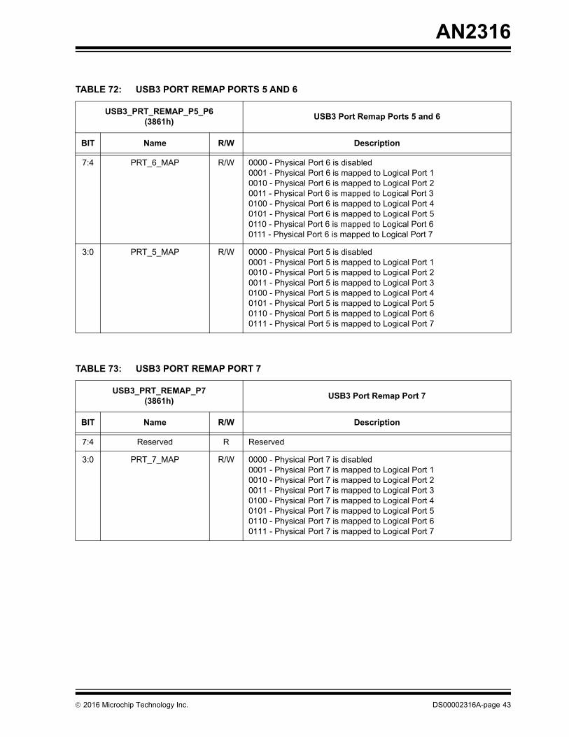
TABLE 72: USB3 PORT REMAP PORTS 5 AND 6
USB3_PRT_REMAP_P5_P6(3861h)
USB3 Port Remap Ports 5 and 6
BIT Name R/W Description
7:4 PRT_6_MAP R/W 0000 - Physical Port 6 is disabled0001 - Physical Port 6 is mapped to Logical Port 10010 - Physical Port 6 is mapped to Logical Port 20011 - Physical Port 6 is mapped to Logical Port 30100 - Physical Port 6 is mapped to Logical Port 40101 - Physical Port 6 is mapped to Logical Port 50110 - Physical Port 6 is mapped to Logical Port 60111 - Physical Port 6 is mapped to Logical Port 7
3:0 PRT_5_MAP R/W 0000 - Physical Port 5 is disabled0001 - Physical Port 5 is mapped to Logical Port 10010 - Physical Port 5 is mapped to Logical Port 20011 - Physical Port 5 is mapped to Logical Port 30100 - Physical Port 5 is mapped to Logical Port 40101 - Physical Port 5 is mapped to Logical Port 50110 - Physical Port 5 is mapped to Logical Port 60111 - Physical Port 5 is mapped to Logical Port 7
TABLE 73: USB3 PORT REMAP PORT 7
USB3_PRT_REMAP_P7(3861h)
USB3 Port Remap Port 7
BIT Name R/W Description
7:4 Reserved R Reserved
3:0 PRT_7_MAP R/W 0000 - Physical Port 7 is disabled0001 - Physical Port 7 is mapped to Logical Port 10010 - Physical Port 7 is mapped to Logical Port 20011 - Physical Port 7 is mapped to Logical Port 30100 - Physical Port 7 is mapped to Logical Port 40101 - Physical Port 7 is mapped to Logical Port 50110 - Physical Port 7 is mapped to Logical Port 60111 - Physical Port 7 is mapped to Logical Port 7
2016 Microchip Technology Inc. DS00002316A-page 43

AN2316
TABLE 74: USB 3.0 LINK LOW POWER STATE 1
LINK_PWR_STATE1(3870h)
USB 3.0 Link Low Power State 1
BIT Name R/W Description
7:6 P_STATE3 R Indicates state of downstream PHY3.
00 - U0 Normal Operation.01 - U1 Low recovery time latency.10 - U2 Longer recovery time latency.11 - U3 Lowest power state.
5:4 P_STATE2 R Indicates state of downstream PHY2.
00 - U0 Normal Operation.01 - U1 Low recovery time latency.10 - U2 Longer recovery time latency.11 - U3 Lowest power state.
3:2 P_STATE1 R Indicates state of downstream PHY1.
00 - U0 Normal Operation.01 - U1 Low recovery time latency.10 - U2 Longer recovery time latency.11 - U3 Lowest power state.
1:0 P_STATE0 R Indicates state of the upstream PHY.
00 - U0 Normal Operation.01 - U1 Low recovery time latency.10 - U2 Longer recovery time latency.11 - U3 Lowest power state.
TABLE 75: USB 3.0 LINK LOW POWER STATE 2
LINK_PWR_STATE2(3874h)
USB 3.0 Link Low Power State 2
BIT Name R/W Description
7:6 P_STATE7 R Indicates state of downstream PHY7.
00 - U0 Normal Operation.01 - U1 Low recovery time latency.10 - U2 Longer recovery time latency.11 - U3 Lowest power state.
5:4 P_STATE6 R Indicates state of downstream PHY6.
00 - U0 Normal Operation.01 - U1 Low recovery time latency.10 - U2 Longer recovery time latency.11 - U3 Lowest power state.
DS00002316A-page 44 2016 Microchip Technology Inc.

AN2316
3:2 P_STATE5 R Indicates state of downstream PHY5.
00 - U0 Normal Operation.01 - U1 Low recovery time latency.10 - U2 Longer recovery time latency.11 - U3 Lowest power state.
1:0 P_STATE4 R Indicates state of downstream PHY4.
00 - U0 Normal Operation.01 - U1 Low recovery time latency.10 - U2 Longer recovery time latency.11 - U3 Lowest power state.
TABLE 76: USB 3.1 GEN 1 PORT 1 CONFIGURATION SELECT
USB3_PRT_CFG_SEL1(3C00h)
Port 1 Configuration Select
BIT Name R/W Description
7 Reserved R Reserved. Should always be set to ‘1’.
6 GANG_PIN R/W When this bit is set, the port will be connected to the GANG_PWR pin.
5 DISABLED R/W When set, this bit disables the port.
Note: If this register is modified, the number of total USB 3.0 ports must be updated in . The USB 2.0 Equivalent must also be configured in the USB 2.0 Port 1 / Port 2 Remap register.
4 PERMANENT R/W When set, this bit indicates this port has a permanently attached device.
3:0 Reserved R This selects the source for the port power for portN.
0000b - Port Power is disabled for this Port.0001b - Port is on if USB2 port power is on.0010b - Port is on if USB3 port power is on.0011 - Port is on if USB2 or USB3 port power is on.0100b - Port is on if designated GPIO is on.All other values are reserved.
TABLE 75: USB 3.0 LINK LOW POWER STATE 2 (CONTINUED)
LINK_PWR_STATE2(3874h)
USB 3.0 Link Low Power State 2
BIT Name R/W Description
2016 Microchip Technology Inc. DS00002316A-page 45

AN2316
TABLE 77: USB 3.1 GEN 1 PORT 2 CONFIGURATION SELECT
USB3_PRT_CFG_SEL2(3C04h)
Port 2 Configuration Select
BIT Name R/W Description
7 Reserved R/W Reserved. Should always be set to ‘1’.
6 GANG_PIN R/W When this bit is set, the port will be connected to the GANG_PWR pin.
5 DISABLED R/W When set, this bit disables the port.
Note: If this register is modified, the number of total USB 3.0 ports must be updated in . The USB 2.0 Equivalent must also be configured in the USB 2.0 Port 1 / Port 2 Remap register.
4 PERMANENT R/W When set, this bit indicates this port has a permanently attached device.
3:0 Reserved R This selects the source for the port power for portN.
0000b - Port Power is disabled for this Port.0001b - Port is on if USB2 port power is on.0010b - Port is on if USB3 port power is on.0011 - Port is on if USB2 or USB3 port power is on.0100b - Port is on if designated GPIO is on.All other values are reserved.
TABLE 78: USB 3.1 GEN 1 PORT 3 CONFIGURATION SELECT
USB3_PRT_CFG_SEL3(3C08h)
Port 3 Configuration Select
BIT Name R/W Description
7 Reserved R Reserved. Should always be set to ‘1’.
6 GANG_PIN R/W When this bit is set, the port will be connected to the GANG_PWR pin.
5 DISABLED R/W When set, this bit disables the port.
Note: If this register is modified, the number of total USB 3.0 ports must be updated in . The USB 2.0 Equivalent must also be configured in the USB 2.0 Port 3 / Port 4 Remap register.
4 PERMANENT R/W When set, this bit indicates this port has a permanently attached device.
DS00002316A-page 46 2016 Microchip Technology Inc.

AN2316
3:0 Reserved R This selects the source for the port power for portN.
0000b - Port Power is disabled for this Port.0001b - Port is on if USB2 port power is on.0010b - Port is on if USB3 port power is on.0011 - Port is on if USB2 or USB3 port power is on.0100b - Port is on if designated GPIO is on.All other values are reserved..
TABLE 79: USB 3.1 GEN 1 PORT 4 CONFIGURATION SELECT
USB3_PRT_CFG_SEL4(3C0Ch)
Port 4 Configuration Select
BIT Name R/W Description
7 Reserved R Reserved. Should always be set to ‘1’.
6 GANG_PIN R/W When this bit is set, the port will be connected to the GANG_PWR pin.
5 DISABLED R/W When set, this bit disables the port.
Note: If this register is modified, the number of total USB 3.0 ports must be updated in . The USB 2.0 Equivalent must also be configured in the USB 2.0 Port 3 / Port 4 Remap register.
4 PERMANENT R/W When set, this bit indicates this port has a permanently attached device.
3:0 Reserved R This selects the source for the port power for portN.
0000b - Port Power is disabled for this Port.0001b - Port is on if USB2 port power is on.0010b - Port is on if USB3 port power is on.0011 - Port is on if USB2 or USB3 port power is on.0100b - Port is on if designated GPIO is on.All other values are reserved.
TABLE 78: USB 3.1 GEN 1 PORT 3 CONFIGURATION SELECT (CONTINUED)
USB3_PRT_CFG_SEL3(3C08h)
Port 3 Configuration Select
BIT Name R/W Description
2016 Microchip Technology Inc. DS00002316A-page 47

AN2316
TABLE 80: USB 3.1 GEN 1 PORT 5 CONFIGURATION SELECT
USB3_PRT_CFG_SEL5(3C10h)
Port 5 Configuration Select
BIT Name R/W Description
7 Reserved R Reserved. Should always be set to ‘1’.
6 GANG_PIN R/W When this bit is set, the port will be connected to the GANG_PWR pin.
5 DISABLED R/W When set, this bit disables the port.
Note: If this register is modified, the number of total USB 3.0 ports must be updated in . The USB 2.0 Equivalent must also be configured in the USB 2.0 Port 3 / Port 4 Remap register.
4 PERMANENT R/W When set, this bit indicates this port has a permanently attached device.
3:0 Reserved R This selects the source for the port power for portN.
0000b - Port Power is disabled for this Port.0001b - Port is on if USB2 port power is on.0010b - Port is on if USB3 port power is on.0011 - Port is on if USB2 or USB3 port power is on.0100b - Port is on if designated GPIO is on.All other values are reserved.
TABLE 81: USB 3.1 GEN 1 PORT 6 CONFIGURATION SELECT
USB3_PRT_CFG_SEL6(3C14h)
Port 6 Configuration Select
BIT Name R/W Description
7 Reserved R Reserved. Should always be set to ‘1’.
6 GANG_PIN R/W When this bit is set, the port will be connected to the GANG_PWR pin.
5 DISABLED R/W When set, this bit disables the port.
Note: If this register is modified, the number of total USB 3.0 ports must be updated in . The USB 2.0 Equivalent must also be configured in the USB 2.0 Port 3 / Port 4 Remap register.
4 PERMANENT R/W When set, this bit indicates this port has a permanently attached device.
DS00002316A-page 48 2016 Microchip Technology Inc.

AN2316
3:0 Reserved R This selects the source for the port power for portN.
0000b - Port Power is disabled for this Port.0001b - Port is on if USB2 port power is on.0010b - Port is on if USB3 port power is on.0011 - Port is on if USB2 or USB3 port power is on.0100b - Port is on if designated GPIO is on.All other values are reserved.
TABLE 82: USB 3.1 GEN 1 PORT 7 CONFIGURATION SELECT
USB3_PRT_CFG_SEL7(3C18h)
Port 7 Configuration Select
BIT Name R/W Description
7 Reserved R Reserved. Should always be set to ‘1’.
6 GANG_PIN R/W When this bit is set, the port will be connected to the GANG_PWR pin.
5 DISABLED R/W When set, this bit disables the port.
Note: If this register is modified, the number of total USB 3.0 ports must be updated in USB 3.0 Number of Ports. The USB 2.0 Equivalent must also be configured in the USB 2.0 Port 3 / Port 4 Remap register.
4 PERMANENT R/W When set, this bit indicates this port has a permanently attached device.
3:0 Reserved R This selects the source for the port power for portN.
0000b - Port Power is disabled for this Port.0001b - Port is on if USB2 port power is on.0010b - Port is on if USB3 port power is on.0011 - Port is on if USB2 or USB3 port power is on.0100b - Port is on if designated GPIO is on.All other values are reserved.
TABLE 81: USB 3.1 GEN 1 PORT 6 CONFIGURATION SELECT (CONTINUED)
USB3_PRT_CFG_SEL6(3C14h)
Port 6 Configuration Select
BIT Name R/W Description
2016 Microchip Technology Inc. DS00002316A-page 49

AN2316
TABLE 83: PORT 1 OVERCURRENT SENSE SOURCE SELECT
OCS_SEL1(3C20h)
Port 1 OCS Source Select
BIT Name R/W Description
7:5 Reserved R Always ‘0’
3:0 PRT_SEL R/W This selects the source for the port power for port 1:.0000b - The port is disabled.0001b - OCS comes from OCS pin.0010b - Reserved.0011b - OCS comes from GANG_PWR pin.1111b - Reserved.All other values are reserved.
TABLE 84: PORT 1 OVERCURRENT SENSE SOURCE SELECT
OCS_SEL1(3C20h)
Port 1 OCS Source Select
BIT Name R/W Description
7:5 Reserved R Always ‘0’
3:0 PRT_SEL R/W This selects the source for the port power for port 1:.0000b - The port is disabled.0001b - OCS comes from OCS pin.0010b - Reserved.0011b - OCS comes from GANG_PWR pin.1111b - Reserved.All other values are reserved.
TABLE 85: PORT 1 OVERCURRENT SENSE SOURCE SELECT
OCS_SEL1(3C20h)
Port 1 OCS Source Select
BIT Name R/W Description
7:5 Reserved R Always ‘0’
3:0 PRT_SEL R/W This selects the source for the port power for port 1:.0000b - The port is disabled.0001b - OCS comes from OCS pin.0010b - Reserved.0011b - OCS comes from GANG_PWR pin.1111b - Reserved.All other values are reserved.
DS00002316A-page 50 2016 Microchip Technology Inc.

AN2316
TABLE 86: PORT 2 OVERCURRENT SENSE SOURCE SELECT
OCS_SEL2(3C24h)
Port 2 OCS Source Select
BIT Name R/W Description
7:5 Reserved R Always ‘0’
3:0 PRT_SEL R/W This selects the source for the port power for port 2.0000b - The port is disabled.0001b - OCS comes from OCS pin.0010b - Reserved.0011b - OCS comes from GANG_PWR pin.1111b - Reserved.All other values are reserved.
TABLE 87: PORT 3 OVERCURRENT SENSE SOURCE SELECT
OCS_SEL3(3C28h)
Port 3 OCS Source Select
BIT Name R/W Description
7:5 Reserved R Always ‘0’
3:0 PRT_SEL R/W This selects the source for the port power for port 3.0000b - The port is disabled.0001b - OCS comes from OCS pin.0010b - Reserved.0011b - OCS comes from GANG_PWR pin.1111b - Reserved.All other values are reserved.
TABLE 88: PORT 4 OVERCURRENT SENSE SOURCE SELECT
OCS_SEL4(3C2Ah)
Port 4 OCS Source Select
BIT Name R/W Description
7:5 Reserved R Always ‘0’
3:0 PRT_SEL R/W This selects the source for the port power for port 4.0000b - The port is disabled.0001b - OCS comes from OCS pin.0010b - Reserved.0011b - OCS comes from GANG_PWR pin.1111b - Reserved.All other values are reserved.
2016 Microchip Technology Inc. DS00002316A-page 51

AN2316
TABLE 89: PORT 5 OVERCURRENT SENSE SOURCE SELECT
OCS_SEL5(3C30h)
Port 5 OCS Source Select
BIT Name R/W Description
7:5 Reserved R Always ‘0’
3:0 PRT_SEL R/W This selects the source for the port power for port 4.0000b - The port is disabled.0001b - OCS comes from OCS pin.0010b - Reserved.0011b - OCS comes from GANG_PWR pin.1111b - Reserved.All other values are reserved.
TABLE 90: PORT 6 OVERCURRENT SENSE SOURCE SELECT
OCS_SEL6(3C34h)
Port 6 OCS Source Select
BIT Name R/W Description
7:5 Reserved R Always ‘0’
3:0 PRT_SEL R/W This selects the source for the port power for port 4.0000b - The port is disabled.0001b - OCS comes from OCS pin.0010b - Reserved.0011b - OCS comes from GANG_PWR pin.1111b - Reserved.All other values are reserved.
TABLE 91: PORT 7 OVERCURRENT SENSE SOURCE SELECT
OCS_SEL4(3C38h)
Port 7 OCS Source Select
BIT Name R/W Description
7:5 Reserved R Always ‘0’
3:0 PRT_SEL R/W This selects the source for the port power for port 4.0000b - The port is disabled.0001b - OCS comes from OCS pin.0010b - Reserved.0011b - OCS comes from GANG_PWR pin.1111b - Reserved.All other values are reserved.
DS00002316A-page 52 2016 Microchip Technology Inc.

AN2316
TABLE 92: FLEXCONNECT CONFIGURATION 1
FLEX_CFG1(411Ah)
FlexConnect Configuration 1
BIT Name R/W Description
7 CHNG_PIN_FUNCT R/W This bit will change the digital pin controls back to the default states. For example, VBUS_DET has the same functionality regardless of the FLEX state.
6 FLEXCONNECT R/W The value of FLEXCONNECT after the Hub is re-attached
5 DIS_P5 R/W Disabled internal Hub Controller on port 5 after entering the “flexed” state. If this disabled, then no commands can be sent to the Hub Con-troller when in the “flexed” state.
4 DIS_P4 R/W Disabled downstream port 4 after switching directions.
3 DIS_P3 R/W Disabled downstream port 3 after switching directions.
2 DIS_P2 R/W Disabled downstream port 2 after switching directions.
1 DIS_P1 R/W Disabled downstream port 1 after switching directions.
0 Reserved R Reserved
TABLE 93: FLEXCONNECT CONFIGURATION 2
FLEX_CFG2(411Bh)
FlexConnect Configuration 2
BIT Name R/W Description
7 Reserved R Reserved. This bit must always read ‘1’.
6 DCP_EN R/W Enables the universal dedicated charging algorithm to be used on dis-abled ports. This will cause the hub to enumerate limited ports, but the VBUS and battery charging handshake will still be present on the dis-abled ports.
3:5 Reserved R Reserved
0:2 HD_TIMER R/W Host Detect Timeout - The time the hub will wait for a Host to enumer-ate before returning to the default state.
000 = No timeout001 = 10ms010 = 100ms011 = 500ms100 = 1s101 = 5s110 = 10s111 = 20s
2016 Microchip Technology Inc. DS00002316A-page 53

AN2316
TABLE 94: HUB FEATURE CONTROLLER ENABLE
HFC_ENABLE(4130h)
Hub Feature Controller Enable Register
BIT Name R/W Description
7:3 Reserved R Reserved
2:0 HFC_ENABLE_DISABLE R/W Allows Hub Feature Controller to be disabled
00b - Default behavior (disabled for USB5807, enabled for USB5806/USB5816/USB5826/USB5906/USB5916/USB5926)01b - Always enable Hub Feature Controller enumeration10b - Always disable Hub Feature Controller enumeration
TABLE 95: BILLBOARD DETACH TIMER A LSB
DETACH_TIMER_A_LSB(413Ch)
Billboard Detach Timer A LSB
BIT Name R/W Description
7:0 TIMEOUT R/W Note: This feature is only supported on USB5806, USB5816, USB5826, USB5906, USB5916, and USB5926 devices.
Timer A is started as soon as the Hub Feature Controller’s Billboard Class Device is set by the host. Once this timer expires, the Billboard Class Device will automatically detach from the host and re-attach as the default WinUSB device.
Increments of 10ms can be set.
The default value of 413Ch = D0h, 413Dh = 07h, the equivalent to a 20s timeout (07D0h = 2000d)
Note: Do not attempt to enable the Hub Feature Controller on hub devices with seven total downstream ports (i.e.: USB58xx/USB59xx part numbers ending in ‘7’ such as USB5807).
DS00002316A-page 54 2016 Microchip Technology Inc.

AN2316
TABLE 96: BILLBOARD DETACH TIMER A MSB
DETACH_TIMER_A_MSB(413Dh)
Billboard Detach Timer A MSB
BIT Name R/W Description
7:0 TIMEOUT R/W Note: This feature is only supported on USB5806, USB5816, USB5826, USB5906, USB5916, and USB5926 devices.
Timer A is started as soon as the Hub Feature Controller’s Billboard Class Device is set by the host. Once this timer expires, the Billboard Class Device will automatically detach from the host and re-attach as the default WinUSB device.
Increments of 10ms can be set.
The default value of 413Ch = D0h, 413Dh = 07h, the equivalent to a 20s timeout (07D0h = 2000d)
TABLE 97: BILLBOARD DETACH TIMER B LSB
DETACH_TIMER_B_LSB(413Eh)
Billboard Detach Timer B LSB
BIT Name R/W Description
7:0 TIMEOUT R/W Note: This feature is only supported on USB5806, USB5816, USB5826, USB5906, USB5916, and USB5926 devices.
Timer B is started as soon as the host requests iAlternateModeString. Once the timer expires, the Billboard Class Device will automatically detach from the host and re-attach as the default WinUSB device.
Increments of 10ms can be set.
The default value of 413Eh = D0h, 413Fh = 07h, the equivalent to a 20s timeout (07D0h = 2000d)
2016 Microchip Technology Inc. DS00002316A-page 55

AN2316
TABLE 98: BILLBOARD DETACH TIMER B MSB
DETACH_TIMER_B_MSB(413Eh)
Billboard Detach Timer B MSB
BIT Name R/W Description
7:0 TIMEOUT R/W Note: This feature is only supported on USB5806, USB5816, USB5826, USB5906, USB5916, and USB5926 devices.
Timer B is started as soon as the host requests iAlternateModeString. Once the timer expires, the Billboard Class Device will automatically detach from the host and re-attach as the default WinUSB device.
Increments of 10ms can be set.
The default value of 413Eh = D0h, 413Fh = 07h, the equivalent to a 20s timeout (07D0h = 2000d)
TABLE 99: PORT SPLIT PRTPWRX_USB3_SPLIT CONTROL SELECT 1
PORT_SPLIT_A_SELECT(416Dh)
Port Split PRTPWR Control Select Register 1
BIT Name R/W Description
7:0 PORT_SPLIT_A_SE-LECT
R/W Note: Each device has slight differences in Port Split implementa-tion.See product datasheet for details on Port Split imple-mentation for the specific device.
Up to two ports can be configured to operate in Port Split mode.
This register selects which GPIO to assign the role of the PRTPWRx-_USB3_SPLIT for the first Port Split port.
0100 0010 = Select GPIO660000 0101 = Select GPIO5All others - Reserved
DS00002316A-page 56 2016 Microchip Technology Inc.
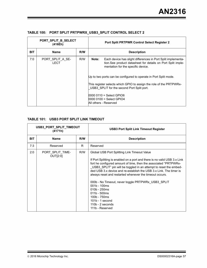
AN2316
TABLE 100: PORT SPLIT PRTPWRX_USB3_SPLIT CONTROL SELECT 2
PORT_SPLIT_B_SELECT(416Eh)
Port Split PRTPWR Control Select Register 2
BIT Name R/W Description
7:0 PORT_SPLIT_A_SE-LECT
R/W Note: Each device has slight differences in Port Split implementa-tion.See product datasheet for details on Port Split imple-mentation for the specific device.
Up to two ports can be configured to operate in Port Split mode.
This register selects which GPIO to assign the role of the PRTPWRx-_USB3_SPLIT for the second Port Split port.
0000 0110 = Select GPIO60000 0100 = Select GPIO4All others - Reserved
TABLE 101: USB3 PORT SPLIT LINK TIMEOUT
USB3_PORT_SPLIT_TIMEOUT(4171h)
USB3 Port Split Link Timeout Register
BIT Name R/W Description
7:3 Reserved R Reserved
2:0 PORT_SPLIT_TIME-OUT[2:0]
R/W Global USB Port Splitting Link Timeout Value
If Port Splitting is enabled on a port and there is no valid USB 3.x Link fort he configured amount of time, then the associated “PRTPWRx-_USB3_SPLIT” pin will be toggled in an attempt to reset the embed-ded USB 3.x device and re-establish the USB 3.x Link. The timer is always reset and restarted whenever the timeout occurs.
000b - No Timeout, never toggle PRTPWRx_USB3_SPLIT001b - 100ms010b - 250ms011b - 500ms100b - 750ms101b - 1 second110b - 2 seconds111b - Reserved
2016 Microchip Technology Inc. DS00002316A-page 57

AN2316
TABLE 102: USB3 PORT SPLIT TOGGLE TIME
USB3_PORT_SPLIT_TOGGLE_TIME(4176h)
USB3 Port Split Toggle Time Register
BIT Name R/W Description
7:0 PORT_SPLIT_TIME-OUT[7:0]
R/W The PORT_SPLIT_TOGGLE_TIME is used to control the length of the time port power is toggled off. This is specific to the “PRTPWRx-_USB3_SPLIT” pin, and is only used in conjunction with register 4171h. The timer is always reset whenever the toggle completes.
The minimum toggle time is 350ms and is represented by 0000 0000b.
Each incremental value will add 10ms to the 350ms minimum value.
TABLE 103: BATTERY CHARGING PORT 1 CONFIGURATION
BC_CFG_P1(4178h)
Battery Charging Port 1 Configuration
BIT Name R/W Description
7 BCDCP_DIS_PRTS_EN R/W 1 - When this port is disabled, DCP mode will be enabled on this port. The mode of operation will be determined from Bits 5:0 of this register
0 - When the port is disabled, DCP mode will not be enabled
6 Reserved R Reserved
5 BC12_CDCP R/W When set, enables BC 1.2 DCP mode. If Bit 4 is set, this bit will be ignored.
4 CHINA R/W When set, enables China mode.
3 Reserved R Reserved
2:1 SE1_MODE R/W SE1 mode sets the DP/DM signals to static voltages for charging cer-tain devices that do not follow the BC1.2 standard.
00 - SE1 Mode is disabled.01 - SE1 1 A Mode. DP = 2.0V, DM = 2.7V10 - SE1 2 A Mode. DP = 2.7V, DM = 2.0V11 - SE1 2.5 A Mode. DP = DM = 2.7V
Note: When both SE1 mode and BC1.2 modes are enabled, the port will automatically switch between the two modes of operation when a device is connected in order to supply the appropriate handshake for the device. See the battery charging section in the datasheet for additional details.
0 BC_EN R/W 1 - Enables Battery Charging on port 1.0 - Disables Battery Charging on port 1.
DS00002316A-page 58 2016 Microchip Technology Inc.

AN2316
TABLE 104: BATTERY CHARGING PORT 2 CONFIGURATION
BC_CFG_P2(4179h)
Battery Charging Port 2 Configuration
BIT Name R/W Description
7 BCDCP_DIS_PRTS_EN R/W 1 - When this port is disabled, DCP mode will be enabled on this port. The mode of operation will be determined from Bits 5:0 of this register
0 - When the port is disabled, DCP mode will not be enabled
6 Reserved R Reserved
5 BC12_CDCP R/W When set, enables BC 1.2 DCP mode. If Bit 4 is set, this bit will be ignored.
4 CHINA R/W When set, enables China mode.
3 Reserved R Reserved
2:1 SE1_MODE R/W SE1 mode sets the DP/DM signals to static voltages for charging cer-tain devices that do not follow the BC1.2 standard.
00 - SE1 Mode is disabled.01 - SE1 1 A Mode. DP = 2.0V, DM = 2.7V10 - SE1 2 A Mode. DP = 2.7V, DM = 2.0V11 - SE1 2.5 A Mode. DP = DM = 2.7V
Note: When both SE1 mode and BC1.2 modes are enabled, the port will automatically switch between the two modes of operation when a device is connected in order to supply the appropriate handshake for the device. See the battery charging section in the datasheet for additional details.
0 BC_EN R/W 1 - Enables Battery Charging on port 2.0 - Disables Battery Charging on port 2.
TABLE 105: BATTERY CHARGING PORT 3 CONFIGURATION
BC_CFG_P3(417Ah)
Battery Charging Port 3 Configuration
BIT Name R/W Description
7 BCDCP_DIS_PRTS_EN R/W 1 - When this port is disabled, DCP mode will be enabled on this port. The mode of operation will be determined from Bits 5:0 of this register
0 - When the port is disabled, DCP mode will not be enabled
6 Reserved R Reserved
5 BC12_CDCP R/W When set, enables BC 1.2 DCP mode. If Bit 4 is set, this bit will be ignored.
4 CHINA R/W When set, enables China mode.
2016 Microchip Technology Inc. DS00002316A-page 59

AN2316
3 Reserved R Reserved
2:1 SE1_MODE R/W SE1 mode sets the DP/DM signals to static voltages for charging cer-tain devices that do not follow the BC1.2 standard.
00 - SE1 Mode is disabled.01 - SE1 1 A Mode. DP = 2.0V, DM = 2.7V10 - SE1 2 A Mode. DP = 2.7V, DM = 2.0V11 - SE1 2.5 A Mode. DP = DM = 2.7V
Note: When both SE1 mode and BC1.2 modes are enabled, the port will automatically switch between the two modes of operation when a device is connected in order to supply the appropriate handshake for the device. See the battery charging section in the datasheet for additional details.
0 BC_EN R/W 1 - Enables Battery Charging on port 3.0 - Disables Battery Charging on port 3.
TABLE 106: BATTERY CHARGING PORT 4 CONFIGURATION
BC_CFG_P4(417Bh)
Battery Charging Port 4 Configuration
BIT Name R/W Description
7 BCDCP_DIS_PRTS_EN R/W 1 - When this port is disabled, DCP mode will be enabled on this port. The mode of operation will be determined from Bits 5:0 of this register
0 - When the port is disabled, DCP mode will not be enabled
6 Reserved R Reserved
5 BC12_CDCP R/W When set, enables BC 1.2 DCP mode. If Bit 4 is set, this bit will be ignored.
4 CHINA R/W When set, enables China mode.
3 Reserved R Reserved
TABLE 105: BATTERY CHARGING PORT 3 CONFIGURATION (CONTINUED)
BC_CFG_P3(417Ah)
Battery Charging Port 3 Configuration
BIT Name R/W Description
DS00002316A-page 60 2016 Microchip Technology Inc.

AN2316
2:1 SE1_MODE R/W SE1 mode sets the DP/DM signals to static voltages for charging cer-tain devices that do not follow the BC1.2 standard.
00 - SE1 Mode is disabled.01 - SE1 1 A Mode. DP = 2.0V, DM = 2.7V10 - SE1 2 A Mode. DP = 2.7V, DM = 2.0V11 - SE1 2.5 A Mode. DP = DM = 2.7V
Note: When both SE1 mode and BC1.2 modes are enabled, the port will automatically switch between the two modes of operation when a device is connected in order to supply the appropriate handshake for the device. See the battery charging section in the datasheet for additional details.
0 BC_EN R/W 1 - Enables Battery Charging on port 4.0 - Disables Battery Charging on port 4.
TABLE 107: BATTERY CHARGING PORT 5 CONFIGURATION
BC_CFG_P5(417Ch)
Battery Charging Port 5 Configuration
BIT Name R/W Description
7 BCDCP_DIS_PRTS_EN R/W 1 - When this port is disabled, DCP mode will be enabled on this port. The mode of operation will be determined from Bits 5:0 of this register
0 - When the port is disabled, DCP mode will not be enabled
6 Reserved R Reserved
5 BC12_CDCP R/W When set, enables BC 1.2 DCP mode. If Bit 4 is set, this bit will be ignored.
4 CHINA R/W When set, enables China mode.
3 Reserved R Reserved
TABLE 106: BATTERY CHARGING PORT 4 CONFIGURATION (CONTINUED)
BC_CFG_P4(417Bh)
Battery Charging Port 4 Configuration
BIT Name R/W Description
2016 Microchip Technology Inc. DS00002316A-page 61

AN2316
2:1 SE1_MODE R/W SE1 mode sets the DP/DM signals to static voltages for charging cer-tain devices that do not follow the BC1.2 standard.
00 - SE1 Mode is disabled.01 - SE1 1 A Mode. DP = 2.0V, DM = 2.7V10 - SE1 2 A Mode. DP = 2.7V, DM = 2.0V11 - SE1 2.5 A Mode. DP = DM = 2.7V
Note: When both SE1 mode and BC1.2 modes are enabled, the port will automatically switch between the two modes of operation when a device is connected in order to supply the appropriate handshake for the device. See the battery charging section in the datasheet for additional details.
0 BC_EN R/W 1 - Enables Battery Charging on port 4.0 - Disables Battery Charging on port 4.
TABLE 108: BATTERY CHARGING PORT 6 CONFIGURATION
BC_CFG_P6(417Dh)
Battery Charging Port 6 Configuration
BIT Name R/W Description
7 BCDCP_DIS_PRTS_EN R/W 1 - When this port is disabled, DCP mode will be enabled on this port. The mode of operation will be determined from Bits 5:0 of this register
0 - When the port is disabled, DCP mode will not be enabled
6 Reserved R Reserved
5 BC12_CDCP R/W When set, enables BC 1.2 DCP mode. If Bit 4 is set, this bit will be ignored.
4 CHINA R/W When set, enables China mode.
3 Reserved R Reserved
TABLE 107: BATTERY CHARGING PORT 5 CONFIGURATION (CONTINUED)
BC_CFG_P5(417Ch)
Battery Charging Port 5 Configuration
BIT Name R/W Description
DS00002316A-page 62 2016 Microchip Technology Inc.

AN2316
2:1 SE1_MODE R/W SE1 mode sets the DP/DM signals to static voltages for charging cer-tain devices that do not follow the BC1.2 standard.
00 - SE1 Mode is disabled.01 - SE1 1 A Mode. DP = 2.0V, DM = 2.7V10 - SE1 2 A Mode. DP = 2.7V, DM = 2.0V11 - SE1 2.5 A Mode. DP = DM = 2.7V
Note: When both SE1 mode and BC1.2 modes are enabled, the port will automatically switch between the two modes of operation when a device is connected in order to supply the appropriate handshake for the device. See the battery charging section in the datasheet for additional details.
0 BC_EN R/W 1 - Enables Battery Charging on port 4.0 - Disables Battery Charging on port 4.
TABLE 109: BATTERY CHARGING PORT 7 CONFIGURATION
BC_CFG_P7(417Eh)
Battery Charging Port 7 Configuration
BIT Name R/W Description
7 BCDCP_DIS_PRTS_EN R/W 1 - When this port is disabled, DCP mode will be enabled on this port. The mode of operation will be determined from Bits 5:0 of this register
0 - When the port is disabled, DCP mode will not be enabled
6 Reserved R Reserved
5 BC12_CDCP R/W When set, enables BC 1.2 DCP mode. If Bit 4 is set, this bit will be ignored.
4 CHINA R/W When set, enables China mode.
3 Reserved R Reserved
TABLE 108: BATTERY CHARGING PORT 6 CONFIGURATION (CONTINUED)
BC_CFG_P6(417Dh)
Battery Charging Port 6 Configuration
BIT Name R/W Description
2016 Microchip Technology Inc. DS00002316A-page 63

AN2316
2:1 SE1_MODE R/W SE1 mode sets the DP/DM signals to static voltages for charging cer-tain devices that do not follow the BC1.2 standard.
00 - SE1 Mode is disabled.01 - SE1 1 A Mode. DP = 2.0V, DM = 2.7V10 - SE1 2 A Mode. DP = 2.7V, DM = 2.0V11 - SE1 2.5 A Mode. DP = DM = 2.7V
Note: When both SE1 mode and BC1.2 modes are enabled, the port will automatically switch between the two modes of operation when a device is connected in order to supply the appropriate handshake for the device. See the battery charging section in the datasheet for additional details.
0 BC_EN R/W 1 - Enables Battery Charging on port 4.0 - Disables Battery Charging on port 4.
TABLE 110: FLEXCONNECT CONTROL REGISTER
FLEX_CONTROL_REG(4177h)
Flex Control Register
BIT Name R/W Description
7 DISABLE_FLEX_INDICA-TOR
R/W ‘1’ - FLEX_STATE pin is used as GPIO72‘0’ - FLEX_STATE pin is used to indicate state of FLEXCONNECT
6 ENUM_TIMER_EN R/W ‘1’ - ENUM_TMP timer mechanism is enabled when FlexConnect is initiated.
‘0’ - ENUM_TMP timer mechanism is disabled
5 CAR_PLAY_APP R/W ‘1’ - Automotive Application Mode disabled. State of PRTCTL1 is con-trolled by Port 1 status (standard USB operation).
‘0’ - Automotive Application Mode enabled. When this mode is enabled, the PRTCTL1 pin is always driven high regardless of Port 1 status when FlexConnect mode is initiated.
4 DISABLE_GPIO_PER-SISTENCE
R/W ‘1’ - GPIO Persistance is disabled. All GPIOs that have been manually set by register writes via SMBus or USB command will reset to their default state after FlexConnect is initiated.
‘0’ - GPIO Persistance is enabled. All GPIOs that have been manually set by register writes via SMBus or USB command will maintain the same state after FlexConnect is initiated.
3 ENABLE_FLEX_BY_X-DATA_WRITE
R/W ‘1’ - Enable FlexConnect initiation through XDATA register writes.
‘0’ -Disable FlexConnect initiation through XDATA register writes.
TABLE 109: BATTERY CHARGING PORT 7 CONFIGURATION (CONTINUED)
BC_CFG_P7(417Eh)
Battery Charging Port 7 Configuration
BIT Name R/W Description
DS00002316A-page 64 2016 Microchip Technology Inc.
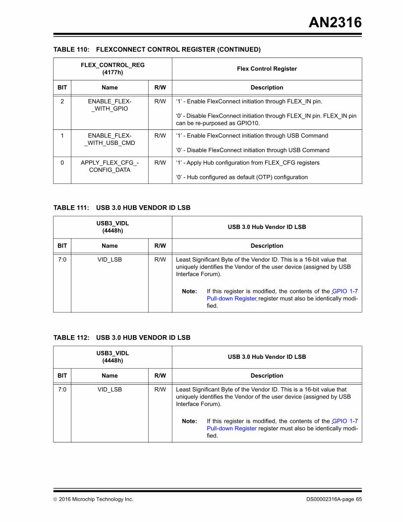
AN2316
2 ENABLE_FLEX-_WITH_GPIO
R/W ‘1’ - Enable FlexConnect initiation through FLEX_IN pin.
‘0’ - Disable FlexConnect initiation through FLEX_IN pin. FLEX_IN pin can be re-purposed as GPIO10.
1 ENABLE_FLEX-_WITH_USB_CMD
R/W ‘1’ - Enable FlexConnect initiation through USB Command
‘0’ - Disable FlexConnect initiation through USB Command
0 APPLY_FLEX_CFG_-CONFIG_DATA
R/W ‘1’ - Apply Hub configuration from FLEX_CFG registers
‘0’ - Hub configured as default (OTP) configuration
TABLE 111: USB 3.0 HUB VENDOR ID LSB
USB3_VIDL(4448h)
USB 3.0 Hub Vendor ID LSB
BIT Name R/W Description
7:0 VID_LSB R/W Least Significant Byte of the Vendor ID. This is a 16-bit value thatuniquely identifies the Vendor of the user device (assigned by USB Interface Forum).
TABLE 112: USB 3.0 HUB VENDOR ID LSB
USB3_VIDL(4448h)
USB 3.0 Hub Vendor ID LSB
BIT Name R/W Description
7:0 VID_LSB R/W Least Significant Byte of the Vendor ID. This is a 16-bit value thatuniquely identifies the Vendor of the user device (assigned by USB Interface Forum).
Note: If this register is modified, the contents of the GPIO 1-7 Pull-down Register register must also be identically modi-fied.
Note: If this register is modified, the contents of the GPIO 1-7 Pull-down Register register must also be identically modi-fied.
TABLE 110: FLEXCONNECT CONTROL REGISTER (CONTINUED)
FLEX_CONTROL_REG(4177h)
Flex Control Register
BIT Name R/W Description
2016 Microchip Technology Inc. DS00002316A-page 65

AN2316
TABLE 113: USB 3.0 HUB VENDOR ID MSB
USB3_VIDM(4449h)
USB 3.0 Hub Vendor ID MSB
BIT Name R/W Description
7:0 VID_MSB R/W Most Significant Byte of the Vendor ID. This is a 16-bit value thatuniquely identifies the Vendor of the user device (assigned by USB Interface Forum).
TABLE 114: USB 3.0 HUB PRODUCT ID LSB
USB3_PIDL(444Ah)
USB 3.0 Hub Product ID LSB
BIT Name R/W Description
7:0 PID_LSB R/W Least Significant Byte of the Product ID. This is a 16-bit value that the Vendor can assign to uniquely identify this particular product (assigned by OEM).
TABLE 115: USB 3.0 HUB PRODUCT ID MSB
USB3_PIDM(444Bh)
USB 3.0 Hub Product ID MSB
BIT Name R/W Description
7:0 PID_MSB R/W Most Significant Byte of the Product ID. This is a 16-bit value that the Vendor can assign to uniquely identify this particular product (assigned by OEM).
TABLE 116: USB 3.0 HUB DEVICE ID LSB
USB3_DIDL(444Ch)
USB 3.0 Hub Product ID LSB
BIT Name R/W Description
7:0 DID_LSB R/W Least Significant Byte of the Device ID. This is a 16-bit device release number in BCD format (assigned by OEM).
Note: If this register is modified, the contents of the USB 2.0 Hub Vendor ID MSB register must also be identically modified.
DS00002316A-page 66 2016 Microchip Technology Inc.

AN2316
TABLE 117: USB 3.0 HUB DEVICE ID MSB
USB3_DIDM(444Dh)
USB 3.0 Hub Product ID MSB
BIT Name R/W Description
7:0 DID_MSB R/W Most Significant Byte of the Device ID. This is a 16-bit device release number in BCD format (assigned by OEM).
.
TABLE 118: USB 3.0 NUMBER OF PORTS
USB3_NBR_PRTS(44A2h)
USB 3.0 Number of Ports
BIT Name R/W Description
7:3 Reserved R Reserved
0:3 Number of Ports R/W 111 = 7 Ports Enabled110 = 6 Ports Enabled101 = 5 Ports Enabled100 = 4 Ports Enabled011 = 3 Ports Enabled010 = 2 Ports Enabled001 = 1 Port Enabled000 = No Ports Enabled
Note: If this register is modified, the specific USB 3.0 ports must be disabled in If this register is modified, the USB 2.0 Hub equivalent must also be modified in the USB 3.1 Gen 1 Port 1 Configuration Select, USB 3.1 Gen 1 Port 2 Config-uration Select , USB 3.1 Gen 1 Port 3 Configuration Select, and USB 3.1 Gen 1 Port 4 Configuration Select registers. The USB 2.0 Equivalent must also be configured in the USB 2.0 Port 1 / Port 2 Remap and USB 2.0 Port 3 / Port 4 Remap registers.
TABLE 119: USB 3.0 HUB COMPOUND DEVICE
USB3_COMPOUND(44A3h)
USB 3.0 Hub Compound Device
BIT Name R/W Description
7:3 Reserved R Reserved
2 COMPOUND_DEVICE R/W 0 = Hub is not part of a Compound Device1 = Hus is part of a Compound Device
If this register is modified, the USB 2.0 Hub equivalent must also be modified in the USB 2.0 Hub Configuration 2 register.
2016 Microchip Technology Inc. DS00002316A-page 67

AN2316
1:0 Reserved R Reserved
TABLE 120: USB 3.0 HUB NON REMOVABLE DEVICE
USB3_NRD(44AAh)
USB 3.0 Hub Non-Removable Device
BIT Name R/W Description
7:1 NR_DEVICE R/W Non-Removable Device: Indicates which port(s) include non- remov-able devices. ‘0’ = port is removable, ‘1’ = port is non- removable.Informs the Host if one of the active ports has a permanent device that is undetachable from the Hub.
The ports may also be configured as Non-Removable using the hard-ware strapping option described in section 3.4.3 of the USB57x4 datasheet.
Bit 7 = 1; Port 7 non-removable.Bit 6 = 1; Port 6 non-removable.Bit 5 = 1; Port 5 non-removable.Bit 4 = 1; Port 4 non-removable.Bit 3 = 1; Port 3 non-removable.Bit 2 = 1; Port 2 non-removable.Bit 1 = 1; Port 1 non removable.
If this register is modified, the USB 2.0 Hub equivalent must also be modified in the register.
0 Reserved R Reserved
TABLE 121: USB 2.0 UPSTREAM PHYBOOST REGISTER
HS_UP_BOOST(60CAh)
USB 2.0 Upstream PHYBoost Register
BIT Name R/W Description
7:3 Reserved R Reserved
TABLE 119: USB 3.0 HUB COMPOUND DEVICE (CONTINUED)
USB3_COMPOUND(44A3h)
USB 3.0 Hub Compound Device
BIT Name R/W Description
DS00002316A-page 68 2016 Microchip Technology Inc.

AN2316
2:0 HS_BOOST R/W HS Output Current Adjustment
000b: Nominal001b: Decrease by 5%00b: Increase by 10%011b: Increase by 5%100b: Increase by 20%101b: Increase by 15%110b: Increase by 30%111b: Increase by 25%
TABLE 122: USB 2.0 UPSTREAM VARISENSE REGISTER
HS_UP_SENSE(60CCh)
USB 2.0 Upstream VariSense Register
BIT Name R/W Description
7:3 Reserved R Reserved
2:0 HS_SENSE R/W HS VariSense Tune (Squelch Tune)
000b: Nominal (100 mV Trip Point)001b: Decrease by 12.5 mV00b: Decrease by 25 mV011b: Decrease by 37.5 mV100b: Decrease by 50 mV101b: Decrease by 62.5 mV110b: Increase by 25 mV111b: Increase by 12.5 mV
TABLE 123: USB 2.0 DOWNSTREAM PORT 1 PHYBOOST REGISTER
HS_P1_BOOST(64CAh)
USB 2.0 Downstream Port 1 PHYBoost Register
BIT Name R/W Description
7:3 Reserved R Reserved
TABLE 121: USB 2.0 UPSTREAM PHYBOOST REGISTER (CONTINUED)
HS_UP_BOOST(60CAh)
USB 2.0 Upstream PHYBoost Register
BIT Name R/W Description
2016 Microchip Technology Inc. DS00002316A-page 69

AN2316
2:0 HS_BOOST R/W HS Output Current Adjustment
000b: Nominal001b: Decrease by 5%00b: Increase by 10%011b: Increase by 5%100b: Increase by 20%101b: Increase by 15%110b: Increase by 30%111b: Increase by 25%
TABLE 124: USB 2.0 DOWNSTREAM PORT 1 VARISENSE REGISTER
HS_P1_SENSE(64CCh)
USB 2.0 Downstream Port 1 VariSense Register
BIT Name R/W Description
7:3 Reserved R Reserved
2:0 HS_SENSE R/W HS VariSense Tune (Squelch Tune)
000b: Nominal (100 mV Trip Point)001b: Decrease by 12.5 mV00b: Decrease by 25 mV011b: Decrease by 37.5 mV100b: Decrease by 50 mV101b: Decrease by 62.5 mV110b: Increase by 25 mV111b: Increase by 12.5 mV
TABLE 125: USB 2.0 DOWNSTREAM PORT2 PHYBOOST REGISTER
HS_P2_BOOST(64CAh)
USB 2.0 Downstream Port 2 PHYBoost Register
BIT Name R/W Description
7:3 Reserved R Reserved
TABLE 123: USB 2.0 DOWNSTREAM PORT 1 PHYBOOST REGISTER (CONTINUED)
HS_P1_BOOST(64CAh)
USB 2.0 Downstream Port 1 PHYBoost Register
BIT Name R/W Description
DS00002316A-page 70 2016 Microchip Technology Inc.

AN2316
2:0 HS_BOOST R/W HS Output Current Adjustment
000b: Nominal001b: Decrease by 5%00b: Increase by 10%011b: Increase by 5%100b: Increase by 20%101b: Increase by 15%110b: Increase by 30%111b: Increase by 25%
TABLE 126: USB 2.0 DOWNSTREAM PORT 2 VARISENSE REGISTER
HS_P2_SENSE(68CCh)
USB 2.0 Downstream Port 2 VariSense Register
BIT Name R/W Description
7:3 Reserved R Reserved
2:0 HS_SENSE R/W HS VariSense Tune (Squelch Tune)
000b: Nominal (100 mV Trip Point)001b: Decrease by 12.5 mV00b: Decrease by 25 mV011b: Decrease by 37.5 mV100b: Decrease by 50 mV101b: Decrease by 62.5 mV110b: Increase by 25 mV111b: Increase by 12.5 mV
TABLE 127: USB 2.0 DOWNSTREAM PORT 3 PHYBOOST REGISTER
HS_P3_BOOST(6CCAh)
USB 2.0 Downstream Port 3 PHYBoost Register
BIT Name R/W Description
7:3 Reserved R Reserved
TABLE 125: USB 2.0 DOWNSTREAM PORT2 PHYBOOST REGISTER (CONTINUED)
HS_P2_BOOST(64CAh)
USB 2.0 Downstream Port 2 PHYBoost Register
BIT Name R/W Description
2016 Microchip Technology Inc. DS00002316A-page 71

AN2316
2:0 HS_BOOST R/W HS Output Current Adjustment
000b: Nominal001b: Decrease by 5%00b: Increase by 10%011b: Increase by 5%100b: Increase by 20%101b: Increase by 15%110b: Increase by 30%111b: Increase by 25%
TABLE 128: USB 2.0 DOWNSTREAM PORT 3 VARISENSE REGISTER
HS_P3_SENSE(6CCCh)
USB 2.0 Downstream Port 3 VariSense Register
BIT Name R/W Description
7:3 Reserved R Reserved
2:0 HS_SENSE R/W HS VariSense Tune (Squelch Tune)
000b: Nominal (100 mV Trip Point)001b: Decrease by 12.5 mV00b: Decrease by 25 mV011b: Decrease by 37.5 mV100b: Decrease by 50 mV101b: Decrease by 62.5 mV110b: Increase by 25 mV111b: Increase by 12.5 mV
TABLE 129: USB 2.0 DOWNSTREAM PORT 4 PHYBOOST REGISTER
HS_P4_BOOST(70CAh)
USB 2.0 Downstream Port 4 PHYBoost Register
BIT Name R/W Description
7:3 Reserved R Reserved
TABLE 127: USB 2.0 DOWNSTREAM PORT 3 PHYBOOST REGISTER (CONTINUED)
HS_P3_BOOST(6CCAh)
USB 2.0 Downstream Port 3 PHYBoost Register
BIT Name R/W Description
DS00002316A-page 72 2016 Microchip Technology Inc.

AN2316
2:0 HS_BOOST R/W HS Output Current Adjustment
000b: Nominal001b: Decrease by 5%00b: Increase by 10%011b: Increase by 5%100b: Increase by 20%101b: Increase by 15%110b: Increase by 30%111b: Increase by 25%
TABLE 130: USB 2.0 DOWNSTREAM PORT 4 VARISENSE REGISTER
HS_P4_SENSE(70CCh)
USB 2.0 Downstream Port 4 VariSense Register
BIT Name R/W Description
7:3 Reserved R Reserved
2:0 HS_SENSE R/W HS VariSense Tune (Squelch Tune)
000b: Nominal (100 mV Trip Point)001b: Decrease by 12.5 mV00b: Decrease by 25 mV011b: Decrease by 37.5 mV100b: Decrease by 50 mV101b: Decrease by 62.5 mV110b: Increase by 25 mV111b: Increase by 12.5 mV
TABLE 129: USB 2.0 DOWNSTREAM PORT 4 PHYBOOST REGISTER (CONTINUED)
HS_P4_BOOST(70CAh)
USB 2.0 Downstream Port 4 PHYBoost Register
BIT Name R/W Description
2016 Microchip Technology Inc. DS00002316A-page 73

AN2316
TABLE 131: USB 2.0 DOWNSTREAM PORT 5 PHYBOOST REGISTER
HS_P5_BOOST(74CAh)
USB 2.0 Downstream Port 5 PHYBoost Register
BIT Name R/W Description
7:3 Reserved R Reserved
2:0 HS_BOOST R/W HS Output Current Adjustment
000b: Nominal001b: Decrease by 5%00b: Increase by 10%011b: Increase by 5%100b: Increase by 20%101b: Increase by 15%110b: Increase by 30%111b: Increase by 25%
TABLE 132: USB 2.0 DOWNSTREAM PORT 5 VARISENSE REGISTER
HS_P5_SENSE(74CCh)
USB 2.0 Downstream Port 5 VariSense Register
BIT Name R/W Description
7:3 Reserved R Reserved
2:0 HS_SENSE R/W HS VariSense Tune (Squelch Tune)
000b: Nominal (100 mV Trip Point)001b: Decrease by 12.5 mV00b: Decrease by 25 mV011b: Decrease by 37.5 mV100b: Decrease by 50 mV101b: Decrease by 62.5 mV110b: Increase by 25 mV111b: Increase by 12.5 mV
DS00002316A-page 74 2016 Microchip Technology Inc.

AN2316
TABLE 133: USB 2.0 DOWNSTREAM PORT 6 PHYBOOST REGISTER
HS_P6_BOOST(78CAh)
USB 2.0 Downstream Port 6 PHYBoost Register
BIT Name R/W Description
7:3 Reserved R Reserved
2:0 HS_BOOST R/W HS Output Current Adjustment
000b: Nominal001b: Decrease by 5%00b: Increase by 10%011b: Increase by 5%100b: Increase by 20%101b: Increase by 15%110b: Increase by 30%111b: Increase by 25%
TABLE 134: USB 2.0 DOWNSTREAM PORT 6 VARISENSE REGISTER
HS_P6_SENSE(78CCh)
USB 2.0 Downstream Port 6 VariSense Register
BIT Name R/W Description
7:3 Reserved R Reserved
2:0 HS_SENSE R/W HS VariSense Tune (Squelch Tune)
000b: Nominal (100 mV Trip Point)001b: Decrease by 12.5 mV00b: Decrease by 25 mV011b: Decrease by 37.5 mV100b: Decrease by 50 mV101b: Decrease by 62.5 mV110b: Increase by 25 mV111b: Increase by 12.5 mV
2016 Microchip Technology Inc. DS00002316A-page 75

AN2316
TABLE 135: USB 2.0 DOWNSTREAM PORT 7 PHYBOOST REGISTER
HS_P7_BOOST(7CCAh)
USB 2.0 Downstream Port 7 PHYBoost Register
BIT Name R/W Description
7:3 Reserved R Reserved
2:0 HS_BOOST R/W HS Output Current Adjustment
000b: Nominal001b: Decrease by 5%00b: Increase by 10%011b: Increase by 5%100b: Increase by 20%101b: Increase by 15%110b: Increase by 30%111b: Increase by 25%
TABLE 136: USB 2.0 DOWNSTREAM PORT 7 VARISENSE REGISTER
HS_P7_SENSE(7CCCh)
USB 2.0 Downstream Port 7 VariSense Register
BIT Name R/W Description
7:3 Reserved R Reserved
2:0 HS_SENSE R/W HS VariSense Tune (Squelch Tune)
000b: Nominal (100 mV Trip Point)001b: Decrease by 12.5 mV00b: Decrease by 25 mV011b: Decrease by 37.5 mV100b: Decrease by 50 mV101b: Decrease by 62.5 mV110b: Increase by 25 mV111b: Increase by 12.5 mV
DS00002316A-page 76 2016 Microchip Technology Inc.

AN2316
3.0 CONFIGURATION VIA SMBUS
3.1 SMBus Protocol
The SMBus protocol is a flexible, 2-pin serial protocol used for low speed communication between integrated circuits. The protocol consists of a SMBCLK pin generated by the SMBus Master and a bi-directional SMBDATA pin that can be driven by a Master or a Slave. To function, the bus requires a pull-up resistor on both SMBCLK and SMBDATA. The hub configures the pins as Open/Drain buffers where the driver will either tri-state the pin or drive the pin to GND. SOCs operating and 3.3V-2.5V are supported; the input high level threshold is 1.5V. Refer to the System Management Bus Specification for more details on the timing specifications of the bus.
3.2 SOC Configuration Stage
The SOC Configuration Stage is the first stage of activity on the SMBus interface. In this stage, the SOC may modify any of the configuration settings to customize the Hub to specific applications. The SOC may configure the hub as Full-Speed only, or have the Hub report a port as non-removable. The SOC can also disable a port entirely to conserve power. During the SOC Configuration stage the hub is addressed at 2Dh.
3.3 Runtime
The hub can also be configured during runtime after enumeration. During runtime the hub is addressed at 2Dh.
3.4 SMBus Block Write
The SMBus block write consists of an Address+Direction(0) byte followed by the 16-bit memory address, split into two bytes. The address is used for special commands as well as a pointer to the hubs internal memory. After the address, the next byte of data is the count of data bytes that will follow, up to 128 bytes in a block. Finally a write of 00h is used to terminate the write operation followed by the SMBus stop signal.
FIGURE 1: SMBUS BLOCK WRITE
S 0101101 0 A OffsetM A OffsetL A count A Data1 A Data2 A 00h A P
3.5 SMBus Block Read
The SMBus block read consists of an Address+Direction(0) byte with the 16-bit memory address followed by a repeat Start signal and an Address+Direction(1) byte. The hub will then start to output the count (128 bytes) and the contents of the internal registers starting at the 16-bit address specified.
FIGURE 2: SMBUS BLOCK READ
S 0101101 0 A OffM A OffL A S 0101101 1 A cnt A Data1 A Data2 A DataN N P
3.6 Special Commands
There are special commands that can be sent in the place of the 16-bit address bytes. These commands are used to enumerate the hub, access the configuration registers, or simply reset the device. The commands consist of the 16-bit command followed by a 00h byte to terminate the command.
TABLE 137: SPECIAL SMBUS COMMANDS
Operation Opcode Description
Reboot 9936h Reset Device
USB Attach AA55h Exit Configuration Stage and Begin Enumeration
2016 Microchip Technology Inc. DS00002316A-page 77

AN2316
3.7 Accessing Configuration Registers
The Configuration Register Access command allows the SMBus Master to read or write to the internal registers of the hub. When the Configuration Register Access command is sent, the hub will interpret the memory starting at offset 00h as follows:
TABLE 138: MEMORY FORMAT FOR CONFIGURATION REGISTER ACCESS
Ram Address Description Notes
0000h Direction 0 = Register Write, 1 = Register Read.
0001h Configuration Address MSB
Number of bytes to read/write when executing the command.
0002h Configuration Address LSB
The upper byte of the 16-bit configuration register address.
0003h Configuration Address LSB
The lower byte of the 16-bit configuration register address.
0004h Data1 The first byte of data to write to or read from the configuration address.
... ... ...
0004h+N DataN The Nth byte of data to write to or read from the configuration address, N is equal to the data length.
3.8 Configuration Register Write Example
The following example shows how the SMBus messages will be formatted to set the VID of the hub to a custom value, 1234h.
1. Write data to the memory of the hub:
Configuration Register Access Command
9937h Read and Write Configuration Registers
OTP Write Command 9933h Write OTP commands to the OTP memory space
OTP Read Command 9934h Read the contents of the OTP memory space
TABLE 139: EXAMPLE SMBUS WRITE COMMAND
Byte Value Comment
0 5Ah Address plus write bit.
1 00h Memory address 0000h.
2 00h Memory address 0000h.
3 06h Number of bytes to write to memory.
4 00h Write configuration register.
TABLE 137: SPECIAL SMBUS COMMANDS (CONTINUED)
Operation Opcode Description
DS00002316A-page 78 2016 Microchip Technology Inc.

AN2316
2. Execute the Configuration Register Access command:
TABLE 140: CONFIGURATION REGISTER ACCESS COMMAND
Byte Value Comment
0 5Ah Address plus write bit.
1 99h Command 9937h.
2 37h Command 9937h.
3 00h Command completion.
3.9 Configuration Register Read Example
The following example shows how to read the USB 2.0 Hub Status register (318Dh) to determine what type of charger the hub has connected to:
1. Write data to the memory of the hub:
TABLE 141: EXAMPLE SMBUS WRITE COMMAND
Byte Value Comment
0 5Ah Address plus write bit.
1 00h Memory address 0000h.
2 00h Memory address 0000h.
3 06h Number of bytes to write to memory.
4 00h Read configuration register.
5 02h Reading one data byte.
6 31h BC Detect is in register 318Dh.
7 8Dh BC Detect is in register 318Dh.
5 02h Writing two data bytes.
6 30h VID is in register 3000h.
7 00h VID is in register 3000h.
8 34h LSB of Vendor ID 1234h.
9 12h MSB of Vendor ID is 1234h.
TABLE 139: EXAMPLE SMBUS WRITE COMMAND (CONTINUED)
Byte Value Comment
2016 Microchip Technology Inc. DS00002316A-page 79

AN2316
2. Execute the Configuration Register Access command:
TABLE 142: CONFIGURATION REGISTER ACCESS COMMAND
Byte Value Comment
0 5Ah Address plus write bit.
1 99h Command 9937h.
2 37h Command 9937h.
3 00h Command completion.
3. Read back the data starting at memory offset 04h, which is where the Data byte starts:
FIGURE 3: EXAMPLE SMBUS READ COMMAND
Byte Value Comment
0 5Ah Address plus write bit.
1 00h Memory address 0004h.
2 04h Memory address 0004h.
3 59h Address plus read bit.
4 80h Device sends 128 bytes of data.
5 56h Charging downstream port detect.
Note: Although the device can send out 128 bytes of memory data, it isn’t necessary to read the entire set; the SMBus Master can send a stop at any time.
DS00002316A-page 80 2016 Microchip Technology Inc.

AN2316
4.0 CONFIGURATION VIA OTP
4.1 Writing to OTP via ProTouch2 Software
The simplest method to program to the USB58xx/USB59xx hub’s OTP is through the ProTouch2 software package. This software pacakage is available from the USB58xx/USB59xx product page.
This tool can be used to generate a configuration file (“.cfg”), then program that configuration file permanently to the hub’s OTP memory space.
Alternatively, the “.cfg” file can be constructed manually using a binary/hex editor. Follow the formatting instructions shown in Section 4.3, OTP Configuration Commands, and see the example in Section 4.4, OTP Configuration File Example.
4.2 Writing to OTP via SMBus Overview
The OTP memory can be programmed through the SMBus interface in the SOC_CONFIG Stage (during start-up). The OTP memory is configured as a series of commands that manipulate the configuration registers. The USB5734 and USB5744 hubs have a total of 8 kB of OTP memory space, and each byte of OTP memory may be written to only once. The OTP memory space can be successively written to (each programming instance appends the new command to the bottom of the OTP memory space) until the space is completely filled.
During the HUB_CONFIG stage, temporary OTP configuration registers are written to. The contents in the OTP config-uration registers are then permanently loaded to the OTP memory space after sending special OTP program command. These registers will permanently change the default behavior of the hub during normal operation. These commands are stored into the OTP memory as shown in Figure 4.
4.3 OTP Configuration Commands
4.3.1 SET_ADDRESS COMMAND (80H, MSB, LSB)
Byte 0 of the SET_ADDRESS command is also 80h. Bytes 1 and 2 contain the configuration register address that address pointer will be set to.
4.3.2 SKIP_ADDRESS COMMAND (81H - FDH)
The SKIP_ADDRESS BYTE command will skip the address pointer by the value of the command minus 80H. For exam-ple, if 87H was used for the SKIP_ADDRESS command, the address pointer will be incremented by ‘87h - 80h’, or 7h. Note that the address point auto-increments by 1 after every BIT COMMAND.
4.3.3 BIT_COMMAND (FEH, XXH, LLH, D1H, D2H, ...)
This is a special command that will only manipulate specific bits in a register. This command allows only the selected bits to be set or cleared, and will not modify the remaining contents of the register. This command must be followed by SET_BIT/CLEAR_BIT command, DATA_LENGTH command, and finally the DATA payload.
4.3.3.1 WRITE_BYTE (XXh = 00h), SET_BIT (XXh = 01h), or CLEAR_BIT (XXh = 02h) Command
The WRITE_BYTE command will completely overwrite the value of the register by the value in the DATA payload.
The SET_BIT command will set every bit that is true in the following data. For example, if the DATA payload is 03h, then the SET_BIT command will cause only bits 0 and 1 to be set in the specified configuration register.
The CLEAR_BIT command will clear every bit that is true in the following data. For example, if the DATA payload is C0h, then the CLEAR_BIT command will cause only bits 6 and 7 to be cleared in the specified configuration register.
4.3.3.2 DATA_LENGTH (LLH) Command
This is the number of bytes that will be written sequentially to the configuration registers, starting at the Address speci-fied in the previous bytes. Only data lengths of 0-127 bytes are valid.
4.3.3.3 DATA Payload (D1h, D2h, D3h, ...)
The DATA payload are the actual data bits that are to be manipulated (set or cleared) in the addressed configuration register. The configuration register address increments with each additional byte of DATA payload.
2016 Microchip Technology Inc. DS00002316A-page 81

AN2316
Note: The data bytes must be followed by either a STOP (FFh) command to end the configuration or a SET_ADRESS (80h) byte command to set or clear bits in another register. No other values are valid.
4.3.4 SIMPLE_WRITE COMMAND (SLH, D1H, D2H, ...)
4.3.4.1 SIMPLE_DATA_LENGTH (SLH) Command
This is the number of bytes that will be written sequentially to the configuration registers, the valid range is only 01h - 7Fh.
4.3.4.2 DATA Payload (D1h, D2h, D3h, ...)
The DATA payload are the actual data bits that are to be written in the addressed configuration register. The configura-tion register address increments with each additional byte of DATA payload. The max DATA payload for a SIM-PLE_WRITE is 7Fh, or 127 Bytes.
4.3.5 STOP (FFH)
After the desired configuration commands are complete, the FFh byte confirms the termination of the command sequence.
4.4 OTP Configuration File Example
If it was desired to have the hub start up in the Flexed state, the user would want to modify configuration register 318Eh. The command sequence should be as follows.
TABLE 143: EXAMPLE OTP CONFIGURATION BIT_COMMAND SEQUENCE
Byte Value Comment
1 80h SET_ADDRESS command
2 31h Setting address MSB to 31h (target register 318Eh)
3 80h Setting address LSB to 8Eh (target register 318Eh)
4 FEh BIT Command
5 01h SET_BIT command, only the selected bits will be set.
6 01h DATA_LENGTH of 1 byte
7 01 Only set the FLEXCONNECT bit in this register
8 FFh STOP command (Omit the byte if another command follows)
TABLE 144: EXAMPLE OTP CONFIGURATION SIMPLE_WRITE SEQUENCE
Byte Value Comment
1 80h SET_ADDRESS command
2 30h Setting address MSB to 30h (target register 3002h)
3 02h Setting address LSB to 8Eh (target register 3002h)
4 02h SIMPLE_DATA_LENGTH of 2 bytes
5 21h Data Payload to be written to register 3002h (USB 2.0 hub PIDL register)
6 43h Data Payload to be written to register 3003h (USB 2.0 hub PIDL register)
7 FFh STOP command (Omit the byte if another command follows)
DS00002316A-page 82 2016 Microchip Technology Inc.

AN2316
4.5 Writing OTP Data via SMBus
To program the configuration commands to the OTP memory space the following steps must be followed:
1. Write C1h to register 0860h to enable the Hub Feature Controller
5A 00 00 05 00 01 08 60 C1
5A 99 37 00
2. Write 01h to register 0A00h to resume internal code execution
5A 00 00 05 00 01 0A 00 01
5A 99 37 00
3. Write Config Data Payload starting at register 8000h
5A 00 00 DP 00 DL 80 00 d1 d2 d3 … d(n-2) d(n-1) d(n) FF
5A 99 37 00
Where:
DL = Total Data Payload Length
DP = Total Data Payload Length + 4
D1- d(n) = data payload
Note: The maximum data payload of a single SMBus write command is limited by the DP = FFh. This means that FFh is the maximum DL (256 Bytes). OTP patches that exceed 256 Bytes in length must be broken up into 256 Byte chunks and this step must be repeated at register offsets 4900h, 5000h, 5100h, 5200h, and so on as needed.
Example: Writing 80 30 02 02 34 12 FF to change hub’s USB 2.0 PID to 1234h:
5A 00 00 0B 00 07 80 00 80 30 02 02 34 12 FF
5A 99 37 00
4. Write 03h to register 4800h to instruct the hub to load new OTP data payload to next available memory space.
5A 00 00 05 00 01 48 00 03
5A 99 37 00
5. Write Total OTP Patch Length to register 4803:4h to instruct the hub to load new OTP data payload to next available memory space. Note: 4803h is MSB, 4804h is LSB
2016 Microchip Technology Inc. DS00002316A-page 83

AN2316
5A 00 00 06 00 02 48 03 TL(msb) TL(lsb)
5A 99 37 00
Where:
TL = Total OTP Patch Length
Example: patch length in example is 6 bytes.
5A 00 00 06 00 02 48 03 00 07
5A 99 37 00
6. Send the OTP Program Command 99 33 00
5A 99 33 00
7. Read register 414Ch to confirm OTP programming was successful. If the returned value is 0 then the patch
was programmed with no errors. Please do this before sending the attach command (AA 55 00).
5A 00 00 04 01 01 41 4C
5A 99 37 00
5A 00 04
5B 80 XX
5A AA 55 00
Where XX = is the returned value.
DS00002316A-page 84 2016 Microchip Technology Inc.

AN2316
4.6 OTP Memory Structure
The hub OTP Memory Structure is represented in the Hexadecimal table shown in the figure below.
FIGURE 4: OTP MEMORY STRUCTURE
00 01 02 03 04 05 06 07 08 09 0A 0B 0C 0D 0E 0F
0000 Part Number Indicator Prog. Count UUID USB 3.1 Hub
0010 UUID USB 3.1 Hub UUID USB 2.0 Hub
0020 UUID USB 2.0 Hub FF
0030
0040 Configuration Commands
0050
0060 00h 00h 00h 00h 00h 00h 00h 00h 00h
0070 00h 00h 00h 00h 00h 00h 00h 00h 00h 00h 00h 00h 00h 00h 00h 00h
0080 00h 00h 00h 00h 00h 00h Blank Memory 00h 00h 00h
0090 00h 00h 00h 00h 00h 00h 00h 00h 00h 00h 00h 00h 00h 00h 00h 00h
...
1FC0 00h 00h 00h 00h 00h 00h 00h 00h 00h 00h 00h 00h 00h 00h 00h 00h
1FD0 00h 00h 00h 00h 00h 00h 00h
1FE0 Configuration Signatures
1FF0
4.6.1 PART NUMBER INDICATOR (BYTES 00H - 03H)
The first four bytes in the OTP space contain the part number indicator.
• USB5806: 8Fh 00h 00h 00h
• USB5816: AFh 00h 00h 00h
• USB5826: EFh 00h 00h 00h
• USB5906: 9Fh 00h 00h 00h
• USB5916: BFh 00h 00h 00h
• USB5926: FFh 00h 00h 00h
4.6.2 PROTOUCH2 PROGRAMMING TRACKER (BYTES 04H - 06H)
The next three bytes are utilized by the ProTouch2 tool to track the number of times the part has been programmed. The contents of these bytes are updated each time the hub is programmed. Since each bit in a byte may only be set once, up to 24 separate programs of the hub OTP may be record.
00h 00h 01h = Hub has been programmed once
00h 00h 03h = Hub has been programmed twice
...
FFh FFh FFh = Hub has been programmed twenty four times.
4.6.3 UUID (BYTES 07H - 2FH)
Every part has a unique identification number programmed to the USB 2.0 and USB 3.1 Gen1 hub descriptors. This UUID is used by the OS to accelerate repeat enumerations of the hub and fast-track loading of drivers.This section ends with FFh at offset 2Fh.
4.6.4 CONFIGURATION COMMAND SECTION
This section grows from the start of the OTP data. These are the commands that are appended every time a Program OTP command is sent through SMBus and can vary in length depending on how many configuration registers have been manipulated.
2016 Microchip Technology Inc. DS00002316A-page 85

AN2316
4.6.5 BLANK MEMORY
This will cycle between 00h and FFh to show that is has not been written yet.
4.6.6 CONFIGURATION SIGNATURE
The Configuration Signature is automatically generated when the OTP data is programmed. This signature is always 8 bytes per OTP program and is appended to the back of the OTP memory space every time the Program OTP command is sent. This signature contains a checksum to confirm the configuration command was written correctly as well as infor-mation on the location of the configuration commands within the OTP memory space and their total length.
The signatures format is shown in Table 145.
TABLE 145: CONFIGURATION SIGNATURE FORMAT
BYTE 0 1 2 3 4 5 6
Descrip-tion
I(49h)
D(44h)
X(58h)
CheckSum (Check-Sum8 Xor)
Length MSB
Length LSB
OTP Memory Address Offset MSB
OTP Memory Address Offset LSB
DS00002316A-page 86 2016 Microchip Technology Inc.

AN2316
5.0 CONFIGURATION VIA SPI ROM
5.1 Writing to SPI ROM configuration space via ProTouch2 Software
Before attempting to write to SPI ROM configuration space, two files are needed:
• USB58xx/USB59xx Base Firmware File. When using a SPI ROM, the hub executes all of its firmware directly from the SPI ROM. Thus, a complete hub base firmware file is required. A base firmware file which replicates the default internal ROM is available. Other custom base firmware files created for special applications may also be available. See product page for available firmware files.
• Configuration File(s) (“.cfg”). This follows the same format as a standard OTP configuration file. ProTouch2 software can be used to generate a configuration file, or a file can be created manually following the instructions shown in Section 4.3 “OTP Configuration Commands” and Section 4.4 “OTP Configuration File Example”.
Once both files are obtained, use the ProTouch2 software to program the base firmware file to the attached SPI ROM. Then, program the configuration file to the SPI ROM “pseudo-OTP” space (a space in the SPI ROM which emulates the hub’s internal OTP memory).
The combined “Base Firmware File” plus “Configuration File” can then be read back from the SPI ROM using the Pro-Touch2 Memory Dump feature. This combined file can be used to pre-program SPI ROMs for mass production.
2016 Microchip Technology Inc. DS00002316A-page 87
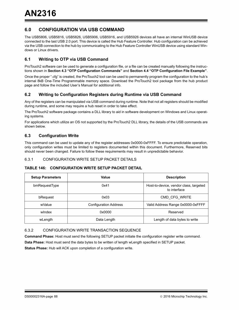
AN2316
6.0 CONFIGURATION VIA USB COMMAND
The USB5806, USB5816, USB5826, USB5906, USB5916, and USB5926 devices all have an internal WinUSB device connected to the last USB 2.0 port. This device is called the Hub Feature Controller. Hub configuration can be achieved via the USB connection to the hub by communicating to the Hub Feature Controller WinUSB device using standard Win-dows or Linux drivers.
6.1 Writing to OTP via USB Command
ProTouch2 software can be used to generate a configuration file, or a file can be created manually following the instruc-tions shown in Section 4.3 “OTP Configuration Commands” and Section 4.4 “OTP Configuration File Example”.
Once the proper “.cfg” is created, the ProTouch2 tool can be used to permanently program the configuration to the hub’s internal 8kB One-Time Programmable memory space. Download the ProTouch2 tool package from the hub product page and follow the included User’s Manual for additional info.
6.2 Writing to Configuration Registers during Runtime via USB Command
Any of the registers can be manipulated via USB command during runtime. Note that not all registers should be modified during runtime, and some may require a hub reset in order to take effect.
The ProTouch2 software package contains a DLL library to aid in software development on Windows and Linux operat-ing systems.
For applications which utilize an OS not supported by the ProTouch2 DLL library, the details of the USB commands are shown below.
6.3 Configuration Write
This command can be used to update any of the register addresses 0x0000-0xFFFF. To ensure predictable operation, only configuration writes must be limited to registers documented within this document. Furthermore, Reserved bits should never been changed. Failure to follow these requirements may result in unpredictable behavior.
6.3.1 CONFIGURATION WRITE SETUP PACKET DETAILS
TABLE 146: CONFIGURATION WRITE SETUP PACKET DETAIL
Setup Parameters Value Description
bmRequestType 0x41 Host-to-device, vendor class, targeted to interface
bRequest 0x03 CMD_CFG_WRITE
wValue Configuration Address Valid Address Range 0x0000-0xFFFF
wIndex 0x0000 Reserved
wLength Data Length Length of data bytes to write
6.3.2 CONFIGURATION WRITE TRANSACTION SEQUENCE
Command Phase: Host must send the following SETUP packet initiate the configuration register write command.
Data Phase: Host must send the data bytes to be written of length wLength specified in SETUP packet.
Status Phase: Hub will ACK upon completion of a configuration write.
DS00002316A-page 88 2016 Microchip Technology Inc.

AN2316
6.4 Configuration Read
This command can be used to read any of the register addresses 0x0000-0xFFFF.
6.4.1 CONFIGURATION READ SETUP PACKET DETAILS
TABLE 147: CONFIGURATION READ SETUP PACKET DETAIL
Setup Parameters Value Description
bmRequestType 0xC1 Device-to-host, vendor class, targeted to interface
bRequest 0x04 CMD_CFG_READ
wValue Configuration Address Valid Address Range 0x0000-0xFFFF
wIndex 0x0000 Reserved
wLength Data Length Length of data bytes to read
6.4.2 CONFIGURATION READ TRANSACTION SEQUENCE
Command Phase: Host must send the following SETUP packet initiate the configuration register read command.
Data Phase: Hub will send the data bytes of length wLength from the address specified in the SETPUP packet.
6.5 Configuration Write Example
1. Command Phase (SETUP Transaction): Send the following SETUP Register Write Command to Endpoint 0 of the USB58xx/USB59xx Hub Feature Controller to write the contents of registers 0x833 which contain the direc-tion control settings for GPIOs 1-7. In this example, GPIOs 4 & 5 will be set as outputs, all other GPIOS will remain at the default input state.
TABLE 148: REGISTER WRITE SETUP COMMAND EXAMPLE
Setup Parameter Value Note
bmRequestType 0x41 —
bRequest 0x03 —
wValue 0x0833 First register in a series of consecutive registers to write from.
wIndex 0x0000 —
wLength 0x0001 1 register is to be read.
FIGURE 5: REGISTER WRITE SETUP TRANSACTION EXAMPLE
2016 Microchip Technology Inc. DS00002316A-page 89

AN2316
2. Data Phase (OUT Transaction): Host sends the one data bytes to set 0x833 = 0x30 after sending the OUT packet.
FIGURE 6: REGISTER WRITE OUT TRANSACTION EXAMPLE
3. Status Phase (OUT Transaction): Host sends an IN packet to complete the USB Transfer. Hub Feature Con-troller responds with a zero length data packet.
FIGURE 7: REGISTER WRITE IN TRANSACTION EXAMPLE
6.6 Configuration Read Example
1. Command Phase (SETUP Transaction): Send the following SETUP Register Read Command to Endpoint 0 of the USB58xx/USB59xx Hub Feature Controller to read the contents of registers 0x833 which contain the direction control settings for GPIOs 1-7.
TABLE 149: REGISTER READ SETUP COMMAND EXAMPLE
Setup Parameter Value Note
bmRequestType 0xC1 —
bRequest 0x04 —
wValue 0x0833 First register in a series of consecutive registers to read from.
wIndex 0x0000 —
wLength 0x0001 4 consecutive registers are to be read.
DS00002316A-page 90 2016 Microchip Technology Inc.

AN2316
FIGURE 8: REGISTER READ SETUP TRANSACTION EXAMPLE
2. Data Phase (IN Transaction): Hub Feature Controller sends the data bytes of length wLength starting from the specified address after receiving an IN packet.
FIGURE 9: REGISTER READ IN TRANSACTION EXAMPLE
3. Status Phase (OUT Transaction): Host sends an OUT packet to complete the USB Transfer. Hub Feature Con-troller responds with a zero length data packet.
FIGURE 10: REGISTER READ OUT TRANSACTION EXAMPLE
2016 Microchip Technology Inc. DS00002316A-page 91

AN2316
APPENDIX A: APPLICATION NOTE REVISION HISTORY
TABLE A-1: REVISION HISTORY
Revision Level & Date Section/Figure/Entry Correction
DS00002316A (12-07-16) Initial release.
DS00002316A-page 92 2016 Microchip Technology Inc.

AN2316
NOTES:
2016 Microchip Technology Inc. DS00002316A-page 93

ANXXXX
DS00002316A-page 94 2016 Microchip Technology Inc.
THE MICROCHIP WEB SITE
Microchip provides online support via our WWW site at www.microchip.com. This web site is used as a means to make files and information easily available to customers. Accessible by using your favorite Internet browser, the web site contains the following information:
• Product Support – Data sheets and errata, application notes and sample programs, design resources, user’s guides and hardware support documents, latest software releases and archived software
• General Technical Support – Frequently Asked Questions (FAQ), technical support requests, online discussion groups, Microchip consultant program member listing
• Business of Microchip – Product selector and ordering guides, latest Microchip press releases, listing of seminars and events, listings of Microchip sales offices, distributors and factory representatives
CUSTOMER CHANGE NOTIFICATION SERVICE
Microchip’s customer notification service helps keep customers current on Microchip products. Subscribers will receive e-mail notification whenever there are changes, updates, revisions or errata related to a specified product family or development tool of interest.
To register, access the Microchip web site at www.microchip.com. Under “Support”, click on “Customer Change Notifi-cation” and follow the registration instructions.
CUSTOMER SUPPORT
Users of Microchip products can receive assistance through several channels:
• Distributor or Representative
• Local Sales Office
• Field Application Engineer (FAE)
• Technical Support
Customers should contact their distributor, representative or Field Application Engineer (FAE) for support. Local sales offices are also available to help customers. A listing of sales offices and locations is included in the back of this document.
Technical support is available through the web site at: http://microchip.com/support

2016 Microchip Technology Inc. DS00002316A-page 95
ANXXXX
Information contained in this publication regarding device applications and the like is provided only for your convenience and may be superseded by updates. It is your responsibility to ensure that your application meets with your specifications. MICROCHIP MAKES NO REPRESENTATIONS OR WARRANTIES OF ANY KIND WHETHER EXPRESS OR IMPLIED, WRITTEN OR ORAL, STATUTORY OR OTHERWISE, RELATED TO THE INFORMATION, INCLUDING BUT NOT LIMITED TO ITS CONDITION, QUALITY, PERFORMANCE, MERCHANTABILITY OR FITNESS FOR PURPOSE. Microchip disclaims all liability arising from this information and its use. Use of Micro-chip devices in life support and/or safety applications is entirely at the buyer’s risk, and the buyer agrees to defend, indemnify and hold harmless Microchip from any and all damages, claims, suits, or expenses resulting from such use. No licenses are conveyed, implicitly or otherwise, under any Microchip intellectual property rights unless otherwise stated.
Trademarks
The Microchip name and logo, the Microchip logo, AnyRate, AVR, AVR logo, AVR Freaks, BeaconThings, BitCloud, CryptoMemory, CryptoRF, dsPIC, FlashFlex, flexPWR, Heldo, JukeBlox, KEELOQ, KEELOQ logo, Kleer, LANCheck, LINK MD, maXStylus, maXTouch, MediaLB, megaAVR, MOST, MOST logo, MPLAB, OptoLyzer, PIC, picoPower, PICSTART, PIC32 logo, Prochip Designer, QTouch, RightTouch, SAM-BA, SpyNIC, SST, SST Logo, SuperFlash, tinyAVR, UNI/O, and XMEGA are registered trademarks of Microchip Technology Incorporated in the U.S.A. and other countries.
ClockWorks, The Embedded Control Solutions Company, EtherSynch, Hyper Speed Control, HyperLight Load, IntelliMOS, mTouch, Precision Edge, and Quiet-Wire are registered trademarks of Microchip Technology Incorporated in the U.S.A.
Adjacent Key Suppression, AKS, Analog-for-the-Digital Age, Any Capacitor, AnyIn, AnyOut, BodyCom, chipKIT, chipKIT logo, CodeGuard, CryptoAuthentication, CryptoCompanion, CryptoController, dsPICDEM, dsPICDEM.net, Dynamic Average Matching, DAM, ECAN, EtherGREEN, In-Circuit Serial Programming, ICSP, Inter-Chip Connectivity, JitterBlocker, KleerNet, KleerNet logo, Mindi, MiWi, motorBench, MPASM, MPF, MPLAB Certified logo, MPLIB, MPLINK, MultiTRAK, NetDetach, Omniscient Code Generation, PICDEM, PICDEM.net, PICkit, PICtail, PureSilicon, QMatrix, RightTouch logo, REAL ICE, Ripple Blocker, SAM-ICE, Serial Quad I/O, SMART-I.S., SQI, SuperSwitcher, SuperSwitcher II, Total Endurance, TSHARC, USBCheck, VariSense, ViewSpan, WiperLock, Wireless DNA, and ZENA are trademarks of Microchip Technology Incorporated in the U.S.A. and other countries.
SQTP is a service mark of Microchip Technology Incorporated in the U.S.A.
Silicon Storage Technology is a registered trademark of Microchip Technology Inc. in other countries.
GestIC is a registered trademark of Microchip Technology Germany II GmbH & Co. KG, a subsidiary of Microchip Technology Inc., in other countries.
All other trademarks mentioned herein are property of their respective companies.
© 2016, Microchip Technology Incorporated, All Rights Reserved.
ISBN: 978-1-5224-1172-7
Note the following details of the code protection feature on Microchip devices:
• Microchip products meet the specification contained in their particular Microchip Data Sheet.
• Microchip believes that its family of products is one of the most secure families of its kind on the market today, when used in the intended manner and under normal conditions.
• There are dishonest and possibly illegal methods used to breach the code protection feature. All of these methods, to our knowledge, require using the Microchip products in a manner outside the operating specifications contained in Microchip’s Data Sheets. Most likely, the person doing so is engaged in theft of intellectual property.
• Microchip is willing to work with the customer who is concerned about the integrity of their code.
• Neither Microchip nor any other semiconductor manufacturer can guarantee the security of their code. Code protection does not mean that we are guaranteeing the product as “unbreakable.”
Code protection is constantly evolving. We at Microchip are committed to continuously improving the code protection features of our products. Attempts to break Microchip’s code protection feature may be a violation of the Digital Millennium Copyright Act. If such acts allow unauthorized access to your software or other copyrighted work, you may have a right to sue for relief under that Act.
Microchip received ISO/TS-16949:2009 certification for its worldwide headquarters, design and wafer fabrication facilities in Chandler and Tempe, Arizona; Gresham, Oregon and design centers in California and India. The Company’s quality system processes and procedures are for its PIC® MCUs and dsPIC® DSCs, KEELOQ® code hopping devices, Serial EEPROMs, microperipherals, nonvolatile memory and analog products. In addition, Microchip’s quality system for the design and manufacture of development systems is ISO 9001:2000 certified.
QUALITYMANAGEMENTSYSTEMCERTIFIEDBYDNV
== ISO/TS16949==

DS00002316A-page 96 2016 Microchip Technology Inc.
AMERICASCorporate Office2355 West Chandler Blvd.Chandler, AZ 85224-6199Tel: 480-792-7200 Fax: 480-792-7277Technical Support: http://www.microchip.com/supportWeb Address: www.microchip.com
AtlantaDuluth, GA Tel: 678-957-9614 Fax: 678-957-1455
Austin, TXTel: 512-257-3370
BostonWestborough, MA Tel: 774-760-0087 Fax: 774-760-0088
ChicagoItasca, IL Tel: 630-285-0071 Fax: 630-285-0075
DallasAddison, TX Tel: 972-818-7423 Fax: 972-818-2924
DetroitNovi, MI Tel: 248-848-4000
Houston, TX Tel: 281-894-5983
IndianapolisNoblesville, IN Tel: 317-773-8323Fax: 317-773-5453Tel: 317-536-2380
Los AngelesMission Viejo, CA Tel: 949-462-9523Fax: 949-462-9608Tel: 951-273-7800
Raleigh, NC Tel: 919-844-7510
New York, NY Tel: 631-435-6000
San Jose, CA Tel: 408-735-9110Tel: 408-436-4270
Canada - TorontoTel: 905-695-1980 Fax: 905-695-2078
ASIA/PACIFICAsia Pacific OfficeSuites 3707-14, 37th FloorTower 6, The GatewayHarbour City, Kowloon
Hong KongTel: 852-2943-5100Fax: 852-2401-3431
Australia - SydneyTel: 61-2-9868-6733Fax: 61-2-9868-6755
China - BeijingTel: 86-10-8569-7000 Fax: 86-10-8528-2104
China - ChengduTel: 86-28-8665-5511Fax: 86-28-8665-7889
China - ChongqingTel: 86-23-8980-9588Fax: 86-23-8980-9500
China - DongguanTel: 86-769-8702-9880
China - GuangzhouTel: 86-20-8755-8029
China - HangzhouTel: 86-571-8792-8115 Fax: 86-571-8792-8116
China - Hong Kong SARTel: 852-2943-5100 Fax: 852-2401-3431
China - NanjingTel: 86-25-8473-2460Fax: 86-25-8473-2470
China - QingdaoTel: 86-532-8502-7355Fax: 86-532-8502-7205
China - ShanghaiTel: 86-21-3326-8000 Fax: 86-21-3326-8021
China - ShenyangTel: 86-24-2334-2829Fax: 86-24-2334-2393
China - ShenzhenTel: 86-755-8864-2200 Fax: 86-755-8203-1760
China - WuhanTel: 86-27-5980-5300Fax: 86-27-5980-5118
China - XianTel: 86-29-8833-7252Fax: 86-29-8833-7256
ASIA/PACIFICChina - XiamenTel: 86-592-2388138 Fax: 86-592-2388130
China - ZhuhaiTel: 86-756-3210040 Fax: 86-756-3210049
India - BangaloreTel: 91-80-3090-4444 Fax: 91-80-3090-4123
India - New DelhiTel: 91-11-4160-8631Fax: 91-11-4160-8632
India - PuneTel: 91-20-3019-1500
Japan - OsakaTel: 81-6-6152-7160 Fax: 81-6-6152-9310
Japan - TokyoTel: 81-3-6880- 3770 Fax: 81-3-6880-3771
Korea - DaeguTel: 82-53-744-4301Fax: 82-53-744-4302
Korea - SeoulTel: 82-2-554-7200Fax: 82-2-558-5932 or 82-2-558-5934
Malaysia - Kuala LumpurTel: 60-3-6201-9857Fax: 60-3-6201-9859
Malaysia - PenangTel: 60-4-227-8870Fax: 60-4-227-4068
Philippines - ManilaTel: 63-2-634-9065Fax: 63-2-634-9069
SingaporeTel: 65-6334-8870Fax: 65-6334-8850
Taiwan - Hsin ChuTel: 886-3-5778-366Fax: 886-3-5770-955
Taiwan - KaohsiungTel: 886-7-213-7830
Taiwan - TaipeiTel: 886-2-2508-8600 Fax: 886-2-2508-0102
Thailand - BangkokTel: 66-2-694-1351Fax: 66-2-694-1350
EUROPEAustria - WelsTel: 43-7242-2244-39Fax: 43-7242-2244-393
Denmark - CopenhagenTel: 45-4450-2828 Fax: 45-4485-2829
Finland - EspooTel: 358-9-4520-820
France - ParisTel: 33-1-69-53-63-20 Fax: 33-1-69-30-90-79
France - Saint CloudTel: 33-1-30-60-70-00
Germany - GarchingTel: 49-8931-9700Germany - HaanTel: 49-2129-3766400
Germany - HeilbronnTel: 49-7131-67-3636
Germany - KarlsruheTel: 49-721-625370
Germany - MunichTel: 49-89-627-144-0 Fax: 49-89-627-144-44
Germany - RosenheimTel: 49-8031-354-560
Israel - Ra’anana Tel: 972-9-744-7705
Italy - Milan Tel: 39-0331-742611 Fax: 39-0331-466781
Italy - PadovaTel: 39-049-7625286
Netherlands - DrunenTel: 31-416-690399 Fax: 31-416-690340
Norway - TrondheimTel: 47-7289-7561
Poland - WarsawTel: 48-22-3325737
Romania - BucharestTel: 40-21-407-87-50
Spain - MadridTel: 34-91-708-08-90Fax: 34-91-708-08-91
Sweden - GothenbergTel: 46-31-704-60-40
Sweden - StockholmTel: 46-8-5090-4654
UK - WokinghamTel: 44-118-921-5800Fax: 44-118-921-5820
Worldwide Sales and Service
11/07/16


![SAMA5D3 Layout Recommendations - Microchip Technologyww1.microchip.com/downloads/en/AppNotes/Atmel... · SAMA5D3 Layout Recommendations [APPLICATION NOTE] 3 Atmel-11284B-ATARM-SAMA5D3](https://static.fdocuments.net/doc/165x107/5ec95b888c0173649011ce25/sama5d3-layout-recommendations-microchip-sama5d3-layout-recommendations-application.jpg)