AN10961 Dimmable CFL using the UBA2027X family
57
AN10961 Dimmable CFL using the UBA2027X family Rev. 2 — 8 June 2012 Application note Document information Info Content Keywords CFL, Triac dimmable, UBA2027X Abstract This application note describes the design of a dimmable Compact Fluorescent Lamp (CFL) with low dimming level using the UBA2027X.
Transcript of AN10961 Dimmable CFL using the UBA2027X family
AN10961Dimmable CFL using the UBA2027X familyRev. 2 — 8 June 2012 Application note
Document information
Info Content
Keywords CFL, Triac dimmable, UBA2027X
Abstract This application note describes the design of a dimmable Compact Fluorescent Lamp (CFL) with low dimming level using the UBA2027X.

NXP Semiconductors AN10961Dimmable CFL using the UBA2027X family
Revision history
Rev Date Description
v.2 20120608 second, updated issue
Modifications: • Text and drawings updated throughout the document.
v.1 20110815 first issue
AN10961 All information provided in this document is subject to legal disclaimers. © NXP B.V. 2012. All rights reserved.
Application note Rev. 2 — 8 June 2012 2 of 57
Contact informationFor more information, please visit: http://www.nxp.com
For sales office addresses, please send an email to: [email protected]

NXP Semiconductors AN10961Dimmable CFL using the UBA2027X family
1. Introduction
This application note describes the design of a dimmable CFL with a low dimming level using the UBA20270 or UBA20271/UBA20272 ICs. The example illustrated is a 20 W application using the UBA20270 with SPS04N60C3 external MOSFETs. At power levels below 20 W, the UBA20271/2 with integrated MOSFETs can be used.
The UBA20270 controller can be used with both the 120 V and 230 V mains voltage applications. Select the UBA20272 for 230 V mains applications and the UBA20271 for 120 V mains applications for optimal performance.
Remark: Unless otherwise stated all voltages are AC.
A standard commercially available phase-cut wall dimmer is used as the triac wall dimmer. This type of dimmer is representative of most dimmers for 120 V or 230 V input mains applications. Some component values in the application need adapting for dimming compatibility when using other dimmers.
The topology is based on a Voltage Source Charge Pump (VSCP) that is intended to create the necessary hold current for the triac in the dimmer. An End of Life (EOL) circuit has been added externally to the main board for evaluation. The circuit senses high lamp voltage and can shut down the IC in the burn state. The coil saturation protection in the IC does not monitor any ignition or high ignition voltage.
2. Scope
This application note is organized as follows:
• Section 3 describes the basic operation of triac dimming
• Section 4 describes application design
• Section 5 Appendix 1: power calculation equations
• Section 7 Appendix 3: inductive mode preheat calculations
AN10961 All information provided in this document is subject to legal disclaimers. © NXP B.V. 2012. All rights reserved.
Application note Rev. 2 — 8 June 2012 3 of 57
NXP Semiconductors AN10961Dimmable CFL using the UBA2027X family
3. Triac dimming
3.1 Triac dimmer circuit
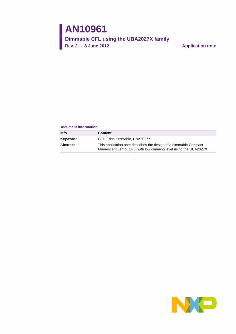
Figure 1 shows the circuit diagram of a triac wall dimmer used in 120 V (RMS) applications.
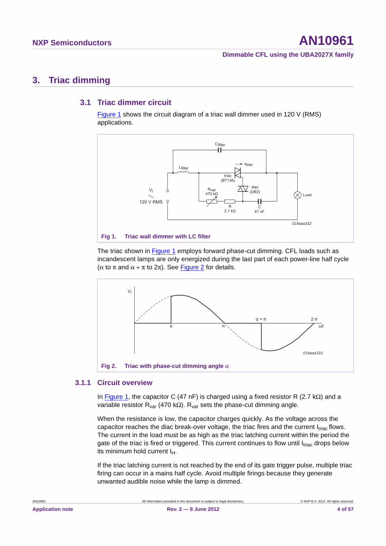
The triac shown in Figure 1 employs forward phase-cut dimming. CFL loads such as incandescent lamps are only energized during the last part of each power-line half cycle (α to π and α + π to 2π). See Figure 2 for details.
3.1.1 Circuit overview
In Figure 1, the capacitor C (47 nF) is charged using a fixed resistor R (2.7 kΩ) and a variable resistor Rvar (470 kΩ). Rvar sets the phase-cut dimming angle.
When the resistance is low, the capacitor charges quickly. As the voltage across the capacitor reaches the diac break-over voltage, the triac fires and the current Itriac flows. The current in the load must be as high as the triac latching current within the period the gate of the triac is fired or triggered. This current continues to flow until Itriac drops below its minimum hold current IH.
If the triac latching current is not reached by the end of its gate trigger pulse, multiple triac firing can occur in a mains half cycle. Avoid multiple firings because they generate unwanted audible noise while the lamp is dimmed.
Fig 1. Triac wall dimmer with LC filter
Fig 2. Triac with phase-cut dimming angle α
019aaa332
Itriac
LoadRvar
470 kΩ
R2.7 kΩ
C47 nF
Cfilter
Lfilter
triac(BT136)
diac(DB3)
120 V RMS
Vi
019aaa333
Vi
α �2 �
ωtα + �
AN10961 All information provided in this document is subject to legal disclaimers. © NXP B.V. 2012. All rights reserved.
Application note Rev. 2 — 8 June 2012 4 of 57

NXP Semiconductors AN10961Dimmable CFL using the UBA2027X family
When the load is an incandescent lamp (resistive load), there is no phase shift between lamp voltage and lamp current. The current can rise high enough within the trigger period of the triac. However, for CFLs, it is not true because of the capacitor in the input filter and the buffer capacitor. The triac is a bidirectional device which operates in two quadrants (see Figure 3). During the negative half cycle, the same process as described earlier is repeated.
In the triac application, the Lfilter and Cfilter can produce ringing of the triac current when the triac latches after a step response. The LC filter in CFL applications incorporates Lfilter and Cfilter. The triac ringing current must remain above IH ensuring the triac remains powered up.
3.2 Triac wall dimmer with VSCS charge pump and CFL ballast
Figure 4 shows a triac wall dimmer and CFL ballast with a Voltage Source Current Source (VSCS) charge pump. The half-bridge MOSFETs in the circuit switch the resonant tank circuit. The lamp current at minimum dimming and lamp voltage at maximum dimming generate the triac hold current ensuring dimming stability.
Fig 3. Typical triac voltage and current characteristics
019aaa334
rated current IL
minimum holdingcurrent IH
breakovervoltage
gate trigger voltage
+I
-I
-V +V
AN10961 All information provided in this document is subject to legal disclaimers. © NXP B.V. 2012. All rights reserved.
Application note Rev. 2 — 8 June 2012 5 of 57

xxxxxxxxxxxxxxxxxxxxx xxxxxxxxxxxxxxxxxxxxxxxxxx xxxxxxx x x x xxxxxxxxxxxxxxxxxxxxxxxxxxxxxx xxxxxxxxxxxxxxxxxxx xx xx xxxxx xxxxxxxxxxxxxxxxxxxxxxxxxxx xxxxxxxxxxxxxxxxxxx xxxxxx xxxxxxxxxxxxxxxxxxxxxxxxxxxxxxxxxxx xxxxxxxxxxxx x x xxxxxxxxxxxxxxxxxxxxx xxxxxxxxxxxxxxxxxxxxxxxxxxxxxx xxxxx xxxxxxxxxxxxxxxxxxxxxxxxxxxxxxxxxxxxxxxxxxxxxxxxxx xxxxxxxx xxxxxxxxxxxxxxxxxxxxxxxxx xxxxxxxxxxxxxxxxxxxx xxx
AN
10961
Ap
plic
ation
no
te
NX
P S
emico
nd
ucto
rsA
N10961
Dim
mab
le CF
L u
sing
the U
BA
2027X fam
ily
���������
���������
���� �!"#$
���%�������������
&'
&'
�&'
���
�#"8� �9"#
�9"#
��#�9:
����������
�;�
All inform
ation provided in this docum
ent is subject to legal disclaim
ers.©
NX
P B
.V. 20
12. All rights reserved
.
Rev. 2 —
8 Jun
e 2012 6
of 5
7
Fig 4. Triac wall dimmer with VSCS charge pump and CFL ballast
����
���
���
�
���������� ����
�
�
#�
���
������� �� �*
�������,*�
/,�
,*� �5���,��
���/��
�,�
���
�����/���������,��/��%��%
���������������,��/��%��%
�%
���
�������� ���������
*���/����������
������������
8" !����$�����$
�9

NXP Semiconductors AN10961Dimmable CFL using the UBA2027X family
The VSCS charge pump maintains triac conduction even at deep dimming since IH is exceeded for low phase-cut angles (down to A = 130°). A minimum hold current of 30 mA to 50 mA is sufficient for most triac dimmers. With a triac phase angle (A), the input voltage, boost and average boost current is shown in Figure 5.
The average input current of the VSCS charge pump follows the input mains voltage.
The dimming control signal for pin DCI is derived from the average of the mains rectified signal. This control signal decreases during dimming and simultaneously the frequency regulation loop of the IC increases the frequency of the half-bridge. These actions ensure the voltages on pins CSI and DCI are equal at 0.34 V as shown in Section 4.6.
(1) Vi
(2) Ibst
(3) Ibst(av)
Fig 5. Input waveforms as function of phase cut angle α
019aaa336
Vi
Vp
0 α � 2 �
Θ = ωt
α + �
tper
(1)
(2)
(3)
(1)
(2)
(3)
AN10961 All information provided in this document is subject to legal disclaimers. © NXP B.V. 2012. All rights reserved.
Application note Rev. 2 — 8 June 2012 7 of 57

NXP Semiconductors AN10961Dimmable CFL using the UBA2027X family
4. Application design
4.1 Simplified circuit diagram
Figure 6 shows the simplified circuit diagram of the UBA20270 controller in a 230 V application including VSCS charge pump.
Fig 6. Simplified circuit diagram of a high PF dimming CFL and UBA20270 controller
���������
�� � ���
���
���
���
�� �
������
��
�� �
���
��
��
��
��
��
������
�������
���� ���
���
� �
�����
�!"���#���$����$�%$&
�%"��'$��'�
����
���$�� ���$��
�'((
�)�'�*
�)#�
��!
��!"�
������+
��+��)
���
��
����
��������
����������
���
���
AN10961 All information provided in this document is subject to legal disclaimers. © NXP B.V. 2012. All rights reserved.
Application note Rev. 2 — 8 June 2012 8 of 57

NXP Semiconductors AN10961Dimmable CFL using the UBA2027X family
4.2 Resonant tank parameters
The resonant inductor (Lres) is the dominating component for the power delivered to the lamp (Plamp). However, the resonant capacitor (Cres) also has influence. Calculate the Lres value to deliver the required lamp current during the boost period. The lamp current during boost is 1.5 times the nominal lamp current. Cres is calculated to ensure that the operating frequency is above 40 kHz in the boost state and the minimum mains voltage is Vmains − 10 %.
The current in the MOSFETs increases for a higher Cres. At a lower Cres, the possibility of hard switching increases because the resonant tank is no longer inductive.
The autotransformer concept lowers the MOSFET current by reducing the voltage on Cres while maintaining the nominal lamp voltage.
An important parameter is the parasitic capacitance inside the transformer Lres and its secondary windings. Parasitic capacitance is especially important for the filament winding connected to the lamp current sense resistor (RCSI). Due to parasitic capacitance, current is directly injected from the resonant tank into RCSI, bypassing the lamp discharge current.
This current degrades deep dimming performance because the lamp discharge current is no longer regulated. The parasitic capacitance must be less than 25 pF to ensure good deep dimming performance.
When the autotransformer winding is used in series with RCSI, the capacitance between Lres and winding T1d must be less than 25 pF. See Section 4.3 for more information.
Table 1 and Table 2 list the resonant tank parameter starting values for 230 V and 120 V mains.
Fig 7. Transformer model Lres with parasitic capacitors Cpar1 and Cpar2
!!!,--�./0
�� ��
����
��)
��!
����
��!�� ��!��
���
���
�!"��%$�#��'������
���$�� ���$��
��!"��#)�
��!� �������
���
���
��� ���
���
AN10961 All information provided in this document is subject to legal disclaimers. © NXP B.V. 2012. All rights reserved.
Application note Rev. 2 — 8 June 2012 9 of 57

NXP Semiconductors AN10961Dimmable CFL using the UBA2027X family
[1] Cres = 5.6 nF.
[2] Cres = 6.8 nF.
[3] Not recommended for resonant topology. Use voltage doubler topology instead.
4.3 Autotransformer
An autotransformer is concept where the primary winding of a transformer is tapped somewhere on the primary winding to generate a lower secondary voltage. Since a transformer works both ways using the center tap as primary, you can also raise the voltage. The disadvantage of the autotransformer is that the primary and secondary are non-isolated. However, when used in a CFL application, this is not a problem.
The autotransformer concept is mainly for the 120 V resonant topology. The concept reduces the reactive half-bridge loading by lowering the voltage on the resonant capacitor. In doing so, overall efficiency improves by 30 %.
Figure 6 shows the autotransformer setup. T1a forms the primary winding and T1d the secondary winding of the autotransformer.
In all applications, the output voltage of the secondary winding of the autotransformer is set at 20 V (RMS). The nominal lamp voltage increases/reduces, depending on how the primary and secondary winding are added in series.
Remark: Take note of the dots in the transformer windings if the voltage is increased/reduced. They determine how the windings are used in the schematics (see Figure 22 to Figure 25).
Use the autotransformer for 120 V mains in two cases and when the nominal lamp voltage is:
• > 110 V: to lower the voltage on the resonant tank
• < 95 V: to increase the voltage on the resonant tank
Table 1. Resonant tank values 230 V mains Applicable to all values: Cres = 3.3 nF, Cblock = 47 nF, CCP = 680 pF, and Cy = 10 nF.
PIN (W) Plamp (W) Vlamp (V) Ilamp (mA) Lres with boost (mH)
Lres without boost (mH)
15 13 105 120 2.5 2.7
18 16 100 160 2 2.5
20 18 110 160 2 2
23 21 110 190 2 2
Table 2. Resonant tank values 120 V mains Applicable to all values: Cblock = 22 nF, CCP = 680 pF, and Cy = 15 nF.
PIN (W) Plamp (W) Vlamp (V) Ilamp (mA) Lres with boost (mH)
Lres without boost (mH)
13 11 100 110 1.2 1.2[1]
15 13 105 120 - 1.2[1]
15 13 105 120 1 -[2]
20 18 110 160 - 1[2][3]
AN10961 All information provided in this document is subject to legal disclaimers. © NXP B.V. 2012. All rights reserved.
Application note Rev. 2 — 8 June 2012 10 of 57

NXP Semiconductors AN10961Dimmable CFL using the UBA2027X family
4.4 Voltage source current source charge pump
Take into account the following four factors to design the charge pump electronic ballast optimally.
• The buffer capacitors voltage rating limits the maximum DC bus voltage
• Satisfying power factor condition: PF ≥ 0.6
• Maintain Zero Voltage Switching (ZVS)
• Input and output power balance
The design guideline for the VSCS-CP electronic ballast with enhanced conduction angle is:
• Set the lowest dim setting or monitor the bus voltage during preheat
• Set input voltage to the nominal line voltage +10 %
• Charge pumped bus voltage value must be Vbus ≤ bus capacitor voltage rating
• At nominal power (no dimming) PF ≥ 0.6
Usually, the bus capacitors voltage rating is the limiting factor in the design and not the voltage rating of the IC. The absolute maximum of the bus voltage is 300 V (DC) for the UBA20271 and 550 V (DC) for the UBA20270 and UBA20272. See the appendix sections for more detailed design equations.
Choose a Voltage Source Currents Source (VSCS) charge pump (see Figure 4) over the more traditional single voltage source charge pump ballast because:
• lower bus voltage stress at light load
• lower values for Cres and so lower reactive losses good hold current for triac dimmers
• low lamp voltage dependency
• lower lamp crest factor
The effect of both charge pumps is inconsistent. The voltage source charge pump helps at the deeper dim levels where the lamp voltage becomes more dominant. It assists in maintaining the large conduction angle for phase cut dimmers. As the lamp crest factor is close to 1.7 which ensures better lamp life.
In addition, the mains harmonic distortion is lower and the power factor under nominal conditions is much better. The only disadvantage is the current transformer that is required to measure the lamp voltage. Section 8 shows an alternative circuit that solves the problem. The current source pump is driven form an additional winding on the resonant inductor.
Table 3. Transformer ratios for 230 V and 120 V mains
Lres with boost (mH)
T1d ratio (Lres: T1d) Lres without boost (mH)
T1d ratio (Lres: T1d)
Transformer ratio 230 V
2 9.74:1 2.5 9.44:1
2.5 9.44:1 2.7 10.27:1
Transformer ratio 120 V
1 7.26:1 1.2 6.84:1
AN10961 All information provided in this document is subject to legal disclaimers. © NXP B.V. 2012. All rights reserved.
Application note Rev. 2 — 8 June 2012 11 of 57
NXP Semiconductors AN10961Dimmable CFL using the UBA2027X family
At nominal lamp power, the average input current the charge pump delivers, the input current and the input power are calculated in Equation 1 and Equation 2:
Average input current:
(1)
Input power:
(2)
Where:
• Vi(pk) = peak input voltage
• fs(hb) = the half-bridge switching cycle
• Vbus = bus voltage (see Figure 5)
See Ref. 3 for more information.
There is no unity power factor condition for the VSCS charge pump with enlarged conduction angle. The second term in Equation 1 is always > 0, because the current source charge pump is dominant over the voltage source charge pump.
The power delivered to the lamp is:
(3)
Where:
• ωs = 2π ⋅ fs• Vlamp = lamp RMS voltage
• Lres = resonant indicator
• Cres = resonant capacitor plus the equivalent resonant capacitor (see Section 5)
• C = inductive mode heating circuit secondary capacitance which is transferred to the primary side.
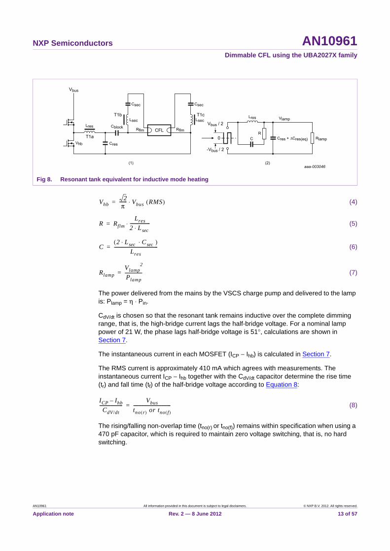
The expression for Plamp in Equation 3 has been derived using the equivalent circuit shown in Figure 8.
Ii av( ) fs hb( ) Cy2 Vi fs hb( ) Cy2
ILres
Cy2 fs hb( ) π⋅ ⋅--------------------------------- Vbus–⋅ ⋅+⋅ ⋅=
Pi12--- fs hb( ) Cy2 Vi pk( )
2 2π--- fs hb( ) Cy2 Vi pk( )
Ires
Cy2 fs hb( ) π⋅ ⋅--------------------------------- Vbus–⋅ ⋅ ⋅ ⋅+⋅ ⋅ ⋅=
Plamp
Vlamp2
ωs Lres⋅--------------------
2 Vbus⋅π Vlamp⋅----------------------
2
1 ωs2
Lres C⋅ ⋅–( )2
1 ωs2
Lres C Cres+( )⋅ ⋅–( )2
–⋅⋅=
AN10961 All information provided in this document is subject to legal disclaimers. © NXP B.V. 2012. All rights reserved.
Application note Rev. 2 — 8 June 2012 12 of 57
NXP Semiconductors AN10961Dimmable CFL using the UBA2027X family
(4)
(5)
(6)
(7)
The power delivered from the mains by the VSCS charge pump and delivered to the lamp is: Plamp = η ⋅ Pin.
CdV/dt is chosen so that the resonant tank remains inductive over the complete dimming range, that is, the high-bridge current lags the half-bridge voltage. For a nominal lamp power of 21 W, the phase lags half-bridge voltage is 51°, calculations are shown in Section 7.
The instantaneous current in each MOSFET (ICP − Ihb) is calculated in Section 7.
The RMS current is approximately 410 mA which agrees with measurements. The instantaneous current ICP − Ihb together with the CdV/dt capacitor determine the rise time (tr) and fall time (tf) of the half-bridge voltage according to Equation 8:
(8)
The rising/falling non-overlap time (tno(r) or tno(f)) remains within specification when using a 470 pF capacitor, which is required to maintain zero voltage switching, that is, no hard switching.
Fig 8. Resonant tank equivalent for inductive mode heating
���
�����)�'�* �(�" �(�"
����
�����1� ����2�34 ��!"�
��!"�
����
��
����
����
�)#�
����
�+)
2�4 2�4���������
-
,�)#�����
�)#�����
����
��) ���
��!
Vhb2
π------- Vbus RMS( )⋅=
R Rflm
Lres
2 L sec⋅------------------⋅=
C2 L sec C sec⋅ ⋅( )
Lres----------------------------------------=
Rlamp
Vlamp2
Plamp----------------=
ICP Ihb–CdV/dt
---------------------Vbus
tno r( ) or tno f( )----------------------------------=
AN10961 All information provided in this document is subject to legal disclaimers. © NXP B.V. 2012. All rights reserved.
Application note Rev. 2 — 8 June 2012 13 of 57

NXP Semiconductors AN10961Dimmable CFL using the UBA2027X family
4.5 Inductive mode preheating and Sum of Squares (SoS)
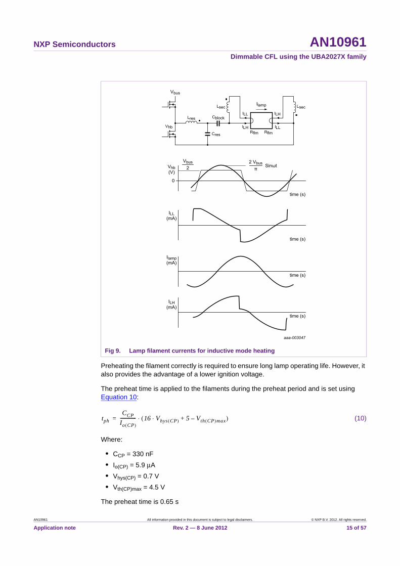
The lifetime of the electrode determines the lifetime of a fluorescent lamp. Keep the electrode temperature within certain limits to ensure sufficient lifetime. Above a certain temperature, the electrodes are too hot, leading to enhanced evaporation of the emissive material and severe end-blackening. Below a certain temperature the electrode is too cold and sputtering of the emitter occurs, leading to an extremely short life of the lamp.
The Sum of Squares (SoS) is a measure of the expected amount of heat generated in the filaments and is expressed as:
(9)
Where:
• ILH = Ilamp + ILL
Figure 9 shows the waveform direction of ILL and ILH against time for the period the filaments are inductively preheated. By definition the higher of the two currents is called ILH, the lower of currents ILL. In addition to the relation between the lamp current and the Lead-High current, the Lead-Low current (ILL) can have any value lower than the maximum allowed Lead-Low current. Lead-Low currents exceeding the maximum allowed Lead-Low current cause accelerated end-blackening.
Within limits of the nominal lamp current (Ilamp), additional heating is not strictly required. If the lamp current is dimmed over a broader range, additional heating must be supplied to the electrode for it to maintain its optimum temperature. This is equivalent to the ideal target value of 4.75 times the cold filament resistance. In this case, keep the currents in the lead-in wires within limits. The best lifetime and the minimum end-blackening of the lamp is obtained when the “target setting” for ILH and Ilamp is observed over the entire dimming range.
Keep the SoS value below a maximum value where the filament resistance is 5.5 times (minimum = 4 times) the cold filament resistance. Alternatively, keep the minimum and maximum settings the manufacturer has specified.
However, an SoS setting close to the target setting is preferred for optimal long-life operation of the lamp. Maintaining, within specification, adequate filament preheating and optimum SoS is difficult, because these are conflicting requirements.
Two points of the SOS target line are easiest to obtain:
• Preheat or deep dimming:
The lamp current is significantly lower than the heating current.
• Nominal:
The nominal lamp discharge current dominates the heating current.
The power required to heat the filament to a constant of 4.75 times the cold resistance can easily be obtained by using a low voltage DC power source and measuring the power required from the source to set the condition. The line between these points can be used as the SoS target over the dimming range.
SoS ILL2
ILH2+=
AN10961 All information provided in this document is subject to legal disclaimers. © NXP B.V. 2012. All rights reserved.
Application note Rev. 2 — 8 June 2012 14 of 57
NXP Semiconductors AN10961Dimmable CFL using the UBA2027X family
Preheating the filament correctly is required to ensure long lamp operating life. However, it also provides the advantage of a lower ignition voltage.
The preheat time is applied to the filaments during the preheat period and is set using Equation 10:
(10)
Where:
• CCP = 330 nF
• Io(CP) = 5.9 μA
• Vhys(CP) = 0.7 V
• Vth(CP)max = 4.5 V
The preheat time is 0.65 s
Fig 9. Lamp filament currents for inductive mode heating
����������
����
����
�)#�
�+)
�)�'�*
���� �������
���
���
�(�" �(�"���
�)#�
���2"�4
��!"�2"�4
���2"�4
�+)2�4
����)#� �%$5�
��!"�
-
�%"��2�4
�%"��2�4
�%"��2�4
�%"��2�4
tph
CCP
Io CP( )-------------- 16 Vhys CP( ) 5 Vth CP( )max–+⋅( )⋅=
AN10961 All information provided in this document is subject to legal disclaimers. © NXP B.V. 2012. All rights reserved.
Application note Rev. 2 — 8 June 2012 15 of 57

NXP Semiconductors AN10961Dimmable CFL using the UBA2027X family
The preheat frequency can be set by measuring the voltage across the SLS resistor between the source and ground of the lower MOSFET (see Figure 25). The half-bridge frequency starts at fVCO(max) and sweeps down until the voltage on pin SLS reaches the Vph level that is defined in the specification. The sweep then stops for the duration of the preheat time tph.
During the preheat time, the frequency is controlled so that the voltage on pin SLS stays constant, implying that the half-bridge current is kept constant. The half-bridge current level can be adapted by changing the value of the SLS resistor. However, the value selected must not cause the lamp to ignite during the preheat time. Also, the saturation protection and overcurrent protection use the same resistor. Practical values for RSLS at 120 V mains are between 0.9 Ω and 1.5 Ω. At 230 V mains, they are between 1.5 Ω and 2.2 Ω. A value that is too low causes the lamp voltage to become too high during low mains. A value that is too high causes the triggering of the saturation protection.
Adjust the secondary turns or the secondary capacitors if the preheat energy or SoS is not within limits.
Figure 10 shows the frequency as a function of time.
The relationship for the preheat (filament) current for Inductive mode heating is calculated in Section 7.
When the half-bridge frequency is 71 kHz, the non-overlap time is 1.5 μs and the RMS filament current is 0.25 A. The filament power dissipated is approximately 1.6 W when the hot filament resistance Rfilter = 25 Ω. The power supplied to the filament during preheat is fs × C × Vsec
2 and for a capacitance of 47 nF:
(11)
Fig 10. Frequency as a function of time during start-up
019aaa340tph
t (µs)
f (kHz)
fVCO(max)
fph
fnom
fVCO(max)
VsecVpri
n---------=
AN10961 All information provided in this document is subject to legal disclaimers. © NXP B.V. 2012. All rights reserved.
Application note Rev. 2 — 8 June 2012 16 of 57

NXP Semiconductors AN10961Dimmable CFL using the UBA2027X family
Where:
• Vpri = 350 V
•
The power supplied to the filament is approximately 1.6 W.
The hot-to-cold ratio of the filament resistance must preferably be 4.75:1 to guarantee sufficient filament current is provided at the end of the preheat period. If however, this conflicts with the SoS at deep dimming, choose the lower ratio of 4:1. A higher ratio can overload the filament and reduce the operating lifetime. After the preheat period, the frequency sweeps down rapidly and the lamp ignites when the ignition frequency (fign) is reached. The lamp can be modeled now as a (negative) resistance where:
(12)
Before ignition, the lamp has a much higher impedance as no lamp current is flowing. Both characteristics are shown in Figure 11.
Capacitor CCF, resistor RRREF and the voltage on pin CI determine the internal Voltage Controlled Oscillator (VCO) frequency (half-bridge frequency). The minimum and maximum frequencies are as defined in Equation 13:
(13)
Example:
• Plamp = 20 W
• Vlamp = 110 V
• Lres = 2 mH
• Lsec = 10 μH
• Cres = 4.7 nF
(14)
(15)
(16)
nLres
Lsec--------- 16==
Rlamp
Vlamp2
Plamp----------------=
fVCO min( ) 40.5 103 100 10
12–⋅CCF
-------------------------- 33 10
3⋅RRREF------------------
⋅ ⋅ ⋅=
and
fVCO max( ) 2.5 fmin⋅=
Rlamp
Vlamp2
Plamp---------------- 605 Ω= =
Cp 2 CsecLsecLres--------- 33 10
9– nF⋅=⋅ ⋅=
H ω,Rlamp( )p ω( )2
Lres Cp 1+⋅ ⋅
p ω( )2Cres Cp+( ) Lres p ω( )
Lres
Rlamp------------- 1+⋅+⋅ ⋅
------------------------------------------------------------------------------------------------------------=
AN10961 All information provided in this document is subject to legal disclaimers. © NXP B.V. 2012. All rights reserved.
Application note Rev. 2 — 8 June 2012 17 of 57

NXP Semiconductors AN10961Dimmable CFL using the UBA2027X family
Where:
• Cp = 2.4 pF ⋅ 10−10
• ω(f) = 2 ⋅ π ⋅ f
• p(ω) = j ⋅ ω
4.6 Dimming using frequency feedback control loop
After lamp ignition and when the IC is in the burn state, the internal average current sensor at pin CSI is regulated to the DCI voltage minus an offset. The voltage on pin CSI is derived by sensing the lamp current and converting it to voltage using a sense resistor as shown in Figure 12.
This voltage is supplied to the CSI pin as:
(17)
The high-frequency feed through the transformer and ignition spike is reduced by adding a low-pass filter. After Rsense, the −3 dB point of the filter is set to 1.5 MHz.
Because the UBA2027X incorporates overpower protection, the maximum voltage pin CSI is regulated to in the burn state is 1 V (RMS). This means that the unboosted lamp current is calculated with Equation 18:
(18)
(1) Hω(f, 2000 Ω)
(2) Hω(f, 650 Ω)
Fig 11. Transfer of frequency before and after ignition
f (kHz)0 806020 40
019aaa341
1
2
3
Vlamp / Vhb(V)
0
(1)
(2)
(1)
Vi CSI( ) Ilamp RMS( ) Rsense⋅=
Ilamp RMS( ) 1Rsense---------------=
AN10961 All information provided in this document is subject to legal disclaimers. © NXP B.V. 2012. All rights reserved.
Application note Rev. 2 — 8 June 2012 18 of 57

NXP Semiconductors AN10961Dimmable CFL using the UBA2027X family
The DCI pin voltage is derived from the mains rectified signal (see Figure 13). This circuit is designed to give a dimming voltage range of 1.5 V to 0.25 V for a phase-cut range of α = 0° − 25° to 130°, respectively. This voltage (after being averaged with the double filter C8, C10, R5 and R6) is applied to pin DCI where:
The nominal voltage on pin DCI is set 10 % higher than the maximum of 1.34 V. The extra 10 % compensates for small line voltage variations and the minimum phase cut angle that every phase cut dimmer incorporates. This compensation ensures that the lamp does not dim immediately but remains at a constant output. In this setup, the maximum lamp voltage occurs in the first 0° to 25° of the phase angle. The diac or gate trigger circuit’s leading-edge phase-cut dimmers cannot start from 0° which always presents a small phase cut. The exact DCI can be calculated using:
(19)
Where:
• Vpk = the rectified peak voltage
• Vd = the diode junction voltage drop
(20)
(21)
The circuit that adds a rectified current from the SLS pin to resistor R11 adds a small offset to the DCI when the lamp ignites. Most triac dimmers sense the ignition of the lamp as a load change. They change the triac trigger angle to a smaller phase-cut angle in most cases. Because of this change the DCI voltage drops below 0.24 V for a short moment, when the dimming level is set to a very low level. The lamp turns off. The added rectified
Fig 12. Lamp current sensing
Table 4. Component values
Component 230 V 120 V
R8 470 kΩ 270 kΩ
R9 470 kΩ 270 kΩ
R10 33 kΩ 39 kΩ
R11 39 kΩ 39 kΩ
��������
�+�
�+�
��!"�2��4
�%2���4
���$��
Vpk R10 R5 R11+( ) R10 R8 R9+( ) Vd⋅ ⋅+⋅ ⋅R10 R5 R11+( ) R10 R8 R9+( ) R8 R9+( ) R5 R11+( )⋅ ⋅ ⋅+⋅------------------------------------------------------------------------------------------------------------------------------------------------------- Vd– R11
R5 R11+-----------------------⋅
Vi DCI( )calc=
Vi DCI( )offsetR
R R11+-------------------- Vi SLS( ) Vd–( )⋅=
Vi DCI( ) Vi DCI( )offset Vi DCI( )calc+=
AN10961 All information provided in this document is subject to legal disclaimers. © NXP B.V. 2012. All rights reserved.
Application note Rev. 2 — 8 June 2012 19 of 57

NXP Semiconductors AN10961Dimmable CFL using the UBA2027X family
SLS voltage resolves this problem. It lifts the DCI level for a short moment during the ignition of the lamp, creating a stable and flicker-free lamp ON/lamp OFF at lowest dim level. The voltage drop of the diode also prevents that during preheat the DCI voltage is affected.
The loop regulation is in balance when the RMS voltage of Vi(CSI) equals Vi(DCI) (−0.34 V).
Voltage levels between 1.34 V and 5 V do not increase the maximum regulation voltage of 1 V (RMS) on pin CSI.
During dimming, regulation is achieved with frequency control:
• Vi(DCI) decreases
• The voltage on pin CI decreases
• frequency of the half-bridge increases
• The lamp current decreases
• The RMS value of Vi(CSI) decreases
When the voltage on pin DCI is between 0.24 V and 1.34 V, the loop regulation forces the RMS voltage of Vi(CSI) to follow Vi(DCI) until an equilibrium is reached.
4.7 CI integrator circuit and differential feedback
Normally, a simple resistor (R) in series with a 220 nF integrating capacitor connected to pin CI is used to get a stable lamp operation. The integrating capacitor can be kept constant and the resistor can be tuned to the time constant of the connected burner. Select a resistor value that obtains the most constant and flat lamp current regulation over the entire dimming range.
Fig 13. Dimming control
���������
�%�2��4
��
�%2���4
�%2���4
�6�1��0
��-
�7 �.
�6 ���
��
�)#�
��8 ��-
�%"��'$��'�
AN10961 All information provided in this document is subject to legal disclaimers. © NXP B.V. 2012. All rights reserved.
Application note Rev. 2 — 8 June 2012 20 of 57

NXP Semiconductors AN10961Dimmable CFL using the UBA2027X family
This simple resistor (R) and capacitor (C) series network cannot solve the problem of burners showing significant lamp flicker for the first minute of a cold lamp start-up.
When using high-temperature amalgam lamps flicker can be observed when the lamp is new, is cold or has been switched off for a long time. Once the lamp is warm or aged, the flickering reduces and eventually disappears.
Differential feedback reduces the first run-up lamp flicker to a minimum (see Figure 15).
Typical 230 V: R3 = 1 kΩ; R28 = 3.3 kΩ; C4 = 10 nF
Fig 14. CI networks
Fig 15. Differential feedback circuit in 120 V mains application
����������
��
�9��-�$�
�9�:��*;
��
�9��-�$�
�98:9�*;
��
!4���-�����(!#�� )4��9-�����(!#�� �4�'��%'$
�9��-�$�
�8�(
�9��'<
��6����#��
Rresult Rhigh Rlow–=
Cf1
2π R28 3000⋅ ⋅( )------------------------------------------=
����������
��!
�9/
��8)
�96�--�$�
�9/�--�$�
���*;
���7.-���
�'��%$���
�'��%$���
�'��%$��
�$=��'���������'�
�!"���#���$���$������%��'�
������
��!"�
���>?68����
��)
��8!�@�00��8
.:6�;��67.-�;
�9�7-�;
�@A7.
�96
��0�7-�$�
99-�;
�9.
8/-�;
�.
��B�
�%((���$�%!��(���)!�*
�9��-�$�
AN10961 All information provided in this document is subject to legal disclaimers. © NXP B.V. 2012. All rights reserved.
Application note Rev. 2 — 8 June 2012 21 of 57
NXP Semiconductors AN10961Dimmable CFL using the UBA2027X family
The differential feedback circuit consists of an envelope detector and the differential gain stage. The envelope detector supply comes from a secondary dV/dt supply set up by D2b and C37 to avoid overloading the start-up resistors.
The negative envelope of the lamp current is sensed on the lamp current sense resistor R14. Resistor R38 and capacitor C29 filter it to approximately 4 kHz. Resistors R36 and R28 and capacitor C6 set the amount of differential feedback.
The circuit in Figure 15 is for a 120 V lamp with a particular 12.5 W burner.
Different burners from other manufactures have different lamp specifications. Therefore the lamp time constants differ. The circuit still requires some tuning to get the right amount of differential feedback. Keep capacitor C3 always at 220 nF to tune the circuit. Different values for resistors R3, R28 and R36 can be chosen to get the right mix of integrator action and differential feedback.
In a 230 V lamp the differential feedback is not required as Cres is lower. A simple RC integrator is sufficient (see Figure 14 (b)).
In some cases, flicker can be seen when the lamp is dimmed to about 10 % to 80 %. However, it is stable at 5 % to 10 % dimming. In this case, a larger and smaller resistor R3 is preferred. The larger resistor for the gain at lower frequencies, the smaller resistor for the gain at higher frequencies in the feedback loop. Figure 14 (c) shows the circuit that can be used to resolve the issue.
Temporarily replacing R3 with a variable resistor of 10 kΩ in series with a 330 Ω resistor can assist in finding the high and low values for resistor R3. Adjust R3 by looking at the lamp voltage over dimming on an oscilloscope. The envelope of the lamp voltage over dimming must show a line that is as level as possible. Deep valleys in the envelope show that the chosen value for resistor R3 is too low. Noise with peaks above the envelope at the point where the buffer capacitor is charged from the mains indicates that the chosen value for resistor R3 is too low. The corner frequency of resistor R28 and capacitor C4 is set at around 3 kHz. Up to about 2 kHz there is a higher gain. At 11 kHz, there is a lower gain in the feedback loop.
(22)
(23)
At 230 V (typical): R3 = 1 kΩ, R28 = 3.3 kΩ and C4 = 18 nF
Special tools are available to adjust this circuit to fit the parameters of the lamp.
4.8 Boosting of the lamp
When first switched on (in the first 180 s), Amalgam lamps have a slow run up or less light output. A fixed ratio of 1.5:1 boosts the lamp current to resolve this problem. The capacitor on pin CB (CCB) sets the boost time and is calculated with Equation 24.
(24)
Rresult Rhigh Rlow–=
Cf1
2π R28 3000⋅ ⋅( )------------------------------------------=
tbst
CCB
Io CB( )-------------- 126 Vhys CB( ) Vth CB( )min 0.6–+⋅( )⋅=
AN10961 All information provided in this document is subject to legal disclaimers. © NXP B.V. 2012. All rights reserved.
Application note Rev. 2 — 8 June 2012 22 of 57

NXP Semiconductors AN10961Dimmable CFL using the UBA2027X family
Where:
• Io(CB) = 1 μA
• Vhys(CB) = 2.5 V
• Vth(CB)min = 1.1 V
• CCB = 150 nF
These parameters lead to a boost time of 48 s. Shorting pin CB to ground turns off the boost circuit.
During the boost period, the maximum voltage on pin CSI regulates to 1.5 V (RMS), effectively boosting the lamp current by a factor of 1.5. It is important that during the boost the filament current is still operating within their SoS limits, to avoid degrading the lamp operating life. If the lamp does not have higher current rated filaments (not intended for boost), then:
• Lower the lamp operating current to 80 % of nominal
• Run boost at 1.25 % of nominal
In simple terms, run a 12 W burner at 10 W nominal and 15 W during boost.
With higher rated lamps, set the power use to the full 150 %. For example, use an 18 W burner for a 12 W lamp because the filaments automatically have a higher rating.
4.9 Setting Minimum Dimming Level (MDL)
The minimum dim level can be used to prevent the lamp from entering the glow phase at the lowest setting of the dimmer. Glow is observed when there is some light coming from the lamp but the CFL tube is not fully lit. This effect also causes flicker when the lamp changes from glow to normal burn constantly. Resistor RMDL sets the MDL voltage as
follows: . It is lamp-dependent.
4.10 IC supply and capacitive mode protection
The IC starts when its supply voltage VDD exceeds VDD(start). Rstartup completes the first charge of the supply decoupling capacitor CVDD. This resistor must be large enough to supply at least 0.32 mA at 12.5 V. The half-bridge begins to switch and the IC is supplied using a capacitor that is connected at the half-bridge (see Figure 16).
A larger capacitor is required when more current is required in the external MOSFETs and thus in the internal drivers which drive the external MOSFETs. However if CdV/dt is too large, hard switching at higher frequencies can occur since the non-overlap time decreases at higher frequencies (adaptive non-overlap time). The minimum required value can be calculated using:
(25)
A capacitor value of 470 pF is a good compromise between these two situations. A 12 V Zener diode clamps the voltage and a fast recovery diode supplies it to VDD.
VMDL RMDL IMDL src( )×=
CdV/dt
2 the gate ch earg of the MOSFETsIDD
fbridge min( )--------------------------+⋅
Vbus min( )---------------------------------------------------------------------------------------------------------------------------------------=
AN10961 All information provided in this document is subject to legal disclaimers. © NXP B.V. 2012. All rights reserved.
Application note Rev. 2 — 8 June 2012 23 of 57
NXP Semiconductors AN10961Dimmable CFL using the UBA2027X family
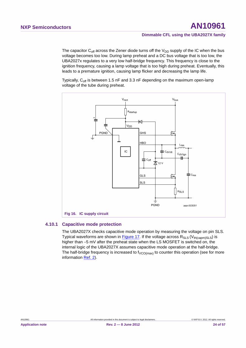
The capacitor Coff across the Zener diode turns off the VDD supply of the IC when the bus voltage becomes too low. During lamp preheat and a DC bus voltage that is too low, the UBA2027x regulates to a very low half-bridge frequency. This frequency is close to the ignition frequency, causing a lamp voltage that is too high during preheat. Eventually, this leads to a premature ignition, causing lamp flicker and decreasing the lamp life.
Typically, Coff is between 1.5 nF and 3.3 nF depending on the maximum open-lamp voltage of the tube during preheat.
4.10.1 Capacitive mode protection
The UBA2027X checks capacitive mode operation by measuring the voltage on pin SLS. Typical waveforms are shown in Figure 17. If the voltage across RSLS (Vth(capm)SLS) is higher than −5 mV after the preheat state when the LS MOSFET is switched on, the internal logic of the UBA2027X assumes capacitive mode operation at the half-bridge. The half-bridge frequency is increased to fVCO(max) to counter this operation (see for more information Ref. 2).
Fig 16. IC supply circuit
�� �
���!��#�
���
���
�)#������
���
���
���
�� �
������
�'((
����
����
����
����
����%&$��
���������
AN10961 All information provided in this document is subject to legal disclaimers. © NXP B.V. 2012. All rights reserved.
Application note Rev. 2 — 8 June 2012 24 of 57

NXP Semiconductors AN10961Dimmable CFL using the UBA2027X family
4.11 Mains input filtering
A Resistance, Inductance, Capacitance (RLC) filter is used to filter the mains to maintain high EMI performance at the half-bridge frequency and across the harmonic range. The inductor blocks the HF charge pump and operating current, the capacitor provides a low ohmic path for this current. HF current damping can be determined using Equation 26.
Because of the diode bridge and the buffer capacitor in the application, the RLC filter does not have a constant load. It can cause mains current ringing when connected to a leading-edge triac dimmer. This ringing in turn causes the triac to shut down after it has been triggered. This leads to unwanted audible noise because of multiple triggering of the triac. Figure 18 shows a solution for suppressing multiple triggering.
Fig 17. Driver, half-bridge and Vi(SLS) capacitive mode detection
019aab031
Vth(capm)SLS0
Vi(SLS)
Vhb
V(GH-SH)
VGL
Fig 18. Multiple fire suppression
����������
�����$�
�8���$�
�)#�1
��
�
��
"!%$�%$�#�
8:/�;��A
��
8:/�"�
�����$�
�����-�;
��� 8--/�
�9� 8--/�
��� 8--/�
�8� 8--/�
�����-�;
��
�--�$�
AN10961 All information provided in this document is subject to legal disclaimers. © NXP B.V. 2012. All rights reserved.
Application note Rev. 2 — 8 June 2012 25 of 57

NXP Semiconductors AN10961Dimmable CFL using the UBA2027X family
Resistors Rd1 and Rd2 and capacitor Cd create a load for the triac dimmer at higher frequencies which effectively dampen the ringing in the mains current. Rd is split in two enabling distribution of the power into small resistors. Optimum damping for a parallel
damped filter is obtained when and .
Given:
• L = 4.7 mH
• C = 22 nF
• R = 4.7 Ω
(26)
The calculated damping at 45 kHz relative to 50 Hz is more than 60 dB (see Figure 19 (a)).
The fused resistor R (= 4.7 Ω ) is used to limit/damp the inrush current during start-up and during large steps of input current during triac operation (see for more information Ref. 1).
a. HF current damping
b. Graphical representation
Fig 19. Transfer function input filter
Rd L2C2-------= Cd 4 C2⋅=
20 1
1 ω2L C⋅ ⋅+( )
2ω R C⋅ ⋅( )2+
--------------------------------------------------------------------------log
Vi mains
R
iHF
L
C
019aab032(1)
019aab033
-60
-20
20
G(2� · f)
-100
f (Hz)102 105104103
AN10961 All information provided in this document is subject to legal disclaimers. © NXP B.V. 2012. All rights reserved.
Application note Rev. 2 — 8 June 2012 26 of 57

NXP Semiconductors AN10961Dimmable CFL using the UBA2027X family
4.12 Extra protections
4.12.1 OverPower Protection (OPP)
Since the measured lamp current is clamped at 1 V (RMS), the lamp current remains nominal during mains voltage fluctuations. During overvoltage conditions, the half-bridge frequency increases to keep the lamp current constant. Maintain a 10 % higher voltage level on the DCI pin than the required maximum of 1.34 V for this reason. This action resolves any AC line voltage changes in underpower situations.
4.12.2 Coil Saturation Protection (CSP) and OverCurrent Protection (OCP)
The resonant tank inductor is one of the largest components in the application. Therefore it is practical to select the smallest inductor possible. The maximum current capability of a coil is only important at power-up. Choose a parameter that is sufficient under CFL cold start conditions. During warm starts coil parameters are different as the core material degrades at higher temperatures. These conditions often lead to saturation of the coil when the CFL lamp is ignited. Saturation in turn leads to excessive dissipation of the half-bridge MOSFETs or even the destruction of the MOSFETs.
The IC is equipped with coil saturation protection. This protection enables the use of small inductors in the resonant tank and the inverter without destroying the power MOSFETs.
The circuit monitors the current through the source of the lower MOSFET. The current forces a voltage across RSLS. If the voltage is greater than 2.5 V (set by R17 in Figure 23 and Figure 25) of the current during ignition, the IC limits the frequency decrease. The IC shuts down, if the lamp does not ignite within a quarter of the preheat time.
Only for the UBA20271 and UBA20272 the coil saturation threshold can be adjusted to lower saturation currents.
Fig 20. Coil saturation
019aab034
Vi(SLS)(V)
coil saturates
coil just saturating
AN10961 All information provided in this document is subject to legal disclaimers. © NXP B.V. 2012. All rights reserved.
Application note Rev. 2 — 8 June 2012 27 of 57

NXP Semiconductors AN10961Dimmable CFL using the UBA2027X family
4.13 End of life circuit (optional)
The autotransformer winding can be used for an optional End Of Life (EOL) circuit when:
• T1d is not used
• The autotransformer winding is placed in series with Rsense.
The EOL circuit senses a high lamp voltage during operation by sensing the voltage across the lamp inductor Lres. An aged (or old lamp) or a lamp which breaks during operation can cause the high voltage.
The EOL circuit only works when the IC is in the burn state by pulling the CP pin below 1 V.
Adjustment of the circuit can be done by changing the value of R22.
Fig 21. Optional EOL circuit
����������
���
���90-�*;
�'��%$��
C9��68/�
���
����-
��9
�>?68��-�
��8
90-�*;
��9��;
��7�--�$�
��.��-�$�
��7��;
�
9
AN10961 All information provided in this document is subject to legal disclaimers. © NXP B.V. 2012. All rights reserved.
Application note Rev. 2 — 8 June 2012 28 of 57

xxxxxxxxxxxxxxxxxxxxx xxxxxxxxxxxxxxxxxxxxxxxxxx xxxxxxx x x x xxxxxxxxxxxxxxxxxxxxxxxxxxxxxx xxxxxxxxxxxxxxxxxxx xx xx xxxxx xxxxxxxxxxxxxxxxxxxxxxxxxxx xxxxxxxxxxxxxxxxxxx xxxxxx xxxxxxxxxxxxxxxxxxxxxxxxxxxxxxxxxxx xxxxxxxxxxxx x x xxxxxxxxxxxxxxxxxxxxx xxxxxxxxxxxxxxxxxxxxxxxxxxxxxx xxxxx xxxxxxxxxxxxxxxxxxxxxxxxxxxxxxxxxxxxxxxxxxxxxxxxxx xxxxxxxx xxxxxxxxxxxxxxxxxxxxxxxxx xxxxxxxxxxxxxxxxxxxx xxx
AN
10961
Ap
plic
ation
no
te
NX
P S
emico
nd
ucto
rsA
N10961
Dim
mab
le CF
L u
sing
the U
BA
2027X fam
ily
4.14 23 W 120 V dimmable CFL schematic with UBA20270
����������
����99�*;
���--��
�9��-�$�
�7�:7$�
�8�--�;
��/�7-�$�
�8���$�$:":
����*;
�--�$�
�/� 809/
�.� 809/
�7� 809/
�� �
���
��
�� ��
�� �� �
��
��
���
���
���
E���������
�0
�6
�����
����7-�$�
��B�
��-8/-$�
�/�7-$�
�.99-$�
�/90�*;
��8��-�*;
�7
�--�*;
��-
99-�;
�98/-�;
��6�:��*;
��� ��.
7.-�;
�--�$�
'��%'$!���,&!%$F��!���)
�$�
� ��
All inform
ation provided in this docum
ent is subject to legal disclaim
ers.©
NX
P B
.V. 20
12. All rights reserved
.
Rev. 2 —
8 Jun
e 2012 29
of 5
7
Fig 22. 23 W 120 V dimmable CFL schematic with UBA20270
��0
�"!����%&$!��)'!��
'��%'$!������%��#%� $:":�D�$'��"'#$���
�!�&���%&$!��)'!��
�
��-���2��4����7�$�8--��
C���68/�
��9
7.-�*;$:":
���
7.-�*;$:":
-�;�$:":
-�;�$:":
�6�/-�*;
�0�/-�*;
��-90�*;
���.:6�;
��7��-�*;
��.��-�*;
��
'��%'$!��"#��%�����%&&��
�#������%'$
�8� 8--/�
��� 8--/�
�9� 8--/�
��� 8--/�
8:/�"�
��7
���$��7-��
�9���-�$� ��6
�--$�
��0�--$�
�9��--�$�
�9�
90-�*;
��8
�����
���
��������
���*;
��99:0*;
��6�:��;
���
�����
��-�����
��9�����
��7�>?68��-�
�0
�>?68����
�9���;
�9-��;
�99�-�*;
��090-�*;
����--����---��
��-8/-����---��
����:��$�
��8�7�$�8--��
��0�--�$�8--��
��9�:��$��7-��
��7���B��7-��
��8.:6�$��---��
E����-� .-�9
E9���-� .-�9
�9-�:-�$��---��
��.8/�$��7-��
��/8/�$��7-��
�-�A
��
��
�F����
'��%'$!���,&!%$F��!���!
���
���
�
�
A#���+/.-6----9�
A#���+/886���-�
8:/�;
��/��-�;
��.��-;
�
�
���
���
���
���
���
�����6���$�
�7-��
?�
�6
�����
�9G)��B�
�8G!��"�
�8G)��"�
�9G���B�
�9G����B�
�9G!��"�
�.
�--�*;�68/-
���
��8
��7
?�?9?8?7?.?/?6?0?�-

xxxxxxxxxxxxxxxxxxxxx xxxxxxxxxxxxxxxxxxxxxxxxxx xxxxxxx x x x xxxxxxxxxxxxxxxxxxxxxxxxxxxxxx xxxxxxxxxxxxxxxxxxx xx xx xxxxx xxxxxxxxxxxxxxxxxxxxxxxxxxx xxxxxxxxxxxxxxxxxxx xxxxxx xxxxxxxxxxxxxxxxxxxxxxxxxxxxxxxxxxx xxxxxxxxxxxx x x xxxxxxxxxxxxxxxxxxxxx xxxxxxxxxxxxxxxxxxxxxxxxxxxxxx xxxxx xxxxxxxxxxxxxxxxxxxxxxxxxxxxxxxxxxxxxxxxxxxxxxxxxx xxxxxxxx xxxxxxxxxxxxxxxxxxxxxxxxx xxxxxxxxxxxxxxxxxxxx xxx
AN
10961
Ap
plic
ation
no
te
NX
P S
emico
nd
ucto
rsA
N10961
Dim
mab
le CF
L u
sing
the U
BA
2027X fam
ily
4.15 23 W 230 V PF dimmable CFL schematic with UBA20270
����������
����99�*;
���--��
�9��-�$�
�7�:7$�
�8�--�;
��/�7-�$�
�8���$�$:":
����*;
�--�$�
�/� 809/
�.� 809/
�7� 809/
�� �
���
��
�� ��
�� �� �
��
��
���
���
���
E���������
�0
�6
�����
����7-�$�
��B�
��-8/-$�
�/�7-$�
�.99-$�
�/90�*;
��8��-�*;
�7
�--�*;
��-
99-�;
�98/-�;
��6�:��*;
��� ��.
7.-�;
�--�$�
'��%'$!���,&!%$F��!���)
�$�
� ��
All inform
ation provided in this docum
ent is subject to legal disclaim
ers.©
NX
P B
.V. 20
12. All rights reserved
.
Rev. 2 —
8 Jun
e 2012 30
of 5
7
Fig 23. 23 W 230 V dimmable CFL schematic with UBA20270
��0
�"!����%&$!��)'!��
'��%'$!������%��#%� $:":�D�$'��"'#$���
�!�&���%&$!��)'!��
�
�9-���2��4����7�$�.9-��
C���68/�
��9
7.-�*;$:":
���
7.-�*;$:":
-�;�$:":
-�;�$:":
�68/-�*;
�08/-�*;
��-99�*;
���.:6�;
��7�7-�*;
��.�7-�*;
��/�7-�*;
��
'��%'$!��"#��%�����%&&��
�#������%'$
�8� 8--/�
��� 8--/�
�9� 8--/�
��� 8--/�
8:/�"�
��
8:/�"�
��7
���$��7-��
�9���-�$� ��6
�--$�
��0�--$�
�9��--�$�
�9�
90-�*;
��8
�����
���
��������
���*;
��99:0*;
��6��;
���
�����
��-�����
��9�����
��7�>?68��-�
�0
�>?68����
�9���;
�9-��;
�99�-�*;
��090-�*;
����--����---��
��-8/-����---��
����:��$�
��9�7�$�.9-��
��8.:6�$�.9-��
��0�--�$�.9-��
��9�:��$�8--��
��7.:6�B�8--��
��88:/�$��---��
E����-� .-�9
E9���-� .-�9
�9-�:-�$��---��
��.8/�$��7-��
��/8/�$��7-��
�-�A
��
��
�F����
'��%'$!���,&!%$F��!���!
���
���
�
�
A#���+/.-6---0-�
A#���+/886���-�
8:/�;
��/��-�;
��.��-;
�
�
���
���
���
���
���
�����6�-�$�
�7-��
?�
�6
�����
�9G)��B�
�8G!��"�
�8G)��"�
�9G���B�
�9G����B�
�9G!�:-�"�
�.
�--�*;�68/-
���
��8
��7
?�?9?8?7?.?/?6?0?�-

xxxxxxxxxxxxxxxxxxxxx xxxxxxxxxxxxxxxxxxxxxxxxxx xxxxxxx x x x xxxxxxxxxxxxxxxxxxxxxxxxxxxxxx xxxxxxxxxxxxxxxxxxx xx xx xxxxx xxxxxxxxxxxxxxxxxxxxxxxxxxx xxxxxxxxxxxxxxxxxxx xxxxxx xxxxxxxxxxxxxxxxxxxxxxxxxxxxxxxxxxx xxxxxxxxxxxx x x xxxxxxxxxxxxxxxxxxxxx xxxxxxxxxxxxxxxxxxxxxxxxxxxxxx xxxxx xxxxxxxxxxxxxxxxxxxxxxxxxxxxxxxxxxxxxxxxxxxxxxxxxx xxxxxxxx xxxxxxxxxxxxxxxxxxxxxxxxx xxxxxxxxxxxxxxxxxxxx xxx
AN
10961
Ap
plic
ation
no
te
NX
P S
emico
nd
ucto
rsA
N10961
Dim
mab
le CF
L u
sing
the U
BA
2027X fam
ily
4.16 18 W maximum 120 V dimmable CFL schematic with UBA20271
���������
����99*; ��
�--��
��9��$�
�9��-�$�
�7�:7$�
�8�--�;
��/�7-�$�
�8���$�$:":
����*;�--
$�
�/� 809/
�.� 809/
�7� 809/
���
���9
����
�� �
� ��
���
��
�� ��
���
���
�
�� �� �
��
��
���
���
���
E���������
�0
�6
�����
�6
���� ����7-�$�
��B�
��-8/-$�
�/�7-$�
�.99-$�
�/90�*;
��8��-�*;
�7
�--�*;
��-
99-�;
�98/-�;
��6�:��*;
��� ��.
7.-�;
�--$�
'��%'$!���,&!%$F��!���)
���
�
�68/-�$�
����
All inform
ation provided in this docum
ent is subject to legal disclaim
ers.©
NX
P B
.V. 20
12. All rights reserved
.
Rev. 2 —
8 Jun
e 2012 31
of 5
7
Fig 24. 20 W 120 V maximum dimmable CFL schematic with UBA20271
��0
�"!����%&$!��)'!��
'��%'$!������%��#%� $:":�D�$'��"'#$���
�!�&���%&$!��)'!��
�
��-���2��4����7�$�.9-��
C���68/�
��9
7.-�*;$:":
���
7.-�*;$:":
-�;�$:":
-�;�$:":
�6�/-�*;
�0�/-�*;
��-90�*;
���.:6�;
��7��-�*;
��.��-�*;
��
'��%'$!��"#��%�����%&&��
�#������%'$
�8� 8--/�
��� 8--/�
�9� 8--/�
��� 8--/�
8:/�"�
��7
���$��7-��
�9���-�$� ��6
�--�$�
��0�--$�
�9��--�$�
�9�
90-�*;
��8
�����
���
��������
���*;
��99:0*;
��6�:��;
���
�����
��-�����
��9�����
��7�>?68��-�
�0
�>?68����
�9���;
�9-��;
�99�-�*;
��090-�*;
����--����---��
��-8/-����---��
����:��$�
��8�7�$�8--��
��0�--�$�8--��
��9�:��$��7-��
��7���B��7-��
��8.:6�$��---��
�9-�:-�$��---��
��.8/�$��7-��
��/8/�$��7-��
�7�A
��
��
�F����
'��%'$!���,&!%$F��!���!
���
�
�
A#���+/.-6---0-�
A#���+/886���-�
8:/�;
��/��-�;
��.��-�;
�
�
���
�����6�-�$�
�7-��
?�
�
�9G)��B�
�8G!��"�
�8G)��"�
�9G���B�
�9G����B�
�9G!��"�
�.
�--�*;
���
9
���
��8
��7
?�?9?8?7?.?/?6?0?�-
����

xxxxxxxxxxxxxxxxxxxxx xxxxxxxxxxxxxxxxxxxxxxxxxx xxxxxxx x x x xxxxxxxxxxxxxxxxxxxxxxxxxxxxxx xxxxxxxxxxxxxxxxxxx xx xx xxxxx xxxxxxxxxxxxxxxxxxxxxxxxxxx xxxxxxxxxxxxxxxxxxx xxxxxx xxxxxxxxxxxxxxxxxxxxxxxxxxxxxxxxxxx xxxxxxxxxxxx x x xxxxxxxxxxxxxxxxxxxxx xxxxxxxxxxxxxxxxxxxxxxxxxxxxxx xxxxx xxxxxxxxxxxxxxxxxxxxxxxxxxxxxxxxxxxxxxxxxxxxxxxxxx xxxxxxxx xxxxxxxxxxxxxxxxxxxxxxxxx xxxxxxxxxxxxxxxxxxxx xxx
AN
10961
Ap
plic
ation
no
te
NX
P S
emico
nd
ucto
rsA
N10961
Dim
mab
le CF
L u
sing
the U
BA
2027X fam
ily
4.17 18 W maximum 230 V dimmable CFL schematic with UBA20272
����������
����99*; ��
�--��
��9��$�
�9��-�$�
�7�:7$�
�8�--�;
��/�7-�$�
�8���$�$:":
����*;�--
$�
�/� 809/
�.� 809/
�7� 809/
���
���9
����
�� �
���
��
�� ��
���
���
�
�� �� �
��
��
���
���
���
E���������
�0
�6
�����
�6
���� ����7-�$�
��B�
��-8/-$�
�/�7-$�
�.99-$�
�/90�*;
��8��-�*;
�7
�--�*;
��-
99-�;
�98/-�;
��6�:��*;
��� ��.
7.-�;
�--$�
'��%'$!���,&!%$F��!���)
���
�
�68/-�$�
����
���
All inform
ation provided in this docum
ent is subject to legal disclaim
ers.©
NX
P B
.V. 20
12. All rights reserved
.
Rev. 2 —
8 Jun
e 2012 32
of 5
7
Fig 25. 20 W 230 V maximum dimmable CFL schematic with UBA20272
�"!����%&$!��)'!��
'��%'$!������%��#%� $:":�D�$'��"'#$���
�!�&���%&$!��)'!��
C���68/�
��9
7.-�*;$:":
���
7.-�*;$:":
-�;�$:":
-�;�$:":
�68/-�*;
�08/-�*;
��-99�*;
���.:6�;
��7�7-�*;
��.�7-�*;
��/�7-�*;
�8� 8--/�
��� 8--/�
�9� 8--/�
��� 8--/�
��7
���$��7-��
�9���-�$� ��6
�--�$�
��0�--$�
�9��--�$�
�9�
90-�*;
��8
�����
���
��������
���*;
��99:0*;
��6��;
���
�����
��-�����
��9�����
��7�>?68��-�
�0
�>?68����
�9���;
�9-��;
�99�-�*;
��090-�*;
����--����---��
��-8/-����---��
����:��$�
��9�:��$�8--��
��77:.�B�8--��
��88:/�$��---��
�9-�:-�$��---��
��.8/�$��7-��
��/8/�$��7-��
�7�A
��
��
�F����
'��%'$!���,&!%$F��!���!
���
�
�
A#���+/.-6---0-�
A#���+/886���-�
�
�
���
�����6�-�$�
�7-��
?�
�
�9G)��B�
�8G!��"�
�8G)��"�
�9G���B�
�9G����B�
�9G!�:-�"�
�.
�--�*;
���
9
���
��8
��7
?�?9?8?7?.?/?6?0?�-
����
��0
�
�9-���2��4����7�$�.9-��
��
'��%'$!��"#��%�����%&&��
�#������%'$
8:/�"�
��
8:/�"�
��9�7�$�.9-��
��8.:6�$�.9-��
��0�--�$�.9-��
8:/�;
��/��-�;
��.��-;

NXP Semiconductors AN10961Dimmable CFL using the UBA2027X family
5. Appendix 1: Power calculations
5.1 VSCS-CP with enhanced conduction angle design equations
5.2 Assumptions
• Vbus is always higher than the input peak voltage and is ripple free
• The lamp voltage Vlamp (equal to the voltage across Cres) is considered to be a frequency voltage source
• The rectified line voltage Vi is assumed constant over one switching cycle. The switching frequency fs is much higher than double the line frequency
• The phase shift between the voltage source Vlamp and the current source Ires is 90 degrees
a. VSCS charge pump with enlarged conduction angle
b. Simplified equivalent circuit of figure a
Fig 26. VSCS-CP with enhanced conduction angle design
�������
�(%�����8
��% ���� ��!"��%
1
,
�(%�����
��
�
��
��-
����
����
�H
���
� �
���
� �
�9
��
�)#�
�)#�
��
��
�
�
�9
�
�8
���������
�%
��3#
�/
�H
�6
� �
�0
� �
�0�)#�
�)#�
��-
�
�%
1
,
��!"�
����
1
,
AN10961 All information provided in this document is subject to legal disclaimers. © NXP B.V. 2012. All rights reserved.
Application note Rev. 2 — 8 June 2012 33 of 57

NXP Semiconductors AN10961Dimmable CFL using the UBA2027X family
5.3 Lamp current crest factor
ΔCequ is maximum difference of equivalent resonant capacitance during different topological stages. It is a criterion to determine the approximate crest factor.
(27)
(28)
5.4 Current stress in output stage steady state mode (burn state)
(29)
Where:
• Unity power factor is assumed
• Ires(burn) is the resonant inductor current during burn state. It equals the total output current of the MOSFET output stage
• Ii(pk) is the peak line input current
• Vi(pk) is the amplitude of the line voltage
5.5 DC bus voltage stress during burn state
(30)
Where:
• Ci is the input capacitor
• Cres is the resonant capacitor
• η is the conversion efficiency of the circuit in burn state
• Vlamp(pk) is the amplitude of the lamp voltage in burn state
ΔCequ Ci
Cres2
Cy2 Cres+-------------------------+=
Cres equ( ) Cres ΔCequ+=
Ires burn( )π Vbus⋅Vi pk( )
------------------ Ii pk( )⋅≈
Vbus run( ) 2 Vlamp pk( )Ci Cres+
Cy2----------------------
2 η2π------
Vi2
Vlamp2
----------------⋅ 2
+⋅ ⋅=
AN10961 All information provided in this document is subject to legal disclaimers. © NXP B.V. 2012. All rights reserved.
Application note Rev. 2 — 8 June 2012 34 of 57

NXP Semiconductors AN10961Dimmable CFL using the UBA2027X family
5.6 DC bus voltage stress during ignition state
(31)
Where:
• Ires(ign) is the peak resonant inductor current at lamp ignition
• Ploss is the total loss in ignition phase state
• Prated is the lamps nominal or rated power
• fstart is the starting frequency
• fburn is the frequency in burn state
η = 80 % in the burn state is a practical value.
5.7 Average input line current and power over one switching cycle
If the circuit is designed so Equation 32 is satisfied through all operating periods in a single switching cycle and the conduction angle is enlarged, then:
(32)
The average input current over one switching cycle is:
(33)
(34)
There is no unity power factor condition. The second term is always greater than zero because the current source is dominant over the voltage source.
When the conditions set for Ires in Equation 32 are not met, a boundary voltage Vi(b) exists:
(35)
The conduction angle becomes smaller when the instantaneous input voltage is lower than Vi(b).There is also a no unity power factor condition and the circuit is more complicated. As design guide line, Equation 36 and/or Equation 37 can determine the average input current over one switching cycle:
(36)
Vbus max( )
Ires ign( )Ires burn( )---------------------
fign
fburn-----------
---------------------- Vbus burn( )π4--- Vi pk( ) 1
Ploss
Prated
η-------------- --------------------
fign
fburn-----------
--------------------–⋅ ⋅+⋅=
Ires Ci 2 π fs Vlamp pk( ) Cy2 π fs Vbus⋅ ⋅ ⋅+⋅ ⋅( )⋅≥
Ii av( ) fs Cy2 Vi fs Cy2
Ires
Cy2 fs π⋅ ⋅------------------------ Vbus–⋅ ⋅+⋅ ⋅=
Pi12--- fs Cy2 Vi pk( )
2 2π--- fs Cy2 Vi pk( )
Ires
Cy2 fs π⋅ ⋅------------------------ Vbus–⋅ ⋅ ⋅ ⋅+⋅ ⋅ ⋅=
Vi b( ) Vbus1
π fs Cy2⋅ ⋅------------------------ Ci fs Vlamp pk( ) Ires–⋅ ⋅[ ]⋅+=
Ii av( ) fsCi Cy2⋅Ci Cy2+-------------------- Vi fs
Ci Cy2⋅Ci Cy2+-------------------- 2 Vlamp pk( )⋅
Ires
Cy2 fs π⋅ ⋅------------------------ Vbus–+⋅ ⋅+⋅ ⋅=
Vi Vi b( )≤( )
AN10961 All information provided in this document is subject to legal disclaimers. © NXP B.V. 2012. All rights reserved.
Application note Rev. 2 — 8 June 2012 35 of 57

NXP Semiconductors AN10961Dimmable CFL using the UBA2027X family
(37)Ii av( ) fs Cy2 Vi fs Cy2
Ires
Cy2 fs π⋅ ⋅------------------------ Vbus–⋅ ⋅+⋅ ⋅=
Vi Vi b( )≥
AN10961 All information provided in this document is subject to legal disclaimers. © NXP B.V. 2012. All rights reserved.
Application note Rev. 2 — 8 June 2012 36 of 57

xxxxxxxxxxxxxxxxxxxxx xxxxxxxxxxxxxxxxxxxxxxxxxx xxxxxxx x x x xxxxxxxxxxxxxxxxxxxxxxxxxxxxxx xxxxxxxxxxxxxxxxxxx xx xx xxxxx xxxxxxxxxxxxxxxxxxxxxxxxxxx xxxxxxxxxxxxxxxxxxx xxxxxx xxxxxxxxxxxxxxxxxxxxxxxxxxxxxxxxxxx xxxxxxxxxxxx x x xxxxxxxxxxxxxxxxxxxxx xxxxxxxxxxxxxxxxxxxxxxxxxxxxxx xxxxx xxxxxxxxxxxxxxxxxxxxxxxxxxxxxxxxxxxxxxxxxxxxxxxxxx xxxxxxxx xxxxxxxxxxxxxxxxxxxxxxxxx xxxxxxxxxxxxxxxxxxxx xxx
AN
10961
Ap
plic
ation
no
te
NX
P S
emico
nd
ucto
rsA
N10961
Dim
mab
le CF
L u
sing
the U
BA
2027X fam
ily
6. Appendix 2: New NXP VSCP pump topology
le to measure lamp current with
������� ��
����99�*;
���--��
�9��-�$�
�7�:7$�
�8�--�;
��/�7-�$�
�88/�$�$:":
����*;
�--�$�
�/�.�7
���
���
�� �
� ��
���
��
�� ��
���
�� �� �
��
��
���
���
���
E���������
�0
�6
�����
�6
���� ����7-�$�
��B�
��-8/-$�
�/�7-$�
�.99-$�
�/90�*;
��8��-�*;
�7
�--�*;
��-
99-�;
�98/-�;
��6�:��*;
��� ��.
7.-�;
�--�$�
'��%'$!���,&!%$F��!���)
�68/-�$�
All inform
ation provided in this docum
ent is subject to legal disclaim
ers.©
NX
P B
.V. 20
12. All rights reserved
.
Rev. 2 —
8 Jun
e 2012 37
of 5
7
This NXP topology has a separate floating current source pump which makes it possibcommon ground as reference.
Fig 27. Schematic diagram: New NXP VSCP pump topology
��0
�"!����%&$!��)'!��
'��%'$!������%��#%�
$:":�D�$'��"'#$���
�!�&���%&$!��)'!��
�
�9-���2��4����7�$�.9-��
C���68/�
-�;�$:":
-�;�$:":
�6��-�*;
�0��-�*;
��-�7�*;
��97.-�*;
$:":
���7.-�*;
$:":
��.�7-�*;
��7�7-�*;
��/�7-�*;
��
'��%'$!��"#��%�����%&&��
�#������%'$
�8� 8--/�
��� 8--/�
�9� 8--/�
��� 8--/�
8:/�"�
��
8:/�"�
�9���-�$� ��6
�--$�
��0�--$�
�9��--�$�
�9�
90-�*;
��8
�����
���
��������
���*;
��99:0*;
���.:6�;
��6��;
���
�����
��-�����
��9�����
��7�>?68��-�
�0
�>?68����
�9���;
�9-��;
�99�-�*;
��090-�*;
����--����---��
��-8/-����---��
����:��$�
��9�7�$�.9-��
��8.:6�$�
.9-��
��0�--�$�.9-��
��9�:��$�8--��
��7.:6�B�8--��
�99�--�$��7-��
��7���$�8--��
��88:/�$��---��
E����-� .-�9
E9���-� .-�9
�9-�:-�$��---��
��/8/�$��7-��
��.8/�$��7-��
�-�A
� 809/� 809/� 809/
��
�
���
'��%'$!���,&!%$F��!���!
���
A#���+/.-6---0-�
8:/�;
��/��-�;
��.��-;
� ���
���
���
�����6
.:6�$�
�7-��
?�
�
�9G���B�
�9��"�
�9G)��B�
�9G����B�
�9G!�:-�"�
�.
�--�*;
���
��7
��8
?�?9?8?7?.?/?6?0?�-

NXP Semiconductors AN10961Dimmable CFL using the UBA2027X family
7. Appendix 3: Inductive mode preheat calculations
The following values and equations are used for inductive mode preheat calculations. Half-bridge preheat winding are shown in Figure 28.
Where:
• Vbus = 350 V
• thb = 10 μH
• tr = 0.5 μs
tr is the time it takes to rise from the minimum to maximum value.
(38)
Where:
• fhb = 100 kHz
• ωhb = 2π ⋅ fhb
• ωhb = 628.319 ⋅ 103
(39)
γ = 0.157
Where:
• t = 0, 0.001 ⋅ thb to 2 ⋅ thb
(40)
Where:
• Vhb(f) (m) is the voltage Vhb(f) as a function of m
• m = 1, 2 to 80
(41)
Where:
• Vhb(t) (t) is the voltage Vhb(t) as a function of time
Figure 28 (a) shows that the half-bridge voltage is supplied to the LC filter from which the inductor has two preheat windings. The circuit with the two preheat windings can be redrawn as shown in Figure 28 (b).
fhb1
thb------=
γtrthb------ π⋅=
Vhb f( ) m( ) jVbus
2 π γ⋅ ⋅----------------- 1–( )m
1–m
2----------------------- m γ⋅( )sin⋅ ⋅ ⋅=
Vhb t( ) t( ) 2 Re Vhb f( ) m( ) ej 2 π fhb m t⋅ ⋅⋅ ⋅ ⋅
⋅ ⋅( )m⋅ ⋅=
AN10961 All information provided in this document is subject to legal disclaimers. © NXP B.V. 2012. All rights reserved.
Application note Rev. 2 — 8 June 2012 38 of 57

NXP Semiconductors AN10961Dimmable CFL using the UBA2027X family
(42)
(43)
(44)
Where:
• Iflm(f) (m) is the current Iflm(f) as a function of m
• Vhb(f) (m) is the voltage Vhb(f) as a function of m
• Lres = 2.75 mH ⋅ 10−3
• Lsec = 10 μH ⋅ 10−6
• Cres = 4.7 nF ⋅ 10−9
• Rflm = 50 Ω
(45)
Iflm(RMS)f = 0.18 A
a. Inductor with two preheat windings
(1) Related equations see Equation 42, Equation 43 and Equation 43
b. Reduced circuit with two preheat windings
Fig 28. Half-bridge and preheat windings
CFL
Lsec
Rflm Rflm
Lsec
Cres
Vbus
Lres Cblock
Vhb
019aab040
Lres
Cres
(1)
Rlamp
VlampIflm R
019aab041
0
-Vbus / 2
Vbus / 2
R12---
Lres
L sec----------- Rflm⋅ ⋅=
Rlamp
Vlamp2
Plamp----------------=
Iflm f( ) m( )m ωhb⋅( )2– Lres Cres
L sec
Lres-----------⋅ ⋅ ⋅
j 2 m ωhb L sec Rflm m ωhb⋅( )2Lres Cres Rflm⋅ ⋅ ⋅–+⋅ ⋅ ⋅ ⋅
------------------------------------------------------------------------------------------------------------------------------------------- Vhb f( ) m( )⋅=
Iflm RMS( )f 2 Iflm f( ) m( )( )2
m⋅=
AN10961 All information provided in this document is subject to legal disclaimers. © NXP B.V. 2012. All rights reserved.
Application note Rev. 2 — 8 June 2012 39 of 57

NXP Semiconductors AN10961Dimmable CFL using the UBA2027X family
(46)Iflm t( ) 2 Re Iflm f( ) m( ) ej 2 π fhb m t⋅ ⋅ ⋅ ⋅ ⋅
⋅( )m⋅=
AN10961 All information provided in this document is subject to legal disclaimers. © NXP B.V. 2012. All rights reserved.
Application note Rev. 2 — 8 June 2012 40 of 57

NXP Semiconductors AN10961Dimmable CFL using the UBA2027X family
8. Appendix 4: Cook book
With the release of three different types of the UBA2027x dimmable CFLi driver controller, nine different applications can be made. The design cook book gets the CFLi designer started quickly by selecting the IC and CFLi applications in accordance with the design parameters. From the given applications the CFLi designer can then start to use the calculation tools to find the proper component values.
The following chapters show design selection parameters obtained that are used for the application selection. Two flow diagrams are listed, one for each mains voltage that helps a CFLi designer select the right IC and application for a given CFL burner. The design selection steps are listed from left to right. The selection of the final application design is based upon basic burner and driver parameters.
Finally, a listing for each of the nine circuit diagrams that are the results of the design selection.
8.1 Selection variables
8.1.1 Nominal burner voltage
Ideally, the nominal RMS burner voltage is between 95 V and 110 V. The voltage can be measured directly at the burner, when the lamp is driven at 100 % ON and no dimmer is attached.
The RMS burner voltage is a very important parameter, as it is a primary parameter that determines the charge pump topology used in all applications. A charge pump topology is used to create the necessary triac hold currents which enable a CFL to work with standard incandescent light bulb dimmers. The lamp voltage also plays a role in the reactive losses in the resonant tank when the lamp is dimmed.
The voltage source current source topology is especially useful for dimming high-voltage amalgam lamps.
Later, the autotransformer circuit is used. Calculate the number of windings. Make sure that the nominal burner voltage + the voltage the autotransformer adds, is within the range of 95 V to 110 V (100 V typical).
Burners that exceed the 130 V nominal burner voltage are difficult to dim with more traditional voltage source charge pump topologies as shown in Figure 32, Figure 33, Figure 34.
8.1.2 Burner power
The nominal burner power divided by the RMS burner voltage gives the nominal burner discharge current. It is an indicator for the half-bridge IC current. The burner power is measured when the lamp is driven at 100 % ON. Obtain the value after 10 minutes of warming up. The burner current determines the resonant tank inductor size. Base the design of the resonant tank on the boosted output current (= 1.5 times the nominal output current) if the current boost option of the UBA2027x family is enabled.
AN10961 All information provided in this document is subject to legal disclaimers. © NXP B.V. 2012. All rights reserved.
Application note Rev. 2 — 8 June 2012 41 of 57

NXP Semiconductors AN10961Dimmable CFL using the UBA2027X family
8.1.3 IC dissipation
When the burner nominal burner power is known and the resonant inductor is calculated, a proper estimation can be made of the total half-bridge current. The total RMS half-bridge current multiplied by the RDSon of the internal MOSFETs at a junction temperature of 150 °C, and an application ambient temperature of 105 °C (typical), must be ≤ 0.5 W. Use a UBA20270 with external MOSFET transistors if the RMS power > 0.5 W. Preferably, the RMS half-bridge current stays below 500 mA for the UBA20271 or below 300 mA for the UBA20272.
The autotransformer offers a simple solution to lower IC dissipation by lowering the voltage across the resonant tank capacitor therefore lowering the reactive current.
8.1.4 Circuit topology
Preferably, the voltage source topology is used to dim compact fluorescent lamps on a triac dimmer as the dominant current source draws the necessary hold current at nominal and minimal dimmed lamps. The voltage source enforces an enlarged conduction angle to keep the triac ON until the end of the mains period. It draws hold current at maximum dimmed lamps. Two voltage source current source topologies are presented. One with a separate current transformer to sense lamp current. And one that uses an extra winding on the resonant inductor to create a floating current source. A separate current transformer to measure lamp current is not required. However, the resonant transformer requires extra winding and increases in size.
AN10961 All information provided in this document is subject to legal disclaimers. © NXP B.V. 2012. All rights reserved.
Application note Rev. 2 — 8 June 2012 42 of 57

NXP Semiconductors AN10961Dimmable CFL using the UBA2027X family
8.2 Selection guides
Fig 29. 120 V main
��������
�� �������
��-���2��4
��!"��I��6�A
���� �����
�E������
��A����������
� ���
�� ����E� ��������
�E� ���A�
��!"��J���-���2��4
07���2��4�K���!"��L���-���2��4
����J�-:7�A
��!"��K��6�A
��!"��L�07���2��4
E���-�/-='��!&���'#)������<%�+����M!$��!#�'���!('����L�-:7�A
E���-�/�='��!&���'#)������<%�+����M!$��!#�'���!('
E���-�/�)�%�&������%(%��M���!$�����M!$��!#�'���!('
��!"��I��6�A
����J�-:7�A
��!"��K��6�A
E���-�/-='��!&���'#)���M����M�!$��'�!#�'���!('
����L�-:7�AE���-�/�
='��!&���'#)���M����M�!$��'�!#�'���!('
E���-�/�)�%�&������%(%��M���<%�+����M
!$��'��!#�'���!('��!"��I��6�A
����J�-:7�A
��!"��K��6�A
E���-�/-='��!&���'#)���M�����!$��'�!#�'���!('
E���-�/�)�%�&������%(%��M�����!$��'�!#�'���!('
����L�-:7�A
E���-�/�)�%�&������%(%��M
����
AN10961 All information provided in this document is subject to legal disclaimers. © NXP B.V. 2012. All rights reserved.
Application note Rev. 2 — 8 June 2012 43 of 57

NXP Semiconductors AN10961Dimmable CFL using the UBA2027X family
Fig 30. 230 V main
���������
�� �������
�9-���2��4
��!"��J�07���2��4
���� �����
�E������
�E� ���A�
�� ����E� ���������
�� ���E� �
��������
��!"��J���-��
07���2��4�K���!"��L���-���2��4
��!"��J��6�A
��!"��L�07���2��4
E���-�/-)�%�&������%(%��M����M��#!���
��!"��L��6�A
E���-�/�)�%�&������%(%��M����M��#!���
��!"��J��6�A
E���-�/-)�%�&������%(%��M����M��#!���
��!"��L��6�A
E���-�/�)�%�&������%(%��M����M��#!���
E���-�/-)�%�&������%(%��M����M��#!���
��!"��I��6�A
��!"��K��6�A
E���-�/�)�%�&������%(%��M����M��#!���
AN10961 All information provided in this document is subject to legal disclaimers. © NXP B.V. 2012. All rights reserved.
Application note Rev. 2 — 8 June 2012 44 of 57

NXP Semiconductors AN10961Dimmable CFL using the UBA2027X family
8.3 Application diagrams
8.3.1 Bridge rectified voltage source charge pump with ICF 120 V
Typical applications:
• UBA20271; 120 V mains; up to 18 W
Advantages:
• Low component count
• Medium-voltage lamps
• Crest factor = 2.2
Disadvantages:
• High lamp voltage sensitivity
• Moderate power factor
• Lower hold current undimmed lamp
• more sensitive to multiple triggers
Fig 31. Single power feedback with single stage EMI filter
��������
��
��
��
�9
����
�N �����8
�������
��
� ��� �
� �
�(
���
����
����
��!"�
���
�%
�
�)#�
� �H
AN10961 All information provided in this document is subject to legal disclaimers. © NXP B.V. 2012. All rights reserved.
Application note Rev. 2 — 8 June 2012 45 of 57

NXP Semiconductors AN10961Dimmable CFL using the UBA2027X family
8.3.2 Bridge rectified voltage source charge pump with ICF and autotransformer 120 V
Typical applications:
• UBA20271; 120 V mains; up to 18 W
Advantages:
• Low component count
• Good for medium-voltage lamps
• Better efficiency (improves overall efficiency)
• Crest factor = 2.1
Disadvantages:
• High lamp voltage dependency/sensitivity
• Extra winding on resonant transformer required
Fig 32. Single power feedback with improved crest factor to lower bus voltage stress, single stage EMI filter and autotransformer to improve efficiency
��������
��
��
��
�9
�!#�' ����
�N �����8
�������
��
� ��� �
� �
�(
���
����
����
��!"�
���
�%
�
�)#�
� �H
AN10961 All information provided in this document is subject to legal disclaimers. © NXP B.V. 2012. All rights reserved.
Application note Rev. 2 — 8 June 2012 46 of 57

NXP Semiconductors AN10961Dimmable CFL using the UBA2027X family
8.3.3 Voltage doubler and voltage source charge pump with ICF 120 V
Typical applications:
• UBA20270; 120 V mains; up to 23 W
Advantages:
• Low component count
• Higher power medium-voltage lamps
• Crest factor = 2.2
Disadvantages:
• High lamp voltage sensitivity
• Two buffer capacitors
Fig 33. Single power feedback with single stage EMI filter, autotransformer and improved crest factor lower stress on bus voltage at light load
���������
��
��
��
�
��� �)#��
�)#��
����
�.
�N �����9
�������
��
� ��
�
�
�
�
�(
���
�%
����
����
��!"�
���
AN10961 All information provided in this document is subject to legal disclaimers. © NXP B.V. 2012. All rights reserved.
Application note Rev. 2 — 8 June 2012 47 of 57
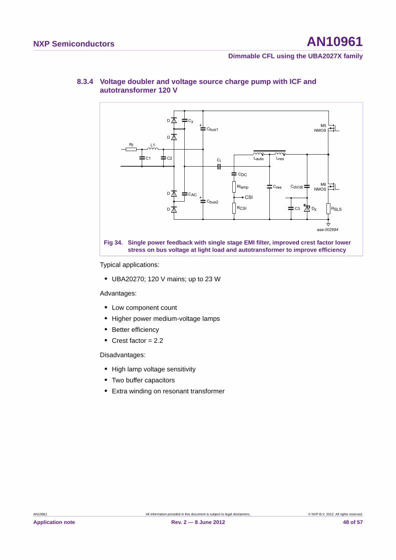
NXP Semiconductors AN10961Dimmable CFL using the UBA2027X family
8.3.4 Voltage doubler and voltage source charge pump with ICF and autotransformer 120 V
Typical applications:
• UBA20270; 120 V mains; up to 23 W
Advantages:
• Low component count
• Higher power medium-voltage lamps
• Better efficiency
• Crest factor = 2.2
Disadvantages:
• High lamp voltage sensitivity
• Two buffer capacitors
• Extra winding on resonant transformer
Fig 34. Single power feedback with single stage EMI filter, improved crest factor lower stress on bus voltage at light load and autotransformer to improve efficiency
���������
��
��
��
�
���
�)#��
�)#��
�!#�' ����
�N �����9
������.
��
7 ��
�
�
�
�
�(
���
�%
����
����
��!"�
���
AN10961 All information provided in this document is subject to legal disclaimers. © NXP B.V. 2012. All rights reserved.
Application note Rev. 2 — 8 June 2012 48 of 57

NXP Semiconductors AN10961Dimmable CFL using the UBA2027X family
8.3.5 Voltage doubler and voltage source current source charge 120 V
Typical applications:
• UBA20270; 120 V mains; up to 23 W
Advantages:
• Low lamp voltage sensitivity
• Suitable for high-voltage lamps
• Crest factor = 1.75
Disadvantages:
• Extra 1:1 current transformer required
Fig 35. Double power feedback with single stage EMI filter and autotransformer to improve efficiency
���������
��
��
��
���
���� ���� ����
�)#��
�)#��
����
�N �����9
�������
��
� ��
��!"�
����
�H�
�N� � �
�� ���
�H�
�(
�N� � �
�%
� �
AN10961 All information provided in this document is subject to legal disclaimers. © NXP B.V. 2012. All rights reserved.
Application note Rev. 2 — 8 June 2012 49 of 57

NXP Semiconductors AN10961Dimmable CFL using the UBA2027X family
8.3.6 Bridge rectified voltage source current source charge pump 120 V
Typical applications:
• UBA20271; 120 V mains; up to 18 W
Advantages:
• Low lamp voltage sensitivity
• Works with low to medium-voltage amalgam lamps
• Less sensitive to parasitic capacitor in coupling from half-bridge output to CSI input Lres
• Good THD
• Crest factor = 1.75
Disadvantages:
• Extra 1:1 current transformer required
Fig 36. Double power feedback with single stage EMI filter
��������
��
��
��
�9 �%
���
����
� �
�)#�
����
�N �����8
�������
��
� ��
��!"�
����� �
�H � � � �
�����
� �
�(
AN10961 All information provided in this document is subject to legal disclaimers. © NXP B.V. 2012. All rights reserved.
Application note Rev. 2 — 8 June 2012 50 of 57

NXP Semiconductors AN10961Dimmable CFL using the UBA2027X family
8.3.7 Bridge rectified voltage source current source charge pump with autotransformer 120 V
Typical applications:
• UBA20271; 120 V mains; up to 18 W
• UBA20270; > 18 W; external MOSFET
Advantages:
• Low lamp voltage sensitivity
• Works with medium to high-voltage amalgam lamps
• High PF (> 0.85)
• Low THD (< 40 %)
• Better efficiency
• Less sensitive to parasitic capacitor coupling from half-bridge output to CSI input, resulting in deeper and stable dimming
• Lower half-bridge current
• Crest factor = 1.75
Disadvantages:
• Extra 1:1 current transformer required
• Extra winding on resonant transformer
Fig 37. Double power feedback with single stage EMI filter and autotransformer to improve efficiency
���������
��
��
��
�8 �%
���
����
� �
�)#�
�!#�' ����
�N �����7
�������
��
� ����!"�
����
� �
�H � � � �
��
�F�
���
� �
�
AN10961 All information provided in this document is subject to legal disclaimers. © NXP B.V. 2012. All rights reserved.
Application note Rev. 2 — 8 June 2012 51 of 57

NXP Semiconductors AN10961Dimmable CFL using the UBA2027X family
8.3.8 Bridge rectified voltage source current source 230 V
Typical applications:
• UBA20272; 230 V mains; up to 18 W
• UBA20270; > 18 W; external MOSFET
Advantages:
• Low lamp voltage sensitivity
• Works with medium to high-voltage amalgam lamps
• High PF (> 0.85)
• Low THD (< 40 %)
• Not sensitive to parasitic capacitor coupling from half-bridge output to CSI input, resulting in deeper and stable dimming
• Crest factor = 1.75
Disadvantages:
• Extra 1:1 current transformer required
Fig 38. Double power feedback with dual-stage EMI filter and autotransformer to improve efficiency
���������
��
�� ��
�� �9
�8 �%
���
����
� �
�)#�
����
�N �����7
�������
��
� ����!"�
����
� �
�H � � � �
��
�F�
���
� �
�
AN10961 All information provided in this document is subject to legal disclaimers. © NXP B.V. 2012. All rights reserved.
Application note Rev. 2 — 8 June 2012 52 of 57

NXP Semiconductors AN10961Dimmable CFL using the UBA2027X family
8.3.9 Bridge rectified voltage source current source charge pump with lamp to ground 230 V
Typical applications:
• UBA20272; 230 V mains; up to 18 W
• UBA20270; > 18 W; external MOSFET
Advantages:
• No extra 1:1 current transformer required
• Good for low to medium-voltage lamps
• Less overpumping
Disadvantages:
• Lamp voltage sensitivity
• Extra inductor required
• Extra winding on resonant transformer required
Fig 39. Double power feedback with dual stage EMI filter, auto and floating current source, no current transformer required and lamp to ground operation
����������
��
�� ��
�� �9
�8 �%
����
����
����
�
�)#�
�%
����
����
�N �����7
�������
��
� ��
����
��!"�
� �
�H � � � �
���� �
�(
AN10961 All information provided in this document is subject to legal disclaimers. © NXP B.V. 2012. All rights reserved.
Application note Rev. 2 — 8 June 2012 53 of 57

NXP Semiconductors AN10961Dimmable CFL using the UBA2027X family
8.3.10 Bridge rectified voltage source current source charge pump with lamp to ground 120 V
Typical applications:
• UBA20271; 120 V mains; up to 18 W
Advantages:
• No extra 1:1 current transformer required
• Good for low-voltage lamps
• Less overpumping
Disadvantages:
• Lamp voltage sensitivity
• Extra inductor required
• Extra winding on resonant transformer required
Fig 40. Double power feedback with single stage EMI filter, auto and floating current source, no current transformer required and lamp to ground operation
���������
��
�� ��
�9 �%
����
����
����
� �
�)#���
����
����
�N �����8
�������
��
� ��
����
��!"�
� �
�H � � � �
���� �
�(
AN10961 All information provided in this document is subject to legal disclaimers. © NXP B.V. 2012. All rights reserved.
Application note Rev. 2 — 8 June 2012 54 of 57
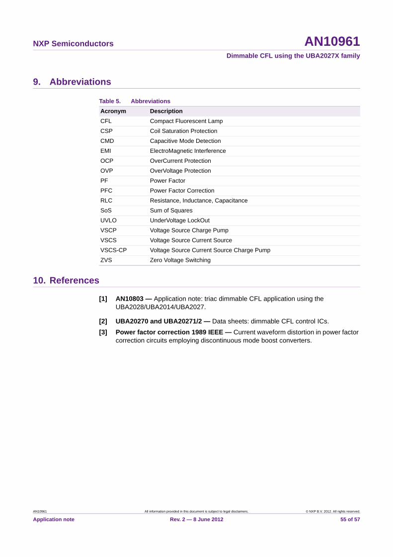
NXP Semiconductors AN10961Dimmable CFL using the UBA2027X family
9. Abbreviations
10. References
[1] AN10803 — Application note: triac dimmable CFL application using the UBA2028/UBA2014/UBA2027.
[2] UBA20270 and UBA20271/2 — Data sheets: dimmable CFL control ICs.
[3] Power factor correction 1989 IEEE — Current waveform distortion in power factor correction circuits employing discontinuous mode boost converters.
Table 5. Abbreviations
Acronym Description
CFL Compact Fluorescent Lamp
CSP Coil Saturation Protection
CMD Capacitive Mode Detection
EMI ElectroMagnetic Interference
OCP OverCurrent Protection
OVP OverVoltage Protection
PF Power Factor
PFC Power Factor Correction
RLC Resistance, Inductance, Capacitance
SoS Sum of Squares
UVLO UnderVoltage LockOut
VSCP Voltage Source Charge Pump
VSCS Voltage Source Current Source
VSCS-CP Voltage Source Current Source Charge Pump
ZVS Zero Voltage Switching
AN10961 All information provided in this document is subject to legal disclaimers. © NXP B.V. 2012. All rights reserved.
Application note Rev. 2 — 8 June 2012 55 of 57

NXP Semiconductors AN10961Dimmable CFL using the UBA2027X family
11. Legal information
11.1 Definitions
Draft — The document is a draft version only. The content is still under internal review and subject to formal approval, which may result in modifications or additions. NXP Semiconductors does not give any representations or warranties as to the accuracy or completeness of information included herein and shall have no liability for the consequences of use of such information.
11.2 Disclaimers
Limited warranty and liability — Information in this document is believed to be accurate and reliable. However, NXP Semiconductors does not give any representations or warranties, expressed or implied, as to the accuracy or completeness of such information and shall have no liability for the consequences of use of such information. NXP Semiconductors takes no responsibility for the content in this document if provided by an information source outside of NXP Semiconductors.
In no event shall NXP Semiconductors be liable for any indirect, incidental, punitive, special or consequential damages (including - without limitation - lost profits, lost savings, business interruption, costs related to the removal or replacement of any products or rework charges) whether or not such damages are based on tort (including negligence), warranty, breach of contract or any other legal theory.
Notwithstanding any damages that customer might incur for any reason whatsoever, NXP Semiconductors’ aggregate and cumulative liability towards customer for the products described herein shall be limited in accordance with the Terms and conditions of commercial sale of NXP Semiconductors.
Right to make changes — NXP Semiconductors reserves the right to make changes to information published in this document, including without limitation specifications and product descriptions, at any time and without notice. This document supersedes and replaces all information supplied prior to the publication hereof.
Suitability for use — NXP Semiconductors products are not designed, authorized or warranted to be suitable for use in life support, life-critical or safety-critical systems or equipment, nor in applications where failure or malfunction of an NXP Semiconductors product can reasonably be expected to result in personal injury, death or severe property or environmental damage. NXP Semiconductors and its suppliers accept no liability for inclusion and/or use of NXP Semiconductors products in such equipment or applications and therefore such inclusion and/or use is at the customer’s own risk.
Applications — Applications that are described herein for any of these products are for illustrative purposes only. NXP Semiconductors makes no representation or warranty that such applications will be suitable for the specified use without further testing or modification.
Customers are responsible for the design and operation of their applications and products using NXP Semiconductors products, and NXP Semiconductors accepts no liability for any assistance with applications or customer product design. It is customer’s sole responsibility to determine whether the NXP Semiconductors product is suitable and fit for the customer’s applications and products planned, as well as for the planned application and use of customer’s third party customer(s). Customers should provide appropriate design and operating safeguards to minimize the risks associated with their applications and products.
NXP Semiconductors does not accept any liability related to any default, damage, costs or problem which is based on any weakness or default in the customer’s applications or products, or the application or use by customer’s third party customer(s). Customer is responsible for doing all necessary testing for the customer’s applications and products using NXP Semiconductors products in order to avoid a default of the applications and the products or of the application or use by customer’s third party customer(s). NXP does not accept any liability in this respect.
Export control — This document as well as the item(s) described herein may be subject to export control regulations. Export might require a prior authorization from competent authorities.
Evaluation products — This product is provided on an “as is” and “with all faults” basis for evaluation purposes only. NXP Semiconductors, its affiliates and their suppliers expressly disclaim all warranties, whether express, implied or statutory, including but not limited to the implied warranties of non-infringement, merchantability and fitness for a particular purpose. The entire risk as to the quality, or arising out of the use or performance, of this product remains with customer.
In no event shall NXP Semiconductors, its affiliates or their suppliers be liable to customer for any special, indirect, consequential, punitive or incidental damages (including without limitation damages for loss of business, business interruption, loss of use, loss of data or information, and the like) arising out the use of or inability to use the product, whether or not based on tort (including negligence), strict liability, breach of contract, breach of warranty or any other theory, even if advised of the possibility of such damages.
Notwithstanding any damages that customer might incur for any reason whatsoever (including without limitation, all damages referenced above and all direct or general damages), the entire liability of NXP Semiconductors, its affiliates and their suppliers and customer’s exclusive remedy for all of the foregoing shall be limited to actual damages incurred by customer based on reasonable reliance up to the greater of the amount actually paid by customer for the product or five dollars (US$5.00). The foregoing limitations, exclusions and disclaimers shall apply to the maximum extent permitted by applicable law, even if any remedy fails of its essential purpose.
Non-automotive qualified products — Unless this data sheet expressly states that this specific NXP Semiconductors product is automotive qualified, the product is not suitable for automotive use. It is neither qualified nor tested in accordance with automotive testing or application requirements. NXP Semiconductors accepts no liability for inclusion and/or use of non-automotive qualified products in automotive equipment or applications.
In the event that customer uses the product for design-in and use in automotive applications to automotive specifications and standards, customer (a) shall use the product without NXP Semiconductors’ warranty of the product for such automotive applications, use and specifications, and (b) whenever customer uses the product for automotive applications beyond NXP Semiconductors’ specifications such use shall be solely at customer’s own risk, and (c) customer fully indemnifies NXP Semiconductors for any liability, damages or failed product claims resulting from customer design and use of the product for automotive applications beyond NXP Semiconductors’ standard warranty and NXP Semiconductors’ product specifications.
11.3 TrademarksNotice: All referenced brands, product names, service names and trademarks are the property of their respective owners.
AN10961 All information provided in this document is subject to legal disclaimers. © NXP B.V. 2012. All rights reserved.
Application note Rev. 2 — 8 June 2012 56 of 57

NXP Semiconductors AN10961Dimmable CFL using the UBA2027X family
12. Contents
1 Introduction . . . . . . . . . . . . . . . . . . . . . . . . . . . . 3
2 Scope . . . . . . . . . . . . . . . . . . . . . . . . . . . . . . . . . 3
3 Triac dimming . . . . . . . . . . . . . . . . . . . . . . . . . . 43.1 Triac dimmer circuit . . . . . . . . . . . . . . . . . . . . . 43.1.1 Circuit overview . . . . . . . . . . . . . . . . . . . . . . . . 43.2 Triac wall dimmer with VSCS charge pump
and CFL ballast . . . . . . . . . . . . . . . . . . . . . . . . 5
4 Application design. . . . . . . . . . . . . . . . . . . . . . . 84.1 Simplified circuit diagram . . . . . . . . . . . . . . . . . 84.2 Resonant tank parameters . . . . . . . . . . . . . . . . 94.3 Autotransformer . . . . . . . . . . . . . . . . . . . . . . . 104.4 Voltage source current source charge pump . 114.5 Inductive mode preheating and Sum of
Squares (SoS) . . . . . . . . . . . . . . . . . . . . . . . . 144.6 Dimming using frequency feedback
control loop . . . . . . . . . . . . . . . . . . . . . . . . . . . 184.7 CI integrator circuit and differential feedback . 204.8 Boosting of the lamp. . . . . . . . . . . . . . . . . . . . 224.9 Setting Minimum Dimming Level (MDL) . . . . . 234.10 IC supply and capacitive mode protection . . . 234.10.1 Capacitive mode protection . . . . . . . . . . . . . . 244.11 Mains input filtering. . . . . . . . . . . . . . . . . . . . . 254.12 Extra protections. . . . . . . . . . . . . . . . . . . . . . . 274.12.1 OverPower Protection (OPP) . . . . . . . . . . . . . 274.12.2 Coil Saturation Protection (CSP)
and OverCurrent Protection (OCP). . . . . . . . . 274.13 End of life circuit (optional) . . . . . . . . . . . . . . . 284.14 23 W 120 V dimmable CFL schematic
with UBA20270. . . . . . . . . . . . . . . . . . . . . . . . 294.15 23 W 230 V PF dimmable CFL schematic
with UBA20270. . . . . . . . . . . . . . . . . . . . . . . . 304.16 18 W maximum 120 V dimmable CFL
schematic with UBA20271 . . . . . . . . . . . . . . . 314.17 18 W maximum 230 V dimmable CFL
schematic with UBA20272 . . . . . . . . . . . . . . . 32
5 Appendix 1: Power calculations. . . . . . . . . . . 335.1 VSCS-CP with enhanced conduction angle
design equations . . . . . . . . . . . . . . . . . . . . . . 335.2 Assumptions . . . . . . . . . . . . . . . . . . . . . . . . . . 335.3 Lamp current crest factor . . . . . . . . . . . . . . . . 345.4 Current stress in output stage steady state
mode (burn state) . . . . . . . . . . . . . . . . . . . . . . 345.5 DC bus voltage stress during burn state. . . . . 345.6 DC bus voltage stress during ignition state . . 355.7 Average input line current and power over
one switching cycle. . . . . . . . . . . . . . . . . . . . . 35
6 Appendix 2: New NXP VSCP pump topology 37
7 Appendix 3: Inductive mode preheat calculations . . . . . . . . . . . . . . . . . . . . . . . . . . . 38
8 Appendix 4: Cook book . . . . . . . . . . . . . . . . . 418.1 Selection variables. . . . . . . . . . . . . . . . . . . . . 418.1.1 Nominal burner voltage . . . . . . . . . . . . . . . . . 418.1.2 Burner power . . . . . . . . . . . . . . . . . . . . . . . . . 418.1.3 IC dissipation . . . . . . . . . . . . . . . . . . . . . . . . . 428.1.4 Circuit topology . . . . . . . . . . . . . . . . . . . . . . . 428.2 Selection guides. . . . . . . . . . . . . . . . . . . . . . . 438.3 Application diagrams . . . . . . . . . . . . . . . . . . . 458.3.1 Bridge rectified voltage source charge
pump with ICF 120 V . . . . . . . . . . . . . . . . . . . 458.3.2 Bridge rectified voltage source charge
pump with ICF and autotransformer 120 V . . 468.3.3 Voltage doubler and voltage source charge
pump with ICF 120 V . . . . . . . . . . . . . . . . . . . 478.3.4 Voltage doubler and voltage source charge
pump with ICF and autotransformer 120 V . . 488.3.5 Voltage doubler and voltage source current
source charge 120 V . . . . . . . . . . . . . . . . . . . 498.3.6 Bridge rectified voltage source current
source charge pump 120 V . . . . . . . . . . . . . . 508.3.7 Bridge rectified voltage source current
source charge pump with autotransformer 120 V . . . . . . . . . . . . . . . . . . . . . . . . . . . . . . . 51
8.3.8 Bridge rectified voltage source current source 230 V . . . . . . . . . . . . . . . . . . . . . . . . . 52
8.3.9 Bridge rectified voltage source current s ource charge pump with lamp to ground 230 V . . . . . . . . . . . . . . . . . . . . . . . . . . . . . . . 53
8.3.10 Bridge rectified voltage source current source charge pump with lamp to ground 120 V . . . . . . . . . . . . . . . . . . . . . . . . . . . . . . . 54
9 Abbreviations . . . . . . . . . . . . . . . . . . . . . . . . . 55
10 References. . . . . . . . . . . . . . . . . . . . . . . . . . . . 55
11 Legal information . . . . . . . . . . . . . . . . . . . . . . 5611.1 Definitions . . . . . . . . . . . . . . . . . . . . . . . . . . . 5611.2 Disclaimers . . . . . . . . . . . . . . . . . . . . . . . . . . 5611.3 Trademarks . . . . . . . . . . . . . . . . . . . . . . . . . . 56
12 Contents. . . . . . . . . . . . . . . . . . . . . . . . . . . . . . 57
© NXP B.V. 2012. All rights reserved.
For more information, please visit: http://www.nxp.com For sales office addresses, please send an email to: [email protected]
Date of release: 8 June 2012
Document identifier: AN10961
Please be aware that important notices concerning this document and the product(s) described herein, have been included in section ‘Legal information’.