AN009: CC1000/CC1050 Microcontroller...
20
Application Note AN009 AN009 CC1000/CC1050 Microcontroller interfacing By K. H. Torvmark Keywords CC1000 CC1050 Microchip PIC Atmel AVR Example code Configuration interface Data interface Calibration Averaging filter Introduction The CC1000 RF transceiver is very easy to interface with a microcontroller. The chip is configured using a three-wire bus, comprising of PCLK, PDATA and PALE signals. Data interfacing is done via the DCLK and DIO pins. Three different modes for interfacing with a microcontroller are available. Please note that everything in this document also applies to the CC1050, except where noted. Data decision and synchronisation is done by the CC1000, easing the workload of the microcontroller considerably. Using the synchronous Manchester or NRZ modes, the CC1000 supplies a synchronous clock, which can be used for triggering interrupts in the microcontroller, or for interfacing with a synchronous serial interface. The SWRA082 Page 1 of 20
Transcript of AN009: CC1000/CC1050 Microcontroller...

Application
Note AN009
AN009CC1000/CC1050 Microcontroller interfacing
By K. H. Torvmark
Keywords
CC1000 CC1050 Microchip PIC Atmel AVR Example code
Configuration interface Data interface Calibration Averaging filter
Introduction
The CC1000 RF transceiver is very easy to interface with a microcontroller.
The chip is configured using a three-wire bus, comprising of PCLK, PDATA and PALE signals.
Data interfacing is done via the DCLK and DIO pins. Three different modes for interfacing with a microcontroller are available.
Please note that everything in this document also applies to the CC1050, except where noted.
Data decision and synchronisation is done by the CC1000, easing the workload of the microcontroller considerably. Using the
synchronous Manchester or NRZ modes, the CC1000 supplies a synchronous clock, which can be used for triggering interrupts in the microcontroller, or for interfacing with a synchronous serial interface. The transparent UART mode can be used for connecting the CC1000 to a UART.
This application note covers interfacing the CC1000 to microcontrollers. Information is given about both the configuration and data interfaces of the CC1000.
In addition, this application note covers details of how to utilize the CC1000’s averaging filter and calibration functions.
SWRA082 Page 1 of 14

Application
Note AN009
Microcontrollers in generalA vast variety of microcontrollers (MCUs) exist today, from small 4-bit controllers up to powerful 32-bit controllers with processing power rivalling modern PCs. Digital signal processors (DSPs) are also used as controllers in some applications.
The CC1000 can be easily interfaced with any microcontroller now on the market. The only requirement is to have enough free I/O pins. To configure the CC1000, three I/O pins are required (one bi-directional and two output pins). The pins connected to PDATA and PLCK can be shared with other circuitry, providing these circuits are not active when the configuration interface is active. The ALE signal must be driven by pin dedicated only to interfacing the CC1000. For the data interface, two I/O pins are required, one for DIO (bi-directional for the CC1000, output for the CC1050) and one for DCLK (input). The pin used to interface with DCLK should be able to generate an interrupt on signal edges.
Figure 1 CC1000 – MCU hardware interfaceIf the number of I/O pins used is critical, you can reduce the number of pins required by using the same pins for the configuration interface and the data interface. A minimal setup will look like this:
Figure 2: Minimal CC1000 - MCU hardware interface
SWRA082 Page 2 of 14

Application
Note AN009
Using this connection, DIO and PDATA are connected together using a resistor. The same is done with DCLK and PCLK. MCU pin usage is reduced to 3 pins, but you cannot use the configuration and data interfaces at the same time. Chipcon recommends using the connections in Figure 1 if possible. The resistor value will depend on the drive capability of the I/O pins of the MCU.In power-down mode, the CC1000 pins assume the following states:
Pin Pin state NotePDATA InputPCLK InputPALE Input with internal pull-
up resistorShould be driven high or high-impedance to minimize power consumption
DIO InputDCLK High-impedance
output
Figure 3: CC1000 pins in power-down mode
Configuration interfaceThe CC1000 is configured using the PCLK, PDATA and PALE signals. This is discussed in detail in the CC1000 data sheet. The configuration registers are also readable, so that the user can verify settings and read out status bits.
Using general-purpose I/O pins to handle an interface in this way is often called “bit banging”. This approach is very flexible, as the user is free to use any I/O pins on the microcontroller, but can be slow when working with a slow microcontroller.
The alternative is to use a synchronous serial interface to interface with the CC1000. An SPI master interface or some types of USART (Universal Synchronous/Asynchronous Receiver/Transmitter) are suitable. When interfacing with an SPI master, the MISO and MOSI pins should be connected together. The MOSI pin should be configured as an input when reading from the CC1000. A free general I/O pin can be used to interface with the PALE pin of the CC1000. Please note that some microcontroller manufacturers use different terminologies when naming the signals. MOSI stands for master out, slave in, while MISO stands for master in, slave out. The other standard SPI signals are SCK (Serial Clock) and SS (Slave select). SS is not used when interfacing the CC1000 with an SPI interface.
SWRA082 Page 3 of 14

Application
Note AN009
Figure 4: Suggested SPI configuration interfacing
A USART or other synchronous serial interface can be suitable for use as well, study the datasheet for the microcontroller to see if it can be configured to be compatible with the CC1000.
The biggest advantage of using a hardware interface is that it can be much faster; in many cases the configuration can be performed with a clock rate of several MHz. This is especially important in frequency hopping applications, where configuration must occur in the blanking interval, which should be as short as possible.
The CHP_OUT pin need not be connected to a microcontroller, its use is entirely optional. The CC1000 can be configured to provide several different signals on this pin, the most interesting are: LOCK_CONTINUOUS (PLL lock indicator), TX_PDB (can be used to control an external PA), Manchester violation and RX_PDB (can be used to control an external LNA). The use of the pin is controlled by the LOCK register, please see the data sheet for more details.
The RSSI/IF pin is also optional. An analogue RSSI signal is available at this pin; it is controlled by the IF_RSSI bits in the FRONT_END register. The RSSI should be turned off when not in use, as the RSSI circuitry consumes around 0.3mA in receive mode.
If RSSI is used, it should be connected to an A/D converter, many microcontrollers have this as a built-in peripheral. The RSSI output ranges between 1.2 and 0 V when the recommended 27 kΩ terminating resistor is used. See the datasheet for further details.
Configuration procedureChipcon recommends resetting the CC1000 (by clearing the RESET_N bit in the MAIN register) when the chip is first powered up. All registers that need to be configured should then be programmed (those which differ from their default values). Registers can be programmed freely in any order. The CC1000 should then be calibrated in both RX and TX mode. After this is complete, the CC1000 is ready for use. See the datasheet for detailed procedure flowcharts.
SWRA082 Page 4 of 14

Application
Note AN009
SmartRF® Studio and the example code written by Chipcon assumes that frequency register A is used for the RX frequency, and frequency register B is used for the TX frequency. This makes it easy to switch between RX and TX mode by programming the MAIN, PLL and CURRENT registers.
For the CC1050, both registers are used for TX. Having two frequency registers is still very useful in a multi-channel or frequency hopping system.
Data interfaceWhen using the Synchronous Manchester or the Synchronous NRZ mode, the DCLK pin on the CC1000 should be connected to an input pin that can generate an interrupt in the MCU. DIO should be connected to a bi-directional I/O pin.
In TX mode, the interrupt should be triggered on the falling edge of DCLK. When the interrupt occurs, write the next bit to be transmitted to the I/O pin. In RX mode, the interrupt should be triggered on the rising edge of DCLK. When the interrupt occurs, read the data from the I/O pin.
Note that data transferred to/from the MCU is always NRZ coded, regardless of whether Synchronous NRZ or Synchronous Manchester mode is selected. The mode setting only affects the signal modulated onto the RF carrier. The Manchester encoding/decoding is performed by the CC1000.
The DCLK signal will be output a clock as long as the CC1000 is not in power-down mode. If transmissions are intermittent, the user must implement a software squelch scheme to determine whether valid data is received. In Manchester mode, the Manchester violation flag available at the CHP_OUT pin is useful for this. To read this signal, set LOCK_SELECT=1001 in the LOCK register, and connect an MCU input pin to the CHP_OUT pin of the CC1000.
A preamble of alternate ones and zeros must be used regardless of which mode the CC1000 is in. See the datasheet for details regarding minimum length of the preamble.
For information about higher-level issues with data interfacing, please see AN015. This application note presents a complete working system using either of the NRZ and Manchester modes. [3] presents a more detailed view of protocol design.
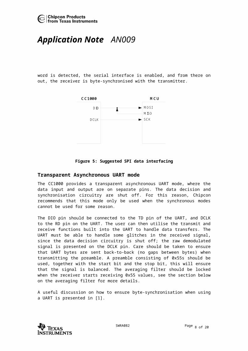
The data interface can also be connected to a synchronous serial interface in the same way as the configuration interface. In this case, since the CC1000 provides the DCLK signal, the microcontroller must act as a slave. If an SPI interface is used, the MISO signal pin must be set as an input when reading data from the CC1000. If using the CC1050, the DI pin may be connected directly to the MOSI pin of the SPI interface, and the MISO pin can be left unconnected. When receiving, byte synchronisation must be handled by the microcontroller software. This involves detecting a start-of-frame (SOF) unique identifier, which is sent after the preamble. When this word is detected, the serial interface is enabled, and from there on out, the receiver is byte-synchronised with the transmitter.
SWRA082 Page 5 of 14

Application
Note AN009
Figure 5: Suggested SPI data interfacing
Transparent Asynchronous UART modeThe CC1000 provides a transparent asynchronous UART mode, where the data input and output are on separate pins. The data decision and synchronisation circuitry are shut off. For this reason, Chipcon recommends that this mode only be used when the synchronous modes cannot be used for some reason.
The DIO pin should be connected to the TD pin of the UART, and DCLK to the RD pin on the UART. The user can then utilise the transmit and receive functions built into the UART to handle data transfers. The UART must be able to handle some glitches in the received signal, since the data decision circuitry is shut off; the raw demodulated signal is presented on the DCLK pin. Care should be taken to ensure that UART bytes are sent back-to-back (no gaps between bytes) when transmitting the preamble. A preamble consisting of 0x55s should be used, together with the start bit and the stop bit, this will ensure that the signal is balanced. The averaging filter should be locked when the receiver starts receiving 0x55 values, see the section below on the averaging filter for more details.
A useful discussion on how to ensure byte-synchronisation when using a UART is presented in [1].
SWRA082 Page 6 of 14

Application
Note AN009
The averaging filterThis section is not relevant to the CC1050.
The averaging filter provides a slicing level for the data slicer in the demodulator. The filter can be locked, allowing the CC1000 to work with data that is not DC-balanced.
If Synchronous Manchester mode is used, the bit slicer averaging filter should be left free-running, and does not need to be locked manually. Each message must still start with a preamble, so that the averaging filter can acquire the proper DC level and the data synchroniser can synchronise to the exact data rate. The length of the preamble depends on the settling time of the filter; see the CC1000 data sheet for values.
In applications such as frequency hopping, locking the averaging filter may be advantageous, even when using Manchester mode. When the filter is locked, the averaging filter does not need to settle after a frequency hop. Only bit synchronisation must have time to settle, this can be handled by using a short preamble of around 8 bauds.
If Synchronous NRZ or Transparent Asynchronous UART mode is used, the filter must be locked either manually or automatically. If a polling receiver is being implemented, the filter can be set up for automatic lock, as shown in Figure 6. Please note that the automatic lock is not intelligent; i.e. it does not detect valid data in any way. The automatic lock locks the filter n bauds after the CC1000 has entered RX mode. n can be found in the settling table in the data sheet.
Figure 6 Locking the averaging filter automaticallyIf the CC1000 stays in received mode while searching for a preamble, manual lock should be used, as shown in Figure 7. The filter is left free running until a valid preamble has been detected, then it must be locked manually.
SWRA082 Page 7 of 14
Application
Note AN009
Figure 7 Locking the averaging filter manuallyThe filter should be unlocked again after the message has been received. When the averaging filter has been locked, the value is retained even when switching into TX or power-down mode.
SWRA082 Page 8 of 14

Application
Note AN009
VCO and PLL Self-calibrationThe CC1000 includes a calibration function, which calibrates the charge pump current and the VCO capacitance array. The CC1000 must be calibrated at start-up (when power is applied, it does not have to be calibrated when it has been in power-down mode), and it must be recalibrated when:
The frequency is changed by more than 1 MHz The supply voltage has changed by more than 0.5V The temperature has changed by more than 40°C
The calibration is initiated by writing a 1 into the CAL_START bit. The CAL_COMPLETE bit will change to 1 once the calibration is finished. The CAL_START bit must then be set to 0 again. Calibration time is nominally 28ms when running on an 11.052 MHz crystal. The calibration should be performed as a single calibration (CAL_DUAL=0 in CAL register), so that separate values are used for frequency registers A and B.
The calibration values are stored separately for each frequency register when single calibration is used. Therefore, in a single-channel application, it is sufficient to calibrate once in RX and once in TX when the system is powered up. Once this is done, the system can change between RX and TX by writing to the MAIN, PLL and CURRENT registers, and no recalibration needs to be performed unless one of the recalibration requirements above occur.
Please note that the synthesiser, bias and crystal oscillator core must be powered up for the calibration to work.
To calibrate, a value of 0xA6 must be written to the CAL register. The program should then wait until the CAL_COMPLETE bit goes high, and then write a value of 0x26 to the CAL register. When calibrating in TX mode, the PA should be turned off (PA_POW register set to 0x00) in order to prevent frequency spatter during the calibration.
Calibration values can also be read out again and stored, this is useful in a frequency-hopping protocol, for example. The calibration values are read out of the TEST0 and TEST2 registers. Note that when using single calibration, calibration values are stored separately for frequency registers A and B. This means that the TEST0 and TEST2 registers will contain calibration settings for the currently selected frequency register (selected by F_REG in the MAIN register). To write the calibration values back, make sure the proper frequency register is selected, and write the values into TEST5 and TEST6, respectively. Note that you must set VCO_OVERRIDE=1 in TEST5 and CHP_OVERRIDE=1 in the TEST6 register. To end overriding of the calibration values, VCO=OVERRIDE and CHP_OVERRIDE must both be set to 0.
SWRA082 Page 9 of 14

Application
Note AN009
Packet-level operationA RF packet should generally consist of the following:
Preamble 010101010101… - see datasheet for minimum length SOF (Start-of-frame), also called a synchronisation word. This does several things; it
helps determine where the preamble stops, it uniquely identifies your system and helps you to distinguish your data from noise, and it helps you perform byte alignment. If you do not use a CRC, this should be 2 bytes long to keep the false-message rate down, otherwise 1 byte will be sufficient.
Your data, which can be of any form you like. Addressing, packet counters and CRCs are recommended to make for a stable protocol. See [3] for more information about protocol design.
Receiving packets in NRZ or Manchester mode
1. Search for the preamble. This is most easily done by simply shifting the data into a shift register, and then comparing the register to 0xAA and 0x55. Once you have one of these values, you go on to the next step.2. Declare a tentative "preamble detected" (set a flag or something), and continue shifting in data. If you're in NRZ mode, lock the averaging filter now. Compare the data to your SOF (start-of-frame, a unique ID which is sent at the start of your data stream), if you find this, go to the next step. If not, compare it to 0xAA and 0x55. If it isn't equal to one of these, you have an error. You may want to tolerate a few errors here, but if you get several, give up and go back to step 1.3. OK, you've found your SOF. Depending on the application, you may want to add another byte of SOF (if you have problems with noise showing up as data). If you do this, compare the data to your second byte of SOF, go back to 1 if it does not match.4. Done! You now know you are receiving valid data. If your data packets are of variable size, you can either add a size field in the packet header, or have a specific end-of-packet marker. Just make sure to handle it gracefully if this info should be subject to bit errors. A CRC checksum at the end of the packet is a good idea, you can then discard or retransmit the data according to the needs of your application.
If you are in the Manchester mode, you'll probably want to include the Manchester violation bit as well to the above procedure, if you get a violation, you can count it as an error. The Manchester violation signal (available at the CHP_OUT pin if you set the LOCK register correctly) is updated each bit (just as the DIO pin), the threshold for declaring a violation can be set in the MODEM1 register. The Manchester violation flag is an additional piece of information to use in the procedure, and should not be used by itself.
The procedure above is applicable to an application where you are in receive mode looking for data all the time. If you are doing polling, awakening at intervals to see if there is any data, you should limit the time you spend in step 1, going back to sleep if you don't find a preamble after a suitable amount of time.
Receiving packets in UART mode
In UART mode, there are some issues regarding detection of preamble, locking of averaging filter, and byte synchronization you need to consider:
SWRA082 Page 10 of 14

Application
Note AN009
1. Search for the preamble. This is most easily done by searching for 0xAA and 0x55. Once you have one of these values, you go on to the next step.2. Manually lock the averaging filter.3. Byte-alignment. See [1] for more information on this. Disregard the constraint/comment regarding the maximum number of consecutive 0's and 1's. In CC1000 there is no constraint with respect to the link being moderately balanced because you have locked the averaging filter in 1) above (the preamble must be dc balanced). 4. Depending on the application, you may want to add another byte of SOF (if you have problems with noise showing up as data). If you do this, compare the data to your byte of SOF, go back to 1 if it does not match.5. Done! You now know you are receiving valid data. If your data packets are of variable size, you can either add a size field in the packet header, or have a specific end-of-packet marker. Just make sure to handle it gracefully if this info should be subject to bit errors. A CRC checksum at the end of the packet is a good idea, you can then discard or retransmit the data according to the needs of your application.
The procedure above is applicable to an application where you are in receive mode looking for data all the time. If you are doing polling, awakening at intervals to see if there is any data, you should limit the time you spend in step 1, going back to sleep if you don't find a preamble after a suitable amount of time.
Since only raw data is provided in UART mode, synchronization or decoding must be done by the UART. Make sure that the UART does proper oversampling and that it can handle the jitter the RF communication introduces.
SWRA082 Page 11 of 14
Application
Note AN009
Microchip PIC16 exampleThis example is written for the PIC16F876 microcontroller, using the RF Modem hardware. See [2] for more information about the hardware. Application note AN015 also shows a complete protocol including byte synchronisation and preamble/start-of-frame detection.
cc1000.c provides a library of routines for configuring the CC1000. cc1000.h contains definitions for all of the CC1000’s registers. There are two versions of the low-level configuration routines, one using general-purpose I/O and one using the SPI interface built into the PIC. If the symbol ‘SPI’ is defined, the SPI versions are used, if not, the general-purpose I/O routines are used. The PIC must be set up properly for the routines to work, please see [2] for a complete example.
A short description of the routines in the library follows:
ConfigureCC1000() takes an array and a count value as input parameters. The array should be filled with values of the short int type (16 bits) consisting of a valid CC1000 register address in the 7 highest bits, and the register value in the lowest 8 bits. The count value should be set equal to the number of values stored in the array.
WriteToCC1000Register() takes an address and a value as parameters, and writes to a single CC1000 register.
ReadFromCC1000Register() takes an address of a CC1000 register as parameter, and returns the value of that register.
Several higher-level routines are included as well:CalibrateCC1000() initiates a calibration, and waits for it to finish. It also turns off the PA before initiating calibration, which prevents spurious transmission from occurring in TX mode. The PA is turned back on once calibration is completed.ResetCC1000() resets all the CC1000 registers to defaults.
When the system is initially turned on, the CC1000 should first be reset. The registers can then be programmed to the settings used in the system. The CC1000 should be calibrated in both RX and TX modes before system operation takes place. When the CC1000 is awakened from PD mode, the power consumption can be minimised by only turning on the crystal oscillator at first, then waiting until it has stabilised (2-5ms) before turning the rest of the transceiver on. This is implemented in the WakeUpCC1000ToTX() and WakeUpCC1000ToRX() routines. For details, see the CC1000 data sheet.
SWRA082 Page 12 of 14

Application
Note AN009
Atmel AVR exampleThis example is written for the Atmel ATmega8L microcontroller. The microcontroller should be connected to a CC1000PP module as shown in the figure below.
Figure 8: AVR-CC1000 connectionsThis set up can be tested using an ATmega8L in DIP package plugged into the Atmel STK500 development board. A CC1000PP module can then be connected to the pin headers on the development board using a cable. Just modify the pin definitions at the start of the file with the pins you have selected.
The AVR is fast compared to most other 8-bit microcontrollers, so in many applications bit-banging the interfaces using general I/O pins is appropriate. Often, it will be advantageous to handle RF communications via interrupts. If this is required, the DCLK signal should be connected to one of the external interrupt pins of the AVR.
If the CC1000 is to be run at very high data rates, it is a good idea to use the SPI interface of the ATmega8 to handle the CC1000s data interface. In this case, byte synchronisation will have to be handled as explained earlier in this document.
CC1000avr.c provides the same set out configuration routines for the CC1000 as the PIC example. Make sure to modify the TX_CURRENT, RX_CURRENT, TX_PLL, RX_PLL and PA_VALUE constants with values for your application. Use SmartRF® Studio to calculate these values.
All source code can be downloaded from the Chipcon website (www.chipcon.com).
SWRA082 Page 13 of 14

Application
Note AN009
References[1] Robert V. Ammerman: “Ensuring byte synchronisation for ASYNC over RF”.
PICLIST, http://www.piclist.com/techref/microchip/ammermansync.htm[2] Chipcon: Application Note AN015 RF Modem Reference Design. www.chipcon.com[3] Karl H. Torvmark: “Short Range Wireless Design”. Embedded Systems
Programming, October 2002 p. 20.
This application note is written by the staff of Chipcon to the courtesy of our customers. Chipcon is a world-wide distributor of integrated radio transceiver chips. For further information on the products from Chipcon please contact us or visit our web site.
Contact Information
Address: Chipcon ASGaustadalléen 21N-0349 Oslo, NORWAY
Telephone : (+47) 22 95 85 44Fax : (+47) 22 95 85 46E-mail : [email protected] site : http://www.chipcon.com
Disclaimer
Chipcon AS believes the furnished information is correct and accurate at the time of this printing. However, Chipcon AS reserves the right to make changes to this application note without notice. Chipcon AS does not assume any responsibility for the use of the described information. Please refer to Chipcon’s web site for the latest update.
SWRA082 Page 14 of 14