Antenna II LN07_Reflector Antennas [email protected] 1 /34 Reflector Antennas.
AN INVESTIGATION OF ON-CHIP ANTENNA CHARACTERISTICS RELATED TO
ENERGY HARVESTING APPLICATIONS
by
Dmitry Gorodetsky
B.Sc. in Electrical Engineering, University of Pittsburgh, 1999
Submitted to the Graduate Faculty of
the School of Engineering in partial fulfillment
of the requirements for the degree of
Master of Science in Electrical Engineering
University of Pittsburgh
2002

ii
UNIVERSITY OF PITTSBURGH
SCHOOL OF ENGINEERING
This dissertation was presented
by
Dmitry Gorodetsky
It was defended on
May 3, 2002
and approved by
Dr. Marlin H. Mickle, Professor, Electrical Engineering
Dr. Raymond R. Hoare, Assistant Professor, Electrical Engineering
Dr. J.T. Cain, Professor, Electrical Engineering
Dr. Ronald G. Hoelzeman, Associate Professor, Electrical Engineering
Dr. Marlin H. Mickle Dissertation Director

iii
ABSTRACT
AN INVESTIGATION OF ON-CHIP ANTENNA CHARACTERISTICS RELATED TO ENERGY HARVESTING APPLICATIONS
Dmitry Gorodetsky, M.Sc.
University of Pittsburgh, 2002
The way a certain antenna operates is highly dependent on the dielectric medium in
which it is placed. Dielectric media can be characterized by their dielectric constant, which is
also called relative permittivity. When no electric field is applied, the positive and negative
charges of the dielectric molecules are evenly distributed. Application of an electric field
disrupts this balance and results in the creation of dipoles. The number of dipoles that are
created is proportional to the permittivity of the dielectric. Permittivity is a measure of the
sensitivity of the material to an applied electric field. Stated another way, permittivity is a
measure of how much energy can be stored in the electric field.
This thesis reports the research on several types of on-the-chip antennas such as a
rectangular spiral and a rectangular patch. The characteristics of these antennas that are useful to
Energy Harvesting are analyzed and the effects of permittivity changes in the dielectrics
surrounding the antenna are studied.

iv
TABLE OF CONTENTS 1.0 Introduction......................................................................................................................... 1
1.1 Motivation............................................................................................................................ 1 1.2 RFID Basics ......................................................................................................................... 1 1.3 CMOS Process ..................................................................................................................... 2 1.4 Small Antennas .................................................................................................................... 3 1.5 Size and Application Limitations......................................................................................... 5
2.0 Statement of the Problem.................................................................................................... 6 3.0 Antenna Fundamentals........................................................................................................ 7
3.1 Radiation Pattern.................................................................................................................. 7 3.2 Radiation Intensity, Directivity, and Gain ......................................................................... 10 3.3 Efficiency........................................................................................................................... 11 3.4 Input Impedance................................................................................................................. 11 3.5 Bandwidth .......................................................................................................................... 13
4.0 CMOS Process Fundamentals........................................................................................... 15 4.1 Physical Geometry ............................................................................................................. 15 4.2 Silicon Substrate ................................................................................................................ 16 4.3 Oxide.................................................................................................................................. 17 4.4 Metal .................................................................................................................................. 18
5.0 Design Tools ..................................................................................................................... 19 5.1 Ansoft................................................................................................................................. 19 5.2. ASITIC.............................................................................................................................. 25
6.0 Testing Procedures............................................................................................................ 25 6.1 Rig...................................................................................................................................... 25 6.2 Network Analyzer.............................................................................................................. 26
7.0 Patch - Theory................................................................................................................... 26 7.1 Background........................................................................................................................ 26 7.2 Frequency........................................................................................................................... 29 7.3 Bandwidth and Radiating Efficiency ................................................................................. 32
8.0 Patch – Simulations........................................................................................................... 33 8.1 Introduction........................................................................................................................ 33 8.2 Microstrip with Intrinsic Silicon........................................................................................ 34 8.3 Microstrip with Doped Silicon........................................................................................... 38 8.4 Microstrip with Substrate Oxide and Doped Silicon ......................................................... 41 8.5 Chip with Sub and Superstrates and Doped Silicon .......................................................... 43 8.6 Variation of Superstrate Oxide Permittivity ...................................................................... 45 8.7 Variation of Substrate Oxide Permittivity ......................................................................... 46
9.0 Square Spiral – Simulations.............................................................................................. 48 9.1 Introduction........................................................................................................................ 48 9.2 Variation of Substrate Oxide Permittivity ......................................................................... 52

v
9.3 Variation of Superstrate Oxide Permittivity ...................................................................... 53 10.0 Summary and Conclusions ............................................................................................... 54 BIBLIOGRAPHY......................................................................................................................... 59

vi
LIST OF FIGURES Figure 1.1 RFID the old way. ........................................................................................................ 2 Figure 1.2 Chip Photograph........................................................................................................... 2 Figure 1.3 Chip Diagram ............................................................................................................... 3 Figure 1.4 Microstrip and On-chip Antennas ................................................................................ 5 Figure 1.5 Wirebonder ................................................................................................................... 6 Figure 3.1 Antenna orientation. ..................................................................................................... 8 Figure 3.2 Example 3-D E-Field Pattern ....................................................................................... 9 Figure 3.3 Coordinate System Used with Antennas. ................................................................... 14 Figure 4.1 Spiral Ridges .............................................................................................................. 16 Figure 4.2 Chip Geometry ........................................................................................................... 18 Figure 5.1 Models Possible with Ensemble................................................................................. 20 Figure 5.2 Sample 2-D Radiation Pattern .................................................................................... 21 Figure 5.3 Ensemble Meshing Example ...................................................................................... 22 Figure 5.4 Example of HFSS Meshing ........................................................................................ 23 Figure 5.5 Port depiction.............................................................................................................. 24 Figure 6.1 Test Rig ...................................................................................................................... 26 Figure 6.2 Network Analyzer ...................................................................................................... 26 Figure 7.1 Patch geometry ........................................................................................................... 27 Figure 7.2 Chip Layer Diagram for Patch. .................................................................................. 29 Figure 8.1 Patch Details (all units in µm.). .................................................................................. 34 Figure 8.2 Input Impedance ......................................................................................................... 35 Figure 8.3 Magnitude of Reflection Coefficient.......................................................................... 36 Figure 8.4 Gain Pattern with Undoped Silicon (unitless). ........................................................... 37 Figure 8.5 Input Impedance with and without Doping ................................................................ 39 Figure 8.6 Gain Pattern with Doped Silicon (unitless). ............................................................... 40 Figure 8.7 Geometry for Simulation............................................................................................ 41 Figure 8.8 Input Impedance with Substrate Oxide ...................................................................... 42 Figure 8.9 Geometry for Simulation............................................................................................ 43 Figure 8.10 Chip Antenna Input Impedance................................................................................ 44 Figure 8.11 Resonant Frequency as a Function of Superstrate Permittivity................................ 45 Figure 8.12 Input Impedance with Superstrate Permittivity of 13.4............................................ 46 Figure 8.13 Resonant Frequency as a Function of Substrate Oxide Permittivity........................ 47 Figure 8.14 Input Impedance with Substrate Permittivity of 5.0................................................. 48 Figure 9.1 Square Spiral Top View. ............................................................................................ 49 Figure 9.2 Spiral Geometry Side View........................................................................................ 49 Figure 9.3 Spiral Antenna with a Via to Ground ......................................................................... 50 Figure 9.4 Effect of Middle Via................................................................................................... 50 Figure 9.5 Input Impedance of Spiral Antenna (no via). ............................................................. 51

vii
Figure 9.6 Effects of Changing the Substrate Permittivity. ......................................................... 52 Figure 9.7 Effects of Changing the Superstrate Permittivity....................................................... 53
1
1.0 Introduction
1.1 Motivation
The motivation for the research that has led to this work has been the demand for smaller
and less expensive devices in the radio frequency identification (RFID) arena. RFID involves
the identification of items via electromagnetic waves in the RF region of the spectrum. This
technology is similar to barcodes but instead of “printed barcodes”, special attachable or
embedded tags are placed on or in each object to be identified. The basics of this process are
outlined below.
1.2 RFID Basics
The base station or scanner sends an RF signal to power the tag. The remotely powered
tag processes certain information and modulates an RF signal that sends back information to the
base station. The scanning process with RFID is similar to scanning with barcodes. The
disadvantages of barcodes that are remedied by RFID are that the barcode scanner has to be in
closer proximity with a more constrained orientation. The location of the barcode must be
visible to the scanner. Another advantage of RFID is that the tag placed on each item can be
reprogrammed with new information at any point whereas the barcode is only printed once.
In order for the tag to work as outlined above, it must consist of a receiving antenna,
some electronics, and a transmitting antenna, which may be shared with the receiving antenna.
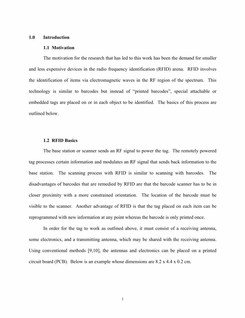
Using conventional methods [9,10], the antennas and electronics can be placed on a printed
circuit board (PCB). Below is an example whose dimensions are 8.2 x 4.4 x 0.2 cm.
2
Figure 1.1 RFID the old way.
The drawbacks of the approach outlined above are the relatively large footprint and
power required to run the on-board electronics. Both of these disadvantages can be overcome by
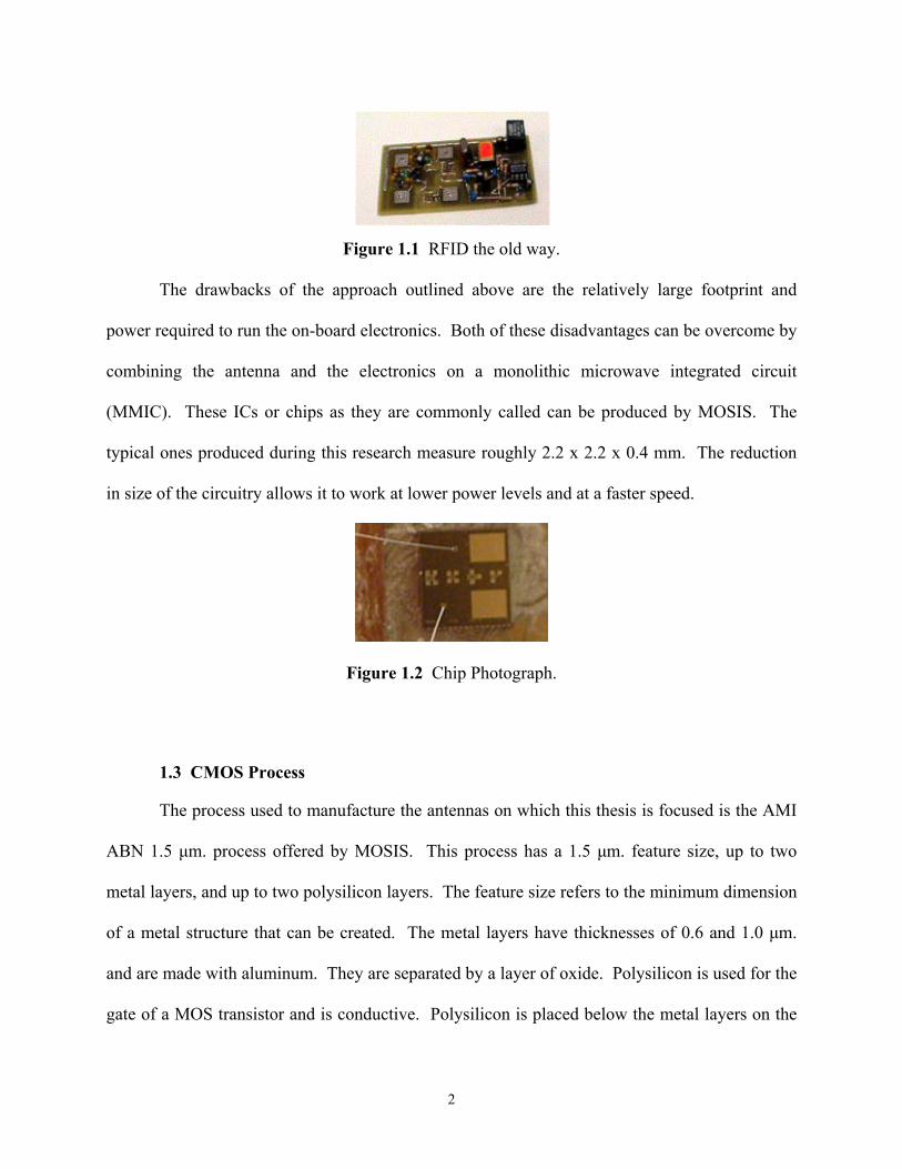
combining the antenna and the electronics on a monolithic microwave integrated circuit
(MMIC). These ICs or chips as they are commonly called can be produced by MOSIS. The
typical ones produced during this research measure roughly 2.2 x 2.2 x 0.4 mm. The reduction
in size of the circuitry allows it to work at lower power levels and at a faster speed.
Figure 1.2 Chip Photograph.
1.3 CMOS Process
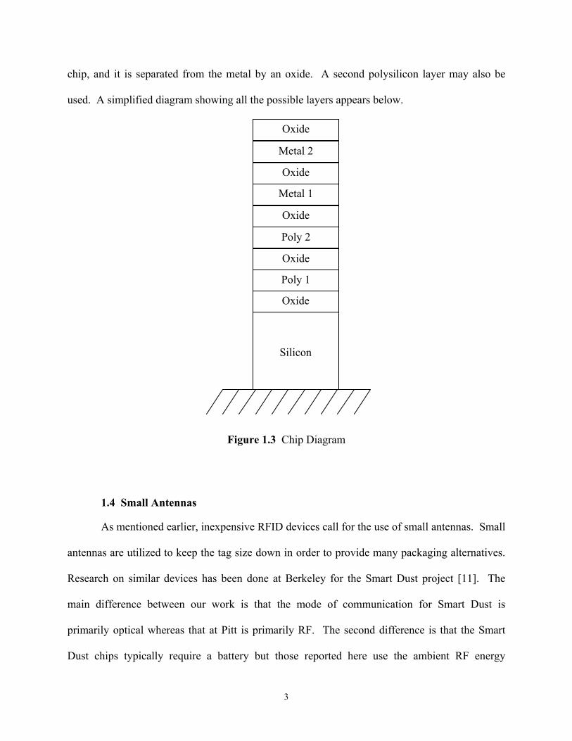
The process used to manufacture the antennas on which this thesis is focused is the AMI
ABN 1.5 µm. process offered by MOSIS. This process has a 1.5 µm. feature size, up to two
metal layers, and up to two polysilicon layers. The feature size refers to the minimum dimension
of a metal structure that can be created. The metal layers have thicknesses of 0.6 and 1.0 µm.
and are made with aluminum. They are separated by a layer of oxide. Polysilicon is used for the
gate of a MOS transistor and is conductive. Polysilicon is placed below the metal layers on the
3
chip, and it is separated from the metal by an oxide. A second polysilicon layer may also be
used. A simplified diagram showing all the possible layers appears below.
Figure 1.3 Chip Diagram
1.4 Small Antennas
As mentioned earlier, inexpensive RFID devices call for the use of small antennas. Small
antennas are utilized to keep the tag size down in order to provide many packaging alternatives.
Research on similar devices has been done at Berkeley for the Smart Dust project [11]. The
main difference between our work is that the mode of communication for Smart Dust is
primarily optical whereas that at Pitt is primarily RF. The second difference is that the Smart
Dust chips typically require a battery but those reported here use the ambient RF energy
Oxide
Silicon
Poly 1
Poly 2
Oxide
Oxide
Metal 1
Metal 2
Oxide
Oxide
4
propagated through the air as a source of power. Self-powered nodes are studied in another
Berkeley project called “PicoRadio” but instead of RF they use sources such as solar energy,
vibrations, and acoustic noise [15]. Investigations of low-power sensing devices similar to Smart
Dust are also being conducted at the UCLA Wireless Integrated Network Sensors Project
(WINS) and the Ultra Low Power Wireless Sensor Project at MIT [12, 13].
The research in microstrip antennas has been the driving force of the miniaturization of
antennas. As mentioned in [5], the trend started with the introduction of microstrip transmission
lines in the 1950s. Soon it became very clear that these lines suffered from radiation losses and
other parasitic effects, which became worse with frequency. Years later the concept of
microstrip antennas emerged where the designer was concerned with maximizing these radiation
losses. Microstrip antennas usually have planar configurations. They are very compact and easy
to manufacture. One advantage is that because of the antenna’s simple geometry, it can be
manufactured in a non-planar configuration to conform to the curved surfaces of objects on
which it is mounted [6]. These can be the surfaces of vehicles, missiles, etc. Another attractive
advantage of these antennas is that they can easily be manufactured on integrated circuits.
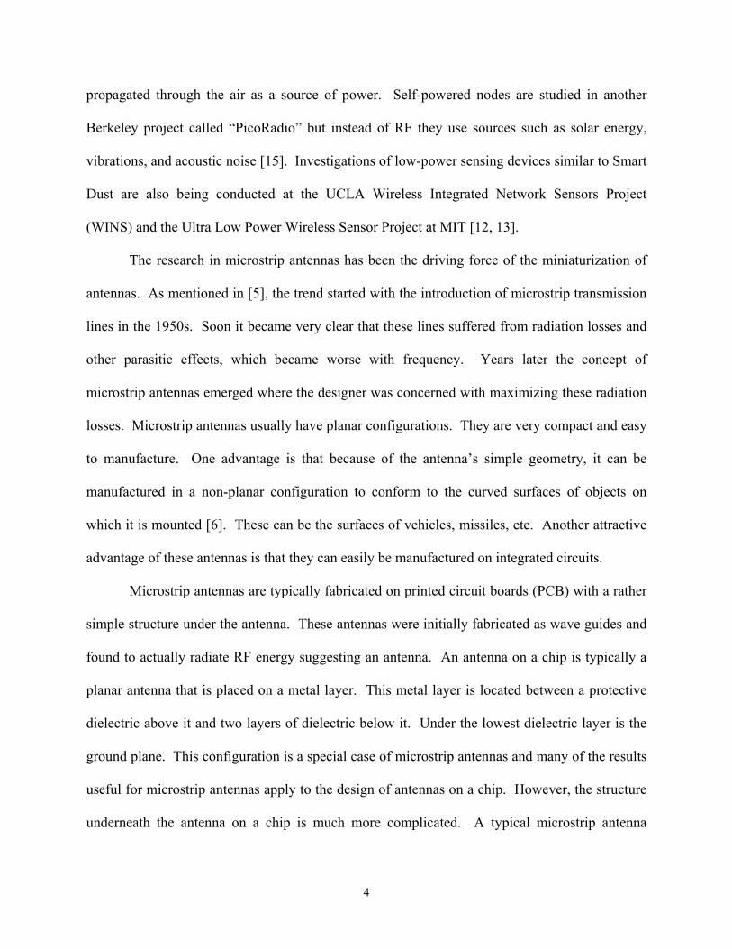
Microstrip antennas are typically fabricated on printed circuit boards (PCB) with a rather
simple structure under the antenna. These antennas were initially fabricated as wave guides and
found to actually radiate RF energy suggesting an antenna. An antenna on a chip is typically a
planar antenna that is placed on a metal layer. This metal layer is located between a protective
dielectric above it and two layers of dielectric below it. Under the lowest dielectric layer is the
ground plane. This configuration is a special case of microstrip antennas and many of the results
useful for microstrip antennas apply to the design of antennas on a chip. However, the structure
underneath the antenna on a chip is much more complicated. A typical microstrip antenna
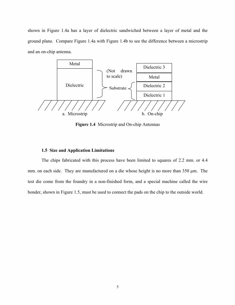
5
shown in Figure 1.4a has a layer of dielectric sandwiched between a layer of metal and the
ground plane. Compare Figure 1.4a with Figure 1.4b to see the difference between a microstrip
and an on-chip antenna.
a. Microstrip b. On-chip
Figure 1.4 Microstrip and On-chip Antennas
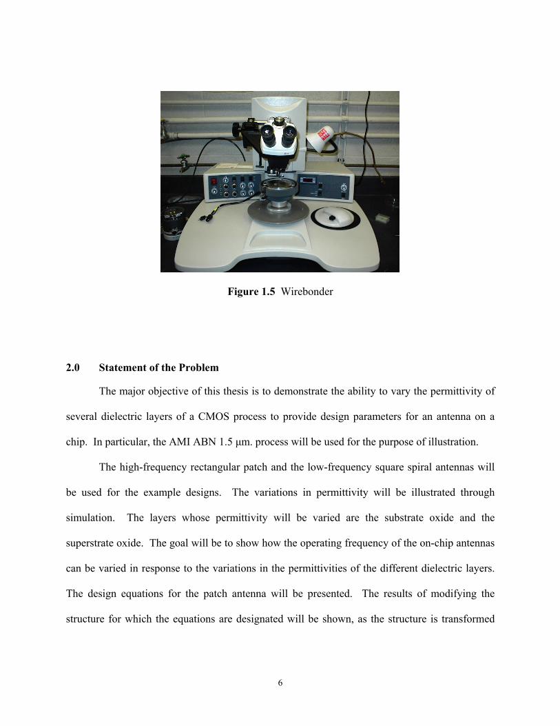
1.5 Size and Application Limitations
The chips fabricated with this process have been limited to squares of 2.2 mm. or 4.4
mm. on each side. They are manufactured on a die whose height is no more than 350 µm. The
test die come from the foundry in a non-finished form, and a special machine called the wire
bonder, shown in Figure 1.5, must be used to connect the pads on the chip to the outside world.
SubstrateDielectric 1
Metal
Dielectric 2
Dielectric 3
Dielectric
Metal (Not drawn to scale)
6
Figure 1.5 Wirebonder
2.0 Statement of the Problem
The major objective of this thesis is to demonstrate the ability to vary the permittivity of
several dielectric layers of a CMOS process to provide design parameters for an antenna on a
chip. In particular, the AMI ABN 1.5 µm. process will be used for the purpose of illustration.
The high-frequency rectangular patch and the low-frequency square spiral antennas will
be used for the example designs. The variations in permittivity will be illustrated through
simulation. The layers whose permittivity will be varied are the substrate oxide and the
superstrate oxide. The goal will be to show how the operating frequency of the on-chip antennas
can be varied in response to the variations in the permittivities of the different dielectric layers.
The design equations for the patch antenna will be presented. The results of modifying the
structure for which the equations are designated will be shown, as the structure is transformed

7
from a microstrip to an on-chip antenna. The permittivity variations in the dielectric layers will
also be shown for the spiral antenna.
Permittivity of a dielectric is a measure of its ability to store charge. A change of the
relative permittivity of a dielectric surrounding an antenna can be shown to have an effect on the
antenna’s resonant frequency. In doing this, care must be taken not to disturb the other
characteristics that make this structure an antenna.
The indices for evaluation will be the reflection coefficient, the input impedance, antenna
gain, and efficiency. Based on the information from the input impedance curves, the antenna’s
resonant frequency will be extracted.
3.0 Antenna Fundamentals
3.1 Radiation Pattern
The radiation pattern of an antenna is an important characteristic that will represent
graphically one of the radiation properties of the antenna as a function of space coordinates. The
properties that can be shown are the power flux density, radiation intensity, field strength,
directivity phase, and polarization [1]. Usually these plots are made on a spherical surface of a
constant radius r away from the antenna centered at the origin. The coordinate system used is
shown in the figure below, which displays a dipole antenna.
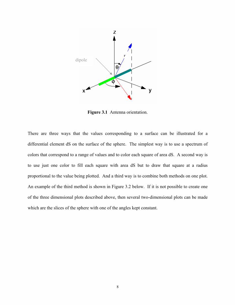
8
Figure 3.1 Antenna orientation.
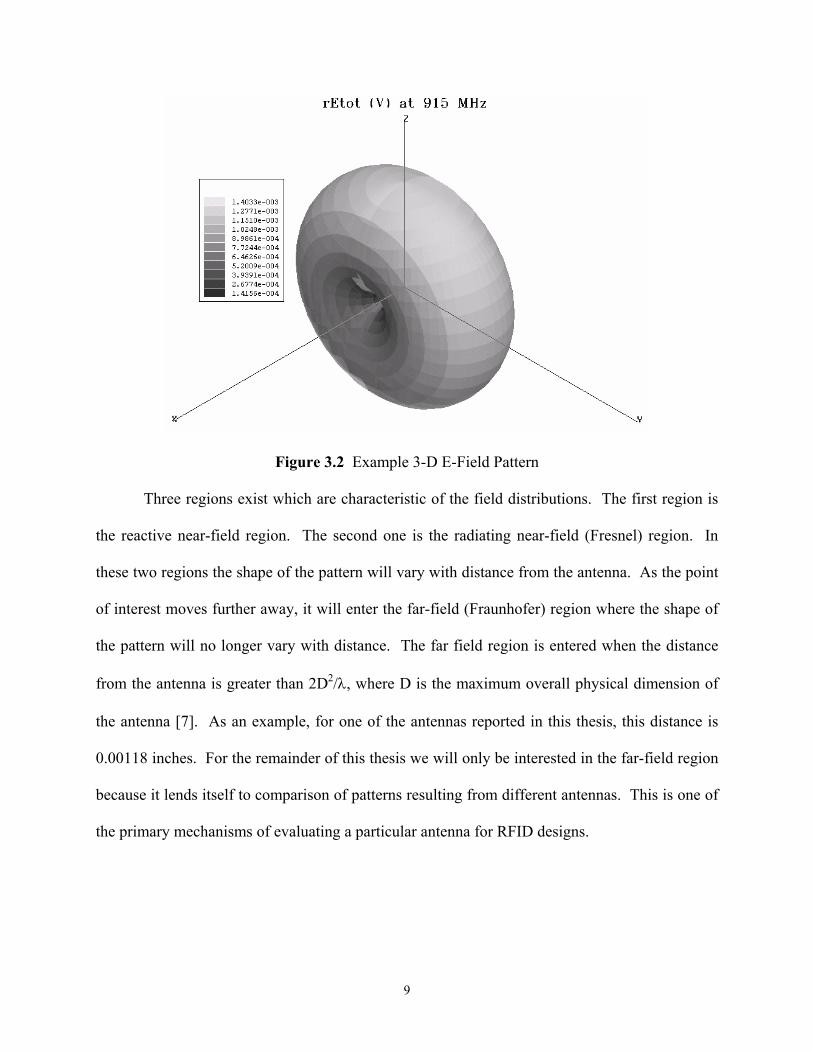
There are three ways that the values corresponding to a surface can be illustrated for a
differential element dS on the surface of the sphere. The simplest way is to use a spectrum of
colors that correspond to a range of values and to color each square of area dS. A second way is
to use just one color to fill each square with area dS but to draw that square at a radius
proportional to the value being plotted. And a third way is to combine both methods on one plot.
An example of the third method is shown in Figure 3.2 below. If it is not possible to create one
of the three dimensional plots described above, then several two-dimensional plots can be made
which are the slices of the sphere with one of the angles kept constant.
rdipole
9
Figure 3.2 Example 3-D E-Field Pattern
Three regions exist which are characteristic of the field distributions. The first region is
the reactive near-field region. The second one is the radiating near-field (Fresnel) region. In
these two regions the shape of the pattern will vary with distance from the antenna. As the point
of interest moves further away, it will enter the far-field (Fraunhofer) region where the shape of
the pattern will no longer vary with distance. The far field region is entered when the distance
from the antenna is greater than 2D2/λ, where D is the maximum overall physical dimension of
the antenna [7]. As an example, for one of the antennas reported in this thesis, this distance is
0.00118 inches. For the remainder of this thesis we will only be interested in the far-field region
because it lends itself to comparison of patterns resulting from different antennas. This is one of
the primary mechanisms of evaluating a particular antenna for RFID designs.
10
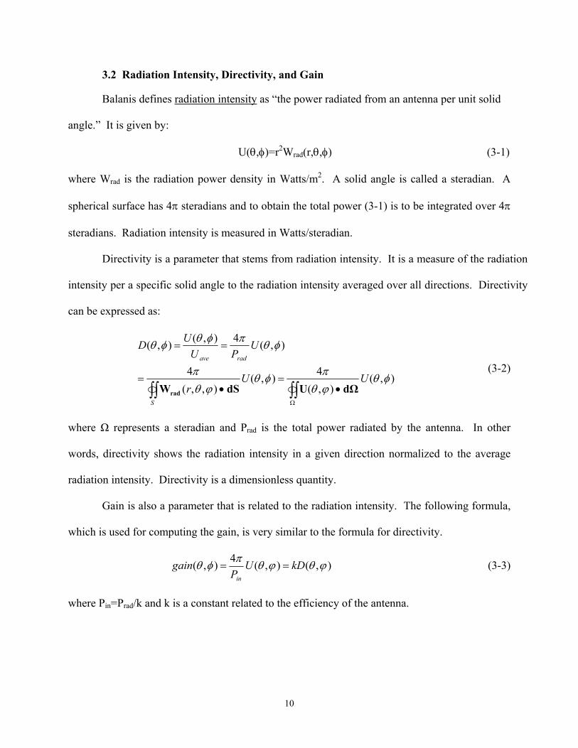
3.2 Radiation Intensity, Directivity, and Gain
Balanis defines radiation intensity as “the power radiated from an antenna per unit solid
angle.” It is given by:
U(θ,φ)=r2Wrad(r,θ,φ) (3-1)
where Wrad is the radiation power density in Watts/m2. A solid angle is called a steradian. A
spherical surface has 4π steradians and to obtain the total power (3-1) is to be integrated over 4π
steradians. Radiation intensity is measured in Watts/steradian.
Directivity is a parameter that stems from radiation intensity. It is a measure of the radiation
intensity per a specific solid angle to the radiation intensity averaged over all directions. Directivity
can be expressed as:
),(),(
4),(),,(
4
),(4),(),(
φθϕθπφθ
ϕθπ
φθπφθφθ
UUr
UPU
UD
S
radave
∫∫∫∫Ω
•=
•=
==
dΩUdSWrad
(3-2)
where Ω represents a steradian and Prad is the total power radiated by the antenna. In other
words, directivity shows the radiation intensity in a given direction normalized to the average
radiation intensity. Directivity is a dimensionless quantity.
Gain is also a parameter that is related to the radiation intensity. The following formula,
which is used for computing the gain, is very similar to the formula for directivity.
),(),(4),( ϕθϕθπφθ kDUP
gainin
== (3-3)
where Pin=Prad/k and k is a constant related to the efficiency of the antenna.

11
Just like directivity, gain is a dimensionless quantity. It should be clear that a plot of gain would
account for the losses of the antenna while a plot of directivity will only show its directional
properties.
3.3 Efficiency
An antenna will have losses at the feed input terminals and it will also have losses due to
the conducting material from which it is constructed and due to the dielectric such as a substrate
in a microstrip antenna. Balanis expresses the overall efficiency of the antenna, eo by:
eo=ereced (3-4)
where
er = reflection efficiency = (1-|Γ|2)
ec = conduction efficiency
ed = dielectric efficiency
0
0
ZZZZ
IN
IN
+−
=Γ , and ZIN is the input impedance of the antenna looking into the feed and Z0
is the characteristic impedance of the feed.
3.4 Input Impedance
The antenna input impedance, ZA, usually refers to the impedance seen looking into the
terminals of the antenna. This is different from ZIN, because ZIN = ZA + ZFEED. The antenna
impedance has a real and an imaginary component and is given by:
ZA(f) = RA(f) + jXA(f) (3-5)

12
The input resistance, which is the real part of the antenna input impedance, will usually consist
of two components, RL, the loss resistance of the antenna and Rr, the radiation resistance of the
antenna. According to many authors, these two components appear in series [1, 7, 8].
The maximum power transfer theorem states that in order to obtain maximum power
from an antenna, its input impedance (ZIN) must be a conjugate of the load’s impedance. When
this is achieved, half of the power will be absorbed in the antenna and half will be utilized in the
load.
After the maximum power transfer theorem has been satisfied, the next step is to limit the
power losses within the antenna. This can be done by minimizing RL and maximizing Rr. In
other words, this is an adjustment of the efficiency of the antenna.
To compute the impedance seen looking into a lossy feed of length L, the following
formula from transmission line theory is used:
++
=LLγtanhγtanh
0
00
A
AIN ZZ
ZZZZ (3-6)
where
Z0 = characteristic impedance of the feed (transmission line)
ZA = antenna input impedance (defined in (3-5))
γ = α + jβ
−
+= 11
2
2
ωεσµεωα
+
+= 11
2
2
ωεσµεωβ
After careful analysis of (3-6), it becomes apparent that if the characteristic impedance and the
antenna input impedance are equal, the term in brackets becomes unity and the input impedance
seen is just Z0. In this case the length of the feed becomes irrelevant to the impedance seen at its

13
terminals. This is the condition of perfect matching of the load to the line. When this occurs, all
power is absorbed by the load and there is no reflection. Usually in RF work the transmission
lines are designed so that their characteristic impedance is real at the specified frequency. The
value of the characteristic impedance is typically 50 or 75 ohms. It is this mechanism that
enables the connection of multiple units using standard coaxial cables.
3.5 Bandwidth
The bandwidth specification of an antenna is a concept not as simple as that characteristic
of a filter for example. In an antenna there are many properties which were described above
such as the radiation pattern, the input impedance, and the efficiency. The variation of these
properties with frequency is usually very different from each other. The bandwidth can be
specified as a range of frequencies where one of these properties is within limits. For instance,
in a dipole antenna the bandwidth is usually determined by the impedance curve since the far
field pattern changes less rapidly [7], making it a more difficult criterion to be specified.
For a dipole, the electric field has two components, in the r and the φ directions as was
shown in Figure 3.1, which is repeated below.
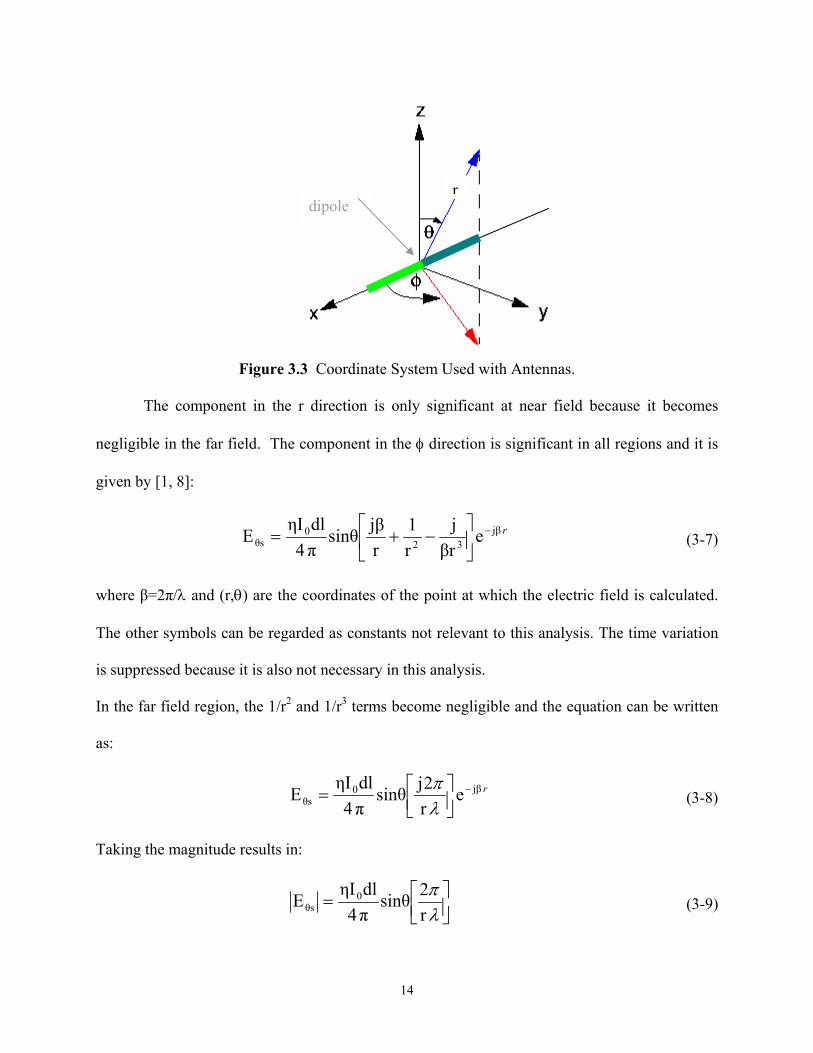
14
Figure 3.3 Coordinate System Used with Antennas.
The component in the r direction is only significant at near field because it becomes
negligible in the far field. The component in the φ direction is significant in all regions and it is
given by [1, 8]:
rjβ32
0θs e
βrj
r1
rjβsinθ
π4dlηIE −
−+= (3-7)
where β=2π/λ and (r,θ) are the coordinates of the point at which the electric field is calculated.
The other symbols can be regarded as constants not relevant to this analysis. The time variation
is suppressed because it is also not necessary in this analysis.
In the far field region, the 1/r2 and 1/r3 terms become negligible and the equation can be written
as:
rjβ0θs e
r2jsinθ
π4dlηIE −
=
λπ
(3-8)
Taking the magnitude results in:
=λπ
r2sinθ
π4dlηIE 0
θs (3-9)
dipole r
15
An alternative form for the radiation resistance of the dipole is given in [1, 8] as:
2
280
=λ
π dlRrad (3-10)
A comparison of (3-9) and (3-10) shows that the electrical field is inversely proportional to the
wavelength while the radiation resistance is inversely proportional to the square of the
wavelength. Therefore, the variation in the electric field with frequency is slower than it is in the
radiation resistance.
The antennas under consideration are to be fabricated on Complementary Metal Oxide
Semiconductor (CMOS) chips. The next section presents the necessary background material for
the development of the antenna design and simulation on a CMOS chip.
4.0 CMOS Process Fundamentals
4.1 Physical Geometry
The AMI ABN process exists primarily for the manufacture of on-chip CMOS and bi-
polar transistors. When these transistors are laid out, they require a complex array of layers and
manufacturing steps. Since we are interested in laying out planar antennas on one metal layer,
the resulting geometry is simpler than that for transistors. Therefore, when we model the patch,
the dielectric above it can all be assumed to be at the same height. In the spiral, however, more
dielectric will cover the areas that have metal than those areas that don’t. This happens because
of the technology used in this process. This will result in the top surface of the dielectric having
an uneven height.
16
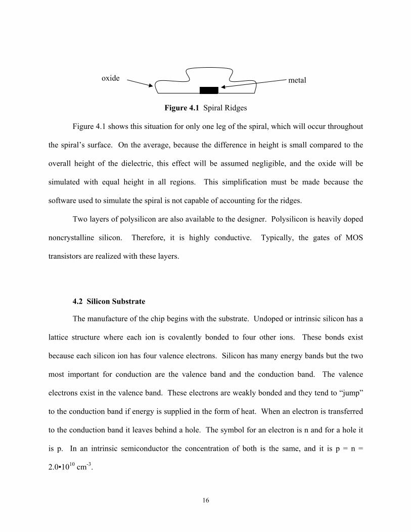
Figure 4.1 Spiral Ridges
Figure 4.1 shows this situation for only one leg of the spiral, which will occur throughout
the spiral’s surface. On the average, because the difference in height is small compared to the
overall height of the dielectric, this effect will be assumed negligible, and the oxide will be
simulated with equal height in all regions. This simplification must be made because the
software used to simulate the spiral is not capable of accounting for the ridges.
Two layers of polysilicon are also available to the designer. Polysilicon is heavily doped
noncrystalline silicon. Therefore, it is highly conductive. Typically, the gates of MOS
transistors are realized with these layers.
4.2 Silicon Substrate
The manufacture of the chip begins with the substrate. Undoped or intrinsic silicon has a
lattice structure where each ion is covalently bonded to four other ions. These bonds exist
because each silicon ion has four valence electrons. Silicon has many energy bands but the two
most important for conduction are the valence band and the conduction band. The valence
electrons exist in the valence band. These electrons are weakly bonded and they tend to “jump”
to the conduction band if energy is supplied in the form of heat. When an electron is transferred
to the conduction band it leaves behind a hole. The symbol for an electron is n and for a hole it
is p. In an intrinsic semiconductor the concentration of both is the same, and it is p = n =
2.0•1010 cm-3.
metal oxide
17
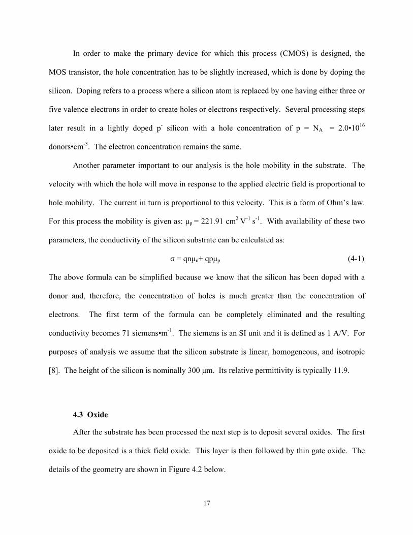
In order to make the primary device for which this process (CMOS) is designed, the
MOS transistor, the hole concentration has to be slightly increased, which is done by doping the
silicon. Doping refers to a process where a silicon atom is replaced by one having either three or
five valence electrons in order to create holes or electrons respectively. Several processing steps
later result in a lightly doped p- silicon with a hole concentration of p = NA = 2.0•1016
donors•cm-3. The electron concentration remains the same.
Another parameter important to our analysis is the hole mobility in the substrate. The
velocity with which the hole will move in response to the applied electric field is proportional to
hole mobility. The current in turn is proportional to this velocity. This is a form of Ohm’s law.
For this process the mobility is given as: µp = 221.91 cm2 V-1 s-1. With availability of these two
parameters, the conductivity of the silicon substrate can be calculated as:
σ = qnµn+ qpµp (4-1)
The above formula can be simplified because we know that the silicon has been doped with a
donor and, therefore, the concentration of holes is much greater than the concentration of
electrons. The first term of the formula can be completely eliminated and the resulting
conductivity becomes 71 siemens•m-1. The siemens is an SI unit and it is defined as 1 A/V. For
purposes of analysis we assume that the silicon substrate is linear, homogeneous, and isotropic
[8]. The height of the silicon is nominally 300 µm. Its relative permittivity is typically 11.9.
4.3 Oxide
After the substrate has been processed the next step is to deposit several oxides. The first
oxide to be deposited is a thick field oxide. This layer is then followed by thin gate oxide. The
details of the geometry are shown in Figure 4.2 below.
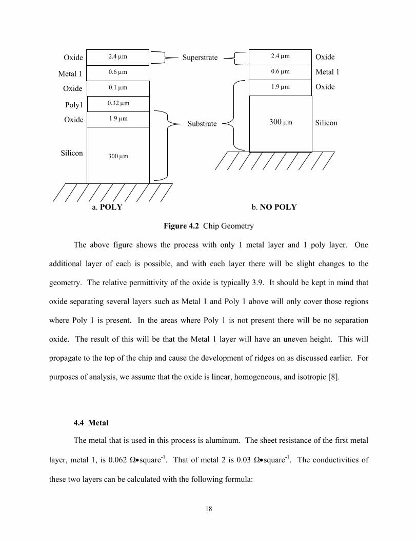
18
a. POLY b. NO POLY
Figure 4.2 Chip Geometry
The above figure shows the process with only 1 metal layer and 1 poly layer. One
additional layer of each is possible, and with each layer there will be slight changes to the
geometry. The relative permittivity of the oxide is typically 3.9. It should be kept in mind that
oxide separating several layers such as Metal 1 and Poly 1 above will only cover those regions
where Poly 1 is present. In the areas where Poly 1 is not present there will be no separation
oxide. The result of this will be that the Metal 1 layer will have an uneven height. This will
propagate to the top of the chip and cause the development of ridges on as discussed earlier. For
purposes of analysis, we assume that the oxide is linear, homogeneous, and isotropic [8].
4.4 Metal
The metal that is used in this process is aluminum. The sheet resistance of the first metal
layer, metal 1, is 0.062 Ω•square-1. That of metal 2 is 0.03 Ω•square-1. The conductivities of
these two layers can be calculated with the following formula:
1.9 µm
300 µm Silicon
Oxide
0.32 µm Poly1
0.6 µm Metal 1
2.4 µm Oxide
0.1 µm Oxide
Superstrate
Substrate
1.9 µm
0.6 µm
Silicon
Oxide
Metal 1
2.4 µm Oxide
300 µm

19
HRS
1=σ (4-2)
where
RS = sheet resistance [Ω•square-1] H = height of metal [meters]
The effect of sheet resistance becomes clear from the following:
WLR
WL
HR STotal ==
ρ (4-3)
where
ρ = σ -1 = resistivity [Ω•m•square-1]
When a choice must be made which metal layer to use, the one with the lower sheet resistance
will give the lowest total resistance, i.e. metal 2. To compare the conductivities calculated for
the silicon, the conductivity of metal 1 is 2.69•107 siemens•m-1 and that of metal 2 is 3.33•107
siemens•m-1.
5.0 Design Tools
5.1 Ansoft
The theoretical analysis involved in the design of some antennas can become quite
involved, and in many cases an exact solution may not be possible. This is the point where
electromagnetic analysis software comes in. This software provides a graphical display of the
radiating characteristics of an antenna as well as the input impedance given by (3-5). A plot at
one frequency of interest can be produced or many different frequencies can be swept.
The two programs produced by Ansoft Corporation that are used for dynamic
electromagnetic analysis are Ensemble and HFSS. Dynamic quantities are those that vary with
20
time versus static which do not. As an aside, electromagnetic wave propagation can only be
achieved for time-varying electric fields. Static electric fields, analyzed by another Ansoft
software product called Maxwell cannot produce electromagnetic waves that propagate through
space.
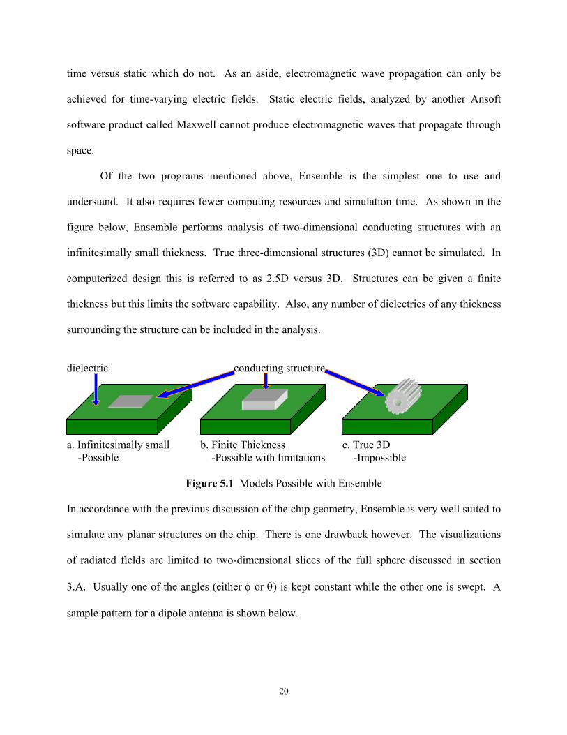
Of the two programs mentioned above, Ensemble is the simplest one to use and
understand. It also requires fewer computing resources and simulation time. As shown in the
figure below, Ensemble performs analysis of two-dimensional conducting structures with an
infinitesimally small thickness. True three-dimensional structures (3D) cannot be simulated. In
computerized design this is referred to as 2.5D versus 3D. Structures can be given a finite
thickness but this limits the software capability. Also, any number of dielectrics of any thickness
surrounding the structure can be included in the analysis.
dielectric conducting structure
a. Infinitesimally small b. Finite Thickness c. True 3D -Possible -Possible with limitations -Impossible
Figure 5.1 Models Possible with Ensemble
In accordance with the previous discussion of the chip geometry, Ensemble is very well suited to
simulate any planar structures on the chip. There is one drawback however. The visualizations
of radiated fields are limited to two-dimensional slices of the full sphere discussed in section
3.A. Usually one of the angles (either φ or θ) is kept constant while the other one is swept. A
sample pattern for a dipole antenna is shown below.
21
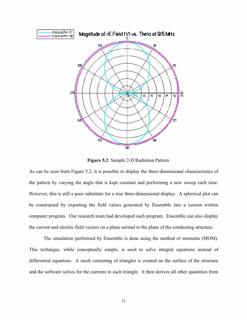
Figure 5.2 Sample 2-D Radiation Pattern
As can be seen from Figure 5.2, it is possible to display the three-dimensional characteristics of
the pattern by varying the angle that is kept constant and performing a new sweep each time.
However, this is still a poor substitute for a true three-dimensional display. A spherical plot can
be constructed by exporting the field values generated by Ensemble into a custom written
computer program. Our research team had developed such program. Ensemble can also display
the current and electric field vectors on a plane normal to the plane of the conducting structure.
The simulation performed by Ensemble is done using the method of moments (MOM).
This technique, while conceptually simple, is used to solve integral equations instead of
differential equations. A mesh consisting of triangles is created on the surface of the structure
and the software solves for the currents in each triangle. It then derives all other quantities from

22
the currents. The mesh can be adaptively refined to generate a more accurate solution. Figure
5.3 below shows the mesh created for a rectangular patch antenna and its feed.
Figure 5.3 Ensemble Meshing Example
The disadvantages of Ensemble mentioned above are resolved in Ansoft’s High
Frequency Structure Simulator (HFSS). This software package can simulate any 2-D or 3-D
object enclosed in any number of dielectrics. With this program, one is no longer restricted to
having a planar structure. Also, the radiation patterns, as well as the current and field vectors,
can be shown in all three dimensions.
HFSS uses the finite element method (FEM), which has its origins in structural analysis.
This method solves differential equations. The entire volume of the structure (compared with
Ensemble which meshes only the surface) is divided into tetrahedrons and the fields are solved
within each.
23
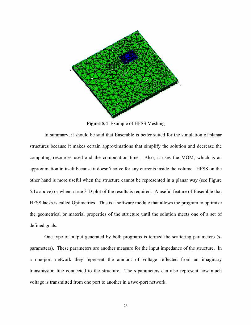
Figure 5.4 Example of HFSS Meshing
In summary, it should be said that Ensemble is better suited for the simulation of planar
structures because it makes certain approximations that simplify the solution and decrease the
computing resources used and the computation time. Also, it uses the MOM, which is an
approximation in itself because it doesn’t solve for any currents inside the volume. HFSS on the
other hand is more useful when the structure cannot be represented in a planar way (see Figure
5.1c above) or when a true 3-D plot of the results is required. A useful feature of Ensemble that
HFSS lacks is called Optimetrics. This is a software module that allows the program to optimize
the geometrical or material properties of the structure until the solution meets one of a set of
defined goals.
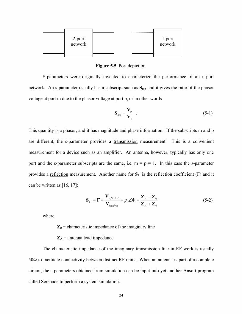
One type of output generated by both programs is termed the scattering parameters (s-
parameters). These parameters are another measure for the input impedance of the structure. In
a one-port network they represent the amount of voltage reflected from an imaginary
transmission line connected to the structure. The s-parameters can also represent how much
voltage is transmitted from one port to another in a two-port network.
24
Figure 5.5 Port depiction.
S-parameters were originally invented to characterize the performance of an n-port
network. An s-parameter usually has a subscript such as Smp and it gives the ratio of the phasor
voltage at port m due to the phasor voltage at port p, or in other words
p
mmp V
VS = . (5-1)
This quantity is a phasor, and it has magnitude and phase information. If the subscripts m and p
are different, the s-parameter provides a transmission measurement. This is a convenient
measurement for a device such as an amplifier. An antenna, however, typically has only one
port and the s-parameter subscripts are the same, i.e. m = p = 1. In this case the s-parameter
provides a reflection measurement. Another name for S11 is the reflection coefficient (Γ) and it
can be written as [16, 17]:
0
011
ZZZZ
VV
ΓS+−
=Φ∠===A
A
incident
reflected ρ (5-2)
where
Z0 = characteristic impedance of the imaginary line
ZA = antenna load impedance
The characteristic impedance of the imaginary transmission line in RF work is usually
50Ω to facilitate connectivity between distinct RF units. When an antenna is part of a complete
circuit, the s-parameters obtained from simulation can be input into yet another Ansoft program
called Serenade to perform a system simulation.
2-port
network
1-port
network
25
5.2. ASITIC
ASITIC is a public domain software package that performs the analysis of passive
devices placed on the silicon substrate [14]. ASITIC is an abbreviation for Analysis and
Simulation of Inductors and Transformers for Integrated Circuits. ASITIC is a program that is
similar to the Ansoft electromagnetic tools in the type of analysis that it performs. However, it
has been optimized for designs specifically on a chip and, therefore, it runs faster. This program
produces s-parameters or it can produce an equivalent circuit composed of inductors, capacitors,
and resistors. The first step in an ASITIC analysis is the creation of Maxwell’s equations to
describe the structure. Then these equations are converted into a matrix using Green’s functions.
The matrix is then solved for the currents on the surface of the structure. The program then uses
the currents to derive the s-parameters and the equivalent circuit model.
6.0 Testing Procedures
6.1 Rig
A fresh-manufactured chip is received from the foundry with a chip surface to which
contacts can be wire bonded. The chip is laid out with special pads to which wire several
microns in diameter will be bonded with a wire-bonding machine. The other side of the wire
will be connected to a solid contact outside the chip. Since we are dealing with high frequencies,
the length of this wire will certainly have an affect on the circuit characteristics. Because of this
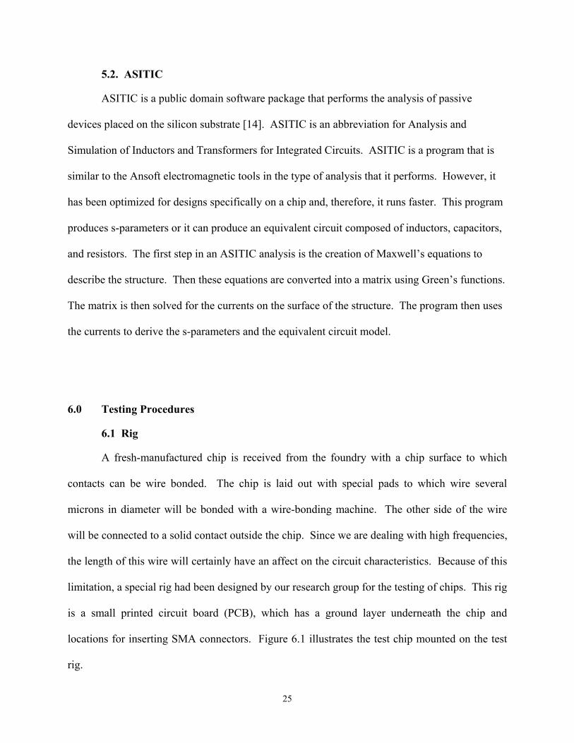
limitation, a special rig had been designed by our research group for the testing of chips. This rig
is a small printed circuit board (PCB), which has a ground layer underneath the chip and
locations for inserting SMA connectors. Figure 6.1 illustrates the test chip mounted on the test
rig.
26
Figure 6.1 Test Rig
6.2 Network Analyzer
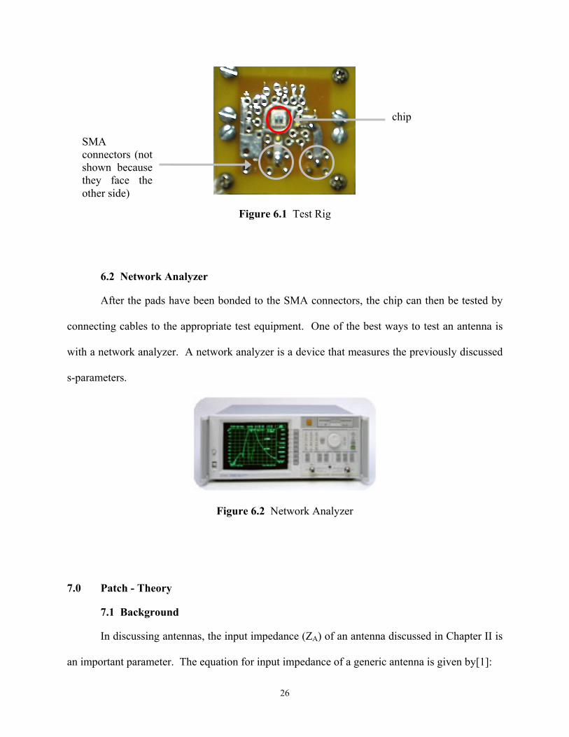
After the pads have been bonded to the SMA connectors, the chip can then be tested by
connecting cables to the appropriate test equipment. One of the best ways to test an antenna is
with a network analyzer. A network analyzer is a device that measures the previously discussed
s-parameters.
Figure 6.2 Network Analyzer
7.0 Patch - Theory
7.1 Background
In discussing antennas, the input impedance (ZA) of an antenna discussed in Chapter II is
an important parameter. The equation for input impedance of a generic antenna is given by[1]:
SMA connectors (not shown because they face the other side)
chip
27
ZA(f)=RA+jXA=(Rr+RL)+j(XA+Xi) (7-1)
The parameters are defined as follows:
Rr: Radiation resistance RL: Loss resistance
XA: Inductive reactance (=ωLA) Xi: Reactance of conductor (=ωLi)
As was mentioned in the Introduction, it is important to minimize the radiation emitted
from the feed. To accomplish this task, many different feeding methods have been developed.
Some of the most common ones are the probe feed, the coupled feed, and the microstrip feed.
The probe feed uses a coaxial probe and is commonly used in circular patches and in rectangular
patches to create circular polarization. The coupled feed is located above or below the patch, and
it transmits energy onto the antenna without physically touching it. This transmission line uses a
substrate different from that used by the patch in order to minimize radiation losses. To simplify
the analysis of the concepts of antenna feeds, this thesis will only discuss the microstrip feed of
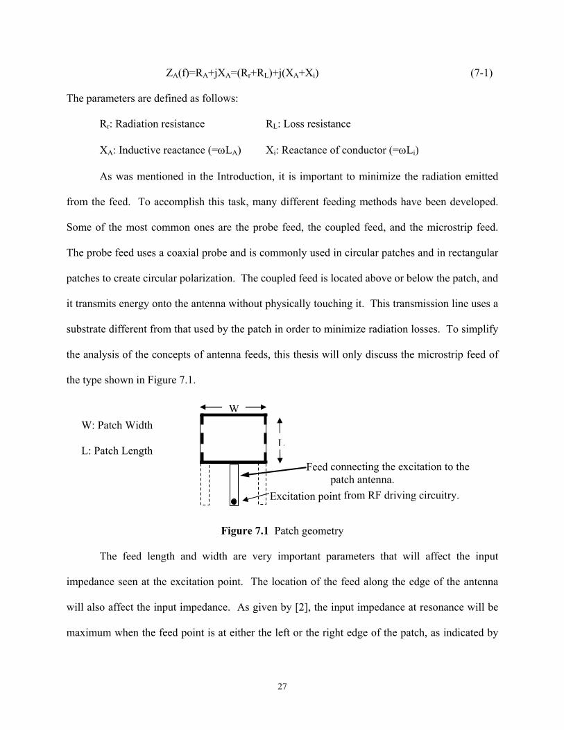
the type shown in Figure 7.1.
Figure 7.1 Patch geometry
The feed length and width are very important parameters that will affect the input
impedance seen at the excitation point. The location of the feed along the edge of the antenna
will also affect the input impedance. As given by [2], the input impedance at resonance will be
maximum when the feed point is at either the left or the right edge of the patch, as indicated by
W
L
Feed
Excitation point
connecting the excitation to the patch antenna.
from RF driving circuitry.
W: Patch Width L: Patch Length

28
the dashed feeds shown in Figure 7.1. If the feed point is in the middle, as shown by the solid
feed in Figure 7.1, the input impedance will be zero. In practice, the feed point will be slightly
offset from the center in order to achieve good impedance matching, i.e., maximum power
transfer.
The two most common models that are utilized for the analysis of a microstrip patch are
the transmission-line and the cavity models. The transmission-line model views the patch
antenna as having two radiating slots separated by a length L, shown by the thick solid lines in
Figure 7.1. The slots that are separated by the width W, shown by the thick dashed lines in the
same figure, are neglected because the radiation components emitted from them cancel each
other out in the far field. The calculation for the admittance of the first radiating slot is the same
as that of the second slot since they have exactly the same dimensions. However, to calculate the
total admittance seen at the input, the admittance of the second slot has to be reflected to the
input. This becomes challenging mathematically, but it can be simplified when the resonant
frequency is reached. At resonance, when λ=2L, the input admittance is given by Balanis as:
YA(f)=2G1 (7-2)
where the conductance is expressed as:
101h 4
2411
120)(
2411
120 0
200
2220
01 <
−=
−=
λεµπ
λhf
cWfhkWG
in which λ0 is the wavelength in free space and h is the height of the dielectric.
As mentioned in [5], the feed itself is a radiator and has an effect on the far field radiation
pattern produced by the antenna. Because of this the antenna radiation pattern is difficult to
control. It is common for half the available power to be lost in the feed. Therefore, a successful
29
feed/antenna design will seek to minimize the radiation of the feed and maximize the radiation of
the antenna at a given frequency.
7.2 Frequency
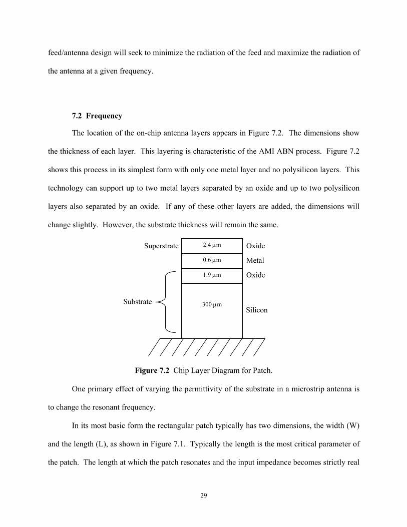
The location of the on-chip antenna layers appears in Figure 7.2. The dimensions show
the thickness of each layer. This layering is characteristic of the AMI ABN process. Figure 7.2
shows this process in its simplest form with only one metal layer and no polysilicon layers. This
technology can support up to two metal layers separated by an oxide and up to two polysilicon
layers also separated by an oxide. If any of these other layers are added, the dimensions will
change slightly. However, the substrate thickness will remain the same.
Figure 7.2 Chip Layer Diagram for Patch.
One primary effect of varying the permittivity of the substrate in a microstrip antenna is
to change the resonant frequency.
In its most basic form the rectangular patch typically has two dimensions, the width (W)
and the length (L), as shown in Figure 7.1. Typically the length is the most critical parameter of
the patch. The length at which the patch resonates and the input impedance becomes strictly real
1.9 µm
300 µm
0.6 µm
Silicon
Oxide
Metal
2.4 µm OxideSuperstrate
Substrate
30
is approximately λ/2. The length will be slightly different from half a wavelength because of
fringing effects which can be accounted for by ∆L given below. When calculating the length, we
pretend that the patch is located in a homogeneous dielectric with an effective dielectric constant
whose equation is given below as well. For a microstrip patch the length is given by the
following formula [1, 18]:
LcLeffr
∆−= 2f2 ,r ε
(7-3)
where
fr is the resonant frequency of the antenna, and εr is the relative permittivity of the dielectric,
1h
W If 1212
12
1 21
, ≥
+
−+
+=
−
Whrr
effrεε
ε (7-3a)
1hW If 104.0121
21
21 2
21
, <
−+
+
−+
+=
−
hW
Whrr
effrεε
ε (7-3b)
)8.0)(258.0(
)264.0)(3.0(412.0
,
,
+−
++=∆
hW
hW
hLeffr
effr
ε
ε (7-3c)
The resonant frequency is that frequency at which the antenna exhibits resonance, and the
impedance of the antenna is strictly real. The resonant frequency may also be called the
resonance frequency or the operating frequency. All these terms mean the same thing and will
be used interchangeably throughout this thesis. With simple algebraic manipulation (7-3) can be
solved for the resonant frequency as a function of permittivity. This yields:
effrr LL
c
,)2(2f
ε∆+= (7-4)

31
The difficulty with this formula is that it is intended for a microstrip patch with only one
dielectric layer. In a patch antenna on a CMOS chip, there exist two dielectric layers between
the patch and the ground. These two layers are the oxide and the silicon. Also, there is a layer of
oxide above the patch that is called the superstrate. The oxide layer is the one that is directly
adjacent to the patch, and the silicon is the one below the oxide. The details of this layering were
shown in Figure 7.2. Simulations of the on-chip spiral have shown that the permittivity of the
oxide layer has an immediate effect on the resonant frequency of the antenna while the
permittivity of the substrate has little or no effect. This result allows us to model the on-chip
antenna as being sandwiched between two oxide layers. With this simplification, a relationship
similar to the one in (7-3) can be established for an on-chip antenna. In order to obtain this
relationship, an expression for the effective relative permittivity of an on-chip antenna has to be
derived.
From (7-4), it is seen that the length correction factor, symbolized by ∆L, has an effect on
the resonant frequency as well. By simple reasoning, from (7-3b), it can be concluded that ∆L
becomes significant at low values of εr,eff, and high values of the substrate height, h. For the
microstrip patch configuration to be discussed in Section 8.B, the calculated value of εr,eff is 8.64
and the value of h is 300x10-6 m. These values prohibit ∆L from being large and, therefore, its
effect on the resonant frequency can be neglected.
The width is a less critical parameter because it has a negligible effect on the resonance
frequency but affects the efficiency of the antenna. It is given by [1]:
.1
2f2 +
=rr
cWε
(7-5)

32
7.3 Bandwidth and Radiating Efficiency
As stated in [5], for a microstrip antenna the operating bandwidth is proportional to the
distance between the antenna and the ground plane. The authors arrive at this conclusion from
analyzing the transmission line model of the microstrip patch antenna. Their results are
summarized by the following formula for the total-Q factor of a microstrip radiator:
BANDWIDTHπf2
)PPh(Pπf2
cdr
rsrTQ =
++=
ξ (7-6)
In the above formula, the parameters important to our analysis are:
h: Substrate height Pr: Power radiated by the antenna
Pd: Power lost to the dielectric Pc: Power lost to the conductor
The formula shows that the bandwidth of a microstrip antenna is proportional to the distance h.
The bandwidth is typically given as 2πfr/QT [20].
Another consequence of this equation is that the losses increase the bandwidth. The
losses however also play a role in another important parameter, the efficiency of the antenna,
given by:
%100PPP
P
cdr
r x++
=η (7-7)
From the two equations presented in this section, it should be clear that there is a trade-off that
must be made between the bandwidth and efficiency of the antenna.
In order to estimate the effect of the substrate permittivity on the bandwidth, (7-4) can be
substituted into (7-6). This results in:
hPπ2
)2(2)PPh(Pπf2
,cdr
s
effr
srT LL
cQ ξε
ξ∆+
=++
= (7-8)
33
Thus,
BANDWIDTH = 2πfr/QT ∝ √εr,eff (7-9)
In the above relationship, the sum of the three power components is assumed to be constant and
can be combined into the total power P. As can be seen from (7-9), the antenna bandwidth is
directly proportional to the square root of the effective relative permittivity. In order to apply
(7-8) to on-chip antennas, the expression for the effective relative permittivity will have to be
modified as discussed in the previous section.
8.0 Patch – Simulations
8.1 Introduction
As was shown in Figure 1.4, the patch geometry is different from that of the typical
microstrip on a printed circuit board. Since the majority of research done on planar antennas has
been aimed towards the microstrip, there is currently very little design information available for
IC antennas. Therefore, the first step in the simulation is to observe through simulation what
effects the differences in IC and microstrip configurations have on the antenna performance.
After that is known, the permittivities of the oxide layers will be modified and the effects on the
antenna performance will be studied.
The simulations will begin with a microstrip patch antenna designed using the equations
given in Section 7. These simulations will be done in Ansoft HFSS in order to display the 3D
radiation patterns and get a measure of efficiency. The substrate used for this antenna will be
intrinsic silicon. The input impedance curve for the antenna as a function of frequency will be
plotted and it will be used to determine those frequencies where the antenna resonates. This will
34
be the departure point for the rest of the analysis of the rectangular patch. Following the
comparison of the design results with the simulation, the substrate will be doped, and one by one
the oxide layers will be added to transform the microstrip structure into one on-the-chip. At
every point, the effects of each modification will be noted and discussed. The goal will be to
observe if in the process of the transformation a low operating frequency can be found.
After the chip structure is complete, the permittivity of each of the oxides will be varied
while the other oxide’s permittivity is kept constant. The effects of the permittivity variations on
the resonant frequency will be noted. The goal of these experiments will be to note what can be
done to lower the operating frequency of the patch.
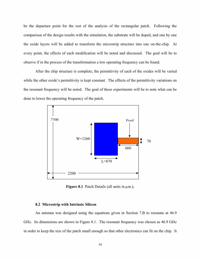
Figure 8.1 Patch Details (all units in µm.).
8.2 Microstrip with Intrinsic Silicon
An antenna was designed using the equations given in Section 7.B to resonate at 46.9
GHz. Its dimensions are shown in Figure 8.1. The resonant frequency was chosen as 46.9 GHz
in order to keep the size of the patch small enough so that other electronics can fit on the chip. It
70
L=870
660
2200
2200 Feed
W=1260
35
would also provide an antenna that would not require a much larger and more expensive chip.
The substrate used in the design was 300 µm. thick undoped silicon, fixed by the available
CMOS process, to preserve the same dimensions as the complete CMOS chip. The ground plane
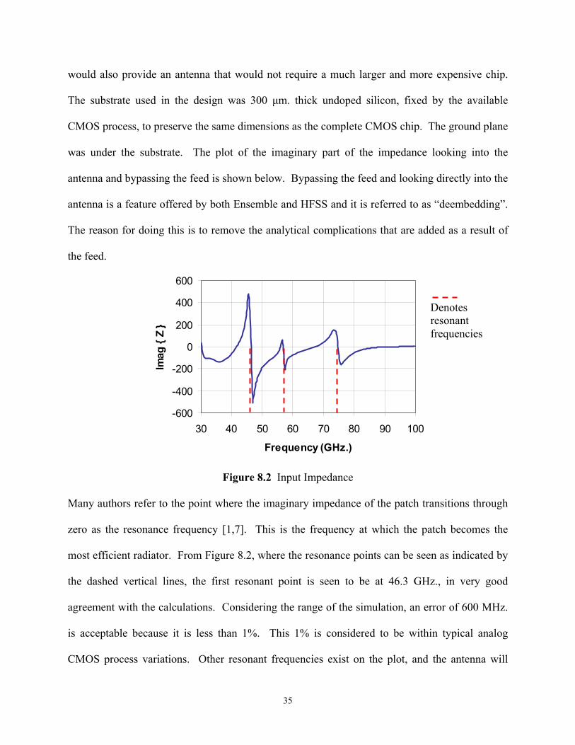
was under the substrate. The plot of the imaginary part of the impedance looking into the
antenna and bypassing the feed is shown below. Bypassing the feed and looking directly into the
antenna is a feature offered by both Ensemble and HFSS and it is referred to as “deembedding”.
The reason for doing this is to remove the analytical complications that are added as a result of
the feed.
-600
-400
-200
0
200
400
600
30 40 50 60 70 80 90 100
Frequency (GHz.)
Imag
Z
Figure 8.2 Input Impedance
Many authors refer to the point where the imaginary impedance of the patch transitions through
zero as the resonance frequency [1,7]. This is the frequency at which the patch becomes the
most efficient radiator. From Figure 8.2, where the resonance points can be seen as indicated by
the dashed vertical lines, the first resonant point is seen to be at 46.3 GHz., in very good
agreement with the calculations. Considering the range of the simulation, an error of 600 MHz.
is acceptable because it is less than 1%. This 1% is considered to be within typical analog
CMOS process variations. Other resonant frequencies exist on the plot, and the antenna will
Denotes resonant frequencies
36
work at those frequencies as well. However, the design equations are for the dominant mode at
46.9 GHz., which achieves the best performance.
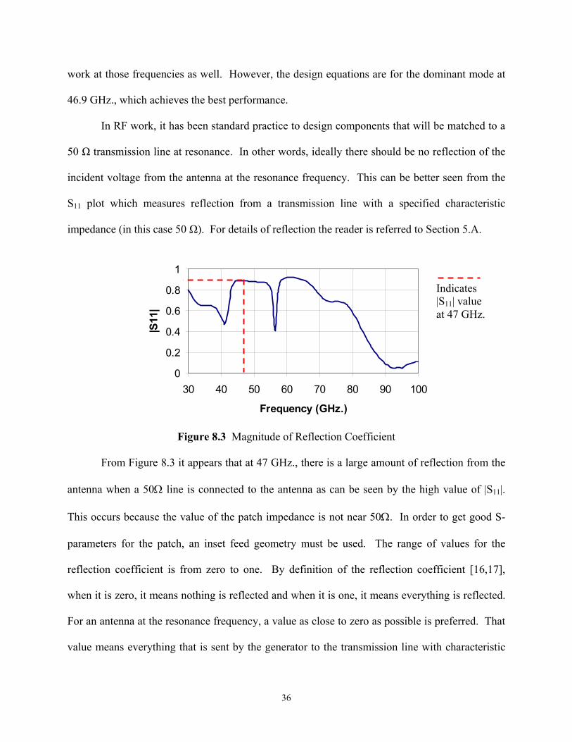
In RF work, it has been standard practice to design components that will be matched to a
50 Ω transmission line at resonance. In other words, ideally there should be no reflection of the
incident voltage from the antenna at the resonance frequency. This can be better seen from the
S11 plot which measures reflection from a transmission line with a specified characteristic
impedance (in this case 50 Ω). For details of reflection the reader is referred to Section 5.A.
0
0.2
0.4
0.6
0.8
1
30 40 50 60 70 80 90 100
Frequency (GHz.)
|S11
|
Figure 8.3 Magnitude of Reflection Coefficient
From Figure 8.3 it appears that at 47 GHz., there is a large amount of reflection from the
antenna when a 50Ω line is connected to the antenna as can be seen by the high value of |S11|.
This occurs because the value of the patch impedance is not near 50Ω. In order to get good S-
parameters for the patch, an inset feed geometry must be used. The range of values for the
reflection coefficient is from zero to one. By definition of the reflection coefficient [16,17],
when it is zero, it means nothing is reflected and when it is one, it means everything is reflected.
For an antenna at the resonance frequency, a value as close to zero as possible is preferred. That
value means everything that is sent by the generator to the transmission line with characteristic
Indicates |S11| value at 47 GHz.
37
impedance Z0 is transmitted to the load, which is the antenna. This occurs because of the
following relationship: Reflection Coefficient = 1 – Transmission Coefficient. When the antenna
is used in the receiving mode, the situation is identical, but now the antenna serves as the
generator whose impedance must be matched to the transmission line to minimize reflection.
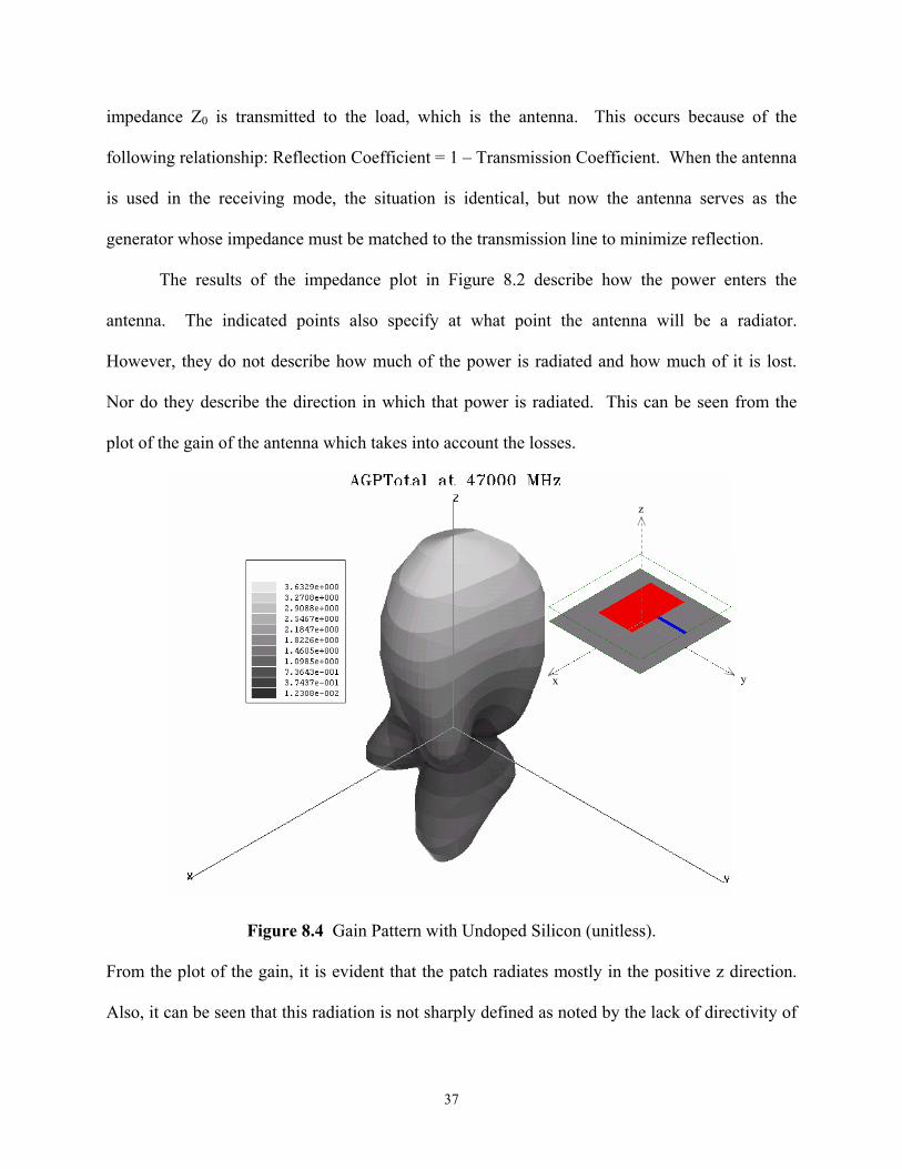
The results of the impedance plot in Figure 8.2 describe how the power enters the
antenna. The indicated points also specify at what point the antenna will be a radiator.
However, they do not describe how much of the power is radiated and how much of it is lost.
Nor do they describe the direction in which that power is radiated. This can be seen from the
plot of the gain of the antenna which takes into account the losses.
Figure 8.4 Gain Pattern with Undoped Silicon (unitless).
From the plot of the gain, it is evident that the patch radiates mostly in the positive z direction.
Also, it can be seen that this radiation is not sharply defined as noted by the lack of directivity of
z
x y
38
the above plot. Directivity is a little better in the negative z direction (down) but little power is
radiated.
As discussed in the section on Antenna Fundamentals, gain is a measure of the power
radiated in a certain direction relative to the power that would be radiated in that same direction
by a lossless isotropic source. In Figure 8.4 above, regions whose gain is greater than one radiate
more power than a lossless isotropic source and those where the gain is less than one radiate less.
The gain can be seen from the color key code in Figure 8.4. In general, gain can be expressed as:
gain (x,y,z) = efficiency • directivity (x,y,z). It follows that gain is a lumped measurement of
efficiency and directivity. From a plot of gain, it is impossible to determine the efficiency
without looking at a corresponding plot of directivity. This is remedied by HFSS, which
provides a separate computation of the antenna efficiency. For this antenna, the computed
efficiency is 95%.
8.3 Microstrip with Doped Silicon
The previous simulation has been performed for silicon that is undoped. The effects of
doping on conductivity were summarized in (4-1) which is repeated here:
σ = qnµn+ qpµp (8-1)
39
-600
-400
-200
0
200
400
600
30 40 50 60 70 80 90 100
Frequency (GHz.)
Imag
Z
Denotes resonant frequencies
-70-60-50-40-30-20-10
01020
30 40 50 60 70 80 90 100
Frequency (GHz.)
Imag
Z
a. Silicon with Doping b. Silicon without Doping
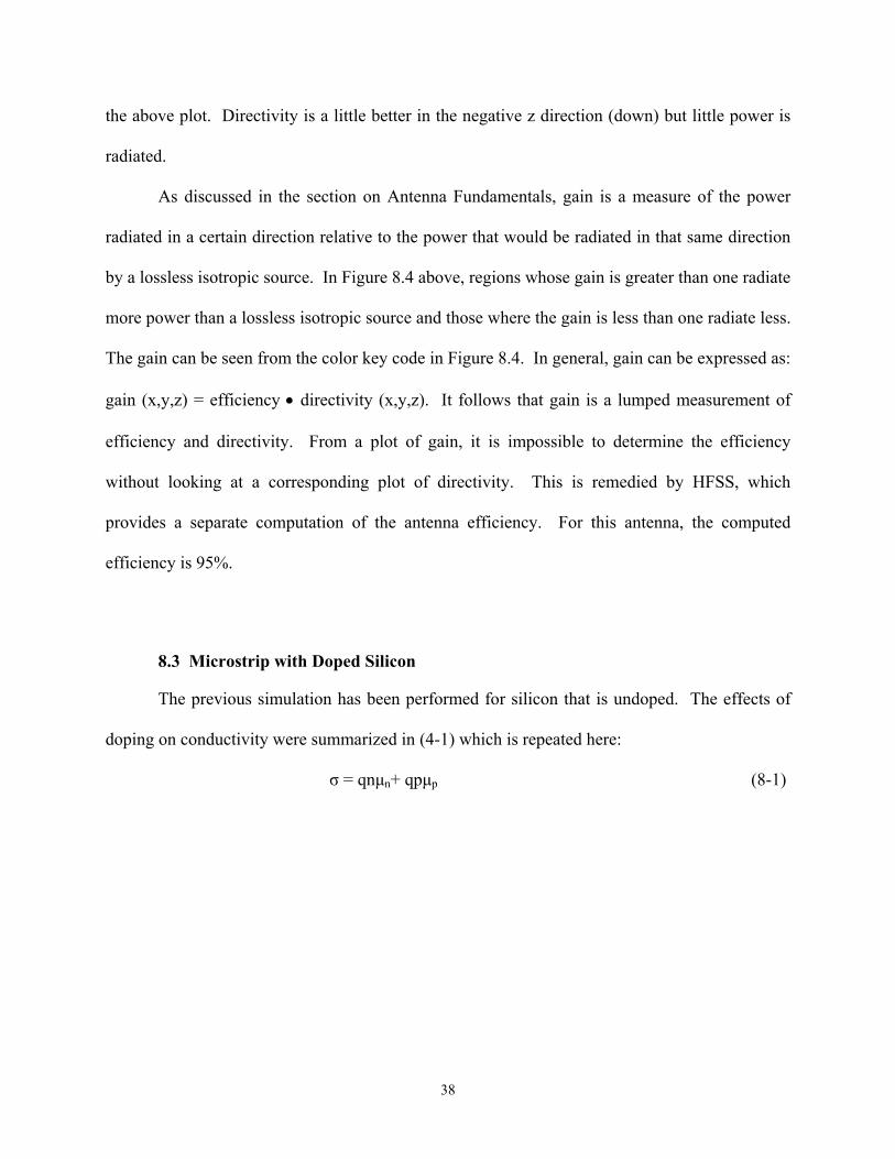
Figure 8.5 Input Impedance with and without Doping
The results of the simulation that account for the non-zero conductivity, which occurs as a result
of doping, are plotted in Figure 8.5. A close-up view of the point in Figure 8.5a, where the
impedance crosses the zero line will reveal that the frequency at which this phenomenon occurs
is 44.1 GHz. Therefore, one effect of the doping is to decrease the resonant frequency. Another
effect is to eliminate all the non-dominant modes at which resonance also occurs. In this
example, the doping is relatively light [1016 atoms/cm3], and a heavier doping [1018 atoms/cm3]
is likely to have an even greater effect. The effects of doping also appear in the radiating
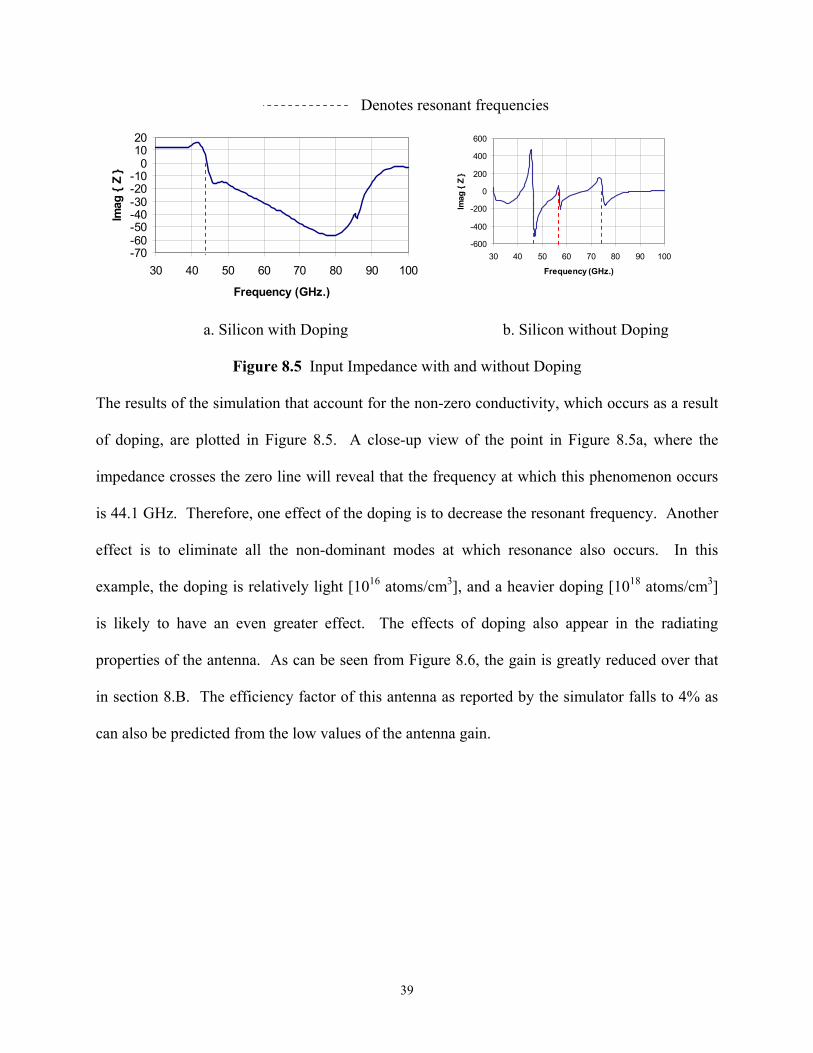
properties of the antenna. As can be seen from Figure 8.6, the gain is greatly reduced over that
in section 8.B. The efficiency factor of this antenna as reported by the simulator falls to 4% as
can also be predicted from the low values of the antenna gain.
40
Figure 8.6 Gain Pattern with Doped Silicon (unitless).
From this simulation, two generalizations can be inferred. The advantage gained by
controlling the doping level of the substrate is the ability to control the resonant frequency,
subject to the limitations described below. Undoped silicon is lossless because its conductivity is
close to zero. Doping increases the conductivity of the silicon and it becomes lossy. Typically,
the doping levels range from 1016 atoms/cm3, which is considered low-doping, to 1020
atoms/cm3, which is considered very high doping. Thus, the ability to control the resonant
frequency by doping will be limited by the level of the doping. It will also be limited by the
efficiency drop that occurs in the antenna because of the doping, as was demonstrated in this
subsection. The main reason for these effects is the modification of the crystalline structure of
pure silicon that occurs as a result of doping.
z
x y
41
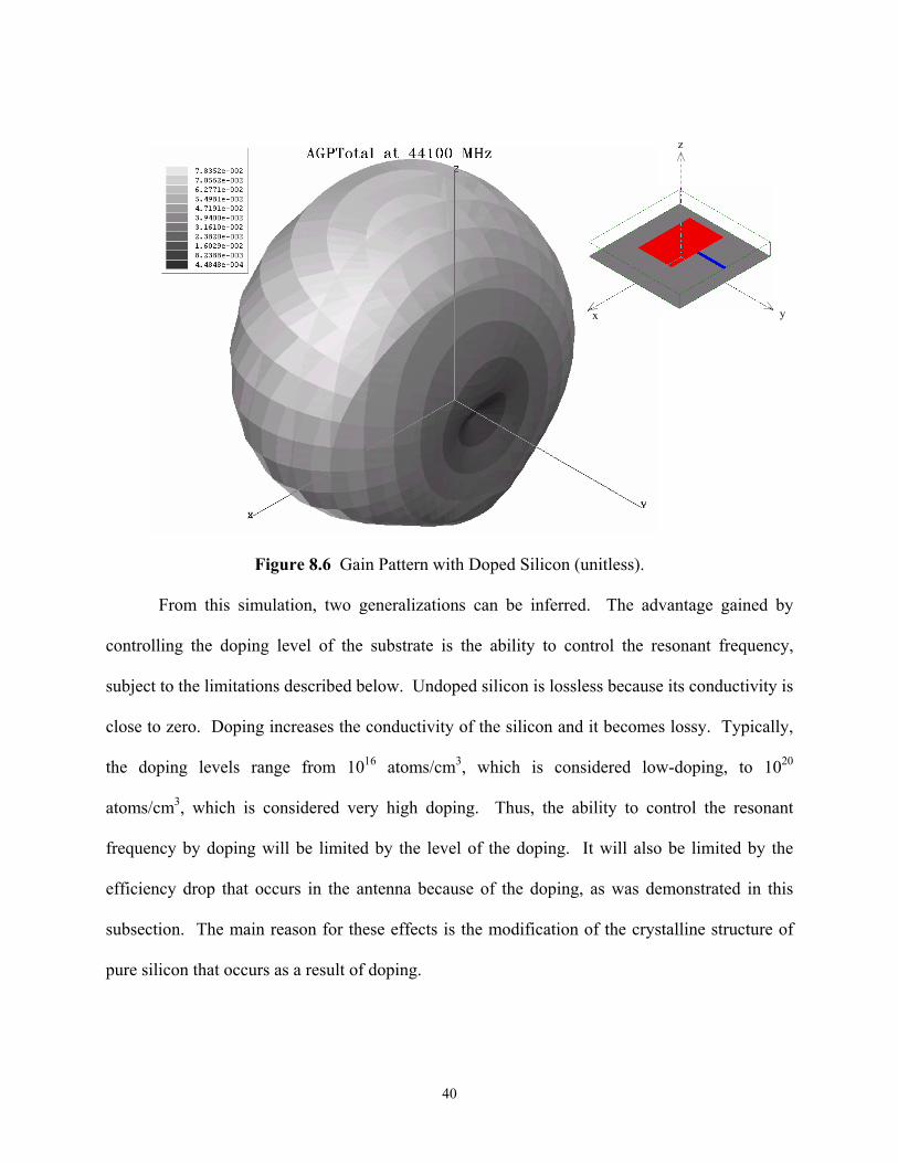
8.4 Microstrip with Substrate Oxide and Doped Silicon
The progression from the microstrip to the chip where the different layers are added is
continued in this section with the insertion of the oxide layer between the metal and silicon.
According to the information published in literature, it is assumed that the oxide is undoped [20].
Because of this, its conductivity is assumed to be zero. The configuration of layers at this stage
will be as shown in Figure 8.7 below. By simulating this configuration, it will be possible to
understand what effect the addition of the substrate oxide layer has on the resonance frequency
of the antenna. Understanding this effect will enable the modification of the equation for the
effective relative permittivity of an antenna with a multi-layer dielectric configuration. The
consequences of the addition of the superstrate oxide layer will be described in the next
subsection.
Figure 8.7 Geometry for Simulation
1.9 µm
300 µm
0.6 µm
Silicon
Oxide
Metal
Substrate
42
-80-70-60-50-40-30-20-10
0
30 40 50 60 70 80 90 100
Frequency (GHz.)
Imag
Z
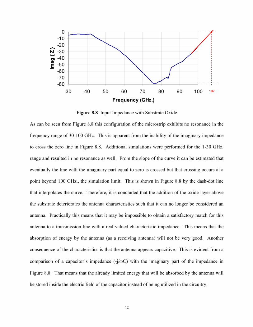
Figure 8.8 Input Impedance with Substrate Oxide
As can be seen from Figure 8.8 this configuration of the microstrip exhibits no resonance in the
frequency range of 30-100 GHz. This is apparent from the inability of the imaginary impedance
to cross the zero line in Figure 8.8. Additional simulations were performed for the 1-30 GHz.
range and resulted in no resonance as well. From the slope of the curve it can be estimated that
eventually the line with the imaginary part equal to zero is crossed but that crossing occurs at a
point beyond 100 GHz., the simulation limit. This is shown in Figure 8.8 by the dash-dot line
that interpolates the curve. Therefore, it is concluded that the addition of the oxide layer above
the substrate deteriorates the antenna characteristics such that it can no longer be considered an
antenna. Practically this means that it may be impossible to obtain a satisfactory match for this
antenna to a transmission line with a real-valued characteristic impedance. This means that the
absorption of energy by the antenna (as a receiving antenna) will not be very good. Another
consequence of the characteristics is that the antenna appears capacitive. This is evident from a
comparison of a capacitor’s impedance (-j/ωC) with the imaginary part of the impedance in
Figure 8.8. That means that the already limited energy that will be absorbed by the antenna will
be stored inside the electric field of the capacitor instead of being utilized in the circuitry.
107

43
8.5 Chip with Sub and Superstrates and Doped Silicon
At this point the superstrate layer is added to the configuration to transform the microstrip
structure to one on the chip. The layer configuration is shown below in Figure 8.9.
Figure 8.9 Geometry for Simulation
The simulation results again show that the antenna does not resonate in the simulation
range, but that the resonance point appears to be not too far beyond the 100 GHz. The range
above 100 GHz. was not included in the simulation because of the associated time constraints.
Each simulation reported here took an average time of 30 minutes. According to the author’s
experience, if the range had been increased to 500 GHz., the simulation time would have
increased by a factor of five, to two and a half hours. Because of the absence of software
features that automate the simulations, simulating such a large range would be impractical.
Superstrate
Substrate
1.9 µm
0.6 µm
Silicon
Oxide
Metal 1
2.4 µm Oxide
300 µm
44
-350-300-250-200-150-100-50
050
30 40 50 60 70 80 90 100
Frequency (GHz.)
Impe
danc
e (O
hms)
Imag Z Real Z
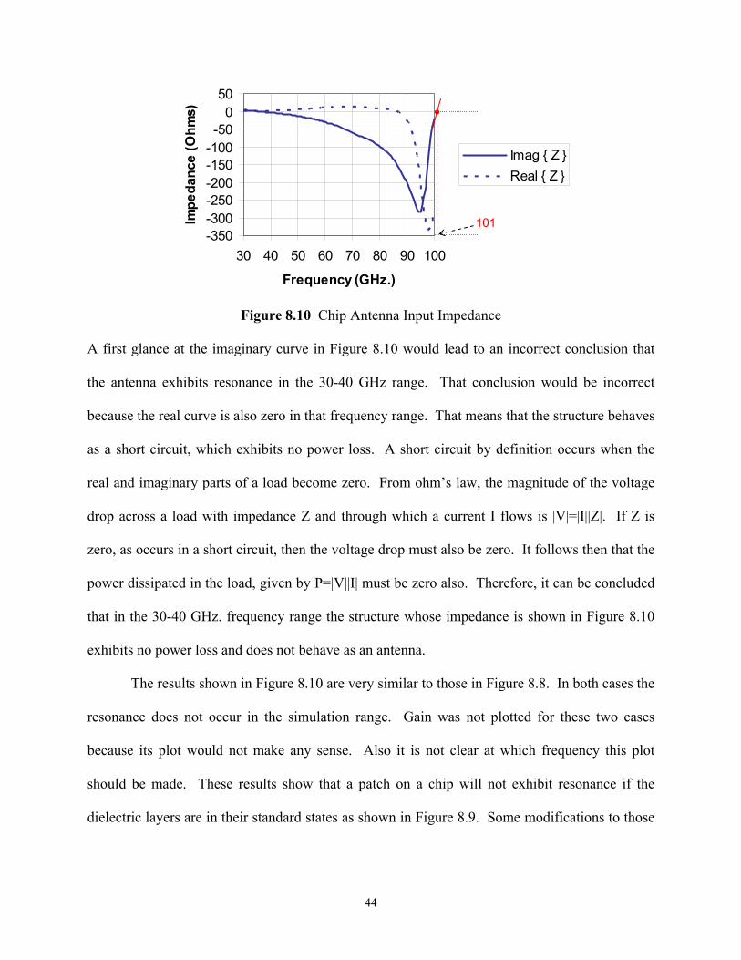
Figure 8.10 Chip Antenna Input Impedance
A first glance at the imaginary curve in Figure 8.10 would lead to an incorrect conclusion that
the antenna exhibits resonance in the 30-40 GHz range. That conclusion would be incorrect
because the real curve is also zero in that frequency range. That means that the structure behaves
as a short circuit, which exhibits no power loss. A short circuit by definition occurs when the
real and imaginary parts of a load become zero. From ohm’s law, the magnitude of the voltage
drop across a load with impedance Z and through which a current I flows is |V|=|I||Z|. If Z is
zero, as occurs in a short circuit, then the voltage drop must also be zero. It follows then that the
power dissipated in the load, given by P=|V||I| must be zero also. Therefore, it can be concluded
that in the 30-40 GHz. frequency range the structure whose impedance is shown in Figure 8.10
exhibits no power loss and does not behave as an antenna.
The results shown in Figure 8.10 are very similar to those in Figure 8.8. In both cases the
resonance does not occur in the simulation range. Gain was not plotted for these two cases
because its plot would not make any sense. Also it is not clear at which frequency this plot
should be made. These results show that a patch on a chip will not exhibit resonance if the
dielectric layers are in their standard states as shown in Figure 8.9. Some modifications to those
101
45
layers must be made in order to have an antenna that will resonate in the 30-100 GHz. frequency
range.
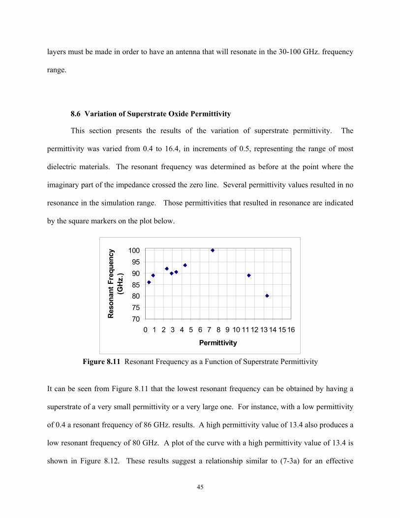
8.6 Variation of Superstrate Oxide Permittivity
This section presents the results of the variation of superstrate permittivity. The
permittivity was varied from 0.4 to 16.4, in increments of 0.5, representing the range of most
dielectric materials. The resonant frequency was determined as before at the point where the
imaginary part of the impedance crossed the zero line. Several permittivity values resulted in no
resonance in the simulation range. Those permittivities that resulted in resonance are indicated
by the square markers on the plot below.
707580859095
100
0 1 2 3 4 5 6 7 8 9 10 11 12 13 14 15 16
Permittivity
Reso
nant
Fre
quen
cy
(GHz
.)
Figure 8.11 Resonant Frequency as a Function of Superstrate Permittivity
It can be seen from Figure 8.11 that the lowest resonant frequency can be obtained by having a
superstrate of a very small permittivity or a very large one. For instance, with a low permittivity
of 0.4 a resonant frequency of 86 GHz. results. A high permittivity value of 13.4 also produces a
low resonant frequency of 80 GHz. A plot of the curve with a high permittivity value of 13.4 is
shown in Figure 8.12. These results suggest a relationship similar to (7-3a) for an effective
46
relative permittivity, and it is not a linear relationship. In other words, from the results it appears
that the dependence of the effective relative permittivity on the relative permittivity of the
superstrate is not linear.
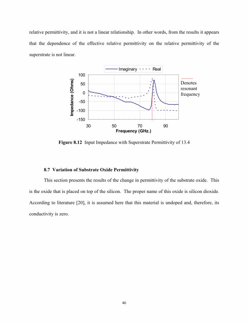
-150
-100
-50
0
50
100
30 50 70 90Frequency (GHz.)
Impe
danc
e (O
hms)
Imaginary Real
Figure 8.12 Input Impedance with Superstrate Permittivity of 13.4
8.7 Variation of Substrate Oxide Permittivity
This section presents the results of the change in permittivity of the substrate oxide. This
is the oxide that is placed on top of the silicon. The proper name of this oxide is silicon dioxide.
According to literature [20], it is assumed here that this material is undoped and, therefore, its
conductivity is zero.
Denotes resonant frequency
47
92
94
96
98
100
102
0 2 4 6 8
Permittivity
Reso
nant
Fre
quen
cy
(GHz
.)
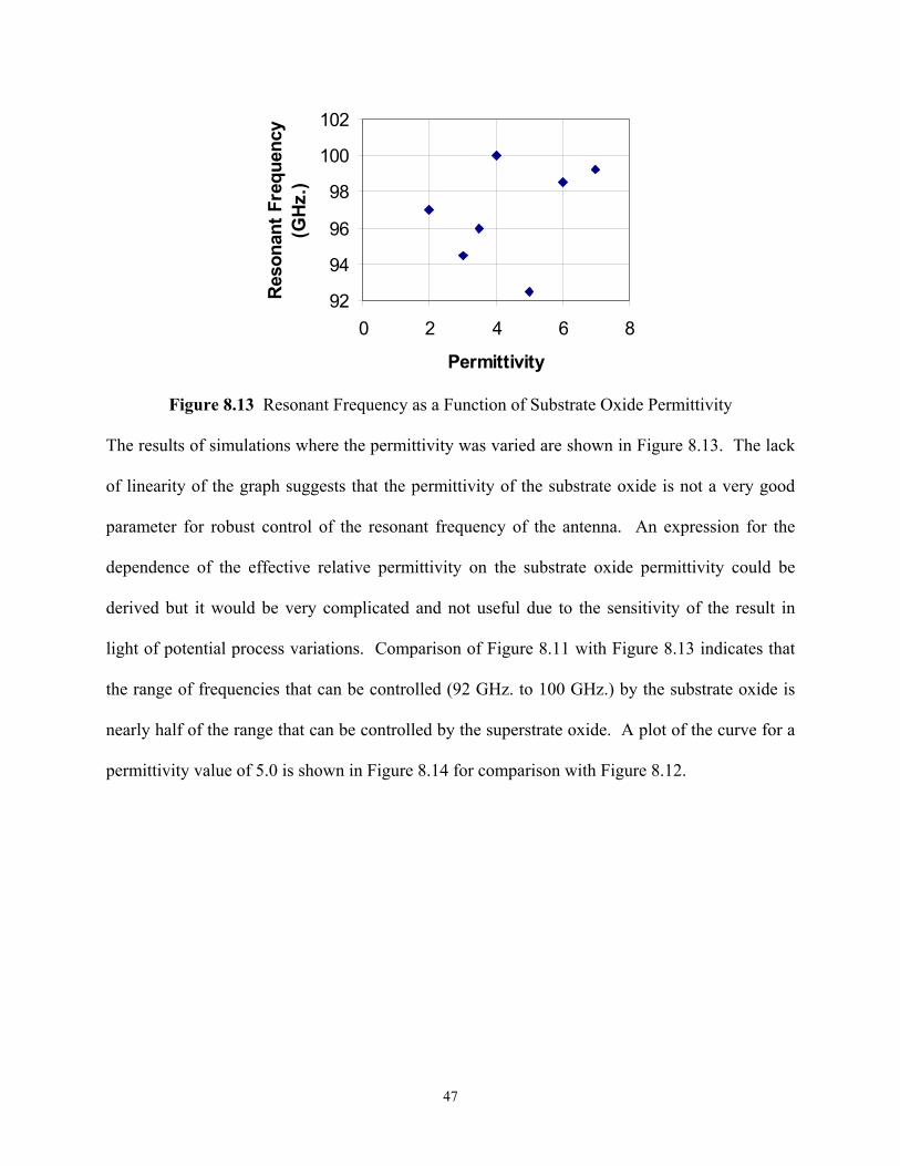
Figure 8.13 Resonant Frequency as a Function of Substrate Oxide Permittivity
The results of simulations where the permittivity was varied are shown in Figure 8.13. The lack
of linearity of the graph suggests that the permittivity of the substrate oxide is not a very good
parameter for robust control of the resonant frequency of the antenna. An expression for the
dependence of the effective relative permittivity on the substrate oxide permittivity could be
derived but it would be very complicated and not useful due to the sensitivity of the result in
light of potential process variations. Comparison of Figure 8.11 with Figure 8.13 indicates that
the range of frequencies that can be controlled (92 GHz. to 100 GHz.) by the substrate oxide is
nearly half of the range that can be controlled by the superstrate oxide. A plot of the curve for a
permittivity value of 5.0 is shown in Figure 8.14 for comparison with Figure 8.12.

48
-200
-150
-100
-50
0
50
30 50 70 90Frequency (GHz.)
Impe
danc
e (O
hms)
Imaginary Real
Figure 8.14 Input Impedance with Substrate Permittivity of 5.0
9.0 Square Spiral – Simulations
9.1 Introduction
Another type of on-chip antenna, designed to operate in a lower frequency range than the
patch, was investigated next. This antenna had been designed previously using the software tool
ASITIC [14] discussed elsewhere. It is a single-turn [14] square spiral designed with a goal to
resonate in the 1-1000 MHz. range. Just as in the patch case, resonance is achieved when the
imaginary part of the input impedance approaches zero and the real part is maximum.
Denotes resonant frequency
49
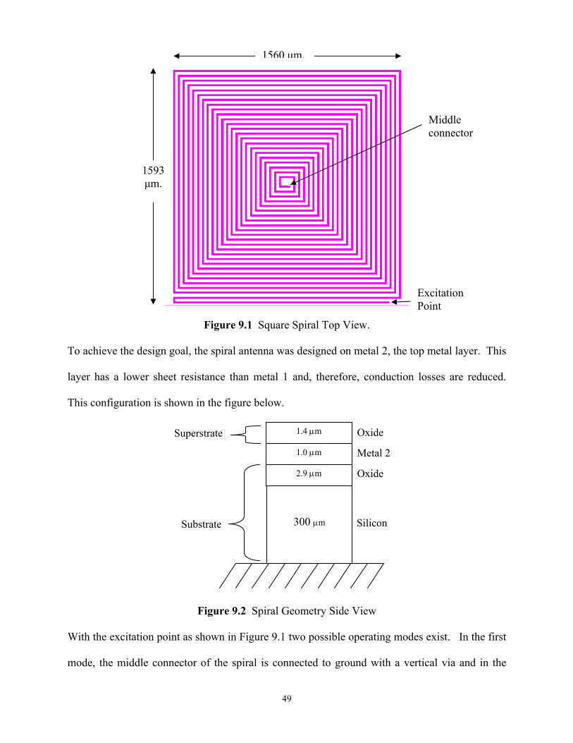
Figure 9.1 Square Spiral Top View.
To achieve the design goal, the spiral antenna was designed on metal 2, the top metal layer. This
layer has a lower sheet resistance than metal 1 and, therefore, conduction losses are reduced.
This configuration is shown in the figure below.
Figure 9.2 Spiral Geometry Side View
With the excitation point as shown in Figure 9.1 two possible operating modes exist. In the first
mode, the middle connector of the spiral is connected to ground with a vertical via and in the
Superstrate
Substrate
2.9 µm
1.0 µm
Silicon
Oxide
Metal 2
1.4 µm Oxide
300 µm
Excitation Point
1593 µm.
1560 µm.
Middle connector
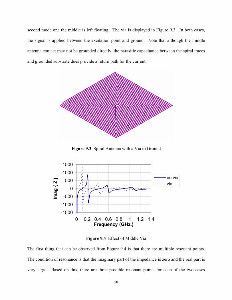
50
second mode one the middle is left floating. The via is displayed in Figure 9.3. In both cases,
the signal is applied between the excitation point and ground. Note that although the middle
antenna contact may not be grounded directly, the parasitic capacitance between the spiral traces
and grounded substrate does provide a return path for the current.
Figure 9.3 Spiral Antenna with a Via to Ground
-1500-1000-500
0500
10001500
0 0.2 0.4 0.6 0.8 1 1.2 1.4Frequency (GHz.)
Imag
Z
no viavia
Figure 9.4 Effect of Middle Via
The first thing that can be observed from Figure 9.4 is that there are multiple resonant points.
The condition of resonance is that the imaginary part of the impedance is zero and the real part is
very large. Based on this, there are three possible resonant points for each of the two cases
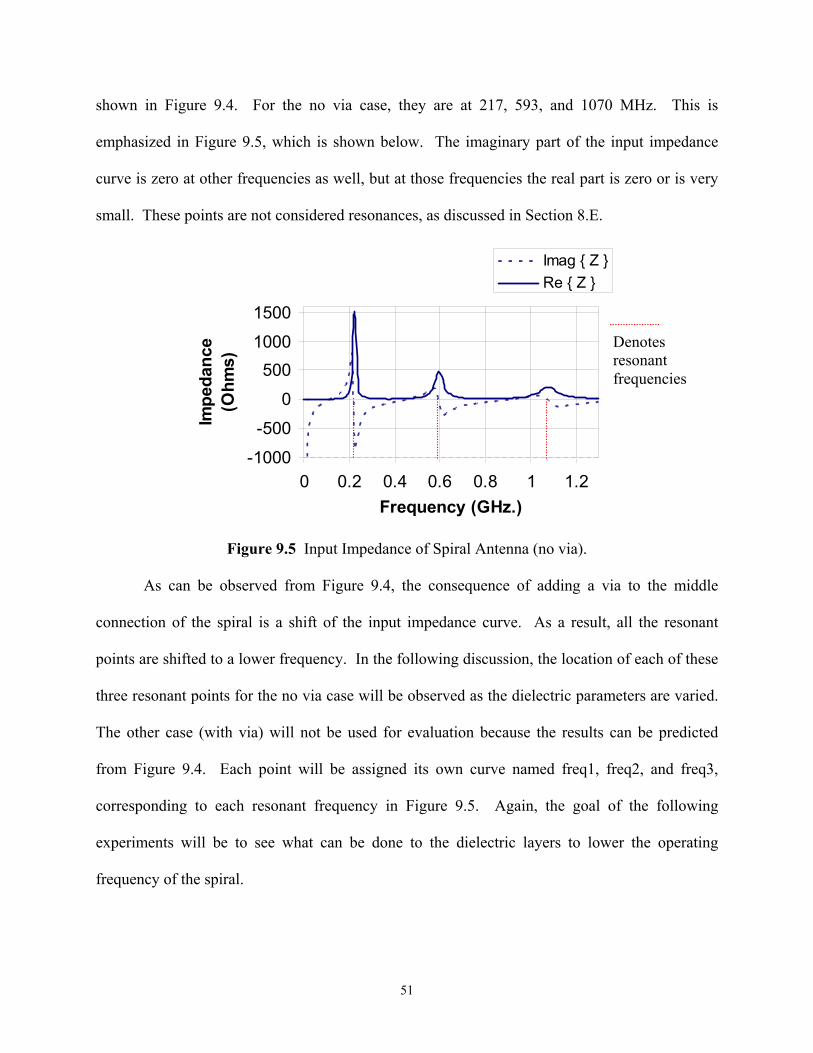
51
shown in Figure 9.4. For the no via case, they are at 217, 593, and 1070 MHz. This is
emphasized in Figure 9.5, which is shown below. The imaginary part of the input impedance
curve is zero at other frequencies as well, but at those frequencies the real part is zero or is very
small. These points are not considered resonances, as discussed in Section 8.E.
Delta 1 (no via)
-1000
-5000
50010001500
0 0.2 0.4 0.6 0.8 1 1.2Frequency (GHz.)
Impe
danc
e (O
hms)
Imag Z Re Z
Figure 9.5 Input Impedance of Spiral Antenna (no via).
As can be observed from Figure 9.4, the consequence of adding a via to the middle
connection of the spiral is a shift of the input impedance curve. As a result, all the resonant
points are shifted to a lower frequency. In the following discussion, the location of each of these
three resonant points for the no via case will be observed as the dielectric parameters are varied.
The other case (with via) will not be used for evaluation because the results can be predicted
from Figure 9.4. Each point will be assigned its own curve named freq1, freq2, and freq3,
corresponding to each resonant frequency in Figure 9.5. Again, the goal of the following
experiments will be to see what can be done to the dielectric layers to lower the operating
frequency of the spiral.
Denotes resonant frequencies
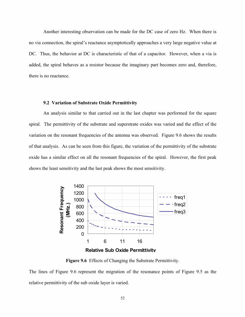
52
Another interesting observation can be made for the DC case of zero Hz. When there is
no via connection, the spiral’s reactance asymptotically approaches a very large negative value at
DC. Thus, the behavior at DC is characteristic of that of a capacitor. However, when a via is
added, the spiral behaves as a resistor because the imaginary part becomes zero and, therefore,
there is no reactance.
9.2 Variation of Substrate Oxide Permittivity
An analysis similar to that carried out in the last chapter was performed for the square
spiral. The permittivity of the substrate and superstrate oxides was varied and the effect of the
variation on the resonant frequencies of the antenna was observed. Figure 9.6 shows the results
of that analysis. As can be seen from this figure, the variation of the permittivity of the substrate
oxide has a similar effect on all the resonant frequencies of the spiral. However, the first peak
shows the least sensitivity and the last peak shows the most sensitivity.
0200400600800
100012001400
1 6 11 16
Relative Sub Oxide Permittivity
Reso
nant
Fre
quen
cy
(MHz
.)
freq1freq2freq3
Figure 9.6 Effects of Changing the Substrate Permittivity.
The lines of Figure 9.6 represent the migration of the resonance points of Figure 9.5 as the
relative permittivity of the sub oxide layer is varied.
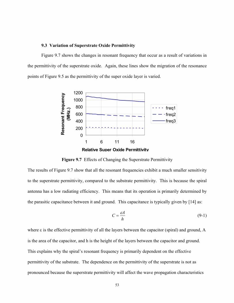
53
9.3 Variation of Superstrate Oxide Permittivity
Figure 9.7 shows the changes in resonant frequency that occur as a result of variations in
the permittivity of the superstrate oxide. Again, these lines show the migration of the resonance
points of Figure 9.5 as the permittivity of the super oxide layer is varied.
0200400600800
10001200
1 6 11 16
Relative Super Oxide Permittivity
Reso
nant
Fre
quen
cy
(MHz
.) freq1freq2freq3
Figure 9.7 Effects of Changing the Superstrate Permittivity
The results of Figure 9.7 show that all the resonant frequencies exhibit a much smaller sensitivity
to the superstrate permittivity, compared to the substrate permittivity. This is because the spiral
antenna has a low radiating efficiency. This means that its operation is primarily determined by
the parasitic capacitance between it and ground. This capacitance is typically given by [14] as:
hAC ε
= (9-1)
where ε is the effective permittivity of all the layers between the capacitor (spiral) and ground, A
is the area of the capacitor, and h is the height of the layers between the capacitor and ground.
This explains why the spiral’s resonant frequency is primarily dependent on the effective
permittivity of the substrate. The dependence on the permittivity of the superstrate is not as
pronounced because the superstrate permittivity will affect the wave propagation characteristics
54
such as its frequency, but it won’t affect the operation of the antenna. Also, both Figure 9.6 and
Figure 9.7 demonstrate that the third frequency has the largest sensitivity of the three.
A comparison of Figures 9.6 and 9.7 leads to the conclusion that the permittivity of the
substrate oxide plays a greater role than the permittivity of the superstrate oxide in determining
the resonant frequency of the spiral. This can be useful to the designer in determining in which
layer the permittivity must be adjusted in order to reach a design goal of a certain resonant
frequency.
10.0 Summary and Conclusions
Design data for the rectangular patch has been presented and analyzed. The design
approach was to present the equations for the microstrip and then show how to adapt those
equations for the case of the on-chip patch. The dependence of the patch resonant frequency on
the antenna’s dimensions and on the effective relative permittivity was shown. The major
modification that must be made to the equations is to calculate the effective relative permittivity
for the antenna on a chip. This is a straightforward calculation for the microstrip antenna, but it
is a much more involved calculation for an antenna on a chip. Based on the results of this thesis,
future research needs to be performed to establish a tractable mathematical relationship.
Following the design information, simulations of the rectangular patch were performed.
The simulations had several goals. The first goal was to show the effect of adding each layer as
the microstrip antenna was transformed into one on a chip. This effect was to decrease the
antenna’s efficiency, reduce the number of resonant frequencies, and some cases resulted in the
disappearance of resonant frequencies from the simulation range. The second goal was to
demonstrate what happens to the antenna’s operating frequency as the relative permittivity of
55
some dielectric layers is varied. This effect was great enough to have a significant impact on the
operating frequency.
The initial microstrip case with the patch placed on top of an undoped silicon substrate
showed very good agreement with the calculated resonance point of 47 GHz. and also very high
radiation efficiency. This suggested that the simulation setup in the software was correct and
validated the setup for the experiments to follow, for which calculated values were not available.
This configuration also resulted in the presence of a multitude of other resonance frequencies,
due to the lossless ness of the silicon substrate. As the conductivity of silicon was modified to
account for the practical scenario of doping, the multiple resonance points were no longer
observed and the 47 GHz. point was shifted to 44.1 GHz. This configuration also resulted in an
attendant severe decrease of the efficiency of the antenna. Subsequent additions of the substrate
and superstrate oxides altered the characteristics of the patch antenna to a very high degree such
that it could no longer be considered an antenna in the 30-100 GHz. simulation range.
At this point, the patch was configured with all the layers that exist on the chip and it
exhibited no resonance. Using the results of the simulation, it was shown that the resonance
frequency could be controlled to a limited degree by varying the superstrate permittivity. Values
in the low (0-3) and high (10-14) ranges of the permittivity had the greatest impact on the
frequency of operation. The maximum shift of 20 GHz. was achieved for a permittivity of 13.4.
Variation of the substrate permittivity also resulted in changes to the frequency of operation, but
those changes were not as predictable and the range of frequencies was decreased. Similar
research done by Jackson and Alexopoulos [4] suggests that it may be possible to affect the
resonant frequency by simultaneously changing the permittivities of the substrate and superstrate
56
of certain geometries. This type of analysis was not considered here and future investigation in
this direction may also be performed.
To illustrate the effects of the permittivity changes on an antenna designed to work at
lower frequencies, a (nearly) square IC spiral was considered. This is a spiral antenna designed
to operate in the 1-1000 MHz. frequency range. Simulations demonstrated that the operating
frequency (resonance) decreases as a result of increasing either the substrate or the superstrate
permittivity. The substrate permittivity had the greatest impact on the frequency, which was
varied by up to 700 MHz. In contrast, the superstrate permittivity had a much smaller impact
and could cause a maximum shift in frequency by only 150 MHz. This is because the substrate
permittivity dominates the operation of the spiral due to its low efficiency. The simultaneous
variation of the substrate and superstrate oxide permittivities was not considered here but the
results of the spiral suggest that research in this direction may be possible.
A comparison of the patch and the spiral antennas shows that the range of frequencies
that can be controlled by changing the relative permittivity appears to increase with the resonant
frequency of the antenna. In the low frequency spiral, the maximum range of frequencies was
700 MHz. while for the high frequency patch it was 20 GHz. This shows an increase in the
frequency range by nearly 30 times as the frequency is increased, indicating a possible accuracy
limitation at high frequencies. The range therefore is a function of frequency. This has an effect
on the frequency tolerances and should be accounted for in the antenna design. The tolerances
come into play because the relative permittivities of the substrate and superstrate materials are
not exact and can possibly vary from one chip to the next. The reason this must be accounted for
is that at higher frequencies, even small deviations from the normal permittivity can have a
significant impact on the operating frequency of the antenna.
57
Furthermore, in all cases, a high value of the superstrate permittivity resulted in a
reduction of the operating frequency of the antennas studied. Thus, it is recommended that the
substrate material remain the same, but the superstrate material may be replaced with one having
a permittivity at least as high as silicon (11.9). Based on the results shown in this thesis, this
configuration will result in a maximum reduction of the operating frequency of the patch
antenna, and to a smaller degree a reduction of the operating frequency of the spiral.
Both antennas have shown that their resonance frequency(s) respond well to the variation
of the permittivities of the substrate and/or the superstrate layers. The responses tend to follow a
predictable path for which mathematical relationships may be derived. This is a suggested area
for future research. These mathematical relationships can then be used to modify the design
equations of the antennas to account for the transition from the microstrip to the on-chip design.

BIBLIOGRAPHY
59
BIBLIOGRAPHY
[1] C. A. Balanis, Antenna Theory: Analysis and Design. New York: Wiley, 1997. [2] D. M. Pozar, “Microstrip Antennas,” Proceeding of the IEEE, vol. 80, no. 1, pp. 79-91,
January 1992. [3] D. H. Schaubert, D. M. Pozar, and A. Adrian, ”Effect of Microstrip Antenna Substrate
Thickness and Permittivity: Comparison of Theories with Experiment,” IEEE Transactions on Antennas and Propagation, vol. 37, no. 6, pp. 677-682, June 1989.
[4] N. G. Alexopoulos and D. R. Jackson, “Fundamental Superstrate (Cover) Effects on Printed
Circuit Antennas,” IEEE Transactions on Antennas and Propagation, vol. AP-32, no. 8, August 1984.
[5] J. R. James, P. S. Hall, and C. Wood, Microstrip Antenna Theory and Design. New York:
IEE, 1981. [6] K. Wong, Design of Nonplanar Microstrip Antennas and Transmission Lines. New York:
Wiley, 1999. [7] J. D. Kraus, Antennas. New York: McGraw-Hill, 1950. [8] M. N. O. Sadiku, Elements of Electromagnetics, 2nd ed., Philadelphia: Saunders College
Publishing, 1994. [9] M. H. Mickle, D. Gorodetsky, L. Mats, L. Neureuter, M. Mi, and C. Taylor, (2001)
“Apparatus for Energizing a Remote Station and Related Method,” Continuation in Part to US Patent 6,289,237, Serial Number 09/951,032, March 2002.
[10] C. Emahiser, “An Investigation of a Radio Frequency Energy Detector Using Microstrip Technology,” M.S. Thesis, University of Pittsburgh, 1999.
[11] http://www-bsac.eecs.berkeley.edu/~pister/SmartDust/
[12] http://www.janet.ucla.edu/WINS
[13] http://www-mtl.mit.edu/~jimg/project_top.html
60
[14] A. M. Niknejad and R. G. Meyer, Design, Simulation and Applications of Inductors and Transformers for Si RF ICs. Boston: Kluwer Academic Publishers, 2000.
[15] J. M. Rabaey, M. J. Ammer, J. L. da Silva Jr., D. Patel, and S. Roundy, “PicoRadio Supports Ad Hoc Ultra-Low Power Wireless Networking,” IEEE Computer, vol. 33, no. 7, pp. 42-48, July 2000.
[16] Hewlett Packard Corporation, Application Note 1287-1, “Understanding the Fundamentals of Vector Network Analysis.”
[17] Hewlett Packard Corporation, Application Note 95-1, “S-Parameter Techniques for Faster, More Accurate Network Design.”
[18] C. A. Balanis, Advanced Engineering Electromagnetics, John Wiley & Sons, New York, 1989.
[19] W. H. Hayt, Jr. and J. E. Kemmerly, Engineering Circuit Analysis, McGraw-Hill, New York, 1993.
[20] P. V. Zant, Microchip Fabrication, McGraw-Hill, New York, 1997.