An Experimental Investigation of Hot Switching Contact...
137
NORTHEASTERN UNIVERSITY, DEPARTMENT OF ELECTRICAL AND COMPUTER ENGINEERING An Experimental Investigation of Hot Switching Contact Damage in RF MEMS Switches A Thesis Presented by Anirban Basu in partial fulfillment of the requirements for the degree of Doctor of Philosophy in Electrical and Computer Engineering in the field of Electronic Circuits and Semiconductor Devices Northeastern University Boston, MA, USA December 2013
Transcript of An Experimental Investigation of Hot Switching Contact...

NORTHEASTERN UNIVERSITY, DEPARTMENT OF ELECTRICAL AND COMPUTER ENGINEERING
An Experimental Investigation of Hot Switching Contact Damage in RF MEMS
Switches A Thesis Presented by
Anirban Basu
in partial fulfillment of the requirements for the degree of
Doctor of Philosophy in
Electrical and Computer Engineering
in the field of
Electronic Circuits and Semiconductor Devices
Northeastern University Boston, MA, USA
December 2013

i
Abstract RF MEMS switches have been shown to have better performance than their solid state
counterparts on account of their low insertion loss and high isolation. Despite their superiority,
these switches suffer from several reliability issues which limit their lifetime when compared
with p-i-n diodes and GaAs FET switches. One of the major reliability issues is the reduction in
lifetime of these switches when switched under hot switching conditions i.e. when a DC voltage
or RF signal is applied across the contact while it is switching from an off to on position or vice
versa. In this work, contact damage in Ruthenium-on-Ruthenium microcontacts has been
investigated under hot switching conditions. Using an AFM based test setup, developed at
Northeastern University for the purpose of contact testing, a large number of experiments were
performed to observe and understand the mechanisms that lead to microcontact damage and
ultimately its failure. The structure used was a clamped-clamped beam structure with a contact
bump at its center. A flat topped mating pillar formed the other end of the contact and this pillar
was mounted on a piezoactuator whose expansion and contraction, leading to contacts closing
and opening, replicated switching cycles.
It was observed that material transfer was the primary cause for contact failure in DC hot
switching. When the applied hot switching voltage exceeded 2.5 V, the direction of material
transfer appeared to be polarity dependent and is always found to be from the anode to the
cathode. This gives rise to the formation of a pit at the anode and a mound on the cathode.
Prolonged material transfer leads to contact erosion until at one point the contact resistance
becomes too high leading to contact failure.
It was determined, through models and experiments, that the mechanisms leading to
contact erosion operate when the electrodes are separated by either a few Å or are barely

ii
touching. For leading edge hot switching, i.e. hot switching during the make phase of the contact,
the damage mechanism was found to be associated with very low current and was prominent
even when a current limiting resistance up to 1 MegΩ was placed in series with the contact.
For both leading and trailing edge hot switching, when a hot switching voltage of 3.5 V is
applied and a 50 Ω resistance is placed in series, the amounts of material transfer observed at a
cycling frequency of 500 Hz were found to be almost identical. However, leading and trailing
edge hot switching were also found to be different under other conditions such as when a high
external resistance of 5 kΩ is placed in series. Also, for trailing edge hot switching, when
contacts are separated extremely slowly, two different mechanisms – one polarity dependent and
one polarity independent – were found to exist. These mechanisms were found to operate before
the contacts fully come apart, probably when a molten metal bridge is formed between them.
By examining microcontacts under a variety of hot switching conditions, ranging from
different voltages, different polarities and different approach and separation rates, it was
concluded that hot switching damage is an extremely complex phenomenon for microcontacts. It
consists of a number of different mechanisms all occurring simultaneously in different degrees
depending on the exact hot switching conditions. Even a small hot switching voltage of 0.25 V
can cause damage that is significant when compared with pure cold switching i.e. when a voltage
is applied only when the contact is fully closed. However, hot switching also gave rise to lower
contact resistance compared with cold switching. Under bipolar hot switching, microcontacts
were able to last up to more than 100 million cycles while still maintaining a contact resistance
of less than 1 Ω.

iii
To the pursuit of knowledge and those who have devoted their lives and careers to it.

iv
Acknowledgement This thesis would not have been possible without the constant guidance of Prof Nick McGruer.
His enthusiasm has rubbed off on me and it has truly been a privilege to work under him. His
experience, knowledge and understanding helped me address a challenging problem in the area
of microcontacts. Prof George Adams, my co-advisor, has provided me with insights and
perspectives that many a time enabled me to look at aspects of a problem that I otherwise would
have overlooked. Both of them have been a constant source of encouragement as well apart from
the guidance they provided. I also thank Prof Carol Livermore and Prof Matteo Rinaldi for
agreeing to be part of my committee and for providing inputs along the way. Ryan Hennessy,
who I worked with very closely during the course of this work, has been a major help. His work
with the test automation program using LabVIEW as well as with fabrication of test samples are
contributions without which this project could not have run smoothly. Also, sitting and
discussing hypotheses with him has always been intellectually stimulating and a major reason
why this project has been a joy to work on. I also acknowledge the co-operation of Scott
McNamara of the Microfabrication laboratory.
My wife Sharmistha has been the pillar I could count on for support at all times. Without
her, these last couple of years could have been extremely difficult particularly on days when
things didn’t go the way I would have liked them to. My mother Jayantika Basu and father Arun
Kumar Basu, though far away, have always been my inspiration. They have always encouraged
me through all my pursuits in life and, without that, none of what I accomplished could have
been possible. I also thank my brother Aniruddha, my companion in my formative years, who
taught me to think logically. Finally, I remember my late grandfather Nripendranath Basu, to
whom I owe my love for science and math.

v
Table of Contents
Chapter 1 - Introduction .......................................................................................................................... 1
1.1. Overview of RF MEMS switches and their applications ................................................................. 1
1.2. Electrical contacts for MEMS switches ........................................................................................... 8
1.3. Hot Switching in MEMS switches ................................................................................................. 10
Chapter 2 - Experimental setup ............................................................................................................. 15
2.1. AFM based test setup ................................................................................................................... 15
2.2. Contact preparation and testing procedure ................................................................................ 20
2.2.1. Contact preparation .............................................................................................................. 20
2.2.2. Contact testing procedure ..................................................................................................... 23
2.3. Electrical circuits for contact testing ........................................................................................... 27
2.3.1. Contact resistance measurement circuit .............................................................................. 27
2.3.2. Piezo-actuator amplifier circuit ............................................................................................. 31
2.4. Measurement of voltages with LabVIEW DAQ ............................................................................. 32
2.4.1. Avoiding ground loops ........................................................................................................... 33
2.4.2. Ground reference setting ...................................................................................................... 34
2.4.3. Ghosting ................................................................................................................................ 35
2.4.4. A-B voltage from the AFM photodetector ............................................................................ 39
2.5. Calculation of contact resistance ................................................................................................. 41
Chapter 3 - Hot and Cold Switching – baseline tests and empirical results .......................................... 47
3.1. Hot switching damage – A complex phenomenon. ..................................................................... 47
3.2. Comparison between mechanical, cold and hot switching .......................................................... 51
3.3. Hot switching damage variation for various hot switching voltages ........................................... 55
3.4. Leading and Trailing edge hot switching – similarity and difference ........................................... 60
3.5. Current variation tests.................................................................................................................. 66
3.6. High Power cold switching ........................................................................................................... 68
3.7. Adhesion ....................................................................................................................................... 69
Chapter 4 - Study of mechanisms for hot switching material transfer .................................................. 71
4.1. Observation and investigation of pre-contact current ................................................................ 71

vi
4.2. Analysis of the role of field emission and field evaporation in material transfer ........................ 75
4.3. Polarity independent material transfer - bipolar hot switching tests .......................................... 82
4.4. Hot switching damage at low current .......................................................................................... 85
4.5. Slow approach and separation of contacts .................................................................................. 90
4.6. Thermal effects and electromigration .......................................................................................... 95
4.7. Summary of hot switching damage mechanisms ......................................................................... 99
4.7.1. Hot switching mechanisms at the leading edge .................................................................. 100
4.7.2. Hot switching mechanisms at the trailing edge .................................................................. 102
4.7.3. Evidence of Multiple mechanisms ....................................................................................... 104
Chapter 5 - Hot switching phenomena not leading to contact damage .............................................. 107
5.1. Observation and analysis of large current spikes ....................................................................... 107
5.2. Current transients in RF hot switching ........................................................................................ 113
Chapter 6 - Conclusion and future work .............................................................................................. 117

vii
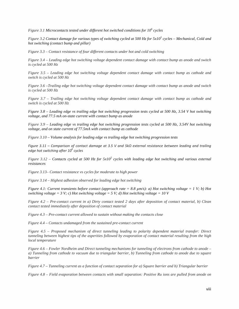
List of Figures and Tables Figures
Figure 1.1: Direct contact RF MEMS switches by various groups – a) Agilent Technologies, b) Northeastern University/Radant MEMS, c) Lincoln Laboratories, d) Omron, e)RFMD, f) University of California, San Diego
Figure 1.2 – Cross section of a P-I-N diode
Figure 1.3 – Cross section of a GaAs FET switch
Figure 1.4: Applications of RF MEMS switches
Figure 1.5 – Satellite switching network with MEMS applications highlighted
Figure 1.6 – Transceiver system with MEMS applications highlighted
Figure 2.1 – a) Test setup for in-situ testing of microcontacts, b) Schematic of the SPM based setup.
Figure 2.2 – Test setup with circuit connections
Figure 2.3 – Effective idealized circuit diagram for the setup
Figure 2.4 –a) SEM micrograph of Force sensor, b) SEM micrograph of the mating pillar, c) Schematic of the force sensor
Figure 2.5 – Circuit schematic for the main amplifier circuit
Figure 2.6 – Amplifier for piezo-actuator
Figure 2.7 – Creation of ground loop
Figure 2.8 – Schematic of the DAQ input
Figure 2.9 – Independent input at channel ai0
Figure 2.10 – Independent input at channel ai1
Figure 2.11 – Channels scanned together with ai1 having high source impedance
Figure 2.12 – Channels scanned together with ai1 having infinite source impedance
Figure 2.13 – A-B voltage with ripples indicating constructive and destructive interference between reflected laser spots from the pillar and force structure
Figure 2.14 – A-B voltage with ripples removed
Figure 2.15 – Effective circuit for four-probe measurement
Figure 2.16 – Top view of force sensor chip
Figure 2.17 – a) Voltage profile of the inner area of the chip with test structures present, b) Voltage profile of the inner area of the chip with test structures absent
Figure 2.18 – Effective circuit diagram taking into account shunt resistances
viii
Figure 3.1 Microcontacts tested under different hot switched conditions for 106 cycles
Figure 3.2 Contact damage for various types of switching cycled at 500 Hz for 5x10⁵ cycles – Mechanical, Cold and hot switching (contact bump and pillar)
Figure 3.3 – Contact resistance of four different contacts under hot and cold switching
Figure 3.4 – Leading edge hot switching voltage dependent contact damage with contact bump as anode and switch is cycled at 500 Hz
Figure 3.5 – Leading edge hot switching voltage dependent contact damage with contact bump as cathode and switch is cycled at 500 Hz
Figure 3.6 –Trailing edge hot switching voltage dependent contact damage with contact bump as anode and switch is cycled at 500 Hz
Figure 3.7 – Trailing edge hot switching voltage dependent contact damage with contact bump as cathode and switch is cycled at 500 Hz
Figure 3.8 – Leading edge vs trailing edge hot switching progression tests cycled at 500 Hz, 3.54 V hot switching voltage, and 77.5 mA on-state current with contact bump as anode
Figure 3.9 – Leading edge vs trailing edge hot switching progression tests cycled at 500 Hz, 3.54V hot switching voltage, and on state current of 77.5mA with contact bump as cathode
Figure 3.10 – Volume analysis for leading edge vs trailing edge hot switching progression tests
Figure 3.11 – Comparison of contact damage at 3.5 V and 5kΩ external resistance between leading and trailing edge hot switching after 106 cycles
Figure 3.12 – Contacts cycled at 500 Hz for 5x10⁵ cycles with leading edge hot switching and various external resistances
Figure 3.13– Contact resistance vs cycles for moderate to high power
Figure 3.14 – Highest adhesion observed for leading edge hot switching
Figure 4.1: Current transients before contact (approach rate = 8.8 µm/s): a) Hot switching voltage = 1 V; b) Hot switching voltage = 3 V; c) Hot switching voltage = 5 V; d) Hot switching voltage = 10 V
Figure 4.2 – Pre-contact current in a) Dirty contact tested 2 days after deposition of contact material, b) Clean contact tested immediately after deposition of contact material
Figure 4.3 – Pre-contact current allowed to sustain without making the contacts close
Figure 4.4 – Contacts undamaged from the sustained pre-contact current
Figure 4.5 – Proposed mechanism of direct tunneling leading to polarity dependent material transfer: Direct tunneling between highest tips of the asperities followed by evaporation of contact material resulting from the high local temperature
Figure 4.6 – Fowler Nordheim and Direct tunneling mechanisms for tunneling of electrons from cathode to anode – a) Tunneling from cathode to vacuum due to triangular barrier, b) Tunneling from cathode to anode due to square barrier
Figure 4.7 – Tunneling current as a function of contact separation for a) Square barrier and b) Triangular barrier
Figure 4.8 – Field evaporation between contacts with small separation: Positive Ru ions are pulled from anode on

ix
to the cathode leading to material transfer
Figure 4.9 – Atom-anode and atom-cathode interactions as a function of distance. The two interaction profiles do not overlap
Figure 4.10 – At small separations, the two interaction profiles to overlap. The sum of the two profiles has a double-well structure with a small activation barrier
Figure 4.11 – Leading and trailing edge hot switching tests for comparing bipolar to unipolar contact damage
Figure 4.12 – Long duration bipolar tests – a) Leading edge bipolar hot switching with 3.5 V hot switching voltage and 77.5 mA on-state current, b) Trailing edge bipolar hot switching with 3.5 V hot switching voltage and 77.5 mA on-state current, c) Trailing edge bipolar hot switching with 3.5 V hot switching voltage and 77.5 mA on-state current
Figure 4.13 – Contact resistance and contact force vs no of cycles for a long term bipolar hot switching test. Resistance is stable almost throughout the test and rises towards the end
Figure 4.14 – SPICE model of the equivalent circuit for the test setup considering the capacitance in the chip
Figure 4.15 – Transient current response for an external resistance of a) 50 Ω, b) 500 Ω, c) 5 kΩ, d) 20 kΩ, e)1 MegΩ and f)10 Meg Ω
Figure 4.16 – Contact damage with 3.5 V hot switching voltage after 106 cycles for leading edge hot switched tests with different external resistances
Figure 4.17 – Leading edge hot switching tests at 3.5 V hot switching voltage, 50 Ω resistor, with contacts separated at 8.8 nm/s: a) Contact bump is anode; b) Contact bump is cathode
Figure 4.18 – Trailing edge hot switching tests at 3.5 V hot switching voltage, 50 Ω resistor, with contacts separated at 8.8 nm/s: a) Contact bump is anode, b) Contact bump is cathode, and c) Contact bump is cathode
Figure 4.19– Trailing edge hot switching tests at 3.5 V hot switching voltage, 50 Ω resistor, with contacts separated at 8.8 nm/s: a) Contact bump is anode, b) Contact bump is cathode, c) Contact bump is cathode
Figure 4.20 – Slow tests at an approach/separation rate of 2.2 nm/s, at a voltage of 5V and external resistance of with contacts not being allowed to come apart: a) Contact bump is anode, b) Contact bump is cathode
Figure 5.1 (a) Schematic of test circuit with external resistor (b) Current spikes measured via the external resister before closing and after opening in a contact cycled at 500 Hz with 3.00VHot and 55 Ω of total series resistance
Figure 5.2 – Realistic circuit for the test setup
Figure 5.3 – Test setup with DAQ disconnected
Figure 5.4 – Current spikes in the absence of a DAQ across the contact
Figure 5.5 – a) Circuit with 1 nF capacitor, b) Circuit with co-axial cable parallel with contact, c) Current spikes corresponding to the two circuits respectively
Figure 5.6 a) Contact after 500,000 cycles with no DAQ connected, b) Contact after 500,000 cycles with DAQ in parallel
Figure 5.7 – Equivalent circuit for a simple RF system with inductance and capacitance of the switch taken into consideration
Figure 5.8 – Force vs time, Force vs Resistance and Resistance vs time for contacts with different material

x
Figure 5.9 – Current transient in an RF microswitch vs dF/dt of the switch – the black vertical line represents the dF/dt of a standard
Figure 5.10 – Current transient vs phase angle at which contact is closed – it should be noted that the current overshoot as a function of phase is plotted at a unrealistic value of dF/dt so as to amplify its magnitude
Tables
Table 1: Comparison of Switch technologies on the basis of Figure of Merit
Table 2: Dimensions of the force sensor structures used
Table 3: Thermal properties of Ruthenium Table 4: Contact damage associated with different material transfer mechanisms
Table 5: Figures associated with different material transfer mechanisms

Anirban Basu, PhD dissertation Page 1
Chapter 1 - Introduction
1.1. Overview of RF MEMS switches and their applications
Micro-electromechanical Systems (MEMS), also known as Microsystems in Europe are
miniature devices that are fabricated using process technology derived from the semiconductor
IC industry. MEMS transducers have expanded in their applications and from being a mere
research interest in the 1970s it has grown to be a nearly $9 billion industry [1].
RF MEMS switches refer to micro-electromechanical switching devices with applications
in the RF communications industry. Currently, the RF industry overwhelmingly uses solid state
switches. While solid state switches do offer advantages, MEMS switches are exceedingly useful
in two very important aspects – high isolation and low on-resistance. The predecessor to RF
MEMS switches in terms of similar performance was electro-mechanical relays. However, these
being bulky and expensive to manufacture, were never considered seriously in the RF industry.
With the advent of MEMS and with miniaturization of the geometry, MEMS switches provided a
realistic alternative for the RF industry [2,3].
The first major progress in the development of RF MEMS switches was accomplished by
Northeastern University in collaboration with Analog Devices [4,5]. Radant MEMS, a startup
that designed RF MEMS switches, spun out of this collaboration. Following that, several
companies including IBM and Motorola started pursuing this area in a major way. However, the
most successful of all has been the switch manufactured by Omron Corp. which has shown
remarkable performance and reliability. Radant MEMS too, has manufactured and
commercialized a high performance switch with high reliability and lifetime. The lifetime of the
switch exceeds several hundred billion cycles [6,7].

Anirban Basu, PhD dissertation Page 2
Figure 1.1 – Direct contact RF MEMS switches by various groups – a) Agilent Technologies, b)Northeastern University/Radant MEMS, c) Lincoln Laboratories, d) Omron, e)RFMD, f) University of California, San Diego
Functionally, RF MEMS switch is almost identical to an electromechanical relay. Thus, it
must have an actuation mechanism and should have an electrical signal transmission area. The
actuation mechanism can be one out of the following: electrostatic, electromagnetic,
piezoelectric or thermal. The electrical signal transmission is done either via a metal-to-metal
contact or a capacitive contact. In an RF circuit, the switches may be placed in series or in shunt
configuration to isolate one part of the circuit from another.
The primary competitor of RF MEMS switches are the p-i-n diodes and the GaAs FET
switches [8]. A p-i-n diode is made up of a p-doped and an n-doped region similar to a
conventional diode. However, it also has an intrinsic i-region where both p and n charges reside
[9]. This allows the p-i-n diode to behave differently from other diodes. Basically, it acts as a
conventional rectifier diode at low frequencies, but at higher frequencies it will behave as a

Anirban Basu, PhD dissertation Page 3
resistor whose resistance can be controlled by the amount of DC current passing through it.
Depending on the thickness of the i-region, p-i-n diodes can be designed such that a few mA of
DC current can result in very low resistance at RF frequencies. However, the use of DC current
as the control for these switches results in them having a high insertion loss.
Figure 1.2 – Cross section of a P-I-N diode [10]
In MESFET switches, such as the GaAs devices, the RF signal flows from Source to
Drain while the gate voltage acts as the control voltage. A major disadvantage in FET switches is
leakage current which prevents it from offering adequate isolation and lowers the off-resistance
of such switches.
Figure 1.3 – Cross section of a GaAs FET switch [11]
Anirban Basu, PhD dissertation Page 4
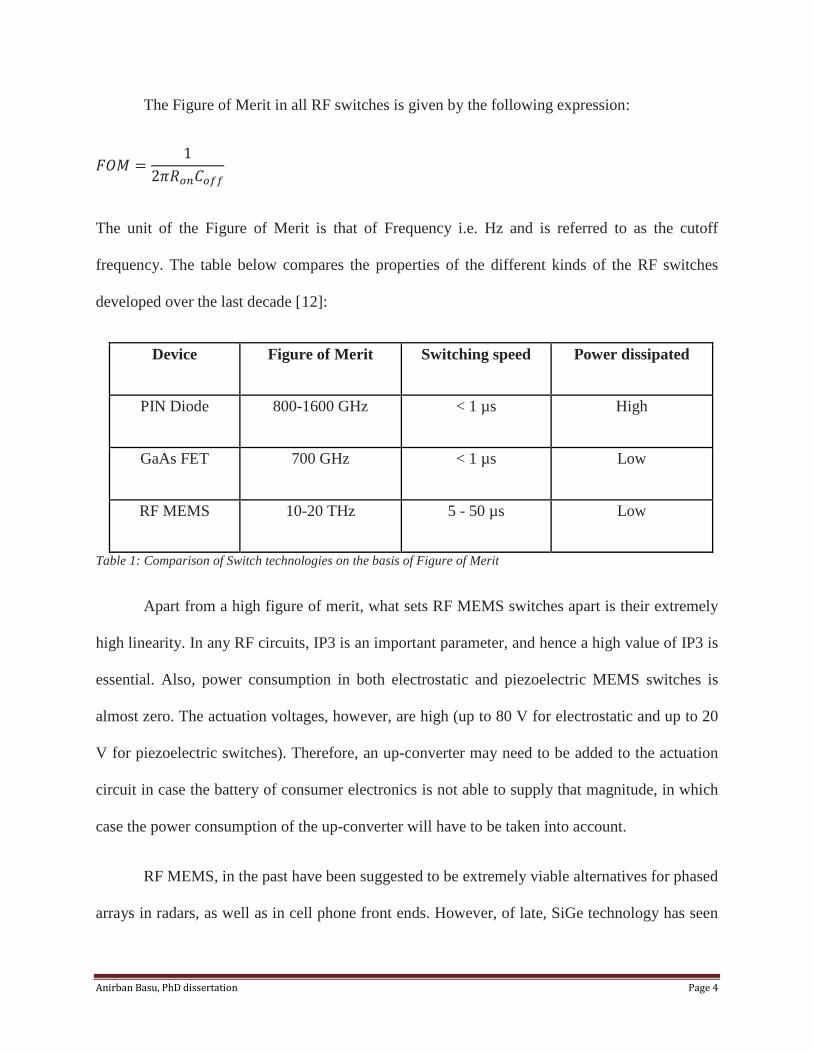
The Figure of Merit in all RF switches is given by the following expression:
𝐹𝑂𝑀 =1
2𝜋𝑅𝑜𝑛𝐶𝑜𝑓𝑓
The unit of the Figure of Merit is that of Frequency i.e. Hz and is referred to as the cutoff
frequency. The table below compares the properties of the different kinds of the RF switches
developed over the last decade [12]:
Device Figure of Merit Switching speed Power dissipated
PIN Diode 800-1600 GHz < 1 µs High
GaAs FET 700 GHz < 1 µs Low
RF MEMS 10-20 THz 5 - 50 µs Low
Table 1: Comparison of Switch technologies on the basis of Figure of Merit
Apart from a high figure of merit, what sets RF MEMS switches apart is their extremely
high linearity. In any RF circuits, IP3 is an important parameter, and hence a high value of IP3 is
essential. Also, power consumption in both electrostatic and piezoelectric MEMS switches is
almost zero. The actuation voltages, however, are high (up to 80 V for electrostatic and up to 20
V for piezoelectric switches). Therefore, an up-converter may need to be added to the actuation
circuit in case the battery of consumer electronics is not able to supply that magnitude, in which
case the power consumption of the up-converter will have to be taken into account.
RF MEMS, in the past have been suggested to be extremely viable alternatives for phased
arrays in radars, as well as in cell phone front ends. However, of late, SiGe technology has seen

Anirban Basu, PhD dissertation Page 5
advances while SOI and SOS transistors too have seen tremendous development which have
resulted in extremely inexpensive solid-state switches being manufactured with great power
handling capabilities and high IP3 value. Thus, both these areas, which were earlier thought to be
potential markets for RF MEMS, are not viable any longer. However, there are other application
areas where RF MEMS has a clear advantage over semiconductor technology [13]. These are:
1) Automated Testing Equipments or ATEs used for characterizing RF ICs. ATEs require both
DC and RF signals to pass through and metal-to-metal direct contact MEMS switches can be
extremely useful in this regard.
2) Spectrum analyzers and signal analyzers which require high linearity and also high isolation
between different ports. Currently, they often use electromechanical relays to achieve these and
scaling down to RF MEMS can only prove beneficial.
3) Wideband receivers and transmitters in defense systems which contain switched filter banks
(made up of SPDT switches) mostly use the lossy p-i-n diode switches. RF MEMS can be a
viable alternative for these.
4) Satellite switch matrices which require a huge number of switches and therefore moving to RF
MEMS will result in reduction of the bulkiness of such systems and also lead to better
performing networks [14].
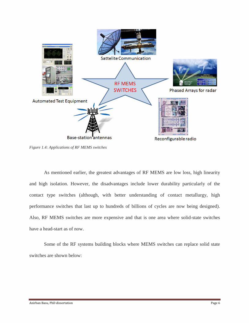
Anirban Basu, PhD dissertation Page 6
Figure 1.4: Applications of RF MEMS switches
As mentioned earlier, the greatest advantages of RF MEMS are low loss, high linearity
and high isolation. However, the disadvantages include lower durability particularly of the
contact type switches (although, with better understanding of contact metallurgy, high
performance switches that last up to hundreds of billions of cycles are now being designed).
Also, RF MEMS switches are more expensive and that is one area where solid-state switches
have a head-start as of now.
Some of the RF systems building blocks where MEMS switches can replace solid state
switches are shown below:

Anirban Basu, PhD dissertation Page 7
Figure 1.5 – Satellite switching network with MEMS applications highlighted [14]
Figure 1.6 – Transceiver system with MEMS applications highlighted [14]

Anirban Basu, PhD dissertation Page 8
1.2. Electrical contacts for MEMS switches
As mentioned before, MEMS switches can be classified into two categories based on how they
conduct the electrical signal. These are: a) Capacitive and b) Direct contact. In capacitive
switches, a dielectric separates the surfaces of the metal electrodes. RF MEMS capacitive type
switches have been designed to have insertion of <0.1 dB at tens of GHz and isolation of tens of
dB. However, one drawback of capacitive switches is its inability to conduct DC signals.
Sometimes, even in RF circuits, conducting DC voltages is essential, particularly as biasing
voltages in devices. Also, there is a reliability issue with capacitive switches which is dielectric
charging that can be affected by environmental conditions such as humidity [15].
Metal contact RF MEMS switches have received a lot of attention in the communications
industry lately since these switches have low on resistance, high isolation and are suitable for
signals with frequency ranging from DC to the millimeter wave frequencies (100 GHz) [16].
Some of the best RF MEMS switches, particularly the ones that have so far been successfully
commercialized are the metal contact type. The reliability of these switches is in a large part
related to the reliability of their electrical contacts. Much like in electromechanical relays,
therefore, the study of electrical contacts has grown to be a separate area of research by itself.
There are several different parameters of the electrical contacts that require close investigation.
As such, not a whole lot of work has been done so far in accurately trying to understand the
behavior of these contacts.
While studying contact metallurgy, a lot of thrust was placed on the electrical resistance
of these metal contacts, since low power consumption was one of the selling points of RF
MEMS switches. A lot of the very first switches designed and manufactured, therefore used Au

Anirban Basu, PhD dissertation Page 9
as the contact material [17]. The main advantages of Au were its high conductivity and also
extremely low affinity to organics. Low affinity to organic contamination meant that these
switches had an increased lifetime and suffered little in terms of increase of resistance due to
surface contamination. However, Au is a soft metal. This property prevents it from being the
ideal contact material. Softness of Au leads to high adhesion between the contact surfaces
[18,19,20]. In his work on study of contacts, Lei Chen determined that high adhesion even
during cold switching, makes Au switches prone to failure by sticking. This failure to open is one
of the primary modes of failure in MEMS switches after they have cycled for a large number of
cycles [21]. Both hot and cold welding (associated with hot switching and cold switching
respectively) have been reported to cause contact damage [22,23,24]. In order to reduce adhesion
between contact surfaces, the two electrodes of a contact have been coated with different
materials. Such contacts, however, have been shown to suffer from high resistance caused by
carbon build-up [25,26].
Carbon contamination and frictional polymer on the surface causes contacts to lose their
conductivity [21,27,28]. However, Au has better reliability in this area because of the reasons
discussed before. Contamination, though, can be reasonably prevented by hermetic packaging.
This factor led researchers to concentrate more on high adhesion and to design switches which
do not fail by stiction. For instance, low force switches suffer from much less adhesion and
subsequent failure than high force ones.
While determining reliability of switches, it is their reliability in cold switching
conditions that is mostly discussed. Hot switching is a relatively unexplored area and while it has
been known that they cause great damage to the microswitch contacts (much like in
electromechanical switches), not a great deal of literature is available on them. The difference

Anirban Basu, PhD dissertation Page 10
between cold switching cycles and hot switching ones will be explained subsequently.
Significant work has been published that studies the performance of the electric contacts
coated with different materials. For contact material, different alloys of Au have been
investigated that can improve the hardness of the contacts while retaining the conductive
properties of Au. Contact materials such as Pt and Ir have been tested by the predecessors of this
author [29,30,31]. While some of these materials have been promising they still do suffer from
high resistance after millions of cycles. Clean Ru switches, which have undergone oxygen
plasma clean and have a layer of oxide on it, have on the other hand shown excellent
performance particularly under cold switching conditions. Having been limited by the switching
rate in SPM-based contact tester, these contacts in the past hadn’t been tested for more than a
million cycles. But in this work, the author reports tests that lasted much longer without
sufficient degradation of the contact performance. It should be noted, however, that these tests
have been conducted under a constant N2 flow which means that the atmosphere around the
contact is extremely pure.
In larger electromechanical relays, one technique to avoid build-up of contamination
between contacts is to introduce scrubbing [32,33]. In micro-contacts, however, sliding is
discouraged because of the extremely thin layer of contact material present which can get
removed quickly. The absence of sliding thus makes micro-contacts susceptible to surface
contamination build-up, particularly during cold switching.
1.3. Hot Switching in MEMS switches
Although adhesion and carbon contamination can degrade the performance of electrical contacts

Anirban Basu, PhD dissertation Page 11
in MEMS switches, it is hot switching that causes the most significant damage to metal contacts.
In RF circuits, it is entirely possible that a voltage may be applied across the switch while it
transitions from off to on state or vice versa. Hot switching refers to the application of an RF
signal or DC voltage across the switch contacts during this transition process. Although it is
possible to incorporate logic so as to avoid hot switching, it is important for switches to be able
to withstand hot switching without extensive damage.
It has been observed that hot switching leads to significantly more damage and reduced
lifetime than pure cold switching. Although hot switching was not fully explored in MEMS
switches until recently, switch designers have nevertheless attempted to design switches and
contacts such that hot switching damage can be reduced. One of the more novel methods
proposed in this regard was the ball grid array dimple design by Linda Chow et al [34]. Their
switches were able to sustain more than 100 million hot switching cycles at an RF power of 1.25
W. They attributed the success of their design to a reduced contact area.
In macrorelays, it is well-established that arcing, which is a direct effect of a high voltage
across contacts having a small separation, occurs both when the contacts come together as well
as when they begin to come apart and is possibly the most significant cause of contact damage.
Arcing can cause several detrimental effects on the contact. On the one hand, such arcing can
lead to contact erosion since it will melt the contact material on either side of the arc while on the
other hand, arcing and the consequent high temperatures associated with it can also cause the
formation of oxides, nitrides, sulphides, carbonates and carbonaceous compounds by triggering
reactions with gases adsorbed by the contact material from the ambient air [33]. For
microcontacts, though, contact damage leading to failure can occur at voltages much below arc-
like conditions as explored in this thesis.

Anirban Basu, PhD dissertation Page 12
Hot switching damage in microcontacts has been analyzed from various perspectives by
different research groups. When MEMS relays were still at their inception stage in the late 90s,
their electrical contacts were studied as a part of the overall study of the reliability of the
switches. It was deduced early on that in the absence of the high voltages associated with contact
damage in macrorelays, the damage mechanisms for the MEMS relays are different. In some of
the earliest work on MEMS relays, “Microrelay design, performance and systems”, Kruglick
noted that Paschen effects and arcing are irrelevant in MEMS relays [35].
Detailed investigation of damage mechanisms and damage characteristics in the MEMS
switches was not undertaken until a few years back. There were two most prominent theories that
were proposed to explain the lifetime reduction of the contacts under hot switching:
1) Micro-arcs appear between the contacts just prior to closing and immediately after
breaking of contact. These micro-arcs decompose any organics available either in the ambient or
on the surface of these contacts, causing carbonaceous contamination to appear on the surface of
the contacts. The appearance of such carbon contamination was documented separately by at
least 2 different research groups [36,37,38]. In [38], contact damage was associated with current
transients due to parasitic inductances in the circuit which can be compensated by adding a
capacitive quenching circuit.
2) Material transfer between contacts leading to erosion of contacts finally leading to
high contact resistance. The phenomenon of material transfer was well known among macro
sized electromechanical relays and it is also fairly well understood. However, in MEMS contacts
these are not well understood. The two proposed theories in this regard are field emission and
field evaporation which have been suggested by two different research groups [39,40,41]. The

Anirban Basu, PhD dissertation Page 13
field emission theory proposes that at small distances, tunneling of electrons from cathode to
anode leads to a rise in temperature at the anode. If the energy in the electrons is high enough to
raise the temperature of the hottest area of the anode to boiling point, then material from anode
will evaporate and deposit on to the cathode. Field evaporation on the other hand suggests that
the electric field between the contacts at small separations can lead to surface atoms being pulled
out of its lattice when the electric field is greater than a threshold value. Field evaporation also
leads to material transfer from anode to cathode.
Field emission and tunneling of electrons has been studied in the past at lower voltages.
In their work in [42], Wallash and Levit suggested that at very small separations between
electrodes Fowler Nordheim current leads to small breakdown voltages, thereby giving us what
he calls the modified Paschen curve.
Another possible cause of material transfer is the formation of a metal vapor when
asperities come into contact and then evaporate due to the sudden release of capacitive energy.
The metal vapor then gets ionized and the positively charged ions are attracted towards the
cathode leading to mass transfer. During trailing edge, there is a possible formation of a metal
bridge [43,44] due to adhesion which subsequently evaporates due to the high associated
temperature forming a metal vapor that ionizes and finally gets deposited on to the cathode. This
phenomenon is similar to what is observed in macro-relay contacts and is known as arc erosion
of contact material [45,46].
There is also the possibility of material transfer due to electromigration which can be
caused due to very high current density. Such electromigration can be accelerated due to the
formation of a molten bridge [47]. Thermal effects, such as Thomson effect where the flow of

Anirban Basu, PhD dissertation Page 14
current causes a thermal gradient in a molten bridge which then leads to material being
transferred towards the cooler electrode, can also lead to material transfer [32].
The combination of all these phenomena makes it difficult to predict quantitatively how
much material transfer can occur at a given voltage. The aim of the author, in the course of his
thesis work, is to attempt to address the significance of each phenomenon and to establish
evidence of each.

Anirban Basu, PhD dissertation Page 15
Chapter 2 - Experimental setup
2.1. AFM based test setup
Fabrication of RF MEMS switches can be expensive due to a variety of reasons. Since the focus
of this work is the study of the electrical contacts, fabrication of actual switches is unnecessary.
For testing various different contact materials without having to fabricate an entire batch of chips
with a particular contact material, it is much more convenient to use test structures on which the
contact material can be deposited after the structures have been completely fabricated and
released. That way, several contact materials can be tested from chips derived from a single
wafer. In actual switches, since the contacts lie underneath the structure, it is impossible to coat
the contact with whatever material one wishes to. Coating of the contact material, therefore,
cannot be a final step and instead has to be done before release.
Also, in order to have the flexibility of studying the performance of the contacts under
varying amount of contact forces, it is necessary that a suitably adaptive method is designed. If
the tests were done on actual switches, then the study of the contacts could only be done within
the range of contact forces for which the particular switch had been designed. Figure 2.1 shows
the picture and the overall schematic of the SPM based test setup for study of contacts.

Anirban Basu, PhD dissertation Page 16
a) b)
Figure 2.1 – a) Test setup for in-situ testing of microcontacts, b) Schematic of the SPM based setup.
For study of contacts, various research groups have in the past used contact test setups.
The three most popular test facilities are – 1) Customized AFM setup, 2) Nano-indenter, 3) Pico-
indenter [24,48,49,50,51]. However, with all these systems, there is a compromise between
accuracy and speed of testing. Cycling the contacts for more than 106 cycles requires that cycling
of the contacts be performed at a fast enough rate so that the test does not prolong to days.
Among several systems implemented purely for testing of contact material, some that stand out
are those by Ma et al [24], Yunus [51] and Kwon [49]. However, lifetime tests lasting up to
millions of cycles could not be conducted with these systems and thus long term tests on
reliability of contacts and contact evolution were not performed.
Figure 2.2 shows the simplified test setup while Figure 2.3 shows the entire test setup.

Anirban Basu, PhD dissertation Page 17
Figure 2.2 – Effective idealized circuit diagram for the setup
Figure 2.3 – Test setup with circuit connections
Lei Chen, for his work on contact evolution [21], had used a cantilever beam with a
contact bump at its tip which formed one end of the contact. The other end was a flat surface.
However, by using such a cantilever structure as a force sensor, sliding effects were encountered
during the contact tests. Also, the measured resistance in this previous setup included the sheet
resistance components of the metal films on the cantilever and testing pads. A better test setup
would incorporate a four wire measurement such that the effect of sheet resistance and other

Anirban Basu, PhD dissertation Page 18
resistances on the contact resistance measurement can be minimized.
The structures fabricated and used for the tests performed during this work were designed
by a previous graduate student working in this group [31]. Lei Chen and Nikhil Joshi, students
under Professors Nick McGruer and George Adams, have also used this identical setup [30].
Fig 2.4 shows a typical force sensor and the mating pillar. The clamped-clamped beam
structure of the force sensor is fabricated from silicon and later coated with the required contact
material. The dimensions of the two different structures used for the various tests are presented
in Table 2 and then coated with a metal film. The stiffness of these force sensors with these
dimensions were found to be approximately 3380 N/m for the long beams and 8300 N/m for the
short beams using finite element analysis. The paddles on the force sensor are wider than the rest
of the beam and are used to reflect the laser from the source to a mirror which further reflects it
to the force sensor. By adjusting the mirror one can focus the laser right at the center of the photo
detector. When the mating pillar, during actuation, comes into contact with the force sensor, it
pushes it upward which causes the laser beam to move upward. On the other hand, when the
contacts are coming apart, the laser beam moves downward and may even go below its original
starting position if there is adhesion.
The pillar side of the contact is slightly raised from the rest of the chip so that proper
contact is made only between the contact bump and the pillar and not anywhere else on the chip.
Also, the clamped-clamped beam housing the contact bump ensures there is no scrubbing or
sliding between the contact surfaces.

Anirban Basu, PhD dissertation Page 19
a) b)
c)
Figure 2.4 –a) SEM micrograph of Force sensor, b) SEM micrograph of the mating pillar, c) Schematic of the force sensor
Dimension (μm)
Feature Short Structure Long Structure
Total Length 90 120
Paddle Width 40 40
Paddle Length 35 40
Middle Spacing 10 20
End Spacing 5 10
Beam Width 20 20
Beam Thickness 4.5 4.5
Table 2: Dimensions of the force sensor structures used

Anirban Basu, PhD dissertation Page 20
The relationship between the A-B voltage from the photodetector of the AFM and the
displacement of an AFM tip was found by using a calibrating sample with a known step height.
This information can then be combined with the result of a finite element model for the force
structures which can relate the displacement with the corresponding force experienced by the
structure. The results of the Finite Element Analysis concluded that the conversion factor for
transforming the A-B voltage into force is approximately 153.8 µN/V for the large structures and
for the smaller structures it is 266.67 µN/V.
2.2. Contact preparation and testing procedure
2.2.1. Contact preparation
Before the start of a test, the microchips to be tested ideally need to undergo an oxygen-plasma
clean. The purpose of the plasma clean is two-fold: a) to remove any organic surface
contaminants from the samples under test, b) to create a protective oxide layer on top of the
contacts that ensure longer durability of these contacts. In the past, it has been proven that
ruthenium oxidizes to RuO2 when exposed to O2 plasma for an appropriate amount of time [52].
Ruthenium oxide has also been shown to be stable and conductive [53]. Based on these findings
and other work by [54,55], it can be stated that a thin oxide layer will be present on the contact
surfaces at the start of any test.
Initially (up to June 2012), for samples tested within 48 hours of deposition, the test was
performed without performing the oxygen plasma clean; samples tested between 2 and 5 days of
deposition were plasma cleaned for 3 minutes; samples tested 5 or more days after deposition
were cleaned for 5 minutes. This procedure applies to tests where contact damage and material

Anirban Basu, PhD dissertation Page 21
transfer were characterized as a function of the number of hot switching cycles. Later, to
maintain more consistency between sample surfaces, all tests were performed within 72 hours of
deposition and cleaned for 3 minutes. It is important to note that the ex-situ plasma cleaning
presented above was found empirically to not affect the results of the test contacts at least for the
hot switched samples that underwent material transfer.
The system used for the oxygen plasma clean was an MKS-AX7670. The following
steps describe a typical plasma cleaning procedure:
1) The cooling water supply is turned on. The water passes through a filter before passing
through pipes that enter and leave the plasma chamber.
2) The vacuum chamber of the plasma system, at this stage, is at atmospheric pressure and one of
its outlets is open. The chamber is manually lifted and the samples that need to be cleaned are
placed inside the chamber.
3) The plasma system is turned on by switching on the power switch. There is an display screen
on the plasma system which displays various messages depending on system conditions. When
the screen says ‘READY’, the user would know that the next steps can be carried out.
4) The vacuum pump is turned on. At this stage, the vacuum chamber of the plasma is still
disconnected from the pump via the main valve. This valve should not be opened until the user is
ready to close the chamber by shutting the open outlet with an O-ring and KF flange.
5) The main valve is gradually opened after the chamber is closed.
6) The pressure in the chamber will now begin to drop. If the pump is functioning properly, this
drop in pressure (monitored with a pressure sensor) occurs very rapidly within 4-5 seconds.

Anirban Basu, PhD dissertation Page 22
7) When the pressure is around 200 mTorr, the Ar supply is turned on at a flow rate of 0.5 sl/m.
The software used for controlling the gas supplies is Smartrak.
8) The pressure in the chamber should now start to increase. Once there is a stead pressure of
1200-1300 mTorr, the voltage to fire the plasma can be turned on. The voltage supplied is a DC
voltage of 24 V. This is pure Argon plasma with no Oxygen in it.
9) Oxygen at a flow rate of 0.15 sl/m is now started. It takes about 6-7 seconds for the software
to trigger the Oxygen supply.
10) When the oxygen starts flowing into the chamber, the plasma changes its color. From being a
dim purple color, the plasma transforms into a bright purple color.
11) In steps of 0.05 sl/m, the Oxygen flow rate is ramped up to 0.5 sl/m
12) In steps of 0.05 sl/m, the Argon flow rate is now ramped down to 0.3 sl/m.
13) At a ratio of 5:3 of O2:Ar the plasma clean is done.
14) At the end of the clean, the DC voltage supply which supplies current to the plasma is turned
off.
15) The main valve is then shut closed thus cutting off the vacuum pump from the plasma
chamber.
16) The Argon and Oxygen supplies are then turned off.
17) The chamber is now purged with atmospheric air by slowly pulling out the gate of one of the
outlets of the chamber. There are a total of 4 hoses with KF flange. One is connected to the
vacuum pump, one is connected to the pressure sensor. Out of the remaining two hoses, opening

Anirban Basu, PhD dissertation Page 23
either one can purge the chamber and bring it back to atmospheric pressure.
18) The chips can now be taken out by manually lifting the plasma chamber. The user should
also remember to shut down the main power supply to the plasma system.
2.2.2. Contact testing procedure
Setting up of an experiment, after the oxygen plasma treatment of the contacts, begins with
placing the chips on their respective holders. For the force sensors, the AFM tip holder itself acts
as the tool where the chip is mounted. However, for the pillars, a specially designed metal plate
structure has been made with help from the Machine shop. The holder has a center region carved
at an inclination of 120. This is the angle which the AFM tip makes with the horizontal axis
when it is placed on the holder. To match this angle, the opposite pillar must be placed at the
same angle too. The piezoelectric actuator is mounted on top of the metal plate and on top of that
the chip for the pillar is placed. Two metallic springs are placed on either end of the pillar
performing the dual responsibilities of providing mechanical support for the pillar as well as
electrical connectivity. Wires are soldered to both the metallic springs to provide connectivity to
the external devices (DAQ).
Mounting and perfect alignment of the pillar is particularly difficult. A pair of tweezers is
used for the mounting process and care must be taken while sliding the pillar underneath the
springs and on top of the piezoelectric actuator. The pillar chip must lie flat on top of the
actuator. Any inclination at any angle will cause misalignment resulting in imperfect contact.
Also, the user has to make sure that he doesn’t scratch the surface of the chip since even a minor
scratch can introduce particles that are hard to get rid of. It is also necessary to wear gloves

Anirban Basu, PhD dissertation Page 24
during mounting to avoid contamination from skin contact.
After mounting both the force sensor chip and the pillar chip, the following steps must be
taken. A lot of these steps are identical to what one does during a normal AFM scanning process.
However, in this case the AFM tip is replaced by the force sensor chip.
1) The AFM laser spot is focused on the right paddle of the force sensor. Out of the three force
sensors, generally the sensor in the middle was used.
2) Turn on the SPM scanning software and set the SPM to contact mode. The reference can be
set at 0.2 V.
3) Make sure that the laser spot as detected by the photo-detector is exactly at the center where
the x-axis meets the y-axis. The laser spot can be adjusted by turning “Check PD” on and then
manipulating the mirror which reflects the laser after it has been reflected by the paddle.
4) The pillar holder is placed where samples for AFM scanning are usually placed. Also, one
must remember to connect all the wires from pillar, force sensor and the piezoelectric actuator to
the external equipment.
5) Make sure that the pillar lies approximately below the force sensors and can be seen through
the backside window that has been etched to make this visibility possible.
6) Start moving the pillar upwards with the coarse adjustment screw. This can be done up until
the pillar and force sensor are roughly at the same focal length. At this stage the x and y axes of
the pillar holder may be adjusted so that the pillar is right underneath the force sensor under
measurement.
7) Turn on ‘Check PD’ and make sure the laser alignment is still ok. The laser will remain on

Anirban Basu, PhD dissertation Page 25
during the course of the experiment.
8) Turn ‘Retract off’ so that AFM’s own piezoelectric device can now be controlled by the
control system of the AFM. Now, click ‘Approach on’. One should remember that the reference
voltage for the AFM has been set at 0.2 V while the initial voltage is at 0 V.
9) The stepper motor now turns on and gradually pushes the pillar upwards in steps of a few nm.
When the pillar just barely touches the force sensor, and the AFM voltage increases to 0.2 V, the
control system ensures that the stepper motor turns itself off.
10) Now we apply 40 V on to the piezoelectric actuator (PI 022). Since the AFM control system
is still on and its job is to keep the A-B voltage fixed at 0.2 V, any expansion of the external
piezo will result in shrinking of the AFM’s piezo such that the A-B voltage does not alter.
11) Now we go to the ‘Advanced’ tab of the SPM software and turn the control system off by
putting the tip on hold.
12) The voltage that was hitherto applied to the external piezoelectric actuator will now be
turned off resulting in its shrinking. However, since the control system is off, AFM’s piezo will
not expand back. This will result in the pillar de-engaging from the force sensor and contact.
13) At this stage, if we apply a voltage across the contact and external series resistor, the entire
voltage should appear across the contact. If it does not that would mean the pillar chip is making
contact with the force sensor chip at some point other than the actual intended contact spots i.e.
the bump. Usually this would mean that the AFM stage where the pillar has been placed needs to
be brought back down, the pillar holder removed, and the pillar readjusted. Sometimes it could
also mean that the piezoelectric actuator itself is not working anymore. That implies that when

Anirban Basu, PhD dissertation Page 26
40 V was applied across the piezo, it in fact did not expand. The lifetime of the piezos, however,
is at least 10 billion as per the specifications. It is, therefore, very uncommon to find the piezo
not working. Changing the piezo should be the last resort after verifying without a shadow of
doubt that the alignment is indeed perfect.
14) After the pillar and the contact bump have de-engaged, a ramp-hold-ramp voltage a voltage
of about 50 V amplitude is applied.
15) It should be ensured that contact between the electrodes synchronize with the increase in A-
B voltage. Presence of electrical contact is monitored by observing the voltage across the contact
and the external resistor. At electrical contact, most of the voltage drop will be across the 50 Ω
external resistor. Also, we know that mechanical contact is monitored by observing the A-B
voltage. Thus is mechanical and electrical contact synchronize perfectly, the test setup is
working as it should.
16) The Test program software, built with LabVIEW, lets the user monitor the number of
switching cycles undertaken. All other details, including ramping rate, contact resistance, and
required contact force is available on the screen.
17) A new addition to the test program is a control system which controls the voltage applied to
AFM’s piezo. By increasing and decreasing this voltage, any piezo drift, in either direction, can
be compensated for. For allowing the program to control the voltage on AFM’s piezo, the user
needs to be on the “Advanced” tab of the SPM software and turn on ‘External Z-control’.
18) The program will run unless stopped. When force control is on, the program also stops by
itself if the AFM’s piezo has drifted too far away and the required contact force cannot be
reached even by applying the maximum voltage to the piezo. Also, if the contact resistance
Anirban Basu, PhD dissertation Page 27
becomes too high, indicating failure of the contact, the test program will stop.
19) For tests where an extremely slow approach/separation rate is used, a separate program is
used for actuating the piezo. This program is built such that the voltage to the piezo can be
gradually increased, decreased or kept constant.
The author acknowledges the major contribution by Ryan Hennessy who designed the
software for the test setup and made it easy for the author to conduct tests under various
conditions. This enabled a detailed study of microcontact behavior.
2.3. Electrical circuits for contact testing
2.3.1. Contact resistance measurement circuit
As mentioned before, the measurement of contact resistance is done using a four-probe
measurement setup. Since constant data acquisition during the course of a test is of paramount
importance, the test setup needed to be interfaced with a computer. LabVIEW was used as the
data acquisition (DAQ) software. As far as supplying voltage and current to the samples is
concerned, there can be two approaches to it: a) Using an external power supply, b) Using the
LabVIEW DAQ. There are two voltages here that need to be supplied: 1) the voltage applied to
the switch and the external resistor in series; 2) the voltage applied to the piezoelectric actuator.
In the HERMIT program, students in the past have used external power supplies for generating
these voltages. The current source for the contacts used to be generated with a DC power supply
while the voltage to the piezoelectric actuator was supplied with a function generator. The author
himself, for some preliminary investigation on the contacts, used this same setup. However, for
most conditions of leading edge and trailing edge hot switching tests, as well as for pure cold

Anirban Basu, PhD dissertation Page 28
switching tests, where contact voltages for the off state and on state segments of a cycle are
different, an external non-programmable power source was inadequate. Even with a
programmable power source, synchronizing it with a separate voltage source for the piezoelectric
actuator, is impossible. Such synchronization, of course, is necessary so that the ramping voltage
applied to the piezoelectric actuator is applied at the same time as the leading edge hot switching
voltage is applied to the contacts. For trailing edge, the contact voltage is removed as soon as the
ramping voltage is brought down to zero. Only for pure hot switching tests is the contact voltage
applied constantly.
These voltages, therefore, were required to be generated using a DAQ and had to be
generated programmatically. NI PCI-6251 DAQ board was used for interfacing the LabVIEW
software with the contact test-setup. One issue with using the DAQ to directly supply voltages to
the contact was that the internal circuit of the DAQ limits the current that can be generated. This
would limit the study of contact behavior only under low power conditions. It was necessary,
therefore, to interface the DAQ with the test setup using a driver circuit consisting of a buffer
amplifier with a voltage gain of 1 as shown in Figure 2.5.

Anirban Basu, PhD dissertation Page 29
Figure 2.5 – Circuit schematic for the main amplifier circuit.
The buffer amplifier circuit, used for supplying current to the contacts, consists of the
input voltage buffer, four different current-limiting input resistances. Also, TVS diodes and
capacitors are included for protection.
As mentioned, the buffer amplifier was necessary so as to enable the circuit to drive high
currents up to 1 A. Bypass capacitors were added from the positive and negative voltage supply
rail to the ground. These bypass capacitors have the function of controlling and restricting any
high and low frequency oscillations in the power supply.
Figure 2.5 shows the overall schematic of the amplifier circuit. The four resistors chosen
as current controlling resistors are 5 Ω, 10 Ω, 20 Ω, and 50 Ω. In standard RF circuits, the load
impedance is usually 50 Ω. For this purpose, most tests done in order to investigate contact
properties are done with 50 Ω in series. It should be noted, though, that the characteristic
impedance of the interconnects between the resistance, to contact to ground can cause the
voltage appearing across the contact to fluctuate particularly during opening and closing of the

Anirban Basu, PhD dissertation Page 30
switch at a high frequency. This is due to the characteristic impedance of a transmission line not
matching the load impedance [56] leading to reflection and re-reflection of the wave. Thus, it
was decided that a 50 Ω terminator, as shown in Figure 2.2, needs to be used. By using a
terminator, whose resistance was equal to the characteristic impedance of the co-axial cable
connecting it to the contact, this problem was addressed. Thus, instead of using a 50 Ω resistor
before the contact, the resistor was used after the contact.
The signal, therefore travels through the contact structure and then to the mating pillar
and finally through the terminating resistor. The other ends of the structure and the pillar are
connected to voltage measuring probes which are then connected to the DAQ break-out box
through a BNC. Since, it is important to protect the DAQ from current spikes or over-voltages, a
protection circuit consisting of a parallel combination of TVS (transient-voltage-suppression
diode) diodes and a capacitor was included. This protection circuit also contains a series
resistance. The TVS diode will limit the voltage to a safe limit of +/- 10 V [57]. This circuit was
originally designed as the test setup for the Northeastern University Microswitch, by Brandon
Jalbert [58].
An interface circuit was also required for the piezoelectric actuator and will be discussed
in detail later. The maximum voltage that can be supplied by the DAQ is +/- 10 V. This is
insufficient if one has to generate any significant expansion of the actuator. A voltage of 50 V
can result in an expansion of approximately 1.1 µm for the piezo used i.e. PL 022.31 [59]. Thus,
yet another amplifier, this one with voltage gain, is required for applying the requisite voltage to
the actuator.
The DAQ is connected to the test setup in two different ways. The two amplifier circuits,

Anirban Basu, PhD dissertation Page 31
which are on a PCB, are connected using a National Instruments GPI bus. The pin diagram for
this GPI bus is provided by National Instruments. For measuring the contact voltage, a BNC
cable is used to connect the leads from the contact measurement circuit to the break-out box from
the DAQ. The break-out box of the DAQ has several channels for providing both input and
output signals. For our setup, the break-out box was used solely for the purpose of measuring
signals. The measurement of voltages and the issues encountered while doing so will be
discussed later.
2.3.2. Piezo-actuator amplifier circuit
The circuit for the piezo-actuator was originally developed to supply voltage to the gate of the
RF MEMS switch developed at Northeastern University [58]. Figure 2.6 shows the power
amplifier circuit board for the piezo-actuator. The part number for this power amplifier is PA85
from Texas Instruments. The amplifier is connected in a non-inverting mode with feedback
resistors. TVS diodes and capacitors are included for overvoltage protection of the DAQ similar
to the protection provided in the main amplifier circuit described in the previous section. The
amplifier is capable of handling supply voltages of 450 V single ended or ±225 V differential. A
current limiting resistance of 30 Ω, as recommended by the manufacturers was added to limit the
current to 39 mA [60]. This is the maximum suggested current limiting resistance value. The
amplifier was designed for a gain of 21. Since the DAQ can output a maximum voltage ±10 V,
therefore the maximum available voltage from the output of the power amplifier was ±210 V
unless limited by the supply voltages. Also, the manufacturers recommended a phase
compensation impedance. This consisted of 330 Ω (RC) and 10 pF (CC) in series [60]. To prevent
the amplifier from getting damaged, 200 V rated unidirectional TVS diodes were placed on the

Anirban Basu, PhD dissertation Page 32
positive and negative rails. These will help avoid overvoltage and also protect against voltage
reversals.
Here too the effect of oscillations caused by the power supplies was accounted for. In
order to control the oscillations, a 200 V rated 1 μF and another 0.1 μF bypass capacitors were
placed in parallel from positive and negative supply voltages to ground.
Figure 2.6 – Amplifier for piezo-actuator
2.4. Measurement of voltages with LabVIEW DAQ
An integral part of the test setup jointly designed by this author is its ability to acquire data
continuously through the period of a complete test. As mentioned before, some of these tests can
run for 107 cycles at 500 Hz, which required seamless integration of the DAQ board, the
interface circuits, the switch contacts and the LabVIEW software. In LabVIEW, creation of
channels is required before data can be acquired. Some of the issues that need to be addressed in

Anirban Basu, PhD dissertation Page 33
order to enable accurate Data acquisition are a) Avoiding ground loops, b) Determining ground
reference setting of the Analog input of the DAQ, c) Avoiding ghosting. Each of these issues will
be subsequently addressed and described in detail. Among these issues, the formation of ground
loops is especially important since apart from the interface amplifier circuits, certain low level
currents in the hundreds of nA regime need to be monitored by including an additional
transimpedance amplifier. While the necessity, application and construction of this circuit will be
described in detail later, the issue of ground loop which is common to the system as a whole is
being addressed below.
2.4.1. Avoiding ground loops
During any low level current and voltage measurements, ground loops can introduce avoidable
noise in a signal. Ground loops arise when there is more than one connection to ground. For
example, in our setup, the DAQ has its own ground which is connected to the earth ground
through the computer; the op-amps both for the main amplifier circuit connected to the switch as
well as the amplifier circuit for the piezoelectric actuator have two grounds. Now, if these
different grounds are connected to the same ground bus, a loop can be formed causing a small
amount of voltage drop between the grounds. While for larger voltages such ground loops may
introduce insignificant amounts of noise, for smaller voltages and currents which may be present
in the circuit, such noise can prove to be significant. The current caused due to the presence of
such ground loop will result in a voltage drop in series with the source voltage. If the current
through the ground bus is I and the resistance from one ground connection to another is R then
the voltage drop through the ground bus → VG = IR. A schematic of this is shown in Figure 2.7.

Anirban Basu, PhD dissertation Page 34
Figure 2.7 – Creation of ground loop [61]
In order to avoid the ground loop issue, the remedy is to have independent power sources
for all the instruments used in the setup. All the grounds of these power sources and other
circuits should then be connected to a single node which goes to a common ground. For our
setup, since the DAQ is already grounded through the ground of the computer, this was chosen
as the common ground node.
2.4.2. Ground reference setting
In a DAQ, the analog input channels used for acquiring the signals are marked as AI. The circuit
for analog input ground-reference settings is designed to be able to choose between differential,
referenced single-ended, and non-referenced single-ended input modes. It is possible for each
individual AI channel used for measuring voltages to use a different mode. For most of the
signals measured by us, the signals were sent to the DAQ through a breakout board with BNC
inputs. For our setup it was important to choose the right setting for each individual channel.

Anirban Basu, PhD dissertation Page 35
Both in the breakout board as well as in the LabVIEW program, the reference setting needed to
be mentioned. For our setup, since the applied voltages are also being applied by the DAQ whose
signals are referenced to DAQ ground (referred to as AI GND), the voltages too are ground-
referenced. The only exception to this is the voltage across the resistor which is a differential
voltage. However, strictly speaking the differential voltage across the resistor is also a ground
referenced one since the voltages at the two ends of the resistor are each independently referred
to the earth ground and not floating voltages.
In the differential mode, the voltage is measured between a pair of input nodes. In the
LabVIEW DAQ, certain pins are paired to each other and in the differential mode, the voltage
for these pins will have to be measured in pairs. Thus, when the interconnections on the PCB are
designed so as to measure the voltage across resistor, it has to be ensured that the correct pair of
pins on the DAQ’s GPI-bus is connected to the ends of the resistor. An arbitrary pair cannot be
chosen since there are only specific pairs that are meant to measure such differential voltages.
For instance, for differential measurements, AI 0 and AI 8 are the positive and negative inputs of
differential analog input channel 0. Similarly, the following signal pairs also form differential
input channels: <AI 1, AI 9>, <AI 2, AI 10>, <AI 3, AI 11>, <AI 4, AI 12>, <AI 5, AI 13>, <AI
6, AI 14>, <AI 7, AI 15>, <AI 16, AI 24> and so on. In our setup, the <AI 16, AI 24> pair was
chosen for measuring voltage across the one of the four resistances. However, if the 50 Ω
terminator is used as the external resistance, then one of the channels on the breakout board is
used as the input.
2.4.3. Ghosting
If the scanned channel of a DAQ is connected to a source with high impedance, then the settling

Anirban Basu, PhD dissertation Page 36
time for the DAQ increases. This is because the ADC has a small internal capacitance which
charges or discharges as the multiplexer selects different channels of the ADC. The multiplexer
in between the source and input switches from one channel to another depending on the order in
which the LabVIEW program commands it to as shown in Figure 2.8. The source impedance,
will combine with the capacitor that is being charged to form a low pass filter whose time
constant increases with increases in the source impedance. The schematic of the circuit is shown
below:
Figure 2.8 – Schematic of the DAQ input [62]
When the multiplexer is at channel ai0 for example, it charges to a particular value.
Subsequently, the multiplexer switches to the next channel that it needs to scan, say ai1. At this
point the capacitor will charge from the voltage it was at the moment of disengagement from the
previous channel and up to the voltage on the new channel. Note that the new voltage may be
greater or less than the old voltage. If source resistance RX is too large, then the capacitor C will
take too much time to be either charged or discharged to the voltage corresponding to the new

Anirban Basu, PhD dissertation Page 37
channel. Instead it might contain some residual voltage from the previous channel scanned and
that will be clearly evident. This shadow effect due to the time constant associated with the
charging and discharging of the capacitor is sometimes called ghosting. An example of ghosting
is shown below. Here, we assume R1 is too large whereas R0 is reasonably small. If the channels
are scanned independently and not as part of a common program, then the values read are
accurate (Figure 2.9 and 2.10). If, however they are both scanned concurrently, then a shadow
effect from channel ai1 is evident on the reading of channel ai0 (Figure 2.11).
Figure 2.9 – Independent input at channel ai0[62]
Figure 2.10 – Independent input at channel ai1[62]

Anirban Basu, PhD dissertation Page 38
Figure 2.11 – Channels scanned together with ai1 having high source impedance [62]
We will face this same problem if channel ai1 is disconnected while the program is
asking it to be scanned (Figure 2.12). In that case, because of the infinite source impedance, the
capacitor will not charge or discharge from its previous value from channel ai0.
Figure 2.12 – Channels scanned together with ai1 having infinite source impedance [62]
Having realized the root cause of ghosting, several remedies can be suggested. These are
recommended by National Instruments and were strictly adhered to while writing the code for
the data acquisition as well as making the circuit connections:

Anirban Basu, PhD dissertation Page 39
i) Use of low impedance sources is always recommended since this can reduce the time
constant for the low pass filter.
ii) Scanning rate should be made only as fast as required for capturing accurate data. Too
high of a scanning rate leading to more data points may not be a good idea since that would give
the capacitor less time to settle in between transitioning from one channel to another.
iii) It is advisable to choose wisely the order in which the channels are scanned. Two
channels whose voltages have similar values can be placed one after another whereas the channel
with a voltage of a different range can be placed afterwards. It is also a good idea to place the
channels in either ascending or descending order of the magnitude of voltages they measure.
2.4.4. A-B voltage from the AFM photodetector
Another issue that had to be addressed before accurate data could be acquired was the A-B
voltage of the AFM photodetector. The A-B voltage is the signal that the photodetector of the
AFM generates when the AFM tip scans the surface of a sample. A change in the position of the
AFM tip corresponds to a shift in the laser point which is then detected by the photodetector and
interpreted as a change in voltage.
In the context of the contact testing structures, A-B voltage is directly related to the
contact force as explained earlier, since the A-B voltage changes as a result of the pillar striking
against the clamped-clamped structures with the contact bump. Under a normal circumstances,
the change in A-B voltage should be easy to detect and interpreted in terms of contact force.
However, in our setup, the laser point, apart from shining on the paddle of the force structure,
also shines on the pillar when it is very close to the force structure. The reflected signal from the
pillar interferes with the signal from the structure and can either prove to be constructive

Anirban Basu, PhD dissertation Page 40
interference or destructive depending on where the pillar is positioned. This led to the following
A-B signal shown in the figure below.
Figure 2.13 – A-B voltage with ripples indicating constructive and destructive interference between reflected laser spots from the pillar and force structure
As seen in Figure 2.13, there is a ripple right before contact force starts increasing and
right after the contact force has gone back to 0 µN. This ripples are due to constructive
interference which increases the A-B voltage thus giving an illusion of increase in contact force,
and then decreasing the A-B voltage which again makes us think the pillar has come out of
contact.
To work around this problem, the resolution was to focus the laser as well as possible. It
was observed that by manipulating the focus of the laser, the ripples can become greater or less
in magnitude. At a particular focus, the ripple would be least significant which corresponds to
the point where the focus is the best and almost the entire laser beam strikes against the paddle of
the force structure and very little of it spills on to the pillar. Given below is the A-B voltage
corresponding to a properly focused laser.

Anirban Basu, PhD dissertation Page 41
Figure 2.14 – A-B voltage with ripples removed
As seen from Figure 2.14, on properly focusing the laser beam, the ripple is practically
removed thereby enabling us to capture accurate contact force data.
2.5. Calculation of contact resistance
The purpose of monitoring the contact and resistor voltages with the DAQ is to enable us to
estimate the contact resistance during the course of cycling of the contacts. Along with
monitoring the contact force, monitoring contact resistance is of utmost importance in order to
characterize the behavior of the contacts through many cycles. While measurement of contact
force is done directly by calibrating the A-B voltage from the photodetector, monitoring the
contact resistance is done indirectly by using the four-probe approach as shown in Figure 2.15.

Anirban Basu, PhD dissertation Page 42
Figure 2.15 – Effective circuit for four-probe measurement
Because of fabrication issues as well as the design of the chips, the contact resistance
calculated using the measured contact voltage was not entirely accurate. Given below is the
design of the chip with the force structures.
Figure 2.16 – Top view of force sensor chip
As seen from the design shown in Figure 2.16, there are three structures on each chip.
This design was chosen to enable more no of samples to test per chip. However, when current
flows through the contacts, the two other structures give an alternate path for the current to flow.
This needs to be factored into an electrical model of the chip in order to arrive at an accurate
value of the contact resistance.
The second issue, essentially a fabrication deficiency, has to do with isolation trenches.
On the chip, the isolation trenches are built in between the two areas where measurement probes

Anirban Basu, PhD dissertation Page 43
are placed. These two areas are the inner rectangle and outer periphery. The reason behind
building the trenches is as follows: at the time of electrical contact and flow of current, it has to
be ensured that the path of current flow can only be through the structures so that the contact
resistance is the only resistance encountered by the current. In the absence of trenches, the sheet
resistance of the chip may become significant.
The isolation trenches are 1 µm deep and are etched all the way through the Silicon
Dioxide layer of the SOI (refer to the fabrication steps in the appendix). After release of the
structures, the contact material is deposited by sputtering whereby the entire chip gets coated
with the contact material. Sometimes, the presence of a small particle in the trench ensures that
the trenches do not end up being isolation layers, since the contact material gets deposited on
these particles too and gives the current an alternate path to flow much like the alternate paths
through the untested structures. While considerable effort was put into ensuring that the particles
are completely removed by refining the cleaning process and trying an ultrasonic clean, there
always remained some additional unwanted particles in the trenches. This gave rise to what we
called the “Shunt path” for the current and had to be characterized and included in the electrical
model of the contact system.
To study the presence of the shunt resistance, a four wire measurement to characterize the
surface current on the chip was made. The test was done as follows: Using a probe station, two
probes were placed on either side of the trenches (inner and outer). Using Keithley 237 Source
Measure Unit in its four probe mode (also known as Remote operation), a current was supplied
between these two probes. A third probe was placed next to the first source probe. The fourth
probe was navigated throughout the entire area of the inner portion of the chip to measure the
voltage at each of these points with respect to the third probe. This is a standard four-probe

Anirban Basu, PhD dissertation Page 44
measuring approach and the aim was to determine where current flows.
In the presence of the force structures, current should be flowing in the direction of the
structures since they provide the path of least resistance. However, if the structures are removed,
current should flow towards the particle in the trench that has been coated with contact material,
since that offers the path of least resistance. The figures below show both these cases and tell us
how the shunt path has a tangible effect on flow of current.
-20
-15
-10
-5
0
5
10
15
0
2
4
6
810
01
23
45
Pot
entia
l(in
mV
)
X Data
Y Data
Potential versus position (with test structures)
-20 -15 -10 -5 0 5 10 15
-15
-10
-5
0
5
10
15
24
68
1012
14
24
68
Pot
entia
l (in
mV
)
X Data
Y Data
Potential vs position (without test structures)
-15 -10 -5 0 5 10 15
a) b)
Figure 2.17 a) Voltage profile of the inner area of the chip with test structures present, b) Voltage profile of the inner area of the chip with test structures absent
Figure 2.17 a) and b) clearly show that in the presence of the test structures, the current
flows in a particular direction whereas in their absence it flows in a different direction. However,
ideally one would expect zero current flow in the absence if the test structures and zero potential
drop across the tested area.
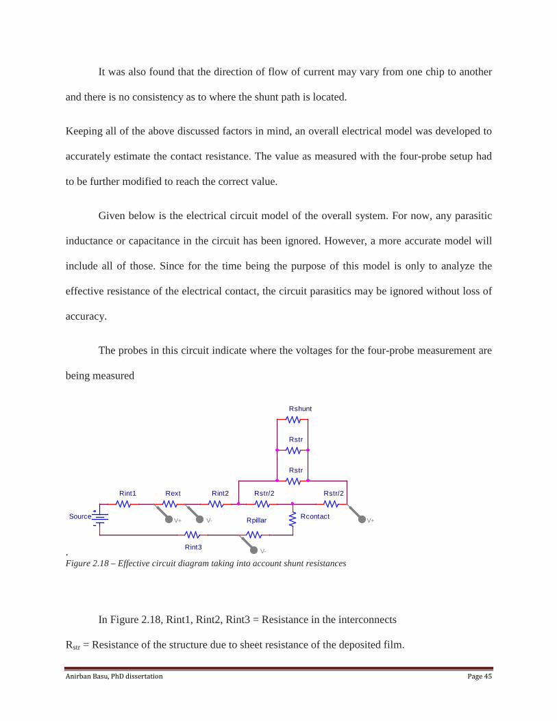
Anirban Basu, PhD dissertation Page 45
It was also found that the direction of flow of current may vary from one chip to another
and there is no consistency as to where the shunt path is located.
Keeping all of the above discussed factors in mind, an overall electrical model was developed to
accurately estimate the contact resistance. The value as measured with the four-probe setup had
to be further modified to reach the correct value.
Given below is the electrical circuit model of the overall system. For now, any parasitic
inductance or capacitance in the circuit has been ignored. However, a more accurate model will
include all of those. Since for the time being the purpose of this model is only to analyze the
effective resistance of the electrical contact, the circuit parasitics may be ignored without loss of
accuracy.
The probes in this circuit indicate where the voltages for the four-probe measurement are
being measured
. Figure 2.18 – Effective circuit diagram taking into account shunt resistances
In Figure 2.18, Rint1, Rint2, Rint3 = Resistance in the interconnects
Rstr = Resistance of the structure due to sheet resistance of the deposited film.
RextRint1 Rint2 Rstr/2
RcontactRpillar
Rstr/2
Rstr
Rstr
Rshunt
Source
Rint3
V-V+
V-
V+

Anirban Basu, PhD dissertation Page 46
Rshunt = Resistance of the shunt path.
Rext = External current controlling resistor in series with contact.
Rcontact = Actual contact resistance.
Rpillar = Resistance of the pillar due to sheet resistance of the deposited film.
Effective measured resistance =
𝑅𝑠𝑡𝑟24
𝑅𝑠𝑡𝑟 +𝑅𝑠ℎ𝑢𝑛𝑡 × 𝑅𝑠𝑡𝑟
2𝑅𝑠ℎ𝑢𝑛𝑡 + 𝑅𝑠𝑡𝑟
2
+ 𝑅𝑐𝑜𝑛𝑡𝑎𝑐𝑡 + 𝑅𝑝𝑖𝑙𝑙𝑎𝑟

Anirban Basu, PhD dissertation Page 47
Chapter 3 - Hot and Cold Switching – baseline tests and empirical results
The primary objective of this thesis is to understand and characterize the damage in the micro-
contact of a MEMS switch while also determining the damage mechanisms. To this end, the
primary tests undertaken and described in this chapter have looked at switch behavior under
different conditions – viz. different current and voltage values. The test results that are described
here are both qualitative and quantitative. While qualitative data consists of images under a
Hitachi SEM, the quantitative data looks at the volume contact material transferred. A large part
of the damage characteristics of the contacts consist of material transfer from one electrode to
another. Therefore, a volumetric analysis was important in order to quantify the damage. Also,
the contact resistance was monitored using the experimental setup in order to ensure that the
contacts did not completely fail at any point. Contact force was set at 400 µN for all tests.
Volumetric measurements were taken using the same AFM but in its conventional
scanning mode. Using the tapping mode of scanning, high resolution images were captured and
the data points thus captured were used to determine the volume of material added or subtracted.
By comparing the damaged area of the contact to the surface fit of the undamaged area of the
contact, the volume of material added to or subtracted from the contact could me calculated [63].
3.1. Hot switching damage – A complex phenomenon.
Hot switching damage can be a result of a variety of different mechanisms that are at play. Over
the last several years, a number of different mechanisms that lead to material transfer and contact
damage have been proposed [38,39,40,41,64,65]. Notable among these theories are field

Anirban Basu, PhD dissertation Page 48
emission, field evaporation, capacitance and inductance in the switch leading to voltage
overshoots, and also formation of a metal bridge which was experimentally observed in Au
microcontacts [65]. This thesis describes how complex the hot switching damage in contacts is
and how it cannot be explained by any simple model. While one or more of the mechanisms
discussed by other groups may well contribute to damage to the contact, there are almost
certainly a number of events occurring simultaneously. It can be stated that the contact damage
observed is due phenomena occurring in three domains that are coupled to one another – a)
Electrical, b) Thermal and c) Mechanical. The investigation presented in this thesis attempts to
address the phenomena due to these three domains.
To add to the complexity, not all mechanisms operate with the same intensity under all
conditions. There are certain voltage regimes where one mechanism gets precedence on another.
Also, as mentioned before, thermal mechanisms can become more prominent only at the trailing
edge and not at the leading edge. While these voltage regimes are discussed in detail later, it is
pertinent to show some of the types of observed contact damage and how the nature of the
damage can vary depending on the conditions in which the hot switching cycles took place.

Anirban Basu, PhD dissertation Page 49
a) b) c)
d) e) f)
g) h) i)
Figure 3.1 Microcontacts tested under different hot switched conditions for 106 cycles: a) Leading edge hot switching voltage of 0.5 V and on-state current of 77.5 mA with contact bump as anode, b) Leading edge hot switching voltage of 1.0 V and on-state current of 77.5 mA with contact bump as anode, c) Leading edge hot switching voltage of 2.0 V and on-state current of 77.5 mA with contact bump as anode, d) Leading edge hot switching voltage of 3.5 V and on-state current of 77.5 mA with contact bump as cathode, e) Leading edge bipolar hot switching voltage of 3.5 V and on-state current of 77.5 mA, f) Trailing edge hot switching voltage of 3.5 V and on-state current of 77.5 mA with contact bump as cathode, g) Leading edge hot switching voltage of 3.5 V and on-state current of 77.5 mA with contact bump as anode, h) Trailing edge hot switching voltage of 3.5 V and on-state current of 77.5 mA with contact bump as anode, i) Trailing edge bipolar hot switching voltage of 3.5 V and on-state current of 77.5 mA
Figure 3.1 shows the hot switching damage on a contact under a variety of conditions.
While usually the damage observed is polarity dependent, as seen in 3.1 (d, f, g and h),
sometimes the damage may not follow this rule. It has been observed that at low voltages,
polarity independent material transfer and contact damage is often seen. Furthermore, at 0.5 V, a

Anirban Basu, PhD dissertation Page 50
lot of contact damage is observed with contact material scattered in the form of debris all over
the contact bump both at the anode as well as the cathode end of the contact. As we go to higher
voltages, at 2.5 V and above the polarity dependent material transfer becomes most significant.
Although for both leading and trailing edge hot switching material is transferred from the anode
to the cathode, the surfaces of the contacts under these two conditions often look different from
each other. For contact material erosion/deposition in the case of leading edge hot switching, the
surface tends to have a lot more scattered debris and also spherical particles which look like
molten and resolidifed material. Trailing edge contact damage seems a lot more uniform.
Quantitatively, however, for a contact approach/separation rate of 4400 um/s, the volume of
material transferred from the anode to the cathode is almost the same [66]. This result should
ideally dictate that for a bipolar test, where the polarity of the contact is reversed every cycle,
almost zero material transfer should be observed. However, it was found that if the testing is
continued for tens of millions of cycles, it leads to material transfer away from the contact bump
thereby indicating that another mechanism, possibly thermal, is also at play. This mechanism,
though, is overshadowed by the polarity dependent mechanism when unipolar hot switching
voltage is applied.
Keeping all of the above observations in mind, the picture that evolves is that hot
switching damage is an extremely complex phenomenon and not something that can be easily
explained using a single model or explanation. In the course of this discussion, each mechanism
will be looked at in detail and will be investigated in isolation as much as possible by defining
conditions where one mechanism is allowed to dominate more than the others.

Anirban Basu, PhD dissertation Page 51
3.2. Comparison between mechanical, cold and hot switching
In RF MEMS switches, as indeed in relays of macroscopic dimensions, hot switching causes
damage to the electrical contacts particularly through contact erosion. As discussed earlier, hot
switching is the phenomenon where a voltage (DC or RF) is applied across the contact of a
switch while the switch is transitioning from open to closed or the other way around. Also, while
hot switching has been extensively studied for macrorelays, it is yet to be explored to the same
extent for microswitches. It is likely, that some of the mechanisms responsible for extensive hot
switching damage in microswitches are not significant in macrorelays due to the difference is
size.
The author tested several switches under both hot and cold switching conditions to
investigate the difference between the damage to a typical hot switched contact and a cold
switched one. Cold switching damage is usually caused by mechanical wear and frictional
polymer formation on the surface of the contact. For softer metals (e.g. Au), contacts can even
weld together and fail to open as discussed earlier. On testing several contacts, it was observed
that while under cold switching conditions, the Ruthenium contacts were able to easily withstand
power levels of up to 6 W, under hot switching conditions, a hot switching voltage of 3.5 V
(corresponding to 0.25 W) followed by an on-state power level of 0.3 W. For a most tests
discussed in this section, the voltage levels used are 3.5 V hot switching and 3.9 V on-state with
a 50 Ω resistance (corresponding to 77.5 mA on-state current). An on-state power level of 0.3 W
also matches well with typical voltages that contacts are subjected to in switching matrices and
other applications [67]. For most tests, the external current limiting resistor was fixed at 50 Ω.
The applied force on the contacts was approximately 400 µN. Being able to conduct tests where
the contacts last up to 1,000,000 cycles enables us to monitor the damage progressively. There

Anirban Basu, PhD dissertation Page 52
have, however, been, a large number of tests which were done under conditions different from
those mentioned above and for the discussion on those tests, the conditions will be mentioned
separately.
As seen in Figure 3.2, for pure mechanical switching, test results show very little contact
damage. For pure cold switching, test results show more contact damage as compared to
mechanical switching. The damage done to the contacts does not have clear polarity dependence.
The hot switching tests show a much larger amount of contact damage while also exhibiting a
clear polarity dependence of material transfer in the direction of the electric field, from anode to
cathode. The volume calculations for each hot switching electrode are shown at the bottom of the
corresponding micrograph. In both hot switching tests the measurements of material missing
from the anode and added to the cathode are approximately equal. Furthermore, the amount of
material transferred for the two polarities is approximately equal. Both of these results are typical
and serve as a validation of the volume calculation method; conservation of mass is observed
from one electrode to the other in a given test.

Anirban Basu, PhD dissertation Page 53
Figure 3.2 Contact damage for various types of switching cycled at 500 Hz for 5x10⁵ cycles: a) Mechanical switching – contact bump, b) Mechanical switching – Pillar, c) Cold switching with 77.5 mA on-state current – contact bump as anode, d) Cold switching with 77.5 mA on-state current – Pillar as cathode, e) Cold switching with 77.5 mA on-state current – contact bump as cathode, f) Cold switching with 77.5 mA on-state current – Pillar as anode, g) Hot switching with 3.53 V hot switching voltage and 77.5 mA on-state current – contact bump as anode, h) Hot switching with 3.53 V hot switching voltage and 77.5 mA on-state current – pillar as cathode, h) Hot switching with 3.53 V hot switching voltage and 77.5 mA on-state current – contact bump as cathode, i) Hot switching with 3.53 hot switching voltage and 77.5 mA on-state current –pillar as anode

Anirban Basu, PhD dissertation Page 54
Although cold switching has lower physical damage than hot switching, the contact
resistance associated with cold switching is usually high as shown in Figure 3.3. One explanation
for this is that hot switching leads to contacts melting and welding leading to greater contact area
and better conduction.
Figure 3.3 – Contact resistance of four different contacts under hot and cold switching
Based on the tests in Figure 3.2, it is clear that there are damage mechanisms associated
with mechanical switching, additional damage mechanisms associated with cold switching, and
even more additional damage mechanisms associated with hot switching. Results similar to these
have been reported before [30,39,41] and these tests serve as a baseline for investigating the
contact damage reported and discussed in the rest of this chapter. It is also pertinent to note that,
as seen by comparing Figure 3.2 (f) to (g) and Figure 3.2 (h) to (i), one can observe the
conformity of the contacts. The pit formed in the anode is almost the same shape and size as the
mound formed on the cathode.

Anirban Basu, PhD dissertation Page 55
3.3. Hot switching damage variation for various hot switching voltages
To understand hot switching mechanisms, tests were conducted for both leading and trailing
edge hot switching with the contact bump as both anode and cathode, under hot switching
voltages ranging from 0.5 V all the way up to 5.0 V. The picture emerging from these tests
showed the complexity of hot switching contact damage as discussed in section 3.1. The images
in Figure 3.4 – 3.7 are representative of the qualitative contact damage under these conditions.

Anirban Basu, PhD dissertation Page 56
a) b) c)
d) e) f)
g) h) i)
Figure 3.4 – Leading edge hot switching voltage dependent contact damage with contact bump as anode and switch is cycled at 500 Hz – a) Leading edge hot switching voltage of 0.25 V and on-state current of 77.5 mA, b) Leading edge hot switching voltage of 0.5 V and on-state current of 77.5 mA, c) Leading edge hot switching voltage of 0.5 V and on-state current of 77.5 mA, d) Leading edge hot switching voltage of 1.0 V and on-state current of 77.5 mA with contact bump as anode, e) Leading edge hot switching voltage of 1.0 V and on-state current of 77.5 mA, f) Leading edge hot switching voltage of 2.0 V and on-state current of 77.5 mA, g) Leading edge hot switching voltage of 2.0 V and on-state current of 77.5 mA, h) Leading edge hot switching voltage of 2.5 V and on-state current of 77.5 mA, i) Leading edge hot switching voltage of 3.5 V and on-state current of 77.5 mA
In Figure 3.4, different types of leading edge hot switching contact damage at several
voltages are shown when the contact is the anode. It should be noted that even 0.25 V of hot
switching voltage can cause much greater contact damage than pure cold switching or 0 V of hot
switching voltage. At 0.5 V, there seems to be contact damage that is much more severe than
either 0.25 V or 1.0 V. This could possibly point to contact damage related to the softening

Anirban Basu, PhD dissertation Page 57
voltage of Ru which is around 0.4 V. At 1.0 V and 2.0 V, the contact damage is typically related
to material transfer, although there is no clear trend to which direction the material gets
transferred.
Similar tests, comparing leading edge hot switching contact damage at different voltages,
were also conducted with the contact bump being the cathode. Figure 3.5 represents these tests.
a) b) c)
d) e) f)
Figure 3.5 – Leading edge hot switching voltage dependent contact damage with contact bump as cathode and switch is cycled at 500 Hz – a) Leading edge hot switching voltage of 0.25 V and on-state current of 77.5 mA, b) Leading edge hot switching voltage of 0.5 V and on-state current of 77.5 mA, c) Leading edge hot switching voltage of 1.0 V and on-state current of 77.5 mA, d) Leading edge hot switching voltage of 1.0 V and on-state current of 77.5 mA, e) Leading edge hot switching voltage of 1.5 V and on-state current of 77.5 mA, f) Leading edge hot switching voltage of 3.5 V and on-state current of 77.5 mA
As seen in the figure above, some of the trends when contact bump is the cathode are
similar to what is observed when it is the anode. Once again, 0.25 V leads to some amount of
contact damage while at 0.5 V, the contact damage is much more significant. The damage at 1.0
V is slightly less than that at 0.5 V although there is no clear polarity dependence on the
direction of transfer of material.

Anirban Basu, PhD dissertation Page 58
Similar tests with the contact bump as anode and cathode were also performed for trailing
edge hot switching as shown in Figures 3.6 and 3.7. Again, at 0.5 V, material seems to be
scattered all over the contact bump indicating that a similar damage mechanism is present for
both leading and trailing edge at this voltage. At 2.0 V, with contact bump as anode, material
transfer is observed both towards and away from the contact bump. At 3.0 V and above, material
transfer is polarity dependent and from anode to cathode. More tests to confirm this observation
have been performed and described in this thesis, particularly at 3.5 V of hot switching voltage.
a) b) c)
d) e) f)
Figure 3.6 –Trailing edge hot switching voltage dependent contact damage with contact bump as anode and switch is cycled at 500 Hz – a) Trailing edge hot switching voltage of 0.5 V and on-state current of 77.5 mA, b) Trailing edge hot switching voltage of 1.0 V and on-state current of 77.5 mA, c) Trailing edge hot switching voltage of 1.0 V and on-state current of 77.5 mA, d) Trailing edge hot switching voltage of 2.0 V and on-state current of 77.5 mA, e) Trailing edge hot switching voltage of 2.0 V and on-state current of 77.5 mA, f) Trailing edge hot switching voltage of 3.0 V and on-state current of 77.5 mA

Anirban Basu, PhD dissertation Page 59
a) b) c)
Figure 3.7 – Trailing edge hot switching voltage dependent contact damage with contact bump as cathode and switch is cycled at 500 Hz – a) Trailing edge hot switching voltage of 0.5 V and on-state current of 77.5 mA, b) Trailing edge hot switching voltage of 0.5 V and on-state current of 77.5 mA, c) Trailing edge hot switching voltage of 5.0 V and on-state current of 77.5 mA
From the images in Figure 3.4-3.7, one can make several conclusions regarding the effect
of hot switching voltage on the nature of the contact damage in MEMS switches. It is evident
that at a hot switching voltage of 0.5 V, there is significant damage to the contact irrespective of
the polarity or whether hot switching occurs at the leading or trailing edge of a cycle. At a
voltage of 0.25 V, the damage to a contact is much less, but larger than for cold switching (0V)
and above 0.5 V again it reduces. One explanation of this enormous damage particularly at 0.5 V
is that the softening voltage of Ru is around 0.4 V. Thus, this softening can lead to the material
around the contact spot getting deformed and then displaced and scattered. From 1.0 V to around
2.5 V, the contact damage is independent of polarity and can lead to material transfer both away
and on to the anode. This points to a mechanism that is random and it is entirely possible that if
material transfer occurs in a particular direction within the first few cycles, then this mechanism
tends to force the material transfer to persist in that same direction. It is also possible that for
these low voltages, we in fact observe material transfer in both directions but for a given test, we
end up getting more material transfer in one direction as opposed to the other which is more of a
statistical phenomenon and not indicative of how this mechanism operates. Above 2.5 V, we

Anirban Basu, PhD dissertation Page 60
always see material transfer strictly in the direction of conventional current.
When contact erosion became significant (3.5 V hot switching voltage), failure in the
switch was caused by high contact resistance after about 1 million cycles or so. High contact
resistance was due to absence of Ru on one of the electrodes which resulted in a Ru to Si contact.
Prior to reaching high resistance, the contact would start showing signs of failure by making
intermittent contact. Eventually, the contact resistance would rise permanently to a value or
greater than 5000 Ω. It should also be noted that when the contact bump is the cathode and the
pillar is the anode, the switch would typically last much longer since contact erosion takes place
from the pillar which has 300 nm of Au below the 600 nm of Ru resulting in contact lifetime
being increased.
3.4. Leading and Trailing edge hot switching – similarity and difference
To compare leading edge hot switching with trailing edge hot switching for the case of material
transfer in the direction of current flow, two sets of tests were performed to explore the
progression of contact damage with cycling: one set with the contact bump as the anode, and
another set with the contact bump as the cathode. Each set of six tests comprises three leading
edge hot switching tests terminated after 104, 105, and 106 cycles, respectively, and three trailing
edge hot switching tests terminated at the same intervals. Figures 3.8 and 3.9 represent the
micrographs of the contacts after they have been tested Figure 3.8 and is a set of seven tests in
which the contact bump was the anode, and Figure 3.9 shows a set of seven tests in which the
contact bump was the cathode. All of the contacts were cycled at 500 Hz with a 50 Ω series
resistor, 3.5 V hot switching voltage, and an on-state current I = 77.5 mA.

Anirban Basu, PhD dissertation Page 61
Figure 3.8 – Leading edge vs trailing edge hot switching progression tests cycled at 500 Hz, 3.54 V hot switching voltage, and 77.5 mA on-state current with contact bump as anode – Note that (e) and (g) represents two different types of damage observed for leading edge hot switching under identical conditions.

Anirban Basu, PhD dissertation Page 62
Figure 3.9 – Leading edge vs trailing edge hot switching progression tests cycled at 500 Hz, 3.54V hot switching voltage, and on state current of 77.5mA with contact bump as cathode – Note that (e) and (g) represents two different types of damage observed for leading edge hot switching under identical conditions.
Qualitatively, for both leading and trailing edge hot switching tests the damage area
grows with cycling and material transfer is from anode to cathode. Figure 3.10 is a plot of the
measured volume transfer as a function of the number of switching cycles. Each point on the plot
represents the average of the volume calculations from at least three separate tests.

Anirban Basu, PhD dissertation Page 63
Quantitatively, this plot provides a few interesting results. First, the amount of volume
transferred due to leading edge hot switching is roughly equal to that due to trailing edge hot
switching under these conditions. Second, the rate of material transfer decreases somewhat as
the number of cycles increases. Third, the amount of material transfer averages about 500 nm3 /
cycle for the first 106 cycles for both leading and trailing edge hot switching. This result
indicates that the material transfer mechanisms change only modestly as the contact surfaces are
damaged and reshaped with cycling. Also, there is a significant amount of variation in the
amount of material transferred from test to test for a given set of test conditions, as indicated by
the error bars.
Figure 3.10 – Volume analysis for leading edge vs trailing edge hot switching progression tests; each point represents the average of at least three separate tests. The error bars represent the maximum and minimum volume measurement for each condition. Error bars with long rounded caps correspond to trailing edge tests and error bars with square caps correspond to leading edge tests.

Anirban Basu, PhD dissertation Page 64
Figures 3.8, 3.9 and 3.10 suggest that there could be similarities between the material
transfer mechanisms on the leading edge and on the trailing edge. However, it should be noted
that the damage mechanisms on the leading and trailing edges are probably not exactly
necessarily the same. Evidence of this can be found when comparing the qualitative damage of
leading edge tests to trailing edge tests. Generally, trailing edge contact damage was smoother
than leading edge contact damage. This is readily apparent when comparing Fig 3.8(e) to 3.8(f)
and Fig 3.9(e) to 3.9(f). However, by comparing 3.8(e) to 3.8(g) and 3.9(e) to 3.9(g), we observe
that leading edge hot switching damage itself is not always qualitatively consistent. Sometimes
the damage area has a lot of scattered debris while at other times it is relatively smoother.
Leading and trailing edge hot switching damage were found to be quantitatively different
under a different set of conditions. Contacts were tested with a high external impedance leading
to low steady state current tests were carried out under identical conditions for both leading and
trailing edge hot switching. With an external impedance of 5 kΩ and voltage of 3.5 V, contacts
were cycles for 106 cycles with leading and trailing edge hot switching. The results, represented
in Figure 3.11 below, showed that leading edge hot switching caused more damage than trailing
edge. For all these tests again, the DAQ channel measuring contact voltage was removed so that
when the contacts are open, the voltage across the contact is 3.5 V.

Anirban Basu, PhD dissertation Page 65
a) b)
c) d) Figure 3.11 – Comparison of contact damage at 3.5 V and 5kΩ external resistance between leading and trailing edge hot switching after 106 cycles.
From Figure 3.11, it can be concluded that limiting the current through the contact leads
to reduced contact damage in the case of trailing edge hot switching. Furthermore, in 3.11c), we
observe material transfer from cathode to anode which indicates a mechanism that can behave
opposite to the most commonly observed anode to cathode material transfer mechanism. This is
a strong indication of different mechanisms operating for the leading and trailing edge hot
switching.
Anirban Basu, PhD dissertation Page 66
3.5. Current variation tests
Tests investigating the role of hot switching voltage and the on-state current were performed on
12 contacts. Contacts were cycled at a hot switching potential of 3.54 V while varying the on
state current from 0.78 mA to 387 mA using series resistors of 5k Ω, 50 Ω, and 10 Ω. Again,
these contacts were cycled at 500 Hz for 5x10⁵ cycles. All of the contacts presented in Figure
3.12 show polarity dependence of material transfer from the anode to the cathode. Quantitatively,
there does not seem to be a strong relationship between the on-state current and material transfer
in these contacts for either polarity.

Anirban Basu, PhD dissertation Page 67
Figure 3.12 – Contacts cycled at 500 Hz for 5x10⁵ cycles – a) 3.5 V hot switching voltage and 3.9 on-state voltage with 5 kΩ external resistance and contact bump as anode, b) 3.5 V hot switching voltage and 3.9 on-state voltage with 5 kΩ external resistance and contact bump as cathode, c) 3.5 V hot switching voltage and 3.9 on-state voltage with 50 Ω external resistance and contact bump as anode, d) 3.5 V hot switching voltage and 3.9 on-state voltage with 50 Ω external resistance and contact bump as cathode, e) 3.5 V hot switching voltage and 3.9 on-state voltage with 10 Ω external resistance and contact bump as anode, f) 3.5 V hot switching voltage and 3.9 on-state voltage with 10 Ω external resistance and contact bump as cathode
The tests presented in Figure 3.12 suggest that for a hot switching voltage of 3.5 V, the
contact damage is independent of the current in the circuit when the switch is closed. More tests
were conducted to understand the effect of different external resistances on leading edge hot
switching and to investigate possible mechanisms. These will be discussed subsequently in
section 4.4. It is likely that the mechanism in question is associated with low current and occurs

Anirban Basu, PhD dissertation Page 68
at the point of initial contact when the contact voltage is high enough to cause melting and even
boiling of the material.
3.6. High Power cold switching
Another significant reliability issue for MEMS switches is its power handling capabilities. Some
early work conducted for this thesis attempted to study the evolution of the MEMS contact over
the course of its lifetime purely under high power cold switched conditions. Several tests for low
to moderately high power operations were performed that suggested that at higher power the
contact resistance tends to be lower.
Figure 3.13– Contact resistance vs cycles for moderate to high power
The data shown in Figure 3.13 were taken in an early part of the author’s work. The data
suggests that, in general, increasing current through the contact results in lower resistance. The
resistance of the contact also initially tends to decrease with more cycling before going back up
again. Such behavior has been observed in MEMS contacts [17]. A possible explanation for this

Anirban Basu, PhD dissertation Page 69
is the presence of insulating films on the contact surfaces initially. The film gets removed after
tens of thousands of cycles. Later on, formation of frictional polymer on the surface of the
contact causes the resistance to rise again [28].
While it would have been interesting to test the power handling capabilities of the
contacts at higher powers than 5W, the limitations of the test system did not allow those tests to
be conducted. Because of a high current passing through the contacts, the structure would
thermally expand and bend causing the laser point to shift thereby providing incorrect values for
the contact force. In fact, beyond 5W, the structure would bend enough for the contact force to
appear below zero.
3.7. Adhesion
An important cause of failure reported for hot switched microcontacts is failure to open as a
result of adhesion. In Au coated switches in particular, adhesion was observed even with cold
switching. In [21,22,31] failure to open was reported as one of the primary reliability issue. For
hot switching, when the electrodes initially come into contact, the high temperature associated
with the contact voltage may cause contacts to weld together with increase in contact area. While
coming apart, the welding can lead to high adhesion force.
The adhesion force can increase with increasing number of cycles since, with more
cycling, asperities will flatten out leading to more contact area. Material transfer might also lead
to more contact area and result in higher adhesion. This is because the sidewalls of the pits and
mounds, formed as a result of material transfer, could add to the area of contact.

Anirban Basu, PhD dissertation Page 70
In this work, the Ru contacts tested were found to exhibit very little adhesion force
however. While initially trailing edge hot switching was thought to exhibit higher adhesion than
leading edge hot switching, it was later concluded that at the trailing edge, as the contacts begin
to open, the heat generated causes the structure to bend downwards leading to the appearance of
adhesion. For leading edge hot switching where heating and false adhesion was absent, the
observed adhesion was usually between 10 – 15 µN. At most up to 40 – 50 µN of adhesion was
observed. However, adhesion never led to complete failure of the contact. The contacts never
stuck closed and even if a real microswitch with reasonable pull-off force is considered, the
observed adhesion would not lead to contacts being stuck closed. Figure 3.14 below shows the
highest adhesion force observed due to leading edge hot switching for Ru contacts.
Figure 3.14 – Highest adhesion observed for leading edge hot switching

Anirban Basu, PhD dissertation Page 71
Chapter 4 - Study of mechanisms for hot switching material transfer
4.1. Observation and investigation of pre-contact current
In [39,40], a group from CEA, France reported for the first time the presence of small currents of
a fraction of a µA just before the contacts closed completely. The hot switching voltage that was
applied across the contacts was 5 V. They attributed these currents to Fowler Nordheim
tunneling.
For monitoring transient currents at the time of contact closing, a transimpedance
amplifier was used. A cycling frequency of 1 Hz which corresponds to a contact approach rate of
8.8 µm/s was chosen to enable detailed monitoring of the transient currents. Of particular interest
in microcontacts is the presence of a small current before the contacts have closed completely,
while the contact voltage is still large.
The results shown in Figure 4.1 correspond to transient currents observed at hot
switching voltages of 1 V, 3 V, 5 V and 10 V respectively as the contacts are brought together.
The data presented in Figure 4.1 were acquired by cycling the same contact at various hot
switching voltages. It should be noted that the measured current is different at each cycle, and the
results below reflect reasonably typical behavior, but also the variation of the currents from cycle
to cycle. The transimpedance amplifier limited the maximum current to 7µA.

Anirban Basu, PhD dissertation Page 72
Figure 4.1: Current transients before contact (approach rate = 8.8 µm/s): a) Hot switching voltage = 1 V; b) Hot switching voltage = 3 V; c) Hot switching voltage = 5 V; d) Hot switching voltage = 10 V
Figure 4.1 shows that even at a hot switching voltage of 1 V, a transient current is still
present. For Fowler Nordheim tunneling into the vacuum (or N2), the applied voltage has to be
greater than the work function of the metal. The work function of clean Ruthenium is 4.7 eV. If a
ruthenium oxide layer is present, as a result of the oxygen plasma process that the samples are
made to undergo before testing, the work function will increase to that of ruthenium oxide, at 5.1
eV. The material transfer process, though, may disrupt the ruthenium oxide layer after thousands
of cycles of hot switching. Other contaminants may be also appear on the contact surfaces. In
any event, the presence of current both below and above the work function seems to suggest that
both Fowler Nordheim tunneling (for voltages greater than about 5 V) and direct tunneling of
electrons (for voltages less than about 5 V) may contribute to the observed transient currents.
Beyond this observation, direct tunneling between two Ru surfaces should vary by
several orders of magnitude as the separation is decreased by even 1 nm, meaning that the

Anirban Basu, PhD dissertation Page 73
current measurements in Figure 4.1 appear to be inconsistent with tunneling theory [68,69].
Tunneling theory has been discussed in further detail in Section 4.2. One possible explanation is
that the contact pair makes physical contact through a contamination layer which conducts
poorly until the force increases sufficiently. A second explanation is that we are observing a
material transfer process in action, and this is changing the separation during the measurement.
In the course of the investigation of the pre-contact currents, it was found that perhaps
they had very little role to play in material transfer or hot switching contact damage. It was
observed, that if a clean Ru contact, freshly deposited with, was tested within 1 day of the sputter
deposition process, then the pre-contact current disappears. The test is conducted after the
contact is treated with oxygen plasma. If the same contact was left in the AFM test bench
overnight, then the following day, the current starts to appear again. Figure 4.2 shows two graphs
of corresponding to a ‘dirty’ and a ‘clean’ contact. The graphs shown correspond to the same
contact except that for the ‘dirty’ case, the contact was left in the AFM overnight.
Figure 4.2 – Pre-contact current in a) Dirty contact tested 2 days after deposition of contact material, b) Clean contact tested immediately after deposition of contact material
It should be noted here that material transfer observed at a hot switching voltage of 3.5 V
takes place in Ru contacts irrespective of how many days have passed between when the Ru is
sputtered on the test structures and when the contacts are tested. The fact that the absence of the

Anirban Basu, PhD dissertation Page 74
pre-contact current does not lead to absence of material transfer proves indicates that the pre-
contact current may not be responsible for material transfer.
Also, if the pre-contact current is related to material transfer, then such material transfer
should be observed if one is able to sustain the current without allowing the contacts to close. In
order to replicate this scenario, several tests were conducted on contacts such that the pillar was
allowed to approach the contact slowly until approximately 1 µA of current was observed. The
approach rate of the contacts was set at 2.2 nm/s. The moment there was current in the order of
hundreds of nA or a couple of µA observed, the piezoactuator was paused and the contacts were
held at a constant separation. The current was very unstable, typically varying from nearly zero
to several µA. Although there was some amount of drift in the AFM piezo which would often
cause the contacts not stay at a constant separation for a long time, the author was fairly
successful in sustaining the pre-contact current for 4-5 seconds. If the AFM piezo caused the
contacts to close or to drift away (so as to make the current disappear), the drift would be
compensated for. Figure 4.3 is a representation of the sustained pre-contact current.
Figure 4.3 – Pre-contact current allowed to sustain without making the contacts close (figure zoomed in on a typical region)
Sustained “emission” current

Anirban Basu, PhD dissertation Page 75
After sustaining the current for around 40 minutes, the contacts were inspected under an
SEM. For all 3 contacts tested in this manner, there was no significant damage observed. Figure
4.4 gives two examples of contacts that were tested under these conditions and were completely
undamaged.
Figure 4.4 – Contacts undamaged from the sustained pre-contact current
This current is probably due to the electrodes making actual physical contact through a
thin layer of contamination which then results in tunneling through that insulating layer. The
insulating layer here is probably made out of carbonaceous compounds from atmosphere
adsorbed by the contact surface when the contact is kept in the AFM for more than two days.
4.2. Analysis of the role of field emission and field evaporation in material transfer
Various groups have suggested field emission and field evaporation as the possible mechanisms
behind material transfer [39,40,64,41]. While conclusive evidence of the role of either theory is
yet to be established, it is important to study both these theories more closely in order to
speculate the role of each in material transfer.
The authors in [39] suggest that the electric field between the contacts results in Fowler

Anirban Basu, PhD dissertation Page 76
Nordheim tunneling from the cathode to the anode thereby releasing a large amount of energy on
to the anode causing the anode material to evaporate and deposit on the cathode. As described
above in section 4.1, these tests were repeated by our group at 5 V as well. The observed pre-
contact current was found not to have a direct correlation with material transfer.
For Ru, the work function is 4.7 eV. Therefore, Fowler Nordheim tunneling is unable to
explain the material transfer at 3.5 V of hot switching voltage as observed in this work. If field
emission is to be significant at this voltage, the mechanism in question has to be direct tunneling.
Under this scenario, the separation between the contacts has to be small enough to allow direct
tunneling. As described below, this implies that the asperities must be separated by less than 0.5
nm for significant tunneling currents to flow. Under such circumstances, the picture of direct
tunneling leading to material transfer will look somewhat as shown in Figure 4.5, with the gap
predicted to be on the order of 0.1-0.2 nm, or just 1 to 3 times the size of a Ru atom.
Figure 4.5 – Proposed mechanism of direct tunneling leading to polarity dependent material transfer: Direct tunneling between highest tip of the asperities followed by evaporation of contact material resulting from the high local temperature.

Anirban Basu, PhD dissertation Page 77
It is necessary to understand direct tunneling and field emission in detail in order to get
an idea of the amount of current one can expect due to these effects. Tunneling can occur
primarily across two different kinds of barriers – square and triangular. A perfectly square barrier
can only lead to direct tunneling of electrons from cathode to anode at small enough separations.
In a triangular barrier, however, we can get both Fowler Nordheim and direct tunneling
depending on the applied potential difference between the electrodes. Figure 4.6 shows the rough
schematic for both Fowler Nordheim and direct tunneling.
a) b)
Figure 4.6 – Fowler Nordheim and Direct tunneling mechanisms for tunneling of electrons from cathode to anode – a) Tunneling from cathode to anode due to trapezoidal barrier, b) Tunneling from cathode to vacuum due to triangular barrier
𝐽𝐹𝑁 =𝑞3𝐸2
16𝜋2(ℎ 2𝜋 )∅𝑒𝑥𝑝(−
4√2𝑚∗Φ32
3(ℎ 2𝜋 )𝑞𝐸
𝐽𝐷𝑇 = 𝐴𝐸2𝑒𝑥𝑝(−𝐵[1 − 1 − 𝑉
∅32
𝐸)
In the above 2 equations, JFN and JDT refer to the current density due to Fowler Nordheim

Anirban Basu, PhD dissertation Page 78
emission (due to square barrier) and direct tunneling (due to triangular barrier) respectively. E is
the electric field, m* is the effective mass of the electrons, Φ is the work function, h is Planck’s
constant, V is the voltage between the electrodes while A and B are constants that are related to
charge in an electron, work function, effective mass of an electron and Planck’s constant [68,70].
Using these equations, and assuming different contact area for ballistic transportation of
electrons, one can estimate the order of the magnitude of current that can theoretically be
present.
a) b)
Figure 4.7 – Tunneling current as a function of contact separation for a) Square barrier and b) Triangular barrier
It is evident from Figure 4.7 current of a few µA can be achieved with tunneling in both
square and triangular barriers when the contact area is from 1 to 10 nm2. It is theoretically
possible to achieve approximately 2 µA of current with direct tunneling through a square
potential barrier at a separation of 4 Å and to achieve about 1 µA current with direct tunneling
through a triangular barrier at a separation of 3 Å between the contacts. At a rate of 4400 µm/s,
the time required to close a separation of 3 Å is about 69 ns. Assuming 1 µA current, the number
of electrons required to achieve this current flow in 50 ns is 3.125 x 10⁵. If each electron has 3.5
eV of energy, the total available energy would be 3.5 x 1.6 x 10-19 x 3.125 x 105 = 1.75 x 10⁻¹³ J
of energy. Considering the following thermal properties of Ru as shown in Table 3, the amount
of energy required to evaporate 500 nm3 of Ru can be evaluated.

Anirban Basu, PhD dissertation Page 79
Specific heat 0.024 kJ/mole-K
Melting temperature 2607 K
Specific heat of fusion 23.7 kJ/mole
Boiling temperature 4423 K
Specific heat of evaporation 567 kJ/mole
Table 3: Thermal properties of Ruthenium
From these values, it was found that 5.72 x 10⁻¹⁴ J of energy is needed to evaporate 500
nm3 of Ru. Thus the energy available from emission is enough to cause this evaporation. In [63],
however, it was shown that if the emission is modeled as a heat flux, and if heat conduction away
from the hottest point of the contact is taken into account, the net power available from the
emission be sufficient to lead to evaporation if a flux radius of 1 nm is concerned. That would,
however, require a current of around 1 mA. However, the non-idealities of the system are
difficult to accurately model and some amount of evaporation may still be happening even if the
amount evaporated is less than 500 nm3.
The phenomenon of Field evaporation, shown in Figure 4.8, leading to material transfer
has been used to advantage by several groups to deposit patterns and fabricate nanoscale devices.
[71,72,73,74] shows different instances of field deposition being used. Although, such a
phenomenon could well give rise to some material transfer for our microcontacts, there are two
pieces of evidence which go against it. Field evaporation also seems unlikely to be prominent at
large separations for these contacts. The minimum threshold electric field required for field
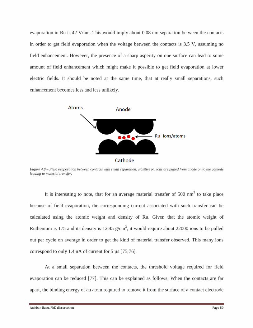
Anirban Basu, PhD dissertation Page 80
evaporation in Ru is 42 V/nm. This would imply about 0.08 nm separation between the contacts
in order to get field evaporation when the voltage between the contacts is 3.5 V, assuming no
field enhancement. However, the presence of a sharp asperity on one surface can lead to some
amount of field enhancement which might make it possible to get field evaporation at lower
electric fields. It should be noted at the same time, that at really small separations, such
enhancement becomes less and less unlikely.
Figure 4.8 – Field evaporation between contacts with small separation: Positive Ru ions are pulled from anode on to the cathode leading to material transfer.
It is interesting to note, that for an average material transfer of 500 nm3 to take place
because of field evaporation, the corresponding current associated with such transfer can be
calculated using the atomic weight and density of Ru. Given that the atomic weight of
Ruthenium is 175 and its density is 12.45 g/cm3, it would require about 22000 ions to be pulled
out per cycle on average in order to get the kind of material transfer observed. This many ions
correspond to only 1.4 nA of current for 5 µs [75,76].
At a small separation between the contacts, the threshold voltage required for field
evaporation can be reduced [77]. This can be explained as follows. When the contacts are far
apart, the binding energy of an atom required to remove it from the surface of a contact electrode

Anirban Basu, PhD dissertation Page 81
is large. Also, the energies associated with atom-anode and atom-cathode interaction as a
function of distance from the surface of an electrode do not overlap as shown in Figure 4.9.
Figure 4.9 – Atom-anode and atom-cathode interactions as a function of distance. The two interaction profiles do not overlap [77].
However, as the separation becomes smaller, these two interaction profiles start
overlapping which leads to a double-well structure. This results in a reduction of the binding
energy that an atom needs to overcome in order to move from one electrode to another. This can
be thought of as the field evaporation equivalent of direct tunneling in electrons where a small
contact separation can lead to electrons tunneling even at very low potentials. Figure 4.10 shows
this phenomenon.
Figure 4.10 – At small separations, the two interaction profiles to overlap. The sum of the two profiles has a double-well structure with a small activation barrier [77].

Anirban Basu, PhD dissertation Page 82
4.3. Polarity independent material transfer - bipolar hot switching tests
In Figure 4.11, material transfer is shown for the contact bump positive (anode), the contact
bump negative (cathode) and the contact bump alternating between cathode and anode on each
switching cycle (bipolar). Tests were conducted for both leading and trailing edge hot switching.
As shown here, we find that the material transfer is always from anode to cathode for unipolar
hot switching [66]. For bipolar hot switching the material transfer in the two directions nearly
cancels, resulting in far less net material transfer for the same number of cycles.
Note that ‘HS’ refers to hot switching. For all figures, ‘Anode’ refers to the contact bump
being the positive end of the electrode, and ‘Cathode’ refers to the contact bump being the
negative end of the electrode, while ‘Bipolar’ refers to the contact bump changing its polarity
each cycle i.e. one cycle of ‘Anode’ followed by one cycle of ‘Cathode’.

Anirban Basu, PhD dissertation Page 83
Figure 4.11 – Leading and trailing edge hot switching tests for comparing bipolar to unipolar contact damage – a) Leading edge hot switching with contact bump as anode for 106 cycles with 3.5 V hot switching voltage and 77.5 mA on-state current, b) Leading edge hot switching with contact bump as anode for 106 cycles with 3.5 V hot switching voltage and 77.5 mA on-state current, c) Leading edge bipolar hot switching for 106 cycles with 3.5 V hot switching voltage and 77.5 mA on-state current, d) Trailing edge hot switching with contact bump as anode for 106 cycles with 3.5 V hot switching voltage and 77.5 mA on-state current, e) Trailing edge hot switching with contact bump as cathode for 106 cycles with 3.5 V hot switching voltage and 77.5 mA on-state current, f) Trailing edge bipolar hot switching for 106 cycles with 3.5 V hot switching voltage and 77.5 mA on-state current
Subsequently, much longer tests were conducted with bipolar hot switching to see if a
smaller net transfer of material would occur despite the near cancellation because of the bipolar
testing. Two tests were conducted up to 40x106 cycles (one each for leading and trailing edge)
while one test lasting to 1.2x10⁸ cycles was performed and the contacts examined. Over the
course of the test it was noted that the contact resistance remained fairly low, showing that
despite the material transfer, the contacts were still able to sustain their performance. Figure 4.12
shows the images of the contacts after the tests were concluded, while Figure 4.13 shows the
electrical resistance of the contact over the course of the test that lasted 120 million cycles. The
corresponding image of the contact is shown in Figure 4.12(c).

Anirban Basu, PhD dissertation Page 84
Figure 4.12 – Long duration bipolar tests – a) Leading edge bipolar hot switching with 3.5 V hot switching voltage and 77.5 mA on-state current, b) Trailing edge bipolar hot switching with 3.5 V hot switching voltage and 77.5 mA on-state current, c) Trailing edge bipolar hot switching with 3.5 V hot switching voltage and 77.5 mA on-state current
Figure 4.13 – Contact resistance and contact force vs no of cycles for a long term bipolar hot switching test. Resistance is stable almost throughout the test and rises towards the end.
As shown in Figure 4.11, the net amount of material transfer in the bipolar case is much
less than for dc hot switching. This is not surprising since it is expected that material will

Anirban Basu, PhD dissertation Page 85
transfer from the anode to the cathode, which for the bipolar case means that material will
transfer back and forth between the two electrodes. It has earlier been discussed in Chapter 3
that the magnitude of material transfer was approximately independent of polarity of the force
sensor and pillar, implying that the amount of material transferred in the two directions will be
nearly equal.
Also shown in Figure 4.12 is that there is a net transfer of material in the bipolar case,
from the force sensor to the pillar. The observation that the volume of material transferred is
independent of the polarity of the force sensor and pillar might seem to imply that a mechanism,
different from the one responsible for the anode to cathode transfer of material, exists in the
bipolar case. On the other hand, the net transfer is small, so it could be a result of small
differences between the operations of the mechanism in the two directions. It is also possible that
any melted or evaporated asperity on either of the contacts might have a bias toward transferring
material to the cooler side, resulting in material transfer from bump to pillar as observed in the
bipolar experiments.
4.4. Hot switching damage at low current
If there is a critical value of current responsible for hot switching contact damage, then ideally
this damage can be reduced or ultimately completely eliminated if the current is limited to a
small value. However, while for trailing edge hot switching this may be true, at the leading edge,
the inherent capacitance of the system will limit how much we can reduce the current at a given
voltage. This is true whether the switch is part of a transmission line or a lumped element in a
circuit, or a test chip as in this work. At initial contact, the presence of such capacitance can

Anirban Basu, PhD dissertation Page 86
cause release of energy in the form of a current overshoot. In our test setup, a first order model
considering the SiO2 isolation layer between the device and handle sides of the chip predicts a
capacitance of approximately 35 pF. In order to analyze the effect of this added capacitance, a
SPICE model was used. With a switching frequency of 500 Hz, data showed the contact
resistance dropping from infinity to around 1 ohm within 10 µs. Simulating a switch with
behavior similar to a Ru-Ru contact in our test setup, the final SPICE model was set up as shown
in Fig 4.14.
Figure 4.14 – SPICE model of the equivalent circuit for the test setup considering the capacitance in the chip.
R3 shown above is the external in series resistor that was varied in order to analyze its
effect on circuit response. Using various values for this resistance, the following results were
found about the transient response in the circuit at the moment of contact.
R3
R4
50
0
V13.5
+-
+- S1VON = 2VOFF = 0V
V2
TD = 0TF = 10usPW = 50usPER = 100us
V1 = 0 TR = 10usV2 = 2
0
5 C3
4f FC41u
L1
125nH C6
35pF

Anirban Basu, PhD dissertation Page 87
a) b)
c) d)
e) f)
Figure 4.15 – Transient current response for an external resistance of a) 50 Ω, b) 500 Ω, c) 5 kΩ, d) 20 kΩ, e)1 MegΩ and f)10 Meg Ω. Note that for 1 and 10 MegΩ the second current spike is smaller than the first since the capacitance cannot charge up to its full value when RC constant becomes higher.
As shown in Figure 4.15, it was concluded from the SPICE model that a current
overshoot was not significant for an external in-series resistance of 1 kΩ and below with an
applied voltage of 3.5 V. From 10 kΩ or so, a current overshoot was observed which became
extremely significant (with respect to steady state current) at 100 kΩ and even up to 1 MegΩ.
Beyond that, for higher resistances of 10 MegΩ and above, only on the first cycle was a current
Anirban Basu, PhD dissertation Page 88
overshoot observed. From the second cycle onwards, the capacitance did not get enough time to
charge up so that it can discharge when the contacts come together. The current overshoot for 1
MegΩ could reach up to 125 µA which means if contact damage is caused by a current less than
that value, the mechanism would not be prevented by having a large resistance.
In a 50 Ω transmission line, however, from the simulation it is evident that the
capacitance does not have any significant effect and does not lead to any large current spike.
Therefore, typically, the capacitance does not have a role to play in the observed contact damage.
Experimentally, several tests were performed with external resistances of widely different
values from 50 Ω to 1 GigΩ. One important aspect of testing with external resistances that are of
high values (in the kΩ range and above), was that the effective resistance of the DAQ channel
measuring the contact voltage became comparable to the external resistance. This results in a
lower off-state hot switching voltage appearing across the contact and a higher voltage appearing
across the external resistance. The effective resistance of the DAQ channel is around 50 kΩ and
is a result of a tiny current being injected through the channel capacitance for measuring the
voltage. In order to ensure that the DAQ does not have an effect on the hot switching voltage
across the contact, the contact voltage was not measured when high resistance tests were
performed. In Figure 4.16, the images corresponding to contact damage at different values of
external resistance has been shown. It is clear that up to a resistance of 1 MegΩ, the contact
damage is significant. This correlates well with the simulation which predicts a current spike up
to an external resistance value of 1 MegΩ. The micrographs also suggest that the current that
causes contact damage is probably within 0.15 – 0.2 mA but not too low since 10 MegΩ does not
lead to much damage at all.

Anirban Basu, PhD dissertation Page 89
a) b)
c) d)
e) f)
Figure 4.16 – Contact damage with 3.5 V hot switching voltage after 106 cycles for leading edge hot switched tests with different external resistances: a) Leading edge hot switching with 3.5 V hot switching voltage, 3.9 V on state voltage, 50 Ω external resistance and contact bump as anode, b) Leading edge hot switching with 3.5 V hot switching voltage, 3.9 V on state voltage, 500 Ω external resistance and contact bump as anode, c) Leading edge hot switching with 3.5 V hot switching voltage, 3.9 V on state voltage, 5k Ω external resistance and contact bump as anode, d) Leading edge hot switching with 3.5 V hot switching voltage, 3.9 V on state voltage, 20 k Ω external resistance and contact bump as anode, e) Leading edge hot switching with 3.5 V hot switching voltage, 3.9 V on state voltage, 1 Meg Ω external resistance and contact bump as anode, f) Leading edge hot switching with 3.5 V hot switching voltage, 3.9 V on state voltage, 10 Meg Ω external resistance and contact bump as anode.
Figure 4.16 shows the contact damage with different external resistances. The observed
trend suggests that it is possible that the contact damage may be related to the capacitance in the

Anirban Basu, PhD dissertation Page 90
system for high impedance tests. It also indicates that the magnitude of current associated with
this damage is in the order of 100 µA or so given that a 1 MegΩ resistance shows significant
damage as well. For extremely high R such as 10 MegΩ, the capacitance does not charge up to
allow current flow when contact occurs. For external resistances less than, however, 20 kΩ, the
capacitance does not have a significant role to play. In most RF circuits, considering a
characteristic impedance of 50 Ω, the capacitance should not have an effect on the contact
damage.
4.5. Slow approach and separation of contacts
Tests were performed to study the effect of slow approach and separation of contacts at a hot
switching voltage of 3.5 V and 5 V. The tests were run for about 40-45 minutes at an
approach/separation rate of 8.8 nm/s. For these tests, the actuation voltage applied to the piezo-
actuator was ramped up from 0 to 50 V in 125s. Voltage was applied separately with a source
measure unit. Figures 4.17 – 4.19 show the results that emerged from these tests.
a) b)
Figure 4.17 – Leading edge hot switching tests at 3.5 V hot switching voltage, 50 Ω resistor, with contacts approached at 8.8 nm/s: a) Contact bump is anode, b) Contact bump is cathode
Figure 4.17 represents tests where a hot switching voltage was applied only at the leading
edge. Here, the hot switching voltage applied is 3.5 V with an external resistance of 50 Ω. With

Anirban Basu, PhD dissertation Page 91
an approach rate of 8.8 nm/s, 40 – 50 switching cycles were performed. On examining the
contacts after cycling, no observable damage to these contacts was detected either for the case
where the contact bump was the anode, or when it was the cathode. By reducing the ramping rate
by a factor of 500,000, effectively the contacts spend time in close proximity for an amount of
time that is increased by the same factor. Thus, the damage from 40 – 50 cycles should be
equivalent to 20,000,000 cycles at the normal switching speed (when ramp rate is 4400 µm/s)
unless contact damage occurs exactly at the point of contact or just before in which case the
amount of time spent in proximity becomes irrelevant. The material transfer under these
conditions is insignificant which tends to point towards a mechanism that is independent of the
time spent in close proximity.
Figure 4.18 shows the result of tests done under the same hot switching voltage of 3.5 V
and ramp rate of 8.8 nm/s, but this time the voltage was applied at the trailing edge while the
contacts separated. The contacts were again cycled 40 – 50 times and for different polarities.
Trailing edge tests were also performed at a hot switching voltage of 5.0 V as shown in Figure
4.19. Surprisingly, the results for the two hot switching voltages were quite different.

Anirban Basu, PhD dissertation Page 92
a) b)
c)
Figure 4.18 – Trailing edge hot switching tests at 3.5 V hot switching voltage, 50 Ω resistor, with contacts separated at 8.8 nm/s: a) Contact bump is anode, b) Contact bump is cathode, c) Contact bump is cathode
a) b)
c)
Figure 4.19– Trailing edge hot switching tests at 3.5 V hot switching voltage, 50 Ω resistor, with contacts separated at 8.8 nm/s: a) Contact bump is anode, b) Contact bump is cathode, c) Contact bump is cathode
From Figures 4.18 and 4.19, it can be concluded that the material transferred for slow
trailing edge hot switching is polarity dependent when the voltage applied is 3.5 V. However,

Anirban Basu, PhD dissertation Page 93
between 3.5 V to 5.0 V there is a change in the dominant mechanism for material transfer. At 5.0
V, irrespective of the polarity of the material transfer, material is always transferred away from
the contact bump. Also, at 3.5 V, the material transferred away from the contact bump when the
contact bump is the anode looks to be greater than the material transferred on to the bump when
it is the cathode. This appears to suggest that there are two mechanisms occurring simultaneously
which either reinforce or oppose each other. One mechanism is possibly related to the
temperature difference between the contact and the pillar purely on account of the mass
difference. The other is a polarity dependent mechanism which could be electromigration or the
Thomson effect
While separating, the electrodes stayed together for a time beyond the neutral point of the
force structure (where the contact force is zero). Therefore, the pillar had to be pulled down
below this neutral point in order to let the electrodes completely separate. Although this behavior
was initially thought to be due to adhesion, further investigation proved joule heating at the
contact causes the force structure to bend towards the pillar causing them to stay in contact
longer [63]. This behavior would let the trailing edge hot switching mechanism operate longer
than it otherwise would, particularly if the material transfer occurs when a metal bridge is formed
and not after the contacts separate. Therefore, it would not be fair to compare leading edge hot
switching results at this rate with the trailing edge since the differences would be, at least
partially, an artifact of the testing system. However, it is valid to compare the results of 3.5 V hot
switching with 5.0 V hot switching which demonstrated a change in the way conflicting damage
mechanisms operate for trailing edge.
Yet another set of experiments for trailing edge hot switching was conducted where the
contacts were not allowed to come apart. Here instead, the contacts were allowed to slowly
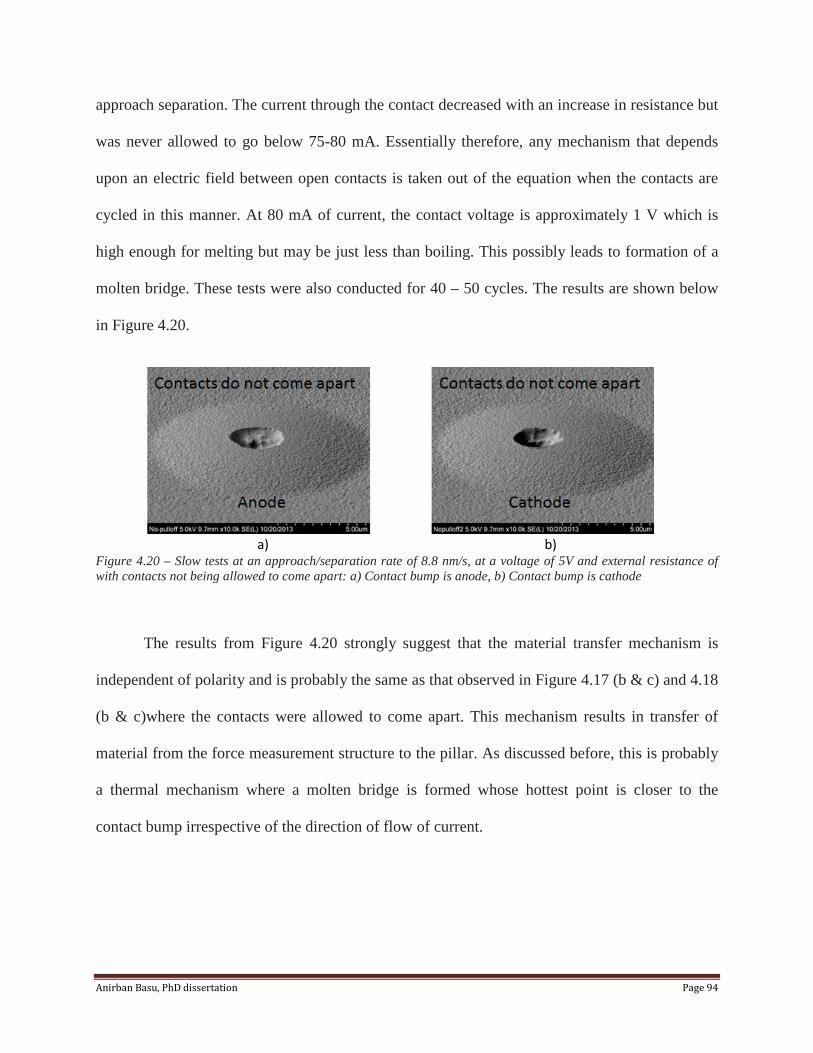
Anirban Basu, PhD dissertation Page 94
approach separation. The current through the contact decreased with an increase in resistance but
was never allowed to go below 75-80 mA. Essentially therefore, any mechanism that depends
upon an electric field between open contacts is taken out of the equation when the contacts are
cycled in this manner. At 80 mA of current, the contact voltage is approximately 1 V which is
high enough for melting but may be just less than boiling. This possibly leads to formation of a
molten bridge. These tests were also conducted for 40 – 50 cycles. The results are shown below
in Figure 4.20.
a) b)
Figure 4.20 – Slow tests at an approach/separation rate of 8.8 nm/s, at a voltage of 5V and external resistance of with contacts not being allowed to come apart: a) Contact bump is anode, b) Contact bump is cathode
The results from Figure 4.20 strongly suggest that the material transfer mechanism is
independent of polarity and is probably the same as that observed in Figure 4.17 (b & c) and 4.18
(b & c)where the contacts were allowed to come apart. This mechanism results in transfer of
material from the force measurement structure to the pillar. As discussed before, this is probably
a thermal mechanism where a molten bridge is formed whose hottest point is closer to the
contact bump irrespective of the direction of flow of current.

Anirban Basu, PhD dissertation Page 95
4.6. Thermal effects and electromigration
Thermal effects are always associated with any electrical contact. At a high enough contact
voltage melting and evaporation can occur. Further, the resultant metal vapor can ionize leading
to material transfer as the positive ions are attracted towards the cathode. Also, in the event of
formation of a metal bridge between the contacts, the bridge can also rupture at its hottest point
which can be determined by joule heating or Thomson effect. Since the rupture point will be
biased towards the hotter electrode, this will lead to material transfer as well.
The theoretical value for melting voltage of a contact depends on its thermal
conductivity, electrical resistivity and melting temperature [32,78]. The relationship between
contact voltage and temperature has been discussed extensively and is shown to be [32,79,80]:
𝑉2 = 8 𝜆𝜌𝑑𝑇
𝑇𝑚
𝑇0
λ and ρ are the thermal conductivity and electrical resistivity respectively. Tm is the
temperature at the contact spot while T0 is the temperature at a location that is far away from the
contact spot (ambient temperature). Also, the Wiedemann-Franz law states that the product λρ is
proportional to absolute temperature T. If the proportionality constant is L or Lorentz number
given by [81], then
𝜆𝜌 = 𝐿𝑇
The final relationship between temperature and voltage is [32]:
𝑇𝑚2 = 𝑇02 +𝑉2
4𝐿

Anirban Basu, PhD dissertation Page 96
The temperature of the contact spot varies as the square of the voltage which indicates
that the temperature can quickly reach the boiling point. The boiling point of Ru is 4423 K and
its melting point is around 2607 K. Since the melting voltage of Ru is around 0.8 V which
indicates that the boiling voltage is around 1.4 V.
Melting can occur for both leading and trailing edge hot switching. However, for leading
edge hot switching, melting will lead to contacts sinking into each other thereby increasing the
contact area which leads to lower contact resistance and lower voltage across the contact. At the
trailing edge, we can have one of two things. One possibility is that the contacts can pull apart
completely after initial adhesion. A second possibility is that as the contact area gets smaller the
contact voltage approaches the melting voltage. At this stage, a metal bridge will be formed
while the contacts continue to pull apart. This causes the temperature of the bridge to continue
increasing beyond the melting point. When the temperature is high enough, the molten bridge
that was formed can evaporate and ionize leading to the positively charged ions getting attracted
towards the cathode thereby resulting in material transfer from the anode on to the cathode.
For ionization of a vapor of Ru metal, a high temperature is required. The relationship
between ionization fraction of volume of vapor to its temperature is given by Saha equation:
𝑁𝑖+1
𝑁𝑖 =𝑍𝑖+1
𝑍𝑖2
𝑛𝑒ℎ3(2𝜋𝑚𝑒𝑘𝑇)3 2 𝑒
𝜒𝑖𝑘𝑇
Here, Ni refers to the number of atoms in the ith ionization state of the atom, Zi refers to
the partition function for the ith ionization state, me is the mass of an electron, h is Planck’s
constant, ne is the electron number density, k is Boltzmann’s constant, T is the absolute
temperature of the system, while χi is the ionization energy in eV. Using this equation for

Anirban Basu, PhD dissertation Page 97
Hydrogen, we get an ionization fraction of 0.8 at a temperature of 10,000 K [82]. This is much
lower than the temperature that would be predicted by equating ionization energy with kinetic
energy of a molecule (32𝑘𝑇) at a given temperature. For Hydrogen, this would have given an
ionization temperature of 163,200 K. For Ruthenium, equating ionization energy with kinetic
energy would give an ionization temperature of 88,272 K. Scaling this temperature down by the
same factor as for Hydrogen would give us an approximate ionization temperature of 5,000 K
which is only slightly greater than the boiling temperature. The probability of a metal vapor of
Ruthenium to be ionized, leading to material transfer towards the cathode, is therefore extremely
high.
Electromigration also cannot be discounted in the context of hot switching in
microcontacts. Electromigration refers to mass transport in a conductor that occurs as a result of
high current densities [47,83]. At current densities above 104 A/mm2, electromigration can
become significant. If we consider a current of 75 mA, then the radius of the bridge needs to be 1
µm. For the microcontacts being tested here, the contact spot(s), just before opening, is an order
of magnitude (or more) smaller than this thereby giving an even higher current density and hence
the probability of electromigration occurring increases by an order or more.
Due to the electric field of a conductor, electrons are pulled towards the cathode, while
the ions are pulled towards the anode. However, the energy transferred to the ions from collision
with electrons as well as the electrostatic pull of the electrons will result in the ions also
experiencing a pull towards to cathode. Thus, there are two opposing forces acting on the ions.
The drift velocity of the ions due to electromigration is given in literature by the following
equation [47,83]:

Anirban Basu, PhD dissertation Page 98
𝑉 = 𝐽𝑒𝑍∗𝜌𝐷/𝐾𝑇
Here, V is the velocity of ion transport; Z*e is the effective charge in the ion taking into
account electrostatic force due to applied electric field, as well as the influence of the electrons; ρ
is the resistivity of the contact material, D is the diffusion coefficient of the ions, K is
Boltzmann’s constant and T is the absolute temperature of the contact spot.
Usually, electromigration in metals occurs in the direction of flow of electrons i.e.
cathode to anode which implies Z* is < 0. In a fluid, however, since the ions have additional
thermal energy, they may be prone to move towards the cathode. Anode to cathode material
transfer has been reported in Al, Ag, In and other metals, particularly in the molten state
[47,84,85].
The flow of current in an electrical contact leads to joule heating of the contacts. At the
time of contact opening, if a metal bridge is formed and the temperature does not reach
evaporation point, then the bridge will eventually break at its hottest point. Due to the thermal
asymmetry between the two electrodes, this hottest point will be biased away from the pillar,
which on account of its greater mass is the better heat sink [63]. As a result of this, there will be
asymmetric transfer of material towards the pillar irrespective of the polarity of the applied
voltage. This effect, therefore, will be polarity independent and will always lead to material
transfer away from the contact bump. It is possible that the material transfer observed with
bipolar hot switching is due to this mechanism. The thermal effect also explains why the material
is always transferred from the contact bump during the slow tests at 5 V, and in case of 3.5 V
there is less material transferred on to the contact bump when it is the cathode than what is
transferred away from it when it is anode.

Anirban Basu, PhD dissertation Page 99
The Thomson effect is another thermal mechanism that should be discussed in the
context of material transfer. In an electrical contact, a temperature gradient will occur as a result
of the voltage across the contact and the flow of current [32,86] in addition to the temperature
gradient due to Joule heating discussed earlier. The temperature gradient may be from anode to
cathode or the other way around depending on the sign of the Thomson coefficient. A positive
Thomson coefficient leads to the cathode being hotter. This is exhibited in metals such as Cu and
Ag. A negative Thomson effect, exhibited in Pt, Ni and Bi, leads to the anode being hotter [87].
However, when Pt was investigated, it was found that depending on its state (solid or liquid), its
Thomson coefficient can change signs [32]. While data pertaining to Thomson coefficient for Ru
is not yet available, some of the results obtained in the course of this thesis can be discussed in
with the Thomson effect in mind. In the event of a molten bridge being formed while the
contacts start to separate, the molten bridge will break at the point of the highest temperature and
therefore will lead to material being transferred from the hotter to the cooler electrode.
4.7. Summary of hot switching damage mechanisms
From the results and discussion in chapters 3 and 4, it can be concluded that hot switching
damage in microswitch contacts can be due to a number of different mechanisms. Among the
likely mechanisms are – a) Mechanical transfer through adhesion, cold welding or softening of
contact as observed in low voltage hot switching; b) Field Evaporation; c) Field emission leading
to heating, melting and evaporation; d) Electromigration with and without melting which can
also manifest itself through surface diffusion; e) Ionization of metal vapor; f) Formation of metal
bridge where Thomson effect and thermal asymmetry can cause the hottest point of the bridge to

Anirban Basu, PhD dissertation Page 100
be biased towards one of the electrodes. Having discussed each of these mechanisms separately,
it is pertinent to look at a hot switching cycle holistically and understand how the mechanisms
are likely to operate in the course of a cycle.
4.7.1. Hot switching mechanisms at the leading edge
For leading edge hot switching, as the contacts approach each other, field emission through
either Fowler Nordheim tunneling (for voltages above the work function) or direct tunneling (for
voltages below the work function) will occur. Depending on the material properties of the
contact as well as the tunneling current, some amount of melting or even evaporation might
occur due to field emission. Both for Fowler Nordheim tunneling through a triangular barrier as
well as direct tunneling through a trapezoidal barrier, a separation on the order of a few Å is
necessary in order to achieve a current level of approximately 1 µA considering a contact area of
around 5 nm2. At smaller separations, the current increases exponentially and can reach
approximately 1 mA at 1 Å [68] which could lead to evaporation. Material transfer due to this
mechanism will be from anode to cathode.
Electric field between the contacts can cause surface diffusion of the ions towards the
apex of the anode. Furthermore, if tunneling current causes heating at the anode, this can lead to
melting which can further promote surface diffusion towards the apex of the contact. The process
of surface diffusion is similar to electromigration where ions are pulled by the electric field
between the contacts. Ultimately a liquid cone may form at this tip which can be long enough to
touch the other electrode thereby depositing material on to it. This was speculated to be a
material transfer mechanism in AFM/STM tips in [77].

Anirban Basu, PhD dissertation Page 101
Field evaporation might also become prominent at such small separations leading to
material transfer once again from anode to cathode. Conventional field evaporation theory such
as that presented in [88], considers a threshold electric field for evaporation, using first principles
such as the image-hump model, at which atoms are able to break the barrier potential between
them and the contact surface. However, at small separations (4 – 6 Å), when the interaction
profiles of the anode and the cathode combine, the atoms can essentially tunnel from one surface
to another at smaller electric fields which can be 30-40% lower than the value at large
separations [77]. Thus, if the usual electric field required for evaporation for Ru is 4.1 V/Å, then
at small separations, it can be approximately 2.5 V/Å. At less than 4 Å, the required electric field
can be less than 50% of the 4.1 V/Å value. Therefore, for a voltage of 3.5 V as applied to most of
the contacts tested as part of this work, the required separation for field evaporation can be
approximately 1.5 Å. This phenomenon leading to material transfer at low voltages is also
observed in STM tips when the sample is held close to it.
At the moment of initial contact, when the contact voltage is highest, melting or
potentially boiling of the contact surface can take place leading to formation of a metal cloud
which, depending on its temperature may get ionized thus leading to material transport towards
the cathode where the ions will get attracted. Electromigration and surface diffusion, as a
consequence of the high current density can also occur at this point. If the contact voltage is large
enough to melt but not cause evaporation, it is likely that the contacts will ‘sink’ into each other
thereby causing an increase in contact area and lower resistance thereby quickly bringing down
the contact voltage [32].

Anirban Basu, PhD dissertation Page 102
4.7.2. Hot switching mechanisms at the trailing edge
At the time of contact opening, the sequence of events could be different, although some or all of
the same mechanisms might still be active. When the contacts start separating, the contact
voltage starts to rise as the resistance increases. At the melting voltage, which is 0.8 V for Ru, a
molten bridge will form between the contacts. The hottest point of this molten bridge will
determine the point at which this bridge will break. The hottest point can depend upon several
factors. If we consider joule heating, the contact bump will be the hotter of the two electrodes on
account of the fact that the pillar has more mass and is a better heat sink. This will shift the
hottest point of the molten metal bridge towards the anode. However, other mechanisms are also
active. One is the Thomson effect. Depending on the sign of the Thomson coefficient for the
contact material when it is at its molten state, the Thomson effect will lead to a thermal gradient
from either anode to cathode or the other way around [89]. While data on the Thomson
coefficient of Ruthenium is not available, it is possible that it will cause the hottest point to shift
toward the anode [32] causing material transfer from anode to cathode.
Another polarity dependent mechanism leading to material transfer is electromigration.
While electromigration is generally associated with solids, it can also be present in a molten
bridge [47,86]. In a molten bridge, electron diffusion can lead to ion transport which will
ultimately cause the molten bridge to break while transporting material to one of the electrodes.
Although conventionally electromigration leads to material transfer from the anode to the
cathode, the opposite has also been observed for metals such as Ag.
It was found that at a very slow separation rate of 8.8 nm/s, a voltage of 5 V and an
external resistance of 50 Ω, material transfer always occurred from contact bump to pillar

Anirban Basu, PhD dissertation Page 103
irrespective of which of these was the anode. This would imply that the thermal effect took
precedence over any polarity dependent effect that might also be present. At 3.5 V and an
external impedance of 50 Ω, however, material transfer was polarity dependent and thus the
thermal effects were effectively offset by the polarity dependent mechanism which could be
Thomson effect or electromigration. It was noted that although material transferred in both
directions, but there was much more from the bump to pillar, implying that the two mechanisms
were active simultaneously.
While the role of the molten bridge may be important for trailing edge hot switching, the
other field dependent mechanisms can also occur once the molten bridge has broken. These
include field emission and field evaporation. When the bridge ruptures at its hottest point, the
material on either end of the rupture point will re-solidify. Subsequently, field emission and field
evaporation can occur between the resultant asperities for a short duration before the separation
between the contacts increase further.
Furthermore, there is also the possibility of a portion of the molten bridge evaporating
when the contact voltage is close to boiling voltage, which for Ru can be estimated to be around
1.2 V given that contact temperature is proportional to the square of the contact voltage and that
the melting voltage of Ru is 0.8 V. Boiling of the bridge can lead to formation of a metal vapor
which could get ionized at a sufficiently high temperature that would lead to material being
deposited on the cathode. This mechanism is similar to what can happen at the leading edge.
It was also observed that at an external impedance of 5 kΩ, trailing edge hot switching
gave rise to less contact damage than leading edge hot switching. This can perhaps be explained
by the fact that at the trailing edge when the melting voltage is reached, the contact resistance

Anirban Basu, PhD dissertation Page 104
would be about 1 kΩ if the total applied voltage is 3.5V. The resultant contact area under the
circumstances would be about 0.36 Å (if resistivity of Ru is 7.1 µΩ-cm and = 𝜌2𝑎
) which is less
than an atom’s size.
4.7.3. Evidence of Multiple mechanisms
The presence of multiple mechanisms operating simultaneously, leading to hot switching
damage, is clear from various results obtained in this work. For instance, at a hot switching
voltage of 0.5 V, material is displaced due to softening and as such does not lead to transfer of
material. The presence of a polarity dependent mechanism together with a polarity independent
thermal mechanism is clear from the results of bipolar hot switching as well as those where
contacts are cycled extremely slowly. Also, at the leading edge, contacts can weld together due
to high temperature and then when they come apart, this can cause material to be scattered. At
the trailing edge, the material transfer and contact erosion appears a lot smoother possibly due to
the formation of an intermediate molten bridge.
The results discussed in Chapters 3 and 4, can be used as evidence for presence of
multiple mechanisms during hot switching. While the evidence available is complex, a careful
analysis can help relate the data already presented with possible mechanisms. Given below are
two tables – one showing how different test results can be associated with certain mechanisms,
and another showing how some of the possible mechanisms could be associated with images of
the damaged contacts.
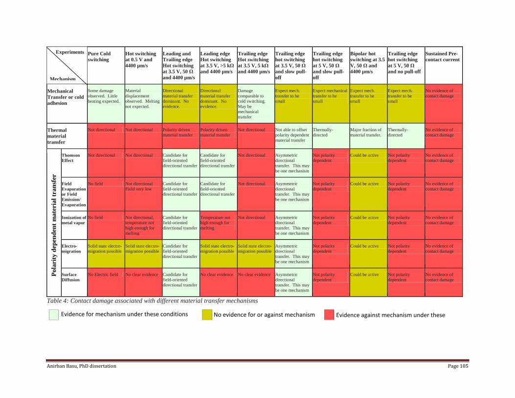
Anirban Basu, PhD dissertation Page 105
Pure Cold switching
Hot switching at 0.5 V and 4400 µm/s
Leading and Trailing edge Hot switching at 3.5 V, 50 Ω and 4400 µm/s
Leading edge Hot switching at 3.5 V, >5 kΩ and 4400 µm/s
Trailing edge Hot switching at 3.5 V, 5 kΩ and 4400 µm/s
Trailing edge hot switching at 3.5 V, 50 Ω and slow pull-off
Trailing edge hot switching at 5 V, 50 Ω and slow pull-off
Bipolar hot switching at 3.5 V, 50 Ω and 4400 µm/s
Trailing edge hot switching at 5 V, 50 Ω and no pull-off
Sustained Pre-contact current
Mechanical Transfer or cold adhesion
Some damage observed. Little heating expected.
Material displacement observed. Melting not expected.
Directional material transfer dominant. No evidence.
Directional material transfer dominant. No evidence.
Damage comparable to cold switching. May be mechanical transfer
Expect mech. transfer to be small
Expect mechanical transfer to be small
Expect mech. transfer to be small
Expect mech. transfer to be small
No evidence of contact damage
Thermal material transfer
Not directional Not directional Polarity driven material transfer
Polarity driven material transfer
Not directional Not able to offset polarity dependent material transfer
Thermally-directed
Major fraction of material transfer.
Thermally-directed
No evidence of contact damage
Thomson Effect
Not directional Not directional Candidate for field-oriented directional transfer
Candidate for field-oriented directional transfer
Not directional Asymmetric directional transfer. This may be one mechanism
Not polarity dependent
Could be active
Not polarity dependent
No evidence of contact damage
Field Evaporation or Field Emission/ Evaporation
No field Not directional Field very low
Candidate for field-oriented directional transfer
Candidate for field-oriented directional transfer
Not directional Asymmetric directional transfer. This may be one mechanism
Not polarity dependent
Could be active Not polarity dependent
No evidence of contact damage
Ionization of metal vapor
No field Not directional, temperature not high enough for melting
Candidate for field-oriented directional transfer
Temperature not high enough for melting
Not directional Asymmetric directional transfer. This may be one mechanism
Not polarity dependent
Could be active Not polarity dependent
No evidence of contact damage
Electro-migration
Solid state electro-migration possible
Solid state electro-migration possible
Candidate for field-oriented directional transfer
Solid state electro-migration possible
Solid state electro-migration possible
Asymmetric directional transfer. This may be one mechanism
Not polarity dependent
Could be active Not polarity dependent
No evidence of contact damage
Surface Diffusion
No Electric field No clear evidence Candidate for field-oriented directional transfer
No clear evidence No clear evidence Asymmetric directional transfer. This may be one mechanism
Not polarity dependent
Could be active Not polarity dependent
No evidence of contact damage
Table 4: Contact damage associated with different material transfer mechanisms
Evidence for mechanism under these conditions No evidence for or against mechanism Evidence against mechanism under these
Pola
rity
dep
ende
nt m
ater
ial t
rans
fer
Mechanism
Experiments

Anirban Basu, PhD dissertation Page 106
Mechanism Figure number(s)
Mechanical transfer, cold adhesion Figures 3.4 to 3.7 (0.25 V and 0.5 V tests)
Field Evaporation Figures 3.9, 3.10, 3.12 and 4.16
Field emission leading to heating, melting and evaporation
Figures 3.9, 3.10, 3.12 and 4.16
Electromigration (molten or solid) and surface diffusion
Figures 3.11, 4.18, 4.19 and 4.20
Ionization of metal vapor Figures 3.9, 3.10 and 3.12
Thermal bias due to Thomson effect Figures 4.18, 4.19 and 4.20
Thermal asymmetry due to geometry Figures 4.12 and 4.20
Table 5: Figures associated with different material transfer mechanisms
In summary, then, it is important to note that contact damage due to hot switching can
occur due to a number of different mechanisms. The results of hot switching tests at different
voltages demonstrate the presence of multiple contact damage mechanisms. The mechanisms
operate at very short separations or when the contacts are just touching. While there are some
similarities between leading and trailing edge hot switching (similar amount of material transfer
at a switching speed of 4400 µm/s), there could be effects which are present in one and not the
other. It is also noted that pre-contact currents, observed in ‘dirty’ contacts [39,40,76] do not
cause material transfer.

Anirban Basu, PhD dissertation Page 107
Chapter 5 - Hot switching phenomena not leading to contact damage
5.1. Observation and analysis of large current spikes
To monitor in detail the current behavior before closing and after opening of the contact, a 50 Ω
external resistor was placed in series with the contact in addition to the built-in testing system 5
Ω series resistor, as shown in Figure 5.1(a). The voltage across this added resistor was measured
with an oscilloscope with an acquisition rate of (500 MS/s); current in the circuit was calculated
using Ohm’s law.
Several current monitoring tests were conducted at various applied voltages and
frequencies for both leading edge and trailing edge hot switching. Figure 5.1 illustrates an
example of typical current behavior observed before closing and after opening of a contact
cycled at 500 Hz with 55 Ω total series resistance and hot switching potential 3 V. There are
several properties of note presented in this figure. First, the magnitude and anatomy of the spikes
is remarkably similar. It is important to note that the plotted data came from two different cycles
and that not all the current spikes observed look identical to the ones presented; there was some
variation in magnitude, duration, and periodicity observed. The similarities in the current spikes
suggest that the same underlying mechanism is causing both.

Anirban Basu, PhD dissertation Page 108
Figure 5.1 (a) Schematic of test circuit with external resistor (b) Current spikes measured via the external resister before closing and after opening in a contact cycled at 500 Hz with 3.00VHot and 55 Ω of total series resistance
It was initially conjectured that these spikes are related to the observed material transfer
as well. However, these spikes stopped appearing once the coaxial cable connected across the
contact, for measuring the contact voltage with an oscilloscope, was disconnected. This indicated
that the spikes could have been a result of the capacitance in the coaxial cable interacting with
asperities on the contact surfaces blowing them out [75]. Contacts were tested up to 500,000
cycles after removing the coaxial cable and the material transfer compared qualitatively with
contacts cycled the same number of times with the cable connected. The amount of material
transfer appeared to be the same in both cases, indicating that the larger spikes did not contribute
to the anode-to-cathode material transfer.
Figure 5.1 shown earlier tells us about the observed large current spikes just before
closure and immediately after contacts open. The effect of circuit parasitics, which have been

Anirban Basu, PhD dissertation Page 109
known to cause spikes in currents, needed to be studied closely to examine their role in contact
damage. A few basic experiments were done to better understand the spikes.
Figure 5.2 – Realistic circuit for the test setup
The figure above (Figure 5.2) is the effective circuit for the test setup. The circuit shows
the parasitic inductance and capacitance in the interconnections. Between the switch and the
external 50 Ω resistor though, there is no parasitic because of the use of a transmission line
terminator for the co-ax cable.
The first modification done to this circuit was removing the DAQ that was reading the
voltage across switch. Since the DAQ can introduce currents (although not as high as the spikes
seen), this was seen as a logical first step. It was then observed that the spikes almost
disappeared. They are still occasionally seen but even those are of much shorter duration than
that noticed earlier with the DAQ on.

Anirban Basu, PhD dissertation Page 110
Figure 5.3 – Test setup with DAQ disconnected
Figure 5.3 above shows circuit without the DAQ being connected across the contact.
Figure 5.4 shows the nature of the leading and trailing edge behavior of the current following the
removal of the DAQ. Note that at the trailing edge the current level is lower. This is seen often
and is associated with increase in resistance when the contacts are coming apart.
Figure 5.4 – Current spikes in the absence of a DAQ across the contact

Anirban Basu, PhD dissertation Page 111
Following the results observed in the figure above, a few more tests were performed. The
co-axial cable used for measuring contact voltage was now connected to the contact without the
other end being connected to the DAQ break-out box. This was done to test the effect of the
parasitic capacitance to ground of the co-axial cable. It was observed that the spikes are now
back. By calculating the approximate capacitance of the cable alone to be around 1 nF, the author
decided to connect just a 1 nF capacitor in parallel with the contact. This caused the spikes to
reappear. The final results can be summarized in Figure 5.5 below.
a)
b)

Anirban Basu, PhD dissertation Page 112
c)
Figure 5.5 – a) Circuit with 1 nF capacitor, b) Circuit with co-axial cable parallel with contact, c) Current spikes corresponding to the two circuits respectively
To check if the spikes themselves were responsible for the material transfer, two different
contacts were cycled up to 500,000 cycles with and without the DAQ being connected. The
images, shown in Figure 5.6, revealed that in both cases the material transfer was comparable
thereby definitively proving that the spikes had nothing to do with material transfer. However,
keeping in mind the fact the spikes are not regular and thus cannot be related to any mechanical
phenomena such as resonant frequency of the structures, and also the fact that at lower voltages
these spikes are not observed, it is clear that the spikes are being triggered by circumstances
related to hot switching even if they are not responsible for material transfer. The images of the
cycled contacts under the two different conditions are shown below:

Anirban Basu, PhD dissertation Page 113
a) b)
Figure 5.6 a) Contact after 500,000 cycles with no DAQ connected, b) Contact after 500,000 cycles with DAQ in parallel
5.2. Current transients in RF hot switching
The source and load capacitance in an RF system can be estimated by using a typical value of
standing wave ratio. These capacitances, along with the effective capacitance of the RF MEMS
switch, can cause current transients at the time of closing of the contact. An analysis of these
current transients was necessary to conclude if they can have an effect on contact damage.
Although no experimental work has been done so far under RF conditions, an analytical study of
such a system was necessary for an insight into its behavior.
Figure 5.7 shows the effective circuit under RF conditions.

Anirban Basu, PhD dissertation Page 114
Figure 5.7 – Equivalent circuit for a simple RF system with inductance and capacitance of the switch taken into consideration
The values of source and load capacitances as well as the effective inductance and
capacitance of the switch were used from Gabriel Rebeiz’s textbook for RF MEMS [3] and
correspond to values that lead to a Standing wave ratio observed in a realistic RF circuit. As an
example, the switch characteristics used for simulating the switch resistance in the circuit were
derived from data available on the NEU-Radant MEMS switch.
Given the Force vs Resistance data and the Force vs time for a typical switch, the
resistance vs time curve was derived as shown in Figure 5.8. This curve can be simulated on
Spice by having several ideal switches in parallel. After this simulation, the current transients are
studied for various values of dF/dt i.e. the switch closure rate. Expectedly, the switch closure rate
has a significant effect on the magnitude of the current transients. Another factor that influences
the magnitude of the current transients is the phase of the input RF signal at which the switch
closes. Figure 5.9 shows the current transient at different values of dF/dt.

Anirban Basu, PhD dissertation Page 115
Figure 5.8 – Force vs time, Force vs Resistance and Resistance vs time for contacts with different material
Figure 5.9 – Current transient in an RF microswitch vs dF/dt of the switch – the black vertical line represents the dF/dt of a standard
The data above tells us that at realistic values of dF/dt, only Au-Au contacts show any
significant current transient which implies that these high values of current transients are not
available for causing damage in RF circuits.

Anirban Basu, PhD dissertation Page 116
Another somewhat pertinent result was obtained through this circuit model. It was
observed, as shown in Figure 5.10 that the current transient in an RF system depends on phase
angle at which contact is made.
Figure 5.10 – Current transient vs phase angle at which contact is closed – it should be noted that the current overshoot as a function of phase is plotted at an unrealistic value of dF/dt so as to amplify its magnitude
For Ru-Ru contacts the current transients are very low for all phase angles and all values
of dF/dt; Also, the plot for current transient against phase angle was with respect to the highest
value of current transient at a dF/dt of 100x103 N/s which is unrealistic for these switches.
Anirban Basu, PhD dissertation Page 117
Chapter 6 - Conclusion and future work
In this thesis, contact damage in Ruthenium-on-Ruthenium microcontacts as a result of hot
switching has been discussed. While it was known that hot switching leads to a reduction in the
lifetime of microswitch contacts, the damage mechanisms causing it was poorly understood.
Using an AFM-based test setup a large number of experiments were performed, under different
hot switching conditions, to observe and characterize these mechanisms. For these tests, a
clamped-clamped beam structure with a bump at its center was used as one side of the contact.
The other side was a pillar which was placed on a piezoactuator whose expansion and
contraction caused the contacts to meet and then come apart thereby replicating switching cycles
in a microswitch.
Material transfer, leading to removal of contact material from one side of the contact,
subsequently causing contact resistance to increase, was found to be the primary cause for
contact failure in DC hot switching. Both leading and trailing edge hot switching, at a hot
switching voltage of 3.5 V, were found to quantitatively lead to similar amounts of material
transfer when an external resistance of 50 Ω was used in series with the contact, at a cycling
frequency of 500 Hz. However, with a 5 kΩ resistor, leading edge hot switching was found to be
much more damaging than trailing edge hot switching. Material transfer in bipolar hot switching
was found to be several orders of magnitude lower than DC hot switching. It was observed that
some amount of material transfer is still unavoidable with bipolar hot switching at a cycling
frequency of 500 Hz and a hot switching voltage and external resistance of 3.5 V and 50 Ω
respectively. The mechanism leading to such material transfer was speculated to be thermal since
any field dependent mechanism should be effectively neutralized. Both leading and trailing edge
bipolar hot switching was found to lead to material transfer away from the contact bump. The

Anirban Basu, PhD dissertation Page 118
contact resistance for a bipolar hot switched test, however, was found to remain low for the
entire course of the test up to 120 million cycles.
Multiple mechanisms were found to operate and lead to contact damage during both
leading and trailing edge hot switching. At low hot switching voltages, below 2.0 V, it was found
that there was no regular pattern to the direction in which material was transferred with respect to
the polarity of the applied voltage. At 0.5 V, it was found that there was a significant increase in
contact damage compared to cold switching or at 0.25 V, although this damage also was not
polarity dependent and may not lead to contact erosion but rather its displacement. From 0.5 V to
1.0 V, however, contact damage decreased while at higher contact voltages of 2.5 V and above,
polarity dependent material transfer becomes prominent. Under these conditions, material
transfer is almost always from the anode to the cathode. A large number of damage mechanisms
were discussed in relation to material transfer. While some of these mechanisms operate when
the contacts are separated but in very close proximity (in the order to several Å), other
mechanisms operate when the contacts are barely in contact or are connected through a molten
metal bridge. The mechanisms could be either electric field dependent (such as field emission,
field evaporation, Thomson effect and electromigration) or could be thermally induced (such as
joule heating leading to a geometry dependent thermal gradient between the contacts). Each of
these mechanisms was found to be potentially damaging for the contacts leading to at least some
amount of material transfer. When contacts are separated extremely slowly at the rate of several
nm/s, an applied hot switching voltage of 3.5 V causes the polarity dependent mechanism to play
a greater role than the polarity independent mechanism (possibly thermal). At 5 V, however, the
polarity independent mechanism was dominant and lead to material transfer away from the
contact bump.

Anirban Basu, PhD dissertation Page 119
For future investigation, this thesis opens the door for several different avenues that could
be pursued. Given the large number of mechanisms at play, the effect of each mechanism can
only be understood if several different contact materials with different properties could be tested
under a given set of hot switching conditions. For example, if contact damage occurs as a result
of the boiling of contact material when asperities come into initial contact, a material with a
higher boiling point should be more resistant to such damage. Thus, different contact materials
can be tested under the same hot switching voltage to find out if the one with the highest boiling
point has the least damage. Similarly, contact materials should be tested for properties such as
work function which dictates the amount of tunneling current between the contacts, and
Thomson coefficient, which will determine the contribution of the Thomson effect in material
transfer. Understanding the contribution of each mechanism on contact erosion can pave the way
to finding an exact hot switching specification for a microswitch made out of a specific contact
material or a combination of materials.
The thermal mechanism of material transfer may be amplified in a real microswitch since
the difference in thermal properties between the structure and the substrate is greater. Thus, it
will also be interesting to observe more closely the effects of different hot switching conditions
on a real microswitch and how it matches with the results obtained in this work.

References 1
References
1 Bouchaud, J. (2011), “A Global Analysis of the Current MEMS Market, MEMS Industry Group”. 2 Rebeiz, G. M. M., Jeremy B. (2001). "RF MEMS switches and switch circuits." Microwave Magazine vol 2, pp 59-71. 3 Rebeiz, G. M. (2003), “RF MEMS, Theory, Design and Technology”, John Wiley & Sons. 4 P.M. Zavracky, N. E. McGruer, and S. Majumder (1997). "Micromechanical Switches Fabricated using Nickel Surface Micromachining." Journal of Microelectromechanical Systems vol 6, pp 3-9. 5 S. Majumder, P. M. Zavracky, N.E. McGruer (1997). “Electrostatically Actuated Micromechanical Switches”, Journal of Vacuum Science and Technology B vol 15. 6 Majumder, S.; Lampen, J. ;Morrison, R.; Maciel, J. (2003), “A packaged, high-lifetime ohmic MEMS RF switch” Microwave Symposium Digest, 2003, IEEE MTT-S International. 7 "RF MEMS switch" Omron Electron. Compon. LLC, Schaumburg, IL, 2009, www.components.omron.com 8 Grant, P.D., Denhoff, M.W., Mansour, R.R. (2004), “A Comparison between RF MEMS Switches and Semiconductor Switches” MEMS, NANO and Smart Systems, ICMENS 2004. 9 Doherty, Bill, “MicroNotes: PIN Diode Fundamentals” http://www.microsemi.com/sites/default/files/micnotes/701.pdf 10 http://www.microwaves101.com/encyclopedia/diodes_PIN.cfm
11 http://www.radio-electronics.com/info/data/semicond/fet-field-effect-transistor/gaasfet-mesfet-basics.php 12 Hindle, P, The State of RF/microwave Switch Devices. 13 Gabriel M. Rebeiz, C. P., Sung K. Han, Chih-Hsiang Ko and Kevin M.J. Ho "Reliable RF MEMS Metal-Contact Switches." – Private communication 14 Daneshmand, M. M., R.R. (2011), "RF MEMS Satellite Switch Matrices." IEEE Microwave Magazine 12(5): 92-109. 15 Goldsmith, C. L., Hwang, J.C.M., Gudeman, C., Auciello, O., Ebel, J.L., Newman, H.S. (2012), “Robustness of RF MEMS capacitive switches in Harsh Environments”, Microwave Symposium Digest (MTT), 2012 IEEE MTT-S International.

References 2
16 Paul M. Zavracky, N. E. McGruer, Richard H. Morrison, David Potter (1999). "Microswitches and microrelays with a view toward microwave applications." International Journal of RF and Microwave Computer-Aided Engineering 9(4): 338-347. 17 S. Majumder, N. E. McGruer., P.M. Zavracky, G.G. Adams, R.H. Morrison, and J. Krim (1998), “Study of contacts in an electrostatically actuated microswitch”, 44th IEEE Holm Conference on Electrical Contacts, Washington DC. 18 S. Majumder, N. E. McGruer, G.G. Adams, P.M. Zavracky, R.H. Morrison, and J. Krim (1999), “Adhesion Properties of Gold-on-Gold Microswitch Contacts”, American Vacuum Society, 46th Annual Symposium Abstracts, pp 141 19 H. Eid, L. Chen, N. Joshi, N. E. McGruer, G. G. Adams (2010), “Contact And Adhesion of Elastic-plastic Layered Microsphere”, STLE/ASME 2010 International Joint Tribology Conference, San Francisco, California, USA. 20 Arrazat B, Mandrillon V., Inal K, Vincent M and Poulain C (2011), “Microstructure evolution of gold thin films under spherical indentation for micro switch contact applications”, J. Mater. Sci. vol 46, pp 6111-6117 21 Chen, L. (2007), “Contact Evolution in Micromechanical Switches: an experimental investigation using a contact test station”, PhD thesis, Electrical and Computer Engineering, Northeastern University, Boston, MA. 22 S.T. Patton, J. S. Zabinski (2005), "Fundamental studies of Au contacts in MEMS RF switches." Tribology Letters vol 18(2), pp 215-230. 23 Stefanini R, C. M., Blondy P and Rebeiz G (2011 ), “Miniature MEMS switches for RF applications”, J. Microelectromech. Syst. vol 20 pp 1324–1335. 24 Qing Ma, Quan Tran, Tsung-Kuan A. Chou, John Heck, Hanan Bar, Rishi Kant, Valluri Rao (2007), “Metal contact reliability of RF MEMS switches”, Proc. SPIE 6463, Reliability, Packaging, Testing, and Characterization of MEMS/MOEMS VI. 25 Coutu R A Jr, Kladitis P E, Cortez R, Strawser R E and Crane R L(2006), “Micro-switches with sputtered Au, AuPd, Au-on-AuPt, and AuPtCu alloy electric contacts”, IEEE Trans. Compon. Packag. Technol. Vol 29 pp 341–9 26 Liu B, Lv Z, He X, Liu M, Hao Y and Li Z(2011), “Improving performance of the metal-to-metal contact RF MEMS switch with a Pt-Au microspring contact design”, J. Micromech. Microeng. Vol 21 27 D. Hyman, M. Mehregany (1999), “Contact Physics of Gold Microcontacts for MEMS Switches”, IEEE Transactions on Components and Packaging Technology, pp 357-364

References 3
28 David A Czaplewski, C. D. Nordquist, Christopher W Dyck, Gary A Patrizi, Garth M Kraus and William D Cowan (2012), "Lifetime limitations of ohmic, contacting RF MEMS switches with Au, Pt and Ir contact materials due to accumulation of 'friction polymer' on the contacts." J. Micromech. Microeng vol 22 29 L. Chen, Z. J. Guo, N. Joshi, H. Eid, G.G. Adams and N.E. McGruer (2010). An SPM-Based Contact Tester For Study Of Microcontacts. Hilton Head, South Carolina, USA. 30 L Chen, Z. J. G., N Joshi, H Eid, G G Adams and N E McGruer (2012). "An improved SPM-based contact tester for the study of microcontacts." J. Micromech. Microeng. Vol 22(4) 31 Joshi, N. (2010), “An SPM Based Tester for the Study of Micro-contacts”, M.S thesis, Mechanical and Industrial Engineering, Northeastern University, Boston, MA. 32 Holm, R., “Electric Contacts, Theory and Applications”, Springer - Verlag, Heidelberg 33 Slade, P. G., “Electrical Contacts Principles and Applications”, Marcel Dekker, Inc. 34 Linda L. W. Chow, J. L. V., Kazuhiro Saitou, and Katsuo Kurabayashi (2007), “Lifetime Extension of RF MEMS Direct Contact Switches in Hot Switching Operations by Ball Grid Array Dimple Design”, IEEE Electron Device Letters vol 28 pp 479-481 35 Kruglick, E. J. J. (1999), “Microrelay design, performance and systems”, University of California, Berkeley. PhD Thesis 36 Vincent, M. Chiesi, L.; Fourrier, J.C.; Garnier, A.; Grappe, B.; Lapiere, C.; Coutier, C.; Samperio, A.; Paineau, S.; Houze, F.; Noel, S. (2008), “Electrical Contact Reliability in a Magnetic MEMS Switch”, Proceedings of the 54th IEEE Holm Conference on Electrical Contacts, 2008. 37 C. Coutier, L. Chiesi, A. Garnier, J.-C. Fourrier, C. Lapiere, M. Trouillon, B. Grappe, M. Vincent, A. Samperio, S. Borel, C. Dieppedale, E. Lorent, and H. Sibuet (2009), “A new magnetically actuated switch for precise position detection”, 15th Int. Conf. Solid-State Sens., Actuators Microsys, Transducers 2009. 38 Daniel J. Dickrell, III. and Michael T. Dugger (2007), “Electrical Contact Resistance Degradation of a Hot-Switched Simulated Metal MEMS Contact”, IEEE Transactions on components and packaging technologies vol 30. 39 M. Vincent, S. W. Rowe, C. Poulain, D. Mariolle, L. Chiesi (2010), “Field emission and material transfer in microswitches electrical contacts”, Applied Physics Letter vol 97 40 Christophe Poulain, Alexis Peschot, Maxime Vincent, Nelly Bonifaci (2011), “A Nano-scale Investigation of Material Transfer Phenomena at Make in a MEMS switch”, Proceedings of the 57th Holm Conference on Electrical Contacts, 2011

References 4
41 Yang, Z., Lichtenwalner, D., Morris, A., Krim, J., and Kingon, A. (2010), “Contact degradation in hot/cold operation of direct contact micro-switches”, Journal of Micromechanics and Microengineering, vol 20 42 Albert J. Wallash, Larry Levit (2003), “Electrical breakdown and ESD phenomena for devices with nanometer-to-micron gaps”, Proc. SPIE 4980, Reliability, Testing, and Characterization of MEMS/MOEMS II. 43 T. Takagi, M. Taniguchi, H. Inoue and H. Ishida (2004), “Bridge Phenomena in Slow Opening Contacts in a Thermal Equilibrium Condition”, IEIC Technical Report (Institute of Electronics, Information and Communication Engineers). 44 P.M. Davidson (1954), “The Growth of the Liquid Bridge in an Electrical Contact”, Brit. J. Appl. Phys. vol. 5, pp. 189 – 191. 45 Slade, P. G. (2008), “The transition from the molten bridge to the metallic phase bridge column arc between electrical contacts opening in vacuum”, 23rd International Symposium on Discharges and Electrical Insulation in Vacuum, 2008, Bucharest. 46 Pons, F. (2010). “Electrical Contact Material Arc Erosion: Experiments And Modeling Towards The Design of an AgCdo Substitute”, PhD thesis, Mechanical Engineering department at Georgia Institute of Technology. 47 R. S. Timsit (2010), “Electromigration in a Liquid Bridge Before Contact Break,” Proceedings of the 56th IEEE Holm Conference on Electrical Contacts, 2010 48 Z Yang, D. L., A Morris, S Menzel, C Nauenheim, A Gruverman, J Krim and A I Kingon (2007), “A new test facility for efficient evaluation of MEMS contact materials”, Journal of Micromechanics and Microengineering vol 17, pp 1788-1795. 49 Kwon H., Park Jae-Hyoung, Lee Hee-Chul, Choi Dong-Jun, Park Yong-Hee, Nam Hyo-Jin, Joo Young-Chang (2008), “Investigation of Similar and Dissimilar Metal Contacts for Reliable Radio Frequency Micorelectromechanical Switches”, Japanese Journal of Applied Physics vol 47. 50 Gilbert K.W., Mall S., Leedy K.D., Crawford B (2008), “A Nanoindenter Based Method for Studying MEMS Contact Switch Microcontacts”, Proceedings of the 54th IEEE Holm Conference on Electrical Contacts, 2008. 51 Esa M. Yunus, J. W. M., and Simon M. Spearing (2009), “The Relationship Between Contact Resistance and Contact Force on Au-Coated Carbon Nanotube Surfaces Under Low Force Conditions”, IEEE Transactions on components and packaging technologies vol 32, pp 650-657.

References 5
52 Iwasaki Y, Izumi A., Tsurumaki H, Namiki A, Oizumi H and Nishiyama I (2007), “Oxidation and reduction of thin Ru films by gas plasma”, Applied surface science vol 253 pp 8699-8704. 53 Lee J, Min S and Choh S H (1994), “Deposition and properties of reactively sputtered ruthenium dioxide thin films as an electrode for ferroelectric capacitors”, Japanese journal of applied physics vol 33 pp 7080-5 54 de Boer M P, Czaplewski M. S., Baker M S, Wolfley S L and Ohlhausen J A (2012), “Design, fabrication, performance and reliabilty of Pt- and RuO2—coated microrelays tested in ultra-high purity gas environments”, J. Micromech. Microeng. vol 22 pp 1-15. 55 Walker M, Nordquist C, Czaplewski D, Patrizi G, McGruer N and Krim J (2010), “Impact of in situ oxygen plasma cleaning on the resistance of Ru and Au-Ru based RF microelectromechanical system contacts in vacuum,” Journal of Applied Physics vol 107 56 http://www.ni.com/white-paper/3854/en/ 57 Fairchild Semiconductor (2002), “Transient Voltage Suppressors: P6KE6V8(C)A - P6KE440(C)A”, pp. 1-3 58 Jalbert, B. D. (2008), “Design of a customized test system to examine the effect of impact force on MEMS switch performance”, M.S. thesis, Electrical and Computer Engineering. Northeastern University, Boston, MA. 59 http://www.physikinstrumente.com/en//products/prspecs.php?sortnr=100800 60 Apex Microtechnology(2006), “High Voltage Power Operational Amplifiers: PA85 • PA85A”, pp. 1-4. 61 Keithley Instruments (2004), “Low Level Measurements Handbook”, 6th Edition 62 http://digital.ni.com/public.nsf/allkb/73CB0FB296814E2286256FFD00028DDF 63 Hennessy, R. P. (2014), “Exploration of hot switching damage and damage mechanisms in MEMS switch contacts”, PhD thesis, Mechanical and Industrial Engineering, Northeastern University, Boston, MA. 64 A. Peschot, C. Poulain, F. Souchon, P.-L. Charvet, N. Bonifaci, O. Lesaint (2012), “Contact degradation due to material transfer in MEM switches”, Microelectronics Reliability vol 52 pp 2261–2266 65 Tadashi Ishida, Kuniyuki Kakushima and Hiroyuki Fujita (2013), “Degradation Mechanisms of Contact Point during Switching Operation of MEMS Switch”, Journal Of Microelectromechanical Systems vol 22.

References 6
66 R P Hennessy, A. Basu, G G Adams and N E McGruer (2013), “Hot-switched lifetime and damage characteristics of MEMS switch contacts”, J. Micromech. Microeng. vol 23. 67 Julio Costa, “RF MEMS Switch Technology for Radio Front End Applications”, http://www.rfmd.com/cs/documents/CommJCostaRWS10Presentation.pdf 68 Braun, D. (2003), “Electronic Injection and Conduction Processes for Polymer Devices”, Journal of Polymer Science Part B: Polymer Physics vol 41 pp 2622-2629. 69 J. Tersoff and D. R. Hamann (1985), “Theory of the scanning tunneling microscope”, Phys. Rev. B vol 31 pp 805-813. 70 Roy, K., Mukhopadhyay, S., Mahmoodi-Meimand, H (2003), “Leakage current mechanisms and leakage reduction techniques in deep-submicrometer CMOS circuits”, Proceedings of the IEEE vol 91 pp 305-327. 71 S Fostner, A Tekiel, J M Topple, Y Miyahara and P Grutter (2011), “Field deposition from metallic tips onto insulating substrates”, Nanotechnology vol 22. 72 Hajime Koyanagi, Sumio Hosaka, Ryo Imura, and Masataka Shirai (1995), “Field evaporation of gold atoms onto a silicon dioxide film by using an atomic force microscope” Appl. Phys. Lett. Vol 67. 73 M. Calleja, M. Tello, J. Anguita, F. García, and R. García (2011), “Fabrication of gold nanowires on insulating substrates by field-induced mass transport” Appl. Phys. Lett. Vol 79. 74 C. S. Chang, W. B. Su, and Tien T. Tsong (1994), “Field Evaporation between a Gold Tip and a Gold Surface in the Scanning Tunneling Microscope Configuration” Physical Review Letters vol 72. 75 Anirban Basu, R. Hennessy, George Adams and Nicol McGruer (2013), “Leading and Trailing Edge Hot Switching Damage in a Metal Contact RF MEMS Switch”, 17th International Solid-State Sensors, Actuators and Microsystems Conference (TRANSDUCERS), 2013. 76 A Basu, R. P. Hennessy, G G Adams, and N E McGruer (2013), “Reliability in Hot Switched Ruthenium on Ruthenium MEMS Contacts”, IEEE 59th Holm Conference on Electrical Contacts. 77 Tsong, T. T. (1991), “Effects of an electric field in atomic manipulations”, Phys. Rev. B vol 44 pp 13703–13710 78 R. S. Timsit (1990), “The melting voltage in Electrical contacts”, Proceedings of the Thirty-Sixth IEEE Holm Conference on Electrical Contacts

References 7
79 Timsit, R. S. (1983), “On the Evaluation of Contact Temperature from Potential-Drop Measurements”, IEEE Transactions on Components, Hybrids and Manufacturing Tehcnology vol 6. 80 Yasuo Sano and Toshinobu Kaneko (1998), “Applicability and Correction of Temperature–Voltage Relation in the Case of Point Contact”, IEEE Transactions on Components, Packaging and Manufacturing Technology vol 21 pp 345-351. 81 Charles Kittel (2005), “Introduction to Solid State Physics”, 8th Edition, Wilry 82 http://www.astro.wisc.edu/~townsend/resource/teaching/astro-310-F09/hydrogen-ionization.pdf 83 Robert D. Malucci (2013), “The Impact of Electro-Migration on Various Contact Materials”,IEEE 59th Holm Conference on Electrical Contacts. 84 T. R. Anthony (1980), “The electromigration of liquid metal inclusions in Si”, Journal of Applied Physics, vol 51. 85 Luc D. Delaney (2006), “A First Report on Electromigration Studies at a Molten Copper-Aluminum Railgun Contact”, M.S. Thesis, Naval Postgraduate School, Monterey, California 86 Young-Chang Joo, Tae-Youl Yang, Ju-Young Cho, and Yong-Jin Park (2012), “Electromigration in Molten-phase Ge2Sb2Te5 and Effects of Doping on Atomic Migration Rate”, Journal of the Korean Ceramic Society vol 49 pp 43-47. 87 Duckworth, Henry E (1960), “Electricity and Magnetism”, New York: Holt, Rinehart and Winston, pp. 182-184. 88 Sánchez, C. G., lozovoi, A. Y., Alavi, A (2004), “Field-evaporation from first-principles”, Molecular Physics vol 102 pp 1045-1055. 89 Davidson, P. M. (1949), “The Theory of the Thomson Effect in Electrical Contacts”, The Proceedings of the Institution of Electrical Engineers vol 96 pp 293-295.