An enhanced model for small-signal analysis of the phase ...
12
An enhanced model for small-signal analysis of the phase-shifted full-bridge converter Article Accepted Version Di Capua, G., Shirsavar, S. A., Hallworth, M. A. and Femia, N. (2014) An enhanced model for small-signal analysis of the phase-shifted full-bridge converter. IEEE Transactions on Power Electronics, PP (99). ISSN 0885-8993 doi: https://doi.org/10.1109/TPEL.2014.2314241 Available at https://centaur.reading.ac.uk/36485/ It is advisable to refer to the publisher’s version if you intend to cite from the work. See Guidance on citing . Published version at: http://ieeexplore.ieee.org/xpl/articleDetails.jsp?tp=&arnumber=6780642&refinements %3D4280517473%26sortType%3Dasc_p_Sequence%26filter%3DAND%28p_IS_Number%3A4359240%29 To link to this article DOI: http://dx.doi.org/10.1109/TPEL.2014.2314241 Publisher: IEEE All outputs in CentAUR are protected by Intellectual Property Rights law, including copyright law. Copyright and IPR is retained by the creators or other copyright holders. Terms and conditions for use of this material are defined in the End User Agreement . www.reading.ac.uk/centaur
Transcript of An enhanced model for small-signal analysis of the phase ...
An enhanced model for small-signal analysis of the phase-shifted full-bridge converter Article
Accepted Version
Di Capua, G., Shirsavar, S. A., Hallworth, M. A. and Femia, N. (2014) An enhanced model for small-signal analysis of the phase-shifted full-bridge converter. IEEE Transactions on Power Electronics, PP (99). ISSN 0885-8993 doi: https://doi.org/10.1109/TPEL.2014.2314241 Available at https://centaur.reading.ac.uk/36485/
It is advisable to refer to the publisher’s version if you intend to cite from the work. See Guidance on citing .Published version at: http:// ieeexplore.ieee.org/xpl/articleDetails.jsp?tp=&arnumber=6780642&refinements%3D4280517473%26sortType%3Dasc_p_Sequence%26filter%3DAND%28p_IS_Number%3A4359240%29 To link to this article DOI: http://dx.doi.org/10.1109/TPEL.2014.2314241
Publisher: IEEE
All outputs in CentAUR are protected by Intellectual Property Rights law, including copyright law. Copyright and IPR is retained by the creators or other copyright holders. Terms and conditions for use of this material are defined in the End User Agreement .
www.reading.ac.uk/centaur

CentAUR
Central Archive at the University of Reading Reading’s research outputs online
An Enhanced Model for Small-Signal Analysis of the Phase-
Shifted Full-Bridge Converter
Giulia Di Capua, Member, IEEE, Seyed A. Shirsavar,
Michael A. Hallworth, Member, IEEE, Nicola Femia, Senior Member, IEEE
Abstract - This paper presents an in-depth critical
discussion and derivation of a detailed small-signal analysis
of the Phase-Shifted Full-Bridge (PSFB) converter. Circuit
parasitics, resonant inductance and transformer turns ratio
have all been taken into account in the evaluation of this
topology’s open-loop control-to-output, line-to-output and
load-to-output transfer functions. Accordingly, the
significant impact of losses and resonant inductance on the
converter’s transfer functions is highlighted. The enhanced
dynamic model proposed in this paper enables the correct
design of the converter compensator, including the effect of
parasitics on the dynamic behavior of the PSFB converter.
Detailed experimental results for a real-life 36V-to-14V/10A
PSFB industrial application show excellent agreement with
the predictions from the model proposed herein.1
Index Terms - Phase-Shifted Full-Bridge, Small-Signal
Analysis, Losses-based dynamic modeling.
I. INTRODUCTION
High-efficiency and high-power-density in power
converters can be achieved by reducing switching losses,
minimizing reverse recovery effects in rectifiers, reducing
spikes created by parasitic elements, recovering as much
energy as possible and returning it to the power flow of
the power supply. In order to achieve these objectives,
numerous soft-switching circuit techniques [1]-[3], like
Zero Voltage Switching (ZVS) and Zero Current
Switching (ZCS), and many different and new resonant
topologies, including quasi-resonant and multi-resonant
converters [4]-[6], have been proposed and discussed in
the literature. In particular, resonant converters have the
benefits of high efficiency and high power density, with a
low level of Electro-Magnetic Interference (EMI) [7].
However, there are considerable drawbacks to using
variable frequency-controlled resonant converters, some
of which include the difficulty in maintaining resonance
operation and ensuring high efficiency over a wide
dynamic range [8], in sizing appropriate magnetic
components [9], in designing the input and output filter
due to variable frequency of the converter [10]. On the
contrary, pulse-width modulation (PWM) converters have
a constant frequency of operation, however they usually
work under hard switching conditions, with
semiconductor device voltages and currents changing
abruptly from high values to zero and vice-versa at turn-
on and turn-off resulting in switching losses and
considerable EMI. In order to reduce these switching
losses and improve PWM converter efficiency, improved
M. A. Hallworth and S. A. Shirsavar are with the School of Systems Eng., University of Reading, Reading, Berkshire, RG6 6AY, U.K. E-
mail: [email protected]; [email protected].
G. Di Capua and N. Femia are with Department of Information Eng., Electrical Eng. and Applied Mathematics, University of Salerno,
Fisciano (SA), Italy, Email: [email protected]; [email protected].
semiconductor devices and magnetic materials have been
developed over the past few decades [11]-[13] and
numerous soft-switching circuit techniques have been
proposed in the literature for reducing the voltage-current
product during the switching transitions [14]. As a result,
the trend in power technology is moving towards
combining the simplicity of PWM converters with the
Soft-Switching (SS) characteristics of resonant
converters, resulting in the advent of PWM-SS
converters. Among the PWM-SS topologies, the ZVS
PWM Phase-Shifted Full-Bridge (PSFB) converter,
described in detail in [15], has become a very popular
converter topology in isolated high power applications. In
particular, because of the ZVS of the MOSFETs, the
PSFB converter can operate at higher frequencies and
improved efficiency when compared to the equivalent
hard switched topology, reducing the size and cost of the
power supply and resulting in higher power densities.
ZVS at the primary side also reduces the stress on the
semiconductor switches and improves the converter
reliability [16].
Since its invention in the ‘80s, the PSFB converter has
been used frequently as a second stage down from a
Front-End converter(i.e. following a PFC stage), in order
to convert input voltages in the range of 360V to 600V
down to a tightly regulated 48V DC bus [17]. However,
in recent years the interest in the PSFB converter has
grown due to the push for efficiency in high power
applications and the PSFB converter has been
successfully used even for low power applications such as
telecoms equipment. Thus, a lot of innovative research
has been produced on topology variations and control
techniques [18][19] for the PSFB, overcoming some
intrinsic limitations of the converter, including the
possibility of hard switching and high voltage stresses on
the secondary side [20]. Several literature references have
shown how circulating currents during normal operation
can be reduced at the converter primary or secondary side
[20][21] and poor light-load efficiency, occurring when
ZVS is lost, can be avoided given a correctly sized
resonant inductance [22]. Nevertheless, only a few
published works (discussed in detail in Section II) deal
with the dynamic modeling of the PSFB converter and,
more importantly, at the time of writing no references can
be found in literature regarding the impact of the
parasitics on the small-signal analysis of the converter.
A method commonly used for PWM converter dynamic
model small-signal modeling is the State Space
Averaging (SSA) technique [23]. However no useful
SSA-based dynamic modeling can be found for the PSFB
because, when applied to the PSFB converter, the
resulting matrices are very complex after considering the
all of the operation intervals and resonant transitions. The
first PWM-switch-based [24] small signal analysis for the
PSFB is presented in [26], where the converter ac model
is obtained as a modified version of the buck converter
PWM switch model. This approach is based on a
simplified analysis of the effects resulting in the duty-
cycle modulation due to the change in input voltage and
filter inductor current. However, this model does not
consider the impact of the converter losses and, as a
consequence, it does not take in account the converter
efficiency. The result is a relatively simple small signal
model for the PSFB converter, based on several idealistic
assumptions, including zero Equivalent Series Resistance
(ESR) for the output capacitor and unity transformer turns
ratio equal to one. The limitations of this model will be
discussed in detail in Section II. A further small signal
analysis of the PSFB converter has been suggested in
[27]. The proposed small-signal analysis uses an
unconventional averaging technique based on discrete
sampled data equations. However, the resulting dynamic
model is complex and not versatile; no additional benefits
of the model are discussed using this proposed method
with respect the previous simpler model. Finally, both the
losses and the impact of parasitics are neglected. In order
to exploit the benefits of the PSFB topology, considering
the evolution of both the industrial applications and
semiconductor technological progresses of the past
decade, it is fundamentally important to revise and
improve the PSFB converter dynamic model and
investigate the correlations existing between the
efficiency and dynamic response. Due to the lack of new
enhanced PSFB small-signal models, many recent papers
refer to the simplified model which is no longer adequate
for modern applications of the converter.
In this paper, a new critical and detailed discussion of
the small-signal analysis of the PSFB converter is
presented and an enhanced small signal model is derived.
The proposed small-signal model includes thus far
neglected and yet significant factors (such as parasitics,
resonant inductance and transformer turns ratio) as well
as parameters necessary for real life practical design, such
as the modulator gain. Therefore, a more realistic and
accurate dynamic analysis of PSFB converter with respect
to previous models has been carried out. Secondly, this
new model also allows the joint investigation of the
influence of the transformer characteristics (turns ratio
and leakage inductance) and the efficiency (assumed to be
an independent lumped variable) on the dynamic behavior
of the converter. In particular, on one hand achieving
soft-switching depends on the value of the resonant
inductance. On the other hand, the maximum achievable
efficiency will depend on all of the power components
(including the resonant inductance) and on the line/load
operating conditions. In this paper it is shown how the
resonant inductance value and the converter efficiency
influence the dynamic properties of the PSFB converter.
In Section II an overview of the intrinsic limitations
and drawbacks of previous PSFB small signal model is
given. In Section III the enhanced dynamic model of the
PSFB converter proposed in this paper is discussed. Real-
world experimental measurements from a hardware PSFB
converter are presented, which show excellent agreement
with the proposed model predictions. Using the proposed
model, in Section IV, the influence of the parasitics on the
converter compensator design is also discussed and
compared with approximated and simplified dynamic
models.
II. SIMPLIFIED PSFB SMALL SIGNAL MODELS
In recent years great attention has been paid to the
PSFB converter and numerous papers have been
published presenting original research results about this
converter. Several Authors propose new lossless diode-
clamp rectifiers and other auxiliary circuits, enabling EMI
reductions, circulating losses minimization and higher
efficiency achievement for the PSFB [28][29]. Other
authors present solutions for ensuring the ZVS operation
over wide load range, making use of innovative magnetic
components with integrated additional resonant inductors
[29][30] or additional silicon devices [28][31]. As a
result, new dedicated silicon devices, with fast recovery
body diodes and reduced turn-on and turn-off delay times
[32][33] along with highly integrated PWM controllers
have recently been developed in response to PSFB
requirements [34]. Nevertheless, all the developed
innovative research on this topic is in contrast with the
lack of a detailed dynamic model for this PWM-SS
converter. In fact, many recent papers either do not
present a suitable small-signal analysis or are only based
on limited simplified models. For example, in [35] a new
multi-input and multi-output PSFB-based topology
solution is presented, resulting in reduced voltage stresses
on the power components and reduced filter size.
However, the influence on the resulting dynamic model
of the converter is not discussed. Also new digital control
techniques and enhanced intelligent control methods have
been recently investigated [36]-[39], neglecting the
efficiency and/or the impact of parasitics on the converter
controller design. Thus, on one hand, the PSFB popularity
is increasing, thanks to the possibility of high-efficiency
and high-power-density designs. However, on the other
hand, no enhanced dynamic loss-based models have been
proposed in last twenty years that take into account
efficiency, despite the importance of this parameter. The
parasitics have a great impact on the PSFB dynamic
behavior, as it will be shown and discussed in detail in
Section III and Section IV of this paper. In this section,
the fundamental limitations of simplified dynamic models
presented so far in literature are highlighted and a
preliminary introduction to the main parameters involved
in the dynamic modeling of the converter is given.
In Fig.1(a) the PSFB schematic circuit is given and in
Fig. 1(b) the converter waveforms of the voltage and
current primary side and the voltage and current
secondary side are shown. The finite slope of the primary
side current IP depends on the leakage inductance Lleak.
This slope reduces the duty-cycle of the secondary side
voltage, with a detrimental impact on the dynamic
characteristics of the converter [25].The PSFB circuit’s
secondary side is in itself very similar to a conventional
buck topology.

(a) (b)
Fig. 1.PSFB schematic circuit (a); main circuit waveforms (b).
However, its small signal properties are quite different,
because of the converter’s phase-shift operation and the
presence of the transformer leakage inductance, which
jointly represent the root cause of the “lost duty”
phenomenon [25]. For simplicity, let us consider the total
equivalent leakage inductance to be lumped on the
transformer primary side. Leakage inductance provides a
first contribution to resonant inductance. In order to
achieve soft switching in a PSFB converter, the leakage
inductance alone may not be sufficient. Often an
additional external inductor is added to the primary
current path [22] to achieve the desired resonant
inductance. However, a resonant inductance that is too
large would result in longer transition times, higher value
of lost duty and reduced dynamic range of the converter.
A detailed and complete description of the secondary
voltage duty-cycle is included in [25], where equation (1)
for secondary voltage effective duty-cycle is given as:
22
2
s leak oeff Lo
in o s
n f L V DD D D D I
V L f
(1)
In this equation D is the duty cycle of the primary voltage
set by the converter controller, ΔD is the lost of duty
cycle due to the finite slope of the rising and falling edges
of the primary current, n=ns/np is the transformer turns
ratio, Vin and Vout are the converter input and output
voltages respectively, fs is the switching frequency, ILo is
the output inductor current, Lo is the output inductor and
Lleak is the leakage inductance of the transformer.
According to (1), the small signal transfer functions of the
PSFB depend on the leakage inductance Lleak, the
switching frequency fs, the perturbations of the output
filter inductor current ˆLoi , the input voltage
inv and the
primary voltage duty cycle d . To accurately model the
dynamic behavior of the PSFB, the contributions of all
these previous parameters have to be taken into
consideration. Consequently, the small-signal circuit
model of a simple PWM switch Buck converter can be
modified in order to obtain the proper model for a PSFB
converter. Taking into account the duty cycle modulation
due to the change of the output filter inductor current ( ˆid )
and to the change of the input voltage ( ˆvd ), the total
change of the effective duty ( ˆeffd ) can be given by (2):
ˆ ˆ ˆ ˆeff i vd d d d (2)
Based on the above, the resulting PSFB dynamic model
discussed in [26] provides results which deserve some
additional consideration for a complete and full
understanding of the PSFB ac small-signal analysis. The
derived PSFB model in [26] neglects on-resistances,
forward voltage drops and junction capacitances of the
solid state devices. All of these elements result in losses
which contribute to the damping of the converter.
Moreover, in [26] the ESR of the output capacitor has
been neglected in its entirety. However, for PSFB
converter applications, electrolytic output capacitors are
used rather than ceramic ones which might otherwise
justify a negligible ESR. Thus, the ESR of the output
capacitor cannot be ignored because it is responsible for a
zero in the converter transfer function. Accordingly, in
[26] the transfer function of the PWM switch PSFB
converter has been evaluated and the control-to-output
transfer function is given as in (3):
ˆ 0 2ˆ 0
ˆ
ˆ1
o invd
io o dvin o o d o
load load
v nVG
L Rds L C s R C
R R
(3)
where 24d s leakR n f L . The term ( / 1d loadR R ) in
equation (3) is important in the dynamic analysis of the
converter as it jointly takes into account the influence of
leakage inductance Lleak, transformer turn ratio n, and load
resistance Rload, in the control-to-output transfer function.
In [26] it is shown how the control-to-output changes by
varying the ratio /d loadR R . However, using assumptions
mostly referred to the typical PSFB applications
discussed in the ‘80s and ‘90s, a range of 0 to 0.5 and a
typical value of 0.25 is suggested for the term /d loadR R .
Although valid in certain specific situations, this
approximation, together with the assumption of having a
unit value for the transformer turn ratio n are not valid in
general and hide the critically involved dependence of the
control-to-output transfer function on the leakage
inductance, transformer turns ratio and load resistance.
III. ENHANCED DYNAMIC MODELING OF THE PSFB
A. Formulation of the PSFB dynamic model
An enhanced PWM switch-based model for small-
signal analysis of the PSFB converter is proposed in this
paper and is discussed in detail in this section. The
corresponding circuit for the PSFB PWM switch-based
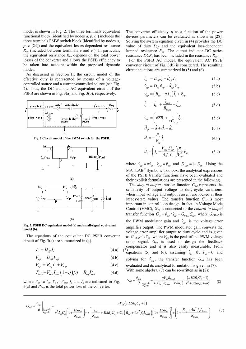
model is shown in Fig. 2. The three terminals equivalent
functional block (identified by nodes a, p, c’) includes the
three terminals PMW switch block (identified by nodes a,
p, c [24]) and the equivalent losses-dependent resistance
Req (included between terminals c and c’). In particular,
the equivalent resistance Req depends on the total power
losses of the converter and allows the PSFB efficiency to
be taken into account within the proposed dynamic
model.
As discussed in Section II, the circuit model of the
effective duty is represented by means of a voltage-
controlled source and a current-controlled source (see Fig.
2). Thus, the DC and the AC equivalent circuit of the
PSFB are shown in Fig. 3(a) and Fig. 3(b), respectively.
Fig. 2.Circuit model of the PWM switch for the PSFB.
(a)
(b)
Fig. 3. PSFB DC equivalent model (a) and small-signal equivalent
model (b).
The equations of the equivalent DC PSFB converter
circuit of Fig. 3(a) are summarized in (4).
a eff cI D I (4.a) (3)
cp eff apV D V (4.b)
cp eq c c pV R I V (4.c)
2= 1loss out out eq outP V I R I (4.d)
where Vap=nVin, Vc’p=Vout, Ic and Ia are indicated in Fig.
3(a) and Ploss is the total power loss of the converter.
The converter efficiency as a function of the power
devices parameters can be evaluated as shown in [28].
Solving the system equation given in (4) provides the DC
value of duty Deff and the equivalent loss-dependent
lumped resistance Req. The output inductor DC series
resistance DCRo has been included in the resistance Req.
For the PSFB AC model, the equivalent AC PSFB
converter circuit of Fig. 3(b) is considered. The resulting
circuit equations are summarized in (5) and (6).
ˆˆ ˆa eff c eff ci D i d I (5.a)
ˆˆ ˆcp eff ap eff apv D v d V (5.b)
ˆˆ ˆcp eq o c c pv R s L i v (5.c)
ˆˆ ˆ ˆoutc Co out
load
vi i i
R (5.d)
1 ˆˆout o Co
o
v ESR isC
(5.e)
ˆ ˆ ˆ ˆeff i vd d d d (6.a)
ˆ ˆdi c
ap
Rd i
V (6.b)
2ˆ ˆ
4
out eff dv c ap
s o ap
V D Rd I v
f L V
(6.c)
where ˆ ˆap inv nv ,
'ˆ ˆ
c p outv v and ' 1eff effD D . Using the
MATLAB® Symbolic Toolbox, the analytical expressions
of the PSFB transfer functions have been evaluated and
their explicit formulations are presented in the following.
The duty-to-output transfer function Gvd represents the
sensitivity of output voltage to duty-cycle variations,
when input voltage and output current are locked at their
steady-state values. The transfer function Gvd is most
important in control loop design. In fact, in Voltage Mode
Control (VMC), Gvd is connected to the control-to-output
transfer function ˆ ˆ/vc out ctr PWM vdG v v G G , where GPWM is
the PWM modulator gain and ˆctrv is the voltage error
amplifier output. The PWM modulator gain converts the
voltage error amplifier output to duty cycle and is given
as GPWM=1/Vpp, where Vpp is the peak of the PWM voltage
ramp signal. Gvc is used to design the feedback
compensator and it is also easily measurable. From
equations (5) and (6), assuming ˆ 0inv , ˆ 0outi and
solving for ˆoutv , the transfer function Gvd has been
evaluated and its analytical formulation is given in (7).
With some algebra, (7) can be re-written as in (8):
2 2ˆ 0
ˆ 0
1ˆ
ˆ 2
o oout in loadvd
iout o o load o n nvin
s ESR Cv nV RG
L C R ESR s sd
(8)
2ˆ 0
2 2ˆ 0
1ˆ
ˆ 41 4 1 1
in o ooutvd
iout eq s leako o ovin o o o o o eq s leakload load load load
nV s ESR CvG
d R n f LESR L ESRs L C s ESR C C R n f L
R R R R
(7)

The natural frequency n and the damping ratio have
the analytical expressions given in (9):
2 2
2
4
2 4
o oload o load eq s leak load
o o
load o load eq s leak
L CR ESR R R n f L R
C L
R ESR R R n f L
(9.a)
241 load eq s leak
n
load oo o
R R n f L
R ESRL C
(9.b)
According to (8), the transfer function Gvd exhibits a
second-order dynamic with a pair of poles, an additional
extra-zero which depends upon the output capacitor, and
a gain related to the output filter parameters, the converter
input and output voltage and the transformer turns ratio.
From equation (9.a) and (9.b), it can be seen how the ESR
of the output capacitor not only adds a zero to PSFB
dynamic system but also impacts the damping ratio , as
well as the natural frequency n. Furthermore, the
appearance of the equivalent resistance Req in the natural
frequency term n also confirms that the resonance will
change according to the PSFB losses. Therefore, the
parasitics cannot simply be neglected. The damping and
resonance properties of the PSFB second-order system
depend on the circuit parasitics, which must be all
properly considered for a correct analysis of the system
transient response. To this end, additional comments can
be found in the paper Appendix.
The line-to-output transfer function Gvg represents the
sensitivity of output voltage to input voltage variations,
when duty-cycle and output current are locked at their
steady-state values. From equations (5) and (6), now
assuming ˆ 0d , ˆ 0outi and solving for ˆoutv , the transfer
function Gvg has been evaluated and its analytical
formulation is given in (10). From network theory it is
known that the polynomial denominator is the same for
all the transfer functions of a dynamic system, as it
depends on the characteristics of the network itself. In
particular, the transfer function Gvg is identical to the
transfer function Gvd, except for the DC gain. The DC
gain of the transfer function Gvg depends on the
voltage/current operating conditions and on the circuit
parasitics, whose effect on the PSFB damping and
resonance properties has already been emphasized for the
Gvd.
Finally, the load-to-output (or output impedance) transfer
function Zout represents the sensitivity of output voltage to
output current variations, when duty-cycle and input
voltage are locked at their steady-state values. From
equations (5) and (6), now assuming ˆ 0d , ˆ 0inv and
solving for ˆoutv , the transfer function Zout has been
evaluated and its analytical formulation is given in (11).
According to (11), the transfer function Zout has a pair of
poles and two extra-zeros, one depending on the ESR of
the output capacitor and another depending on the output
inductor, the equivalent resistance Req, the switching
frequency and the transformer parameters. Also, the
transfer function gain depends on the output filter
parameters and the converter output specifications.
B. Experimental verification
Experimental measurements of the open loop transfer
functions have been realized by means of the Texas
Instruments high-efficiency evaluation board shown in
Fig.4, including the PSFB voltage-mode controller
UCC28950PW[40]. The following operating conditions
were applied: Vin=36V, Vout=14V, Iout=10A, fs=188kHz.
Main power devices mounted on the board are listed in
Table I. All the converter open-loop transfer functions
were measured using the OMICRON Lab Bode 100
vector network analyzer. Numerous small-signal
measurements were performed using analog small-signal
injection techniques [41]. In order to verify the validity of
the proposed dynamic model, measurements of the output
filter components and of the transformer were also carried
out and the following measured values were obtained:
Co=1354uF, ESRo=21.2mΩ, Lo=5.3uH, DCRo=35.4mΩ,
Lleak=191nH. Also, the converter’s efficiency was at
=96.6%.
Fig. 4.PSFB board used for the experimental measurements.
Table I. Main power devices mounted on the board.
Main Devices Part numbers Manufact. Main attributes
Primary
MOSFETs BSC123N08NS3-G Infineon
Vds=80V, Id=55A
Rds,on=12.3mΩ,
Secondary
Diodes ES1D Diodes
Super Fast Rect.,
Vf=0.92V, If=1A
Output
Inductor SER2918H-472 Coilcraft
SMT, L=4.7uH,
DCR=2.86mΩ
Output
Capacitor EEUFK1V152L Panasonic
Aluminum, 35V,
C=1500uF
Input
Capacitor ECA2AHG101 Panasonic
Aluminum, 100V,
C=100uF
Input
Capacitor
C1210C225K1RACTU
(x3) Kemet
Ceramic, 100V,
C=2.2uF
Transformer PN-54922 (Custom) Payton np=4, ns=2,
Pmax=294W
2
2 2ˆ 0ˆ 0
1ˆ 4
ˆ 2
eff o oout o s loadvg eff leak
ioutin in load o o o load o n nd
D s ESR Cv V f RG nD n L
v V R L L C R ESR s s
(10)
2
2 2ˆ 0ˆ 0
4 1ˆ
ˆ 2
eq s leak o o oout loadout
d o o load oout n nvin
R n f L sL s ESR Cv RZ
L C R ESRi s s
(11)

The measured and the simulated results for the control-
to-output transfer function Gvc is shown in Fig. 5: there is
excellent agreement between the experimental result
(dashed gray line) and the proposed PSFB enhanced
dynamic model (black continuous line). Also, the
experimental measurements (dashed gray line) and the
simulated results (black continuous line) for the input-to-
output transfer function Gvg and the load-to-output
transfer function Zout are shown in Fig. 6 and Fig. 7,
respectively. The resulting agreement between the
measured and simulated transfer functions permits to
validate the proposed enhanced model for small-signal
analysis of the PSFB converter.
C. Impact of ESL in the PSFB dynamic model
At higher frequencies the agreement between the
experimental results and the proposed PSFB enhanced
dynamic model can be improved further by taking into
account the effect of the Equivalent Series Inductance of
the output capacitor (labeled in the following as ESLo).
Fig. 5. Measured (dotted lines) and simulated (solid lines) control-
to-output transfer function.
Fig. 6. Measured (dotted lines) and simulated (solid lines) input-to-
output transfer function.
Fig. 7. Measured (dotted lines) and simulated (solid lines) load-to-
output transfer function.
To include the ESLo in the PSFB AC model equation
(5.e) should be replaced by equation (12):
1 ˆˆout o o Co
o
v ESR s ESL isC
(12)
Using a value of ESLo=5nH, experimental and the
simulated results are almost identical to higher frequency
to 1MHz, as shown in Fig. 8. The achieved agreement
once again confirms the accuracy of the proposed
dynamic model.
Nevertheless, it should be noted that typically
frequencies above the open-loop crossover frequency are
of little interest in control loop design. Therefore, the
model without the addition of the ESLo is acceptable for
most use cases.
Fig. 8. Measured (dotted lines) and simulated (solid lines) control-
to-output transfer function including ESLo.
102
103
104
105
-30
-20
-10
0
10
20
30
Frequency [Hz]
Ma
gn
itu
de [
dB
]
102
103
104
105
-150
-100
-50
0
Frequency [Hz]
Ph
ase
[D
eg
rees]
Gvc
- Enhanced Model
Gvc
- Measurement
Gvc
- Enhanced Model
Gvc
- Measurement
102
103
104
105
-60
-40
-20
0
Frequency [Hz]
Ma
gn
itu
de [
dB
]
102
103
104
105
-150
-100
-50
0
Frequency [Hz]
Ph
ase
[D
eg
rees]
Gvg
- Enhanced Model
Gvg
- Measurement
Gvg
- Enhanced Model
Gvg
- Measurement
102
103
104
105
-50
-40
-30
-20
-10
Frequency [Hz]
Ma
gn
itu
de [
dB
]
102
103
104
105
-60
-40
-20
0
20
40
Frequency [Hz]
Ph
ase
[D
eg
rees]
Zout
- Enhanced Model
Zout
- Measurement
Zout
- Enhanced Model
Zout
- Measurement
102
103
104
105
-30
-20
-10
0
10
20
30
Frequency [Hz]
Magn
itu
de [
dB
]
102
103
104
105
-150
-100
-50
0
Frequency [Hz]
Ph
ase
[D
egrees]
Gvc
- Enhanced Model
Gvc
- Measurement
Gvc
- Enhanced Model
Gvc
- Measurement

IV. IMPACT OF THE DYNAMIC MODEL ON PSFB
COMPENSATOR DESIGN
The proposed dynamic model permits reliable
compensator design for the PSFB, with a predictable and
accurate value of the crossover frequency and an
acceptable amount of phase margin. The loop gain of the
converter is given by Tc=Gva Gvc, where Gva is the
compensator gain to be designed based on the control-to-
output transfer function Gvc. Given the design
specifications mentioned in Section III, the Gvc transfer
function can be calculated as derived in the same Section.
In order to clearly understand the impact of an improper
dynamic modeling on the closed loop transfer functions
of the PSFB, the compensator design for the
aforementioned case study is discussed in the remainder
of this section. The compensator has been derived based
on the K-factor approach [42] by using the two following
PSFB dynamic models:
i. the model proposed in this paper, labeled as the
enhanced model, including the parasitic parameters;
ii. the model proposed in [26], labeled as the simplified
model, where 24 0.25s leak loadn f L R and =100%.
The following dynamic specifications have been adopted
for the compensator design: a cross-over frequency
fc=3.5kHz and a phase margin Pm=65°. It should be noted
that a cross-over frequency of around 3kHz - 5kHz is
usually the highest achievable cross-over frequency for an
isolated converter using opto-isolator in the control loop.
Therefore, it is necessary to ensure a predictable value of
fc using the model to comply with this specification. The
compensator design results obtained with the enhanced
and simplified models are shown in Table II.
Table II. Compensator design for enhanced and simplified models.
Model Controller Type Compensator
design
Enhanced
model
2
1 1
, 2
2
2 1 2
1 2
p z
va E
p
f s fG
s s f
fp1=347Hz fz1=1.80kHz
fp2=6.82kHz
Simplified
model
2
1 1
, 2
2
2 1 2
1 2
p z
va S
p
f s fG
s s f
fp1=830 Hz fz1=1.66 kHz
fp2=7.39 kHz
The fulfillment of all the dynamic specifications requires
a Type-III controller, labeled as Gva,E for the enhanced
model and Gva,S for the simplified model. In Fig.9(a) the
uncompensated loop gain Tu,E (gray solid line) and the
compensated loop gain Tc,E=Tu,E Gva,E (black solid line) are
shown for the enhanced model. In Fig.9(b) the
uncompensated loop gain Tu,S (gray solid line) and the
compensated loop gain Tc,S=Tu,S Gva,S (black solid line) are
shown for the simplified model. The switching frequency
fs (dotted gray lines) and the resulting cross-over
frequency fc,E, fc,S (dashed lines) are also shown for the
two models in Fig. 9(a)(b). As can be seen from Fig. 9(a),
the compensator designed using the enhanced model
perfectly fits the dynamic specifications, with a crossover
frequency of 3.5kHz. The compensated loop gain Tc,E-
S=Tu,E Gva,S (dotted black lines) shown in Fig. 9(b) can be
analyzed to understand what happens if the compensator
designed with the simplified model Gva,S is used to control
the real converter with losses. In particular, the plot of
Tc,E-S shows that the cross-over frequency and phase
margin obtained do not comply with the given dynamic
specifications: the resulting cross-over frequency is fc,E-
S=7.8kHz, whereas the cross-over specification is 3.5kHz.
Of course, due to the presence of the opto-coupler pole, a
crossover frequency of twice the designed value, in all
likeliness, would result in instability in a real system. The
additional pole added by the opto-coupler and the higher
than expected crossover frequency could result in the
slope of the compensated loop gain magnitude to
approach 40dB/decade and thus violate the power supply
stability criteria. Moreover, as shown in Fig. 9(b), the
resulting phase margin is 50° whereas the desired phase
margin is 65°. This could lead to stability issues for
systems where additional phase lag can occur, and of
course to lower than permitted Mean Time Between
Failures (MTBF) from a commercial product point.
The analysis of the line step-response of the converter
helps in the better understanding of the impact of power
losses on the reliability of the PSFB compensator design.
The compensated line-to-output transfer function GvgC can
be used for this purpose.
(a)
(b)
Fig. 9. Uncompensated and compensated loop gain transfer
functions for enhanced (a) and simplified (b) model.
100
102
104
106
-160
-80
0
80
160
Frequency [Hz]
Ma
gn
itu
de [
dB
]
Tu, E
Tc, E
fc, E
fs
100
102
104
106
-270
-180
-90
0
90
Frequency [Hz]
Ph
ase
[d
eg
]
100
102
104
106
-160
-80
0
80
160
Frequency [Hz]
Ma
gn
itu
de [
dB
]
Tu, S
Tc, S
Tc, S - real
fc, S
fc, S - real
fs
100
102
104
106
-270
-180
-90
0
90
Frequency [Hz]
Ph
ase
[d
eg
]
Cross-over
@ 3.5kHz
Phase margin
of 65°
Cross-over
@ 7.8kHz
Cross-over
@ 3.5kHz
Phase margin
of 50°
Phase margin
of 65°
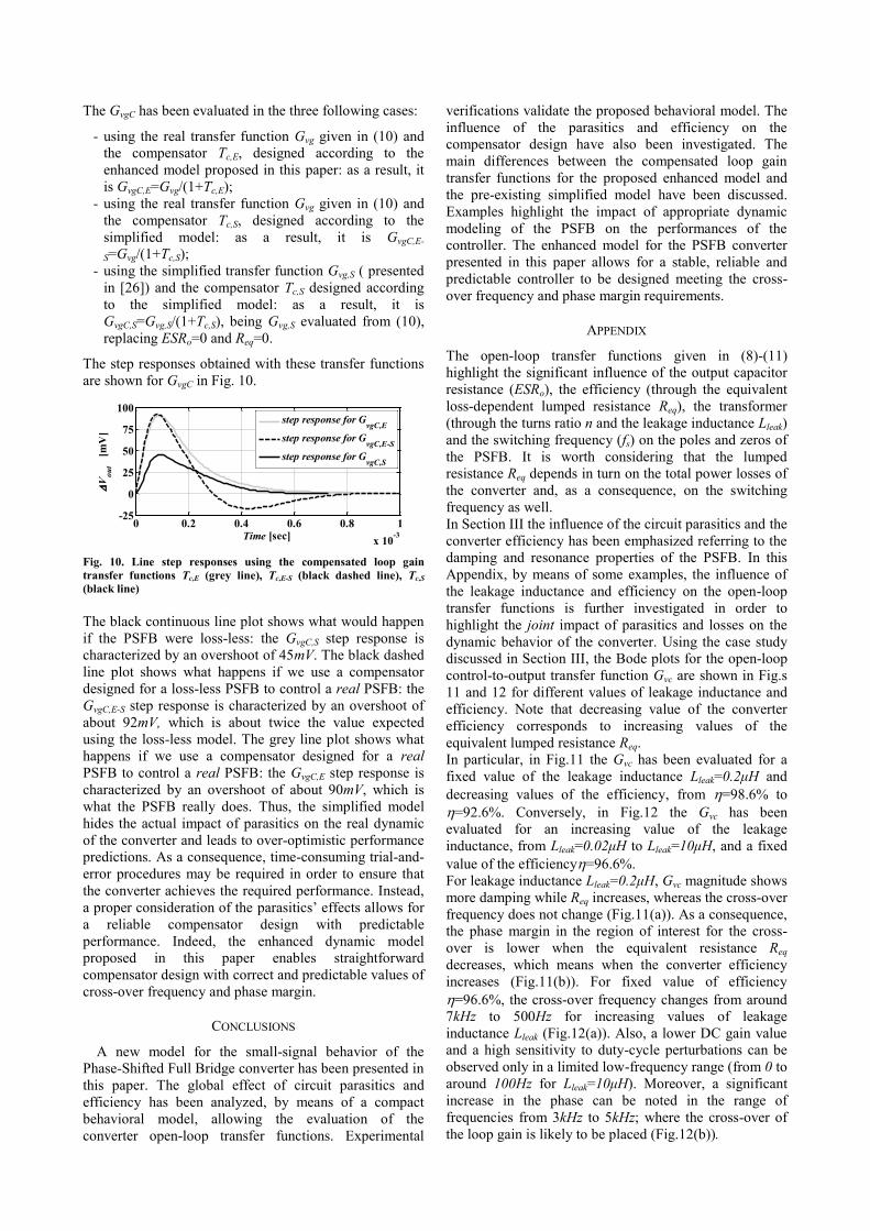
The GvgC has been evaluated in the three following cases:
- using the real transfer function Gvg given in (10) and
the compensator Tc,E, designed according to the
enhanced model proposed in this paper: as a result, it
is GvgC,E=Gvg/(1+Tc,E);
- using the real transfer function Gvg given in (10) and
the compensator Tc,S, designed according to the
simplified model: as a result, it is GvgC,E-
S=Gvg/(1+Tc,S);
- using the simplified transfer function Gvg,S ( presented
in [26]) and the compensator Tc,S designed according
to the simplified model: as a result, it is
GvgC,S=Gvg,S/(1+Tc,S), being Gvg,S evaluated from (10),
replacing ESRo=0 and Req=0.
The step responses obtained with these transfer functions
are shown for GvgC in Fig. 10.
Fig. 10. Line step responses using the compensated loop gain
transfer functions Tc,E (grey line), Tc,E-S (black dashed line), Tc,S
(black line)
The black continuous line plot shows what would happen
if the PSFB were loss-less: the GvgC,S step response is
characterized by an overshoot of 45mV. The black dashed
line plot shows what happens if we use a compensator
designed for a loss-less PSFB to control a real PSFB: the
GvgC,E-S step response is characterized by an overshoot of
about 92mV, which is about twice the value expected
using the loss-less model. The grey line plot shows what
happens if we use a compensator designed for a real
PSFB to control a real PSFB: the GvgC,E step response is
characterized by an overshoot of about 90mV, which is
what the PSFB really does. Thus, the simplified model
hides the actual impact of parasitics on the real dynamic
of the converter and leads to over-optimistic performance
predictions. As a consequence, time-consuming trial-and-
error procedures may be required in order to ensure that
the converter achieves the required performance. Instead,
a proper consideration of the parasitics’ effects allows for
a reliable compensator design with predictable
performance. Indeed, the enhanced dynamic model
proposed in this paper enables straightforward
compensator design with correct and predictable values of
cross-over frequency and phase margin.
CONCLUSIONS
A new model for the small-signal behavior of the
Phase-Shifted Full Bridge converter has been presented in
this paper. The global effect of circuit parasitics and
efficiency has been analyzed, by means of a compact
behavioral model, allowing the evaluation of the
converter open-loop transfer functions. Experimental
verifications validate the proposed behavioral model. The
influence of the parasitics and efficiency on the
compensator design have also been investigated. The
main differences between the compensated loop gain
transfer functions for the proposed enhanced model and
the pre-existing simplified model have been discussed.
Examples highlight the impact of appropriate dynamic
modeling of the PSFB on the performances of the
controller. The enhanced model for the PSFB converter
presented in this paper allows for a stable, reliable and
predictable controller to be designed meeting the cross-
over frequency and phase margin requirements.
APPENDIX
The open-loop transfer functions given in (8)-(11)
highlight the significant influence of the output capacitor
resistance (ESRo), the efficiency (through the equivalent
loss-dependent lumped resistance Req), the transformer
(through the turns ratio n and the leakage inductance Lleak)
and the switching frequency (fs) on the poles and zeros of
the PSFB. It is worth considering that the lumped
resistance Req depends in turn on the total power losses of
the converter and, as a consequence, on the switching
frequency as well.
In Section III the influence of the circuit parasitics and the
converter efficiency has been emphasized referring to the
damping and resonance properties of the PSFB. In this
Appendix, by means of some examples, the influence of
the leakage inductance and efficiency on the open-loop
transfer functions is further investigated in order to
highlight the joint impact of parasitics and losses on the
dynamic behavior of the converter. Using the case study
discussed in Section III, the Bode plots for the open-loop
control-to-output transfer function Gvc are shown in Fig.s
11 and 12 for different values of leakage inductance and
efficiency. Note that decreasing value of the converter
efficiency corresponds to increasing values of the
equivalent lumped resistance Req.
In particular, in Fig.11 the Gvc has been evaluated for a
fixed value of the leakage inductance Lleak=0.2μH and
decreasing values of the efficiency, from =98.6% to
=92.6%. Conversely, in Fig.12 the Gvc has been
evaluated for an increasing value of the leakage
inductance, from Lleak=0.02μH to Lleak=10μH, and a fixed
value of the efficiency=96.6%.
For leakage inductance Lleak=0.2μH, Gvc magnitude shows
more damping while Req increases, whereas the cross-over
frequency does not change (Fig.11(a)). As a consequence,
the phase margin in the region of interest for the cross-
over is lower when the equivalent resistance Req
decreases, which means when the converter efficiency
increases (Fig.11(b)). For fixed value of efficiency
=96.6%, the cross-over frequency changes from around
7kHz to 500Hz for increasing values of leakage
inductance Lleak (Fig.12(a)). Also, a lower DC gain value
and a high sensitivity to duty-cycle perturbations can be
observed only in a limited low-frequency range (from 0 to
around 100Hz for Lleak=10μH). Moreover, a significant
increase in the phase can be noted in the range of
frequencies from 3kHz to 5kHz; where the cross-over of
the loop gain is likely to be placed (Fig.12(b)).
0 2 4 6 8
x 10-4
0
50
100
Time [sec]
V
ou
t [
mV
]
1(t)*Gvg,c - enhan.
1(t)*Gvg,c - simpl.
0 0.2 0.4 0.6 0.8 1
x 10-3
-25
0
25
50
75
100
Time [sec]
V
ou
t [
mV
]
step response for GvgC,E
step response for GvgC,E-S
step response for GvgC,S
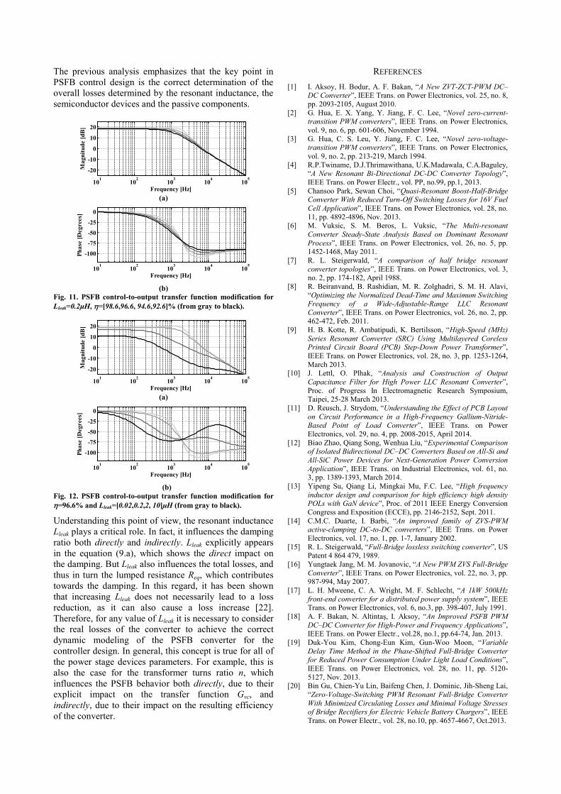
The previous analysis emphasizes that the key point in
PSFB control design is the correct determination of the
overall losses determined by the resonant inductance, the
semiconductor devices and the passive components.
(a)
(b)
Fig. 11. PSFB control-to-output transfer function modification for
Lleak=0.2μH, =[98.6,96.6, 94.6,92.6]% (from gray to black).
(a)
(b)
Fig. 12. PSFB control-to-output transfer function modification for
=96.6% and Lleak=[0.02,0.2,2, 10]μH (from gray to black).
Understanding this point of view, the resonant inductance
Lleak plays a critical role. In fact, it influences the damping
ratio both directly and indirectly. Lleak explicitly appears
in the equation (9.a), which shows the direct impact on
the damping. But Lleak also influences the total losses, and
thus in turn the lumped resistance Req, which contributes
towards the damping. In this regard, it has been shown
that increasing Lleak does not necessarily lead to a loss
reduction, as it can also cause a loss increase [22].
Therefore, for any value of Lleak it is necessary to consider
the real losses of the converter to achieve the correct
dynamic modeling of the PSFB converter for the
controller design. In general, this concept is true for all of
the power stage devices parameters. For example, this is
also the case for the transformer turns ratio n, which
influences the PSFB behavior both directly, due to their
explicit impact on the transfer function Gvc, and
indirectly, due to their impact on the resulting efficiency
of the converter.
REFERENCES
[1] I. Aksoy, H. Bodur, A. F. Bakan, “A New ZVT-ZCT-PWM DC–DC Converter”, IEEE Trans. on Power Electronics, vol. 25, no. 8,
pp. 2093-2105, August 2010.
[2] G. Hua, E. X. Yang, Y. Jiang, F. C. Lee, “Novel zero-current-transition PWM converters”, IEEE Trans. on Power Electronics,
vol. 9, no. 6, pp. 601-606, November 1994.
[3] G. Hua, C. S. Leu, Y. Jiang, F. C. Lee, “Novel zero-voltage-transition PWM converters”, IEEE Trans. on Power Electronics,
vol. 9, no. 2, pp. 213-219, March 1994.
[4] R.P.Twiname, D.J.Thrimawithana, U.K.Madawala, C.A.Baguley, “A New Resonant Bi-Directional DC-DC Converter Topology”,
IEEE Trans. on Power Electr., vol. PP, no.99, pp.1, 2013.
[5] Chansoo Park, Sewan Choi, “Quasi-Resonant Boost-Half-Bridge Converter With Reduced Turn-Off Switching Losses for 16V Fuel
Cell Application”, IEEE Trans. on Power Electronics, vol. 28, no.
11, pp. 4892-4896, Nov. 2013. [6] M. Vuksic, S. M. Beros, L. Vuksic, “The Multi-resonant
Converter Steady-State Analysis Based on Dominant Resonant
Process”, IEEE Trans. on Power Electronics, vol. 26, no. 5, pp. 1452-1468, May 2011.
[7] R. L. Steigerwald, “A comparison of half bridge resonant
converter topologies”, IEEE Trans. on Power Electronics, vol. 3, no. 2, pp. 174-182, April 1988.
[8] R. Beiranvand, B. Rashidian, M. R. Zolghadri, S. M. H. Alavi,
“Optimizing the Normalized Dead-Time and Maximum Switching Frequency of a Wide-Adjustable-Range LLC Resonant
Converter”, IEEE Trans. on Power Electronics, vol. 26, no. 2, pp. 462-472, Feb. 2011.
[9] H. B. Kotte, R. Ambatipudi, K. Bertilsson, “High-Speed (MHz)
Series Resonant Converter (SRC) Using Multilayered Coreless Printed Circuit Board (PCB) Step-Down Power Transformer”,
IEEE Trans. on Power Electronics, vol. 28, no. 3, pp. 1253-1264,
March 2013. [10] J. Lettl, O. Plhak, “Analysis and Construction of Output
Capacitance Filter for High Power LLC Resonant Converter”,
Proc. of Progress In Electromagnetic Research Symposium, Taipei, 25-28 March 2013.
[11] D. Reusch, J. Strydom, “Understanding the Effect of PCB Layout
on Circuit Performance in a High-Frequency Gallium-Nitride-Based Point of Load Converter”, IEEE Trans. on Power
Electronics, vol. 29, no. 4, pp. 2008-2015, April 2014.
[12] Biao Zhao, Qiang Song, Wenhua Liu, “Experimental Comparison of Isolated Bidirectional DC–DC Converters Based on All-Si and
All-SiC Power Devices for Next-Generation Power Conversion
Application”, IEEE Trans. on Industrial Electronics, vol. 61, no. 3, pp. 1389-1393, March 2014.
[13] Yipeng Su, Qiang Li, Mingkai Mu, F.C. Lee, “High frequency
inductor design and comparison for high efficiency high density POLs with GaN device”, Proc. of 2011 IEEE Energy Conversion
Congress and Exposition (ECCE), pp. 2146-2152, Sept. 2011.
[14] C.M.C. Duarte, I. Barbi, “An improved family of ZVS-PWM active-clamping DC-to-DC converters”, IEEE Trans. on Power
Electronics, vol. 17, no. 1, pp. 1-7, January 2002.
[15] R. L. Steigerwald, “Full-Bridge lossless switching converter”, US Patent 4 864 479, 1989.
[16] Yungtaek Jang, M. M. Jovanovic, “A New PWM ZVS Full-Bridge
Converter”, IEEE Trans. on Power Electronics, vol. 22, no. 3, pp. 987-994, May 2007.
[17] L. H. Mweene, C. A. Wright, M. F. Schlecht, “A 1kW 500kHz
front-end converter for a distributed power supply system”, IEEE Trans. on Power Electronics, vol. 6, no.3, pp. 398-407, July 1991.
[18] A. F. Bakan, N. Altintaş, I. Aksoy, “An Improved PSFB PWM
DC–DC Converter for High-Power and Frequency Applications”, IEEE Trans. on Power Electr., vol.28, no.1, pp.64-74, Jan. 2013.
[19] Duk-You Kim, Chong-Eun Kim, Gun-Woo Moon, “Variable
Delay Time Method in the Phase-Shifted Full-Bridge Converter for Reduced Power Consumption Under Light Load Conditions”,
IEEE Trans. on Power Electronics, vol. 28, no. 11, pp. 5120-
5127, Nov. 2013. [20] Bin Gu, Chien-Yu Lin, Baifeng Chen, J. Dominic, Jih-Sheng Lai,
“Zero-Voltage-Switching PWM Resonant Full-Bridge Converter
With Minimized Circulating Losses and Minimal Voltage Stresses of Bridge Rectifiers for Electric Vehicle Battery Chargers”, IEEE
Trans. on Power Electr., vol. 28, no.10, pp. 4657-4667, Oct.2013.
101
102
103
104
105
-20
-10
0
10
20
Frequency [Hz]
Ma
gn
itu
de [
dB
]
Gvc
101
102
103
104
105
-100
-75
-50
-25
0
Frequency [Hz]
Ph
ase
[D
eg
rees]
101
102
103
104
105
-20
-10
0
10
20
Frequency [Hz]
Ma
gn
itu
de [
dB
]
Gvc
101
102
103
104
105
-100
-75
-50
-25
0
Frequency [Hz]
Ph
ase
[D
eg
rees]
101
102
103
104
105
-20
-10
0
10
20
Frequency [Hz]
Ma
gn
itu
de [
dB
]
Gvc
101
102
103
104
105
-100
-75
-50
-25
0
Frequency [Hz]
Ph
ase
[D
eg
rees]
101
102
103
104
105
-20
-10
0
10
20
Frequency [Hz]
Ma
gn
itu
de [
dB
]
Gvc
101
102
103
104
105
-100
-75
-50
-25
0
Frequency [Hz]
Ph
ase
[D
eg
rees]

[21] Xinke Wu, Xiaogao Xie, Junming Zhang, Rongxiang Zhao,
Zhaoming Qian, “Soft Switched Full Bridge DC–DC Converter
With Reduced Circulating Loss and Filter Requirement”, IEEE
Trans. on Power Electr., vol. 22, no. 5, pp. 1949-1955, Sept.2007. [22] M. Hallworth, B. Potter, A. Shirsavar, “Analytical calculation of
resonant inductance for zero voltage switching in phase-shifted
full-bridge converters”, IET Power Electronics, vol. 6, n. 3, pp. 523-534, March 2013.
[23] S. R. Sanders, J. M. Noworolski, X. Z. Liu, G. C. Verghese,
“Generalized averaging method for power conversion circuits”, IEEE Trans. on Power Electr., vol.6, no.2, pp.251-259, Apr.1991.
[24] V. Vorperian, “Simplified analysis of PWM converters using
model of PWM switch. Continuous conduction mode”, IEEE Trans. on Aerospace and Electronic Systems, vol. 26, no. 3, pp.
490-496, May 1990.
[25] J. A. Sabate, V. Vlatkovic, R. B. Ridley, F. Lee, B. H. Cho, “Design considerations for high-voltage high-power full-bridge
zero-voltage-switched PWM converter”, Proc. of the5thAnnual
Applied Power Electronics Conference and Exposition (APEC’90), pp. 275-284, 11-16 March 1990.
[26] V. Vlatkovic, J. A. Sabate, R. B. Ridley, F. C. Lee, B. H. Cho,
“Small-signal analysis of the phase-shifted PWM converter”, IEEE Trans. on Power Electr., vol.7, no.1, pp.128-135, Jan 1992.
[27] M. J. Schutten, D. A. Torrey, “Improved small-signal analysis for
the phase-shifted PWM power converter”, IEEE Trans. on Power Electronics, vol. 18, no. 2, pp. 659-669, March 2003.
[28] Bo-Yuan Chen, Yen-Shin Lai, “Switching Control Technique of
Phase-Shift-Controlled Full-Bridge Converter to Improve Efficiency Under Light-Load and Standby Conditions Without
Additional Auxiliary Components”, IEEE Trans. on Power
Electronics, vol. 25, no. 4, pp. 1001-1012, April 2010. [29] Chen Zhao, Xinke Wu, Peipei Meng, Zhaoming Qian, “Optimum
Design Consideration and Implementation of a Novel
Synchronous Rectified Soft-Switched Phase-Shift Full-Bridge Converter for Low-Output-Voltage High-Output-Current
Applications”, IEEE Trans. on Power Electronics, vol. 24, no. 2,
pp. 388-397, Feb. 2009 [30] Kyu-Min Cho, Young-Do Kim, In-Ho Cho, Gun-Woo Moon,
“Transformer Integrated With Additional Resonant Inductor for
Phase-Shift Full-Bridge Converter With Primary Clamping Diodes”, IEEE Trans. on Power Electronics, vol. 27, no. 5, pp.
2405-2414, May 2012.
[31] Young-Do Kim, Kyu-Min Cho, Duk-You Kim, Gun-Woo Moon, “Wide-Range ZVS Phase-Shift Full-Bridge Converter With
Reduced Conduction Loss Caused by Circulating Current”, IEEE
Trans. on Power Electr., vol. 28, no. 7, pp. 3308-3316, July 2013. [32] S. Shekhawat, M. Rinehimer, B. Brockway, “FCS Fast Body
Diode MOSFET for Phase Shifted ZVS PWM Full Bridge DC-DC
Converter”, Fairchild Semicond., AN-7536, available on line. [33] F. Di Domenico, R. Mente, “ZVS Phase Shift Full Bridge: CFD2
Optimized Design”, Infineon, AN-2013/03, available on line.
[34] Ajay Hari, “Using a Phase-Shifted Full-Bridge Topology in Small Form Factor Power Converters”, National Semiconductor,
SNVA-610, available on line. [35] Jianjiang Shi, Jie Luo, Xiangning He, “Common-Duty-Ratio
Control of Input-Series Output-Parallel Connected Phase-shift
Full-Bridge DC–DC Converter Modules”, IEEE Trans. on Power Electronics, vol. 26, no. 11, pp. 3318-3329, Nov. 2011.
[36] H. Nene, “Digital Control of a Bi-Directional DC-DC Converter
for Automotive Applications”, Proc. of the 28th Annual Applied Power Electronics Conference and Exposition (APEC’13), pp.
1360-1365, 17-21 March 2013.
[37] Gun-Sen Ho, Chiao-Chin Lin, Shin-Hau Hsu, Ying-Yu Tzou, “SoPC based digital current-mode control of full-bridge phase-
shifted DC/DC converters with fast dynamic responses”, IEEE
10th International Conference onPower Electronics and Drive Systems (PEDS), pp. 113-118, 22-25 April 2013.
[38] Jeong-Gyu Lim, Se-Kyo Chung, Yujin Song, “FPGA-based
digital current mode controller for phase-shifted full-bridge PWM converter”, Proc. of IEEE Energy Conversion Congress
and Exposition (ECCE’09), pp. 2840-2846, 20-24 Sept. 2009.
[39] Faa-Jeng Lin, Ming-Shi Huang, Po-Yi Yeh, Han-Chang Tsai, Chi-Hsuan Kuan, “DSP-Based Probabilistic Fuzzy Neural
Network Control for Li-Ion Battery Charger”, IEEE Trans. on
Power Electronics, vol. 27, no. 8, pp. 3782-3794, Aug. 2012. [40] Texas Instruments, “Green Phase-Shifted Full-Bridge Controller
with Synchronous Rectification”, available on-line.
[41] Ridley Engineering, “AP 200 Parallel Frequency Response Analyzer”, Application Notes, available on-line.
[42] H. D. Venable, “The k-factor: A New mathematical Tool for
Stability, Analysis, and Synthesis”, Proc. of PowerCon 10, San Diego, CA, 22-24 March 1983.
Giulia Di Capua Giulia Di Capua (S’06, M’13)
was born in Avellino, Italy, in 1984. She received the B.S. Degree and the M.S. Degree in
Electronic Engineering from the University of
Salerno, with honors, in 2006 and 2009, respectively. She received the PhD degree from
the Doctoral School of Information Engineering
at the same University, in 2013. She is currently a Research Fellow in the Department of
Information Engineering, Electrical Engineering
and Applied Mathematics of the University of Salerno. Her research interests include analysis and design of Power
Management switching mode power supplies, with special attention to
optimization switching converters and of magnetic components for
isolated converters and to thermal characterization of magnetic core for
power components in high-frequency switching applications.
Seyed Ali Shirsavar received the B.Eng.
(Hons.) degree in electronic engineering and the
Ph.D. degree from the University of Reading, Reading, U.K., in 1992 and 1998, respectively.
After a period of work in the industry designing
embedded controller hardware, switch-mode power supplies, and high-performance three-
phase inverters, he is currently a Lecturer in the
University of Reading, where he teaches courses at all levels. His main research interests
include power electronics and in particular digital control of switch
mode power supplies.
Michael Andrew Hallworth (M'11) received
the B.Eng. (Hons.) degree in Electronic
Engineering and the Ph.D degree from the
University of Reading, Reading, U.K., in 2009
and 2013 respectively. He is currently working in the power electronics
industry and is also continuing further research
for the University of Reading. His main research topics include high efficiency
power conversion and the digital control of
switched mode power supplies.
Nicola Femia (M’94, SM’13) was born in
Salerno, Italy, in 1963. He received the Master Degree in Industrial Technologies Engineering
from the Salerno University, with honors, in 1988.
From 1990 to 1998, he was an Assistant
Professor, from 1998 to 2001, he was an Associate Professor, and since 2001, he has
been a Full Professor of Circuits Theory with
the Department of Information and Electrical Engineering, University of Salerno. He is the coauthor of more than 110
scientific papers published in the proceedings of international symposia
and in international journals. His main scientific interests include the fields of circuit theory and applications and power electronics. Dr.
Femia was an Associate Editor for the IEEE Transactions on Power
Electronics from 1995 to 2003.