Energy-Efficient, Noise-Tolerant CMOS Domino VLSI Circuits in ...

An Energy-Efficient CMOS Image Sensor with Embedded
Machine Learning Algorithm
by
Kyuseok Lee
A dissertation submitted in partial fulfillment
of the requirements for the degree of
Doctor of Philosophy
(Electrical Engineering)
in the University of Michigan
2019
Doctoral Committee:
Professor Euisik Yoon, Chair
Associate Professor James W. Cutler
Professor Emeritus Kensall D. Wise
Associate Professor Zhengya Zhang

ii
DEDICATION
To my beloved family for all their support and patience during my years of study

iii
ACKNOWLEDGMENTS
I would first like to thank my research advisor, Prof. Euisik Yoon, for all his support and
advice during my Ph.D. study at University of Michigan, Ann Arbor. This work would not
have been possible without his insightful advice. I would also like to express my
appreciation to my doctoral committee members, Prof. Ken Wise, Zhengya Zhang and
James Cutler, for their participation, invaluable advice, and comments for this research
work.
I would also like to thank my former and current co-workers in Yoon Lab: Seong-Yun ,
Hyunsoo, Seokjun, Sun-il, Jaehyuk, Khaled, Jihyun, Kyounghwan, Xia, Fan, Patrick, Yu-
Chih, Adam, Yu-Ju, Komal, Yu-Heng, Zhixiong and Buke for their helpful suggestions,
discussions, and technical support.
Finally, my deepest gratitude goes to my parents, for all the sacrifices they made to make
my life better. I would also like to express my sincere gratitude to my beloved family,
Jeongeun, Mingi, Dohyeon and Eugene for all their love and understanding and support
throughout the years.

iv
TABLE OF CONTENTS
DEDICATION .................................................................................................................... ii
ACKNOWLEDGMENTS ................................................................................................. iii
LIST OF FIGURES .......................................................................................................... xv
LIST OF TABLES ............................................................................................................ xv
ABSTRACT ................................................................................................................... xviii
Chapter 1 Introduction ........................................................................................................ 1
1.1 Motivation .................................................................................................................. 1
1.2 Embedded-machine learning systems in CMOS image sensor technology ............... 3
1.3 Challenges .................................................................................................................. 4
1.4 Research Goal ............................................................................................................ 6
1.5 Thesis Outline ............................................................................................................ 7
Chapter 2 Introduction of CMOS image sensor ................................................................. 9
2.1 Photodiode ................................................................................................................. 9
2.2 CMOS pixel operation ............................................................................................. 10
2.2.1 Passive pixel sensor ........................................................................................... 11
2.2.2 3-T active pixel sensor ....................................................................................... 12
2.2.3 4-T active pixel sensor ....................................................................................... 14

v
2.3 Pixel performance .................................................................................................... 15
2.3.1 Fill Factor ........................................................................................................... 15
2.3.2 Dark current ....................................................................................................... 16
2.3.3 Full-Well capacity .............................................................................................. 16
2.3.4 Sensitivity .......................................................................................................... 17
2.3.5 Dynamic range ................................................................................................... 18
Chapter 3 Machine-learning algorithm for computer vision ............................................ 19
3.1 Introduction .............................................................................................................. 19
3.2 Application for machine-learning algorithm ........................................................... 20
3.3 Machine-learning operation ..................................................................................... 21
3.3.1 Feature extraction.............................................................................................. 21
3.3.2 Classification..................................................................................................... 22
Chapter 4 CMOS image sensor with embedded objection detection for a vision based
navigation system ............................................................................................. 23
4.1 Introduction .............................................................................................................. 23
4.2 Sensor Architecture .................................................................................................. 27
4.2.1 Pixel architecture ............................................................................................... 31
4.3 HOG based object detection core operation ............................................................ 32
4.3.1 2-b spatial difference image and LUT-based orientation assignment .............. 34
4.3.2 Cell-based SVM classification operation........................................................... 38

vi
4.3.3 Object Searching Scheme .................................................................................. 41
4.4 Implementation and Experimental Result ................................................................ 42
4.4.1 2D optic flow estimation and object detection result from real moving object . 43
4.4.2 Object detection accuracy test ........................................................................... 45
4.4.3 Performance summary and comparison ............................................................. 45
4.5 Summary and chapter conclusion ............................................................................ 47
Chapter 5 CMOS image sensor with embedded mixed-mode convolution neural network
for object recognition ....................................................................................... 49
5.1 Introduction .............................................................................................................. 49
5.2 Circuit architecture................................................................................................... 52
5.3 Circuit implementation ............................................................................................ 53
5.3.1 Mixed-mode MAC architecture ......................................................................... 53
5.3.2 Passive charging sharing based multiplier ......................................................... 55
5.3.3 Energy-efficient algorithm optimization for CNN ............................................ 57
5.4 Evaluation results of proposed CNN ....................................................................... 60
5.5 Implementation and Experimental result ................................................................. 63
5.5.1 Experimental result ............................................................................................ 64
5.5.2 Performance summary and comparison ............................................................. 69
5.6 Summary .................................................................................................................. 70

vii
Chapter 6 Concurrent energy Harvesting and imaging sensor system for distributed IoT
sensor with embedded-learning algorithm ....................................................... 72
6.1 Introduction .............................................................................................................. 72
6.2 Circuit architecture................................................................................................... 73
6.3 Pixel architecture ..................................................................................................... 74
6.4 CMOS imager operation for energy harvesting and imaging modes ...................... 77
6.5 Experiment results ................................................................................................... 78
6.6 Summary and comparison ........................................................................................ 80
Chapter 7 Summary and future work ................................................................................ 83
7.1 Summary .................................................................................................................. 83
7.2 Future work .............................................................................................................. 84
BIBLIOGRAPHY ............................................................................................................. 86

xv
LIST OF FIGURES
Figure 1-1 Architecture of CMOS image sensor with embedded machine-learning algorithm. .... 7
Figure 2-1 Vertical structure of a p-n photodiode ........................................................................ 10
Figure 2-2 Passive pixel readout circuit ........................................................................................ 12
Figure 2-3 3-T active pixel structure ............................................................................................ 14
Figure 2-4 4-T active pixel structure ............................................................................................ 15
Figure 4-1 The Flight time against mass of MAV [36]. ............................................................... 24
Figure 4-2 Operation of vision based navigation system.............................................................. 25
Figure 4-3 Operation of vision based navigation system.............................................................. 29
Figure 4-4 Architecture of proposed vision based navigation image sensor. ............................... 30
Figure 4-5 Reconfigurable pixel architecture ............................................................................... 32
Figure 4-6 Block diagram of object detection core ...................................................................... 33
Figure 4-7 Detection rate precision versus pixel resolution and normalized ADCs power.......... 37
Figure 4-8 SVM classification architecture .................................................................................. 39
Figure 4-9 Cell-based pipeline operation for SMV classifier ....................................................... 40
Figure 4-10 Object search scheme to reduce the false positive .................................................... 41

xvi
Figure 4-11 Chip micrograph........................................................................................................ 42
Figure 4-12 Measured 2D optic flows of moving objects and object detection ........................... 44
Figure 5-1 CNN complexity and ILSVRC top 5 object recognition error rate ............................ 50
Figure 5-2 (a) Conventional CNN system, (b) Proposed low-power CNN real-time imager
with the mixed-mode MACs ..................................................................................... 51
Figure 5-3 CIS architecture with embedded convolution neural network algorithm ................... 53
Figure 5-4 Proposed mixed-mode MAC architecture ................................................................... 54
Figure 5-5 Proposed mixed-signal accumulator operation ........................................................... 55
Figure 5-6 Operation of the passive charge-redistribution multiplier .......................................... 56
Figure 5-7 Proposed hardware and energy efficient CNN operation ........................................... 58
Figure 5-8 2nd layer MAC operation to support proposed CNN scheme ..................................... 59
Figure 5-9 Object recognition simulation result ........................................................................... 63
Figure 5-10 Die microphotograph of CMOS image sensor with embedded mixed-mode
convolution neural network ....................................................................................... 64
Figure 5-11 Relative accuracy of simulation and experimental result as a function of the number
or output quantization bits. ........................................................................................ 65
Figure 5-12 Extracted the intermediate result of CNN layers with proposed relative accuracy of
simulation and experimental result as a function of the number or output quantization
bits. ............................................................................................................................ 67
xvii
Figure 5-13 Chip evaluation result and comparison of the IOU evaluation ................................. 68
Figure 6-1 Energy harvesting image (EHI) sensor architecture ................................................... 74
Figure 6-2 Circuit diagram of the energy harvesting image sensor and the proposed pixel structure
................................................................................................................................... 76
Figure 6-3 Timing diagram of the image readout and energy harvesting circuits ........................ 78
Figure 6-4 Measured harvesting voltage, power, chip power consumption as a function of
illumination levels ..................................................................................................... 79
Figure 6-5 Test images of a U.S. hundred dollar bill at VDD = 0.6V .......................................... 80
Figure 6-6 Energy harvesting CMOS image sensor chip photograph .......................................... 81

xv
LIST OF TABLES
Table 4-1 Spatial difference encoding table ..................................................................... 35
Table 4-2 LUT-based Orientation assignment .................................................................. 36
Table 4-3 Chip characteristics .......................................................................................... 46
Table 4-4 Performance comparison with previous works ................................................ 47
Table 5-1 Performance summary of this works ................................................................ 70
Table 6-1 Performance summary and comparison table ................................................... 82

xviii
ABSTRACT
In this thesis, an energy-efficient CMOS (Complementary Metal–Oxide
Semiconductor) image sensor for embedded machine-learning algorithms has been studied
to provide low-power consumption, minimized hardware resources, and reduced data
bandwidth in both digital and analog domains for power-limited applications. In power-
limited applications, image sensors for embedded machine learning algorithms typically
have these challenges to address: low-power operation from limited energy sources such
as batteries or energy harvesting units, large hardware area due to complicated machine-
learning algorithms, and high-data bandwidth due to video streaming images and large data
movement for evaluating the machine-learning algorithms.
This research focuses on developing the architectures, algorithm optimization, and
associated electronic circuits for an energy-efficient CMOS image sensor with the
embedded machine-learning algorithms. Three interdependent prototypes have been
developed to solve major challenges: minimization of energy consumption and hardware
resources while preserving a high degree of precision in machine-learning algorithm
evaluation. Three prototypes have been fabricated and fully characterized to address these
challenges.
In the first chip, we implemented 2 bit spatial difference imaging, a customized
look-up table (LUT) based gradient orientation assignment, and a cell-based supporting-
vector-machine (SVM) to achieve both low-data bandwidth and higher area efficiency for
xix
a histogram-of-oriented-gradient (HOG)-based object detection. The proposed HOG-based
object detection core operates with the 2D optic flow core to provide the vision-based
navigation functionality for the nano-air-vehicle (NAV) application. The system operates
at 244 pJ/pixel in 2D optic flow extraction mode and at 272.49 pJ/pixel in hybrid operation
mode, respectively. The system achieved 75% reduction in memory size with proposed
HOG feature extraction method and cell-based supporting-vector-machine (SVM).
In the second chip, a mixed-mode approximation arithmetic multiplier-accumulator
(MAC) is built to reduce power consumption for the most power-hungry component in a
convolution neural network image sensor. The proposed energy-efficient convolution
neural networks (CNN) imager operation is as follows. The pixel array gathers photons
and converts them to electrons. The individual pixel values are transferred to a column-
parallel mixed-mode MACs in a rolling shutter fashion. The column-parallel mixed-mode
MACs conduct the convolution operation in the analog-digital mixed-mode signal domain.
Each convolution layer in the neural network is processed in a pipeline fashion. In the last
stage, an analogue-to-digital converter (ADC) converts the result of the MACs operation
to digital signals. Consequently, the column-parallel mixed-mode MACs and the pipeline
operation allow the imaging system to achieve real-time imaging with low-power operation
during runtime. The system operates at 5.2 nJ/pixel in normal image extraction mode and
at 4.46 GOPS/W in a convolution neural network (CNN) operation mode, respectively.
In the third chip, a self-sustainable CMOS image sensor with concurrent energy
harvesting and imaging has been developed to extend the operation time of the machine-
learning imager in the energy-limited environment. The proposed CMOS image sensor
employs a 3T pixel which deploys vertically both hole-accumulation photodiode and

xx
energy harvesting diode in the same pixel to achieve a high fill-factor (FF) and high-energy
harvesting efficiency. The sensor achieved -13.9 pJ/pixel at 30 Klux (normal daylight), 94%
FF for the energy harvesting diode, and 47% FF for the imaging sensing diode.

1
Chapter 1
Introduction
1.1 Motivation
In the past few decades, there has been significant progress in the development of
digital imaging systems with a fast advance in Charge Coupled Device (CCD) and CMOS
Image Sensor (CIS) technologies. CCD was invented by George Smith and Willard Boyle
at Bell Telephone Laboratories (Bell Labs) in the 1970s [1]. This invention transformed
still and video cameras from film to electronic file recording devices. CCD digital imaging
systems rapidly replaced the previous imaging system formats and expanded their area of
influence to digital still cameras, digital camcorders, surveillance cameras, satellite
telescope imaging systems, and more devices. In addition, the industry invented a variety
of new devices such as digital document scanners, bar code readers, digital copiers, and
dozens of other business tools. In the 1990s, the CIS was explored as a competitive digital
imaging for space applications at the National Aeronautics and Space Adminstration’s
(NASA) Jet Propulsion Laboratory. Eric Fossum conducted the research to make CIS “for
space applications in which it has several advantages over CCDs, including a requirement
for less power and less susceptibility to radiation damage in space.” [2]. This earnest
research led to the development of CMOS active-pixel sensors which included additional
functionality, allowing for more portability, achieving lower-power dissipation, and
reducing the imaging systems’ form factor. These key features meant the CMOS image

2
sensor could be integrated with handheld mobile devices such as cellular phones, laptops,
and tablet PCs in the 1990s. Moreover, this evolution was accelerated since CIS
manufacturing used standard CMOS technology, which reduced production cost
significantly. Furthermore, many researchers made progress to improve the key features of
CIS: high spatial resolution [3], high dynamic range [4], high sensitivity [5], low noise [6],
and high-speed imaging [3]. Due to these benefits, CIS replaced CCDs in most digital
imaging systems [7].
Currently, the imaging systems require a paradigm shift due to the emergence of
distributed sensor networks and Internet-of-Things (IoT). IoT devices need the sensors
which can keep monitoring environments and support a User Interface (UI). Due to this
demand, imaging systems are expected to not only acquire simple images or video
streaming images but also to infer images by analyzing scenes from a collected vision
information. Recently, machine learning has made great progress in the accuracy of object
detection tasks and object classification tasks for the imaging processing area. Furthermore,
deep-learning techniques show great improvement in accuracy of inferring images and
image classification areas due to the innovation and application of deep-learning
algorithms [8]. Furthermore, in image classification tasks, deep-learning has surpassed
human accuracy [9-10].
In the rest of this chapter, opportunities for the application of embedded machine
learning algorithms are elaborated with background knowledge of CMOS image sensor
technology. After describing the challenges, we then present our research goals.
3
1.2 Embedded-machine learning systems in CMOS image sensor technology
Even though the CMOS image sensor was invented before CCD technology, CMOS
has not been more widely used than CCD image sensors due to the low signal-to-noise
ratio (SNR) of CMOS image sensors compared to CCD image sensors. In the 1990s, the
CMOS image sensors were rapidly expanding areas of application due to the low power
consumption, low-cost, integration ability, and scalability [1]. The CMOS image sensor
provides a single-chip solution since the CMOS imager, the analog-digital-converters
(ADC), periphery circuits, and digital image processing circuit are implemented together
with standard CMOS technology without additional silicon fabrication processes. However,
the CCD imaging system requires a special silicon fabrication process and off-chip
components (ADCs, the digital imaging processor, and CCD imager controller): as a result,
the fabrication cost of digital imaging systems dependent upon CCD technology is higher
than the fabrication cost of a single-chip solution with CMOS image sensor technology.
Most recently-manufactured CMOS image sensors employ an active pixel sensor (APS)
architecture. Compared to a passive pixel sensor (PPS) architecture, APS shows higher
SNR due to less leakage current which is induced by a selection transistor at each passive
pixel. The APSs deploy an in-pixel amplifier to overcome this problem. In addition, the in-
pixel amplifier allows an increase of higher spatial resolution, which can be helpful to
overcome large parasitic capacitance of column lines in high spatial resolution CMOS
image sensors.
Traditionally, the machine-learning algorithms require large computation resources
and movement of large data files. This means the hardware for implementing machine-
learning algorithms requires memory to store and read the weight values for evaluation and

4
partial calculation results from process elements (PE). CMOS image sensor manufacturing
uses standard CMOS technology: this key feature of the CMOS image sensor allows
implementation of static random access memory (SRAM), an efficient memory unit, and a
high-speed arithmetic logic unit (ALU) which are successfully employed in state-of-art
microprocessor technology in a single-chip solution. However, the machine-learning
algorithm has to process a massive amount of data under a strict time. These constraints
lead to high power consumption and large hardware areas in service of the high-speed
imaging processing unit. To solve these problems, in-pixel imaging processing techniques
are suggested for the imaging process and the embedded machine-learning applications,
which are developed for optimal partitioning between an in-pixel analog process unit (APU)
and a digital signal processor (DPS) [11-13]. In addition, by adapting an angle sensitive
filter in front of pixels with the metal grid, researchers have tried to solve the
aforementioned problems [14].
1.3 Challenges
Recently, machine-learning algorithms are employed at the chip level, giving more
accurate, faster and more energy-efficient computational tasks. Several papers report
reducing power consumption for CMOS image sensors [12-14] [18] [21]. Previous works
show meaningful achievements by adapting several techniques: voltage scaling, in-pixel
ADCs, small-sized pixel architecture, etc. However, CMOS technology scaling has started
to slow down. In addition, to achieve higher performance, the complexity of state-of-the-
art machine-learning algorithms is dramatically increasing [15]. Furthermore, the system
power budget for power-limited applications such as battery capacity has not improved,

5
roughly, at the same rate. These constraints are why low-power operation for embedded
machine-learning operation is needed.
Most of today’s machine-learning algorithms are designed to achieve higher
accuracy of object recognition. Typical examples for floating-point based algorithms are;
neural networks (NN), support vector machines (SVM) [16], principal component analysis
(PCA), the Kanade Lucas Tomasi point tracking algorithm (KLT), and histogram of
oriented gradients (HOG). Floating-point operations require a complicated circuit and a
large area compared to a fixed-point operation approach. In addition, a floating-point
operation is at least 10 times slower than pure integer arithmetic. This speed penalty
demands more system resources to achieve system requirements. Furthermore,
aforementioned machine-learning algorithms use vector/matrix operations and multiplying
to evaluate algorithms. These complicated operations lead towards necessity of a larger
hardware resource relative to classical algorithm approach
A moderate image spatial resolution of 1 megapixel at 30fps results in a bandwidth
requirement of over 0.5 Gbps. In addition, recent machine-learning algorithms require
large data movement to store or load the weight vector information and intermediated
calculation results. For example, to implement AlexNet, the neural network processor
requires 2.8Gb data transmission between PEs and memory (Registers File, SRAM, or
DRAM). In addition, the complexity of the machine-learning algorithms increase the
number of the weight value, which introduces higher data bandwidth demands.

6
1.4 Research Goal
The main goal of this work is implementing an energy-efficient CMOS image sensor
system with an embedded machine-learning algorithm. Traditionally, the imaging systems
used separate image sensors and digital processors/controllers; this approach results in a
large form factor and resultant power consumption due to the power demanded by
communication between each component. This approach is not suitable for power-limited
distributed image sensor networks and IoT applications. Recently, the integration of the
image sensing arrays and processing units together on chip has shown promising results
[11-13]. Figure 1-1 describes the CMOS imaging system architecture with an embedded
machine-learning algorithm consisting of essential circuit blocks for a complete system.
The imaging sensing array is crucial to converting light signals into electrical signals. In
addition, design optimization for this image sensing array block should be made. The
design of the embedded machine-learning block should also be carefully planned and
constructed since it consumes most of the total energy and occupies most of the system
area. In addition, the energy-harvesting block and power management block are required
to extend the lifetime of the system. In this thesis, we achieve the main goals of the
minimization of energy demand, lowered consumption of data bandwidth and efficient
allocation of hardware resources by optimizing the machine-learning algorithm and
architecture in both the digital domain and analog domain. In addition, a photovoltaic
energy harvesting pixel is implemented for energy sources for the proposed system without
additional area penalty of photodiodes and the degradation of energy-harvesting
efficiency. Those three inter-related projects are the main topic of this thesis.

7
Figure 1-1 Architecture of CMOS image sensor with embedded machine-learning
algorithm.
1.5 Thesis Outline
Chapter 2 covers the basic operation of the CMOS image sensor including
architecture and components to support the CMOS image sensor. Furthermore, an in-pixel
photovoltaic energy harvesting method will be introduced for the CMOS image sensor.
Chapter 3 covers background research of the machine-learning algorithm. Chapter 4 covers
the architecture and circuit implementation of a histogram-of-oriented-gradient (HOG)
based object detection to achieve both low data bandwidth and area efficiency in the digital
domain for Nano Air vehicles (NAV). Then, measurement analysis results from the
fabricated chip, and comparison with the other state-of-the-art object detection works will
be shown. Chapter 5 introduces the mixed-mode approximated arithmetic MAC to reduce
the power consumption for the most power-hungry component in the convolution neural

8
network algorithm. In chapter 6, a CMOS image sensor with concurrent energy harvesting
and imaging is discussed to extend the operation time of the machine-learning imager in
an energy-limited environment. This last chapter summarizes this thesis by pointing out
important results and suggests possible future work.

9
Chapter 2
Introduction of CMOS image sensor
CMOS image sensor measure the number of incident photons with the photodiode.
The CMOS image sensor provide the digital image signal from the measured number of
incident photons. The photodiode in each pixel converts the incident light into an electrical
signal. The electrical signal is done through correlated-double sampling (CDS) for noise
cancelation and amplification for suppressing the input-referred noise. This noise-
suppressed analog signal is converted into the digital signal by the embedded ADCs. This
converted digital image is then stored in a digital memory and transmitted outside of the
sensor chip through the interfacing circuits.
In this chapter, the CMOS image sensor background knowledge is presented. First,
the device structure of photodiodes and various pixel structure are introduced. We also
present the ADCs architecture for CMOS image sensor.
2.1 Photodiode
A p-n junction photodiode is common optical sensing device in most CMOS image
sensor. Figure 2-1 depicts the vertical structure of a p-n photodiode. The most p-n
photodiode is formed with n+/pwell or with nwell/p-sub in standard CMOS process. The
p-n photodiode is usually operating in reversed-biased with grounded anode and floated
cathode. The reverse bias is expanding a depletion region and an electric field around the

10
junction, which increase the chance for generating an electron-hole pair. When an incident
photon is arriving the depletion region and the photon energy is higher than the bandgap
energy of silicon, the electron-hole pair is generated. This generated electron-hole pair
within the depletion region are separated by the electric field. Separated holes are drained
by the ground and electrons are collected in the floating cathode. As the result, large
photodiodes depletion region can increase the higher photocurrent. This lager depletion
region can be achieved by adopting lower doping concentration for p-n junction and higher
reverse bias.
Figure 2-1 Vertical structure of a p-n photodiode
2.2 CMOS pixel operation
The photocurrent which generated by incident photon is integrated in the junction
capacitance of PD as shown in Figure 2-1. The CMOS pixel operations are as follows: (1)
A reset transistor (RST) set the PD cathode (VR) to make reverse bias condition for PD
before starting the photocurrent integration in the junction capacitance of PD (2) After the

11
reset operation, the generated electron by the incident photon are collated in the potential
well. This photocurrent discharge the junction capacitance during the integration time. (3)
After TINT, the difference between the VR voltage and the discharged voltage of the PD is
read out, which represent the light intensity. (4) Reset again for next frame.
The accumulated charge in the capacitor or the voltage difference across the diode by
photocurrent can be read out by typically two ways: passive pixel sensor (PPS) and active
pixel sensor (APS). In the following sections, each pixel architecture will be elaborated
and discuss their advantages and disadvantages.
2.2.1 Passive pixel sensor
Figure 2-2 shows a passive pixel sensor structure. In the PPS structure, charges, which
are accumulated in photodiode junction capacitor, are transferred to amplifier for
measuring the total number of generated charges by incident light. In the PPS, pixel include
a switch transistor between the photodiode and the column line, which is used for reset
operation and multiplexing the photodiodes to the amplifier.
The operation of PPS are as follows: (1) First, the photodiode is reset as the virtual ground
voltage of the column amplifier (VREF). (2) The photodiode integrate the charge during
integration time. (3) After the integration time, the collected charges are transferred to the
feedback capacitor CF of the amplifier and the output voltage (VOUT) is amplified. The
VOUT is expressed as:
𝑉𝑂𝑈𝑇 =∆𝑄
𝐶𝐹=𝐶𝑃𝐷𝐶𝐹
∆𝑉

12
, where ΔQ is the generated charges and ΔV is the voltage difference due to the discharge
of the photocurrent. The most attractive advantage of PPS is that PPS employ only single
transistor, which induce the high fill factor. In general, high fill factor leads higher
sensitivity since the photodiode can collect more charges. .Even though, PPS has these
advantage. When the number of pixel increase, the PPS has low signal noise ratio (SNR).
First, small photocurrent is difficult to read out due to large capacitance of column line
which connect the column amplifier. Second, a leakage current which is induce by other
pixel in same column line corrupts the signal. As the result, scalability of a pixel array is
limited by this low SNR.
Figure 2-2 Passive pixel readout circuit
2.2.2 3-T active pixel sensor
Due to the limitation of PPS, the active pixel sensor is proposed by deploying the
additional amplifier inside of pixel to drive the large column capacitance. Figure 2-3 shows

13
the structure of 3-T APS. The each pixel is consisted of three transistors: reset transistor
(MRST), source follower transistor (MSF), and select transistor (MSEL). The load current
source for the amplifier is shared in column-level.
The operation of 3-T APS is as follows: (1) The PD node is reset to VDD – VTH due to
the VT drop in the NMOS transistor (MRST). During the reset phase, kTC thermal noise is
induced in the R-C circuit. (2) VPD is decreased by discharging of photocurrents. (3) After
integration time (TINT), MSEL is turn on and VPD is read out through MSF. (4) After read out
the VPD, PD is reset again with MRST for the next frame and read out PD reset level. (5) For
the delta double sampling (DDS), PD reset level is read out, which reduce the fixed-pattern-
noise (FPN) in pixel. The reset level of each pixel significantly varies across the pixel array
mainly due to threshold voltage mismatch of the MRST. When PD is reset, the reset level is
given as:
VPD0=VR+VRN1
, where VR is the reset voltage and VRN1 is the additional reset noise. After photocurrent
integration, the PD signal voltage is read out. This signal voltage is expressed as:
VSIG=VR+VRN1−ΔV
, where ΔV is the voltage difference due to discharging of the photocurrent. After read out
PD signal voltage, the PD is reset and read out for FPN removal. The reset voltage level is
expressed as:
VRST=VR+VRN2

14
, where VRN2 is the additional reset noise. After the double delta sampling operation, the
ΔVest can be estimated by subtracting VSIG from VRST. It is expressed as:
ΔVest=VRST−VSIG=ΔV+√VRN12+VRN22
Since these independent two reset noises are not correlated each other, this results lead a
poor SNR for 3-T APS.
Figure 2-3 3-T active pixel structure
2.2.3 4-T active pixel sensor
Figure 2-4 shows the 4-T APS with pinned photodiode. As shown in the Figure, 4-T APS
has the separated charges to voltage converting node which is called floating diffusion (FD).
The operation of the 4-T APS is as follows: (1) During the integration time, the generated
charges are accumulated in PD. (2) At FD reset phase, the FD node is reset by reset

15
transistor. During this reset, the kTC noise is induced (3) Reset level readout: read out the
reset level of the FD for CDS operation. (4) The accumulated charges in PD are transferred
into the FD. (5) Readout the FD voltage level: the charges are moved without additional
thermal noise. (6) CDS operation: the CDS operation subtract from the signal level to FD
reset level, which cancels both the FPN and the kTC noise. Since kTC noise is cancelled
during CDS operation, the 4-T APS provide better SNR than the 3-T APS. Moreover,
conversion gain of 4-T APS is higher than 3-T APS due to FD.
Figure 2-4 4-T active pixel structure
2.3 Pixel performance
This section covers the key Figure of the pixels to evaluate the CMOS image sensor.
2.3.1 Fill Factor
A pixel is consisted of a photodiode and a peripheral transistors: reset transistor, select
transistor, and a source follower. Fill factor is defined as the ratio of the open area of
photodiode to the whole pixel area. Basically, larger fill factor provide higher sensitivity

16
since the pixel can have a chance to receive more photons. One way to increase the fill
factor, the pixel share the peripheral transistors with neighboring pixels. Another way to
increase the FF is adapting the backside illumination (BSI) technology. In this technology,
BSI locate the PD at the bottom-side of the silicon substrate. The incident light can reach
without shading due to the metal routing.
2.3.2 Dark current
A dark current is a leakage current of PD that is induced without any illumination. The
dark current causes FPN and shot noise, which decrease the SNR especially in low
illumination condition. The main sources of the dark current mechanisms are categorized
into two: the reverse-bias leakage current, and the surface generation current. The reverse-
bias leakage current is basically affected by temperature. When the temperature is
increasing, the leakage current also increase. To remedy this leakage current, the cooling
mechanisms are sometimes deployed in imaging systems to reduce the dark current. The
second mechanism is significantly suppressed by a pinned photodiode.
2.3.3 Full-Well capacity
The full well capacity is defined how many generated charges can be stored in the
capacitance of the PD. When more charges than the full-well capacity are generated, the
pixels are saturated and cannot store the additional generated charges. In 3-T APS, the full-
well capacity is determined by the PD capacitance and the voltage swing of PD. In 4-T
APS, it is limited by the FD capacitance and the voltage swing of FD due to charge transfer
operation from PD to FD. The total amount of charge which capacitor store is expressed
as:

17
𝑁𝑆𝐴𝑇 =𝐶𝑃𝐷𝑉𝑆𝑊𝐼𝑁𝐺
𝑞 [electrons] 3-T APS
𝑁𝑆𝐴𝑇 =𝐶𝐹𝐷𝑉𝑆𝑊𝐼𝑁𝐺
𝑞 [electrons] 4-T APS
, where, q is the charge of a single electron (1.6e-19 C). Larger full-well capacity providing
a higher dynamic range. However, full-well capacity is limited by the CMOS technology
and the pixel size. Traditionally, when the CMOS technology and the pixel size is scale
down, the full-well capacitor is proportionally decreasing. To overcome this problem,
many previous works suggest multiple capturing method to increase the full-well capacitor
[17], [18].
2.3.4 Sensitivity
The sensitivity [V/lx⋅s] is defined as the ratio between output voltage swing and the
illumination level of the incident light. In 3-T APS, the sensitivity is affected by quantum
efficiency and amplifier gain. The quantum efficiency is the ratio of generated charges to
the incident photons. The source follower is commonly used for amplifier for APS.
However, the source follower cannot achieve unity gain due to the body effect of transistor,
the channel length modulation, and the distortion of the current source. In 4-T APS, the
sensitivity is dependent on additional factor the conversion gain. A smaller FD capacitance
increase the conversion gain. However, this smaller FD capacitance decreases the full well
capacity, which reduce the dynamic range and SNR.

18
2.3.5 Dynamic range
The dynamic range (DR) is defined as the ratio between maximum affordable optical
power and the minimum measurable optical power. High dynamic range is very important
for in outdoor imaging since DR of natural scenes is more than 100 dB. The minimum
detectable optical power correspond the minimum detectable level or the noise floor of the
image sensor. In the image sensor, the dominant noise floor is contributed by the ADC
noise and dark current noise. To reduce this noise floor, low-noise readout circuit is very
important. To improve the noise performance, recent works reported sub-electron noise
performance through several techniques in low-light condition [18], [19]. To extend the
DR for outdoor imaging, nonlinear photo-response techniques is introduced [20]. Other
strategies for high-dynamic range are suggested: dual- capture [16], multiple-capture [17],
pixel-wise integration time control [21], [22], and time-domain measurement [23], [24].
19
Chapter 3
Machine-learning algorithm for computer vision
3.1 Introduction
Recently, a machine learning makes a great progress due to its successes in various
areas for artificial intelligent. In addition, a machine learning is expanding their area such
as entertainment, machine vision, medical application, the self-driving cars navigating
application, etc. Especially, this great progress is accelerated by increasing the computing
power and the evolution of the machine-learning algorithm. The big difference between
the conventional computer programing and the machine-learning algorithm is the way to
find the solution for the problem. In the conventional programing method, the human
explicitly make the program to solve the given problem. However, the machine-learning
approach is different: a human provides a set of rules and data, and the machine-learning
algorithm uses them to find the solution automatically. Machine learning is useful when
the solution is difficult to establish the model analytically. Due to this reason, the research
and engineering can use the machine-learning algorithm to find the solution in a variety of
problems. Figure 3.x shows the purpose of the machine-learning system and latency in
terms of computing power. In high computing power environment, machine-learning
system produce the learning process based on large amount data which is collected from
mobile device or the edge machine-learning system. The mobile system conduct the
inference with given learning model which is trained by cloud machine-learning system.

20
In this chapter, we present the application of the machine-learning and background
knowledge.
3.2 Application for machine-learning algorithm
Many applications can enjoy the machine learning. In this section, we will cover a
few examples of areas. Especially, we will focus on more computer vision task.
Recently, the most of the devices connect to internet. Especially, the video stream
images occupy over 70% of internet resource and cause traffic [25]. For example, the
surveillance devices which keep monitoring environment and continuously uploading the
video stream images regardless including meaningful information or not. Recently, to
overcome this problem, a motion-triggered objet-of-interest (OOI) imaging is introduced
to suppress communication bandwidth [12].
For other power-limited applications such as micro air vehicle, robotics, and mobile
device, deploying the embedded machine-learning algorithm is beneficial since this
evaluated result can provide significant information to navigate or conduct more
complicated mission without connection between host systems [13]. However, due to a
large amount of the computation for video streaming images, evaluating the machine-
learning algorithm at power-limited device is still challenging.
Speech recognition also provide interaction between human and IoT device.
However, most of the commercialized devices process this voice recognition in the cloud
system. Instead of clouding service, providing this functionality in embedded device has a
beneficial in terms of reducing latency and increasing privacy. Furthermore, the speech

21
recognition is used for other speech-based tasks: translation, natural language processing,
etc. To realize speech recognition in power-limited application, low power hardware for
speech recognition is introduced [26-27].
For the clinical purpose, monitoring patients is critical to detect or diagnose diseases
of the patients without restrictions of a normal life. Due to this demand, wearable device is
disable, which can achieve very low power dissipation. Recently, using embedded machine
learning at ADCs level is demonstrated [28-29].
3.3 Machine-learning operation
Machine learning learns from given dataset during a training process. Basically, training
process extract weight value from given dataset which is classified. After complete training
process, the task is conducted for new input data, which is defined as inference. Inference
evaluate the new input data by using the trained weights. The most of training phase is
done in a big computer cluster. Inference can also be evaluated in a big computer cluster.
However, certain applications require to assess the inference on a device near the sensor.
For supporting these devices, the trained weights are stored in the device memory.
3.3.1 Feature extraction
Feature extraction is function which extract from the input data to meaningful
information. Especially, in the imaging processing, feature extractions are performed to
detect and isolate desired portions or shapes from the images. For example, for object
recognition area, to extract distinct feature, a recent feature extraction algorithm uses the
edge of the images [13]. It is adopting the theory that human is sensitive when recognizing

22
the object. This is the reason why recent well-known computer vision algorithms use image
gradient-based features: Histogram of Oriented Gradients (HOG) and Scale Invariant
Feature Transform (SIFT). The main challenge for feature extraction provide more robust
against illumination variations, various background, and low SNR.
3.3.2 Classification
The classifier make a decision based on the vector value which is generated by feature
extraction. In object detection task, classifier determine an object presence or not based on
a threshold. In object recognition task, classifier compare to the other scores for each class
and infer the object class. The typical linear methods are Support vector machine (SVM)
[16] and Softmax. Non-linear methods are kernel-SVM [16] and Adaboost [30]. The most
of classifiers are computing the score through effectively a dot product of the features (�⃗�)
and the weights (�⃗⃗⃗�) (i.e.∑ 𝑤𝑖 ∙ 𝑥𝑖𝑖 ). As a result, much of the research has been focused on
mitigating the cost of a multiply and accumulate (MAC).

23
Chapter 4
CMOS image sensor with embedded objection detection for a vision based
navigation system
4.1 Introduction
Recently, many research laboratories have made an effort to develop small size
micro-air-vehicle (MAV) and nano-air-vehicles (NAV) which can conduct missions in
confined space and conduct various tasks [36]. The tasks of the NAVs can be an emergency
communication network node, inspection of pipelines and cables inspection for
infrastructure, and rescuing persons in a collapsed area [37]. Especially, a swarming NAV
deployment has a great potential for these missions [38]. These mission environments lead
the development of small-size air vehicle. However, by decreasing the size of the air-
vehicle, a lift-to-drag ratio is reduced, which requires greater relative forward velocity. As
the result, the overall energetic efficiency will be decreasing. Figure 4-1 shows a relation
between scaling of the air-vehicles and the overall flight times. The flight times are
significantly reduced from tens of minutes to tens of seconds by scaling of the air-vehicles
due to actuation power limitations. Furthermore, Figure 4-2 shows the portion of the power
dissipation for each component when the scale of the air-vehicle is downsizing from MAVs
to NAVs [39]. Inevitably, the actuator is the most power-hungry component regardless of
transition from MAVs to NAVs. When the air-vehicle is downsized, the power portion of
the communication is escalated since the communication power is dependent on distance,

24
bit rate, data compressions, and so forth, rather than size. Considering the missions of
NAVs, the object detection shows a promising capability for reducing the communication
power dissipation because NAVs will only transmit the object detection result instead of
sending a continuous video stream of images to monitor the environment.
Figure 4-1 The Flight time against mass of MAV [36].

25
Figure 4-2 Operation of vision based navigation system
A vision-based low-power navigation system can be a promising approach to
provide both object detection and 2D optic flows to minimize payload and power
dissipation, which will allow more complicated missions and extend the operation time for
NAV applications. Traditionally, the air-vehicle systems used separate image sensors and
digital processors/controllers. However, this approach results in high payload and huge
power consumption. Recently, integration of image sensing arrays and processing units
together on the chip has shown promising results in low-power imager [11-12].
Recently, the vision-based low-power navigation systems are demonstrated by
utilizing wide-field integration (WFI) navigation method, which applies matched filters on
the wide-field optic flow information [40-43]. This is inspired by the navigation
mechanism of the flying insect which utilizes the optic flow from wide field-of-view (FoV)
surroundings. To realize the wide-field optic flow sensor, researchers have made an effort

26
to establish bio-inspired artificial compound eyes to directly mimic the insect’s visual
organ structure [44-45]. However, these approaches require a complicated hemispherical
lens configuration and require an independent face of each photoreceptor. Instead of
directly imitating the shape of insect eyes, a pseudo-hemispherical configuration module
has shown promising result to realize wide-field optic flow sensing [12]. To extract the
optic flow information, conventional optic flow algorithms, Lucas-and-Kanade, require
high computing power with digital processor [46]. Another approach, bio-inspired
elementary motion detector (EMD), has been investigated with analog VLSI circuit fashion
[47-51]. However, this analog signal processing is easily affected by the process, voltage
and temperature (PVT). Recently, the time-stamp-based optic flow algorithm has been
introduced, which is modified from the conventional EMD algorithm to mixed mode
processing [11], [52].
The object detection can be realized by matching the features of a scene with the
features of the target. Recently, several object detection algorithms have been reported,
such as scale-invariant feature transform (SIFT), Haar-wavelet, and histogram-of-oriented-
gradients (HOG). Among many object detection algorithm, a HOG provides robust
operation for object detection against illumination variation and various backgrounds,
which are suitable for NAVs considering the mission environment since the NAVs have to
operate in complicated and confined environments under varying illumination condition.
In addition, HOG can provide a high detection rate for humans [52-53]. The human
detection is most difficult due to the variability in pose, clothes, and appearance. Recently,
several chips have been reported for navigating MAVs by adapting several object detection
algorithm [54-56]. However, these systems still need additional sensors to provide crucial

27
information for navigation such as obstacle avoidance and self-status, which can be directly
acquired from the optic flow sensor.
We proposed a single-chip vision-based navigation chip for NAVs, which is the
first attempt to provide both object detection and 2D optic flows to minimize payload and
power dissipation, allowing more complicated missions in an integrated way. We
implemented the HOG to support these missions. Typically, the HOG feature and support
vector machine (SVM) require a complicated calculation, huge memory and high-
resolution images. In this work, we implemented the LUT based gradient orientation from
2-b spatial difference images and cell-based classification to save both memory area and
power.
This chapter is organized as follows. Our proposed a single-chip vision-based
navigation chip operations covered in Chapter 4.2 explains the overall sensor architecture
including the reconfigurable pixel scheme for optic flow estimation and object detection.
Chapter 4.3 describes the object detection core include 2-b spatial difference imaging,
LUT-based gradient orientation generation, histogram generation, and cell-based
classification. The experimental results of fabricated sensors are presented in Chapter 4.4.
Finally, the Chapter 4.5 states the conclusion of this Chapter.
4.2 Sensor Architecture
The proposed sensor has three different modes of operation: optic flow extraction
mode, object detection mode, and normal imaging mode. Figure 4-3 shows a simplified
block diagram of three different modes of operation in the proposed system. In next the

28
section, details of the sensor architecture will be explained. Most of the time, the sensor
operates in the optic flow extraction mode with low power consumption (30 µW). In this
mode, the sensor generates 64×64 optic flow information to navigate NAVs and check the
self-status of NAVs. Every once in a while (every 30th frame or ever on second). The
sensor switches to the object detection mode. In this mode, the sensor reconfigures the
pixel array from 64x64 to 256×256 and extracts the feature and classify the object from
the scene, which are conducted from 2-b spatial difference images. When the target object
is detected, the sensor turn into imaging mode and starts capturing actual images to verify
the object detection result at host system. In this imaging mode, the sensor generates and
transmits 8-b high-resolution images to the host system with embedded single-slop ADC
and ramp signal generator. After transmitting actual image, the sensor switches again to
optic flow extraction mode to keep navigating NAVs. From the proposed scheme, we can
provide optic flow information, object detection result, and normal imaging, which can be
utilized for navigating the NAVs, conducting complicated missions of NAVs, which can
reduce the communication power dissipation between NAVs and host system.

29
Figure 4-3 Operation of vision based navigation system
The overall architecture of the sensor is shown in Figure 4-4. In optic flow
extraction mode, the pixels generate 64×64 the temporal contrast image. The column-
parallel 8-b single slope ADCs operate as a 1-b moving feature detector in the OF
extraction mode. After extracting the 1-b moving feature detection in the column circuits,
the digital 1-b moving feature data transfers the integrated 2D time-stamp-based optic flow
estimation core. At the optic flow estimation core, the 1-b feature updates the 8-b time-
stamp information of the corresponding pixel location. Based on the updated time-stamp
information, the OF estimation core extract time-of-travel values for the horizontal, vertical,
and two diagonal axes direction. The measured time-of-travel values are converted to 16-
b 2D optic flow which is corresponding to each pixel location. The generated OF data is
serialized, compressed and sent to the host. In the object detection mode, the pixel array is

30
reconfigured from 64×64 to 256×256 to increase spatial resolution to acquire the more
distinct image.
Figure 4-4 Architecture of proposed vision based navigation image sensor with embedded
machine learning.
The 2-b spatial difference comparator extract column-parallel 2-b spatial difference images.
After extraction the 2-b spatial difference images, LUT-based gradient orientation calculate
the magnitude and the angle of each gradient. Based on updated gradient orientation
information, Cell histogram generator assembles the magnitude of gradients corresponding
to its 9 bins in an 8×8 pixel sub-array. After extracting the cell histogram, histogram
31
normalizer accumulate and normalize the histogram of 4 neighbor cells. In the cell-based
SVM, the normalized histograms are accumulated in an 8×16 sub-array. This accumulated
histogram is classified by a linear SVM. This classified object detection result and location
in the image plane are sent to the host system.
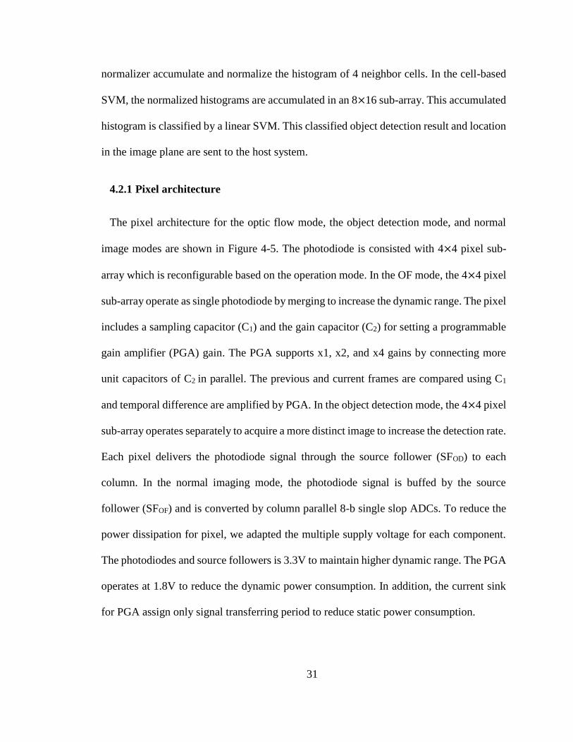
4.2.1 Pixel architecture
The pixel architecture for the optic flow mode, the object detection mode, and normal
image modes are shown in Figure 4-5. The photodiode is consisted with 4×4 pixel sub-
array which is reconfigurable based on the operation mode. In the OF mode, the 4×4 pixel
sub-array operate as single photodiode by merging to increase the dynamic range. The pixel
includes a sampling capacitor (C1) and the gain capacitor (C2) for setting a programmable
gain amplifier (PGA) gain. The PGA supports x1, x2, and x4 gains by connecting more
unit capacitors of C2 in parallel. The previous and current frames are compared using C1
and temporal difference are amplified by PGA. In the object detection mode, the 4×4 pixel
sub-array operates separately to acquire a more distinct image to increase the detection rate.
Each pixel delivers the photodiode signal through the source follower (SFOD) to each
column. In the normal imaging mode, the photodiode signal is buffed by the source
follower (SFOF) and is converted by column parallel 8-b single slop ADCs. To reduce the
power dissipation for pixel, we adapted the multiple supply voltage for each component.
The photodiodes and source followers is 3.3V to maintain higher dynamic range. The PGA
operates at 1.8V to reduce the dynamic power consumption. In addition, the current sink
for PGA assign only signal transferring period to reduce static power consumption.

32
Figure 4-5 Reconfigurable pixel architecture
4.3 HOG based object detection core operation
The block diagram of the implemented chip-level object detection core is shown in
Figure 4-6. The embedded object detection circuits mainly consist of two parts: HOG-
based object detector, which extracts the HOG feature and classify the object based-on 2-
b spatial difference images, and the memory controller manages the SRAM memory for
storing the weight vector, temporal result for cell histogram, and SVM classification result,

33
which optimize the memory size and data bandwidth between HOG-based object detector
and embedded buffer memory.
Figure 4-6 Block diagram of object detection core
The processing of the object detection is as follows: (1) 2-b spatial difference comparators
generate the 2-b spatial difference imaging by comparing the neighboring pixel value; (2)
a LUT-based gradient orientation generator assign the magnitude and bin value based-on
2-b spatial difference image; (3) a cell histogram generator assembles the magnitude of
gradients corresponding to its 9 bins in an 8×8 pixel sub-array; (4) the accumulated
histograms are normalized with 4 neighbor cells; and (5) a linear SVM classifies the object
by 9-b normalized HOG features using cell-based pipeline operation.

34
4.3.1 2-b spatial difference image and LUT-based orientation assignment
operation
In this sensor, we employed the 2-b spatial difference image to reduce the ADCs power
dissipation and to decrease the hardware complexity and resource for followed signal
processing for HOG feature extraction. The HOG-based object detection shows the
consistent accuracy performance even if the image resolution is decreased from 8 bit to 5
bit in Figure 4-7. However, the accuracy is dramatically starting to reduce when the image
resolution is under 5 bit. To overcome this accuracy degradation and reduce the ADC
power dissipation, we proposed the 2-b spatial difference images. The 2-b spatial
difference comparators extract column-parallel 2-b spatial difference image in the object
detection core block. By comparing between neighboring the pixel output values, 2-b
spatial difference image generates the positive edge and negative edge from input image.
The HOG feature is a function of edge orientations. As the result, the meaningful HOG
features are located at the edge of the object. The encoded image preserves the edge
information, which can help provide robust performance without high resolution ADCs.
Table 4-1 shows the pixel codes encoded from 2-b spatial difference conditions. In this
work, we used LUT-based orientation assignment to avoid complicated digital
implementation to extract the bin and magnitude of the gradient, which would consume
huge area and power.
Table 4-2 shows a table for bin and magnitude assignment. We assign positive and
negative edges to separate bins even though they may have the same gradient angles to
overcome the constraints from low-resolution spatial difference images. Figure 4-7 shows
the detection accuracy and normalized ADCs power dissipation. Instead of the 8-b
35
resolutions images, 2-b resolution image can reduce the ADCs power by 50× due to less
switching of single-slope ADCs operation. However, the accuracy is decreased to 75%.
Converting the input image to 2-b spatial difference image and using the customized LUT-
based orientation assignment achieves a 15% accuracy improvement in Figure 4-7. In
addition, 2-b spatial difference image technique can reduce 75% SRAM memory size for
the input buffer memory of the object detection core.
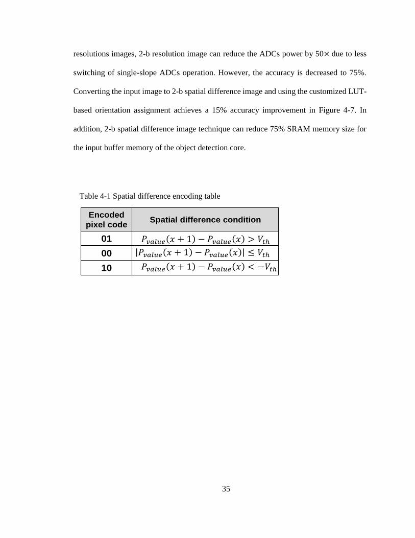
Table 4-1 Spatial difference encoding table
Encoded
pixel codeSpatial difference condition
01
00
10

36
Table 4-2 LUT-based Orientation assignment
Encoded
Bin Number
Encoded
Magnitude
0 0 0 0
1 0 1 1
1 1 3 5
0 1 5 1
-1 1 7 5
2 0 0 3
2 2 2 7
0 2 4 3
-2 2 6 7
-1 0 8 1
-2 0 8 3

37
(a) Pixel resolution (bit) versus detection precision (%)
(b) Normalized ADCs power versus detection rate precision (%)
Figure 4-7 Detection rate precision versus pixel resolution and normalized ADCs power

38
4.3.2 Cell-based SVM classification operation
Figure 4-8 depicts the SVM classification architecture. It consists of 128 processing
elements (PE) to support cell-based pipeline operation. In this work, linear SVM classifiers
are used for object detection with HOG features. The bit-width of the SVM weights is 4-b
singed fixed-point to reduce both the memory size and bandwidth instead of high resolution
floating point value [24]. The normalized HOG feature bit-width is 9-b signed fixed-point
to preserve the detection accuracy. The extracted normalized HOG feature of each cell is
once used to acquire the classification result, which is never stored or reused. Each PE is
consisted with one multiplier and one adder to compute and accumulate the partial dot
product of two values of HOG feature and the SVM weights. Figure 4-9 shows the cell-
based pipeline operation for the SVM classifier. The cell-based pipeline operation is
conducted as follows.
1) A cell histogram (9 bins) is generated from LUT-based gradient orientation
generator in a raster scan order.
2) When cell histogram generation reaches to a block level, block-level histogram
is normalized with 4-neighbor cell histograms (9-bins×4-cells×9-b).
3) The normalized HOG features (36 × 9-bit) and SVM weights (4-bit)
corresponding to each window are multiplied and accumulated at each PE.
4) The 29-bit temporal accumulated results are stored for each corresponding
window.
By storing the temporal accumulation results (29-b), instead of final normalized HOG
features (36×9-b) for a predefined window (128×36×9-b). Instead of storing whole 9-bit
normalized HOG feature for computing window classification, this cell-based pipeline
operation reduces the overall memory size by 75%.

39
Figure 4-8 SVM classification architecture

40
Figure 4-9 Cell-based pipeline operation for SMV classifier

41
4.3.3 Object Searching Scheme
Figure 4-10 shows the object search scheme. The false positive value is higher than
using high-resolution images due to the proposed 2-b spatial difference imaging. The object
is usually detected in multiple neighbor windows thanks to the resilience of the detection
algorithm. When an object is detected in the window, more searches are conducted for
neighboring windows. The system looks at the number of positive results among 4
windows. If the number of positive results is bigger than threshold, the system provides a
positive result. Using this search scheme, the false positive values can be decreased to <
6%.
Figure 4-10 Object search scheme to reduce the false positive

42
4.4 Implementation and Experimental Result
A prototype chip was fabricated using 0.18μm 1P4M process and has been fully
characterized. A chip micrograph is shown in Figure 4-11. The total chip size
6.20mm×4.00mm including I/O pads. The chip contains the reconfigurable pixel array, 2D
optic flow core, object detection core, a bias generator, a timing generator, and 8-b single-
slope ADCs for the normal image mode. Four embedded SRAMs are integrated to store
the 2D time-stamp array, buffer memory for the object detection core, and HOG weight
coefficients.
6.20 mm
4.0
0 m
m
Figure 4-11 Chip micrograph

43
4.4.1 2D optic flow estimation and object detection result from real moving object
The captured 2D optic flows and object detection result from the fabricated device are
shown in Figure 4-12. To demonstrate the performance and feasibility in an actual NAV,
we tested 3 cases: an object in spiral-up motion, a rotating fan, and a walking person. The
rotating fan was located in front of the resolution chart to confirm that proposed sensor
extract the optic flow under the complicated background patterns. The fan was rotating
with the speed of 65rpm; the sensor was capturing the flow at the frame rate of 60fps. The
result shown in Figure 4-12 (a) is the accumulated optic flow for 2 seconds. We tested the
spiral-moving object in order to verify the sensor, which can capture 3D moving object to
confirm the feasibility in the real situation for the actual NAVs operation. Red arrows
indicate the actual trajectory and black arrow represent the estimated optic flow from the
sensor in Figure 4-12(b). The sensor was capturing the optic flow at the frame rate of 30fps.
To demonstrate the proposed hybrid operation mode, which provide both the optic flow
estimation for navigating and object detection to classify the interesting object, the walking
person test pattern is measured. The sensor generates optic flow during the navigation
period. When the person is identified at object detection mode, the location of the object is
also reported. In Figure 4-12(c), the green arrow indicated the estimated optic flow form
walking person and yellow dot rectangle represent the location of the object where the
sensor classify as the person. The sensor was capturing the optic flow at the frame rate of
29 fps and classify the object at the 1 fps in the image.

44
(a) Spiral moving up object: captured @ 30fps
(b) Rotating fan: 65rpm @ 60fps (c) Walking person and object detection @ 30fps
Figure 4-12 Measured 2D optic flows of moving objects and object detection for a
walking pedestrian

45
4.4.2 Object detection accuracy test
In order to verify the performance of the integrated object detection in a real situation
with a variety of scenes, we used test image sets from the INRIA data base [25]. The
embedded SVM identifies the object and generates an 1-b output of the detection result
and location of the classified object. In order to classify the object, pre-trained weight
models have to be loaded in the object detection core SRAM. To extract weight models, a
large number of images are required as a training image set, which include both positive
and negative images. In this work, we used a linear SVM for training and employed
MATLAB for the classifier. However, the proposed object detection used 2-b spatial
difference image and customized gradient orientation assignment. We encoded 1000
images (500 positive, 500 negative) to 2-b spatial difference images and trained based on
proposed customized gradient orientation assignment. We tested 200 test images (100
positive, 100 negative) for evaluating detection. Experiments have shown 84% detection
rate.
4.4.3 Performance summary and comparison
The performance of the sensor is summarized in Table 4-3. We achieved a 29.94 µW in
the optic flow extraction mode at 30 fps and 2.18 mW in object detection mode at 30 fps,
respectively. In the hybrid operation mode (optic flow @ 29 fps and object detection mode
@ 1 fps), we achieved 101.61 µW. This result indicates proposed vision based navigating
operation can conduct more complicated mission with very low power overhead budget.
In order to verify the performance of embedded object detection, we tested 200 pedestrian
images from the INRA dataset [25]. The test result shows 84% detection rate. The relative

46
low object detection rate can be increased up to 96% by swarming NAVs in collaborative
action [3]. For the comparison of the power consumption, power Figure of merit (FOM) is
used [6], [27]. The power FOM is defined as the power normalized to the number of pixels
and the frame rate. Table 4-3 shows the power FOM and the key parameters comparison
with previous works. The proposed sensor achieved the low power FOM to estimate 2D
optic flow comparing pure analog or pure digital approaches. Comparing the previous
HOG object detection processor, proposed object detection core shows similar FOM even
if we integrate together image sensor and object detection core. In addition, the single chip
vision-based navigation sensor, which provide both object detection and 2D optic flow, is
the first attempt to minimize payload and power dissipation for NAVs.
Table 4-3 Chip characteristics

47
Table 4-4 Performance comparison with previous works
[46] [51] [63] [64] This work
Optic
Flow
Estimation
Technology N/A 0.5 µm 65nm 65nm 0.18µm
Processor Vertex
Pro2 N/A N/A N/A N/A
Pixel array N/A 19 x 1 N/A N/A 64 x 64
Pixel
size[um] N/A 112x257.3 N/A N/A 31 x 31
Optic Flow 2D
digital
1D WFI
Analog N/A N/A
2D Mixed
Mode
Total
Power
>50 mW
@30fps
42.6 µW
@1kHz N/A N/A
30 µW
@30Hz
FOM
[nJ/Pixel] 73 2.2 N/A N/A 0.244
Object
Detection
Core
Spatial
Resolution N/A N/A
1920 x
1080
1920 x
1080 256 x 256
Voltage N/A N/A 0.7 V 0.77V 1.2V
Frame rate N/A N/A 30 fps 30 fps 30 fps
Detection
algorithm N/A N/A
HOG +
SVM
HOG +
SVM
Customized
HOG + SVM
FOM
[nJ/pixel] N/A N/A 1.35 0.94 1.11
4.5 Summary and chapter conclusion
In this chapter, a vision based navigation sensor with embedded object detection and
2D optic flow extraction for NAVs has been introduced. Instead of transmitting a video
stream of images to host system to navigate the NAVs, the sensor provides the optic flow
information to support autonomous operation of NAVs by detecting the obstacle and
estimating the self-status of NAVs. The sensor switches the mode to find the target object,
which can provide crucial information to conduct missions of NAVs, and transfers the
object detection results. By providing optic flow estimation and object detection result,
NAVs can significantly reduce the power dissipation to transmit data to the host system.
We have employed 2-b spatial difference image, LUT-based orientation assignment, and

48
cell-based SVM to reduce the power dissipation, hardware resource, and memory size. To
support object detection and optic flow extraction, the pixel array is reconfigured for optic
flow estimation (64×64) and object detection (256×256). The sensor integrates the 2D
time-stamp-based optic flow estimation core, which is developed for efficient
implementation of bio-inspired time-of-travel measurement in the mixed-mode circuits [5].
We accomplished 272.49 pJ/pixel, the smallest power reported up to date, in hybrid
operation of optic flow extraction and object detection.

49
Chapter 5
CMOS image sensor with embedded mixed-mode convolution neural network for
object recognition
5.1 Introduction
Recently a neural network has made a significant progress with the deep learning
algorithms in the field of machine learning. Especially, convolutional neural networks
(CNNs) are consistently expanding their applications in computer vision, self-driving cars,
entertainment and speech processing [65]-[67]. One of the reasons for this recent attention
has been indebted to the ever-more increased computing power through the development
of multicore CPU's, GPU's, and even clusters of GPU's. These multicore processors allow
for training and evaluating larger networks. In addition, deep learning algorithms and the
new architectures of neural network contribute to pushing the state-of-the-art performance
[67]-[69]. Figure 5-1 shows the recent convolution neural networks (CNN) complexity and
ImageNet Large Scale Visual Recognition Challenge (ILSVRC) top 5 object recognition
error rate. The ResNet achieve 3.6% error rate which is lower than the error rate of the
human availability (5%). To achieve this performance, ResNet requires 20 times floating-
point operations and depth of networks. In addition, the number of weight also increased
2.5 time comparing with AlexNet. This complexity of the recent CNN lead higher
computing power. The increase in computing power inevitably leads to high power
dissipation. The high power consumption may not be a big concern for training because it

50
can be done in a big computer cluster. But it becomes problematic when the neural network
is used to evaluate the contents in an energy-limited mobile hardware, for example,
smartphones, smart glasses and other wearable devices. Huge power dissipation will
shorten the operation time of mobile and wearable devices.
Figure 5-1 CNN complexity and ILSVRC top 5 object recognition error rate
Recently, multicore GPU approaches have achieved a significantly enhanced
accuracy in computer vision. However, this conventional multicore GPU approach suffers
from high power dissipation (100W) [70]. To overcome this, several low-power CNN
ASICs have been developed by exploiting data reuse techniques, data-and-filter sparsity,
and dynamic-voltage-accuracy scaling [71-72]. However, these ASICs require external
high-bandwidth memory where the input images and intermediate results from image
processing should be stored, as shown in Figure 5-2 (a). These extra components result in
high power dissipation especially from the hi-bandwidth data transfer between the memory

51
and the processor. Recently, the integration of image sensing arrays and processing units
together on chip has shown promising result in low-power algorithmic imagers [11-13].
In this chapter, we propose a high energy-efficient CNN imager, in which the initial
convolution layers are effectively implemented in a mixed-mode signal domain by directly
processing analog image signals from the image pixel array and converting the result to
digital signals for the late-stage convolution layers, as shown in Figure 5-2(b). The
proposed CNN imager can effectively reduce the memory and computing power for the
early convolution layers, which require highest computing power among the entire neural
network layers [77].
(a) Conventional CNN imaging system
(b) Proposed low-power CNN real-time imager
Figure 5-2 (a) Conventional CNN imaging system, (b) Proposed low-power CNN real-time
imager with the mixed-mode MACs
This chapter is organized as follow. The CMOS image sensor embedded mixed-mode
neural network architecture is covered in the chapter 5.2. In the chapter 5.3, the main circuit
blocks and the adopted (used) circuit design techniques for realizing the architecture are

52
described in details. The chapter 5.4 presents the measurement results. Finally, the chapter
5.5 states the conclusions of this chapter.
5.2 Circuit architecture
Figure 5-3 shows the top level architecture of the high energy-efficient CNN imager.
The proposed system is consisted of a pixel array, mixed-mode MACs, rectified linear unit
(ReLU), analog memory, maximum pooling layer, and ADCs for converting mixed-signal
result of MACs to digital format. First, the 4T pixel array integrates photocurrent in each
pixel during given exposal time. The individual pixel values are transferred to a column-
parallel correlated double sampling (CDS) to suppress the reset and fixed pattern noise,
which is induced by each pixel. The analog image signals which is suppressed the noise by
CDS are then transferred to a column-parallel mixed-signal MACs in a rolling shutter
fashion. The column-parallel mixed-mode MACs process the convolution operation in the
analog-digital mixed-mode signal domain. After conducting the MACs operation, the
results are stored in analog and digital memory. The ReLU is located in front of the MACs.
Typically, the ReLU is placed after the MACs in the conventional neural network systems.
When the input value of MACs is negative, MACs process is skipped to save power
dissipation. Each convolution layer in the neural network is processed in a pipeline mode.
In the last stage, a column-parallel ADC converts the convoluted results to digital signals.
Consequently, the column-parallel mixed-mode MACs and the pipeline operation allow to
achieve real-time imaging at low-power operation.

53
Figure 5-3 CMOS image sensor architecture with embedded convolution neural network
algorithm
5.3 Circuit implementation
5.3.1 Mixed-mode MAC architecture
Figure 5-4 shows the proposed mixed-mode MAC architecture. The proposed
MACs consist of a multiplier, an accumulator, and an MAC controller. This mixed-mode
MACs employs a floating-point arithmetic. The significand and exponent are provided

54
from the analog and digital memory which stores the intermediate results calculated from
the previous layer. The analog value is multiplied with a weight (7b) for convolution
operation by the multiplier. The multiplied value is accumulated in the integrator. When
the exponents between the input value and MACs are different, the MAC controller
matches the exponent value by adjusting the gain of the integrator. Figure 5-4 shows the
example of operation, For example, if the input exponent is 1 and the MAC’s exponent is
1, the accumulator integrated the multiplied value from multiplier. When input exponent
value is smaller than stored accumulator exponent value, accumulator gain controller
adjusts the overall gain of the integrator to 0.5 to match the exponent value. In addition,
when the VOUT level is higher than the threshold level with the comparator (COMP1), the
integrator samples VOUT and divide it by 2 to prevent the overflow of the analog value.
Simultaneously, the MAC’s exponent value is increased. This mixed-mode folding process
can increase the dynamic range without sacrificing the resolution.
Figure 5-4 Proposed mixed-mode MAC architecture

55
Figure 5-5 Proposed mixed-signal accumulator operation
5.3.2 Passive charging sharing based multiplier
Figure 5-5 shows the proposed passive charge redistribution multiplier. In the
previous literature, a switched-capacitor multiplier was introduced [74]. However, this
implementation requires the amplifiers which consume significant static current. To
overcome this problem, we adapt the passive charge-redistribution multiplier for mixed-
mode computing. However, a switched-capacitor multiplier require the wide bandwidth
buffer due to the large capacitor bank. To overcome this problem, this switched-capacitor
multiplier enjoy the split capacitive DAC array architecture. By deploying split capacitive
DAC array architecture, effective input capacitance of the switched-capacitor multiplier is
reduced by 5.5 times. The operation of multiplier is divided into two steps: sampling phase
and charge-redistribution phase. First, the VSIG is sampled only at the bottom of capacitors
where the binary weight (W) bits are 1. The charge stored on a capacitor bank is given by:

56
𝑄𝑏 = 𝑊 × 𝐶 × 𝑉𝑆𝐼𝐺.
Next, the bottom of capacitors are connected to VCM. As a result, the stored charges during
sampling phase are redistributed. After charge redistribution, the VOUT is given by:
𝑉𝑂𝑈𝑇 = −𝑊
(2𝐵)𝑉𝑆𝐼𝐺
, where B is the number of magnitude bits. Figure 5-5 shows the operation of the passive
charge-redistribution multiplier for example when W and B are 64 (1000100b) and 7,
respectively.
Figure 5-6 Operation of the passive charge-redistribution multiplier. In this example,
W=7(1000100b), and B=7

57
5.3.3 Energy-efficient algorithm optimization for CNN
During the CNN operation, to improve training and evaluation efficient, ReLUs are
deployed between each neural network layer. Figure 5-6(a) shows conventional CNN
operation. First, MAC conduct convolution operation between input image values and
weight values. After convolution operation, ReLU activate output value of the MAC. After
activating through ReLU, the negative value assign as 0 value and positive values are
preserved. The memory unit store the result of ReLU. Followed MAC layer process the
convolution operation by loading the stored value in memory. Figure 5-6(b) shows the
proposed energy efficient CNN operation. At the first MAC operation, MAC process
convolution between input image values and weight value. Comparing with conventional
CNN operation, proposed energy efficient processing store the result of MAC without
filtering ReLU functionality. The around half of the distribution of MAC output value is
negative due to the nature of weight value distribution. At 2nd neural network layer, MAC
and ReLU functionality easily can be merged together by skipping convolution operation
when the negative layer 1 neural network value arrive as input of MAC operation. During
this MAC operation, the around half of MAC operation could be skipped thanks for nature
of weight values distribution.

58
(a) Conventional CNN operation
(b) Proposed energy efficient CNN operation
Figure 5-7 Proposed hardware and energy efficient CNN operation

59
Figure 5-8 shows the 2nd mixed-signal MAC architecture to support the proposed
energy efficient CNN operation. First, Comp1 compare between VCM (zero value) and
loaded value from previous layer output memory. If loaded value is bigger than VCM,
EN signal is enable and batch the weight value and process 2nd MAC operation. When
the loaded value from previous layer memory is smaller than VCM (zero value), EN signal
is disabled, which mean the MAC block will not process the coevolution operation.
Obviously, we can turn off the 2nd MAC block and do not need to load weight value
form external memory unit during around the half of MAC operation time, thanks to the
nature of CNN weight value distribution. This approach can reduce the half of power
dissipation of 2nd layer MAC operation and IO power dissipation to load weight value.
Figure 5-8 2nd layer MAC operation to support proposed CNN scheme
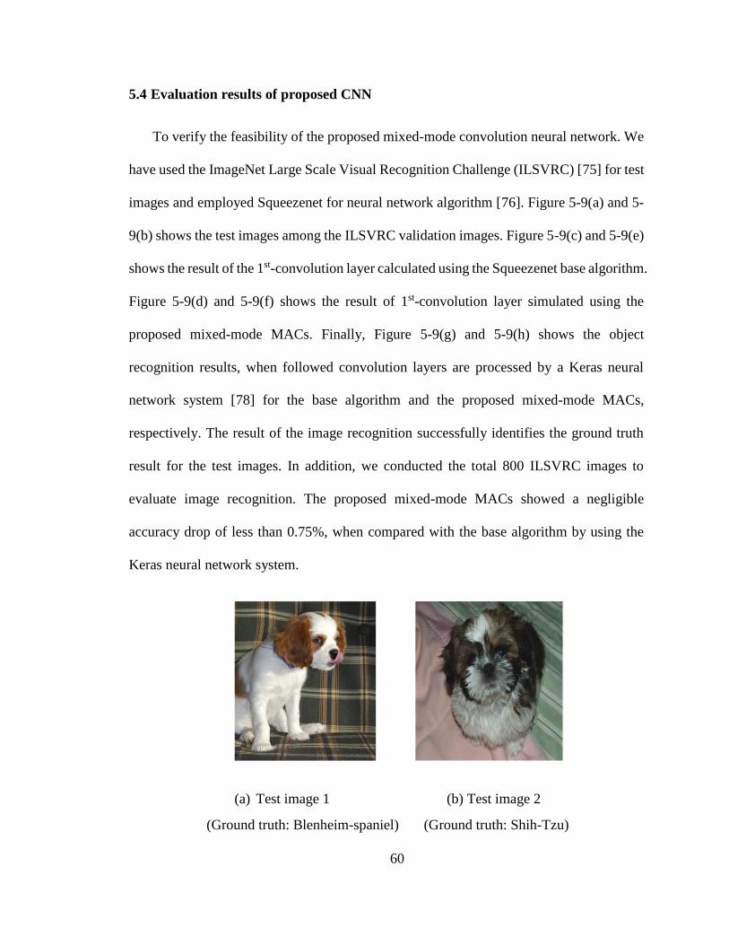
60
5.4 Evaluation results of proposed CNN
To verify the feasibility of the proposed mixed-mode convolution neural network. We
have used the ImageNet Large Scale Visual Recognition Challenge (ILSVRC) [75] for test
images and employed Squeezenet for neural network algorithm [76]. Figure 5-9(a) and 5-
9(b) shows the test images among the ILSVRC validation images. Figure 5-9(c) and 5-9(e)
shows the result of the 1st-convolution layer calculated using the Squeezenet base algorithm.
Figure 5-9(d) and 5-9(f) shows the result of 1st-convolution layer simulated using the
proposed mixed-mode MACs. Finally, Figure 5-9(g) and 5-9(h) shows the object
recognition results, when followed convolution layers are processed by a Keras neural
network system [78] for the base algorithm and the proposed mixed-mode MACs,
respectively. The result of the image recognition successfully identifies the ground truth
result for the test images. In addition, we conducted the total 800 ILSVRC images to
evaluate image recognition. The proposed mixed-mode MACs showed a negligible
accuracy drop of less than 0.75%, when compared with the base algorithm by using the
Keras neural network system.
(a) Test image 1 (b) Test image 2
(Ground truth: Blenheim-spaniel) (Ground truth: Shih-Tzu)

61
(c) Squeezenet base software result for test image 1 (1st convolution)
(d) Proposed mixed-mode MACs result for test image 1 (1st convolution)

62
(e) Squeezenet base software result for test image 2 (1st convolution)
(f) Proposed mixed-mode MACs result for test image 2 (1st convolution)

63
(g) Test image1 recognition result (h) Test image 2 recognition result
Figure 5-9 Object recognition simulation result
5.5 Implementation and Experimental result
A prototype chip was fabricated using 90nm 1P4M back-side illumination (BSI)
CMOS image sensor process and has been fully characterized. A chip micrograph is shown
in Figure 5-10. The total chip size 3.70mm×4.50mm including I/O pads. The chip contains
the 452 x 304 pixel array, row scanner, CDS, column parallel mixed-mode MAC for layer
1 and 2, mixed-signal memory array, and 8-b single-slope ADCs for the normal image
mode and CNN result. Between each layer, there is maximum pooling layer to decrease
the dimension of the output MAC layer.

64
Figure 5-10 Die microphotograph of CMOS image sensor with embedded mixed-mode
convolution neural network
5.5.1 Experimental result
To verify the proposed mixed-mode MAC operation, we measure the relative
accuracy for each output quantization bit. Figure 5-11 shows the relative accuracy of
simulation and experimental result as a function of the number. Simulation result shows 1%
relative accuracy drop when we assign 6 bits for significand and 2 bits for exponent. In
experimental result, we used 2 bits exponent and measure relative accuracy varying number
of bit for significand. At experimental result, it shows the similar result comparing with
simulation result. At 6 bits for significand and 2 bits for exponent, relative accuracy only
shows the 1% relative accuracy drop. In addition, to verify the proposed mixed-mode
floating point arithmetic, we measured the relative accuracy without evaluating the

65
exponent value. The result shows the dramatically drop of relative accuracy even if the
output quantization bits is 8 bits. This is because intermediate output value of MAC during
convolution operation is saturated.
Figure 5-11 Relative accuracy of simulation and experimental result as a function of the
number or output quantization bits.
Figure 5-12 shows the measured result of CNN evaluation result. We can
successfully capture the image from normal image mode from test image. Even if the
captured image has a column fixed noise due to the mismatch of source follower which
followed pixel. After evaluating 2 layers from manufactured chip, Figure 6-11(c) shows
the evaluation result with predicted bounding boxes. Figure 6-11(d) and (e) shows the
intermediated first and second layer result (16 out of 64 layers). Still some of layer is
suffered from CFPN which is induced by pixel readout block mismatch. The activated
result reflect relevant activation result from each weight layer. The detection Figure of
merit, intersection over union (IOU), which measures the overlap ratio between the ground

66
truths and predicted bounding boxes, is shown in each image. If IOU is greater than 50 %,
the detection is regarded as successful [83].
(a) Test image (b) Captured image mode (c) CNN evaluation result
(c) The first layer output (shown only 16 out of 64 channels) from test image with
SqueezeDet

67
(d) The second layer output (shown only 16 out of 64 channels) from test image with
SqueezeDet
Figure 5-12 Extracted the intermediate result of CNN layers with proposed relative
accuracy of simulation and experimental result as a function of the number or output
quantization bits.
The evaluation images from the customized dataset are used to test the proposed
mixed-signal MAC architecture. Figure 5-13(a) shows the example of evaluation images
with the predicted bounding boxes, using fully digital processing of SqueezeDet through
software. Figure 5-13(b) shows the evaluation result using the mixed-signal MAC test
module with gray images. In this test, we directly provide the gray image data to MAC
module and could verify that the eye-nose regions were successfully detected with the

68
proposed mixed-signal MAC with IOU higher than 60%. The evaluation result with
fabricated chip is demonstrated in Figure 5-13(c). Even though the captured image
through pixel arrays have CFPN due to column readout mismatch, the IOU result could
achieve higher than 60%.
(a) IOU evaluation result with color image through software(bounding box prediction
result)
(b) IOU evaluation result with gray image through test module(MAC)
(c) IOU evaluation result with fabricated chip(bounding box prediction result)
Figure 5-13 Chip evaluation result and comparison of the IOU evaluation

69
5.5.2 Performance summary and comparison
The performance of the sensor is summarized in
5-1. We achieved a 7.15 mW in the normal image mode at 10 fps and 9.89 mW in CNN
object recognition mode at 10 fps, respectively. We achieved 5.2 nJ/pixel in the normal
image mode and 4.46 GOPS/W in CNN object recognition mode, respectively. This result
indicates proposed image sensor with embedded mixed-signal convolution neural network
can conduct more power limited environment. In order to verify the performance of
embedded neural network, we tested 100 images and evaluated IOU [83]. The test result
shows 1% relative accuracy drop (IOU>60%). Even though the relative accuracy shows
relevant result, the difference between IOU result from software and fabricated chip is not
negligible. This result might be come from the pixel array readout mismatch and reference
voltage buffer. We could overcome this problem by deploying larger dimension transistors
for these blocks. For the comparison of the power consumption, power Figure of merit
(FOM) is used [6], [27]. The power FOM is defined as the power normalized to the number
of pixels and the frame rate. In addition, to compare of the power efficiency, GOPS/W is
used. That FOM is defined as the GOPS normalized to the power.

70
Table 5-1 Performance summary of this works
5.6 Summary
In this chapter, the new CMOS image architecture embedded with convolutional
neural network which is implemented by mixed-mode MACs. The proposed scheme
supports the pipeline operation to achieve real time operation of the modified floating-point
arithmetic at low power. Power dissipation was significantly reduced by adapting a passive
charge redistribution scheme in the multiplier implementation. We have extensively
conducted simulations to verify the feasibility of the proposed architecture. The simulation
results shows that proposed mixed-mode MACs can evaluate the object recognition task
without significant accuracy drop (<0.75%). We measured relative accuracy with IOU
evaluation and achieved only 1% relative accuracy drop for IOU evaluation. Consequently,

71
the column-parallel mixed-mode MACs and the pipeline operation allow to achieve real-
time imaging at low-power operation. The system operates at 5.2 nJ/pixel in normal image
extraction mode and at 4.46 GOPS/W in CNN operation mode, respectively.

72
Chapter 6
Concurrent energy Harvesting and imaging sensor system for distributed IoT
sensor with embedded-learning algorithm
6.1 Introduction
In this chapter, we introduce the energy harvesting approach for CMOS image
sensor system with embedded machine-learning algorithm. CMOS image sensors have
been widely used for distributed IoT sensor nodes for continuous monitoring of
environments due to their small form factor and low power consumption [12]. These
distributed IoT sensor nodes should be able to operate and cover comprehensive,
unreachable areas under a limited energy source. Especially, CMOS image sensor has
embedded machine-learning algorithm shows additional power dissipation due to
evaluated algorithm. To further extend the lifetime of the distributed sensor nodes, several
potential energy harvesting methods has been explored, including vibration, radiation,
solar energy, etc. Among these, photovoltaic energy harvesting showed a high potential to
support remotely-distributed IoT image sensors due to its high energy harvesting efficiency
and compatibility with conventional CMOS processes [79-82]. The pixels in [80-81]
adopted a reconfigurable PN-junction diode that switches between photodiode
(photocurrent generation) and the photovoltaic (solar cell) operations, and showed a
promising result. However, this pixel could not provide continuous video images due to
mode switching. To overcome this limitation, the two separate photodiodes were

73
implemented side-by-side for imaging and photovoltaic operations simultaneously [81-82].
However, this approach inevitably leads to a low fill factor and a large pixel size.
In this chapter, we propose a self-sustainable CMOS image sensor with concurrent
energy harvesting and imaging without additional area penalty of photodiodes and the
degradation of energy-harvesting efficiency.
6.2 Circuit architecture
The proposed CMOS image pixel utilized two vertically-stacked diodes realized in
the same pixel: one for hole-accumulation photodiode (P+/NWELL) inside the N-well and
the other for photovoltaic energy harvesting diode (NWELL/PSUB) below the N-well. In
addition, a delta-reset sampling scheme is employed to suppress the fixed pattern noise
(FPN) using a bi-directional ramp generator.
Figure 6-1 depicts the overall pixel architecture and a system block diagram. Each
pixel consists of a photodiode (DP1) for imaging and a photovoltaic diode (DP2) for energy
harvesting. Contrary to typical CMOS image sensors, these two diodes, DP1 and DP2,
accumulate holes, not electrons. Holes generated by incident light are drifted to and
collected in the anode of each diode. DP1 forms a 3T pixel with MP1, MP2 and reset transistor
(MP3), accumulating photocurrent in VPD during integration time. DP2 continuously
harvests energy from illuminated light without any interruption, producing the
photovoltage at VEH. Column-parallel 8-b single-slope (SS) ADCs operate in the delta-
reset sampling mode with a bi-directional ramp signal generator and an 8-b counter for
image capturing at low power.

74
Figure 6-1 Energy harvesting image (EHI) sensor architecture
6.3 Pixel architecture
Figure 6-2 (bottom) shows the proposed pixel architecture. The stacked vertical
junction structure of P+/NWELL/PSUB forms the two diodes: DP1 (P+/NWELL) and DP2
(NWELL/PSUB). The P+ diffusion layer (anode of DP1) is connected to the drain of reset
transistor (MP3) and the gate of input transistor (MP1), which is a part of the comparator
circuit for SS ADCs. Peripheral transistors for pixel operation (MP1, MP2 and MP3) are
designed by PMOS transistors inside the N-well. This results in a high fill factor of 47%
for DP1. Moreover, the energy harvesting efficiency can be greatly enhanced by using the
entire N-well area realized by the NWELL/PSUB diode (DP2). DP2 can achieve a near perfect
fill factor (>94%) in a small pixel of 5um x 5um. In addition, it should be noted that the

75
amount of photo-generated charges are not only determined by the area of the diode but
also the depletion width. The PSUB and NWELL areas are lightly doped as compared to P+
or N+ regions. Therefore, a larger depletion width can be formed in DP2, resulting in a
higher energy harvesting efficiency. Figure 6-2 (top) shows the pixel cross-section and
readout circuit diagram. When the incident light reaches the depletion regions of DP1 and
DP2, the holes are generated and drifted to the anode of each diode. The accumulated holes
in DP2 are used for energy harvesting, supplying the photovoltage at VEH. The accumulated
holes in DP1 during the integration time will be read out for image captures, using the two
transistors in the pixel (MP1, MP2) with other two transistors in the column (MC1, MC2) as
a differential pair in the comparator for SS ADCs and sharing the COM node and SIG1
node in the same column.

76
Figure 6-2 Circuit diagram of the energy harvesting image sensor and the proposed pixel
structure

77
6.4 CMOS imager operation for energy harvesting and imaging modes
Timing diagram for imaging and energy harvesting is shown in Figure 6-3. When
the incident light starts generating holes, the voltage of energy harvesting node (VEH)
increases during the start-up phase. When VEH reaches to a trigger voltage, the external
energy harvest (EH) power management unit starts supplying power to the sensor circuits
and the image capture starts [6]. The image capture operation is conducted as follows: (1)
CNTRST signal resets the code of the counter to 256; (2) VRAMP starts decreasing to capture
the DP1 signal level (VPD); (3) when VRAMP reaches the DP1 signal level, the counter latched
the code corresponding to VPD; (4) after resetting the photodiode (DP1), VRAMP starts
increasing to detect the reset signal level of DP1; (5) when VRAMP reach the DP1 reset signal
level, the counter latch the code equivalent to (VSIG – VRST). By employing the bi-
directional ramp signal for delta-reset sampling operation, we can suppress the FPN, which
was mainly induced by variations and mismatches of MP3 and MP1.

78
Figure 6-3 Timing diagram of the image readout and energy harvesting circuits
6.5 Experiment results
Figure 6-4 shows the measured results: harvested open circuit voltage (VEH – VDC),
harvested power, and power dissipation of the sensor as a function of illumination levels.
When the illumination is higher than 1 klux, the harvested supply voltage can reach higher
than 0.33V, which is sufficient to start up and operate the external EH power management

79
unit [6]. The power management unit can generate 0.6V supply for the image sensor array
by boosting up from the harvested open circuit voltage of 0.45V. The harvested energy is
sufficient to continuously supply the required power of 3.9uW at 7.5fps of image capture
under 20 klux (normal daylight) and 10.08uW at 15fps under 50 klux(sunny daylight),
respectively.
Figure 6-4 Measured harvesting voltage, power, chip power consumption as a function of
illumination levels
Figure 6-5 shows the captured images from the fabricated prototype device in a 100
x 90 spatial resolution at 7.5fps and 15fps, respectively. In these images, the FPN (rms) is
suppressed from 9.2% to 3.8% under dark conditions by delta-reset sampling operation.
Nevertheless, column fixed-pattern noise (CFPN) is evident in the captured images. This
CFPN may result from Vth variations of MC1 in the comparator during SS ADCs operation.

80
The CFPN can be suppressed by adopting a larger transistor size of MC1 and/or by
employing a column gain controller for each column without significant increase of power
dissipation. Furthermore, the spatial resolution of the proposed imager is easily expandable
for self-sustainable imaging operation because the harvested power increases
proportionally to the area of the entire pixel array.
Figure 6-5 Test images of a U.S. hundred dollar bill at VDD = 0.6V
6.6 Summary and comparison
The performance comparison of the fabricated imager is summarized in Table 6-1.
We accomplished the Figure of merit (FOM) of 57.78pJ/pixel and 74.67pJ/pixel at 7.5fps
and 15fps in the image capturing circuits. We can harvest the power of 998pW/klux/mm2
from photovoltaic diodes. This gives the total FOM of -4.71pJ/pixel and -10.05pJ/pixel at
20 klux and 50 klux, respectively, demonstrating the self-sustainable image-capture
operation without battery. A prototype chip is fabricated using a 0.18µm CMOS process.

81
A chip micrograph is shown in Figure 6-6. In this chapter, we introduce a self-sustainable
CMOS image sensor with concurrent energy harvesting and imaging for CMOS image
sensor with embedded machine-learning algorithm at distributed sensor nodes environment.
The proposed CMOS image sensor utilized two vertically-stacked diodes realized in same
pixel: one for hole-accumulation photodiode and the other for photovoltaic energy-
harvesting diode. We demonstrated image capturing from batteryless self-sustained
operation. The sensor achieved a negative Figure of merit (FOM) of -13.9 pJ/pixel at 30
Klux (normal daylight) thanks to a high fill factor of 94% in the energy harvesting diode.
The proposed energy harvesting pixel structure can extend the lifetime for distributed
CMOS image sensor with embedded machine-learning algorithm and provide video stream
images without area penalty.
Figure 6-6 Energy harvesting CMOS image sensor chip photograph

82
Table 6-1 Performance summary and comparison table

83
Chapter 7 Summary and future work
7.1 Summary
The goal of this research is to provide the architecture, algorithm optimization, and
associated circuit for energy-efficient CMOS image sensor with embedded machine-
learning algorithms. In order to achieve this goal, it is important to address specific circuit
and architecture design challenges; minimizing hardware resource, reducing the data
bandwidth, and energy consumption while not compromising machine learning algorithm
performance. The three interdependent projects; embedded object detection sensor for a
vision based navigation system, CMOS image sensor with embedded mixed-mode CNN
for object recognition, and concurrent energy harvesting and imaging sensor system have
been carefully designed to accomplish this goal.
The embedded object detection sensor for a vision based navigation system was
designed using a 2-b spatial difference imaging, the customized LUT-based gradient
orientation assignment to reduce the data bandwidth and hardware resource and fabricated
in 0.18 µm CMOS process. The proposed system accomplished 272.49 pJ/pixel, the
smallest power reported up to date, in hybrid operation of optic flow extraction and object
detection.
Then, the CMOS image sensor with embedded mixed-mode CNN for object
recognition was built in the 90 nm CMOS Image sensor process to minimize the energy
consumption overhead for MAC operation, especially, in due to high speed clock. We

84
measured relative accuracy with IOU evaluation and achieved only 1% relative accuracy
drop for IOU evaluation. Consequently, the column-parallel mixed-mode MACs and the
pipeline operation allow to achieve real-time imaging at low-power operation. The system
operates at 5.2 nJ/pixel in normal image extraction mode and at 4.46 GOPS/W in CNN
operation mode, respectively.
For the sake of the overall system, not only for the energy usage efficiency, but the
additional energy source for the system is also considered. The pixel level concurrent
energy harvesting and imaging sensor system was developed to extend the lifetime for the
CMOS image sensor with embedded machine-learning algorithm. The sensor achieved -
13.9 pJ/pixel at 30 Klux (normal daylight), 94% FF for energy harvesting diode, and 47%
FF for imaging sensing diode. The proposed energy harvesting pixel structure can extend
the lifetime for distributed CMOS image sensor with embedded machine-learning
algorithm and provide video stream images without area penalty.
7.2 Future work
Although several contributions have been made in this research to realize the CMOS
images sensor with embedded machine-learning algorithm, there are still some areas of
improvements in the design. For further improvements and future work the followings are
suggested.
An I/O data compression circuits for weight values are necessary. Even though the
fabricated sensor evaluated machine-learning algorithm in chip level, the power
consumption for loading the weight values, which is required to evaluate machine-

85
learning algorithm, was not negligible due to the large weight values data movement.
The data compression for weight value can reduce I/O power consumption significantly.
An integration of the proposed energy harvesting pixel structure with the CMOS image
sensor for the embedded machine-learning algorithm is necessary. The energy
harvesting CMOS image sensor was designed and fabricated independently and its
performance was measured separately. To realize the complete system, the proposed
pixel structure should be on a single die with the embedded machine-learning algorithm.
In addition, the power convertor to provide imager system is required.
To evaluate fully neural network algorithm in CMOS image sensor system, FCC and
followed functionality block for CNN should be developed. Currently, early
convolution layer is developed with embedded convolution circuit. Followed
convolution layer require higher resolution comparing of early convolution layer. This
lead the energy efficient digital approach for followed convolution layer and FCC layer.
To further verify vision based navigation system, we require integrating fabricated
system to NAV. In addition, to navigate the NAV system, digital signal processing
(DSP) units have to be integrated together to provide information to control the NAV
system.

86
BIBLIOGRAPHY
[1] E. R. Fossum, “CMOS image sensors: electronic camera-on-a-chip,” IEEE
Transactions on Electron Devices, vol. 44, no. 10, pp. 1689-1698, 1997.
[2] //www.jpl.nasa.gov/news/[online]
[3] Funatsu, Ryohei, Steven Huang, Takayuki Yamashita, Kevin Stevulak, Jeff
Rysinski, David Estrada, Shi Yan et al. "6.2 133Mpixel 60fps CMOS image sensor
with 32-column shared high-speed column-parallel SAR ADCs." In Solid-State
Circuits Conference-(ISSCC), 2015 IEEE International, pp. 1-3. IEEE, 2015.
[4] Kobayashi, Masahiro, Yusuke Onuki, Kazunari Kawabata, Hiroshi Sekine, Toshiki
Tsuboi, Yasushi Matsuno, Hidekazu Takahashi et al. "4.5 A 1.8 e rms− temporal
noise over 110dB dynamic range 3.4 µm pixel pitch global shutter CMOS image
sensor with dual-gain amplifiers, SS-ADC and multiple-accumulation shutter." In
Solid-State Circuits Conference (ISSCC), 2017 IEEE International, pp. 74-75. IEEE,
2017.
[5] Xu, Ruoyu, Wai Chiu Ng, Jie Yuan, Shouyi Yin, and Shaojun Wei. "A 1/2.5 inch
VGA 400 fps CMOS image sensor with high sensitivity for machine vision." IEEE
Journal of Solid-State Circuits 49, no. 10 (2014): 2342-2351..
[6] Seo, Min-Woong, Tongxi Wang, Sung-Wook Jun, Tomoyuki Akahori, and Shoji
Kawahito. "4.8 A 0.44 e− rms read-noise 32fps 0.5 Mpixel high-sensitivity RG-less-
pixel CMOS image sensor using bootstrapping reset." In Solid-State Circuits
Conference (ISSCC), 2017 IEEE International, pp. 80-81. IEEE, 2017.
[7] A. El Gamal, H. Eltoukhy, "CMOS image sensors," Circuits and Devices magazine,
IEEE , vol.21, no.3, pp. 6-20, May-June 2005
[8] LeCun, Yann, Léon Bottou, Yoshua Bengio, and Patrick Haffner. "Gradient-based
learning applied to document recognition." Proceedings of the IEEE 86, no. 11
(1998): 2278-2324..
[9] Silver, David, Julian Schrittwieser, Karen Simonyan, Ioannis Antonoglou, Aja
Huang, Arthur Guez, Thomas Hubert et al. "Mastering the game of go without
human knowledge." Nature 550, no. 7676 (2017): 354.
[10] He, Kaiming, Xiangyu Zhang, Shaoqing Ren, and Jian Sun. "Deep residual learning
for image recognition." In Proceedings of the IEEE conference on computer vision
and pattern recognition, pp. 770-778. 2016..
[11] S. Park, J. Cho, K. Lee, and E. Yoon, "7.2 243.3 pJ/pixel bio-inspired time-stamp-
based 2D optic flow sensor for artificial compound eyes," In Solid-State Circuits
Conference Digest of Technical Papers (ISSCC), 2014 IEEE International, pp. 126-
127, 2014

87
[12] J. Choi, S. Park, J. Cho, and E. Yoon, "A 3.4-uW Object-Adaptive CMOS Image
Sensor with Embedded Feature Extraction Algorithm for Motion-Triggered Object-
of-Interest Imaging," IEEE Journal of Solid-State Circuits, vol. 49, no. 1 pp. 289-
300, 2014..
[13] K. Lee, S. Park, S. Park, J. Cho, and E. Yoon, "A 272.49 pJ/pixel CMOS image
sensor with embedded object detection and bio-inspired 2D optic flow generation
for nano-air-vehicle navigation," In VLSI Circuits, 2017 Symposium on, pp. C294-
C295, 2017.
[14] K. Lee, S. Park, S. Park, J. Cho, and E. Yoon, "A 272.49 pJ/pixel CMOS image
sensor with embedded object detection and bio-inspired 2D optic flow generation
for nano-air-vehicle navigation," In VLSI Circuits, 2017 Symposium on, pp. C294-
C295, 2017..
[15] Szegedy, Christian, Sergey Ioffe, Vincent Vanhoucke, and Alexander A. Alemi.
"Inception-v4, inception-resnet and the impact of residual connections on learning."
In AAAI, vol. 4, p. 12. 2017.
[16] Cristianini, Nello, and John Shawe-Taylor. An introduction to support vector
machines and other kernel-based learning methods. Cambridge university press,
2000..
[17] H. T. D.X.D Yang, A.E. Gamal, B. Fowler, “A 640x512 CMOS image sensor with
ultrawide dynamic range floating-point pixel-level ADC,” IEEE Journal of Solid
State Circuits, 1999..
[18] D. Kim, Y. Chae, J. Cho, and G. Han, “A Dual-Capture Wide Dynamic Range
CMOS Image Sensor Using Floating-Diffusion Capacitor,” IEEE Trans. Electron
Devices, vol. 55, no. 10, pp. 2590–2594, Oct. 2008..
[19] C. Lotto, P. Seitz, and T. Baechler, “A sub-electron readout noise CMOS image
sensor with pixel-level open-loop voltage amplification,” in 2011 IEEE
International Solid-State Circuits Conference, 2011, pp. 402–404..
[20] S. Kavadias, B. Dierickx, D. Scheffer, A. Alaerts, D. Uwaerts, and J. Bogaerts, “A
logarithmic response CMOS image sensor with on-chip calibration,” IEEE J. Solid-
State Circuits, vol. 35, no. 8, pp. 1146–1152, Aug. 2000. 0.
[21] S.-W. Han, S.-J. Kim, J. Choi, C.-K. Kim, and E. Yoon, “A High Dynamic Range
CMOS Image Sensor with In-Pixel Floating-Node Analog Memory for Pixel Level
Integration Time Control,” in Symposium on VLSI Circuits, Digest of Technical
Papers., 2006, pp. 25–26..
[22] T. Hamamoto and K. Aizawa, “A computational image sensor with adaptive pixel-
based integration time,” IEEE J. Solid-State Circuits, vol. 36, no. 4, pp. 580–585,
Apr. 2001..
[23] D. Stoppa, A. Simoni, L. Gonzo, M. Gottardi, and G.-F. Dalla Betta, “Novel CMOS
image sensor with a 132-dB dynamic range,” IEEE J. Solid-State Circuits, vol. 37,
no. 12, pp. 1846–1852, Dec. 2002..
[24] D. Stoppa, M. Vatteroni, D. Covi, A. Baschirotto, A. Sartori, and A. Simoni, “A
120-dB Dynamic Range CMOS Image Sensor With Programmable Power

88
Responsivity,” IEEE J. Solid-State Circuits, vol. 42, no. 7, pp. 1555–1563, Jul. 2007..
[25] “Complete Visual Networking Index (VNI) Forecast,” Cisco, June 2016.7.
[26] M. Price, J. Glass, and A. P. Chandrakasan, “A 6 mW, 5,000-Word Real-Time
Speech Recognizer Using WFST Models,” IEEE J. Solid-State Circuits, vol. 50, no.
1, pp. 102–112, 2015.
[27] R. Yazdani, A. Segura, J.-M. Arnau, and A. Gonzalez, “An ultra low-power
hardware accelerator for automatic speech recognition,” in MICRO, 2016..
[28] N. Verma, A. Shoeb, J. V. Guttag, and A. P. Chandrakasan, “A micro-power EEG
acquisition SoC with integrated seizure detection processor for continuous patient
monitoring,” in Sym. on VLSI, 2009..
[29] T.-C. Chen, T.-H. Lee, Y.-H. Chen, T.-C. Ma, T.-D. Chuang, C.-J. Chou, C.- H.
Yang, T.-H. Lin, and L.-G. Chen, “1.4_W/channel 16-channel EEG/ECoG
processor for smart brain sensor SoC,” in Sym. on VLSI, 2010.
[30] R. E. Schapire and Y. Freund, Boosting: Foundations and algorithms. MIT press,
2012.
[31] Y. LeCun, Y. Bengio, and G. Hinton, “Deep learning,” Nature, vol. 521, no. 7553,
pp. 436–444, May 2015.
[32] O. Russakovsky, J. Deng, H. Su, J. Krause, S. Satheesh, S. Ma, Z. Huang, A.
Karpathy, A. Khosla, M. Bernstein, A. C. Berg, and L. Fei-Fei, “ImageNet Large
Scale Visual Recognition Challenge,” International Journal of Computer Vision
(IJCV), vol. 115, no. 3, pp. 211–252, 2015.
[33] Y. LeCun, K. Kavukcuoglu, and C. Farabet, “Convolutional networks and
applications in vision,” in ISCAS, 2010.
[34] Y. LeCun, K. Kavukcuoglu, and C. Farabet, “Convolutional networks and
applications in vision,” in ISCAS, 2010.
[35] K. He, X. Zhang, S. Ren, and J. Sun, “Deep Residual Learning for Image
Recognition,” in CVPR, 2016.
[36] Floreano, Dario, and Robert J. Wood, "Science, technology and the future of small
autonomous drones," Nature 521, no. 7553, pp. 460-466, 2015.
[37] Uchida, Noriki, Noritaka Kawamura, Tomoyuki Ishida, and Yoshitaka Shibata,
"Proposal of Autonomous Flight Wireless Nodes with Delay Tolerant Networks for
Disaster Use," In Innovative Mobile and Internet Services in Ubiquitous Computing
(IMIS), 2014 Eighth International Conference on, pp. 146-151. IEEE, 2014.
[38] Gade, Shripad, and A. Joshi, "Heterogeneous UAV swarm system for target search
in adversarial environment," Control Communication and Computing (ICCC), 2013
International Conference on. IEEE, 2013.
[39] L. Petricca, Per Ohlckers, and Christopher Grinde, "Micro-and nano-air vehicles:
State of the art," International journal of aerospace engineering 2011 (2011).
[40] M. Blösch, S. Weiss, D. Scaramuzza, and R. Siegwart, "Vision based MAV
navigation in unknown and unstructured environments," In Robotics and
89
automation (ICRA), 2010 IEEE international conference on, pp. 21-28, 2010.
[41] J. Zufferey, A. Klaptocz, A. Beyeler, J. Nicoud, and D. Floreano, “A 10-gram
Vision-based Flying Robot,” Adv. Robot., vol. 21, no. 14, pp. 1671–1684, 2007.
[42] J. S. Humbert and A. M. Hyslop, “Bioinspired Visuomotor Convergence,” IEEE
Trans. Robot., vol. 26, no. 1, pp. 121–130, 2010.
[43] J. Conroy, G. Gremillion, B. Ranganathan, and J. S. Humbert, “Implementation of
wide-field integration of optic flow for autonomous quadrotor navigation,” Auton.
Robots, vol. 27, no. 3, pp. 189–198, Aug. 2009.
[44] Y. M. Song, Y. Xie, V. Malyarchuk, J. Xiao, I. Jung, K.-J. Choi, Z. Liu, H. Park, C.
Lu, R.-H. Kim, R. Li, K. B. Crozier, Y. Huang, and J. A. Rogers, “Digital cameras
with designs inspired by the arthropod eye.,” Nature, vol. 497, no. 7447, pp. 95–9,
May 2013.
[45] D. Floreano, R. Pericet-Camara, S. Viollet, F. Ruffier, A. Brückner, R. Leitel, W.
Buss, M. Menouni, F. Expert, R. Juston, M. K. Dobrzynski, G. L’Eplattenier, F.
Recktenwald, H. A. Mallot, and N. Franceschini, “Miniature curved artificial
compound eyes.,” Proc. Natl. Acad. Sci. U. S. A., vol. 110, no. 23, pp. 9267–72, Jun.
2013.
[46] V. Mahalingam, K. Bhattacharya, N. Ranganathan, H. Chakravarthula, R. R.
Murphy, and K. S. Pratt, “A VLSI Architecture and Algorithm for Lucas–Kanade-
Based optical flow computation,” IEEE transactions on very large scale integration
(VLSI) systems, vol. 18, no. 1, pp. 29–38, 2010.
[47] J. Krammer and C. Koch, “Pulse-based analog VLSI velocity sensors,” IEEE Trans.
Circuits Syst. II Analog Digit. Signal Process., vol. 44, no. 2, pp. 86–101, 1997.
[48] R. R. Harrison, “A biologically inspired analog IC for visual collision detection,”
IEEE Trans. Circuits Syst. I Regul. Pap., vol. 52, no. 11, pp. 2308–2318, Nov. 2005.
[49] A. A. Stocker, “Analog Integrated 2-D Optical Flow Sensor,” Analog Integr.
Circuits Signal Process., vol. 46, no. 2, pp. 121–138, Dec. 2005.
[50] R. S. A. Brinkworth, P. A. Shoemaker, and D. C. O’Carroll, “Characterization of a
neuromorphic motion detection chip based on insect visual system,” in 2009
International Conference on Intelligent Sensors, Sensor Networks and Information
Processing (ISSNIP), pp. 289–294, 2009.
[51] P. Xu, J. S. Humbert, and P. Abshire, “Analog VLSI Implementation of Wide-field
Integration Methods,” J. Intell. Robot. Syst., vol. 64, no. 3–4, pp. 465–487, Feb.
2011.
[52] N. Dalal and B. Triggs, “Histogram of oriented gradients for human detection,” in
Proc. IEEE Conf. Comput. Vis. Pattern Recognition, pp. 886–893, Jun. 2005.
[53] P. Dollar, C. Wojek, B. Schiele, and P. Perona, “Pedestrian detection: A benchmark,”
in Proc. IEEE Conf. Comput. Vis. Pattern Recognition, pp. 304–311, Jun. 2009.
[54] J. Kramer, R. Sarpeshkar, and C. Koch, “Pulse-Based Analog VLSI Velocity
Sensors,” Inf. Sci. (Ny)., vol. 44, no. 2, pp. 86–101, 1997.

90
[55] J. Kramer, “Compact integrated motion sensor with three-pixel interaction,” IEEE
Trans. Pattern Anal. Mach. Intell., vol. 18, no. 4, pp. 455–460, Apr. 1996.
[56] M. Joesch, B. Schnell, S. V. Raghu, D. F. Reiff, and A. Borst, “ON and OFF
pathways in Drosophila motion vision.,” Nature, vol. 468, no. 7321, pp. 300–4, Nov.
2010.
[57] P. A. Shoemaker, A. M. Hyslop, and J. S. Humbert, “Optic flow estimation on
trajectories generated by bio-inspired closed-loop flight.,” Biol. Cybern., vol. 104,
no. 4–5, pp. 339–50, May 2011.
[58] H. G. Krapp, B. Hengstenberg, and R. Hengstenberg, “Dendritic Structure and
Receptive-Field Organization of Optic Flow Processing Interneurons in the Fly,” J
Neurophysiol, vol. 79, no. 4, pp. 1902–1917, Apr. 1998.
[59] Y. Kim, I. Hong, J. Park, and H. Yoo, "A 0.5 V 54uW Ultra-Low-Power Object
Matching Processor for Micro Air Vehicle Navigation," IEEE Transactions on
Circuits and Systems I: Regular Papers 63, no. 3, pp. 359-369, 2016.
[60] D. Jeon, Y. Kim, I. Lee, Z. Zhang, D. Blaauw, and D. Sylvester, "A 470mV 2.7 mW
feature extraction-accelerator for micro-autonomous vehicle navigation in 28nm
CMOS," In Solid-State Circuits Conference Digest of Technical Papers (ISSCC),
2013 IEEE International, pp. 166-167, 2013.
[61] Y. Kim, D. Shin, J. Lee, Y. Lee, and H. Yoo, "14.3 A 0.55 V 1.1 mW artificial-
intelligence processor with PVT compensation for micro robots," In Solid-State
Circuits Conference (ISSCC), 2016 IEEE International, pp. 258-259, 2016.
[62] “Daimler Pedestrian Benchmark Data Sets.” [Online].
Available:http://www.gavrila.net/Research/Pedestrian_Detection/
[63] K. Takagi, K. Tanaka, S. Izumi, H. Kawaguchi, and M. Yoshimoto, "A real-time
scalable object detection system using low-power HOG accelerator VLSI," Journal
of Signal Processing Systems, vol. 76, no. 3, pp. 261-274, 2014.
[64] A. Suleiman, Z. Zhang, and V. Sze, "A 58.6 mW real-time programmable object
detector with multi-scale multi-object support using deformable parts model on
1920× 1080 video at 30fps," In VLSI Circuits (VLSI-Circuits), 2016 IEEE
Symposium on, pp. 1-2, 2016.
[65] Mariusz Bojarski, Davide Del Testa, Daniel Dworakowski, Bernhard Firner, Beat
Flepp, Prasoon Goyal, Lawrence D. Jackel et al. "End to end learning for self-
driving cars." arXiv preprint arXiv:1604.07316 (2016).
[66] David Silver, Aja Huang, Chris J. Maddison, Arthur Guez, Laurent Sifre, George
Van Den Driessche, Julian Schrittwieser et al. "Mastering the game of Go with deep
neural networks and tree search." Nature 529, no. 7587 (2016): 484-489.
[67] Christian Szegedy, Wei Liu, Yangqing Jia, Pierre Sermanet, Scott Reed, Dragomir
Anguelov, Dumitru Erhan, Vincent Vanhoucke, and Andrew Rabinovich. "Going
deeper with convolutions." In Proceedings of the IEEE Conference on Computer
Vision and Pattern Recognition, pp. 1-9. 2015.
[68] Alex Krizhevsky, Ilya Sutskever, and Geoffrey E. Hinton. "Imagenet classification

91
with deep convolutional neural networks." In Advances in neural information
processing systems, pp. 1097-1105. 2012.
[69] Kaiming He, Xiangyu Zhang, Shaoqing Ren, and Jian Sun. "Deep residual learning
for image recognition." In Proceedings of the IEEE Conference on Computer Vision
and Pattern Recognition, pp. 770-778. 2016.
[70] Bert Moons, and Marian Verhelst. "An Energy-Efficient Precision-Scalable
ConvNet Processor in 40-nm CMOS." IEEE Journal of Solid-State Circuits52, no.
4 (2017): 903-914.
[71] Giuseppe Desoli, Nitin Chawla, Thomas Boesch, Surinder-pal Singh, Elio Guidetti,
Fabio De Ambroggi, Tommaso Majo et al. "14.1 A 2.9 TOPS/W deep convolutional
neural network SoC in FD-SOI 28nm for intelligent embedded systems." In Solid-
State Circuits Conference (ISSCC), 2017 IEEE International, pp. 238-239. IEEE,
2017.
[72] Bert Moons, Roel Uytterhoeven, Wim Dehaene, and Marian Verhelst. "Envision: A
0.26-to-10 TOPS/W Subword-Parallel Dynamic-Voltage-Accuracy-Frequency-
Scalable Convolutional Neural Network Processor in 28nm FDSOI." In IEEE
International Solid-State Circuits Conference (ISSCC), pp. 246-257. 2017.
[73] Seokjun Park, Jihyun Cho, Kyuseok Lee, and Euisik Yoon. "7.2 243.3 pJ/pixel bio-
inspired time-stamp-based 2D optic flow sensor for artificial compound eyes."
In Solid-State Circuits Conference Digest of Technical Papers (ISSCC), 2014 IEEE
International, pp. 126-127. IEEE, 2014.
[74] Kenzo Watanabe and Gabor Temes. "A switched-capacitor multiplier/divider with
digital and analog outputs." IEEE transactions on circuits and systems 31, no. 9
(1984): 796-800 .
[75] IMAGE Net Data set, http://image-net.org/challenges/LSVRC/2017/index
[76] Forrest N. Iandola, Song Han, Matthew W. Moskewicz, Khalid Ashraf, William J.
Dally, and Kurt Keutzer. "SqueezeNet: AlexNet-level accuracy with 50x fewer
parameters and< 0.5 MB model size." arXiv preprint arXiv:1602.07360 (2016).
[77] Dongjoo Shin, Jinmook Lee, Jinsu Lee, and Hoi-Jun Yoo. "14.2 DNPU: An 8.1
TOPS/W reconfigurable CNN-RNN processor for general-purpose deep neural
networks." InSolid-State Circuits Conference (ISSCC), 2017 IEEE International, pp.
240-241. IEEE, 2017.
[78] Keras Deep learning library, https://keras.io/
[79] Cevik, Ismail, and Suat U. Ay. "A 0.8 V 140nW low-noise energy harvesting CMOS
APS imager with fully digital readout." In Custom Integrated Circuits Conference
(CICC), 2014 IEEE Proceedings of the, pp. 1-4. IEEE, 2014.
[80] Chiou, Albert Yen-Chih, and Chih-Cheng Hsieh. "A 137 dB Dynamic Range and
0.32 V Self-Powered CMOS Imager With Energy Harvesting Pixels." IEEE Journal
of Solid-State Circuits 51, no. 11 (2016): 2769-2776.
[81] Shi, Chao, Man Kay Law, and Amine Bermak. "A novel asynchronous pixel for an
energy harvesting CMOS image sensor." IEEE transactions on very large scale

92
integration (VLSI) systems 19, no. 1 (2011): 118-129.
[82] Fish, Alexander, Shy Hamami, and Orly Yadid-Pecht. "CMOS image sensors with
self-powered generation capability." IEEE Transactions on Circuits and Systems II:
Express Briefs 53, no. 11 (2006): 1210-1214.
[83] Rosebrock A. (2016). Intersection over Union (IoU) for object detection [online].
pyimagesearch. Available at:
https://www.pyimagesearch.com/2016/11/07/intersection-over-union-iou-for-
object-detection (Accessed: 27 September 2018)
[84] I. Cevik and S. U. Ay, “An ultra-low power energy harvesting and imaging (EHI) type
CMOS APS imager with self-power capability,” IEEE Trans. Circuits Syst. I, Reg.
Papers, vol. 62, no. 9, pp. 2177–2186, Sep. 2015