An Automatic Layout Generator for Integrated …An Automatic Layout Generator for Integrated Circuit...
125
An Automatic Layout Generator for Integrated Circuit Design by Lan Lin B.Eng., Nanjing University of Aeronautics and Astronautics, 1996 M.Eng., Nanjing University of Aeronautics and Astronautics, 1999 A THESIS SUBMITTED IN PARTIAL FULFILLMENT OF THE REQUIREMENTS FOR THE DEGREE OF Master of Science in THE FACULTY OF GRADUATE STUDIES (Department of Computer Science) we accept this thesis as conforming to the required standard ___________________________________________________ ___________________________________________________ ___________________________________________________ THE UNIVERSITY OF BRITISH COLUMBIA August 2001 © Lan Lin, 2001
Transcript of An Automatic Layout Generator for Integrated …An Automatic Layout Generator for Integrated Circuit...

An Automatic Layout Generator
for Integrated Circuit Design by
Lan Lin
B.Eng., Nanjing University of Aeronautics and Astronautics, 1996
M.Eng., Nanjing University of Aeronautics and Astronautics, 1999
A THESIS SUBMITTED IN PARTIAL FULFILLMENT OF
THE REQUIREMENTS FOR THE DEGREE OF
Master of Science
in
THE FACULTY OF GRADUATE STUDIES
(Department of Computer Science)
we accept this thesis as conforming
to the required standard
___________________________________________________
___________________________________________________
___________________________________________________
THE UNIVERSITY OF BRITISH COLUMBIA August 2001
© Lan Lin, 2001

ii
ABSTRACT
In integrated circuit design, one of the most tedious and time-consuming steps is the
generation of the layout. During the last decade, considerable effort has been invested in
the development of CAD tools dedicated to the automation of this step. This effort has
been largely motivated by a need for alternatives to manual layout to greatly reduce the
development time and cost. This thesis describes my contribution through the
implementation of a flexible and automatic integrated circuit layout generator. With this
tool, the designer only needs to depict the circuit at a high level, while the tool works out
the details of the design and produces the final layout. In comparison with most of the
current layout synthesis tools, my tool aims to realize the generality while still
preserving most of the efficiency of the hand design, and facilitate greater reuse. The
solution is based on constraint solving. The tool is written in Java. Two architectural
styles are followed in the whole design, call-and-return and object-oriented.
Experimental results demonstrate the effectiveness of the tool in generating layouts
comparable to manual designs, with very quick turn-around time and no manual
intervention.

iii
CONTENTS
ABSTRACT .......................................................................................................................... ii
CONTENTS ......................................................................................................................... iii
LIST OF TABLES ................................................................................................................. v
LIST OF FIGURES ............................................................................................................... vi
ACKNOWLEDGEMENTS .................................................................................................... vii
DEDICATION .................................................................................................................... viii
CHAPTER 1 INTRODUCTION ............................................................................................. 1
1.1 Motivation and Problem Statement .................................................................. 1
1.2 Related Work ................................................................................................... 2
1.3 Overview of the Current Solution .................................................................... 4
1.4 Thesis Outline .................................................................................................. 6
1.5 Contributions .................................................................................................... 6
CHAPTER 2 USER API ...................................................................................................... 9
2.1 An Example ...................................................................................................... 9
2.2 The User’s View ............................................................................................ 12
2.3 The Layout Generator’s View ........................................................................ 15
2.4 The Complete View ....................................................................................... 17
2.5 Example Code for the Adder ......................................................................... 19
CHAPTER 3 PRIMITIVE OBJECT GENERATORS ............................................................. 22
3.1 Interfaces ........................................................................................................ 23
3.2 Cost Function ................................................................................................. 27
3.3 Device Merging .............................................................................................. 27
3.4 Routing ........................................................................................................... 29
CHAPTER 4 LINEAR PROGRAM INTERFACE .................................................................. 31
4.1 Constraint Generation .................................................................................... 31
4.2 Constraint Solving .......................................................................................... 34

iv
4.2.1 LPABO Solver ................................................................................... 36
4.2.2 A Depth-first-traversal Algorithm ..................................................... 37
CHAPTER 5 MAGIC INTERFACE ..................................................................................... 39
5.1 Interfaces ........................................................................................................ 39
CHAPTER 6 EXPERIMENTS ............................................................................................. 41
6.1 Methodology .................................................................................................. 41
6.2 Results ............................................................................................................ 41
CHAPTER 7 CONCLUSIONS AND FUTURE WORK ........................................................... 46
BIBLIOGRAPHY ................................................................................................................ 48
APPENDIX A LAYOUT GENERATION TOOL SOURCE .................................................... 52
APPENDIX B LAYOUT GENERATION EXAMPLE SOURCE ........................................... 101
APPENDIX C LPABO INPUT AND OUTPUT DATA FORMAT .......................................... 106
APPENDIX D MAGIC FILE FORMAT ............................................................................ 115

v
LIST OF TABLES
Table 2.1 Interface Signal ........................................................................................... 17
Table 2.2 Class Circuit ............................................................................................... 18
Table 2.3 Class Row .................................................................................................... 18
Table 3.1 Class GeomRowProto ................................................................................. 25
Table 4.1 Class ConstraintSet .................................................................................... 33
Table 4.2 Interfaces LPfactory and OPfactory, Classes Lpabo and Opt ................... 35
Table 5.1 Class MagicOutput ..................................................................................... 39
Table 5.2 Class MagicWriter ...................................................................................... 40
Table 6.1 Example Cell Density ................................................................................. 45
Table A.1 Index of Layout Generation Tool Source ................................................... 52
Table B.1 Index of Layout Generation Example Source ........................................... 101
Table C.1 Index of LPABO Input and Output Data Format ...................................... 106

vi
LIST OF FIGURES
Figure 1.1 The Architecture of the Tool ......................................................................... 8
Figure 2.1 A One-bit Full Adder (FA) ........................................................................... 9
Figure 2.2 Implementation of A One-bit Full Adder ................................................... 10
Figure 2.3 User Specification of A One-bit FA ........................................................... 11
Figure 2.4 An n-bit Ripple-carry Adder ....................................................................... 12
Figure 2.5 Code Fragment of An n-bit Ripple-carry Adder ......................................... 12
Figure 2.6 Implementations of the Signal Interface ..................................................... 13
Figure 2.7 Subclasses of Circuit .................................................................................. 14
Figure 2.8 Class Hierarchy of Row .............................................................................. 15
Figure 2.9 Code Fragment of Class SumBlock ............................................................ 20
Figure 2.10 Code Fragment of Class OneBitFA ............................................................ 21
Figure 3.1 Object and Constraint Generation ............................................................... 23
Figure 3.2 Member Variables of Class GeomRow ....................................................... 24
Figure 3.3 Device Merging Cases and Transistor Building Bricks .............................. 28
Figure 6.1 Example Layout for One Single Inverter Placement .................................. 42
Figure 6.2 Example Layout for Inverter Row Placement ............................................ 43
Figure 6.3 Example Layout for Inverter Array Placement ........................................... 43
Figure 6.4 Comparison of Generated Layout with Manual Design for FifoStage ....... 44

vii
ACKNOWLEDGEMENTS
I would like to gratefully acknowledge my supervisor, Dr. Mark Greenstreet, for opening
the new field for me, as well as for staying with me with extensive patience and
encouragement with every bit of my progress during the past year. This work would not
have been possible without his enthusiastic supervision, invaluable guidance, and
generous financial support. I also wish to thank Dr. Mike Feeley and Dr. Kris De Volder
for taking the time being my second readers, and for providing me with many insightful
comments.
I owe my gratitude to Albert Lai, who taught me many valuable lessons in this
project, and was always generous in his help. Special thanks go to Dr. Alan Hu, Brian
Winters, Alvin Albrecht, Marius Laza, and my project partner, Yang Lu, for discussing
every problem with me with their great ideas and creating such a harmonious
atmosphere in the ISD lab.
I am grateful to all my friends at UBC, for being my surrogate family during the
years I have stayed here and for their continued moral support. Their friendship makes
me feel warm and makes my life in this alien land much easier.
Finally I am forever indebted to my parents, Tao Lin and Xiuying Zhou, my twin
brother, Song Lin, and my husband, Fengguang Song. My present status in life, this
M.Sc. included, is a result of their extrordinary will, efforts and sacrifices. I am only that
much more grateful for all that they have done for me. Mere words cannot express my
deep appreciation enough.
LAN LIN
The University of British Columbia
August 2001

viii
To my parents, my twin brother, and my husband,
for their endless love, understanding and support.

1
CHAPTER 1 INTRODUCTION
Modern technology changes toward deep sub-micron process technologies, and the
accompanying increase in the complexity of VLSI designs, have driven an ongoing
conversion from hand design to the extensive use of computer aided layout tools to
support the layout process. Manual layout using polygon layout editors is both time-
consuming and error-prone; therefore, the development of automatic layout tools is an
area of ongoing interest to free the designers from design rule considerations and allow
them to focus on the topology of the design, thus increasing design productivity [Dunlop
80] [Lotvin 84] [Marple 88] [Dao 93].
1.1 Motivation and Problem Statement
In integrated circuit design, one of the most tedious and time-consuming steps is the
generation of the layout. Invariably, it requires that the designer be quite familiar with
the physical design process, and the impact of layout geometry on circuit functionality
and performance. Such a designer must know in advance every detail of the design
process. During the last decade, considerable effort has been invested in the development
of CAD tools dedicated to the automation of this step. This effort has been largely
motivated by a need for alternatives to manual layout to greatly reduce the development
time and cost.
Although the regularity of some inner structures in these circuits has made such
automation more feasible, it is not a trivial problem to automatically generate layouts
competitive with handcrafted ones. The main problems are the increasing number of
gates to be placed and interconnected, the optimization of the global size of the chip
[Mathias 98], and the availability of more compact layouts while still ensuring
performance close to that of a manual design.
Indeed, the goal of any technique, whether it is behavior-, logic-, or layout-
related, is to produce optimum circuits that meet the designer’s specifications. By

2
optimum circuit, I mean an implementation where the designer and the tool achieve the
best tradeoff of design metrics for the entire circuit. Important metrics for CMOS circuits
today include delay (e.g., input to output propagation, clock period), silicon area, and
power [Lefebvre 97].
As Steve Duvall pointed out in his talk at UBC Commerce in 1999 [Duvall 99],
“optimization has, or promises to have, a significant impact on design productivity”.
Physical design involves the placement of circuit blocks and transistors on the integrated
circuit “floorplan” and the routing of wires providing the electrical connections among
these elements. Automatic place and route tools, which have been in use by the
semiconductor industry for years, are faced with new challenges as the need for
performance-based physical design has increased and as new layout strategies have been
developed. Furthermore, circuit design involves the translation of logic functions into
gate- or transistor-level equivalents. Until recently, most circuit design was performed
manually by design engineers using schematic editors and circuit simulators. With the
increasing magnitude of the circuit design problem, the industry has been moving toward
automation of most of the circuit design process. This leads to the development of
automatic circuit optimization capabilities spanning a broad class of problems, from
transistor and wire sizing to direct synthesis of circuit topologies from logic statements.
Last but not least, architectural design involves specifying the high level structure of an
integrated circuit, which remains a largely manual process. Because architectural design
decisions have an overwhelming impact on downstream design activities, models, tools,
and techniques for architectural-level optimization are gaining more and more attention.
1.2 Related Work
The most common approaches to layout automation have been layout generators, re-
compaction of existing libraries, and automatic layout synthesis [Lefebvre 97]. Many
papers have been published in this area and several systems developed in industry have
covered a variety of layout styles and circuit structures and addressed many practical
problems [Hill 85] [Wimer 87] [Chen 89] [Domic 89] [Ong 89] [Poirier 89] [Tani 91]
[Sadakane 95] [Gupta 96] [Guruswamy 97].

3
Procedural layout generators are a means of capturing the layout design in a
somewhat design-rule independent fashion. However, each cell has to be supported by
its own specific generator, which must be created by an experienced cell designer. On
the other hand, generators also tend to be unfriendly to drastic changes in cell
architecture and interconnect technology [Lefebvre 97].
Compaction of existing layout data provides a somewhat more elegant solution.
A significant drawback mitigates the benefit by requiring the availability of existing
layouts substantially the same as the intended library as a starting point. Again, like
procedural generators, compactors do not lend themselves well to architectural changes
[Lefebvre 97].
Layout synthesis, in contrast to the above methods, is concerned with creating
layouts starting with only a transistor level netlist. Without requiring any pre-existing
specific layout information, it provides an overall flexibility in the context of future
advances in the state of the art in circuit synthesis. Nevertheless, in some cases, these
solutions are not fully automatic, are inadequate for standard cell synthesis, or are
obsolete due to rapidly changing process and design technology. Finally, no system has
been reported in the literature that provides robust solutions to the practical problems
essential to synthesizing high performance layout in a fully automatic manner with
handcrafted density in current process technologies [Guruswamy 97].
The realization of any custom circuit requires three primary implementation
phases:
• Creation of a transistor circuit topology that provides a specific digital function. By
topology I mean the allocation of N and P type transistors (or other devices) and their
interconnections.
• Sizing and ordering the transistors in the circuit topology.
• Placing, routing and compacting the above transistors into a layout.
All of the phases involve tradeoffs of design metrics that must be optimized not
only within each phase but also across all phases [Lefebvre 97] (e.g., performance-
driven transistor placement, performance-driven detailed routing).

4
CAD layout tools often represent transistors and contacts as the intersection of
polygons on separate layers (e.g., Magic1 does this with its “active” and “contact”
layers). More recently, the trend has been toward object-based layout [Matheson 85]
[Draney 89] [Duh 95] [Lakos 97]. Interesting advances have also been achieved in the
field of constraint generation [Mogaki 91] [Choudhury 93]. In treating devices as objects
and grouping semantically related geometry on multiple layers to form a single cohesive
unit, we manipulate devices at a level of abstraction higher than that of intersecting
polygons. The netlist is also explicit in the internal representation. Each device type can
be parameterized to form a generator. In this sense, a single generator element can adapt
to any valid size based on the current value of its arguments, which further increases the
flexibility [Lakos 97].
1.3 Overview of the Current Solution
This thesis describes my contribution through the implementation of a flexible and
automatic integrated circuit layout generator, the purpose of which is to exempt the
designer from the tedious and time-consuming routine of manual layout. With this tool,
the designer only needs to depict the circuit at a high level, while the tool works out the
details of the design and produces the final layout. The solution is based on constraint
solving. The tool is written in Java. From a software engineering perspective, I apply
object-oriented methodology to VLSI chip design. Classes and interfaces are both
carefully constructed to share the properties of abstraction, encapsulation, openness, and
equilibrium, and follow the two principle aspects of OO design [Lea 94]:
• The external, problem-space view: Descriptions of properties, responsibilities,
capabilities and supported services as seen by software clients or the outside world.
• The internal, solution-space view: Static and dynamic descriptions, constraints, and
contracts among other components, delegates, collaborators and helpers, each of
1 Magic is an interactive layout editor supporting on-line design rule checking and circuit extraction. It was developed by the group of John Ousterhout at the University of California at Berkeley [Ousterhout 84].

5
which is known only with respect to a possibly incomplete external view (e.g., a
class, but where the actual member may conform to a stronger subclass).
The architecture of my tool is illustrated in Figure 1.1 along with the design flow.
Applying the user API, the designer writes a Java program to describe the design. In his
eyes, the circuit consists of a list of electrical connections and a list of relative
placements. Under the user interface, four packages are defined to turn this high-level
abstract description into its concrete geometry generation:
• The Circuit package: Provides the user-level API to describe the circuit.
• The Constraints package: Focused on constraint generation and solving.
• The Router package: Does the routing.
• The Magic package: Outputs the circuit in Magic format.
As stated in Section 1.2, most of the previous layout synthesis tools have two
common problems. First, they are normally designed for a schematic layout style, and
thus are inefficient in producing general layouts. For example, some regular inner
structures, such as the memory cell and the data-path, have their corresponding synthesis
tools. However, the designer needs to define and figure out details of the remaining
irregular part of the whole layout. Second, they are usually too specific in a domain.
These synthesis tools, such as those for the Arithmetic Logic Unit (ALU), the register
file, and the arithmetic units in digital signal processing, all have a few parameters in
their templates. In this way, these tools write into the code the topological solution,
which makes them work in their own very narrow application domains. There are 10 to
20 such tools to produce efficient layouts for different parts of the whole circuit design.
Nevertheless, for the other parts, designers still need to do them by hand, which is quite
inefficient. In comparison, our tool aims to realize the generality while still preserving
most efficiency of the hand design. It can relieve the designer from much low-level
design tedium and generate more reusable components and promote reuse for any kind
of manual design. The first step in using our tool may take the designer some time to

6
describe the geometry of some building blocks, but later steps are simplified by
assembling such blocks, which facilitate greater reuse.
1.4 Thesis Outline
This chapter gives an introduction of the problem to solve, the basic idea behind my
work, the overview of my tool, and its main contributions. In Chapter 2, I explain the
user-level API. It is what the designer uses to write an abstract high-level description of
the circuit that she desires to build. Chapter 3 presents the interfaces to the primitive
object generator and the Router package. Chapter 4 describes the interface to the Linear
Program (LP) package. Chapter 5 illustrates the Magic Interface. Chapter 6 describes
some experiments with this tool and presents some test results. Finally, I present my
conclusions in Chapter 7 along with some suggestions for possible future research.
Appendices A and B contain listings of all the source code for the prototype of the tool.
1.5 Contributions
Today’s highest performance designs require extensive manual layout and layout
optimization for performance reasons. Tomorrow’s designs will require a similar level of
physical design quality simply to ensure that the circuit works at all, due to the
challenging electrical problems of DSM (Distributed Shared Memory) design. However,
the design time for full-custom layout is prohibitive, and full-custom design flows tend
to be incompatible with the verification required for complex designs. My supervisor,
Mark Greenstreet, has the conjecture that a novel approach could be developed to raise
physical design to a higher level, automating many tasks such as routing, compaction,
and transistor and wire sizing. My work is to test the hypothesis and prove that we can
do layouts productively. Preliminary results on small circuits are approaching the density
of full-custom, expert-crafted layouts with far less effort. The key insight in this research
is that behavioral descriptions are not an abstraction of physical designs. In practice,
designers employ abstraction hierarchies for behavioral, geometrical, and timing aspects
of their designs. While traditional CAD tools focus on the behavioral to sub-optimal

7
designs and/or manual layout, my tool aims to provide a general high-level solution. I
come up with a novel exploratory implementation of a practical piece of nontrivial
software. The primary contributions of my work lie in:
• The specification, design and implementation of an architecture and prototype for the
tool (Chapter 2, 3, 4, 5).
• Demonstration of the automation of a layout optimization typical of handcrafted
layout. In particular, allowing diffusion and contact sharing in transistor placement
and geometry generation (Chapter 3).
• Demonstration of parameterized layout objects and the encapsulation of design rules
into a separate module. In particular, flexibility in drawing optimal layouts with user-
defined signal width and transistor width, and in supporting a wide variety of process
technologies (Chapter 2).

8
User Interface
Constraints
Circuit
electrical connections
relative placements
Magic
Router
initial placement
final layout
Figure 1.1 The Architecture of the Tool

9
CHAPTER 2 USER API
This chapter illustrates the user-level API. As for many other layout automation systems,
the inputs to my tool consist of a netlist of sized transistors and signals with their
interconnections, as well as a list of relative placements, which define the layout
topology. The drawing methodology is based on placing small elementary parts side by
side or below each other, while allowing diffusion and contact sharing along either side
of generated transistors. Since the key components such as transistor placement, detailed
routing, and layout compaction must be flexible enough to support a wide variety of
processes, this tool aims to generate layouts for real designs including support of design
using new deep sub-micron process technologies and enable design rule changes to
existing designs or processes. A description of the technology being used, which
specifies the width/spacing rules for all mask layers, is included as a parameter for the
layout generator. Two architectural styles are followed in the whole design, call-and-
return and object-oriented.
2.1 An Example
I will begin with a simple example, a one-bit full adder (FA). As shown in Figure 2.1, it
has three inputs and two outputs.
FA
A B
Cin
Sum
Cout Sum = A XOR B XOR Cin Cout = AB + BCin + CinA
Figure 2.1 A One-bit Full Adder (FA)

10
A simple circuit implementation of a one-bit full adder is shown below (Figure
2.2) using two complex gates and two inverters:
Cout = AB + Cin(A + B)
Sum = Cout(A + B + Cin) + ABCin
Accordingly, the designer needs to define a sum block and a carry block, for the
generation of the sum and the carry respectively. Inside each block the geometrical
object can be viewed as a stack of slices. A slice can be a wire (e.g., power, ground), a
row of transistors, or a region for channel routing (between P and N transistor regions).
What he needs to provide at this stage is no more than a description of the design in
terms of different row slices, the relative positions of adjacent transistors, as well as all
the electrical connections between any two terminals or between any terminal and any
signal wire. Thus the user only needs to describe the electrical connections and the
relative positions of all the cells and sub-cells in the circuit partitioning; the routing and
physical placement are handled by my tool. In this case, he assembles the one-bit adder
by simply mirroring the carry block and putting it below the sum block. The two blocks
share the ground rail and fit nicely into a one-bit FA cell (Figure 2.3). The layout
generator for the merged ground wire ensures that the width of the wire is sufficient for
the sum of the currents on the two component wires.
It is then easy to build an n-bit ripple-carry adder from n one-bit full adders
(Figure 2.4). This can be written as a for-loop with the creation of n instances of the pre-
P1
A B Cin
A
B
Cin
Cin
Cin BB A
A
Cout Sum Sum
A
A
A
A
B
B
B
BCin
Cout Cout
Figure 2.2 Implementation of A One-bit Full Adder
P2 P3
P4
N4
N1 N2 N3
P5
P6
P7
N7
N6
N5
P8
N8
P9 P10
P11
P12
P13 P14
N9 N10
N11
N12
N13N14

11
defined OneBitFA cell (Figure 2.5). My tool performs the routing between cells, using
the channels of the individual cells. The designer is thus freed from concerns of
specifying additional routing regions. The tool determines the details of the layout
geometry to implement the routing as well as the physical placement of transistors as a
part of the automatic layout generation process.
Vdd
P-transistor Region P1 P2 P3 P4 P7 P6 P5 P8
Routing Region
N-transistor Region N1 N2 N3 N4 N7 N6 N5 N8
Gnd
SumBlock
Vdd
P-transistor Region P9 P10 P11 P13 P12 P14
Routing Region
N-transistor Region N9 N10 N11 N13 N12 N14
Gnd
CarryBlock
Vdd
P-transistor Region P1 P2 P3 P4 P7 P6 P5 P8
Routing Region
N-transistor Region N1 N2 N3 N4 N7 N6 N5 N8
Vdd
P-transistor Region P9 P10 P11 P13 P12 P14
Routing Region
N-transistor Region N9 N10 N11 N13 N12 N14
Gnd
CarryBlock.mirrorY( ).below(SumBlock)
Figure 2.3 User Specification of A One-bit FA

12
2.2 The User’s View
From the example mentioned above, we are able to understand the objects and
operations needed in the API from the user’s point of view. We need a class to specify a
circuit. A circuit can be placed to the left, right, bottom or top of any other circuit. A
circuit can also be mirrored vertically or horizontally. Implementation of the circuit
requires the description of different electrical terminals, which can be connected to each
other.
I will describe the Signal interface first, as seen by the user, because it is simple
and I will need it later to define a circuit cell. A Signal is something that can be
FA
An-1 Bn-1
Sumn-1
Cout FA
An-2 Bn-2
Sumn-2
FA
An-3 Bn-3
Sumn-3
FA
A1 B1
Sum1
FA
A0 B0
Sum0
Cin
Figure 2.4 An n-bit Ripple-carry Adder
OneBitFA fa = new OneBitFA(…); Circuit c = fa.circuit(); Signal A[0] = c.a(); Signal B[0] = c.b(); Signal Cin = c.cin(); Signal Sum[0] = c.sum(); for(int i=1; i<n; i++) { fa = new OneBitFA(…); fa.circuit().cin().connect(c.cout()); c = fa.circuit().left(c); Signal A[i] = fa.circuit().a(); Signal B[i] = fa.circuit().b(); Signal Sum[i] = fa.circuit().sum(); if(i == (n-1)) Signal Cout = fa.circuit().cout(); }
Figure 2.5 Code Fragment of An n-bit Ripple-carry Adder

13
connected to other Signals. Therefore it has a connect method, which takes a Signal as a
parameter and returns a Signal to make chaining of the connect operations easier. For
example, to connect Signals u, v, and w together, one writes: u.connect(v).connect(w).
There are four implementations of the Signal interface (see Figure 2.6):
DefaultSignal, Power, Ground, and Terminal.
Class DefaultSignal is the basic one that we can use to define any kind of signal
in the circuit (e.g., the global signal, the clock signal, the input/output signal).
Class Power and Class Ground are both subclasses of Class Row (see Section
2.3); they need to implement Signal because they can be electrically connected to other
signals or to transistor terminals. The fact that Java does not support multiple-inheritance
also explains why I chose to make Signal an interface.
Class Terminal represents any kind of terminal (source/gate/drain) of a
transistor. Similarly, a Terminal can be connected to Signals as well as other Terminals.
Now, let us take a look at the high-level description of a circuit. In the designer’s
eyes, a circuit consists of smaller and more elementary parts; we call them cells. A
circuit in this view is nothing but a combination of these cells. There are four
mechanisms for arranging cells:
• Put one cell to the left of the other cell.
• Put one cell below the other cell.
• The left-and-right mirroring of a cell.
• The up-and-down mirroring of a cell.
implements
Interface Signal
Class DefaultSignal
Class Power
Class Ground
Class Terminal
Figure 2.6 Implementations of the Signal Interface

14
Correspondingly there are four inner subclasses of the abstract class Circuit.
Circuit is made an abstract class instead of an interface to support the definition of these
subclasses. One more subclass of Circuit, CircuitRow, represents a circuit composed of
only one row. Based on the above-mentioned combination methods, single-row cells are
placed together to build the final circuit (Figure 2.7).
Inside the cell, each slice is defined as a subclass of abstract Class Row. Both
Power and Ground have parameters in their constructors for passing a user-defined
signal width, which can be larger than the minimum width of metal1 in order to support
both IR drop and electromigration requirements. Power takes one more parameter of a
Signal in its constructor to distinguish between different electrical conventions.
RoutingRow represents the channel routing region between P and N transistor regions.
Global wires such as clocks are included in the routing region. This allows, for example,
the same gate design without any manual changes in designs with different clocking
methodologies. The merging of two cells next to each other with different global signals
is also made much easier by expanding the routing regions of both.
Classes RowNTran and RowPTran are used to represent N-type and P-type
transistor rows. Like CircuitRow, either contains only one transistor in a row.
abstract Class Circuit
subclass Circuit.Left
subclass Circuit.Below
subclass Circuit.MirrorX
subclass Circuit.MirrorY
subclass CircuitRow
Figure 2.7 Subclasses of Circuit

15
Accordingly I defined Class Transistor, and its subclasses NTransistor and PTransistor.
A Transistor is composed of three Terminals representing its source, gate, and drain. It
also supports the mirrorX operation. A user-defined transistor width is passed as a
parameter to the constructor to support optimal transistor sizing. A row of an arbitrary
number of transistors, therefore, is obtained by putting these rows next to each other with
the Left method. The hierarchy of Class Row and its subclasses is shown in Figure 2.8.
Class Row is a lot like Class Circuit. It also has two inner subclasses Row.Left
and Row.MirrorX to support the merging of two rows next to each other and the left-
right mirroring of a row. Like Circuit, Row is made an abstract class instead of an
interface to support the definition of the two subclasses. In retrospect, I could have made
Row a subclass of Circuit, thus omitting the need for the definition of CircuitRow.
2.3 The Layout Generator’s View
The operations of my tool’s API that the user invokes construct data structures that
describe the desired design for the layout generation methods. Thus the rest of the tool
Figure 2.8 Class Hierarchy of Row
abstract class Row
subclass Row.Left
subclass Row.MirrorX
subclass Ground
subclass Power
subclass RoutingRow
subclass PRow
subclass RowPTran
subclass RowNTran
subclass NRow
abstract class TRow
abstract class RowTran

16
also needs to obtain data from the API. First, it needs to find the set of electrical nodes
and the terminals connected to each node. Class Node is designed for this purpose, to
describe a list of electrically connected Signals. The Signal interface defines two
methods, node and setNode, which are invoked primarily by router classes. Method
node returns the Signal’s Node, and Method setNode sets its Node to a specific value.
The node method provides a way to record all the connections in the netlist. The netlist
is used by the router methods to determine which connections to make. The details of the
netlist and the router, however, are hidden from the typical user.
For each circuit, the tool needs to get the rows of the circuit. And similarly, for
each row, it needs to get the objects of the row. In either case, the target can be a circuit
or a row that can be further expanded, or the target is a primitive circuit or row object.
The getRows method returns an enumeration of the rows in the circuit cell in a bottom-
first or top-first order, according to a parameter passed by the caller. Circuit is made an
abstract class since every inner subclass implements this method in its own specific
manner. The getTerminals method returns an enumeration of the terminals in a row, if
there are any, in a left-first or right-first order (also passed as a parameter). Accordingly,
Row is also an abstract class. There is one more abstract method, toGeom, in the
definition of the class Row. It transforms the high-level description of a row to a
geometrical representation, in terms of polygons and rectangles. I will address this
transformation in Chapter 3.
In the implementation of the tool, I tried to make it technology independent.
Three classes are designed for this purpose, Technology, Scmos and Layer. Technology
has four member variables, which describe its associated layers, the minimum width of
each layer, and the minimum spacing (or overhang) between every two. Method
addLayer adds layers to the technology description. Methods addMinWidth,
addMinOverhang, and addMinSep add different design rules to the particular
technology file to ensure geometric design rule correctness in generated layouts.
Technology also has a setTech method to specify the technology to be used in this tool.
In this way designers can select the design rules for other processes by simply writing a
technology class, and specifying the new technology through the calling of setTech. The
current implementation provides one technology class, Scmos, which corresponds to the

17
MOSIS scalable CMOS (SCMOS) design rules2. For the detailed implementation on
this, please refer to Appendix A.
2.4 The Complete View
The user describes the circuit at a high level in terms of relative placements and
electrical connections. Using the methods in the API, she then creates a Circuit object
that can be passed to the MagicOutput.outputToMagic method to produce a layout file.
This layout generation deals with many inplementation details such as decomposing the
user description into rows and flattened structures. To support sophisticated users, I
include methods that are primarily for layout generation in the API. Table 2.1, Table 2.2,
and Table 2.3 show the complete set of methods and structures of the key classes and
interfaces in the API. They are given to make some comparison and for a better
understanding of the architectural design. This is also how a sophisticated user might
view the API and what she needs to know about before building any advanced
application on it. In the tables below and throughout the following chapters, I use Sans
Serif font to illustrate methods that typical users need to know, and Roman Italic font to
illustrate those used primarily by the layout generator.
Public interface Signal
Method Summary
Signal connect(Signal x)
Makes a connection with the specified signal.
Node node()
Returns the signal’s electrical node.
void setNode(Node nd)
Sets the signal’s electrical node to the specified value.
Table 2.1 Interface Signal
2 http://www.mosis.org/Technical/Designrules/scmos/scmos-main.html

public abstract class Circuit
Inner Class Summary
Protected class Circuit.Left
Protected class Circuit.Below
Protected class Circuit.MirrorX
Protected class Circuit.MirrorY
Method Summary
Circuit left(Circuit that)
Puts this circuit to the left of a specified circuit and returns the new
circuit.
Circuit below(Circuit that)
Puts this circuit below a specified circuit and returns the new
circuit.
Circuit mirrorX()
Returns the mirroring of the circuit in the X direction.
Circuit mirrorY()
Returns the mirroring of the circuit in the Y direction.
abstract
Enumeration
getRows(boolean bottomFirst)
Returns an enumeration of the rows in the circuit in the specified order.
public abstract class Row
Inner Class Summary
Protected class Row.Left
Protected class Row.MirrorX
(Tab
Table 2.2 Class Circuit
18
le 2.3, continued on next page)

19
(continuation of Table 2.3)
Method Summary
Row left(Row that)
Puts this row to the left of a specified row and returns the new row.
Row mirrorX()
Returns the mirroring of the row in the X direction.
abstract
Enumeration
getTerminals(boolean leftFirst)
Returns an enumeration of the terminals in the row in the specified
order.
abstract
GeomRow
toGeom(Technology t, boolean leftFirst)
Returns a geometrical representation of the row with the specified
technology and order.
abstract Row toTranrow(boolean leftFirst)
Returns the symbolic representation of the row if it is a transistor row,
otherwise returns null3.
For the complete code of the API, please refer to Appendix A. Furthermore,
Class FifoStage in Appendix B shows how the API can be used to describe a simple
target circuit.
2.5 Example Code for the Adder
I conclude this chapter by showing code fragments written with this API for the adder
example. Figure 2.9 shows a code fragment of Class SumBlock. Class CarryBlock is
similar. Based on them we write the code for Class OneBitFA as shown in Figure 2.10.
The code for Class Adder is based on the code fragment in Figure 2.5.
3 Another implementation might be providing a default that does nothing and is overridden by transistor row subclasses.
Table 2.3 Class Row

public class SumBlock { private Signal A, B, Cin, Sum, Cout; private Circuit c; public Signal a() { return A; } … public Circuit circuit() { return c; } public SumBlock(Signal _Vdd) { A = new DefaultSignal(); … Power Vdd = new Power(_Vdd, 6); Ground Gnd = new Ground(6); RoutingRow rr = new RoutingRow(); Transistor[][] t = { { new PTransistor(8), //create 8 instances of PTransistor … }, { new NTransistor(4), //create 8 instances of NTransistor … } }; t[0][0].source().connect(t[0][1].drain()).connect(t[0][2].source()).connect(Vdd); t[0][0].drain().connect(t[0][1].source()).connect(t[0][2].drain()); //more remaining connections … Row prow = (new RowPTran((PTransistor)(t[0][0]))) .left(new RowPTran((PTransistor)(t[0][1]))) … .left(new RowPTran((PTransistor)(t[0][7]))); Row nrow= (new RowNTran((NTransistor)(t[1][0]))) .left(new RowNTran((NTransistor)(t[1][1]))) … .left(new RowNTran((NTransistor)(t[1][7]))); c = (new CircuitRow(Gnd)) .below(new CircuitRow((NRow)(nrow.toTranrow()))) .below(new CircuitRow(rr)) .below(new CircuitRow((PRow)(prow.toTranrow()))) .below(new CircuitRow(Vdd)); } }
Figure 2.9 Code Fragment of Class SumBlock
20
21
public class OneBitFA { private Signal A, B, Cin, Sum, Cout; private Circuit c; … public OneBitFA(Signal _Vdd) { SumBlock sb = new SumBlock(_Vdd); CarryBlock cb = new CarryBlock(_Vdd); A = sb.a().connect(cb.a()); B = sb.b().connect(cb.b()); Cin = sb.cin().connect(cb.cin()); Cout = sb.cout().connect(cb.cout()); Sum = sb.sum(); c = cb.circuit().mirrorY().below(sb.circuit()); } }
Figure 2.10 Code Fragment of Class OneBitFA

22
CHAPTER 3 PRIMITIVE OBJECT GENERATORS
This chapter describes the interfaces to the primitive object generators and the Router
package. They are used to convert the description of relative placements and electrical
connections into the geometrical representation, in terms of polygons and rectangles.
This description is primarily for software developers, who are extending or enhancing
this tool. Normally the details of placement, primitive object generation and routing
should be hidden from the typical user. However, an advanced user might use these
features to build a sophisticated application above it, or to improve the current method.
This chapter describes optimizations applied in the generation of geometry, including the
incorporation of cost functions in the constraint solver and a device merging technique
that constructs optimal transistor chains with the minimum number of diffusion gaps.
Figure 3.1 shows the architecture of the code for object and constraint generation in the
expansion from the user description into rows and flattened structures. It takes a Circuit
object as input and produces a collection of constraints and rectangles as output. The
constraint set is sent to the solver (see Chapter 4) together with an objective function to
produce the optimal layout (optimal with respect to the objective function that currently
permits minimization). Based on the estimated initial placement of components, the
Router package computes the channel density it will need, introduces new constraints
when necessary, and does the routing. Then the linear program is solved again with a
new objective function to minimize the total wire length. Once a solution is found and
sent to the Magic package (see Chapter 5), the designer gets the final generated layout.
The interfaces described in this chapter transform circuit description from the
abstract rows, stacks of rows, and electrical connections used by the designer to
collections of rectangles, constraints, and signals used by later phases of layout
generation. This includes:
• Expansion into rows and flattened structures: Decomposing the user description
of a circuit into rows, and in each row obtaining a collection of symbolic rectangles

23
with appropriate constraints (see Section 3.1). In general, power or ground rows
consist of rectangles on metal1, routing rows consist of geometry generated by
routing models, and transistor rows have rectangles on seven different layers.
• “Peep hole” optimization: Merging of two primitive rows of the same type placed
together, and merging inside a primitive row object. In particular, power or ground
wires are made long enough to span both objects and wide enough to support the
total current required. Routing regions are extended to include the global signals of
both. Transistor rows are constructed with special care to ensure proper source/drain
sharing (see Section 3.3).
3.1 Interfaces
GeomCircuit(…)
Circuit
GeomCircuit
GeomCircuit.toGeom(…)
Rectangle hashmap
Layer
Rectangle list
Constraintset
equality constraints
inequality constraints
Circuit.getRows(…)
Row Row Row
Row.toGeom(…)
Figure 3.1 Object and Constraint Generation

24
The geometrical circuit can be seen as a stack of different geometrical rows subject to
certain additional constraints. Class GeomCircuit, GeomRow, and GeomRowProto
provide the interfaces to this transformation and the Router package.
Figure 3.2 shows the member variables of Class GeomRow, corresponding to
what should be produced by Row.toGeom().
A GeomRow is a collection of rectangles, constraints, and signals. Each
GeomRow object is used in two phases. First, the toGeom method of the Row object that
the designer has created creates one empty GeomRow object and then adds rectangles,
constraints, and signals to this object. The GeomRow object enters its second phase
when it is included into a GeomCircuit object, from which it enumerates its rectangles,
constraints and signals for later phases of layout generation. I enforce this two-phase
model by introducing another class GeomRowProto. The toGeom method creates
GeomRowProto objects and uses their addRectangle, addConstraint, and addSignal
methods to build its collections. These methods are summarized in Table 3.1. When
finished, the toGeom method creates a GeomRow object from the GeomRowProto. This
allows routers, constraint solvers, and other aspects of layout generation to assume that
GeomRow objects are immutable, which fits naturally with the declaration style of
constraint programming.
GeomRow
signals
constraints
rectangles
top, bottom, left, right
a list of signals appearing in this row
a constraint set for the coordinates of rectangles
a collection of rectangles on different layers
boundary box limits for each layer
Figure 3.2 Member Variables of Class GeomRow

25
public class GeomRowProto
Constructor Summary
GeomRowProto(Technology t)
Constructs a new GeomRowProto object with the specified technology.
GeomRowProto(GeomRow g1, GeomRow g2, Technology t, boolean leftFirst)
Constructs a new GeomRowProto object merging the two GeomRow objects in the
specified order and using the design rules of the specified technology.
Method Summary
void addSignal(Signal s)
Adds the specified signal to the geometrical representation of this row.
void addSignal(List s)
Adds the list of signals to the geometrical representation of this row.
void addRectangle(Rectangle r, Layer layer)
Adds the specified rectangle to the specified layer.
void addRectangle(Variable x0, Variable y0, Variable x1, Variable y1, Layer layer)
Adds a rectangle with the specified bottom-left and top-right
coordinates to the specified layer.
void addRectangle(Map m)
Adds all the rectangles in the specified map.
void addConstraint(ConstraintSet c)
Adds the specified constraint set.
void addConstraint(Variable v0, Variable v1, double d)
Adds constraint: v1 – v0 ≽ d.
void addTop(Variable t, Layer layer)
Specifies t as the top variable in Layer layer.
(Table 3.1, continued on next page)

(continuation of Table 3.1)
void addBottom(Variable b, Layer layer)
Specifies b as the bottom variable in Layer layer.
void addLeft(Variable l, Layer layer)
Specifies l as the left variable in Layer layer.
void addRight(Variable r, Layer layer)
Specifies r as the right variable in Layer layer.
void nullify()
Nullifies the GeomRowProto object and gets it garbage collected.
GeomRowProto ha
is used when two rows
representations are derived
methods addSignal and ad
the combined geometrical
by their relative positions
bottom and top boundary
objects. Horizontal spacing
limit of one layer of the l
other layer of the right com
in the design rule definitio
the left component and whi
Class GeomCircuit
invoking the toGeomCir
representation, accumulate
constraints between adjace
and adjusts power and gr
Vertically adjacent cells s
o
Table 3.1 Class GeomRowProt26
s another constructor that accepts two GeomRow objects. This
are put next to each other. Both of their geometrical
first. Method addConstraint and the overridden version of
dRectangle merge the constraints, signals and rectangles into
row object. The left and right boundary limits are determined
to each other indicated by the leftFirst parameter, and the
limits are ensured to satisfy those of the two component
constraints are added as required, to keep the right boundary
eft component separated from the left boundary limit of the
ponent by at least the minimum separation of the two layers
n. The leftFirst parameter is again used here to tell which is
ch is the right.
takes a Circuit object as a parameter in its constructor. By
cuit method, it turns each row into its geometrical
s the rectangles and constraints involved, adds more vertical
nt rows when necessary to keep them sufficiently separated,
ound rails to match the length of adjacent transistor rows.
hare the same global signal (e.g., power or ground rails) or

27
routing region when merged into a bigger circuit. Otherwise, some spacing constraints
must be added to keep one cell sufficiently above the other to ensure that all design rules
are satisfied. At this point we get the geometrical representation of the whole circuit. As
in the combination of two rows, the bottom and top boundary limits are used here to add
some vertical spacing constraints to keep one row sufficiently above the other in the
stacking of the rows into the final circuit.
3.2 Cost Function
In order to achieve a layout as dense as manual layout after the component placement, I
applied a cost metric that reduces the cell perimeter (width plus length) and minimizes
diffusion in transistor placement. This is guaranteed not only in the primitive object
generator (e.g., power, ground, transistor rows), but also in the merging of two rows next
to each other and in the stacking of a number of row slices into the whole circuit.
3.3 Device Merging
Merging of transistor terminals can achieve significant savings in layout area. Inside a
transistor row, there are three ways to connect a terminal to other terminals or signal
wires in the circuit netlist:
• If one source/drain is not connected to its neighboring drain/source, then there is no
sharing in between. Two contacts with sufficient horizontal separation should be
drawn (Figure 3.3(a)).
• If one source/drain is connected to its neighboring drain/source and nothing else,
then these two terminals share the diffusion region between them. No contact needs
to be drawn (Figure 3.3(b)).
• If one source/drain is connected not only to its neighboring drain/source, but also to
at least one other terminal or signal wire, then they share the contact between them.
Only one contact needs to be drawn (Figure 3.3(c)).

28
To automate terminal sharing, I divided the drawing of a transistor’s layout into
the drawing of small fixed elementary parts, which I call bricks, assembled to constitute
any desired transistor structure. Many of the possible MOS structures may be obtained
using only two different bricks presented in Figure 3.3(d); I call them “G” and “C”
(representing gate structure and contact) respectively. By this means the three cases in
device merging can be simply represented by a string of symbols (e.g., “CGCCGC” for
(a), “CGGC” for (b), “CGCGC” for (c)).
The geometrical generation of a transistor row is implemented in two steps. First,
a symbolic representation is derived from the high-level description, based on the
interconnections defined by the user. Method Row.toTranrow makes this transformation
and creates an equivalent NRow or PRow object. NRow and PRow are transistor rows
retrieved from a symbolic representation; they are defined to implement the source and
drain sharing between transistor terminals. Second, the transistor row layout with device
merging is drawn from this symbolic representation. This is done by the toGeom method
of Class NRow and Class PRow. Special attention needs to be paid when the two
merging terminals are different in width, in which case the method aligns them carefully
and determines the width of the sharing contact or diffusion.
(c) contact sharing (a) no sharing (b) diffusion sharing
(d) building bricks
Figure 3.3 Device Merging Cases and Transistor Building Bricks
29
3.4 Routing
The next step after the placement of all the transistors and other structures in the layout
is to connect the layout using wires on available layers according to the netlist. Routing
has a profound impact on the quality of the final layout. Poor routing of nets includes
unnecessary crossover of wires, circuitous routes, and redundant vias and contacts, all of
which impair electrical performance and adversely affect yield and area [Guruswamy
97].
I considered a simple approach where three layers are available for routing:
polysilicon, metal1, and metal2. Owing to the high resistance of diffusion, it is primarily
used to interconnect adjacent transistors that share common signal nets. Similarly, due to
the high resistance of polysilicon, polysilicon wires are limited to connect transistor
gates. Channel routing algorithms are often used in layout automation systems.
Another graduate student in our department, Yang Lu, is implementing routers
using the API provided by my prototype. In the pre-routing step, power/ground supply
routing is performed by placing vertical taps to source/drain connections. Currently she
has successfully finished the detailed routing in the single routing row between two
transistor rows, and the generalization to the global routing which supports routing with
more than two rows of transistors, and is still working on the compaction of the routing
results to produce smaller designs.
Like the other layout generators described earlier, the router generates geometry
in terms of constraints. Consider a design with a single routing row. The channel consists
of several parallel routing tracks. The channel density provides a lower bound on the
number of the tracks as follows. Sweep the channel from left to right. Every time we see
the leftmost terminal of a net, we increment the density. Every time we see the rightmost
terminal of a net, we decrement the density. The channel density is the highest density
encountered in the sweep. Then we are able to do acceptable routing based on the initial
transistor placement. We create a Vector of routing tracks. Each element of this Vector is
either empty (i.e., null) or occupied by a particular net. Again we sweep from left to
right. Each time we see the left end of a net, we allocate it to an empty track. If there is
no empty track (routing can require more tracks than the channel density), we introduce

30
a new track, which also explains our use of a Vector (that can expand) instead of an
array (that can’t grow). Each time we see the right end of a net, we mark the
corresponding track as empty. For any terminal of the net, we add a vertical wire (in
polysilicon or metal2) from the terminal in the row of transistors to the track. To produce
an efficient router, this simple algorithm can be augmented to support dog-legging
(wires with jogs) and other optimizations. The router is implemented using my tool’s
interface to obtain the netlist, ordered lists of terminals, and the initial (unrouted)
placement. The router uses the addRectangle and addConstraint methods to specify the
geometry of its solution.

31
CHAPTER 4 LINEAR PROGRAM INTERFACE
This chapter deals with the linear program interface. First, I describe constraint
generation. Then, I present constraint solving.
A linear program consists of a set of linear constraints and an optimization
vector, which is called “the cost function”:
Find x that minimizes c’*x
subject to A_eq*x = b_eq
and A_ineq*x ≥ b_ineq, (1)
where c is the optimization vector; A_eq and A_ineq are matrices; and b_eq and
b_ineq are vectors.
4.1 Constraint Generation
As stated in Chapter 3, the layout generator produces a circuit in terms of constraints and
rectangles. A rectangle has variables defining its left, right, bottom and top limits. At the
beginning it is symbolic (just in terms of variables, and values have not yet been bound
to the variables). After constraint solving it is concrete (in terms of real values of the
variables).
A key idea in the constraint solver is the distinction between a variable and a
valuation. For example, given the inequalities: Y ≥ X + 2 and X ≥ Z + 3 (X, Y, Z are
variables), these two constraints are satisfied by the valuation X = 3, Y = 5, Z = 0. They
are also satisfied by the valuation X = 10, Y = 100, Z = 2. Typically, the sets of
constraints that arise in our tool have an infinite set of satisfying valuations. We use an
objective function to select an optimal valuation.

32
By separating variables from their values, additional constraints can be added as
layout generation proceeds. For instance, this allows the router to add constraints to
ensure that there is enough space to complete the routing successfully. In particular, we
first solve the constraints prior to any routing. This provides initial placement hints for
the router. The router adds constraints, and the final placement after routing may be
much different with the initial placement prior to routing.
In this framework, each rectangle is defined by a layer and four symbolic
variables: left, right, bottom and top. The layout generation methods introduce
constraints for each of these variables. The constraint solver then finds a valuation that
satisfies these constraints and optimizes the objective function. This valuation is used to
output the rectangle with concrete coordinate values.
The Variable class implements java.lang.Comparable as Variable objects are
used as keys for a map. Other than that, Variable objects only need to have a unique
identity. This is because values come from the constraint solver later.
The matrices A_eq and A_ineq in (1) tend to be very sparse for this application
and this might create linear programming problems with hundreds or thousands of
variables, but only two variables in each constraint (i.e., each row in the matrix) (e.g., in
the form of “V1 – V0 ≥ 4”, “V3 – V2 = 2”). We do not want to create a matrix that
explicitly represents all of the zeros, because it may take much longer to initialize the
matrix than to solve the linear programming problem. Therefore, either in the case of an
inequality constraint representing A’*X ≥ b, or in the case of an equality constraint
representing A’*X = b, we can represent A’ as a collection of pairs: one element of the
pair is the variable, and the other is the coefficient for that variable. For example, if we
have the inequality: V173 – V84 ≥ 3, we represent A’ as {(V173, 1), (V84, –1)} and b as 3.
This has the added advantage that we can build the constraints without knowing the
complete set of variables. Accordingly, Class Coefficient is constructed to represent
such 2-tuples of the form (variable, coefficient), and Class RowVector takes an array of
Coefficient objects as a parameter to represent the left-hand expression of a constraint.
Class Constraint then takes a RowVector object and a double value in its constructor
representing its left-hand expression and right-hand value respectively.

33
To represent the set of linear constraints in the linear program, Class
ConstraintSet needs to be defined. Although the linear program solver wants the
constraints in the form of matrices, we do not want to use matrices as we build up the
constraints, to avoid excessive copying. Instead, we represent the syntactic structure of
constraints in the same way as we do for building rows in the circuit in Chapter 2. A
ConstraintSet object can be a primitive constraint (i.e., an equality constraint or an
inequality constraint), or the conjunction of two constraint sets. The design of
ConstraintSet is shown in Table 4.1. Like Class Row, it is made an abstract class instead
of an interface to support the definition of three inner subclasses ConstraintSet.Eq,
ConstraintSet.InEq, and ConstraintSet.And. This allows its inner classes to implement
the getEqualities and getInEqualities methods specifically.
public abstract class ConstraintSet
Inner Class Summary
protected static class ConstraintSet.Eq
protected static class ConstraintSet.InEq
protected class ConstraintSet.And
Method Summary
static ConstraintSet equality(RowVector a, double b)
Returns an equality constraint of the form “aX = b”.
static ConstraintSet simpleEq(Variable v1, Variable v2, double d)
Returns an equality constraint of the form “v2 – v1 = d”.
static ConstraintSet inequality(RowVector a, double b)
Returns an inequality constraint of the form “aX ≽ b”.
Static ConstraintSet simpleIneq(Variable v1, Variable v2, double d)
Returns an inequality constraint of the form “v2 – v1 ≽ d”.
(Table 4.1, continued on next page)

(continuation of Table 4.1)
ConstraintSet and(ConstraintSet that)
Returns a conjunction of this constraint set with the other
specified constraint set.
abstract Enumeration getEqualities()
Returns an enumeration of equality constraints in this
constraint set.
abstract Enumeration getInEqualities()
Returns an enumeration of inequality constraints in this
constraint set.
4.2 Constraint Solving
To get values for these v
valuation first. A valuation m
same set of constraints with
solve the augmented linear
cases. Since RowVector an
values, a RowVector object
as a parameter in the constru
used to set a value to a varia
Based on this, Linea
returning a Valuation object
in the solving process.
Table 4.1 Class ConstraintSet34
ariables from the constraint solver, we need to define a
aps variables to values. This mapping allows us to solve the
different optimization vectors, or add more constraints and
program, and get different values for the variables in both
d Valuation objects both associate Variable objects with
containing all the variables in one problem instance is passed
ctor of Class Valuation. The methods setValue and eval are
ble or get the value of a variable in one valuation.
rProgram is designed as an interface that has a solve method
. It is made an interface to incorporate two different methods

Interface LPfactory and Class Lpabo provide interfaces to LPABO4. Interface
OPfactory and Class Opt provide interfaces to a depth-first-traversal algorithm. By
linking this tool to the former or the latter, we are able to get either an optimal solution
or a fast, feasible and good solution for the problem. A comparison between them is
made in Table 4.2.
public interface LPfactory public interface OPfactory
Method Summary
LinearProgram
create(ConstraintSet cs,
RowVector c1, RowVector
c2, RowVector c3, List
list1, List list2)
LinearProgram
create(ConstraintSet cs,
RowVector r)
public class Lpabo implements LinearProgram public class Opt implements LinearProgram
Inner Class Summary
static class Lpabo.Factory
Implements LPfactory
static class Opt.Factory
implements OPfactory
Field Summary
public final static LPfactory factory =
new
Factory()
public final static OPfactory factory =
new
Factory()
Method Summary
Valuation solve() Valuation solve()
returnin 4 LPABOand the mUniversi
Table 4.2 Interfaces LPfactory and OPfactory, Classes Lpabo and Opt35
LPfactory and OPfactory are two interfaces that both define a create method
g a LinearProgram object. They only differ with each other in the parameters is the interior-point method based linear programming solver developed by Prof. Park, Soondal embers of Operations Research Laboratory in Dept. of Industrial Engineering at Seoul National
ty.

36
required for the create method. Lpabo and Opt are both classes that implement the
LinearProgram interface, thus they both have a solve method that returns a Valuation
object. Since the two methods need different parameters sent to the solver, these two
classes accept different parameters in their constructors. By defining a static field factory
that creates an instance of a static inner class Factory, which, again implements the
LPfactory or OPfactory interface, we are able to pass different parameters from our tool
to the two different solving processes. A valuation is obtained by simply invoking
Lpabo.factory.create(…).solve() or Opt.factory.create(…).solve().
4.2.1 LPABO Solver
In my tool I used LPABO 5.72. It supports the MPS input format5. The first step of the
solve method is to write the linear program to be solved into a file in the MPS format
(e.g., “circuit.dat” in Appendix C). Then, by calling Runtime.getRuntime().exec(…) (in
java.lang), we get the runtime object associated with the current Java application and
execute the specified command and arguments in a separate process. After that we use
the Process.waitFor() (in java.lang) invocation to block until the linear program solver is
done. The output from the solver is saved in a file named “lpabo.out”. An example
output file is also given in Appendix C. The last step of the solve method is to read the
solution from this output file and return a Valuation object to the tool for further
processing. The output from the LP solver is a possible optimal solution.
However, I met with one problem in the use of LPABO. Solutions for LPABO
typically had variables with very large values, even when I had specified the upper and
lower bounds for each variable. I had to carefully construct the cost function and include
in it more variables than necessary to make sure I get a bounded solution from the
solver. This resulted in an abnormally complex cost function in the problem definition,
and led to ongoing difficulties. I suspect that the many degrees of freedom in the
problem (including invariants under arbitrary shifts) led to the problem. To obtain
meaningful solutions, I had to turn to an alternative solving method.
5 MPS input format was introduced by IBM. It is a way of creating inputs for linear and integer programs.
37
4.2.2 A Depth-first-traversal Algorithm
An alternative approach to find a fast, feasible and good solution for the problem is the
use of a depth-first-traversal algorithm, based on the fact that all the constraints take the
form of “V1 – V0 ≥ 4” and “V3 – V2 = 2”. The idea lies in viewing the constraint system
as a directed constraint graph, with vertices representing variables and edges
representing constraints between the connecting nodes. For example, constraint “V1 – V0
≥ 4” establishes an edge pointing from node(V1) to node(V0) labelled with the value 4.
Thus for each inequality constraint in the system, a left constraint is added to the variable
with coefficient “1” (meaning the value of this variable should be more than that of the
pointed variable by at least the edge weight), and at the same time a right constraint is
added to the variable with coefficient “–1” (meaning the value of this variable should be
less than that of the pointing variable by at least the edge weight). In this way it is easy
to solve the constraint system by walking backward from unconstrained variables (i.e.,
variables with no outgoing edges), first for the left constraint and then for the right
constraint. The left constraints produce lower bounds for the values of each variable,
and the right constraints produce upper bounds. Averaging the two bounds produces
reasonable values. Although this solving process doesn’t take into consideration the cost
function in this linear program, it does provide a feasible and good solution in very small
amount of time.
Methods addLeftConstraint, addRightConstraint, lo, and hi in Class Variable
are defined accordingly to add left or right constraints to this variable and in the end to
compute the lower and upper bound values.
Another problem may arise in this methodology, that is, the dealing with equality
constraints in the system. In this case the equality constraint can be replaced with an
inequality constraint associated with the appropriate substitution. For example, if we
have constraints “V3 – V2 = 2” and “V2 – V0 ≥ 4”, we can replace the equality constraint
with the inequality constraint “V3 – V0 ≥ 6”, and reconsider the modified system.
Methods reduceEqualities, reduce, and reduceInequalities in Class Opt, based on the
“union find” algorithm, ensure that all variables connected by equality relations map to
the same variable with appropriate constants, and reconstruct the inequality constraint set

38
accordingly. When the value of V3 is known, we can get the value of V2 by subtracting
the value of V3 by 2 (V3 – V2 = 2).
Classes ConstraintEdge, Expr, Equality and Inequality are some helper classes
in this solving process.
I used the depth-first-traversal algorithm successfully in my prototype and
obtained very satisfying results from the solver.
For details on the implementation of the LP interface, please refer to Appendix A
and B.

CHAPTER 5 MAGIC INTERFACE
This chapter talks about the Magic interface. It accepts the geometrical representation of
a circuit and a valuation from the constraint solver, maps values to coordinates of
rectangles on different layers, and writes to an output file in Magic format.
5.1 Interfaces
There are two classes in the Magic package, MagicOutput and MagicWriter. After
showing their structures in Table 5.1 and 5.2, I will explain how they interact with each
other to produce the final layout.
public class MagicOutput
Method Summary
static void outputToMagic(Circuit circuit, String fileName, Technology tech, String
LPsolver)
Turns the circuit into its geometrical representation using the
specified technology, solves the system using the specified LP
solver, and writes the result to a specified file.
static void writeToFile(String fileName, GeomCircuit g, Technology t, Valuation v)
Maps values from a valuation to a geometrical representation of a
circuit in a specified technology, and writes the result to a specified file.
static void writeLayer(MagicWriter writer, String layername, Enumeration rectangles,
Valuation, v)
Maps values from a valuation to coordinates of rectangles on a specific
layer, and writes this layer to the output file.
Table 5.1 Class MagicOutput39

public class MagicWriter
Constructor Summary
MagicWriter(String filename, String technology)
Creates a buffered character-output stream with the specified file name, and writes the
technology information and timestamp information to the output file.
Method Summary
void beginLayer(String layerName)
Writes the beginning of a new layer into the Magic file.
void addRectangle(int x1, int y1, int x2, int y2)
Writes the four coordinates of a rectangle into the Magic file.
void beginLabels()
Starts writing labels into the Magic file.
void close()
Writes the end of the Magic file and closes the output stream.
An example Magic
invoking the static method
file name, a Circuit object, a
solver to the Magic interfa
together with a Valuation fr
is further invoked. A Magic
character-output stream with
technology information, and
technology, it writes the lay
the rectangles on this layer, a
is done, it writes the end of t
Table 5.2 Class MagicWriter40
file (“FifoStage.mag”) is included in Appendix D. By
MagicOutput.outputToMagic(…), we pass a String for the
Technology definition and a String for the name of the LP
ce, and get the geometrical representation of the circuit
om the solver. The static method MagicOutput.writeToFile
Writer object is constructed with the creation of a buffered
the specified file name and the appending of the file head,
timestamp information. Then for each layer defined in this
er name, maps values from the valuation to coordinates of
nd writes every rectangle description into the file. After this
he file and closes the output stream.

41
CHAPTER 6 EXPERIMENTS
6.1 Methodology
I tested my tool using four examples. My goal was to produce layouts comparable to
skilled manual design. In my experiments I let my tool generate the component
placement for the target circuit, the result of which represented the initial placements and
could be sent to the Router package to do the routing. At the routing stage, more
constraints might be added when necessary to produce the final layout. So the goal I aim
to achieve in the component placement stage is to generate an optimal circuit with the
minimum area. By doing so more space and flexibility are reserved for the routing stage
to help produce the most efficient final layout.
The first example is a single inverter with 6λ power and ground width and 8λ P-
transistor and N-transistor width. The second is a row of seven such inverters placed
together. The third is an inverter array composed of three such inverter rows stacked
together, with sharing power/ground rails between adjacent rows. The fourth is in
comparison with a manual layout “FifoStage.mag”, in which there are two power rails
and one ground rail (6λ wide each), eight P-transistors and ten N-transistors of width 4λ,
6λ, 8λ, 10λ, and 12λ. Appropriate source/drain sharing is achieved based on the
interconnections between these terminals.
The experiments were run on a Sun SPARC SUNW, Ultra-5_10 workstation
using technology SCMOS SCN3M.35. The Java code was compiled using JDK-1.3. The
time necessary for the layout to be generated depends on the dimensions and the
complexity of the target circuit, but never exceeds a few seconds for our experiments.
6.2 Results

42
Figure 6.1, 6.2, and 6.3 show the layouts generated by my tool for the three inverter-
related examples. From them we can see that these layouts realize the maximum area
reduction and are as dense as manual design with respect to component placement. They
are design rule correct (DRC) and satisfy the minimum separation between layers.
What’s more, they are elegant in supporting user-defined signal width and transistor
width, and dealing with the stacking of smaller cells into a bigger circuit with proper
global wire sharing and width adjustment. Figure 6.4 shows the manual layout of
“FifoStage.mag” and the layout generated by my tool for the same circuit (both before
routing and after routing). Besides the above-mentioned good points, in this example we
are able to see appropriate device merging between transistor terminals, which is exactly
what the designer employs in her manual layout. Similarly this layout is as dense as
possible in the component placement, which leaves much possibility for the routing
stage to produce competent automatic layout. The layout after routing is not efficient
enough, but it works now, and we are working on the compaction and more efficient
routing algorithms. To further illustrate the density of these layouts, Table 6.1 shows the
height, width, and area of these cells. All the layouts are as dense as possible after the
component placement.
Figure 6.1 Example Layout for One Single Inverter Placement

43
Figure 6.2 Example Layout for Inverter Row Placement
Figure 6.3 Example Layout for Inverter Array Placement

44
Figure 6.4 Comparison of Generated Layout with Manual Design for FifoStage
(a) manual layout
(b) generated placement (before routing)
(c) generated layout (after routing)
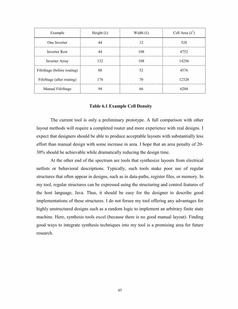
Example Height (λ) Width (λ) Cell Area (λ2)
One Inverter 44 12 528
Inverter Row 44 108 4752
Inverter Array 132 108 14256
FifoStage (before routing) 88 52 4576
FifoStage (after routing) 176 70 12320
Manual FifoStage 94 66 6204
The current tool is
layout methods will require
expect that designers shoul
effort than manual design
30% should be achievable
At the other end of
netlists or behavioral des
structures that often appear
my tool, regular structures
the host language, Java.
implementations of these s
highly unstructured design
machine. Here, synthesis t
good ways to integrate syn
research.
Table 6.1 Example Cell Density45
only a preliminary prototype. A full comparison with other
a completed router and more experience with real designs. I
d be able to produce acceptable layouts with substantially less
with some increase in area. I hope that an area penalty of 20-
while dramatically reducing the design time.
the spectrum are tools that synthesize layouts from electrical
criptions. Typically, such tools make poor use of regular
in designs, such as in data-paths, register files, or memory. In
can be expressed using the structuring and control features of
Thus, it should be easy for the designer to describe good
tructures. I do not forsee my tool offering any advantages for
s such as a random logic to implement an arbitrary finite state
ools excel (because there is no good manual layout). Finding
thesis techniques into my tool is a promising area for future

46
CHAPTER 7 CONCLUSIONS AND FUTURE WORK
As covered in this thesis, automatic circuit layout generation involves the deployment
and integration of many design automation techniques to produce high quality layouts
from an initial transistor level or low level description. This thesis identifies
opportunities for circuit optimization across design phases, and describes a fully
automatic layout generation tool implemented in Java. The system is flexible enough to
handle many process technologies and a wide variety of layout styles. The tool is fully
automatic and provides several options to the user to customize the layout. The tool
considers performance and generates dense, design rule correct layouts. Experimental
results indicate that the area of generated layouts is competitive with manually designed
cells for the circuits tried. Run times plus the times needed to write the description of the
circuit are dramatically shorter than a human would require to manually create similar
layouts, allowing a designer to try more topological variations to obtain an optimal
design. Moreover, this tool allows us to target new technologies as they emerge, since
only changes in the input technology file are needed.
As most other systems developed in the area of automatic layout generation, this
tool also focuses on specific, fundamental problems related to transistor placement,
routing, and compaction, and is described mainly to demonstrate its specific innovations.
The more general direction for future work, and the promise of greater impact, is to look
back on many ignored but practical problems essential to fully automatic layout
generation, such as transistor folding6 to meet cell height requirements and minimum
width, well and substrate tie insertion to meet tie coverage requirements in an area
efficient way, input/output port placement on a routing grid for compatibility with place
and route tools, circuit performance issues, automatic jog insertion to minimize area and
6 Transistor folding is the process of splitting a transistor into multiple transistors of smaller widths connected in parallel. Intelligent transistor folding is crucial to automatic layout generation because it automatically generates area-optimized layouts.

47
wire length to achieve hand-packed density, and more flexible architectures, such as
transistor stacking. Considerable further research needs to be done.
The current tool is definitely a prototype, and in many ways, it is an experiment
to demostrate that we are able to generate layouts using very simple techniques. In
particular, I provide the API that makes it easy for the designer to describe the design
topology. The designer uses the structuring mechanisms of Object-Oriented
programming to construct complicated designs using the simple API. Tedious details of
physical placement and routing are handled by my tool.
Future research along this line should address how more issues of design and
optimization can be incorporated into the simple framework. First, many optimization
problems for layout synthesis can be expressed or approximated by linear or convex
programming problems. These include, for example, retiming, transistor sizing and
performance-driven routing. As many of these problems are NP-complete, formulations
based on linear or convex programming are necessarily approximations. Our hope is that
these convex formulations will lead to predictable results allowing the designer to find
good layouts.
On the other hand, unlike most of the efforts made in the layout synthesis that are
dedicated to specific improvements, our tool aims to provide a general high-level
solution and free the designer from the need to get familiar with quite a few different
optimization tools. We hope that in this way our tool will incorporate all the different
optimization tools into a general framework, and by Object-Oriented design have an
object view of the circuit and apply the structuring mechanisms. More efforts still need
to be made to incorporate different optimization features into our prototype.

48
BIBLIOGRAPHY
[Chen 89] C. C. Chen and S.-L. Chow. “The Layout Synthesizer: An
Automatic Netlist-to-layout System”. In the 26th ACM/IEEE
Design Automation Conference, pages 232-238, 1989.
[Choudhury 93] U. Choudhury and A. Sangiovanni-Vincentelli. “Automatic
Generation of Parasitic Constraints for Performance-constrained
Physical Design of Analog Circuits”. IEEE Transactions on
Coputer-Aided Design, Vol. 12, pages 208-224, February 1993.
[Dao 93] Joseph Dao, Nobu Matsumoto, Tsuneo Hamai, Chusei Ogawa,
and Shojiro Mori. “A Compaction Method for Full Chip VLSI
Layouts”. In the 30th ACM/IEEE Design Automation Conference,
1993.
[Domic 89] A. Domic, S. Levitin, N. Phillips, C. Thai, T. Shiple, D. Bhavsar,
and C. Bissel. “CLEO: A CMOS Layout Generator”. Proceedings
of ICCAD-89, pages 340-343, 1989.
[Draney 89] M. Draney, R. “Method and Apparatus for Recording and
Rearranging Representations of Objects in A Coordinate System”.
U.S. patent #4829446, 1989.
[Duh 95] J. Duh, T. G. Matheson, and E. Hepler. “Efficiently Embedding
Expertise in High-density Process-portable, Standard Cell
Generators”. Proceedings of IEEE Custom Integrated Circuit
Conference, pages 497-500, 1995.
[Dunlop 80] A. E. Dunlop. “SLIM: The Translation of Symbolic Layout into
Mask Data”. Proceedings of the 17th ACM/IEEE Design
Automation Conference, pages 595-602, 1980.
[Duvall 99] Steve Duvall. “Optimization Problems in Integrated Circuit
Design”. In a seminar held at UBC Commerce in 1999.

49
[Gamma 95] Erich Gamma, Richard Helm, Ralph Johnson, and John Vlissides.
Design Patterns: Elements of Reusable Object-Oriented Software.
Addison-Wesley, 1995.
[Gupta 96] A. Gupta, S. The and J. P. Hayes. “XPRESS: A Cell Layout
Generator with Integrated Transistor Folding”. Proceedings of
European Design and Test Conference, March 1996, pages 393-
400.
[Gupta 97] Avaneendra Gupta and John P. Hayes. “CLIP: An Optimizing
Layout Generator for Two-Dimensional CMOS Cells”. In the 34th
ACM/IEEE Design Automation Conference, 1997.
[Guruswamy 97] Mohan Guruswamy, Robert L. Maziasz, Daniel Dulitz, Srilata
Raman, Venkat Chiluvuri, Andrea Fernandez, and Larry G. Jones.
“CELLERITY: A Fully Automatic Layout Synthesis System for
Standard Cell Libraries”. In the 34th ACM/IEEE Design
Automation Conference, 1997.
[Hill 85] Dwight D. Hill. “Sc2: A Hybrid Automatic Layout System”.
Proceedings of ICCAD-85, pages 172-174, 1985.
[Lakos 97] John Lakos. “Technology Retargeting for IC Layout”. In the 34th
ACM/IEEE Design Automation Conference, 1997.
[Lea 94] Doug Lea. “Christopher Alexander: An Introduction for Object-
Oriented Designers”. In Software Engineering Notes, 1994.
[Lefebvre 97] Martin Lefebvre, David Marple, and Carl Sechen. “The Future of
Custom Cell Generation in Physical Synthesis”. In the 34th
ACM/IEEE Design Automation Conference, 1997.
[Lotvin 84] M. Lotvin, B. Juran, and R. Goldi. “AMOEBA: A Symbolic VLSI
Layout System”. Proceedings of the 21st ACM/IEEE Design
Automation Conference, pages 294-300, 1984.
[Krambeck 82] R. H. Krambeck, C. M. Lee, and H. S. Law. “High-speed
Compact Circuits with CMOS”. IEEE Journal of Solid-State
Circuits, Vol. 17, pages 614-619, June 1982.

50
[Marple 88] D. Marple, M. Smulders, and H. Hegen. “An Efficient Compactor
for 45º Layout”. Proceedings of the 25th ACM/IEEE Design
Automation Conference, pages 396-402, 1988.
[Matheson 85] T. G. Matheson, C. Christensen, and M. R. Buric. “A Software
Environment for Buliding Core Microprocessor Compilers”.
Proceedings of ICCD, pages 221-224, 1985.
[Mathias 98] Herve Mathias, Josette Berger-Toussan, Gilles Jacquemod,
Frederic Gaffiot, and Michel Le Helley. “FLAG: A Flexible
Layout Generator for Analog MOS Transistors”. IEEE Journal of
Solid-State Circuits, Vol. 33, No. 6, June 1998.
[Mogaki 91] M. Mogaki, N. Kato, N. Shimada, and Y. Yamada. “A Layout
Improvement Method Based on Constraint Propagation for
Analog LSI’s”. In the 28th ACM/IEEE Design Automation
Conference, pages 510-513, 1991.
[Ong 89] C.-L. Ong, J.-T. Li, and C.-Y. Lo. “GENAC: An Automatic Cell
Synthesis Tool”. In the 26th ACM/IEEE Design Automation
Conference, pages 239-244, 1989.
[Ousterhout 84] J. Ousterhout, G. Hamachi, R. Mayo, W. Scott, and G. Taylor.
“Magic: A VLSI Layout System”. Proceedings of the 21st Design
Automation Conference, pages 152-159, 1984.
[Park 00] Soondal Park. “LPABO ver 5.72 User Manual (2000.5.2)”.
http://orlab.snu.ac.kr/pub/software/lpabo/lpabo572.wp
[Poirier 89] C. J. Poirier. “Excellerator: Custom CMOS Leaf Cell Layout
Generator”. IEEE Transactions on CAD, Vol. 8, No. 7, July 1989,
pages 744-755.
[Rekhi 95] Sanjay Rekhi, J. Donald Trotter, and Daniel H. Linder.
“Automatic Layout Synthesis of Leaf Cells”. In the 32nd
ACM/IEEE Design Automation Conference, 1995.
[Sadakane 95] T. Sadakane, H. Nakao, and M. Terai. “A New Hierarchical
Algorithm for Transistor Placement in CMOS Macro Cell
Design”. Proceedings of CICC-95, pages 461-464, 1995.

51
[Serdar 99] Tatjana Serdar and Carl Sechen. “AKORD: Transistor Level and
Mixed Transistor/Gate Level Placement Tool for Digital Data
Paths”. In International Conference on CAD, November 1999.
[Tani 91] K. Tani, K. Izumi, M. Kashimura, T. Matsuda and T. Fujii. “Two-
dimensional Layout Synthesis for Large-scale CMOS Circuits”.
Proceedings of ICCAD-91, pages 490-493, 1991.
[Weste 93] Neil H. E. Weste and Kamran Eshragian. Principles of CMOS
VLSI Design. 2nd Edition. Addison-Wesley, 1993.
[Wimer 87] S.Wimer, R. Pinter, and J. Feldman. “Optimal Chaining of CMOS
Transistors in A Functional Cell”. IEEE Transactions on CAD,
Vol. 6, No. 5, September 1987, pages 795-801.

52
APPENDIX A LAYOUT GENERATION TOOL SOURCE
This appendix contains full source code for my layout generation tool. The Circuit
package is presented first, followed by the Constraints package and the Magic package.
Table A.1 lists the index of all the source files.
package Circuit
abstract class Circuit 55
class CircuitInvalidException 56
class CircuitRow 57
class DefaultSignal 57
class GeomCircuit 58
class GeomRow 60
class GeomRowProto 61
class Ground 64
class Layer 65
class NRow 65
class NTransistor 67
class Node 67
class PRow 68
class PTransistor 69
class Power 70
class Rectangle 71
class RoutingRow 71
(Table A.1, continued on next page)

53
(continuation of Table A.1)
abstract class Row 72
class RowNTran 75
class RowPTran 76
abstract class RowTran 77
class Scmos 77
interface Signal 78
abstract class Trow 79
class Technology 79
class Terminal 80
class Transistor 81
package Constraints
class Coefficient 82
class Constraint 82
class ConstraintEdge 83
class ConstraintGraph 83
abstract class ConstraintSet 86
class Equality 88
class Expr 89
class Inequality 89
interface LPfactory 90
interface LinearProgram 90
class Lpabo 91
interface OPfactory 93
class Opt 94
class RowVector 96
(Table A.1, continued on next page)

54
(continuation of Table A.1)
class Valuation 96
class Variable 97
package Magic
class MagicOutput 99
class MagicWriter 100
Table A.1 Index of Layout Generation Tool Source

55

56

57

58

59

60

61

62

63

64

65

66

67

68

69

70

71

72

73

74

75

76

77

78

79

80

81

82

83

84

85

86

87

88

89

90

91

92

93

94

95

96

97

98

99

100

101
APPENDIX B LAYOUT GENERATION EXAMPLE SOURCE
This appendix includes the four example source tested in Chapter 6. In a similar way, the
designer can write a description of a target circuit using the API provided in Appendix
A. Table B.1 lists the index of all the example files.
class FifoStage 102
class Inv 103
class Invs 104
class newInv 105
Table B.1 Index of Layout Generation Example Source

102

103

104

105
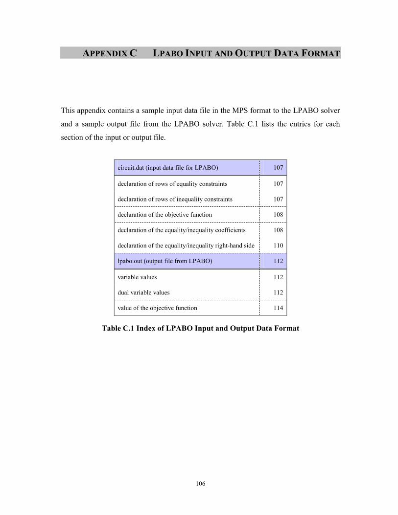
106
APPENDIX C LPABO INPUT AND OUTPUT DATA FORMAT
This appendix contains a sample input data file in the MPS format to the LPABO solver
and a sample output file from the LPABO solver. Table C.1 lists the entries for each
section of the input or output file.
circuit.dat (input data file for LPABO) 107
declaration of rows of equality constraints 107
declaration of rows of inequality constraints 107
declaration of the objective function 108
declaration of the equality/inequality coefficients 108
declaration of the equality/inequality right-hand side 110
lpabo.out (output file from LPABO) 112
variable values 112
dual variable values 112
value of the objective function 114
Table C.1 Index of LPABO Input and Output Data Format

107

108

109

110

111

112

113

114

115
APPENDIX D MAGIC FILE FORMAT
This appendix includes a sample file in the Magic format, the generated
“FifoStage.mag”.

116

117