An Array-Based Circuit for Characterizing Latent Plasma ...
21
An Array-Based Circuit for Characterizing Latent Plasma-Induced Damage Won Ho Choi, Pulkit Jain and Chris H. Kim University of Minnesota, Minneapolis, MN [email protected] www.umn.edu/~chriskim/
Transcript of An Array-Based Circuit for Characterizing Latent Plasma ...

An Array-Based Circuit for Characterizing Latent
Plasma-Induced DamageWon Ho Choi, Pulkit Jain
and Chris H. Kim
University of Minnesota, Minneapolis, MN
[email protected]/~chriskim/

2/21
Purpose
• Design a dedicated on-chip array-based
circuit for efficiently characterizing latent
plasma-induced damage.
• Collect massive time-to-breakdown data
from devices with various antenna
topologies in a short test time.

3/21
Outline
• Plasma-Induced Damage (PID)
• Array-Based PID Characterization Circuit
• Antenna Design
• Stress Experiment Results
• Conclusions

4/21
Plasma-Induced Damage (PID)
• Plasma charge generated during the fabrication process leads to damage in the gate dielectric manifesting as latent BTI and TDDB reliability issues.
• The contiguous metal structure referred to as “antenna”
Z. Wang, et al., ICICDT 2005

5/21
Characterizing “Latent” PID: BTI vs. TDDB
“Bias Temperature Instability”“Time Dependent Dielectric Breakdown”
• BTI & TDDB methods have to be considered together in order to fully understand the impact of latent PID on device and circuit reliability

6/21
TDDB Aggravated by PID

7/21
Circuit Impact and Mitigation Techniques
P. H. Chen, IEEE Circuits & Devices Magazine 2004
• Mitigation techniques incur speed, power, cost, and time-to-market overhead
• PID impact on circuits need to be accurately assessed

8/21
Device probingWafer probe system
Array-Based system
Device Probing
Array-based
Meas. time
1
Wafer area
1
*1/n2 *1/n2
Measurement
Off-chip tester
On-chip current to digital
Scalability
No
Yes
*nxn array, parallel stress
PID Characterization MethodDevice Probing vs. Array-Based System
P. Jain, et al., ESSDERC 2012

9/21
Proposed PID Characterization Array
• 12x24 stress cells array allows parallel stress/serial measurement capability
• Three types of antenna implemented: plate-type antenna, fork-type antenna, no antenna
10/21
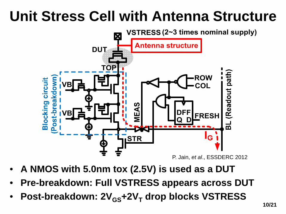
Unit Stress Cell with Antenna Structure
• A NMOS with 5.0nm tox (2.5V) is used as a DUT• Pre-breakdown: Full VSTRESS appears across DUT• Post-breakdown: 2VGS+2VT drop blocks VSTRESS
P. Jain, et al., ESSDERC 2012

11/21
On-Chip Current-to-Digital Converter
• Fast evaluation of progressive TDDB behavior in the DUT cell
• IG of each DUT measured sequentially and converted to a digital count and read off-chip
BL

12/21
PID during Plasma Etching / Ashing
• Etching: plasma charging current is proportional to metal perimeter area
• Ashing : plasma charging current is proportional to metal top surface area
H. Shin, et al., IRPS 1992

13/21
Plate and Fork Type Antenna
• Fork type antenna consists of numerous metal fingers and hence occupies a larger silicon area than the plate type antenna for the same antenna ratio (AR)

14/21
Metal Layer Usage and Antenna Ratio
• Each antenna consists of 5 metal layers (M2-M6)• AR values of 10k and 20k were implemented

15/21
Layout View of Three Stress Cells
(a) Upper layers[M5-M6]
(b) Lower layers[M2-M4]

16/21
Cross-sectional View of Antenna Structure
• A small M7 jumper line was used to maximize the PID damage occurring while forming layers M2-M6
Area(M7)AR(Plate, Fork)Area(Gate) (12 24)
Area(M7)AR(No antenna)
Area(M2-M6)Area(Gat
Area(Gate) (12 24)
e)≈ +
× ×
≈× ×
∑

17/21
Measured Breakdown Data @ 6.5V
• The cumulative time-to-breakdown curve shifts to the left for DUT array with larger antennas
• DUT array with plate antenna shows a consistently shorter lifetime compared to its fork type counterpart– Lifetime degradation of the fork (or plate) antenna with 10k AR:
7.7% (or 10.2%) for a 6.5V stress voltage
75
80
85
90
95
100
6.5
No antennaFork (10k AR)Plate (10k AR)Fork (20k AR)Plate (20k AR)
VSTRESS (V)
MTT
F (6
3%, n
orm
aliz
ed)

18/21
Measured Breakdown Data @ 6.7V
75
80
85
90
95
100
6.7
No antennaFork (10k AR)Plate (10k AR)Fork (20k AR)Plate (20k AR)
VSTRESS (V)M
TTF
(63%
, nor
mal
ized
)VSTRESS (V)
MTT
F (6
3%, n
orm
aliz
ed)
• Similar trends for a higher stress voltage of 6.7V• Larger antenna shows worse PID • Plate type antenna has worse PID than fork type

19/21
Chip-to-Chip Variation
• Time-to-breakdown trend consistent across different chips
• Measured data suggests that PID during the etching is relatively small compared to that during the ashing

20/21
65nm Die Photo and Chip Features

21/21
Conclusions• Array-based PID characterization circuit with various
antenna structures fabricated in a 65nm process
– Reduces the stress time and silicon area by a factorproportional to the number of DUTs to be tested
– An effective research tool for understanding PID effects
• Time-to-breakdown curve shifts to the left for DUTarray with larger antennas
• DUT with plate antenna has a consistently shorterlifetime compared to its fork type counterpart
– Suggests that PID during the etching step is relatively small compared to that during the ashing step