An Analysis of DMA Interference Using Synthetic Load from ... · An Analysis of DMA Interference...
50
An Analysis of DMA Interference Using Synthetic Load from an NVMe Device Bachelorarbeit von Lukas Werling an der Fakultät für Informatik Erstgutachter: Prof. Dr. Frank Bellosa Zweitgutachter: Prof. Dr. Wolfgang Karl Betreuender Mitarbeiter: Dipl.-Inform. Marius Hillenbrand Bearbeitungszeit: 19. Mai 2015 – 18. September 2015 KIT – Universität des Landes Baden-Württemberg und nationales Forschungszentrum in der Helmholtz-Gemeinschaft www.kit.edu
-
Upload
hoanghuong -
Category
Documents
-
view
220 -
download
0
Transcript of An Analysis of DMA Interference Using Synthetic Load from ... · An Analysis of DMA Interference...

An Analysis of DMA InterferenceUsing Synthetic Load from an NVMe
Device
Bachelorarbeitvon
Lukas Werlingan der Fakultät für Informatik
Erstgutachter: Prof. Dr. Frank BellosaZweitgutachter: Prof. Dr. Wolfgang KarlBetreuender Mitarbeiter: Dipl.-Inform. Marius Hillenbrand
Bearbeitungszeit: 19. Mai 2015 – 18. September 2015
KIT – Universität des Landes Baden-Württemberg und nationales Forschungszentrum in der Helmholtz-Gemeinschaft www.kit.edu


Ich erkläre hiermit, dass ich die vorliegende Arbeit selbständig verfasst undkeine anderen als die angegebenen Quellen und Hilfsmittel verwendet habe.
Karlsruhe, den 18. September 2015

iv

Abstract
With the general availability of PCI Express 3.0 slots in both consumer andserver hardware today, more and more devices making use of the fast transferspeed are being released. These devices read and write directly into the mainmemory using Direct Memory Access (DMA).
Other works [2] have already determined that memory-intensive applica-tions running in parallel on a multi-core platform may slow each other downdue to the memory controller reordering requests. In this work, we analyzeinterference of high-bandwidth DMA operations with applications runningin parallel on the CPU. To generate DMA load, we design and implement aload generator based on NVMe solid-state drives.
Our experiments show that high-bandwidth DMA transfers indeed havean in�uence on memory-intensive applications. Additionally, we characterizebandwidth and command rate of our NVMe device and analyze last-levelcache usage with performance counters.
v

vi ABSTRACT

Contents
Abstract v
1 Introduction 3
2 Background 5
2.1 DMA . . . . . . . . . . . . . . . . . . . . . . . . . . . . . . . . 52.2 NVMe . . . . . . . . . . . . . . . . . . . . . . . . . . . . . . . 62.3 Performance Counter Monitoring . . . . . . . . . . . . . . . . 72.4 PARSEC . . . . . . . . . . . . . . . . . . . . . . . . . . . . . . 92.5 Silo . . . . . . . . . . . . . . . . . . . . . . . . . . . . . . . . . 10
3 Design 11
3.1 DMA Load Generator . . . . . . . . . . . . . . . . . . . . . . 113.1.1 Memory Access Patterns . . . . . . . . . . . . . . . . . 123.1.2 Con�guration Options . . . . . . . . . . . . . . . . . . 13
3.2 Performance Counter Analysis . . . . . . . . . . . . . . . . . . 13
4 Implementation 15
4.1 DMA Load Generation . . . . . . . . . . . . . . . . . . . . . . 154.1.1 Patterns and Parallelization . . . . . . . . . . . . . . . 164.1.2 Bandwidth and Command Limiting . . . . . . . . . . . 164.1.3 Caching . . . . . . . . . . . . . . . . . . . . . . . . . . 17
4.2 NVMe Linux Driver Customization . . . . . . . . . . . . . . . 174.3 Performance Counter Analysis . . . . . . . . . . . . . . . . . . 17
5 Evaluation 19
5.1 Test Systems . . . . . . . . . . . . . . . . . . . . . . . . . . . 195.2 DMA Load . . . . . . . . . . . . . . . . . . . . . . . . . . . . 205.3 Syscall Batching . . . . . . . . . . . . . . . . . . . . . . . . . . 225.4 Performance Counter Monitoring . . . . . . . . . . . . . . . . 23
5.4.1 NVMe Command Counts . . . . . . . . . . . . . . . . . 24
1
2 CONTENTS
5.4.2 Bandwidth . . . . . . . . . . . . . . . . . . . . . . . . . 255.4.3 Caching . . . . . . . . . . . . . . . . . . . . . . . . . . 27
5.5 DMA Interference . . . . . . . . . . . . . . . . . . . . . . . . . 285.5.1 PARSEC . . . . . . . . . . . . . . . . . . . . . . . . . 305.5.2 In-memory Databases . . . . . . . . . . . . . . . . . . . 32
6 Conclusion 37
6.1 Future Work . . . . . . . . . . . . . . . . . . . . . . . . . . . . 38
A Full PARSEC Results 39
Bibliography 43

Chapter 1
Introduction
All applications running on modern computers are accessing the main mem-ory more or less extensively. With multicore CPUs, multiple programs willaccess the memory at the same time. Due to the organization of DRAM,some requests can be ful�lled faster than others. Making use of this fact,the memory controller reorders memory requests, improving overall mem-ory throughput. However, this may reduce performance of a process whosememory requests are ful�lled less often.
This e�ect is similar to issues with preemptive CPU scheduling: A �fair�usage share of CPU time for every process is often desired. Priorities canusually be given to processes by di�erent criteria, for example to make surethat an interactive application runs more often than a background process.
Managing memory bandwidth on the application level is already possiblewith MemGuard [2]. This method relies on an estimate of the worst-casememory bandwidth available, distributing the bandwidth to processes basedon hardware performance counters built into newer CPUs. These countersmeasure the bandwidth each CPU core is using.
The maximum memory bandwidths of current CPUs vary a lot. Con-sumer CPUs usually have a maximum bandwidth of about 25 GB/s [4],while upcoming high-end server CPUs support up to 100 GB/s [9]. Our twotest systems used for this thesis (see Section 5.1) support 21 GB/s (SandyBridge) and 59 GB/s (Haswell). However, the actual achievable bandwidthdepends a lot on the memory access pattern. For example, randomly ac-cessing small chunks of memory has less throughput than a long sequentialread.
The MemGuard authors focused on the memory usage of applicationsand did not take another important contender to memory bandwidth intoaccount: Modern I/O devices transfer data to the CPU by writing directlyto main memory (Direct Memory Access, DMA).
3

4 CHAPTER 1. INTRODUCTION
For their system, the MemGuard authors estimated a worst-case band-width of only 1.2 GB/s, which is roughly equal to the rate of 10 GigabitEthernet. Consequently, their algorithm may not be able to distribute mem-ory bandwidth properly while a DMA transfer from the network card is inprogress.
With devices such as solid-state drives (SSD) and Ethernet controllersgetting faster, DMA transfers can now take a signi�cant proportion of theavailable memory bandwidth shared with the CPU.
Newer SSD models based on NVMe [12] are promising data transferswith up to 3.2 GB/s [15]. On a desktop computer with a quad-core CPUand a memory bandwidth of 25.6 GB/s, each core usually has 6.4 GB/savailable. Thus, a full-speed DMA transfer would cut a single core's memorybandwidth in half. As real-world limits are likely smaller depending on theaccess patterns, the actual in�uence may be even larger.
The main contribution of this work is a �exible and extendible DMAload generator based on NVMe. In the following Chapter 2, we providebackground information on technologies we used, such as DMA and NVMe.In Chapter 3, we discuss the design, and in Chapter 4 the implementationof our load generator. Chapter 5 contains our evaluation: We analyze themaximum bandwidth of our SSD, evaluate the use of performance countersto characterize NVMe tra�c, and test interference with several benchmarkprograms. Finally, we summarize our results in Chapter 6, presenting aconclusion and proposing future work.

Chapter 2
Background
This chapter provides background information on technologies and tools usedin this work: We �rst explain some details on DMA (Section 2.1). In Section2.2, we then give an overview on the NVMe interface. Finally, we presenttools we used for the evaluation: Intel's Performance Counter Monitor (Sec-tion 2.3), the PARSEC benchmark suite (Section 2.4) and the Silo in-memorydatabase (Section 2.5).
2.1 DMA
Direct memory access (DMA) allows external devices to access the mainmemory independently from the CPU. Usually, the CPU requests a transferfrom an external device. The device then can transfer its data directly fromor to the main memory. During the transfer, the CPU is not blocked andcan do other work. When the transfer �nishes, the device noti�es the CPUusing an interrupt.
During the transfer, requests from both the CPU and the external devicemay reach the memory controller. Thus, memory accesses by the CPU maybe slowed down. We analyze this interference in Section 5.5.
Another issue with DMA is cache coherency: In contrast to the CPU withits cache hierarchy, the external devices access the main memory directly.Consequently, devices may read stale data, which the cache has not writtenback yet, or the caches may serve the CPU data that changed in memoryin the meantime. To solve these issues, the cache needs to be invalidated aspart of the DMA operations, slowing down reads and writes by the CPU andadding load to the memory controller.
Intel's DDIO technology [3] aims to improve this situation. It makes thelast-level cache (LLC) the primary target of DMA operations. This solves
5

6 CHAPTER 2. BACKGROUND
the cache coherency issue, as mechanisms for coherency with the higher-level caches, which are speci�c to the individual CPU cores, are already inplace for multicore systems. Memory controller contention is also improved:Especially for frequent, small transfers such as those from network cards, themain memory is not involved in the transfers at all, speeding up processingconsiderably.
Having DMA writing to the LLC directly may reduce the amount ofcache available to applications. However, Intel also greatly increased thetotal amount of last-level cache, making up to 20 MB cache possible [5].Thus, this LLC usage is unlikely to slow down applications compared toCPUs without DDIO.
Our Sandy Bridge test system does not support the DDIO technology,but the Haswell system does (see Section 5.1 for an overview of our systems).In Section 5.4.3, we analyze LLC usage on the Haswell system.
2.2 NVMe
Non-Volatile Memory Express (NVMe) [12] is a communication interface de-signed for solid-state drives (SSD) connected via PCI Express. It allowsfor higher transfer rates with more parallelism compared to the older SA-TA/AHCI interface, which was primarily designed for hard disk drives. TheNVMe speci�cation de�nes a command set consisting of Admin and IO com-mands.
The Admin commands are primarily used by the NVMe driver to set updrives for data transfers. They allow querying drive-speci�c information aswell as setting options, such as power management.
The IO commands are used for the actual data transfers. The NVMespeci�cation de�nes three mandatory commands: Read, Write, and Flush.The Read and Write commands take a location in main memory as well asa logical block address and transfer data to or from the SSD. The Flushcommand instructs the SSD to write any changes from previous commandsfrom its caches to non-volatile media.
All communication with the SSD happens with submission and comple-tion queues located in main memory. The driver submits its commands to asubmission queue. The SSD accesses commands from this queue via DMA.After processing a command, the SSD submits a completion entry to the com-pletion queue, again with DMA. The driver usually waits for the completionentry, allowing other threads to run in the meantime.
Each NVMe controller has a single Admin Submission Queue and anAdmin Completion Queue. IO commands are managed in separate IO Sub-
2.3. PERFORMANCE COUNTER MONITORING 7
mission and Completion queues. With Admin commands, the NVMe drivercan create multiple of them on demand.
Multiple queues improve performance as they allow the SSD to processrequests in parallel. The NVMe Linux driver usually creates one IO Submis-sion and one IO Completion Queue per CPU core.
IO operations work analogous to the Admin operations: The driver sub-mits an IO command to one of its IO Submission Queues. The SSD thenperforms the data transfer and noti�es completion to the driver by postinga completion entry to one of the IO Completion Queues. So in addition tothe user data, an NVMe command of 64 B is transferred to the SSD and acompletion entry of 16 B is transmitted from the SSD per operation.
Each IO operation can transfer multiple logical SSD blocks. The max-imum number of blocks is speci�c to the SSD; our model (see Section 5.1)allows transferring 32 blocks of 4096 B per command.
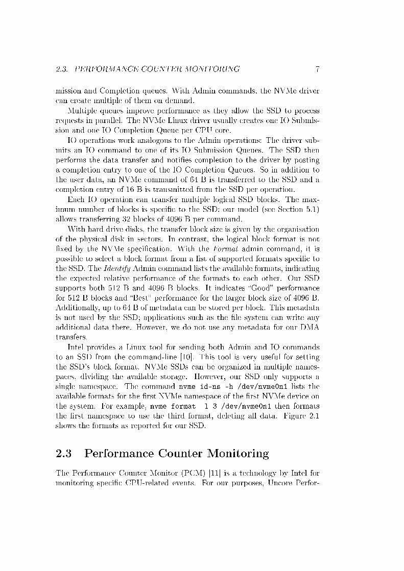
With hard drive disks, the transfer block size is given by the organisationof the physical disk in sectors. In contrast, the logical block format is not�xed by the NVMe speci�cation. With the Format admin command, it ispossible to select a block format from a list of supported formats speci�c tothe SSD. The Identify Admin command lists the available formats, indicatingthe expected relative performance of the formats to each other. Our SSDsupports both 512 B and 4096 B blocks. It indicates �Good� performancefor 512 B blocks and �Best� performance for the larger block size of 4096 B.Additionally, up to 64 B of metadata can be stored per block. This metadatais not used by the SSD; applications such as the �le system can write anyadditional data there. However, we do not use any metadata for our DMAtransfers.
Intel provides a Linux tool for sending both Admin and IO commandsto an SSD from the command-line [10]. This tool is very useful for settingthe SSD's block format. NVMe SSDs can be organized in multiple names-paces, dividing the available storage. However, our SSD only supports asingle namespace. The command nvme id-ns -h /dev/nvme0n1 lists theavailable formats for the �rst NVMe namespace of the �rst NVMe device onthe system. For example, nvme format -l 3 /dev/nvme0n1 then formatsthe �rst namespace to use the third format, deleting all data. Figure 2.1shows the formats as reported for our SSD.
2.3 Performance Counter Monitoring
The Performance Counter Monitor (PCM) [11] is a technology by Intel formonitoring speci�c CPU-related events. For our purposes, Uncore Perfor-

8 CHAPTER 2. BACKGROUND
# nvme id -ns -h /dev/nvme0n1
[...]
LBA Format 0 : Metadata Size: 0 bytes - Data Size: 512 bytes
- Relative Performance: 0x2 Good
LBA Format 1 : Metadata Size: 8 bytes - Data Size: 512 bytes
- Relative Performance: 0x2 Good
LBA Format 2 : Metadata Size: 16 bytes - Data Size: 512 bytes
- Relative Performance: 0x2 Good
LBA Format 3 : Metadata Size: 0 bytes - Data Size: 4096 bytes
- Relative Performance: 0 Best (in use)
LBA Format 4 : Metadata Size: 8 bytes - Data Size: 4096 bytes
- Relative Performance: 0 Best
LBA Format 5 : Metadata Size: 64 bytes - Data Size: 4096 bytes
- Relative Performance: 0 Best
LBA Format 6 : Metadata Size: 128 bytes - Data Size: 4096 bytes
- Relative Performance: 0 Best
Figure 2.1: Abridged output of the nvme id-ns command for our SSD.
mance Monitoring counters located at the last-level cache (LLC) are inter-esting. These counters count read and write accesses to the LLC. As withDDIO (see Section 2.1) all main memory accesses by the CPU and by ex-ternal devices need to pass the LLC, we can use these counters to estimatethe memory bandwidth used by applications and devices. In contrast to themore common CPU counters, the Uncore counters are only available for someCPUs [7].
A performance counter is essentially a simple integer variable. It can betuned to a speci�c event.1 Whenever this event occurs in a cache line, thevariable is incremented by one. The events are further divided in cache hitsand cache misses. In case of a cache miss, the LLC fetches the cache linefrom main memory, recording a cache hit afterwards (see Section 5.4.3). TheCPU can read the counter's current value at any time. However, a countermay only monitor a single event at a time. Consequently, we either haveto switch the counter rapidly between multiple events or run the measuredprogram multiple times with di�erent events.
As the events are triggered per cache line, which are 64 B, a single eventusually means a read or write of 64 B of data. However, some events arealso triggered for partial reads or writes, occurring when data is unaligned orwhen the access size is smaller than 64 B. Therefore, a single event indicates
1In fact, we are only looking at a single event in the sense of the Uncore documentation.
This event is �ltered by Opcode and Thread-ID. When we say �event� here, we are actually
referring to a speci�c combination of Opcode and Thread-ID.
2.4. PARSEC 9
a data transfer of 64 B or less.On our Haswell platform (see Section 5.1), the following events are avail-
able:
PCIeRdCur �PCIe read current transfer� � This event is triggered when aPCIe device reads from a cache line. It does not distinguish betweenfull and partial reads, so the reported number is likely higher thanestimates from transfer size.
RFO �PCIe partial write� � This event is shared with the CPU, but can be�ltered for activity from PCIe. In this context, it counts partial writes(i.e., writes smaller than 64 B) to cache lines.
ItoM �PCIe write full cache line� � Just like RFO, this event is shared withthe CPU and can be �ltered. It counts full writes of 64 B to cache lines.The sum of RFO and ItoM corresponds to what PCIeRdCur reportsfor reading.
CRd �Demand Code Read�
DRd �Demand Data Read� � CRd and DRd are read events occurring whenthe CPU reads code or data from the last-level cache. These events arenot directly related to PCIe tra�c.
PRd �MMIO read�
WiL �MMIO write� � PRd and WiL events are recorded when the CPU doesmemory-mapped IO (MMIO) read or write. While this mechanism isused for communication with devices, it does not convey informationabout NVMe activity where the SSD device communicates using queuesin memory.
2.4 PARSEC
PARSEC [1] is a benchmark suite with a focus on multithreaded applica-tions. It consists of 13 workloads, of which we tested all except facesim andfluidanimate (see Section 5.5.1).
As we are using the benchmark programs to analyze interference of mem-ory accesses, we are especially interested in workloads that have high levelsof main memory usage. Figure 4.7 of the PARSEC overview paper [1] givesa breakdown of o�-chip tra�c (i.e., memory accesses that cannot be satis�edby a cache) of the PARSEC workloads. Note that the raytrace workload ismissing from the graph.
10 CHAPTER 2. BACKGROUND
The top workloads regarding memory usage in the graph are streamclus-ter, canneal, and facesim. The streamcluster and canneal workloads,along with raytrace, are also the workloads that showed interference in ourevaluation in Section 5.5.1.
2.5 Silo
Silo [18] is an in-memory database designed to achieve high performance onmulticore systems. Its authors demonstrate that Silo scales almost linearlyto multiple cores.
An in-memory database is well suited to analyze DMA interference asits core objective is to store and retrieve large amounts of data from mainmemory as quickly as possible.

Chapter 3
Design
This chapter describes the design of a DMA load generator based on NVMe.The load generator needs to satisfy several goals: We want it to supportdi�erent memory access patterns (Section 3.1.1) and it needs to supportcon�guration options such as the number of workers used (Section 3.1.2).Additionally, it should support using performance counters to evaluate itsperformance (Section 3.2).
3.1 DMA Load Generator
In this section, we describe our DMA load generator.
The standard way of transferring data from and to an SSD works byreading and writing �les on a �le system. While this works �ne for generatingsome load, there is little control over the exact size and memory location ofthe transfers as the operating system provides a cache between the deviceand client applications. Additionally, having as little overhead as possibleis important as the load generation runs in parallel to the benchmarkingapplications.
Therefore, we decided to bypass the operating system and issue NVMecommands to the SSD directly. The core of the NVMe command set are thethree commands read, write, and flush. The read and write commandstransfer data from or to the SSD. The flush command instructs the SSDto persist anything written in previous commands and does not transfer anydata.
In addition to these I/O commands, NVMe speci�es an admin commandset whose commands are used to identify features speci�c to the SSD and tocon�gure the SSD.
In order to generate DMA load, we allocate a memory bu�er of �xed size
11

12 CHAPTER 3. DESIGN
in our load generator, which is then used directly as target of the NVMecommands. We can then transfer data using read or write commands.These commands share a memory layout and are both given a block rangeon the SSD identi�ed by a logical block address and count, and an addressin memory. Switching between reading and writing thus is only a matter ofchanging the opcode.
The maximum number of blocks that can be transferred per command isconstant per SSD and can be determined using the identify admin com-mand. In our case, the SSD allows transferring up to 32 blocks of 4096 byteper command.
3.1.1 Memory Access Patterns
For our purpose, not only the bandwidth used by the load generator is impor-tant, but also the pattern of memory accesses. Supporting di�erent patternsallows imitating di�erent devices other than SSDs, such as network cards.
For our tests, we used three major patterns. All patterns can be set toeither use read or write commands with a single bu�er of con�gurable size.
single The single pattern transfers a single block with each NVMe com-mand. It accesses the memory bu�er sequentially. In addition to thedata transfer, this pattern produces a large number of NVMe com-mands per second. It is meant to be similar to the way networkingdevices write incoming packets into a bu�er, although network packetsare usually a lot smaller than the 4 kiB blocks the SSD uses.
random This pattern is meant to resemble the way the operating systemcaches transfers from block devices. As there is no dedicated memoryregion for these transfers, they end up in random memory locations.The random pattern chooses a pseudo-random position in the memorybu�er as source or destination for transfers. To achieve the maximumpossible transfer rate, it always instructs the SSD to transfer the max-imum number of blocks per command.
�ush The �ush pattern does not transfer any user data. Instead, it onlysends flush commands to the SSD. This results in an even larger com-mand rate than with the single pattern. The bandwidth is only usedby the NVMe commands sent to the SSD and completion queue entriessent back.
3.2. PERFORMANCE COUNTER ANALYSIS 13
3.1.2 Con�guration Options
In addition to access pattern and bu�er size, the load generator allows furthershaping of transfers with the following options:
Caching In systems with Intel DDIO (see Section 2.1), DMA transfers godirectly to the last-level cache (LLC) instead of the main memory. Thiscan speed up both the transfers and the subsequent CPU access in caseof written data. The load generator can ensure parts of the memorybu�er are in the LLC already by reading the memory region beforeissuing a transfer command.
Parallelism A major feature of the NVMe command set is its ability toprocess commands in parallel by having multiple command submis-sion queues. The load generator allows issuing multiple commands inparallel, increasing the overall bandwidth.
Bandwith and command limiting When analyzing the e�ects of the dif-ferent access patterns, it may be desirable to keep bandwidth or com-mand rate constant between the patterns. The load generator allowsthis by limiting the bandwidth or command rate to a level that is pos-sible with both patterns.
3.2 Performance Counter Analysis
In this section, we amend the design of the load generator with speci�cperformance counters provided by the hardware.
When generating arti�cial load, we have precise control and feedbackabout the amount of data transferred to and from the SSD. In addition tothe user data stored on the SSD, this also includes the commands sent to,and transfer completion entries received from the SSD.
In other applications, especially when a �le system is involved, this isnot possible. Raw NVMe commands will only be generated in the driver,translating higher-level read or write system calls. One way of inspectingthose transfers is by employing the PCIe performance counters available inIntel's newer Xeon processors. These counters can be analyzed using theIntel Performance Counter Monitor (PCM) tool, which is provided as freesoftware by Intel [11].
All PCIe counters used by us are located at the last-level cache (LLC).They count di�erent sources of access to the cache lines. Thus, the readingsare only accurate to multiples of the cache line size 64 B. See Section 2.3 formore information about the counters available on our system.

14 CHAPTER 3. DESIGN
In its standard operation mode, the PCM tool shows several event typesrelated to PCIe transfers aggregated per second. While our hardware sup-ports having multiple performance counters running at the same time, thetool will only use a single one at a time. Consequently, it has to switch rapidlybetween the available events, extrapolating the readings to the full second.Although this is su�cient to get a general feeling of the events involved, anexact reading is desirable to get more accurate results.
For this purpose, we added a performance counter mode to the load gener-ator. In this mode, a counter is set to monitor a single event source. Analysisof the di�erent counters is then possible over separate runs, each of which canlast multiple seconds. This is possible because our generated load is uniformover time and between runs.
Chapter 4
Implementation
In this chapter, we present our implementation for Linux. Section 4.1 in-troduces our load generation tool nvme-memload. During development, webecame concerned that our tool may be slowed down by its interface withthe NVMe Linux driver, so we implemented a workaround described in Sec-tion 4.2. Finally, Section 4.3 details the integration of performance countermeasuring in nvme-memload.
4.1 DMA Load Generation
In Section 3.1 we described the design of a DMA load generator. In thissection, we will present our implementation called nvme-memload, publishedon GitHub [19].
Using the ioctl system call, the Linux NVMe driver allows bypassingthe usual kernel stack by sending NVMe commands directly to the SSD.It only does minimal processing: The driver sets up the source or targetmemory pages for DMA access, puts the command in one of the SSD's NVMecommand submission queues and then blocks, waiting for a response in thecompletion queue.
nvme-memload uses this system call to send raw NVMe I/O commandsas fast as possible. It allocates a single bu�er of con�gurable size. It theninstructs the SSD to read or write to parts of the bu�er according to thepattern loaded.
In nvme-memload, reading always starts at the SSD's �rst block. In con-trast, permanently writing to the same SSD blocks has a big performanceimpact as SSDs have to delete blocks before they can be rewritten. Thus,nvme-memload picks a random location on the SSD to keep the in�uence low.
The SSD can be reset using the Format NVM command. This will quickly
15

16 CHAPTER 4. IMPLEMENTATION
erase all data written on the SSD, returning it to a fresh state. Doing thisbetween tests is advisable when writing to the SSD. Otherwise, write perfor-mance severely degrades during long test runs, as the SSD runs out of freeblocks, to which it can write without erasing.
4.1.1 Patterns and Parallelization
The patterns described in 3.1.1 are implemented as shared objects, allow-ing them to be loaded independently from the main program. The workerthreads call into the shared object, receiving a structure describing the nextoperation. The parameters are the NVMe operation (read, write, �ush), thememory location, and the number of blocks.
Patterns such as the single pattern are required to hold state for sequentialaccess, as they have to remember their previous position. This can leadto race conditions when multiple worker threads try to retrieve their nextoperation at the same time. To keep the patterns simple, access to them isprotected by a mutex. This does not have a negative e�ect on performance,as the worker threads are blocked on their NVMe commands most of thetime.
When multiple worker threads are active, the SSD will receive commandsin parallel on its command queues. Consequently, no guarantee can be madeabout the actual ordering of operations. For read commands, the SSD isunlikely to bene�t from reordering though as all requests are for the sameSSD block.
4.1.2 Bandwidth and Command Limiting
nvme-memload allows limiting the throughput by data bandwidth or by com-mand count, as described in 3.1.2.
The limit is implemented by counting commands for a con�gurable sub-second timespan, blocking when the con�gured limit is reached. As all workerthreads need to reliably stop when the limit is reached, this involves anothermutex and a condition variable to restart the threads for the next time slot.
With this design, the workers only have to do little additional work,keeping the maximum possible throughput high. The con�gurable timeslotsize allows for short, focussed load bursts as well as continuous load withsmall pauses in between.
4.2. NVME LINUX DRIVER CUSTOMIZATION 17
4.1.3 Caching
nvme-memload implements two caching modes designed to force usage of thelast-level cache in the SSD's DMA operations. These modes are intendedto work in conjunction with the Intel DDIO technology (see Section 2.1); itshould not have an in�uence on other systems without this feature. Whenthe CPU reads a memory location, it is fetched into its caches. A subsequentDMA operation on the same memory location will then only operate on theLLC until the cache lines are evicted from the LLC.
In the once mode, the whole bu�er is read once before starting to sendNVMe commands. This mode obviously only makes sense as long as thewhole bu�er can �t into the LLC. As will be seen in Section 5.4, this modedoes not actually make a di�erence.
With the always mode, the worker threads will read the relevant part ofthe memory bu�er before each command is sent o� to the SSD. Consequently,the SSD will always operate on memory in the LLC, even when the wholebu�er is too large to �t. With this mode, cache misses only occur in memoryaccesses by the CPU.
4.2 NVMe Linux Driver Customization
One concern with nvme-memload was the high overhead from the ioctl sys-tem call. When writing single blocks per command to memory, up to 300 000commands are issued per second; each command will use a separate systemcall. To rule out slowdown from a system call and accordingly trap limit,we added another ioctl command to the NVMe Linux driver. Instead ofa single NVMe instruction, this command accepts an arbitrarily-sized arrayof instructions, similar to the readv family of system calls [13]. When de-tecting the custom driver, nvme-memload will use batching, calling ioctl ata reduced rate. The driver then loops over the array and processes themone-by-one, just like the regular command.
While the custom driver successfully shifts a lot of the CPU time to thekernel, it does not have any positive or negative impact on the performance(see 5.3). Thus, the system call limit is not an issue for our work.
4.3 Performance Counter Analysis
In Section 3.2, we described the addition of performance counter monitoringto nvme-memload. In this section, we explain the actual implementation andoperation of this feature.
18 CHAPTER 4. IMPLEMENTATION
With a few tweaks, Intel's PCM tool can also be built as a library. We usethis and link it into nvme-memload to provide exact readings synchronizedwith the actual transfers. As the performance counters are not available onall platforms, the library is only included when requested to allow operationwithout the counters.
Our tool allows specifying a single event source per run. On Haswell, thefollowing event sources are available: PCIeRdCur, RFO, CRd, DRd, ItoM, PRd,and WiL. See Section 2.3 for an explanation of the individual events. Foreach event source, either last-level cache hits or misses can be counted.
For precise measurements, nvme-memload can stop after a time limit orafter a certain number of commands or blocks has been transferred. Thismakes comparison of the di�erent event sources possible, even when theactual command rate di�ers between runs.

Chapter 5
Evaluation
In this chapter, we present our experimental results with high-bandwidthDMA load. First, we analyze the possible bandwidth with nvme-memload onour test systems (Section 5.2) and evaluate our NVMe driver modi�cation(Section 5.3). In Section 5.4, we then correlate bandwidth and commandcounts with performance counters. Finally, we analyze interference fromDMA load using the PARSEC benchmark suite (Section 5.5.1) and somein-memory databases (Section 5.5.2).
5.1 Test Systems
In our tests, we generated DMA load using the Intel SSD 450 with acapacity of 400 GB. The SSD is connected via four lanes of PCI Express3.0. The SSD supports two block sizes: 512 B and 4096 B. Using the NVMeIdentify admin command, the SSD indicates that 4096 B is its preferredblock format for best performance. Consequently, we formatted it to use thelarger block size of 4096 B. The NVMe SSD was exclusively used for DMAload generation; the operating system and benchmark programs resided ona conventional SATA SSD.
We ran our tests on two systems with di�erent hardware con�gurations:
1. A 2011 Sandy Bridge system with an Intel Xeon CPU E3-1230 withfour cores clocked at 3.20 GHz [6]. It has 8 MB of cache available.This CPU only supports the older PCIe 2.0 standard, limiting possiblemaximum bandwidth from the SSD to 2 GB/s. DMA on this machinedoes not hit the last-level cache.
2. A 2014 Haswell system with two Intel Xeon CPU E5-2630 v3 witheight cores clocked at 2.40 GHz each [8]. Each CPU has 20 MB of
19

20 CHAPTER 5. EVALUATION
cache available and supports the PCIe 3.0 standard. All our tests werepinned to the �rst socket for both CPU and memory. The performancecounters used in Section 5.4 were only available on this system. Addi-tionally, it supports Intel DDIO, so DMA transfers go to the last-levelcache (see Section 2.1).
We disabled Hyper-Threading on both systems to reduce noise in results.
5.2 DMA Load
In this section, we analyze the achievable bandwidth with our three accesspatterns single, random, and �ush from Section 3.1.1 with di�erent levels ofparallelism.
As the Linux driver processes NVMe commands synchronously, blockingthe calling user process, we are able to precisely measure the bandwidthused by each worker thread. In the following experiment, we ran each ofour patterns for 10 s, summing the number of commands and the number ofblocks transferred. We reset the SSD before each run with the NVMe Formatcommand.
0
200
400
600
800
1000
1200
1400
1 2 3 4 5 6 7 8
band
widthinMiB/s
workers
random-writesingle-write
random-readsingle-read
flush
(a) Sandy Bridge
0
500
1000
1500
2000
2500
3000
3500
1 2 3 4 5 6 7 8
band
widthinMiB/s
workers
random-writesingle-write
random-readsingle-read
flush
(b) Haswell
Figure 5.1: DMA bandwidth used by nvme-memload with di�erent amountsof worker threads sending NVMe commands.
Figure 5.1 shows the results as average bandwidth per second.For the patterns transferring data, both a read and write variant is listed.
These are given relative to the main memory, so read means reading frommain memory and writing to the SSD.
In addition to data blocks transferred, the bandwidth displayed also in-cludes transfers from NVMe commands. For each operation, the SSD reads a

5.2. DMA LOAD 21
64 B NVMe command from main memory and then writes a 16 B completionqueue entry back to main memory. In summary, the bandwidth is calculatedas follows:
avg bandwidth =number of blocks ∗ 4096B + number of commands ∗ (64B + 16B)
runtime
The PCIe 2.0 bandwidth limit on the Sandy Bridge system is clearly visi-ble: random-write transfers are capped below 1400 MiB/s, whereas the samecon�guration on the PCIe 3.0 Haswell system achieves more than 3000 MiB/s.
The patterns behave very di�erently when given more commands in par-allel. On both systems, the random-write pattern reaches maximum band-width usage with two workers. It stays constant as more workers are added.In contrast, the single-write pattern, which transfers only a single block percommand, only caps on the Sandy Bridge system with three or more work-ers. On Haswell, single-write performance keeps gradually increasing. Still,the random-write pattern performs at roughly double the bandwidth of thesingle-write pattern on both systems.
This gap is a lot smaller for the read variants. These both perform belowtheir write counterparts. They also do not have a clear cap on either system.
The �ush pattern's bandwidth usage only becomes noticeable comparedto the actual data transfers with more than four workers. As our goal is toanalyze interference from high-bandwidth DMA transfers, we only use thehigh-bandwidth patterns single and random for the experiments in Section5.5.
0
100
200
300
400
500
600
1 2 3 4 5 6 7 8
1000
com
man
dspersecon
d
workers
random-writesingle-write
random-readsingle-read
flush
(a) Sandy Bridge
0
100
200
300
400
500
600
1 2 3 4 5 6 7 8
1000
com
man
dspersecon
d
workers
random-writesingle-write
random-readsingle-read
flush
(b) Haswell
Figure 5.2: NVMe command rate of nvme-memload with di�erent amountsof worker threads.

22 CHAPTER 5. EVALUATION
In contrast to the bandwidth graphs, the command rates in Figure 5.2look very similar on both our systems. The random pattern only sends veryfew commands as most of the time is spent waiting for the SSD to transferthe data. The two single patterns show very clearly where the PCIe 2.0 limiton Sandy Bridge comes into play: The command rates for single-read areroughly identical on both systems, whereas the single-write pattern startssimilarly on both systems but clearly caps out on Sandy Bridge after threeworkers.
The �ush pattern has the most striking curve. Along with the single-write pattern, it has the highest command rate among our test set. Theflush NVMe command instructs the SSD to commit data from previousI/O commands to non-volatile media. However, as this is the only commandwe send, it is essentially a no-op and can thus be answered very quickly.Similarly, the single-write commands �nish fast because only little data needsto be transferred for them. In contrast to the single-write pattern, the �ushcurve shows a huge jump in command rate between 4 and 5 (Sandy Bridge)or 3 and 4 (Haswell) workers. The �nal command rate is identical on bothsystems.
Considering the results above, we decided to use 4 worker threads onthe Sandy Bridge system and 8 worker threads on the Haswell system forthe DMA interference experiments in Section 5.5. With this con�guration,we miss only very little bandwidth on the Sandy Bridge system and go formaximum bandwidth on Haswell. We did not consider more threads as allload generator threads will be pinned to a single CPU core for the interferenceexperiment.
5.3 Syscall Batching
In Section 4.2, we described a modi�cation to the NVMe Linux driver wherethe ioctl system call used to send commands to the SSD is amended withbatching functionality. This reduces the rate of system calls our applicationdoes and may improve performance. To verify this, we repeated the testsfrom the previous section, sending sets of 1000 commands to the driver.
In Figure 5.3 we see the command rate with our modi�ed driver. Com-paring to Figure 5.2a, it is clearly visible that even with the �ush pattern,having the highest command throughput, there is no improvement with ourmodi�cations. Thus, for our application, the system call rate limit is not anissue.
In the following benchmarks, we use the standard driver without modi�-cations.

5.4. PERFORMANCE COUNTER MONITORING 23
0
100
200
300
400
500
600
1 2 3 4 5 6 7 8
1000
com
man
dspersecon
d
workers
random-writesingle-write
random-readsingle-read
flush
Figure 5.3: NVMe command rate on Sandy Bridge with our modi�ed Kernel.
5.4 Performance Counter Monitoring
In this section, we analyze results from the Performance Counter Monitorintegrated in nvme-memload as described in Section 4.3. We only did thosetests on the Haswell system as the Sandy Bridge system does not have thenecessary performance counters.
In the following experiments, we ran nvme-memload with PerformanceCounter monitoring enabled. For each run, it sets up a single counter, thenissues a �xed number of NVMe commands. At last, it records the �nalnumber in the counter. Consequently, separate runs of the same con�gurationare necessary to test multiple events.
We tested our single and random patterns for both reading and writing,and the �ush pattern as described in Section 3.1.1. To assess the base load,we also added a noop pattern, which just runs the performance counterswithout doing transfers.
Figure 5.4 shows the results from the noop pattern run over 5 s. The CRd(Demand Code Read) and DRd (Demand Data Read) events are shared withthe CPU and cannot be �ltered for PCIe tra�c. As explained in Section2.1, the PRd (MMIO Read) and WiL (MMIO Write) events carry no usableinformation about NVMe transfers.
The remaining events are PCIeRdCur (PCIe read current transfer), RFO(PCIe partial write), and ItoM (PCIe write full cache line). The last two ofthem are shared with the CPU as well, but can be �ltered for PCIe tra�c.

24 CHAPTER 5. EVALUATION
1
10
100
1000
10000
100000
1x10⁶
PC
IeR
dC
ur
RFO
ItoM
CR
d
DR
d
PR
d
WiL
hitsmisses
Figure 5.4: Performance counter results of running the counters for 5 s with-out any load on a logarithmic scale.
Only little base activity is visible for these events. We decided to keep thetest duration between 5 s and 10 s to keep this base load low. For thisruntime, we can expect less than 50 unrelated events for each event type.
5.4.1 NVMe Command Counts
Immediately visible from the results is the correlation between the commandcount and the RFO-hits event. Figure 5.5 compares command count andRFO-hits for each pattern. This correlation only occurs when the targetmemory bu�er the SSD writes to is aligned at 64 B boundaries, matchingLLC cache lines.
The RFO event counts partial cache line writes. Our SSD works with4096 B blocks, �tting exactly in 64 cache lines. Accordingly, no RFO eventsare recorded when all transfers are properly aligned.
However, there is another data transfer: The SSD writes completion en-tries into memory after every NVMe operation. These are 16 B and emita single RFO event each. Consequently, we are actually counting completionentries here.
5.4. PERFORMANCE COUNTER MONITORING 25
0
100000
200000
300000
400000
500000
600000
sing
le-w
rite
sing
le-r
ead
rand
om
-wri
te
rand
om
-read
flush
command countRFO-hits
Figure 5.5: Comparison of the command count and RFO-hits events for eachpattern.
5.4.2 Bandwidth
In addition to NVMe command counts, we can also estimate transfer sizesusing performance counters. In Section 5.2, we give a formula for calculatingthe total bandwidth. The performance counters distinguish between tra�cto the SSD (PCIeRdCur) and tra�c from the SSD (ItoM). PCIeRdCur countsboth full and partial cache line, so it includes NVMe commands (64 B each)regardless of their alignment. The completion entries (16 B each) are smallerthan a cache line. Thus, they are not included in the ItoM events, which areonly triggered for full cache line writes, but in the RFO events (see Section5.4.1).
The performance counters work with cache lines, which are 64 B in size.Thus, the expected counter values are as follows:
PCIeRdCur =blocks read from memory ∗ 4096B + commands ∗ 64B
64B
ItoM =blocks written to memory ∗ 4096B
64B

26 CHAPTER 5. EVALUATION
The counters further divide these events into cache hits and misses. Thegraphs in Figure 5.6 compare our estimated event count with the combinednumber for cache hits and misses.
0
5x10⁷
1x10⁸
1.5x10⁸
2x10⁸
2.5x10⁸
sing
le-w
rite
: It
oM
sing
le-r
ead
: PC
IeR
dC
ur
rand
om
-wri
te:
ItoM
rand
om
-read
: PC
IeR
dC
ur
hitsmisses
expected
(a) Events that include data
blocks.
0
200000
400000
600000
800000
1x10⁶
1.2x10⁶
1.4x10⁶
1.6x10⁶
single
-wri
te:
PC
IeR
dC
ur
single
-read:
ItoM
random
-wri
te:
PC
IeR
dC
ur
random
-read:
ItoM
flush
: PC
IeR
dC
ur
flush
: It
oM
hitsmisses
expected
(b) Events that do not include data blocks.
Figure 5.6: Comparison of actual and expected counter values.
For the events including data blocks (Figure 5.6a), the accuracy of ourestimate depends on the pattern. With the random pattern, which transfersmultiple blocks per NVMe command, the counter values and our estimateare very close. On the other hand, the counter results for the single patternare twice our estimates.
In Figure 5.6b, only bandwidth from NVMe commands and completionentries is recorded. For the ItoM event, the performance counters do notrecord any events. This con�rms that the completion queue entries are notincluded here. For the PCIeRdCur event, the performance counters match theexpected number of events with the �ush pattern. For the other patternsthat transfer data, the actual counter value is a lot higher. Thus, whenwriting from SSD to memory, additional PCIeRdCur events are generated.
5.4. PERFORMANCE COUNTER MONITORING 27
5.4.3 Caching
The performance counters distinguish between cache hits and misses. Byreading the target memory area with the CPU beforehand, we can reducethe amount of cache misses signi�cantly; cache misses then only occur whenthe CPU accesses the memory. DMAmemory accesses triggering a cache misswill record both a cache miss and a cache hit in the performance counters.
0
5x10⁷
1x10⁸
1.5x10⁸
2x10⁸
2.5x10⁸
sing
le-w
rite
: It
oM
rand
om
-wri
te:
ItoM
sing
le-r
ead
: PC
IeR
dC
ur
rand
om
-read
: PC
IeR
dC
ur
sing
le-w
rite
: It
oM
rand
om
-wri
te:
ItoM
sing
le-r
ead
: PC
IeR
dC
ur
rand
om
-read
: PC
IeR
dC
ur
sing
le-w
rite
: It
oM
rand
om
-wri
te:
ItoM
sing
le-r
ead
: PC
IeR
dC
ur
rand
om
-read
: PC
IeR
dC
ur
sing
le-w
rite
: It
oM
rand
om
-wri
te:
ItoM
sing
le-r
ead
: PC
IeR
dC
ur
rand
om
-read
: PC
IeR
dC
ur
hitsmisses
large buffer, caching alwayslarge buffersmall buffer, caching oncesmall buffer
Figure 5.7: Comparison of PCM event counts with di�erent bu�er sizes andcaching modes in nvme-memload. Only events including transferred datablocks are shown.
Figure 5.7 shows counter results for di�erent con�gurations of nvme-mem-load. The small bu�er, which was also used in the tests above, has a size of1000 blocks (approximately 3 MiB). Thus, it �ts completely in the 20 MBlast-level cache of our Haswell test system and only few cache misses occur.
In the second con�guration, the whole bu�er is read once by the CPUbefore any NVMe commands are sent, putting it completely into the cache.However, this does not change the number of cache misses signi�cantly. Con-sequently, DMA transfers always allocate cache lines in the LLC; a writeallocate write policy is used.

28 CHAPTER 5. EVALUATION
The large bu�er used in the other two con�gurations has exactly 1 GiBand thus cannot be cached completely. Without any additional work bynvme-memload, a large number of cache misses is recorded. The observednumbers are consistent with how the patterns operate: With the single pat-tern, the SSD reads or writes its blocks sequentially in memory. Thus, blocksare more likely to be in memory already due to prefetching. In contrast, therandom pattern always picks a random location in the memory bu�er. Thislocation is unlikely to be cached, so almost every memory access produces acache miss.
In the last con�guration, each memory location is read by the CPU beforeissuing an NVMe command. Consequently, cache misses mainly happen whenthe CPU accesses the memory and not as part of the DMA transfer. Still,the number of cache misses recorded is larger than with the small memorybu�er.
The values of the hits bars do not change between our con�gurationoptions. They only depend on the number of blocks transmitted by eachpattern. Therefore, even for cache misses, the performance counters recorda cache hit after the memory area has been loaded into the cache. This alsoreveals that all DMA operations are processed via the LLC, occupying cacherows even when the CPU never accesses the data.
5.5 DMA Interference
In the following sections, we analyze interference from our DMA load gener-ator. As test programs, we used several benchmarking programs.
We ran the benchmark programs in parallel with multiple con�gurationsof nvme-memload. We pinned the load generator process to a single CPUcore, excluding the benchmark processes from that core. For most con�g-urations, this did not have a signi�cant e�ect on the achieved DMA load,while eliminating all in�uence of CPU scheduling. Some of the benchmarkprograms we used overwrite their pinning con�guration on startup. Specif-ically, they pin some of their threads to the �rst CPU core. By pinningnvme-memload to the last core, we were able to prevent con�icts.
An additional run per con�guration without any DMA load but with thesame pinning is used as baseline.
We varied the following parameters through several con�gurations:
Number of memory channels We can make di�erent amounts of memorychannels available to the CPU by physically adding or removing RAM.On the Sandy Bridge system, there are two memory channels available;
5.5. DMA INTERFERENCE 29
on the Haswell system four. For both systems, we tested the minimum(1) and the maximum (2 or 4) number of memory channels. Note thatwith fewer memory channels, there is less memory available for thesystem. We had to adjust some benchmarks to reduce memory usage.
Last-level cache usage Although we determined in Section 5.4 that puttingthe whole bu�er in cache once does not improve cache usage on theHaswell system, reading the bu�er before issuing each NVMe com-mands does. Consequently, we tested with and without doing this. Onthe Sandy Bridge system, the caching con�guration does not a�ect theDMA transfer itself, but still adds load by the CPU to the memorycontroller.
Patterns From the access patterns introduced in Section 3.1.1, we used boththe single and random patterns for our tests. We only set the patternsto write to main memory as higher bandwidth can be achieved com-pared to reading. The �ush pattern does not transfer any data besidesthe commands and thus will not cause any meaningful interference.
Bu�er size We tested two bu�er sizes. The small bu�er has 1000 blocks(about 3 MiB) and will thus always �t in the LLC of both our testsystems. The large bu�er has 1 GiB, providing a very large targetarea. As seen in Section 5.4.3, this con�guration causes a large numberof cache misses due to bad cache locality.
We combined the parameters above into four con�gurations. For eachcon�guration, we �rst did a baseline run without any load (�plain�), then arun with the random pattern and �nally one with the single pattern. Todetect random noise in the results, we ran this cycle ten times for eachcon�guration. The other parameters of the four con�gurations are listedbelow:
default The maximum number of memory channels, no caching, and thesmall bu�er size.
big bu�er Same as default, but with the large bu�er of 1 GiB.
caching Same as big bu�er, but caching enabled as explained above.
single channel Same as default, but with only a single memory channel.
30 CHAPTER 5. EVALUATION
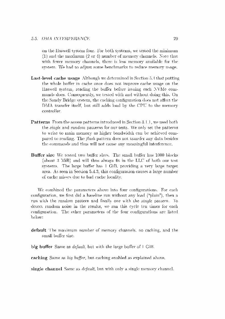
5.5.1 PARSEC
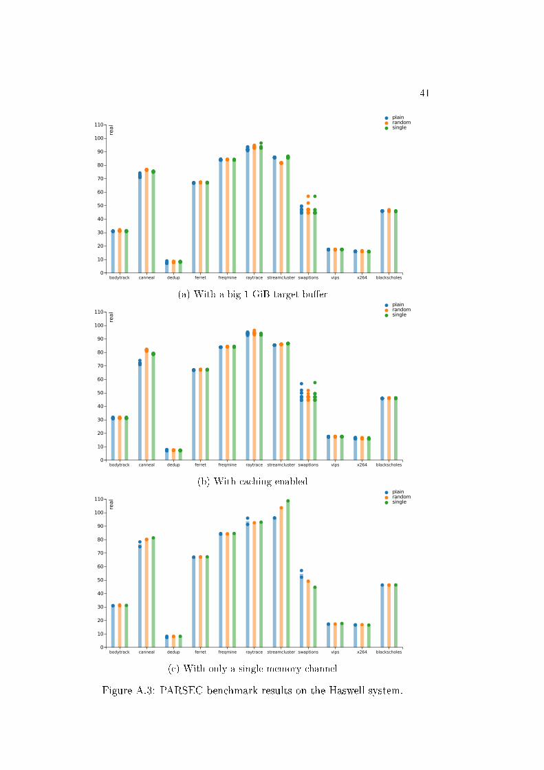
PARSEC is a benchmark suite with a focus on multithreaded applications.Its authors intended its workloads to be similar to real-world tasks [1]. There-fore, it provides a good basis for estimating the impact of high-bandwidthDMA transfers to applications.
The full benchmark results are in Appendix A. Plain is the benchmarkresult without any load, random is with the random pattern, and single iswith the single pattern. The graph bars indicate averages; individual resultsare noted as dots. We measured wall-clock time from launch to exit of thebenchmark programs; the graphs depict the time in seconds.
For most of the benchmarks on both systems, no di�erence is visible whenadding DMA load. The interesting benchmarks that show a di�erence arecanneal, raytrace, and streamcluster. The swaptions benchmark showsa lot of variation, which is not helpful for our analysis; it only shows a cleardi�erence in a single con�guration on Haswell.
(a) Sandy Bridge (b) Haswell
Figure 5.8: Results of the canneal workload.
The canneal benchmark shows an average di�erence of 3.2% on SandyBridge and 2.7% on Haswell when adding either DMA load pattern in thedefault con�guration (Figure 5.8). When increasing the bu�er size to 1 GiB,the di�erence increases to 6.0% on Sandy Bridge; keeping the target bu�er incache does not change this. As DMA transfers never go to the cache on ourSandy Bridge system, we expect the �caching� con�guration to be equivalentto the �big bu�er� one.
On Haswell with the large bu�er, canneal gets slower by 6.5% with therandom pattern and 4.6% with the single pattern. When adding caching, the

5.5. DMA INTERFERENCE 31
di�erence increases signi�cantly to 14% with the random pattern and 10%with the single pattern. This big di�erence to the results on Sandy Bridgecon�rms that DMA transfers work di�erently on the Haswell system due toIntel DDIO.
With only a single memory channel, the random and single pattern resultsdiverge: On Sandy Bridge, the random pattern slows down canneal by 4.2%and the single pattern by 7.4%. On Haswell, the numbers are similar (4.7%and 6.3% respectively).
(a) Sandy Bridge (b) Haswell
Figure 5.9: Results of the raytrace workload.
Figure 5.9 shows the results with the raytrace workload. On both sys-tems, it shows no signi�cant di�erence in the default and single channelcon�gurations.
On the Sandy Bridge system, a slim di�erence of 1.2% is visible with thelarge bu�er and the single pattern, and of 2.0% with caching and the randompattern. On the Haswell system, the di�erence is slightly larger with about1.8% for both patterns in the big bu�er con�guration. When adding caching,this di�erence disappears.
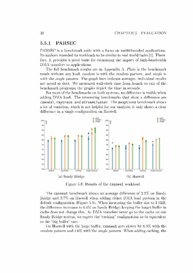
The streamcluster benchmark shown in Figure 5.10 has the biggestdi�erences. On the Sandy Bridge system, there is a di�erence of 5.1% and of5.4% for the random and single patterns in the �rst two con�gurations. Withcaching, this di�erence rises slightly by one percentage point for the randompattern. Limiting to a single memory channel increases the di�erence a lotto 23% for the random pattern and 24% for the single pattern. This suggeststhat the benchmark program is indeed slowed down because of limitations ofthe memory bus.
32 CHAPTER 5. EVALUATION
(a) Sandy Bridge (b) Haswell
Figure 5.10: Results of the streamcluster workload.
In contrast, on the Haswell system (Figure 5.10b), the results are counterto our expectations. While the single pattern shows almost no di�erence tothe plain time, the random pattern actually improves the benchmark resultby 2.5%. With the large bu�er, the improvement doubles to 5.0%. Withcaching enabled, this e�ect disappears and the random and single patternsare slightly slower than the baseline. With only a single memory channel, weget results similar to the Sandy Bridge system. However, the single patternhas a bigger in�uence than the random pattern with 13.2% to 7.9%.
In conclusion, our results coincide with the evaluation of the PARSECauthors (see Section 2.4): The DMA load only a�ects the memory intensiveworkloads. With streamcluster su�ering the most from interference, wewere also able to roughly reproduce their relative ranking.
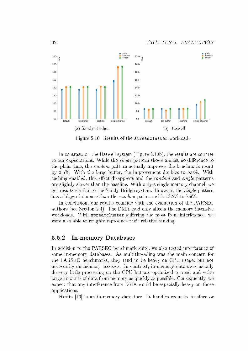
5.5.2 In-memory Databases
In addition to the PARSEC benchmark suite, we also tested interference ofsome in-memory databases. As multithreading was the main concern forthe PARSEC benchmarks, they tend to be heavy on CPU usage, but notnecessarily on memory accesses. In contrast, in-memory databases usuallydo very little processing on the CPU but are optimized to read and writelarge amounts of data from memory as quickly as possible. Consequently, weexpect that any interference from DMA would be especially heavy on thoseapplications.
Redis [16] is an in-memory datastore. It handles requests to store or
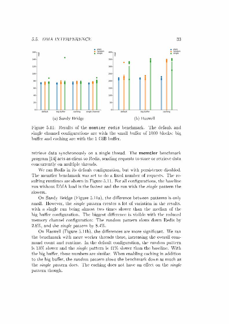
5.5. DMA INTERFERENCE 33
(a) Sandy Bridge (b) Haswell
Figure 5.11: Results of the memtier-redis benchmark. The default andsingle channel con�gurations are with the small bu�er of 1000 blocks; bigbu�er and caching are with the 1 GiB bu�er.
retrieve data synchronously on a single thread. The memtier benchmarkprogram [14] acts as client to Redis, sending requests to store or retrieve dataconcurrently on multiple threads.
We ran Redis in its default con�guration, but with persistence disabled.The memtier benchmark was set to do a �xed number of requests. The re-sulting runtimes are shown in Figure 5.11. For all con�gurations, the baselinerun without DMA load is the fastest and the run with the single pattern theslowest.
On Sandy Bridge (Figure 5.11a), the di�erence between patterns is onlysmall. However, the single pattern creates a lot of variation in the results,with a single run being almost two times slower than the median of thebig bu�er con�guration. The biggest di�erence is visible with the reducedmemory channel con�guration: The random pattern slows down Redis by2.8%, and the single pattern by 8.4%.
On Haswell (Figure 5.11b), the di�erences are more signi�cant. We ranthe benchmark with more worker threads there, increasing the overall com-mand count and runtime. In the default con�guration, the random patternis 13% slower and the single pattern is 41% slower than the baseline. Withthe big bu�er, these numbers are similar. When enabling caching in additionto the big bu�er, the random pattern slows the benchmark down as much asthe single pattern does. The caching does not have an e�ect on the singlepattern though.
34 CHAPTER 5. EVALUATION
Silo [17] is another in-memory database. It is designed to be very e�cienton modern multicore systems, achieving high memory throughput (see Sec-tion 2.5). Silo's source includes a couple of benchmarks; we used the TPC-Cand YCSB benchmarks here.
The TPC-C benchmark, shown in Figure 5.12, shows a lot of noise on ourSandy Bridge system, but is very consistent on the Haswell system. Never-theless, a curious pattern is visible on both systems: with the DMA load,Silo actually gets slightly faster than without DMA load in all con�gurations.On the Haswell system in the default con�guration, Silo is 1.9% faster withthe random pattern and 5.2% faster with the single pattern. The numbersare similar for the big bu�er con�guration. In the caching con�guration, thebenchmark is once again slightly slower with DMA load. With only a singlememory channel, the plain and random times get slower compared to thedefault con�guration, while the single time stays roughly at the same level,increasing the di�erence to 8.2%.
Due to the noise, the di�erences are a lot less visible on the Sandy Bridgesystem (Figure 5.12a). The clearest di�erence is in the single channel con-�guration, where the single pattern speeds up Silo by 17%.
With the YCSB benchmark, the runtimes are all within 1% of each otheron the Haswell system, showing little interference. In contrast, on the SandyBridge system the DMA load speeds up the benchmark again. In the defaultcon�guration, the random pattern makes the benchmark faster by 3.2% andthe single pattern by 13%. Apart from noise, the results are similar withthe big bu�er and single channel con�gurations. When adding caching, thebenchmark with the random pattern also drops down and is 14% faster thanthe baseline. This signi�cant change is curious, as DMA transfers on theSandy Bridge system do not go to the cache (see Section 2.1).
In conclusion, the in-memory databases indeed all show interference fromour arti�cial DMA load. However, the databases often get faster with addedload, which is the opposite of what we expected to see.

5.5. DMA INTERFERENCE 35
(a) Sandy Bridge (b) Haswell
Figure 5.12: Results of the silo-tpcc benchmark.
(a) Sandy Bridge (b) Haswell
Figure 5.13: Results of the silo-ycsb benchmark.

36 CHAPTER 5. EVALUATION
Chapter 6
Conclusion
In this work, we analyzed the in�uence of high-bandwidth DMA transfers onrunning programs. We chose solid-state drives based on NVMe to generatethe synthetic DMA load and used raw NVMe commands to shape tra�cprecisely. This allowed us to simulate access patterns resembling both blockstorage devices (with the random pattern) and networking cards (with thesingle pattern). Making sure that the load generator is only limited byour hardware, we also modi�ed the Linux kernel to eliminate a potentialbottleneck in the NVMe driver; this did however not improve performance.
In our evaluation, we �rst analyzed the DMA bandwidth our load genera-tor can achieve. Using two test systems, we showed the bandwidth di�erencesof PCI Express 2.0 and 3.0, and presented the performance characteristicsof our SSD at di�erent levels of parallelism. We revealed that when aimingfor maximum transfer bandwidth, only two parallel workers are currentlyrequired; this is likely to change with future devices though.
We used Uncore performance counters to further evaluate our syntheticDMA load, showing ways to estimate NVMe command counts as well asdata transfer sizes without modifying the program issuing the commands.Additionally, we were able to see e�ects of Intel's DDIO technology, whichuses the last-level cache as end point of DMA transfers instead of the mainmemory. When working with small amounts of data on an SSD, the mainmemory is never directly involved; this likely improves overall performance.
Finally, we used the PARSEC benchmark as well as the in-memory data-bases Redis and Silo to assess interference with our synthetic DMA load. Wefound that only processes doing very large and frequent memory transfers area�ected at all. Our expectation that DMA transfers would only slow downprocesses was not con�rmed; in fact, several benchmarks showed a signi�cantspeedup.
Our results show that, if contention of memory accesses is a concern�for
37
38 CHAPTER 6. CONCLUSION
example in the situation the MemGuard authors describe in their evaluation[2]�then high-bandwidth DMA transfers will indeed in�uence the runningprocesses as well. A bandwidth reservation system thus should not onlymanage the memory bandwidth that applications use directly, but also thebandwidth used by I/O operations.
6.1 Future Work
This work was mainly concerned with the generation of DMA load. Ourresults with the interference warrant further analysis of the causes. Perfor-mance counters located at the memory controller may help identifying thebottlenecks in the memory system. Especially the benchmarks speeding upwith added DMA load need additional investigation.
In our evaluation, we only used a single solid-state drive per system. Onour Haswell system, the DMA load was only limited by the read and writeperformance of the SSD. Additional tests with multiple DMA devices couldexplore limitations of DMA and the memory bus. Such a setup is interestingbecause of its resemblance with real-world servers receiving requests from anetworking card and serving data from an SSD.
While one of our test systems had two sockets, we did not test any ef-fects from non-uniform I/O access (NUIOA). For our experiments, we alwayspinned both the load generator and the benchmark to the socket the SSD wasconnected to. When the load generator runs on the other socket instead, theDMA I/O �rst has to traverse a QPI link, which may be another bottleneckcausing interference. Additionally, the Intel DDIO technology does not workin this setup [5].

Appendix A
Full PARSEC Results
(a) Sandy Bridge
(b) Haswell
Figure A.1: PARSEC benchmark results in the default con�guration.
39

40 APPENDIX A. FULL PARSEC RESULTS
(a) With a big 1 GiB target bu�er
(b) With caching enabled
(c) With only a single memory channel
Figure A.2: PARSEC benchmark results on the Sandy Bridge system.
41
(a) With a big 1 GiB target bu�er
(b) With caching enabled
(c) With only a single memory channel
Figure A.3: PARSEC benchmark results on the Haswell system.

42 APPENDIX A. FULL PARSEC RESULTS
Bibliography
[1] Christian Bienia. �Benchmarking Modern Multiprocessors.� PhD the-sis. Princeton University, Jan. 2011.
[2] Marco Caccamo et al. �MemGuard: Memory Bandwidth ReservationSystem for E�cient Performance Isolation in Multi-core Platforms.�In: RTAS '13. 2013.
[3] Intel. Data Direct I/O Technology. url: https://www-ssl.intel.com/content/www/us/en/io/direct-data-i-o.html.
[4] Intel. Intel R© CoreTM i7-4790K Processor. url: http://ark.intel.com/products/80807/.
[5] Intel. Intel R© Data Direct I/O Technology (Intel R© DDIO): A Primer.Tech. rep. Feb. 2012. url: http://www.intel.de/content/dam/www/public/us/en/documents/technology-briefs/data-direct-i-o-
technology-brief.pdf.
[6] Intel. Intel R© Xeon R© Processor E3-1230. url: http://ark.intel.com/products/52271/.
[7] Intel. Intel R© Xeon R© Processor E5 and E7 v3 Family Uncore Perfor-mance Monitoring Reference Manual. June 2015. url: https://www-ssl.intel.com/content/www/us/en/processors/xeon/xeon-e5-
v3-uncore-performance-monitoring.html.
[8] Intel. Intel R© Xeon R© Processor E5-2630v3. url: http://ark.intel.com/products/83356/.
[9] Intel. Intel R© Xeon R© Processor E7-8890 v3. url: http://ark.intel.com/products/84685/.
[10] Intel. nvme-cli. url: https://github.com/linux-nvme/nvme-cli.
[11] Intel. Performance Counter Monitor. Dec. 18, 2014. url: https://software . intel . com / en - us / articles / intel - performance -
counter-monitor/.
43

44 BIBLIOGRAPHY
[12] NVM Express 1.2 Speci�cation. 2014-11-03. url: http://www.nvmexpress.org/wp-content/uploads/NVM-Express-1_2-Gold-20141209.pdf.
[13] READV(2) Linux Programmer's Manual. Aug. 19, 2014.
[14] RedisLabs.Memtier Benchmark. url: https://github.com/RedisLabs/memtier_benchmark.
[15] Samsung. NVMe SSD. url: http://www.samsung.com/global/business/semiconductor/product/flash-ssd/nvmessd.
[16] Salvatore San�lippo. Redis. url: http://redis.io/.
[17] Stephen Tu. Silo. url: https://github.com/stephentu/silo.
[18] Stephen Tu et al. �Speedy Transactions in Multicore In-memory Data-bases.� In: SOSP '13. 2013.
[19] Lukas Werling. nvme-memload. url: https://github.com/lluchs/nvme-memload.