AN 394: Using SOPC Builder & DSP Builder Tool Flowapplication-notes.digchip.com/038/38-21287.pdf ·...
45
Altera Corporation 1 AN-394 Application Note 394 Using SOPC Builder & DSP Builder Tool Flow Introduction Video and image processing typically require very high computational power. Given the increasing processing demands, the parallel processing capabilities of Altera ® programmable logic devices (PLDs) make them an attractive implementation option for highly repetitive tasks found in video and imaging functions. Instead of using multiple programmable digital signal processors, a single FPGA with an embedded Nios ® II processor can deliver the requisite level of computing power more cost-effectively, while simplifying board complexity. The edge detection reference design uses a simple Prewitt edge detection algorithm. The edge detection algorithm implementation maps to just nine adders and two subtractors. The reference design illustrates an example in which designers can decide to use several design capture tools together, such as DSP Builder and SOPC Builder. The edge detection reference design is implemented using a combination of hardware and software components. The edge detection module built in DSP Builder is seamlessly integrated into the overall system using the built-in SOPC Builder interface. In addition to the Nios II processor, the edge detection design uses custom peripherals and standard peripherals found in the SOPC Builder library, the Altera library of parameterizable modules (LPM), and custom logic. The targeted device on the Stratix II EP2S180 DSP development board is the Altera EP2S180F1020C3. f For more information on the Stratix II EP2S180 DSP development board, refer to the Stratix II EP2S180 DSP Development Board Reference Manual. DSP Builder is a digital signal processing (DSP) development tool that interfaces The MathWorks industry-leading system-level DSP tool Simulink with the Altera Quartus ® II development software. DSP Builder provides a seamless design flow in which you can perform algorithmic design and system integration in MATLAB and Simulink and then port the design to hardware description language (HDL) files for use in the Quartus II software. The automatically generated HDL files are at the register transfer level (RTL). They are optimized for use in the Quartus II software for rapid prototyping. f For more information on DSP Builder, refer to the DSP Builder User Guide. August 2005, version 1.0
Transcript of AN 394: Using SOPC Builder & DSP Builder Tool Flowapplication-notes.digchip.com/038/38-21287.pdf ·...

Altera Corporation 1AN-394
Application Note 394
Using SOPC Builder& DSP Builder Tool Flow
Introduction Video and image processing typically require very high computational power. Given the increasing processing demands, the parallel processing capabilities of Altera® programmable logic devices (PLDs) make them an attractive implementation option for highly repetitive tasks found in video and imaging functions. Instead of using multiple programmable digital signal processors, a single FPGA with an embedded Nios® II processor can deliver the requisite level of computing power more cost-effectively, while simplifying board complexity.
The edge detection reference design uses a simple Prewitt edge detection algorithm. The edge detection algorithm implementation maps to just nine adders and two subtractors. The reference design illustrates an example in which designers can decide to use several design capture tools together, such as DSP Builder and SOPC Builder.
The edge detection reference design is implemented using a combination of hardware and software components. The edge detection module built in DSP Builder is seamlessly integrated into the overall system using the built-in SOPC Builder interface. In addition to the Nios II processor, the edge detection design uses custom peripherals and standard peripherals found in the SOPC Builder library, the Altera library of parameterizable modules (LPM), and custom logic. The targeted device on the Stratix II EP2S180 DSP development board is the Altera EP2S180F1020C3.
f For more information on the Stratix II EP2S180 DSP development board, refer to the Stratix II EP2S180 DSP Development Board Reference Manual.
DSP Builder is a digital signal processing (DSP) development tool that interfaces The MathWorks industry-leading system-level DSP tool Simulink with the Altera Quartus® II development software. DSP Builder provides a seamless design flow in which you can perform algorithmic design and system integration in MATLAB and Simulink and then port the design to hardware description language (HDL) files for use in the Quartus II software. The automatically generated HDL files are at the register transfer level (RTL). They are optimized for use in the Quartus II software for rapid prototyping.
f For more information on DSP Builder, refer to the DSP Builder User Guide.
August 2005, version 1.0

2 Altera Corporation
Using SOPC Builder & DSP Builder Tool Flow
SOPC Builder is a system development tool, allowing the user to create a Nios II system module complete with a customized set of system peripherals. SOPC Builder automatically creates the bus arbitration logic connecting the individual components together to create an overall system.
f For more information on SOPC Builder, refer to the SOPC Builder User Guide.
The Nios II embedded processor features a general-purpose RISC CPU architecture. The processor can be reconfigured to a different set of peripherals, memories, interfaces, and performance characteristics using the SOPC Builder tool.
f For more information on the Nios II embedded processor, refer to the Nios II Processor Reference Handbook.
When you install the software from the DSP Development Kit, Stratix II Professional Edition CD-ROM, the design files are installed in the directory structure (see Figure 1).

Altera Corporation 3
Introduction
Figure 1. Prewitt Edge Detection Reference Design Directory Structure
This application note describes the Prewitt edge detection reference design. It starts with the following background sections:
■ “Two-Dimensional Filtering” on page 4—Describes the different kinds of two-dimensional filters and how they can be optimized
■ “Background on Edge Detection” on page 7—Describes the different types of edge detectors
■ “Functional Description” on page 9—Describes the components that comprise the Prewitt edge detection reference design
■ “Before You Begin” on page 12—Lists the software required to run the development kit
StratixII_Pro_DSP_Kit-v1.0.0
DocsContains all DSP Development Kit, Stratix II Professional Edition documentation, including board design files and this user guide
Examples
H/W
ReferenceDesigns Contains reference designs for the Stratix II EP2S180 Kit
<path>
Contains the files for the Stratix II EP2S180 DSP development board
Contains examples for the Stratix II EP2S180 DSP development board
Contains hardware examples for the DSP Development Kit, Stratix II Professional Edition
DocContains the Stratix II EP2S180 Kit edge detection reference design documentation
Tool_FlowContains the edge detection reference design files and documentation
QuartusII Contains the designs used for the "Review Integration of Edge Detector Using SOPC Builder" and "Set Up Hardware & Configure EP2S180 Device" sections
Software Contains designs used in the "Review Software Project in Nios II IDE" and "Rebuild & Run the Software Application" sections
SimulinkContains designs used in the "Review & Simulate the Prewitt Edge Detection Design" and "Perform RTL Simulation (Optional)" sections

4 Altera Corporation
Using SOPC Builder & DSP Builder Tool Flow
This application note also provides information on the following:
■ “Review & Simulate the Prewitt Edge Detection Design” on page 13—Review the Prewitt edge detection design using DSP Builder and simulate the design within Simulink
■ “Perform RTL Simulation” on page 17—Perform RTL simulation using the ModelSim-Altera simulation tool
■ “Review Integration of Edge Detector Using SOPC Builder” on page 21—Review the Avalon slave interface for the Prewitt edge detector co-processor in DSP Builder, as well as the final system using SOPC Builder, analyzing the Nios II soft processor and the individual peripherals that make up the system in the Quartus II design software
■ “Set Up Hardware & Configure FPGA” on page 31—Set up the hardware and configure the Stratix II device with the Prewitt edge detection configuration file
■ “Review Software Project in Nios II IDE” on page 34—Review the software project associated with the Prewitt edge detection design using Nios II IDE
■ “Run the Software Application” on page 39—Run the software application and view the Prewitt edge detection results running on the Stratix II DSP development board; as well as Compare the hardware results with the simulation results from “Review & Simulate the Prewitt Edge Detection Design” on page 13 to verify that the design is functioning correctly
Two-Dimensional Filtering
Two-dimensional filters are common for video and imaging applications. Typically, the convolution kernel is moved pixel-by-pixel and line-by-line across the image performing two-dimensional convolution.
Two-dimensional filters can be used for noise removal, image enhancement, and edge detection.
The two dimensional convolution operation is described in the following equation:
Where: g(m,n) = convolution kernel
P(x,y) = original image
),(),(),(' yxPnmgyxP ⊗=
∑ ∑−= −=
−−=N
Nm
N
NnnymxPnmg ),(),(

Altera Corporation 5
Two-Dimensional Filtering
P’(x,y) = filtered image
2N + 1 = size of convolution kernel
Figure 2 shows the implementation of a generic non-symmetric 2-D image filter (see the reference section, item 2). The incoming pixels are shifted through line buffers that create a delay line. The buffer depth depends on the number of pixels in each line of the frame. These delay lines feed the filter array simultaneously with pixels from all the relevant video lines. At each filter node, the pixel is multiplied with the appropriate filter coefficients. All the multiplier results are added together at the adder tree to produce the filter middle point output result. Typically, scaling is applied at the final output.
Figure 2. Implementation of Non-Symmetric Two-Dimensional Filter
The efficiency of the hardware implementation is measured by the number of multipliers. In most cases, the fewer multipliers used, the more efficient the hardware implementation. Using this metric as the measure, the complexity of the non-symmetric filter is proportional to the dimension of the filter m2, where m × m is the size of the convolution kernel.
Significant size optimization can be achieved in the case of symmetric 2-D filters. When symmetry is present, the two data points that share the same filter coefficient are added prior to the multiplication step, saving a multiplication operation. Taking advantage of filter symmetry reduces the number of multipliers by about half. The optimization is even more
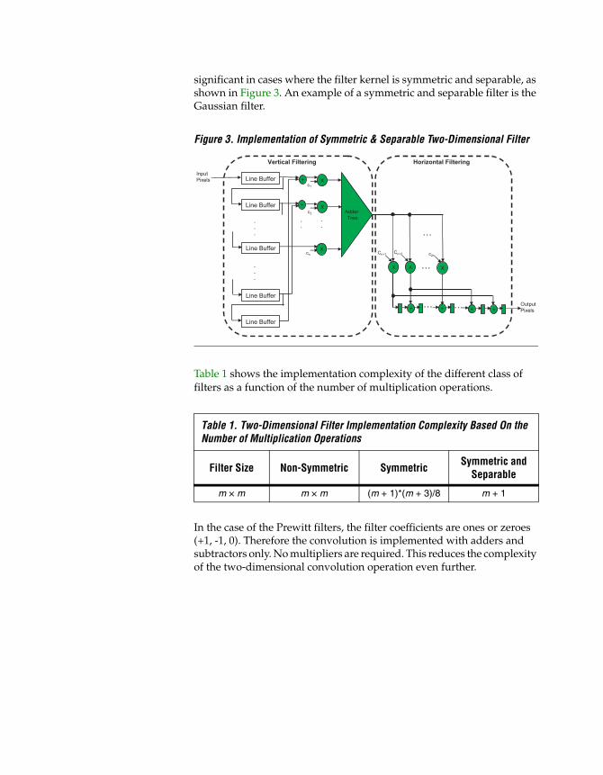
significant in cases where the filter kernel is symmetric and separable, as shown in Figure 3. An example of a symmetric and separable filter is the Gaussian filter.
Figure 3. Implementation of Symmetric & Separable Two-Dimensional Filter
Table 1 shows the implementation complexity of the different class of filters as a function of the number of multiplication operations.
In the case of the Prewitt filters, the filter coefficients are ones or zeroes (+1, -1, 0). Therefore the convolution is implemented with adders and subtractors only. No multipliers are required. This reduces the complexity of the two-dimensional convolution operation even further.
Table 1. Two-Dimensional Filter Implementation Complexity Based On the Number of Multiplication Operations
Filter Size Non-Symmetric Symmetric Symmetric and Separable
m × m m × m (m + 1)*(m + 3)/8 m + 1
XLine Bufferc1
Line Buffer
Line Buffer
.
.
.
Line Buffer
.
.
.
Adder
Tree
Line Buffer
.
.
.
.
Input
Pixels
Output
Pixels
+
+ X
X
c2
cn
X X
…
…
Cn+1 Cn+2 c2n
X
+ + +…
+…
Vertical Filtering Horizontal Filtering
Altera Corporation 7
Background on Edge Detection
Background on Edge Detection
Edge detection is a fundamental tool used in most image processing applications to obtain information from the frames before feature extraction and object segmentation. This process detects outlines of an object and boundaries between objects and the background in the image. An edge detection filter is also used to improve the appearance of blurred or low-pass filtered video streams.
The basic edge detection operator is a matrix area gradient operation that determines the level of variance between different pixels. The edge detection operator is calculated by forming a matrix centered on a pixel chosen as the center of the matrix area. If the value of this matrix area is above a given threshold, then the middle pixel is classified as an edge. Examples of gradient-based edge detectors are Roberts, Prewitt, and Sobel operators. All the gradient-based algorithms have kernel operators that calculate the strength of the slope in directions that are orthogonal to each other, generally horizontal and vertical. Later, the contributions of the different components of the slopes are combined to give the total value of the edge strength.
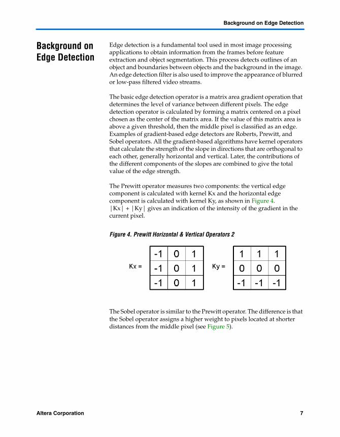
The Prewitt operator measures two components: the vertical edge component is calculated with kernel Kx and the horizontal edge component is calculated with kernel Ky, as shown in Figure 4. |Kx| + |Ky| gives an indication of the intensity of the gradient in the current pixel.
Figure 4. Prewitt Horizontal & Vertical Operators 2
The Sobel operator is similar to the Prewitt operator. The difference is that the Sobel operator assigns a higher weight to pixels located at shorter distances from the middle pixel (see Figure 5).

Figure 5. Sobel Horizontal & Vertical Operators
The gradient-based edge detectors are sensitive to noise. In most cases, you need to apply a low pass filter to the image prior to the edge detection process. The low pass filter has a smoothing effect that reduces the noise, but it also has a negative effect of losing critical information in the image, especially around the edges.
Another class of optimal detectors offer more advanced techniques that are less sensitive to noise and are more adaptable to the local characteristics of the images. These optimal detectors fall into one of two categories: parametric fitting and optimal enhancement [see reference section, item 1]. The parametric fitting technique adjusts the image by an edge model and selects edge pixels based on minimizing the mean square error during the edge fitting process. The optimal enhancement technique defines a set of performance criteria and designs an edge detector that optimizes these criteria.
Altera Corporation 9
Functional Description
Functional Description
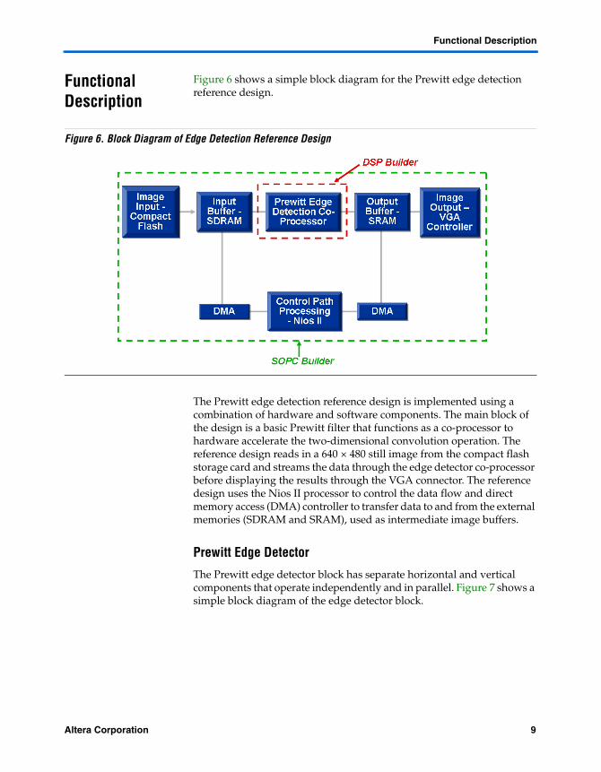
Figure 6 shows a simple block diagram for the Prewitt edge detection reference design.
Figure 6. Block Diagram of Edge Detection Reference Design
The Prewitt edge detection reference design is implemented using a combination of hardware and software components. The main block of the design is a basic Prewitt filter that functions as a co-processor to hardware accelerate the two-dimensional convolution operation. The reference design reads in a 640 × 480 still image from the compact flash storage card and streams the data through the edge detector co-processor before displaying the results through the VGA connector. The reference design uses the Nios II processor to control the data flow and direct memory access (DMA) controller to transfer data to and from the external memories (SDRAM and SRAM), used as intermediate image buffers.
Prewitt Edge Detector
The Prewitt edge detector block has separate horizontal and vertical components that operate independently and in parallel. Figure 7 shows a simple block diagram of the edge detector block.

Figure 7. Block Diagram of Prewitt Edge Detector
The input buffer shifts incoming pixel values through as delay lines. The depth of the line buffer depends on the width of the image size. This design uses an image with a width of 640. The number of line buffers depends on the size of the convolution kernel. This design uses a Prewitt convolution kernel of size 3 × 3 (see Figure 4 on page 7). The implementation of the vertical and horizontal filters is identical. The difference between the filters is in the data streaming through from the input buffer. The results from both components are later combined and a threshold is applied to create a final binary image as the edge detection result. The filter is pipelined where a resulting pixel is calculated every clock cycle.
The edge detector is attached to the Nios II system as a co-processor. The block provides two Avalon slave interfaces: one for transferring the image pixels into the edge detector, and the second for selecting the appropriate edge detection results (pre-threshold or post-threshold) to be transferred to the intermediate data buffer in SDRAM.

Altera Corporation 11
Functional Description
Compact Flash Component
The reference design uses a compact flash component from Microtronix. The core communicates between the compact flash card in True IDE mode and the Nios II system (see Figure 8). The core provides two Avalon slave interfaces: one for accessing the registers on the compact flash device, and the second for the core’s internal register file.
f The compact flash component is downloaded from www.niosforum.com.
Figure 8. Block Diagram of Compact Flash Core
VGA Controller
The VGA controller component drives images with resolution 640 × 480 pixels with 16-bit resolution (see Figure 9). The VGA driver sources its images from either internal or external SRAM/SDRAM. The core provides two Avalon interfaces: one is a DMA controller master that transfers the image line by line from the memory source, and the second is a slave interface that accesses the register bank to configure the DMA controller and the VGA timing circuitry.

Figure 9. Block Diagram of VGA Controller
The other components in the system are standard modules found in the SOPC Builder library.
f For more information on these Nios II peripherals, refer to the Nios II Processor Reference Handbook.
Before You Begin
These instructions assume that you have already installed the software provided with the development kit onto your PC.
f For more information on the software installation, refer to the DSP Development Kit, Stratix II Professional Edition, Getting Started User Guide.
You must have the following software installed on your PC:
■ Quartus II software version 5.0 Service Pack 1■ The MathWorks Release 14 with Service Pack 2 (R14SP2)
● MATLAB version 7.0.4● Simulink version 6.2
■ DSP Builder version 5.0.1 Service Pack 1■ ModelSim-Altera software version 6.0c or ModelSim PE/SE
software version or higher■ Nios II version 5.0

Altera Corporation 13
Review & Simulate the Prewitt Edge Detection Design
1 This application note assumes that you have installed the software into the default locations.
Review & Simulate the Prewitt Edge Detection Design
This section covers the following actions:
■ Review the Prewitt edge detection design■ Simulate the Prewitt edge detection design within Simulink
Review the Prewitt Edge Detection Design
To review the edge detection design, perform the following steps:
1. Run the MATLAB software.
2. In the Current Directory browser, browse to the directory <install_dir>\StratixII_Pro_DSP_Kit-<version> \Examples\HW\ReferenceDesigns\Tool_Flow\Simulink.
3. Choose Open (File menu) and select the file test_sopc_edge_detector.mdl.
4. Review the Simulink design, as shown in Figure 10.
Figure 10. Top Level of Prewitt Edge Detector Design in DSP Builder
5. Double-click the edge_prewitt block to view the underlying hierarchy, which consists of the following components (see Figure 11):
● Image line buffer● Vertical and horizontal Prewitt filters

● Combine and threshold circuit● Data valid circuit
The line buffers shift incoming pixel values through as delay lines. The depth of the line buffer is 640 (width of the image size). The design has a total of three line buffers to accommodate the 3 × 3 convolutional kernel. The Prewitt filter is separated into vertical and horizontal components that operate independently. The results are later combined and a threshold is applied to create a final binary image as the edge detection result. The data valid signal is asserted after the line buffer is filled with one full line of data.
Figure 11. Hierarchy Within Prewitt Edge Detector Design
Simulate the Prewitt Edge Detection Design
To simulate the edge detection design, perform the following steps:

Altera Corporation 15
Review & Simulate the Prewitt Edge Detection Design
1. Choose Configuration Parameters (Simulation menu) to set the Simulink simulation settings (see Figure 12). Because this design uses an image of size 640 × 480, the simulation time is set to 307201 (total number of pixels + 1).
Figure 12. Simulink Simulation Parameters
2. The design uses callback routines during initialization and after simulation stops. To review these callback functions, choose Model Properties and click on the Callbacks tab (File menu) (see Figure 13).
During initialization, the ed_in_script MATLAB script reads in a JPEG image: color.bmp. The script converts the two-dimensional color image data into a one-dimensional gray scale image array: simin. At the end of simulation, the ed_out_script MATLAB script converts the one-dimensional array simulation results from Simulink into a two-dimensional array. The script then plots the original images and the result of the edge detection filter (pre- and post-threshold).

f For more information on callback routines, refer to The MathWorks Using Simulink Manual, available at www.mathworks.com.
Figure 13. Callback Scripts for Simulation
3. Start the simulation by choosing Start (Simulation menu).
At the end of the simulation, the original color, original grayscale, and edge detection results are displayed (see Figure 14).
The bottom left figure shows the result of combining the vertical and horizontal Prewitt filter results. The pixels in the pre-threshold image has the same 8-bit resolution as the input image. The threshold value is selected to be a value at the 90th percentile of cumulative histogram. After applying the threshold to the image, the final edge detection result is a binary image.
4. Close the test_sopc_edge_detector.mdl design.

Altera Corporation 17
Perform RTL Simulation
Figure 14. Edge Detection Results From Simulink
Perform RTL Simulation
This section covers the following actions:
■ Generate simulation files■ Perform RTL simulation with ModelSim■ Compare RTL simulation results with Simulink simulation results
Generate Simulation Files
To generate the simulation files for the Prewitt edge detection design, perform the following steps:
1. Double-click the SignalCompiler block in your model.
2. Click the Analyze tab in the Signal Compiler window.
3. Click the Testbench tab in the Project Setting Options window.
4. Turn on the Generate Stimuli for VHDL Testbench option.

5. Click Convert MDL to VHDL. SignalCompiler generates a simulation script, tb_test_sopc_edge_detector.tcl, and a VHDL testbench that imports the Simulink input stimuli, tb_test_sopc_edge_detector.vhd.
6. Click OK.
7. Run the simulation in Simulink to generate the input stimulus files by choosing Start (Simulation menu).
8. Close the edge detection design file when you are finished generating the input stimulus files.
Perform RTL Simulation in ModelSim
To perform RTL simulation with the ModelSim software, perform the following steps:
1. Start the ModelSim-Altera software.
1 For shorter simulation times, use the ModelSim PE or SE software version 5.8c.
2. Choose Change Directory (File menu).
3. Browse to your working directory <install_dir>\StratixII_Pro_DSP_Kit<version>\Examples\HW\ReferenceDesigns\Tool_Flow\Simulink and click OK.
4. Choose Execute Macro (Tools menu).
5. Browse for the tb_test_sopc_edge_detector.tcl script and click Open.
6. The simulation results are displayed in a waveform (see Figure 15).

Altera Corporation 19
Perform RTL Simulation
Figure 15. ModelSim Waveform Editor with Simulation Results
Compare Simulation Results
During the simulation in Simulink, the To Workspace blocks within the design file (.mdl) export the results to the MATLAB workspace. During the simulation in ModelSim, the VHDL testbench exports the results to text files.
To verify that the RTL simulation results match the Simulink simulation results from “Review & Simulate the Prewitt Edge Detection Design” on page 13, perform the following steps:
1. To compare the simulation results in the MATLAB workspace, use the tbdiff.m file, which is included with the design.
● To compare the pre-threshold results, type the following command in the MATLAB Command window:
>> tbdiff(simout1, 'pre_thresh.txt', 3)
where:
• simout1 is the name of the pre-threshold result from the Simulink simulation.

• pre_thresh.txt is the name of the pre-threshold result from the ModelSim simulation.
● To compare the post-threshold results, type the following command in the MATLAB Command window:
>> tbdiff(simout, 'post_thresh.txt', 3)
where:
• simout is the name of the post-threshold result from the Simulink simulation.
• post_thresh.txt is the name of the post-threshold result from the ModelSim simulation.
1 The tbdiff script compares a MATLAB variable with a text file. The first parameter indicates the MATLAB vector variable (nx1). The second parameter indicates the text file (single column). The third parameter indicates the index to start comparison. If the results are identical, the function returns a 0 (see Figure 16). Otherwise, it returns the number of mismatches.
Figure 16. Compare Simulink & RTL Simulation Results

Altera Corporation 21
Review Integration of Edge Detector Using SOPC Builder
Review Integration of Edge Detector Using SOPC Builder
This section covers the following actions:
■ Review Avalon slave and SOPC Builder interface in DSP Builder■ Review final system using SOPC Builder in the Quartus II software
Review the Avalon Slave & SOPC Builder Interface in DSP Builder
To integrate the edge detector block into the overall system as a SOPC Builder component, you have to add the Avalon interface to the design. The Avalon interface specification defines the transfer interaction between a peripheral and the interconnect logic that connects the component to the rest of the system. The interconnect logic, also known as the Avalon switch fabric, is generated automatically by SOPC Builder. You also need a component description file called class.ptf for use by SOPC Builder. The class.ptf file defines how SOPC Builder integrates the component into the larger system. DSP Builder is highly integrated with SOPC Builder and generates the class.ptf automatically when the option is enabled.
f For more information on custom peripherals, refer to AN333: Developing Peripherals for SOPC Builder.
f For more information on the Avalon switch fabric, refer to the Avalon Bus Specification Reference Manual.
To review the Avalon slave interface, perform the following steps:
1. Choose Open (File menu) and select the file sopc_edge_detector.mdl.
2. Review the Simulink design (see Figure 17).
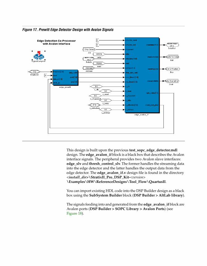
Figure 17. Prewitt Edge Detector Design with Avalon Signals
This design is built upon the previous test_sopc_edge_detector.mdl design. The edge_avalon_if block is a black box that describes the Avalon interface signals. The peripheral provides two Avalon slave interfaces: edge_slv and thresh_control_slv. The former handles the streaming data into the edge detector and the latter handles the output data from the edge detector. The edge_avalon_if.v design file is found in the directory <install_dir>\StratixII_Pro_DSP_Kit-<version> \Examples\HW\ReferenceDesigns\Tool_Flow\QuartusII.
You can import existing HDL code into the DSP Builder design as a black box using the SubSystem Builder block (DSP Builder > AltLab library).
The signals feeding into and generated from the edge_avalon_if block are Avalon ports (DSP Builder > SOPC Library > Avalon Ports) (see Figure 18).

Altera Corporation 23
Review Integration of Edge Detector Using SOPC Builder
Figure 18. Avalon Ports Library in DSP Builder
When you use the Avalon interface’s port blocks in the design, SignalCompiler can generate a peripheral text file (class.ptf) file for use in SOPC Builder. To generate the PTF file, perform the following steps:
1. Double-click the SignalCompiler block.
2. From the SignalCompiler window, click Analyze.
3. Click the right arrow to scroll the tabs to the right.
4. Click the SOPC Info tab (see Figure 19).

Figure 19. SignalCompiler Window
5. Turn on the Generate SOPC Builder PTF File option. When you turn on this option, SignalCompiler generates a class.ptf file for your design that SOPC Builder detects automatically. You will use this class.ptf file in the next section.
6. Choose Use Quartus II Synthesis from the Synthesis Tool list box.
7. Click 1-Convert MDL to VHDL. SignalCompiler generates the VHDL and class.ptf file for the edge detection design. Since you will integrate this custom peripheral into a bigger system using SOPC Builder, the synthesis and fitting process is done within the Quartus II design environment.
8. Close the sopc_edge_detector.mdl design.
Review Final System Using SOPC Builder in Quartus II
In this section, you review the Prewitt edge detection design using SOPC Builder, analyzing the Nios II soft processor and the individual modules that make up the system in the Quartus II design software.
Altera Corporation 25
Review Integration of Edge Detector Using SOPC Builder
The final system includes the following modules:
■ Nios II 32-bit CPU■ External flash memory interface■ External RAM interface■ External RAM bus (Avalon tri-state bridge)■ SDRAM controller■ Compact flash interface (custom peripheral)■ DMA■ Edge detector (custom peripheral from DSP Builder)■ VGA controller (custom peripheral)■ JTAG universal asynchronous receiver/transmitter (UART) ■ Timer■ LED programmed input/output (PIO)■ Button PIO■ 7-segment display PIO■ Dip-switch PIO■ System ID
f For more information on the Nios II processor and peripherals used in this design (except for the custom peripherals), refer to the Nios II Processor Reference Handbook.
To review the Quartus II project that describes the edge detection system, perform the following steps:
1. Run the Quartus II 5.0 Service Pack 1. You can select Yes to get updates automatically from the Altera web site.
2. Choose Open Project (File menu). Browse to the directory <install_dir>\StratixII_Pro_DSP_Kit-<version> \Examples\HW\ReferenceDesigns\Tool_Flow\QuartusII and select the standard.qpf file. The standard.qpf file contains project definitions for the edge detection reference design.
3. Choose Open (File menu) and highlight the standard.bdf file before clicking on Open. This displays the top-level file standard.bdf (see Figure 20).

Figure 20. Top-level File Standard.bdf
4. Choose SOPC Builder (Tools menu). The SOPC Builder window appears (see Figure 21).

Altera Corporation 27
Review Integration of Edge Detector Using SOPC Builder
Figure 21. Final System with Address Map & Nios II System Settings
5. To view the Nios II processor configuration, right-click the cpu block under the Module Name column and select Edit (see Figure 22).

Figure 22. Settings for Nios II Processor
Figure 23 shows the Nios II processor block.
Figure 23. The Nios II Processor Block

Altera Corporation 29
Review Integration of Edge Detector Using SOPC Builder
Table 2 shows the settings for the Nios II processor, cpu.
6. The edge_detector module (located in Avalon Modules > DSP Builder (MATLAB-Simulink) Peripherals > DSP Builder Prewitt Edge Detector) refers to the peripheral generated from the previous section (see Figure 24). The custom peripheral provides two slave interfaces: one for transferring the image pixels into the edge detector (edge_slv), and the second for selecting the appropriate edge detection results (pre-threshold or post-threshold) to be transferred to the data memory in SDRAM (thresh_control_slv).
1 The class.ptf file, which is generated by the SignalCompiler block from the previous section, enabled SOPC Builder to detect the edge detector design and include it as a module in SOPC Builder. The class.ptf file is located in the following directory: <install_dir>\StratixII_Pro_DSP_Kit-<version>\Examples\HW\ReferenceDesigns\Tool_Flow\QuartusII\DSPBuilder_sl.
Table 2. Nios II Processor Setting
Parameter Value
Processor Core Nios II /s (Standard)
Instruction Cache Size 4 Kbytes
JTAG Debug Level 1

Figure 24. Custom Peripherals in Edge Detection System
7. The c_flash module (located in Avalon Modules > Other > CompactFlash Interface) refers to the Compact Flash core from Microtronix that communicates between the compact flash card in True IDE mode and the embedded system (see Figure 24). The core provides two Avalon slave interfaces: one for accessing the registers on the CompactFlash device (ide), and the second for the core’s internal register file (ctl).
f For more information on the CompactFlash core from Microtronix Systems Ltd., refer to www.niosforum.com and click on the Tested IP link.

Altera Corporation 31
Set Up Hardware & Configure FPGA
8. The vga_ controller module (located in Avalon Modules > Other > Altera Avalon 16-bit VGA Driver) is a custom SOPC Builder component that drives images with resolution 640 × 480 pixels with 16-bit resolution (see Figure 24). The VGA driver sources its images from either internal or external SRAM and SDRAM. The core provides two Avalon interfaces: one is a DMA controller master (image_dma_master) that transfers the image line by line from the memory source, and the second is a slave interface (config_slave) that accesses the register bank to configure the DMA controller and the VGA timing circuitry.
9. For all other components, including external memory (Flash, SDRAM, SRAM), DMA, PIO, and UART, you can repeat step 5 above to view the settings for each individual component. These are ready-to-use standard peripherals provided with the Nios II processor.
10. Click Exit to close SOPC Builder after you review the components within the system.
Leave the Quartus II project open for this section.
Set Up Hardware & Configure FPGA
This section covers the following actions:
■ View images on the compact flash card (optional)■ Set up the board for hardware analysis■ Configure the Stratix II device on the Stratix II EP2S180 with the edge
detection design SRAM Object File (.sof)
View Images on Compact Flash Card (Optional)
The software application expects to read the following bitmaps from the CompactFlash card: gray.bmp and color.bmp. The CompactFlash card from the Stratix II DSP development kit is pre-programmed with both bitmaps. The bitmaps are located at:
<install_dir>\StratixII_Pro_DSP_Kit-<version>\example\HW\ReferenceDesigns\Tool_Flow\Simulink\Images
To view the bitmap (.bmp) images on the CompactFlash card, you can use any generic compact flash card reader on your PC.
You can use your own bitmap images with resolution of 640 × 480 after renaming them appropriately.

The design requires two images to be stored in the root directory of the CompactFlash card:
■ RGB color image with 24-bits (8-bits for each color), color.bmp■ Grayscale image with 8-bits, gray.bmp
In the <install_dir>\StratixII_Pro_DSP_Kit-<version> \Examples\HW\ReferenceDesigns\Tool_Flow\Simulink\Images directory, you will find a rgb2gray.m MATLAB script that converts an RGB bitmap to a grayscale BMP.
Set Up the Stratix II EP2S180 DSP Development Board for Hardware Analysis
The hardware analysis requires the power cable, USB Blaster cable, and the CompactFlash card that are included in the kit. To set up the Stratix II EP2S180 DSP development board, perform the following steps:
1. Remove power from the Stratix II DSP development board by disconnecting the power cable.
2. Connect one end of the USB cable to the USB port on your PC. Connect the other end to the 10-pin header labeled (J21) on the Stratix II DSP development board.
3. Remove the CompactFlash card from the Stratix II DSP development board. You need to replug it back after configuring the Stratix II device.
4. Connect one end of the VGA cable to a VGA monitor. Connect the other end to the VGA connector labeled (J35) on the Stratix II DSP development board.
5. Re-apply power to the Stratix II DSP development board.
f For details on installing the USB Blaster software driver on the host PC (located at <quartus_install_dir>\drivers\usb-blaster), see the USB-Blaster Download Cable User Guide.
f For details on components on the Stratix II DSP development board, see the Stratix II EP2S180 DSP Development Board Reference Manual.

Altera Corporation 33
Set Up Hardware & Configure FPGA
Configure the Stratix II Device
To configure the Stratix II device by downloading the SOF image to the DSP development board, perform the following steps:
1. In the Quartus II software, choose Programmer (Tools menu) (see Figure 25).
Figure 25. Quartus II Programming Window
2. Choose Save As (File menu).
3. In the Save As dialog box, type standard.cdf in the File Name box.
4. In the Save As type list, make sure you select Chain Description File.
5. Click Save.
6. In the Mode list of the Programming window, make sure JTAG is selected.
7. Click Hardware Setup to configure the programming hardware. The Hardware Setup dialog box appears.
8. From the Hardware column, select USB Blaster.

9. Click Close to exit the Hardware Setup window.
10. In the Programming window, check the Program/Configure check box on the same line as standard.sof.
11. Click Start. The programmer begins to download the configuration data to the FPGA. The Progress field displays the percentage of data that is downloaded. A message appears when the configuration is complete.
1 If you are not using a licensed version of the Nios II system, a message will appear indicating that you are running a time-limited configuration file on your target hardware.
12. Insert the CompactFlash card face down (the CF symbol faces the board) into the CompactFlash connector header (CON1) on the Stratix II DSP development board. The CompactFlash contains the bitmaps used in “Run the Software Application” on page 39 when you run the software application.
Review Software Project in Nios II IDE
In this section, you review the software project associated with the edge detection design using Nios II IDE. The software project includes the following software source files:
■ FS/—This directory is the placeholder for Micrium’s MicroC/FS (μC/FS) FAT File System including the architecture (port) files for the CompactFlash component.
Due to licensing constraints, the Micrium’s μC/FS source code is not distributed with this reference design. You can run the application using the executable file.
f For more information on the μC/FS FAT File System from Micrium Technologies Corporation, refer to www.micrium.com.
■ main.c—Set up DMA controller to transfer data to/from edge detector. Initiate transfer to VGA controller to output edge detection results. Poll user input through push-buttons and dip switches.
■ read_file.c—Initialize the μC/FS file system and read bitmap from CompactFlash.
■ image.h—Prototype, parameter definitions, and port mapping information.
■ fs_conf.h—Default values and features for building μC/FS FAT file system.
■ fs_port.h—μC/FS architecture (port) file for the Nios II processor.

Altera Corporation 35
Review Software Project in Nios II IDE
■ .cdtbuild—Nios II IDE plug-in default build file. This file provides the include PATHs.
The project uses the μC/FS Fat File System from Micrium Technologies Corporation to access the compact flash. To rebuild the project, you need to download Micrium’s μC/FS source code and unzip the files into the placeholder directory: <install_dir>\StratixII_Pro_DSP_Kit-<version> \Examples\HW\ReferenceDesigns\Tool_Flow\QuartusII\software\ edge_detector\FS.
To review the software code for the edge detection design, perform the following steps:
1. Run the Nios II IDE software by choosing on Start > Programs > Altera > Nios II Development Kit v5.0 > Nios II IDE.
2. Choose Import (File menu) and select the Existing Altera Nios II Project into Workspace from the Import window.
3. Click Next.
4. In the Import Project From File System window, browse to the directory <install_dir>\StratixII_Pro_DSP_Kit-<version> \Examples\HW\ReferenceDesigns\Tool_Flow\QuartusII\ software\edge_detector and click OK (see Figure 26).

Figure 26. Import edge_detector Project
5. Click Finish.
6. When prompted Do you want to remove the project Release and/or Debug directories (recommended)?, click No.
7. Repeat steps 2 through 6 to import the following project: <install_dir>\StratixII_Pro_DSP_Kit-<version>\Examples\HW\ ReferenceDesigns\Tool_Flow\QuartusII\software\ edge_detector_syslib (see Figure 27).

Altera Corporation 37
Review Software Project in Nios II IDE
Figure 27. Import edge_detector_syslib System Library
8. Right-click on the edge_detector_syslib system library located in the C/C++ Projects panel of the Nios II IDE and select Properties.
9. Select System Library from the Properties for edge_detector_syslib dialog box (see Figure 28).
The design uses sdram for the Program, Read-only, and Read/Write memory fields.

Figure 28. System Library Setting for edge_detector_syslib
10. Click Cancel after you review the System Library settings.
11. Right-click on the edge_detector project located in the C/C++ Projects panel of the Nios II IDE and select Properties.
12. Select C/C++ Build from the Properties for edge_detector dialog box (see Figure 29).
The following directories are listed under the Include Paths setting:
../FS
../FS/CLIB
../FS/API
../FS/DEVICE/IDE
../FS/DEVICE/IDE/hardware/nios2_cf
../FS/FS_X
../FS/FSL/fat
../FS/LBL

Altera Corporation 39
Run the Software Application
Figure 29. Project Setting for edge_detector
13. Click Cancel after you review the project settings.
You can review the C source files within the Nios II IDE.
Run the Software Application
The executable file for the software project is included in the design directory. If you have downloaded the μC/FS source code from Micrium Technologies and plan to rebuild the project, follow the instructions in the Rebuild and Run Software Application section. Otherwise, go to the Run Software Application Only section.
Rebuild & Run Software Application (Optional)
The following optional steps are necessary only if you plan to rebuild the project. Before you can rebuild the project, you must first download the μC/FS source code from Micrium Technologies.
1 Due to licensing constraints, the Micrium’s μC/FS source code is not distributed with this reference design.

40 Altera Corporation
Using SOPC Builder & DSP Builder Tool Flow
f For more information on downloading the μC/FS source code from Micrium Technologies, refer to www.micrium.com.
1. Right-click on the edge_detector project in the C/C++ Project window and select Build Project.
2. Choose Run (Run Menu).
3. Select Nios II Hardware from the Configurations: panel in the Run window.
4. Click New.
5. Click the Target Connection tab (see Figure 30).
Figure 30. Nios II Target Connection
6. Set the JTAG cable field to USBBlaster. If necessary click the Refresh button to update the options in the drop-down list.
Altera Corporation 41
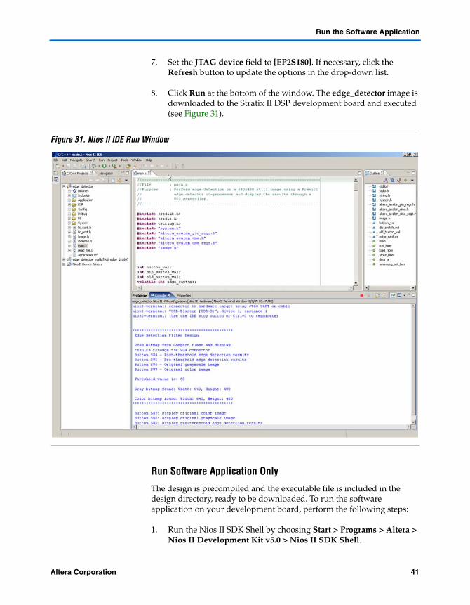
Run the Software Application
7. Set the JTAG device field to [EP2S180]. If necessary, click the Refresh button to update the options in the drop-down list.
8. Click Run at the bottom of the window. The edge_detector image is downloaded to the Stratix II DSP development board and executed (see Figure 31).
Figure 31. Nios II IDE Run Window
Run Software Application Only
The design is precompiled and the executable file is included in the design directory, ready to be downloaded. To run the software application on your development board, perform the following steps:
1. Run the Nios II SDK Shell by choosing Start > Programs > Altera > Nios II Development Kit v5.0 > Nios II SDK Shell.

2. Change the directory to <install_dir>StratixII_Pro_DSP_Kit-<version>\Examples\HW\ReferenceDesigns\Tool_Flow\QuartusII\software\edge_detector\Release by typing the following in the SDK shell:
[SOPC Builder]$ cd <install_dir>/StratixII_Pro_DSP_Kit-<version> /Examples/HW/ReferenceDesigns/Tool_Flow /QuartusII/software/edge_detector/Release r
3. Download the software executable and linkable format file (.elf) to run the program by typing the following in the SDK shell (see Figure 32):
[SOPC Builder]$ ./run.bash r
The executable uses the following command to download the .elf:
nos2-download –cable USBBlaster –g edge_detector.elf
This starts a process that downloads the software, resets the Nios II processor, and starts execution of the software. The development kit push-buttons control which of four images to display through the VGA controller:
● USER_PB3 (SW7) = Original RGB color image● USER_PB2 (SW6) = Original grayscale image● USER_PB1 (SW5) = Edge detection result (pre-threshold)● USER_PB0 (SW4) = Edge detection result (post-threshold)
Compare the hardware results with the simulation results from “Review & Simulate the Prewitt Edge Detection Design” on page 13 to verify that the design is functioning correctly.

Altera Corporation 43
Conclusion
Figure 32. Run Software Applications From SDK Shell
Conclusion The Altera Stratix II device is well suited for implementing imaging functions such as edge detection. The FPGA supports high levels of parallel processing data flow structures that are important for efficient implementation of image processing algorithms. The suite of development tools that include DSP Builder and SOPC Builder allows you to build an imaging function and integrate this peripheral as a coprocessor into the overall system seamlessly.
Troubleshooting This section contains troubleshooting information:
■ Why do I get the following error when simulating the Prewitt edge detection design in DSP Builder: “Error evaluating ‘StopFcn’ callback of block diagram ‘test_sopc_edge_detector’. Attempted to access o(X); index out of bounds because numel(0)=X”?
■ After regenerating the PTF file using SignalCompiler, I noticed there is only one slave interface instead of two.
■ Why do I get errors on missing bitmaps when I run the software application executable (.elf)?

44 Altera Corporation
Using SOPC Builder & DSP Builder Tool Flow
Why do I get the following error when simulating the Prewitt edge detection design in DSP Builder: “Error evaluating ‘StopFcn’ callback of block diagram ‘test_sopc_edge_detector’. Attempted to access o(X); index out of bounds because numel(0)=X”?
At the end of the Simulink simulation, the test_sopc_edge_detector.mdl design calls the ed_out_script that is specified as one of the call back routines. In the output script, it expects an output array of a specific size through the To Workspace blocks. The size of the output array depends on the total simulation time. Specify the stop time (Simulation menu > Configuration Parameters) to be 307201.0 and rerun the simulation.
After regenerating the PTF file using SignalCompiler, I noticed there is only one slave interface instead of two.
When you use the Avalon ports directly in the DSP Builder design and enable the Generate SOPC Builder PTF File option, SignalCompiler automatically generates the PTF file for only one slave interface. In the edge detection co-processor, there are two Avalon slave interfaces. You have to manually edit the PTF file to include a second slave. The modified PTF can be found in the following directory:
<install_dir>\StratixII_Pro_DSP_Kit<version>\Examples\HWReferenceDesigns\Tool_Flow\OuartusII\DSPBuilder_sl
Why do I get errors on missing bitmaps when I run the software application executable (.elf)?
The software application reads the input image from the CompactFlash storage card. It expects two bitmaps of size 640 × 480 resolution with the following names: color.bmp and gray.bmp. Refer to “View Images on Compact Flash Card (Optional)” on page 31 for details.
Also ensure the CompactFlash card is unplugged when you configure the Stratix II device. Refer to “Configure the Stratix II Device” on page 33 for details.
References 1. Ziou D., Tabbone S., “Edge Detection Techniques: An Overview”, Pattern Recognition and Image Analysis, vol. 8, no. 4, 1998
2. Neoh H., Hazanchuk A., “Adaptive Edge Detection for Real-Time Video Processing using FPGAs”, Global Signal Processing, 2004

Altera Corporation 45
101 Innovation DriveSan Jose, CA 95134(408) 544-7000www.altera.comApplications Hotline:(800) 800-EPLDLiterature Services:[email protected]
Copyright © 2005 Altera Corporation. All rights reserved. Altera, The Programmable Solutions Company,the stylized Altera logo, specific device designations, and all other words and logos that are identified astrademarks and/or service marks are, unless noted otherwise, the trademarks and service marks of AlteraCorporation in the U.S. and other countries. All other product or service names are the property of their re-spective holders. Altera products are protected under numerous U.S. and foreign patents and pendingapplications, maskwork rights, and copyrights. Altera warrants performance of its semiconductor productsto current specifications in accordance with Altera's standard warranty, but reserves the right to make chang-es to any products and services at any time without notice. Altera assumes no responsibility or liabilityarising out of the application or use of any information, product, or service describedherein except as expressly agreed to in writing by Altera Corporation. Altera customersare advised to obtain the latest version of device specifications before relying on any pub-lished information and before placing orders for products or services.
References