AN 323: Using SignalTap II Embedded Logic Analyzers in ... · AN-323-1.1 Preliminary Application...
21
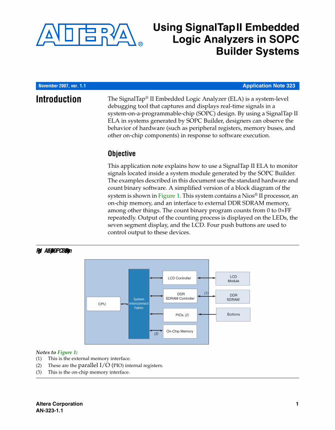
Altera Corporation 1 AN-323-1.1 Preliminary Application Note 323 Using SignalTap II Embedded Logic Analyzers in SOPC Builder Systems Introduction The SignalTap ® II Embedded Logic Analyzer (ELA) is a system-level debugging tool that captures and displays real-time signals in a system-on-a-programmable-chip (SOPC) design. By using a SignalTap II ELA in systems generated by SOPC Builder, designers can observe the behavior of hardware (such as peripheral registers, memory buses, and other on-chip components) in response to software execution. Objective This application note explains how to use a SignalTap II ELA to monitor signals located inside a system module generated by the SOPC Builder. The examples described in this document use the standard hardware and count binary software. A simplified version of a block diagram of the system is shown in Figure 1. This system contains a Nios ® II processor, an on-chip memory, and an interface to external DDR SDRAM memory, among other things. The count binary program counts from 0 to 0×FF repeatedly. Output of the counting process is displayed on the LEDs, the seven segment display, and the LCD. Four push buttons are used to control output to these devices. Fi g u r e 1. An Ex a m p l e SOPC Bu i l d e r Sy s t e m Notes to Figure 1: (1) This is the external memory interface. (2) These are the parallel I/O (PIO) internal registers. (3) This is the on-chip memory interface. LCD Controller CPU PIOs (2) On-Chip Memory DDR SDRAM DDR SDRAM Controller Buttons LCD Module (3) (1) System Interconnect Fabric November 2007, ver. 1.1
Transcript of AN 323: Using SignalTap II Embedded Logic Analyzers in ... · AN-323-1.1 Preliminary Application...
Altera Corporation 1AN-323-1.1 Preliminary
Application Note 323
Using SignalTap II EmbeddedLogic Analyzers in SOPC
Builder Systems
Introduction The SignalTap® II Embedded Logic Analyzer (ELA) is a system-level debugging tool that captures and displays real-time signals in a system-on-a-programmable-chip (SOPC) design. By using a SignalTap II ELA in systems generated by SOPC Builder, designers can observe the behavior of hardware (such as peripheral registers, memory buses, and other on-chip components) in response to software execution.
Objective
This application note explains how to use a SignalTap II ELA to monitor signals located inside a system module generated by the SOPC Builder. The examples described in this document use the standard hardware and count binary software. A simplified version of a block diagram of the system is shown in Figure 1. This system contains a Nios® II processor, an on-chip memory, and an interface to external DDR SDRAM memory, among other things. The count binary program counts from 0 to 0×FF repeatedly. Output of the counting process is displayed on the LEDs, the seven segment display, and the LCD. Four push buttons are used to control output to these devices.
Figure 1. An Example SOPC Builder System
Notes to Figure 1:(1) This is the external memory interface.(2) These are the parallel I/O (PIO) internal registers.(3) This is the on-chip memory interface.
LCD Controller
CPU
PIOs (2)
On-Chip Memory
DDRSDRAM
DDRSDRAM Controller
Buttons
LCDModule
(3)
(1)
SystemInterconnect
Fabric
November 2007, ver. 1.1

2 Altera CorporationPreliminary
Using SignalTap II Embedded Logic Analyzers in SOPC Builder Systems
This application note explains how to connect the SignalTap II Embedded Logic Analyzer to three different types of signals (see Figure 1) that are useful to monitor:
■ Signals connected to an external I/O interface, in this case an external SDRAM memory.
■ Internal registers of a peripheral inside the system module, in this case the PIO.
■ Avalon® interfaces between the System Interconnect Fabric logic and a peripheral inside the system module, in this case an on-chip memory.
This document does not discuss the contents of the standard design example, but you can explore the design in SOPC Builder and refer to the readme.txt in the design directory to gain a better understanding.
System Requirements
To complete the steps in this document, you need the following:
■ Quartus® II software, version 7.2 or higher■ Nios II Embedded Development Suite 7.2 or higher■ Nios II Development Kit, Cyclone® II, or Stratix® II Edition
Design Files
The design files that accompany this application note are included in the examples directory installed with the Nios II Embedded Design Suite. The default location is:
<Altera tools install dir>\<version>\nios2eds\examples
Designing with SignalTap II and SOPC Builder Systems
The following steps guide you through opening a Quartus II project that includes an SOPC Builder-generated system module, and creating a SignalTap II ELA to analyze signals in the system.
Open and Generate the SOPC Builder System
1. Copy the entire folder for the Nios II standard example design for your particular board to a location where it can be edited. This folder is located in the following path:
● If you are using Verilog as your primary HDL: <Altera tools install>/<version>/nios2eds/examples/verilog/<your-nios2-board-type>/standard

Altera Corporation 3Preliminary
Designing with SignalTap II and SOPC Builder Systems
● If you are using VHDL as your primary HDL: <Altera tools install dir>/<version>/nios2eds/examples/vhdl/<your-nios2-board-type>/standard
2. Open the Quartus II software.
3. On the File menu, click Open Project.
4. Browse to the location where you copied the standard example design. Select the NiosII_<board name>_standard.qpf file and click Open.
5. On the Assignments menu, click Settings.
6. In the Settings dialog box, under the Compilation Process Settings section, select Incremental Compilation. Set the Incremental Compilation option to Off as shown in Figure 2.
1 By turning off the Incremental Compilation option, pre-synthesis signals can be added to the SignalTap II ELA in the later sections. Pre-synthesis signals exist after design elaboration, but before any synthesis optimizations are done. This set of signals should reflect your register transfer level (RTL) signals.

4 Altera CorporationPreliminary
Using SignalTap II Embedded Logic Analyzers in SOPC Builder Systems
Figure 2. Compilation Process Settings
7. Click OK.
8. In the Quartus II software, open the Tools menu and select SOPC Builder. The SOPC Builder software opens as shown in Figure 3.
Altera Corporation 5Preliminary
Designing with SignalTap II and SOPC Builder Systems
Figure 3. Example of SOPC Builder System Software
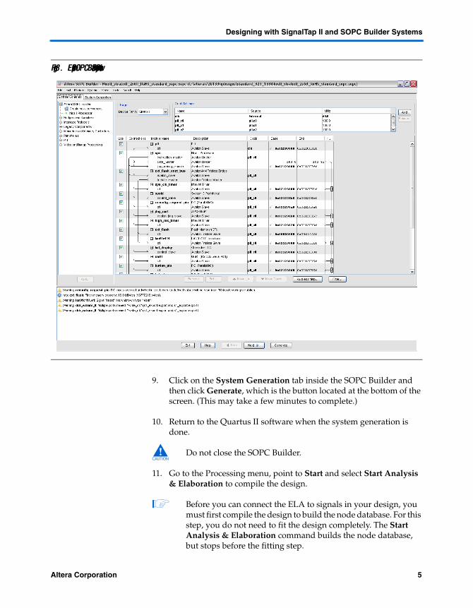
9. Click on the System Generation tab inside the SOPC Builder and then click Generate, which is the button located at the bottom of the screen. (This may take a few minutes to complete.)
10. Return to the Quartus II software when the system generation is done.
c Do not close the SOPC Builder.
11. Go to the Processing menu, point to Start and select Start Analysis & Elaboration to compile the design.
1 Before you can connect the ELA to signals in your design, you must first compile the design to build the node database. For this step, you do not need to fit the design completely. The Start Analysis & Elaboration command builds the node database, but stops before the fitting step.

6 Altera CorporationPreliminary
Using SignalTap II Embedded Logic Analyzers in SOPC Builder Systems
12. Click OK when analysis and elaboration completes successfully.
Create a New Project in Nios II IDE
1. Go to the SOPC Builder and open the SOPC Builder System Generation tab. Click the Nios II IDE button to launch the Nios II IDE software.
2. Open the File menu, point to New and click Project to create a new project.
3. Expand the Altera Nios II Folder and select Nios II C/C++ Application, then click Next.
4. Select Count Binary from the Select Project Template list as shown in Figure 4.
Figure 4. Nios II IDE New Project Wizard
Altera Corporation 7Preliminary
Designing with SignalTap II and SOPC Builder Systems
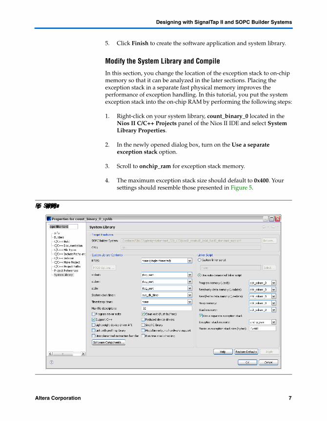
5. Click Finish to create the software application and system library.
Modify the System Library and Compile
In this section, you change the location of the exception stack to on-chip memory so that it can be analyzed in the later sections. Placing the exception stack in a separate fast physical memory improves the performance of exception handling. In this tutorial, you put the system exception stack into the on-chip RAM by performing the following steps:
1. Right-click on your system library, count_binary_0 located in the Nios II C/C++ Projects panel of the Nios II IDE and select System Library Properties.
2. In the newly opened dialog box, turn on the Use a separate exception stack option.
3. Scroll to onchip_ram for exception stack memory.
4. The maximum exception stack size should default to 0x400. Your settings should resemble those presented in Figure 5.
Figure 5. System Library Properties Dialog Box

8 Altera CorporationPreliminary
Using SignalTap II Embedded Logic Analyzers in SOPC Builder Systems
5. Click OK.
6. Right click on count_binary_0 project and select Build Project. This creates the necessary executable and linked format (.elf) file. (This may take a few minutes to complete.)
Create a New SignalTap II File and Add Signals to Monitor
In this section, you create a new SignalTap II file, then add signals to it that you want to monitor.
1. Return to the Quartus II software. On the Tools menu, click SignalTap II Logic Analyzer to bring up the SignalTap II File window.
2. Set the synchronization clock for the ELA in the Signal Configuration area.
a. Click the Browse button next to Clock to bring up the Node Finder.
b. Inside Node Finder, click on the Browse button that is next to the Look in field to bring up the Select Hierarchy Level dialog box.
c. Expand the hierarchy list under NiosII_<board name>_standard_sopc:NiosII_<board name>_standard_sopc_instance by clicking on the “+” icon.
d. In the expanded hierarchy list, click on the entity pll:the_pll.
e. Click OK to close the list.
f. In the Node Finder, click on List to list all of the nodes.
g. Double-click on the node c0 to add it to the Selected Nodes field.
h. Click OK.
3. Specify 256 for the Data Sample depth as shown in Figure 6. Leave the other settings at their default values.

Altera Corporation 9Preliminary
Designing with SignalTap II and SOPC Builder Systems
Figure 6. SignalTap II Signal Configuration Settings
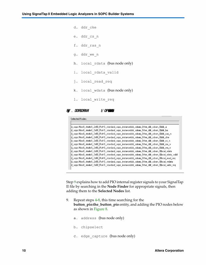
In steps 4-11, you specify the signals you wish to monitor by searching in the Node Finder and adding signals to the Selected Nodes list. The signals to be monitored in this tutorial are selected from three major entities within the system: the interfacing signals for DDR SDRAM, signals within internal registers of PIO, and the signals for on-chip RAM.
Steps 4 - 8 describe how to add DDR SDRAM interfacing signals to your SignalTap II file by searching through the Node Finder and adding the appropriate signals to the Selected Nodes list.
4. In the SignalTap II window, double-click in the Setup area to open the Node Finder. The Node Finder window appears with Filter set to SignalTap II: pre-synthesis.
5. Bring up the Select Hierarchy Level dialog box and search for the entity named ddr_sdram_0:the_ddr_sdram 0.
6. Click OK to close the list.
7. List all the nodes by clicking List in the Node Finder.
8. Add the following nodes to the Selected Nodes list, as shown in Figure 7. Click OK and you return to the SignalTap II window with all the selected signals listed in the Setup area.
a. ddr_a (bus node only)
b. ddr_ba (bus node only)
c. ddr_cas_n
10 Altera CorporationPreliminary
Using SignalTap II Embedded Logic Analyzers in SOPC Builder Systems
d. ddr_cke
e. ddr_cs_n
f. ddr_ras_n
g. ddr_we_n
h. local_rdata (bus node only)
i. local_rdata_valid
j. local_read_req
k. local_wdata (bus node only)
l. local_write_req
Figure 7. DDR SDRAM I/O Pins Selected in the Node Finder
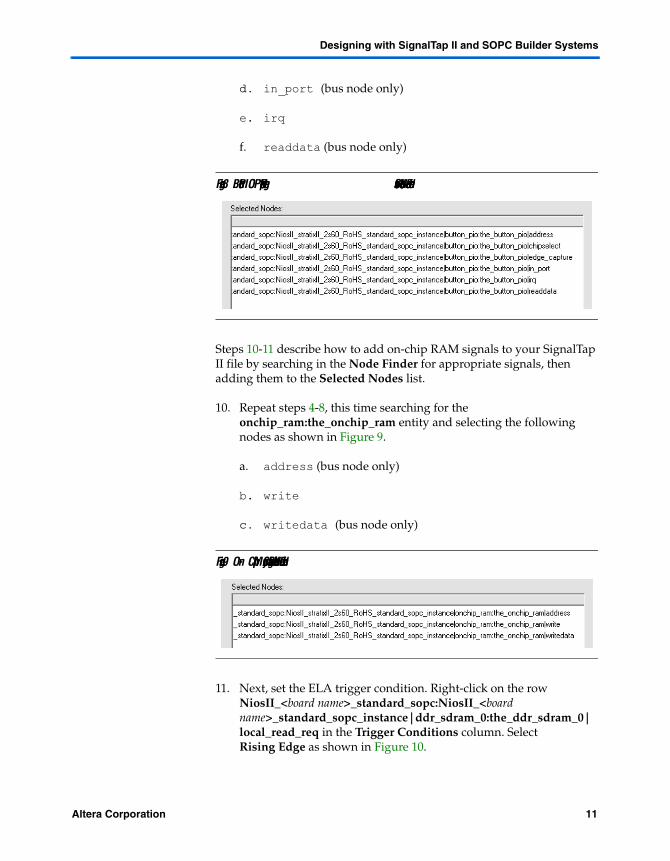
Step 9 explains how to add PIO internal register signals to your SignalTap II file by searching in the Node Finder for appropriate signals, then adding them to the Selected Nodes list.
9. Repeat steps 4-8, this time searching for the button_pio:the_button_pio entity, and adding the PIO nodes below as shown in Figure 8.
a. address (bus node only)
b. chipselect
c. edge_capture (bus node only)
Altera Corporation 11Preliminary
Designing with SignalTap II and SOPC Builder Systems
d. in_port (bus node only)
e. irq
f. readdata (bus node only)
Figure 8. Button PIO Peripheral Registers Selected in the Node Finder
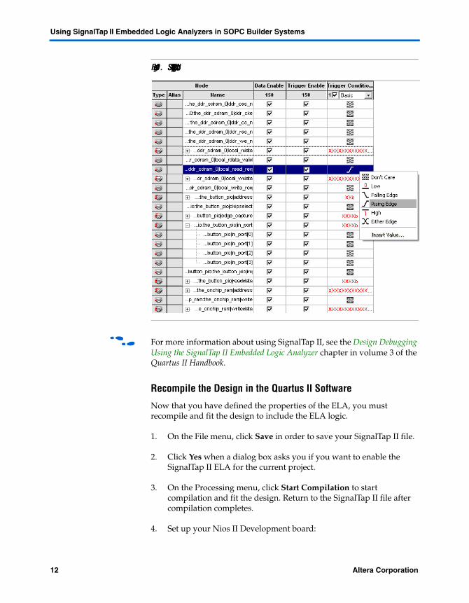
Steps 10-11 describe how to add on-chip RAM signals to your SignalTap II file by searching in the Node Finder for appropriate signals, then adding them to the Selected Nodes list.
10. Repeat steps 4-8, this time searching for the onchip_ram:the_onchip_ram entity and selecting the following nodes as shown in Figure 9.
a. address (bus node only)
b. write
c. writedata (bus node only)
Figure 9. On-Chip Memory Signals Selected in the Node Finder
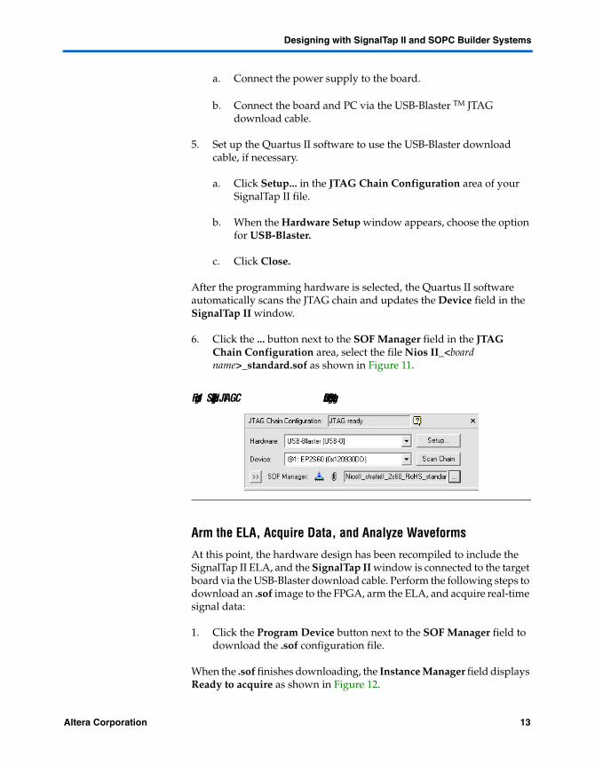
11. Next, set the ELA trigger condition. Right-click on the row NiosII_<board name>_standard_sopc:NiosII_<board name>_standard_sopc_instance|ddr_sdram_0:the_ddr_sdram_0|local_read_req in the Trigger Conditions column. Select Rising Edge as shown in Figure 10.
12 Altera CorporationPreliminary
Using SignalTap II Embedded Logic Analyzers in SOPC Builder Systems
Figure 10. Selecting the Trigger Condition
f For more information about using SignalTap II, see the Design Debugging Using the SignalTap II Embedded Logic Analyzer chapter in volume 3 of the Quartus II Handbook.
Recompile the Design in the Quartus II Software
Now that you have defined the properties of the ELA, you must recompile and fit the design to include the ELA logic.
1. On the File menu, click Save in order to save your SignalTap II file.
2. Click Yes when a dialog box asks you if you want to enable the SignalTap II ELA for the current project.
3. On the Processing menu, click Start Compilation to start compilation and fit the design. Return to the SignalTap II file after compilation completes.
4. Set up your Nios II Development board:
Altera Corporation 13Preliminary
Designing with SignalTap II and SOPC Builder Systems
a. Connect the power supply to the board.
b. Connect the board and PC via the USB-Blaster TM JTAG download cable.
5. Set up the Quartus II software to use the USB-Blaster download cable, if necessary.
a. Click Setup... in the JTAG Chain Configuration area of your SignalTap II file.
b. When the Hardware Setup window appears, choose the option for USB-Blaster.
c. Click Close.
After the programming hardware is selected, the Quartus II software automatically scans the JTAG chain and updates the Device field in the SignalTap II window.
6. Click the ... button next to the SOF Manager field in the JTAG Chain Configuration area, select the file Nios II_<board name>_standard.sof as shown in Figure 11.
Figure 11. SignalTap II JTAG Chain Configuration Settings
Arm the ELA, Acquire Data, and Analyze Waveforms
At this point, the hardware design has been recompiled to include the SignalTap II ELA, and the SignalTap II window is connected to the target board via the USB-Blaster download cable. Perform the following steps to download an .sof image to the FPGA, arm the ELA, and acquire real-time signal data:
1. Click the Program Device button next to the SOF Manager field to download the .sof configuration file.
When the .sof finishes downloading, the Instance Manager field displays Ready to acquire as shown in Figure 12.

14 Altera CorporationPreliminary
Using SignalTap II Embedded Logic Analyzers in SOPC Builder Systems
Figure 12. SignalTap II Instance Manager: Ready to Acquire
2. Click the Run Analysis button to arm the ELA. The Instance Manager field should change to Acquisition in progress as shown in Figure 13.
Figure 13. SignalTap II Instance Manager: Acquisition in Progress
At this point, the ELA is armed and waiting for the trigger condition to occur.
3. In the Nios II IDE, right click on the count_binary_0 project. Point to Run As and click Nios II Hardware as shown in Figure 14.

Altera Corporation 15Preliminary
Designing with SignalTap II and SOPC Builder Systems
Figure 14. Running the Project in Nios II IDE
4. After the program starts running, it triggers the ELA to capture data when there is read operation from the DDR SDRAM memory. In our example, the read operation is performed when the Nios II processor begins executing from DDR SDRAM. The Data tab in the SignalTap II window displays the captured waveforms as shown in Figure 15.

16 Altera CorporationPreliminary
Using SignalTap II Embedded Logic Analyzers in SOPC Builder Systems
Figure 15. Successful Waveform Acquired in SignalTap II Data Tab
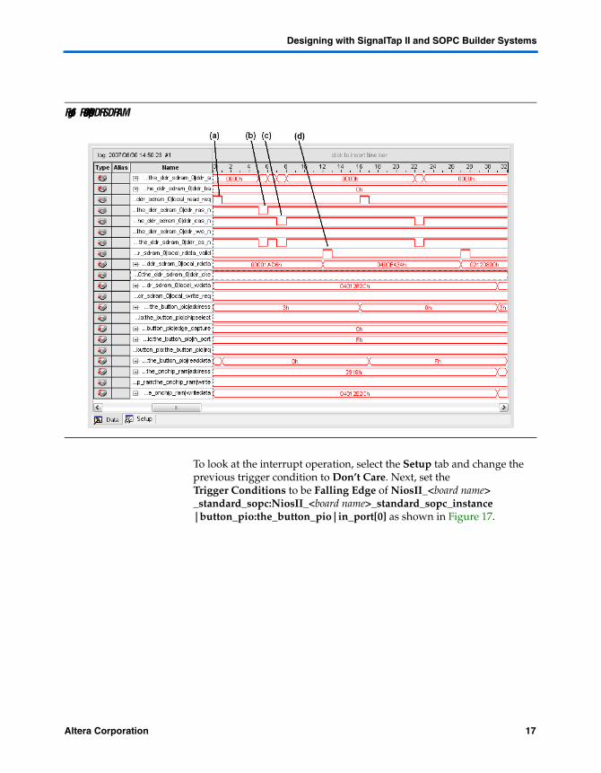
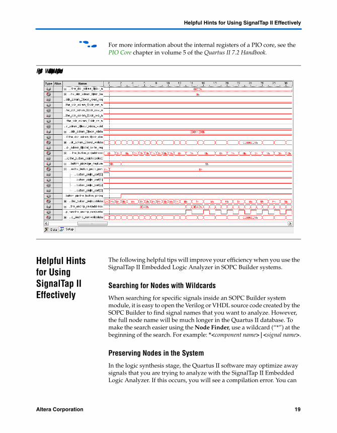
5. Take some time to view the signals. You can left-click the waveforms to zoom in or right-click to zoom out. Figure 16 shows the zoomed in version of the waveform shown in Figure 15. For Figure 16, the read operation can be summarized as follows:
a. The read operation is started by asserting the local_read_req signal.
b. The DDR SDRAM controller issues an active (ACT) command to the SDRAM device to open the SDRAM banks before reading the data from it. This is done by asserting the ddr_ras_n and ddr_cs_n signal.
c. The read (RD) command is issued after that by asserting the ddr_cas_n and ddr_cs_n signal.
d. The controller returns the data requested by asserting the local_rdata_valid signal with the data on the local_rdata bus.
1 Note that the values for some of the address and data buses that you get might vary from what they may look like in Figure 16.
f For more information about the operation of this controller, refer to the DDR and DDR2 SDRAM Controller Compiler User Guide.
Altera Corporation 17Preliminary
Designing with SignalTap II and SOPC Builder Systems
Figure 16. Read Operation of DDR SDRAM
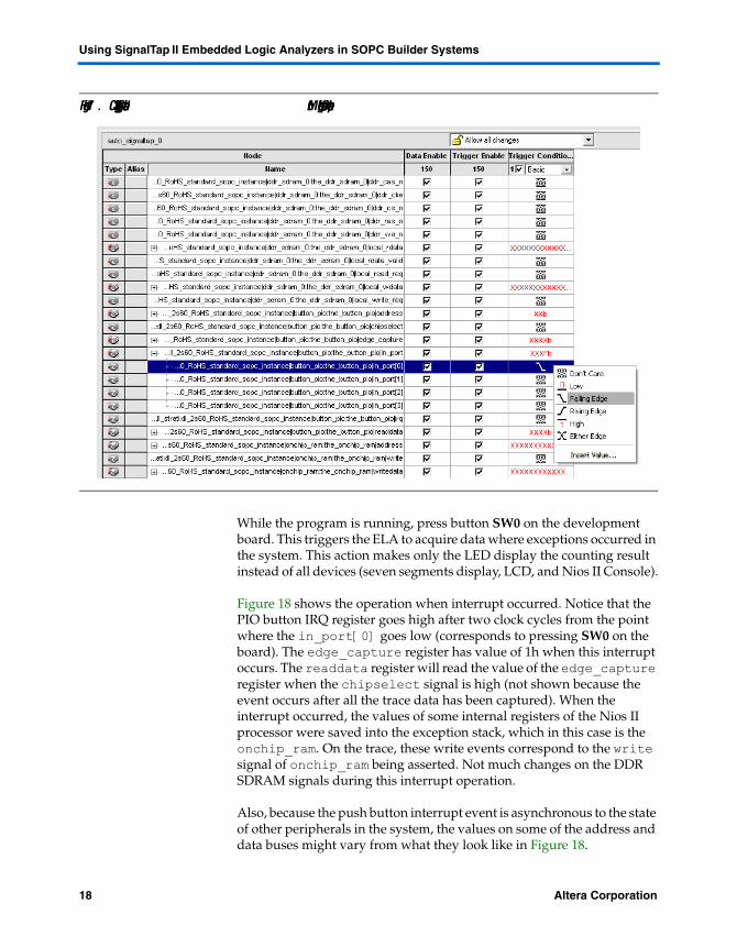
To look at the interrupt operation, select the Setup tab and change the previous trigger condition to Don’t Care. Next, set the Trigger Conditions to be Falling Edge of NiosII_<board name>_standard_sopc:NiosII_<board name>_standard_sopc_instance|button_pio:the_button_pio|in_port[0] as shown in Figure 17.
18 Altera CorporationPreliminary
Using SignalTap II Embedded Logic Analyzers in SOPC Builder Systems
Figure 17. Changing the Trigger Condition for Monitoring Interrupt Operation
While the program is running, press button SW0 on the development board. This triggers the ELA to acquire data where exceptions occurred in the system. This action makes only the LED display the counting result instead of all devices (seven segments display, LCD, and Nios II Console).
Figure 18 shows the operation when interrupt occurred. Notice that the PIO button IRQ register goes high after two clock cycles from the point where the in_port[0] goes low (corresponds to pressing SW0 on the board). The edge_capture register has value of 1h when this interrupt occurs. The readdata register will read the value of the edge_capture register when the chipselect signal is high (not shown because the event occurs after all the trace data has been captured). When the interrupt occurred, the values of some internal registers of the Nios II processor were saved into the exception stack, which in this case is the onchip_ram. On the trace, these write events correspond to the write signal of onchip_ram being asserted. Not much changes on the DDR SDRAM signals during this interrupt operation.
Also, because the push button interrupt event is asynchronous to the state of other peripherals in the system, the values on some of the address and data buses might vary from what they look like in Figure 18.
Altera Corporation 19Preliminary
Helpful Hints for Using SignalTap II Effectively
f For more information about the internal registers of a PIO core, see the PIO Core chapter in volume 5 of the Quartus II 7.2 Handbook.
Figure 18. Waveforms Captured When Interrupt Occurred
Helpful Hints for Using SignalTap II Effectively
The following helpful tips will improve your efficiency when you use the SignalTap II Embedded Logic Analyzer in SOPC Builder systems.
Searching for Nodes with Wildcards
When searching for specific signals inside an SOPC Builder system module, it is easy to open the Verilog or VHDL source code created by the SOPC Builder to find signal names that you want to analyze. However, the full node name will be much longer in the Quartus II database. To make the search easier using the Node Finder, use a wildcard (“*”) at the beginning of the search. For example: *<component name>|<signal name>.
Preserving Nodes in the System
In the logic synthesis stage, the Quartus II software may optimize away signals that you are trying to analyze with the SignalTap II Embedded Logic Analyzer. If this occurs, you will see a compilation error. You can
20 Altera CorporationPreliminary
Using SignalTap II Embedded Logic Analyzers in SOPC Builder Systems
force the Quartus II software to preserve these signals by adding the keep or preserve attribute in the source HDL to the signals you want to monitor.
The keep attribute is used for a wire or net node. For example:
In Verilog:
wire my_wire /* synthesis keep = 1 */:
In VHDL:
signal my_signal: bit;attribute syn_keep : boolean;attribute syn_keep of my_signal: signal is true;
The preserve attribute is used for a register. For example:
In Verilog:
reg my_reg /* synthesis preserve = 1 */:
In VHDL:
signal my_reg: stdlogic;attribute preserve : boolean;attribute preserve of my_signal: signal is true;
Documents Referenced
This document references the following documents:
■ AN 446: Debugging Nios II Systems with the SignalTap II Logic Analyzer■ DDR and DDR2 SDRAM Controller Compiler User Guide■ Design Debugging Using the SignalTap II Embedded Logic Analyzer
chapter, volume 3 of the Quartus II 7.2 Handbook■ PIO Core chapter, volume 5 of the Quartus II 7.2 Handbook

Altera Corporation 21Preliminary
101 Innovation DriveSan Jose, CA 95134www.altera.comTechnical Support:www.altera.com/support/Literature Services:[email protected]
Copyright © 2007 Altera Corporation. All rights reserved. Altera, The Programmable Solutions Company,the stylized Altera logo, specific device designations, and all other words and logos that are identified astrademarks and/or service marks are, unless noted otherwise, the trademarks and service marks of AlteraCorporation in the U.S. and other countries. All other product or service names are the property of their re-spective holders. Altera products are protected under numerous U.S. and foreign patents and pendingapplications, maskwork rights, and copyrights. Altera warrants performance of its semiconductor productsto current specifications in accordance with Altera's standard warranty, but reserves the right to make chang-es to any products and services at any time without notice. Altera assumes no responsibility or liabilityarising out of the application or use of any information, product, or service describedherein except as expressly agreed to in writing by Altera Corporation. Altera customersare advised to obtain the latest version of device specifications before relying on any pub-lished information and before placing orders for products or services.
Revision History
Revision History
Table 1. Document Revision History
Date and Document Version Changes Made Summary of Changes
November 2007 v1.1 ● Updated the sections “Objective”, “System Requirements”, “Design Files”, “Designing with SignalTap II and SOPC Builder Systems”- “Revision History”.
● Updated Figure 1-Figure 18.
Major content additions and updates throughout the bulk of the document.
September 2003 v1.0 Initial Release —