AMD RADEON HD 7970 WITH GRAPHICS CORE NEXT (GCN) ARCHITECTURE … · WITH GRAPHICS CORE NEXT (GCN)...
35
AMD RADEON ™ HD 7970 WITH GRAPHICS CORE NEXT (GCN) ARCHITECTURE Mike Mantor, AMD Senior Fellow [email protected] August 28, 2012
Transcript of AMD RADEON HD 7970 WITH GRAPHICS CORE NEXT (GCN) ARCHITECTURE … · WITH GRAPHICS CORE NEXT (GCN)...

AMD RADEON™
HD 7970
WITH GRAPHICS CORE NEXT (GCN)
ARCHITECTURE
Mike Mantor, AMD Senior Fellow [email protected] August 28, 2012

2 | GCN | HotChips 2012
GRAPHICS CORE NEXT ARCHITECTURE
Product Goals
– Time to Market
– Maximize Performance/Watt
– Enable first class GPU compute
Simplify GPU programming
Improve GPU utilization
Provide predictable performance
Parallel Graphics/Compute Architecture
– New ISA & Compiler
– Distributed Compute Units
– Global Unified Read/Write Cache
– Asynchronous Compute Engines (ACE)
– Reliability improvements with ECC
AMD Eyefinity Display Technology
– Multiple Display Configurations
– 3D Stereo Displays
– Flexible Audio

3 | GCN | HotChips 2012
AMD RADEON™ HD 7970 ARCHITECTURE
Graphic Core Next (GCN)
• 4.3 billion 28nm transistors
4 | GCN | HotChips 2012
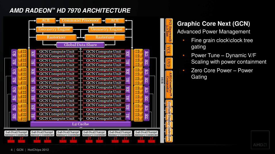
AMD RADEON™ HD 7970 ARCHITECTURE
Graphic Core Next (GCN)
Advanced Power Management
• Fine grain clock\clock tree gating
• Power Tune – Dynamic V/F Scaling with power containment
• Zero Core Power – Power Gating

5 | GCN | HotChips 2012
AMD RADEON™ HD 7970 ARCHITECTURE
Graphic Core Next (GCN)
32 Compute Units(CU)
• Non VLIW ISA
• Distributed Control Flow
• 32/64b IEEE-2008 FP
• Integer, Logic & Video Ops
• 4 Texture Units per CU

6 | GCN | HotChips 2012
AMD RADEON™ HD 7970 ARCHITECTURE
Graphic Core Next (GCN)
• 384-bit GDDR5 - 264GB/Sec
• Unified R/W Cache Hierarchy
• 768KB R/W L2 Cache
• 16KB R/W L1 Per CU
• 16KB Instruction Cache(I$)/4CU
• 32KB Scalar Data Cache(K$)/4CU
7 | GCN | HotChips 2012
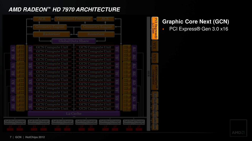
AMD RADEON™ HD 7970 ARCHITECTURE
Graphic Core Next (GCN)
• PCI Express® Gen 3.0 x16

8 | GCN | HotChips 2012
AMD RADEON™ HD 7970 ARCHITECTURE
Graphic Core Next (GCN)
• Global Data Share – 64 kb Shared Memory with global synchronization resources (Barriers, Append, ordered append and named semaphores resources)

9 | GCN | HotChips 2012
Graphic Core Next (GCN)
• Dual Geometry Engines
• Dual Rasterizers
• 8 Render Back-ends
• 32 Pixel Color Raster Operation Pipelines (ROPs)
• 128 Depth Test (Z)/stencil Ops
• Color Cache (C$)
• Depth Cache (Z$)
AMD RADEON™ HD 7970 ARCHITECTURE

10 | GCN | HotChips 2012
Graphic Core Next (GCN)
• Dual Asynchronous Compute Engines (ACE) and Dual DMA
• Compute ECC protection (DRAM & SRAM (Registers, Shared Memories, L1 & L2 Caches)
• GPU support for Compute APIs OpenCLTM1.2, DirectCompute, C++ AMP
AMD RADEON™ HD 7970 ARCHITECTURE

11 | GCN | HotChips 2012
Multi-Media and Display System
• AMD EyeFinity
• Single 16kx16k Image across 6 Displays
• Drives three 3D Stereo Display
• Flexible Bezel Display
• Discrete Digital Multi-Point Audio
• Multi-Display Video Conferencing
• Directional Audio

12 | GCN | HotChips 2012
Multi-Media and Display System Universal Video Decoder (UVD) Fixed Function with codecs for:
• H.264
• VC-1
• MPEG-2 (SD & HD)
• MVC (Blu-ray HD)
• DivX®
• WMV MFT
• WMV native
AMD RADEON™ HD 7970 ARCHITECTURE

13 | GCN | HotChips 2012
AMD RADEON™ HD 7970 ARCHITECTURE
Multi-Media and Display System
Video Codec Engine (Fixed Function)
Multi-stream hardware H.264 HD Encoder
Power efficient & faster than real-time 1080p @60fps
Two encode modes: full fixed & hybrid (with GPU compute)

14 | GCN | HotChips 2012
AMD RADEON™ HD 7970 ARCHITECTURE
Multi-Media and Display System
CrossFireTM Compositor
• Controller for Multi-GPU Solutions
• Dual, triple or quad-GPU scaling

15 | GCN | HotChips 2012
GCN ARCHITECTURE SUPPORTS MULTIPLE PRODUCT CONFIGURATIONS
• Memory Channels/L2 Partitions & I/O Pins
• Vertex/Primitives/Pixel Rates
• Number of Compute Unit and Number Textures
• 64b Floating Point Rates and ECC Options

16 | GCN | HotChips 2012
SPEEDS & FEEDS Dec 2011
AMD Radeon™
HD 7970
Feb 2012
AMD Radeon™
HD 7770
March 2012
AMD Radeon™
HD 7870
June 2012
AMD Radeon™
HD 7970 GHz Edition
Process 28nm 28nm 28nm 28nm
Transistors 4.3 billion 1.5 billion 2.8 billion 4.3 billion
Engine Clock 925 MHz 1000 MHz 1000 MHz 1 GHz / 1.05 GHz
Primitive Rate 2 prim / clk 1 prim / clk 2 prim / clk 2 prim / clk
Stream Processors 2,048 640 1,280 2,048
Compute Performance (SPDP/DPFP)
3.79 TFLOPS / 947 MFLOPS
1.28 TFLOPS / 80 MFLOPS
2.56 TFLOPS / 160 MFLOPS
4.3 TFLOPS / 1.08 TFLOPS
Texture Units 128 40 80 128
Texture Fillrate 118.40 GT/s 40.0 GT/s 80.0 GT/s 134.40 GT/s
ROPS/Pixel Fillrate 32/30.24 GP/s 16/16.0 GP/s 32/32.0 GP/s 32/33.60 GP/s
Z/Stencil 128 64 128 128
Memory Type 3GB GDDR5 2GB GDDR5 2GB GDDR5 3GB GDDR5
Memory Width/Clock 384/1.375 GHz 128/1.125 GHz 256/1.2 GHz 384/1.5 GHz
Memory Data Rate(GDDR5) 5.5 Gbps 4.5 Gbps 4.8 Gbps 6.0 Gbps
Memory Bandwidth 264 GB/s 72 GB/s 153.6 GB/s 288 GB/s
Typical Board Power ~205W ~83W ~150W ~250W
AMD ZeroCore Power <3W <3W <3W <3W

17 | GCN | HotChips 2012
“Pitcairn” HD 78XX “Tahiti” HD 79XX
4.3b transistors 352 SQMM 925e Mhz, 3.78 Tflop 32 CU / 32 Pix / 2 Tri 384b , 5.5gbps, 264 GB/S
2.8b transistors 212 SQMM 1e Ghz, 2.56 Tflop 20 CU / 32 Pix / 2 Tri 256b, 4.8gbps, 154 GB/S
1.5b transistors 123 SQMM 1e Ghz, 1.28 Tflop 10 CU / 16 Pix / 1 Tri 128b, 4.5gbps, 72 GB/S
GCN DISCRETE GPU FAMILY
“Verde” HD 77XX

18 | GCN | HotChips 2012
GCN COMPUTE UNIT
• Basic GPU building block of unified shader system New instruction set architecture
Non-VLIW Vector unit + scalar co-processor Distributed programmable scheduler Unstructured flow control, function calls, recursion, Exception Support Un-Typed, Typed, and Image Memory operations
Each compute unit can execute instructions from multiple kernels simultaneously • Designed for programming simplicity, high utilization, high throughput, with multi-tasking
Branch & Message Unit
Scalar Unit
Vector Units (4x SIMD-16)
Vector Registers (4x 64KB)
Texture Filter Units (4)
Local Data Share (64KB)
L1 Cache (16KB)
Scheduler Texture Fetch
Load / Store Units (16)
Scalar Registers (4KB)
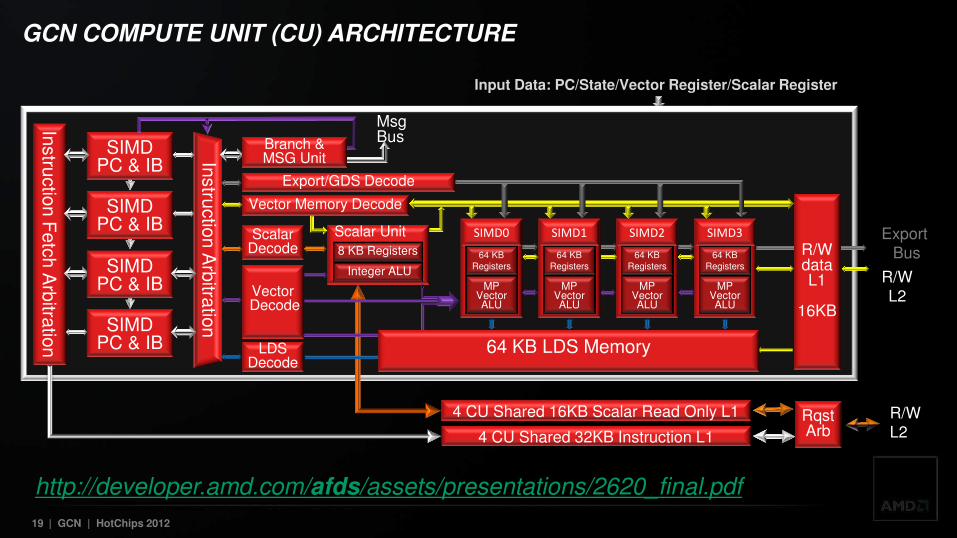
19 | GCN | HotChips 2012
GCN COMPUTE UNIT (CU) ARCHITECTURE
Input Data: PC/State/Vector Register/Scalar Register
SIMD PC & IB
Instru
ctio
n F
etc
h A
rbitra
tion
4 CU Shared 32KB Instruction L1
R/W L2
Instru
ctio
n A
rbitra
tion
4 CU Shared 16KB Scalar Read Only L1 Rqst Arb
Msg Bus
Scalar Decode
Integer ALU
8 KB Registers
Scalar Unit
Vector Decode
Vector Memory Decode
R/W L2
Export/GDS Decode
Export Bus
MP Vector ALU
64 KB Registers
SIMD3
64 KB LDS Memory LDS Decode
MP Vector ALU
64 KB Registers
SIMD0
SIMD PC & IB
SIMD PC & IB MP
Vector ALU
64 KB Registers
SIMD2
SIMD PC & IB
MP Vector ALU
64 KB Registers
SIMD1
Branch & MSG Unit
R/W data L1
16KB
http://developer.amd.com/afds/assets/presentations/2620_final.pdf
20 | GCN | HotChips 2012
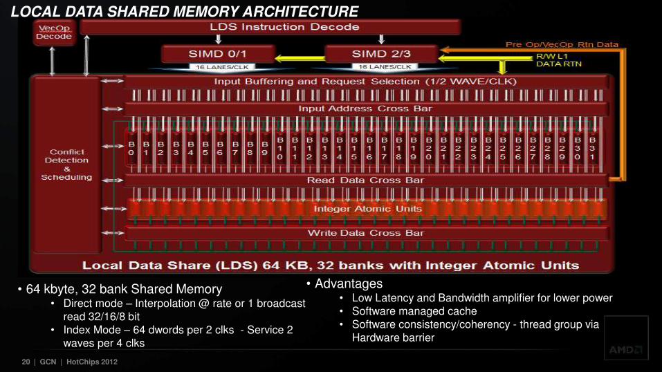
LOCAL DATA SHARED MEMORY ARCHITECTURE
• 64 kbyte, 32 bank Shared Memory • Direct mode – Interpolation @ rate or 1 broadcast
read 32/16/8 bit • Index Mode – 64 dwords per 2 clks - Service 2
waves per 4 clks
• Advantages • Low Latency and Bandwidth amplifier for lower power • Software managed cache • Software consistency/coherency - thread group via
Hardware barrier

21 | GCN | HotChips 2012
Previous AMD GPUs used VLIW (Very Long Instruction Word) architecture
–Combines instructions into a 4-wide VLIW that gets executed on a SIMD
PREVIOUS VLIW SHADER ARCHITECTURE
b + c c + d d + e e + f
a = b + c; b = c + d; c = d + e; d = e + f;
Shader Instructions VLIW Instruction X Y Z W
b + c c + d d + e e + f
b + c c + d d + e e + f
b + c c + d d + e e + f
Thread 0
Thread 1
Thread 2
Thread n

22 | GCN | HotChips 2012
Previous AMD GPUs used VLIW (Very Long Instruction Word) architecture
–Combines instructions into a 4-wide VLIW that gets executed on a SIMD
PREVIOUS VLIW SHADER ARCHITECTURE
b + c idle idle idle
a = b + c; b = a + d; c = b + e; d = c + f;
Shader Instructions VLIW Instruction X Y Z W
b + c idle idle idle
b + c idle idle idle
b + c idle idle idle
Thread 0
Thread 1
Thread 2
Thread n
With Dependencies

23 | GCN | HotChips 2012
Previous AMD GPUs used VLIW (Very Long Instruction Word) architecture
–Combines instructions into a 4-wide VLIW that gets executed on a SIMD
PREVIOUS VLIW SHADER ARCHITECTURE
a + d idle idle idle
a = b + c; b = a + d; c = b + e; d = c + f;
Shader Instructions VLIW Instruction X Y Z W
a + d idle idle idle
a + d idle idle idle
a + d idle idle idle
Thread 0
Thread 1
Thread 2
Thread n
With Dependencies

24 | GCN | HotChips 2012
Previous AMD GPUs used VLIW (Very Long Instruction Word) architecture
–Combines instructions into a 4-wide VLIW that gets executed on a SIMD
PREVIOUS VLIW SHADER ARCHITECTURE
b + e idle idle idle
a = b + c; b = a + d; c = b + e; d = c + f;
Shader Instructions VLIW Instruction X Y Z W
b + e idle idle idle
b + e idle idle idle
b + e idle idle idle
Thread 0
Thread 1
Thread 2
Thread n
With Dependencies

25 | GCN | HotChips 2012
Previous AMD GPUs used VLIW (Very Long Instruction Word) architecture
–Combines instructions into a 4-wide VLIW that gets executed on a SIMD
PREVIOUS VLIW SHADER ARCHITECTURE
c + f idle idle idle
a = b + c; b = a + d; c = b + e; d = c + f;
Shader Instructions VLIW Instruction X Y Z W
c + f idle idle idle
c + f idle idle idle
c + f idle idle idle
Thread 0
Thread 1
Thread 2
Thread n
With Dependencies

26 | GCN | HotChips 2012
SIMD architecture without VLIW instructions
–No need to combine instructions, since multiple threads can run in parallel
NEW NON-VLIW SHADER ARCHITECTURE
b + e b + e b + e
a = b + c; b = a + d; c = b + e; d = c + f;
Shader Instructions ALUs
b + c b + c b + c
a + d a + d a + d
c + f c + f c + f
No idle ALUs due to no dependencies!
b + c
b + e
c + f
a + d
S0 S1 S2 Sn
.... With or without Dependencies

27 | GCN | HotChips 2012
IS VLIW A GOOD LONG TERM SOLUTION?
LANE 0 LANE 1 LANE 2 LANE 15
SIMD
64 Single Precision multiply-add
1 VLIW Instruction × 4 ALU ops dependency limited
Compiler manages register port conflicts
Specialized, complex compiler scheduling
Difficult assembly creation, analysis, and debug
Complicated tool chain support
Careful optimization required for peak performance
VLIW4 SIMD
LANE LANE LANE LANE
SIMD 0 SIMD 1 SIMD 2 SIMD 3
0 1 2 15 0 1 2 15 0 1 2 15 0 1 2 15
64 Single Precision multiply-add
4 SIMDs × 1 ALU op occupancy limited
No register port conflicts
Standardized compiler scheduling & optimizations
Simplified assembly creation, analysis, and debug
Simplified tool chain development and support
Stable and predictable performance
GCN Quad SIMD
VLIW packing sometimes requires domain transformation to achieve good utilization.

28 | GCN | HotChips 2012
CODE EXAMPLE
float fn0(float a,float b) { if(a>b) return((a-b)*a); else return((b-a)*b); }
//Registers r0 contains “a”, r1 contains “b” //Value is returned in r2
v_cmp_gt_f32 r0,r1 //a > b, establish VCC s_mov_b64 s0,exec //Save current exec mask s_and_b64 exec,vcc,exec //Do “if” v_sub_f32 r2,r0,r1 //result = a – b v_mul_f32 r2,r2,r0 //result=result s_andn2_b64 exec,s0,exec //Do “else”(s0 & !exec) v_sub_f32 r2,r1,r0 //result = b – a v_mul_f32 r2,r2,r1 //result = result * b s_mov_b64 exec,s0 //Restore exec mask
• Generally straight forward to generate and understand ISA
• VCC - Vector condition code
• EXEC – Execution mask
• Multi-threaded enables full vector unit utilization

29 | GCN | HotChips 2012
GCN SCALAR/VECTOR COMPUTE UNIT
Simpler ISA compared to previous generation
– No clauses and latency for transitions
– No VLIW packing required
– Control flow directly programmed (Exec mask control)
– Complex Control Flow Supported (Example: non uniform Branch into loop)
Scalar engine
– Lower latency for distributed sequencer verses previous centralized
– Reduces performance in previously clause bound cases
– Reduces power handling of control flow Ops as control is closer
Advanced language feature support
– Exception support
– Function calls
– Recursion
Enhanced extended ALU operations
– Media ops
– Integer ops
– Integer atomic operations
– Floating point atomics (min, max, cmpxchg)
Enhanced debug support
– HW functionality to improve debug support

30 | GCN | HotChips 2012
R/W CACHE HIERARCHY
L2
L1 read/write 16kb write through caches
64 Bytes / CU / clock
L2 read/write cache partitions (64kb/128kb) write back caches
64 Bytes / partition / clock
Each CU has 256kb registers and 64kb local data share
K$ I$ 16KB instruction cache (I$) + 32 KB scalar data cache (K$)
shared per 4 CUs with L2 backing
K$ I$
GDS
Global data share facilitates synchronization between CUs
L2 L2
K$
L1 L1 L1 L1 L1 L1 L1 L1 L1
64b Dual Channel Memory Controller
64b Dual Channel Memory Controller
64b Dual Channel Memory Controller

31 | GCN | HotChips 2012
GPU MEMORY MODEL
Relaxed memory model
– All work-items within same work groups see same L1 cache
– Work-items of different work groups may use different L1 caches
– All work-items and command streams use the same L2 cache
– Command stream packets & Shader Instruction control data visibility
– Sufficient primitives in the GPU hardware to implement C++ 11 memory model
GPU Coherency
– Acquire/Release semantics control data visibility across the machine (Compiler controlled bit on load/store instructions)
– L2 coherent all CUs & CP can have the same view of memory
Remote Global atomics
– Performed in L2 cache
– Full set of integer ops and float max, min, cmp_swap
32 | GCN | HotChips 2012
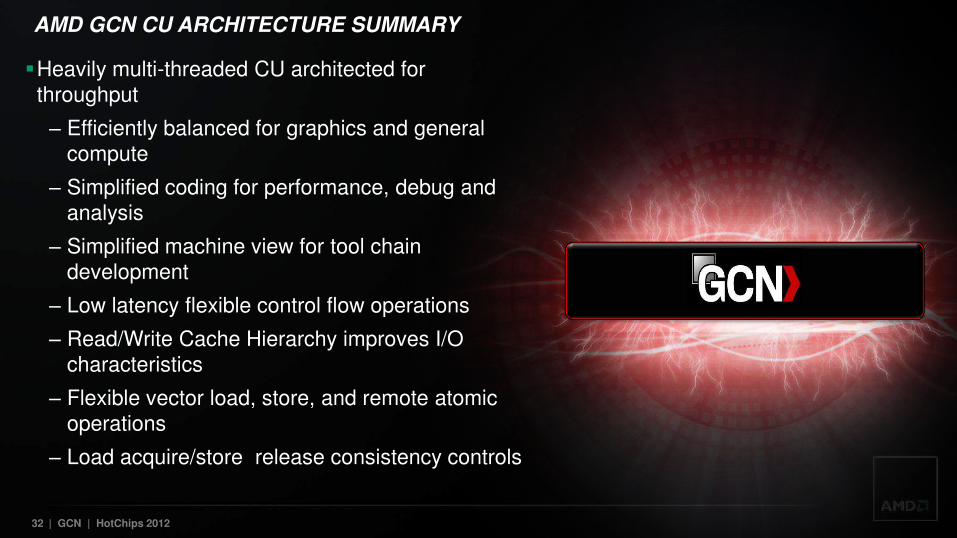
AMD GCN CU ARCHITECTURE SUMMARY
Heavily multi-threaded CU architected for throughput
– Efficiently balanced for graphics and general compute
– Simplified coding for performance, debug and analysis
– Simplified machine view for tool chain development
– Low latency flexible control flow operations
– Read/Write Cache Hierarchy improves I/O characteristics
– Flexible vector load, store, and remote atomic operations
– Load acquire/store release consistency controls
33 | GCN | HotChips 2012
REFERENCE
AMD Display Technologies whitepaper AMD Eyefinity Technology whitepaper AMD Power Technologies whitepaper AMD Video Technologies whitepaper Graphics Core Next Architecture whitepaper
http://www.amd.com/us/products/desktop/graphics/7000/7970/Pages/radeon-7970.aspx#/1
http://developer.amd.com/afds/assets/presentations/2620_final.pdf

34 | GCN | HotChips 2012
float fn0(float a,float b) { if(a>b) return((a-b)*a); else return((b-a)*b); }
Optional: Use based on the number of instruction in conditional section. Executed in branch unit
• Generally straight forward to generate and understand ISA
• Instructions types interleave within program
• Throughput optimized for vector instructions
• Optional scalar instructions jump fully predicated groups of instructions
CODE EXAMPLE
//Registers r0 contains “a”, r1 contains “b” //Value is returned in r2
v_cmp_gt_f32 r0,r1 //a > b, establish VCC s_mov_b64 s0,exec //Save current exec mask s_and_b64 exec,vcc,exec //Do “if” s_cbranch_vccz label0 //Branch if all lanes fail v_sub_f32 r2,r0,r1 //result = a – b v_mul_f32 r2,r2,r0 //result=result * a
label0:
s_andn2_b64 exec,s0,exec //Do “else”(s0 & !exec) s_cbranch_execz label1 //Branch if all lanes fail v_sub_f32 r2,r1,r0 //result = b – a v_mul_f32 r2,r2,r1 //result = result * b
label1: s_mov_b64 exec,s0 //Restore exec mask

35 | GCN | HotChips 2012
Disclaimer & Attribution
The information presented in this document is for informational purposes only and may contain technical inaccuracies, omissions and typographical errors.
The information contained herein is subject to change and may be rendered inaccurate for many reasons, including but not limited to product and roadmap changes, component and motherboard version changes, new model and/or product releases, product differences between differing manufacturers, software changes, BIOS flashes, firmware upgrades, or the like. There is no obligation to update or otherwise correct or revise this information. However, we reserve the right to revise this information and to make changes from time to time to the content hereof without obligation to notify any person of such revisions or changes.
NO REPRESENTATIONS OR WARRANTIES ARE MADE WITH RESPECT TO THE CONTENTS HEREOF AND NO RESPONSIBILITY IS ASSUMED FOR ANY INACCURACIES, ERRORS OR OMISSIONS THAT MAY APPEAR IN THIS INFORMATION.
ALL IMPLIED WARRANTIES OF MERCHANTABILITY OR FITNESS FOR ANY PARTICULAR PURPOSE ARE EXPRESSLY DISCLAIMED. IN NO EVENT WILL ANY LIABILITY TO ANY PERSON BE INCURRED FOR ANY DIRECT, INDIRECT, SPECIAL OR OTHER CONSEQUENTIAL DAMAGES ARISING FROM THE USE OF ANY INFORMATION CONTAINED HEREIN, EVEN IF EXPRESSLY ADVISED OF THE POSSIBILITY OF SUCH DAMAGES.
AMD, the AMD arrow logo, AMD Radeon and combinations thereof are trademarks of Advanced Micro Devices, Inc. All other names used in this presentation are for informational purposes only and may be trademarks of their respective owners.
OpenCL is a trademark of Apple Inc. used with permission by Khronos.
DirectX is a registered trademark of Microsoft Corporation.
DivX is a registered trade mark of DivX Inc
PCI Express is a registered trademark of PCI-SIG
© 2012 Advanced Micro Devices, Inc. All rights reserved.