Quartus II Version 6.0 Handbook, Volume 5: Altera Embedded ...
Altera Embedded SystemsDevelopment Kit, Cyclone III Edition
101 Innovation DriveSan Jose, CA 95134(408) 544-7000http://www.altera.com
User Guide
Document Date: July 2010P25-36348-01

© 2010 Altera Corporation. All rights reserved. ALTERA, ARRIA, CYCLONE, HARDCOPY, MAX, MEGACORE, NIOS, QUARTUS and STRATIX areReg. U.S. Pat. & Tm. Off. and/or trademarks of Altera Corporation in the U.S. and other countries. All other trademarks and service marks are theproperty of their respective holders as described at www.altera.com/common/legal.html. Altera warrants performance of its semiconductor productsto current specifications in accordance with Altera's standard warranty, but reserves the right to make changes to any products and services at anytime without notice. Altera assumes no responsibility or liability arising out of the application or use of any information, product, or service describedherein except as expressly agreed to in writing by Altera. Altera customers are advised to obtain the latest version of device speci-fications before relying on any published information and before placing orders for products or services.
ii Altera CorporationJuly 2010
Part Number UG-01054-1.1
Altera Corporation July 2010 PreliminaryA
Contents
Chapter 1. About This KitIntroduction ............................................................................................................................................ 1–1Key Features and Benefits .................................................................................................................... 1–1About the Development Board ............................................................................................................ 1–3
Hardware Features ........................................................................................................................... 1–3Factory design: the Application Selector ...................................................................................... 1–5Max II CPLD on the Cyclone III FPGA ......................................................................................... 1–5Max II CPLD on LCD Multimedia HSMC .................................................................................... 1–5
About this User Guide .......................................................................................................................... 1–6Before You Begin ................................................................................................................................... 1–7Inspect the board ................................................................................................................................... 1–7
Chapter 2. Software InstallationInstalling the Quartus II Web Edition Software ............................................................................... 2–1
Licensing Considerations ................................................................................................................ 2–2Installing the Altera Embedded Systems Development Kit, Cyclone III Edition ....................... 2–3Licensing IP ............................................................................................................................................ 2–4
Shipping Vs. OpenCore Plus IP Licensing ................................................................................... 2–4Development Kit IP Requirements ................................................................................................ 2–5Embedded IP Suite ........................................................................................................................... 2–5Altera Megacore IP Base Suite ........................................................................................................ 2–5Registering IP licenses ..................................................................................................................... 2–6
Purchasing Software tools and Operating systems .......................................................................... 2–6Nios II C2H Compiler ...................................................................................................................... 2–6Micrium MicroC/OS-II RTOS ........................................................................................................ 2–7NicheStack TCP/IP Network Stack, Nios II Edition ................................................................... 2–7
Chapter 3. Development Board SetupInstructions ............................................................................................................................................. 3–1Requirements ......................................................................................................................................... 3–1Powering Up the Board ........................................................................................................................ 3–1Run the Application Selector ............................................................................................................... 3–2In system update via SD Card: How it works ................................................................................... 3–3Get the latest Ready-to-Run Demos .................................................................................................... 3–4Add your own applications from the LCD touch panel using the Application Selector ............ 3–4Programming Flash with Custom FPGA Configuration ................................................................. 3–4Restoring the Factory Design to the Flash device ............................................................................. 3–5
iiiltera Embedded Systems Development Kit, Cyclone III Edition

Contents
Chapter 4. Remote System Update Via EthernetAbout Remote System Update ............................................................................................................ 4–1Remote System Update: How it works .............................................................................................. 4–1
Requirements .................................................................................................................................... 4–2Operating Instructions for Remote System Update ........................................................................ 4–2Creating Flash Files for Remote System update .............................................................................. 4–3
Chapter 5. Ready-to-Run ApplicationsAbout Ready-to-Run applications ...................................................................................................... 5–1Where to get the latest Ready-to-Run SD Card Demo Applications ............................................. 5–2How to update your SD Card with Ready-to-Run Applications ................................................... 5–2Where to find the Ready-to-Run demos on the SD Card ................................................................ 5–3What’s in a Ready-to-Run Application? ............................................................................................ 5–4Creating your own Ready-to-Run Applications ............................................................................... 5–5
Chapter 6. Example Processor SystemsAbout the Example Processor Systems .............................................................................................. 6–1
Purpose .............................................................................................................................................. 6–1Examples ............................................................................................................................................ 6–1Where to find .................................................................................................................................... 6–1Benefits ............................................................................................................................................... 6–1
About the Nios II 3C120 General Purpose Microprocessor System .............................................. 6–1Location ............................................................................................................................................. 6–1Description ........................................................................................................................................ 6–2IP licenses required to Ship design ................................................................................................ 6–2Nios II 3C120 General Purpose Microprocessor System Description ...................................... 6–2
About the Nios II 3C120 Microprocessor System with LCD Controller ....................................... 6–4Location ............................................................................................................................................. 6–4Description ........................................................................................................................................ 6–4IP licenses required to ship design ................................................................................................ 6–4Nios II 3C120 Microprocessor System with LCD Controller System Description ................. 6–4
Chapter 7. Example Software ApplicationsAbout the Software Applications ........................................................................................................ 7–1About the Application Selector ........................................................................................................... 7–1
Based on processor system ............................................................................................................. 7–1Location ............................................................................................................................................. 7–1Description ........................................................................................................................................ 7–1IP licenses required to ship design ................................................................................................ 7–2Software and middleware licenses required to ship design ...................................................... 7–2
Altera Corporation Development Board Version 1.0.ivJuly 2010 Altera Embedded Systems Development Kit, Cyclone III Edition
Contents
Chapter 8. Application Selector DetailsHardware Images ................................................................................................................................. 8–1Software Images .................................................................................................................................... 8–1CFI Flash ................................................................................................................................................ 8–1Application Boot Code ......................................................................................................................... 8–2Flash Hardware Image Catalog .......................................................................................................... 8–2Hardware Image Caching ................................................................................................................... 8–3Building Application Selector from Source Files ............................................................................. 8–4
Build the project ................................................................................................................................ 8–4Build the boot code ......................................................................................................................... 8–5
Modifying the Application Selector .................................................................................................... 8–5Application Selector Changing the CFI flash map ..................................................................... 8–5General Guidelines .......................................................................................................................... 8–5Application Selector Hardware Image ......................................................................................... 8–6Application Hardware Images ...................................................................................................... 8–6Application Selector Software Image ........................................................................................... 8–6Application Software Image .......................................................................................................... 8–6Flash Catalog ..................................................................................................................................... 8–7About the Webserver ....................................................................................................................... 8–8
Chapter 9. Using the Nios II C2H CompilerHardware Acceleration using Nios II C2H Compiler ...................................................................... 9–1
Features .............................................................................................................................................. 9–1Examples ............................................................................................................................................ 9–1Where to find .................................................................................................................................... 9–1How are demos different from design examples? ...................................................................... 9–2
Altera Mandelbrot C2H Demo ............................................................................................................ 9–2Based on processor system ............................................................................................................. 9–2Location ............................................................................................................................................. 9–2Description ........................................................................................................................................ 9–2IP licenses required to ship design: ............................................................................................... 9–2Software and middleware licenses required to ship design: ..................................................... 9–2Software tools required to ship your hardware accelerators: .................................................... 9–2About the Mandelbrot Set ............................................................................................................... 9–3Using the Mandelbrot application ................................................................................................. 9–3Operation ........................................................................................................................................... 9–6
Chapter 10. Developing USB and SD Card based SystemsUSB Host and Device Controller IP Core ................................................................................... 10–1USB Reference Design ................................................................................................................... 10–1SD Host Controller IP Core ........................................................................................................... 10–1
Using the example designs without the SD Card IP ...................................................................... 10–2LCD Multimedia HSMC SD Card Modes ........................................................................................ 10–2
LCD HSMC Reference Manual .................................................................................................... 10–2LCD HSMC Max II design ............................................................................................................ 10–2Setting LCD HSMC Modes on Max II ......................................................................................... 10–2
v Development Board Version 1.0. Altera CorporationAltera Embedded Systems Development Kit, Cyclone III Edition July 2010
Contents
Chapter 11. Restoring the Factory Design to the Flash DeviceRestoring the Original Flash Image (Application Selector) ........................................................... 11–1Rebuilding the Application Selector from Source Files ................................................................. 11–2
Boot Code ........................................................................................................................................ 11–3Hardware Image Catalog ............................................................................................................. 11–3Application Selector Hardware Image ....................................................................................... 11–4Application Selector Software Image .......................................................................................... 11–4
Combining factory recovery image files .......................................................................................... 11–5
Appendix A. Frequently Asked QuestionsWhy do I get the error “Can't find valid feature line for core SD_MMC_SPI_CORE (EC11_0002) in current license; Error: Error (10003): Can't open encrypted VHDL or Verilog HDL file” when I try to re-generate the LCD or Application Selector hardware design? ........................................................................................................................... A–1Where can I get the SD-Card Controller IP License? ................................................................. A–1I have pictures that I would like to display on the PlanetWeb Digital Photo Frame. How do I do that? ............................................................................................................. A–1How do I add my own design so the Application Selector can find and run it? .................. A–2Where do I go to get more designs for the Altera Embedded Systems Development Kit? ............................................................................................................................ A–2How do I open a design example in the Nios II IDE? ............................................................... A–2I overwrote the Flash with my own design. But now I want to restore the original contents of the flash, the one that came when the board was shipped. How do I restore the factory image? .......................................................................................................................... A–3How do I re-build the factory image from source files? ........................................................... A–3
Additional InformationRevision History ......................................................................................................................................... iHow to Contact Altera ............................................................................................................................... iFurther Information ................................................................................................................................. iiTypographic Conventions ....................................................................................................................... ii
Altera Corporation Development Board Version 1.0.viJuly 2010 Altera Embedded Systems Development Kit, Cyclone III Edition
Altera Corporation July 2010 PreliminaryA
1. About This Kit
Introduction The Altera Embedded Systems Development Kit, Cyclone III Edition is a complete development platform for prototyping embedded systems on Altera’s low-cost, low-power FPGAs. The kit comprises of three components, a Cyclone III 3C120 FPGA base board, an extensive suite of embedded peripheral interfaces available as part of the LCD Multimedia High Speed Mezzanine Card (HSMC) and finally a multi-purpose daughter-card for debugging software and developing USB and SD card interfaces, for example, the HSMC to Santa Cruz-USB-Mictor (H2SUM) card.
The Altera Embedded Systems Development Kit, Cyclone III Edition is in itself an embedded system. On power up, the development kit will allow you to select, via the LCD touch panel, one of a menu of “ready-to-run” demo applications. In addition, if you connect the board to a network port, then it displays an IP address to which it serves a web page that you can now program a new application to the on-board flash. All this is part of the factory design, referred to as the Application Selector which has been provided to you in source form for use as a starting point for your own embedded system development.
As part of this development kit, you’ll find everything you need; hardware, example processor systems, example software applications, FPGA and software development tools and documentation to accelerate your embedded system development.
Key Features and Benefits
In order to accelerate embedded development, this kit features:
■ Development Hardware● Cyclone III Development Base Board for embedded prototyping
• HSMC connections to interface with a wide range of daughter cards for a variety of applications (video, broad-cast, Ethernet etc)
● LCD Multimedia HSMC to extend development to include common embedded peripherals such as SD Card, LCD Color Touch Panel, PS2, Video, UART and Ethernet
● Multi-purpose HSMC for software debugging and developing interfaces for USB and SD
■ Design Examples
Development Board Version 1.0. 1–1ltera Embedded Systems Development Kit, Cyclone III Edition

About This Kit
● Pre-built example processor systems that serve as starting points to accelerate hardware development• Nios II 3C120 General Purpose Microprocessor System
(Standard)• Nios II 3C120 Microprocessor System with LCD Controller
(LCD)● Example software applications with source code to accelerate
software development• Application Selector with embedded Web Server
● Ready-to-Run demonstration applications from Altera’s embedded graphics, IP, operating system and middleware partners for easy evaluation• Altera Mandelbrot C2H demo• Graphics demos from TES and PlanetWeb
■ Documentation● Altera Embedded Systems Development Kit, Cyclone III
Edition user guide (this document) - Describes the kit and how to use it
● Nios II 3C120 Microprocessor System with LCD Controller Data Sheet
● Quick Start Guide● Board Design Files
• Schematics• Assembly• BOM• Reference manuals
• Cyclone III development base board • LCD Multimedia HSMC• Santa Cruz-USB-Mictor (H2SUM) board
● Hardware and software tutorials to familiarize yourself with the embedded development flow• My First FPGA design• My First Nios II Software Tutorial
Altera Corporation Development Board Version 1.0.1–2July 2010 Altera Embedded Systems Development Kit, Cyclone III Edition

About the Development Board
About the Development Board
The development board is comprised of the components shown in the Figure 1–1 below:
Figure 1–1. Block Diagram of Altera Embedded Systems Development Kit, Cyclone III Edition
1 The HSMC Connector between the base board and the LCD Multimedia daughter card shown in Figure 1–1 is actually a flex extension cable with HSMC connectors on each end going between the two boards. This detail was removed for simplicity.
Hardware Features
■ Cyclone III FPGA Development board ● Cyclone III EP3C120F780 FPGA ● Embedded USB-Blaster™ circuitry (includes an Altera MAX® II
CPLD) allowing download of FPGA configuration files via the flash device or the host computer
● Memory • 256 Mbytes of dual-channel DDR2 SDRAM with ECC • 8 Mbytes of Pseudo SRAM (PSRAM)• 64 Mbytes of flash
● Communication ports• 10/100/1000 Ethernet
● Power and analog devices from Linear Technology• Switching power supply LTM4601
ApplicationSelector
BusController
24-Bit AUDIO CODEC
10-Bit VGA VIDEO DAC
Video Decoder
PS2 and RS232 Ports
LCD TOUCH PANEL
10/100 ETHERNET PHY
SD CARD
I2C EEPROM
Cyclone III FPGABase Board
HS
MC
CO
NN
EC
TO
R
USB 2.0 PHY
4-WireSD Card
MICTOR CONNECTOR
DDR2SDRAM
Max II CPLD
FLASH
Buttons& LEDs
ConfigController
Santa CruzHeader
LCD MultimediaHSMC
Santa Cruz-USB-MictorH2SUM
HS
MC
CO
NN
EC
TO
R
Cyclone III FPGA Max II CPLD
10- PIN HEADER
1–3 Development Board Version 1.0. Altera CorporationAltera Embedded Systems Development Kit, Cyclone III Edition July 2010

About This Kit
• Switching and step-down regulators LT1931, LT3481, and LTC3418
• Analog to digital converter LTC1865 • LDO regulators LT1963 and LT1761
● Clocking • 50-MHz and 125-MHz on-board oscillators • SMA inputs/outputs • Inputs/outputs for the two HSMCs • Various buttons, switches, and indicators
● Display • 128 x 64 graphics LCD • 2-line x 16-character LCD
● Connectors • Two HSMCs • USB type B
● Debug tools • Three HSMC debug cards (two loop-back and a debug
header) ● Cables and power/analog
• 14-V–20-V DC input • On-board power measurement circuitry • 19.8 W per HSMC interface • Power cord with plug adapters (US, UK, EU)
■ LCD Multimedia HSMC - Extends the capability of the development kit to include interfaces such as: ● LCD Touch-screen Display ● 800 X 480 pixel size ● 10-bit VGA DAC● Video Decoder ● 24-bit Audio Codec ● RS232 transceiver● SD/MMC Flash● 10/100 Mbps Ethernet Controller (PHY) ● Connectors
• 10-Pin Header• VGA Output • Composite Video in • Serial connector (RS-232 DB9 port) • PS/2 • Ethernet Connector (RJ 45)
● SD Card Socket
■ HSMC to Santa-Cruz-Mictor-USB (H2SUM) board - Multi-purpose daughter-card for debugging software and developing USB and SD card interfaces. The daughter card contains the following interfaces:● Mictor connector
Altera Corporation Development Board Version 1.0.1–4July 2010 Altera Embedded Systems Development Kit, Cyclone III Edition
About the Development Board
• For debugging software via a trace pod or oscilloscope● USB connector
• For USB 2.0 interface development with soft USB MAC IP and an external PHY
● SD Card connector• For SD Card interface development
● Santa Cruz Header• For connecting to a custom prototype board or any one of
accessory partner boards
1 The Altera Embedded Systems Development Kit, Cyclone III edition has HSMC as well as Santa Cruz connectors. As a result it can be used with any one of the many accessory boards to suite wide range of applications available from Altera’s development kit partners.
For a full list of accessory boards that connect via the HSMC and Santa Cruz interfaces visit http://www.altera.com/products/devkits/kit-daughter_boards.jsp
Factory design: the Application Selector
On the Cyclone III FPGA base board resides the Cyclone III 3C120 FPGA which configures from flash with a factory processor system, running a software application called Application Selector. The application selector allows users to configure the kit from designs stored on SD Card via the LCD Color Touch Panel or from designs stored on your local PC via an Ethernet connection. The application selector design is provided in full source form to serve as a stating point for your embedded system development.
Max II CPLD on the Cyclone III FPGA
The Max II CPLD on the Cyclone III FPGA base board is responsible for configuring the FPGA on power up with the contents of the Flash, i.e. the Application Selector factory image. The default mode of configuration is Fast Passive Parallel.
Max II CPLD on LCD Multimedia HSMC
On the LCD Multimedia HSMC resides a MAX II CPLD whose function is to relay data and control signals to the various peripheral devices as shown in the Figure 1–1.
The MAX II CPLD performs voltage translation and de-multiplexing of video pipeline signals to the LCD HSMC Touch panel. The video pipeline signals have been multiplexed inside the FPGA and de-multiplexed by
1–5 Development Board Version 1.0. Altera CorporationAltera Embedded Systems Development Kit, Cyclone III Edition July 2010

About This Kit
the MAX II CPLD to provide a full range of functionality on the daughter card over a limited number of pins on the HSMC connector. (See the LCD Multimedia HSMC Reference Manual for details).
About this User Guide
This user guide describes how to start using the Altera® Embedded Systems Development Kit, Cyclone III edition including unpacking the kit, installing required software, and running the Application Selector utility and other design examples. Using this guide, you can do the following:
■ Inspect the contents of the kit■ Set up, power up, and verify correct operation of the development
board ■ Install the Quartus II Web Edition software■ Install the Altera Embedded Systems Development Kit, Cyclone III
Edition■ Set up licensing■ Run the Application selector utility ■ Find the example processor systems and example software
applications ■ Find and use the tutorials■ Find and use the ready-to-run SD Card demos■ Find the Frequently asked questions
f For a full description of the development boards and their design and use, refer to the Cyclone III Development Board Reference Manual and LCD Multimedia HSMC Reference Manual.
This user guide provides an overview of some of the applications. In the appendices more detail about key hardware components and the structure of the application selector utility have been presented. However, we opted to provide extensive source-code comments rather than formal documentation regarding the other applications.
1 We are interested in knowing if this structure for the documentation is adequate for you to be able to develop your applications. If you have comments or suggestions on what we can do to improve the user experience through our documentation, contact us through [email protected].
f To ensure that you have the most up-to-date information on this product, refer to the Altera Embedded Systems Development Kit, Cyclone III Edition page.
Altera Corporation Development Board Version 1.0.1–6July 2010 Altera Embedded Systems Development Kit, Cyclone III Edition

Before You Begin
Before You Begin
Before proceeding, check the contents of the Altera Embedded Systems Development Kit, Cyclone III Edition:
■ Development Hardware boards including:● Cyclone III development base board● LCD Multimedia HSMC● HSMC to Santa Cruz/USB/Mictor (H2SUM)
■ SD-Card Reader■ SD-Card Flash ■ USB Cable ■ Accessory Daughter Cards
● Debug HSMC Loopback board● One 16 character X 2 line Liquid Crystal Display (LCD)
■ 16 V DC power supply with the appropriate cable for your region
Inspect the board
Place the board on an anti-static surface and inspect it to ensure that it is not damaged during shipment. Verify that all the components are on the board and appear intact.
1 In typical applications with the development board, a heat sink is not necessary. However under extreme conditions the board may require additional cooling to stay in operating temperature guidelines.
1–7 Development Board Version 1.0. Altera CorporationAltera Embedded Systems Development Kit, Cyclone III Edition July 2010

About This Kit
Altera Corporation Development Board Version 1.0.1–8July 2010 Altera Embedded Systems Development Kit, Cyclone III Edition
Altera Corporation July 2010 PreliminaryA
2. Software Installation
The instructions in this section explain how to perform the following tasks:
■ “Installing the Quartus II Web Edition Software ” on page 2–1■ “Installing the Altera Embedded Systems Development Kit, Cyclone
III Edition ” on page 2–3■ “Licensing IP” on page 2–4■ “Purchasing Software tools and Operating systems” on page 2–6
Installing the Quartus II Web Edition Software
The Quartus II Web Edition software provides the necessary tools for developing hardware and software for Altera FPGAs. Included in the Quartus II Web Edition software are the Quartus II software, the Nios II EDS, and the MegaCore® IP Library. The Quartus II software (including SOPC Builder) and the Nios II EDS are the primary FPGA development tools for creating the reference designs in this kit.
To install the Quartus II Web Edition software, follow these steps:
1. Download the Quartus II Web Edition software from the Quartus II Web Edition Software page of the Altera website. Alternatively, you can request a DVD from the Altera IP and Software DVD Request Form page of the Altera website.
2. Follow the on-screen instructions to complete the installation process.
f If you have difficulty installing the Quartus II software, refer to Quartus II Installation & Licensing for Windows and Linux Workstations.
The Quartus II Web Edition software includes the following items:
■ Quartus II software—The Quartus II software, including the SOPC Builder system development tool, provides a comprehensive environment for system-on-a-programmable-chip (SOPC) design. The Quartus II software integrates into nearly any design environment and provides interfaces to industry-standard EDA tools.
Development Board Version 1.0. 2–1ltera Embedded Systems Development Kit, Cyclone III Edition

Software Installation
f To compare the Quartus II subscription and web editions, refer to Altera Quartus II Software—Subscription Edition vs. Web Edition. The kit also works with the subscription edition.
■ MegaCore IP Library—A library that contains Altera IP MegaCore functions. You can evaluate MegaCore functions with the OpenCore Plus feature to perform the following tasks:
● Simulate behavior of a MegaCore function in your system● Verify functionality of your design, and quickly and easily
evaluate its size and speed● Generate time-limited device programming files for designs that
include MegaCore functions● Program a device and verify your design in hardware
1 The OpenCore Plus hardware evaluation feature is an evaluation tool for prototyping only. You must purchase a license to use a MegaCore function in production.
f For more information about OpenCore Plus, refer to AN 320: OpenCore Plus Evaluation of Megafunctions.
■ Nios® II Embedded Design Suite (EDS)—A full-featured tool set that allow you to develop embedded software for the Nios II processor which you can include in your Altera FPGA designs.
Licensing Considerations
The Quartus II Web Edition software is license-free and supports Cyclone III devices without any additional licensing requirement. This kit also works with the Quartus II Subscription Edition software, after you obtain the proper license file. To purchase a subscription, contact your Altera sales representative.
Altera Corporation Development Board Version 1.0.2–2July 2010 Altera Embedded Systems Development Kit, Cyclone III Edition
Installing the Altera Embedded Systems Development Kit, Cyclone III Edition
Installing the Altera Embedded Systems Development Kit, Cyclone III Edition
The license-free the Altera Embedded Systems Development Kit, Cyclone III Edition installer includes all the documentation and design examples for the kit.
To install the Altera Embedded Systems Development Kit, Cyclone III Edition, follow these steps:
1. Download the Altera Embedded Systems Development Kit, Cyclone III Edition installer from the Altera Embedded Systems Development Kit, Cyclone III Edition page of the Altera website. Alternatively, you can request a development kit DVD from the Development Kits, Daughter Cards & Programming Hardware page of the Altera website.
2. Follow the on-screen instructions to complete the installation process.
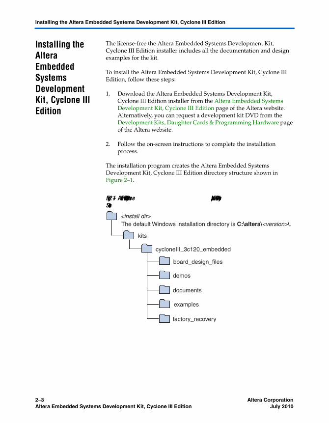
The installation program creates the Altera Embedded Systems Development Kit, Cyclone III Edition directory structure shown in Figure 2–1.
Figure 2–1. Altera Embedded Systems Development Kit Installed Directory Structure
<install dir>
documents
board_design_files
The default Windows installation directory is C:\altera\<version>\.
examples
factory_recovery
demos
kits
cycloneIII_3c120_embedded
2–3 Development Board Version 1.0. Altera CorporationAltera Embedded Systems Development Kit, Cyclone III Edition July 2010

Software Installation
Table 2–1 lists the file directory names and a description of their contents.
Licensing IP Shipping Vs. OpenCore Plus IP Licensing
On purchase of any IP you will have access to shipping license for an IP allowing you to ship the IP in your end product. However if you would like to evaluate IP before purchase then you can do so using the OpenCore Plus version of the IP. Any designs you create operate in Altera’s OpenCore Plus evaluation mode and allow you to perform the following tasks:
1. Simulate the behavior of the Nios II processor IP within your system.
2. Verify the functionality of your design, as well as evaluate its size and speed quickly and easily.
3. Generate time-limited device programming files for designs that include a Nios II processor.
4. Program a device and verify your design in hardware.
OpenCore Plus hardware evaluation supports the following two modes of operation:
Tethered—requires a JTAG connection between your board and the host computer. If tethered mode is supported by all Mega-Cores in a design, the device can operate for a longer time or indefinitely.
Untethered—the design runs for a limited time.
Table 2–1. Installed Directory Contents
Directory Name Description of Contents
Board_design_files Contains schematic, layout, assembly and bill of materials for each of the boards in the kit.
Documents Contains the kit documentation including reference manuals, user guides as well as hardware and software tutorials
Examples Contains design examples which comprise of example processor systems and example software applications
Demos Contains ready-to-run SD Card demos and other design example primarily for demonstration purposes only
Factory_recovery Contains files required to restore the original Flash contents of the board.
Altera Corporation Development Board Version 1.0.2–4July 2010 Altera Embedded Systems Development Kit, Cyclone III Edition
Licensing IP
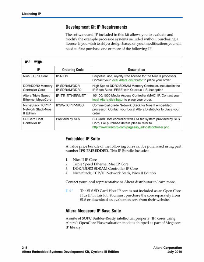
Development Kit IP Requirements
The software and IP included in this kit allows you to evaluate and modify the example processor systems included without purchasing a license. If you wish to ship a design based on your modifications you will need to first purchase one or more of the following IP:
Embedded IP Suite
A value price bundle of the following cores can be purchased using part number IPS-EMBEDDED. This IP Bundle Includes:
1. Nios II IP Core2. Triple Speed Ethernet Mac IP Core3. DDR/DDR2 SDRAM Controller IP Core4. NicheStack, TCP/IP Network Stack, Nios II Edition
Contact your local representative or Altera distributor to learn more.
1 The SLS SD Card Host IP core is not included as an Open Core Plus IP in this kit. You must purchase the core separately from SLS or download an evaluation core from their website.
Altera Megacore IP Base Suite
A suite of SOPC Builder-Ready intellectual property (IP) cores using Altera’s OpenCore Plus evaluation mode is shipped as part of Megacore IP library:
Table 2–2. IP Ordering Information
IP Ordering Code Description
Nios II CPU Core IP-NIOS Perpetual use, royalty-free license for the Nios II processor. Contact your local Altera distributor to place your order.
DDR/DDR2 Memory Controller Core
IP-SDRAM/DDRIP-SDRAM/DDR2
High Speed DDR2 SDRAM Memory Controller, included in the IP Base Suite -FREE with Quartus II Subscription
Altera Triple Speed Ethernet MegaCore
IP-TRIETHERNET 10/100/1000 Media Access Controller (MAC) IP. Contact your local Altera distributor to place your order.
NicheStack TCP/IP Network Stack-Nios II Edition
IPSW-TCPIP-NIOS Commercial grade Network Stack for Nios II embedded processor. Contact your Local Altera Distributor to place your order
SD Card Host Controller IP
Provided by SLS SD Card Host controller with FAT file system provided by SLS Corp, For purchase details please refer to http://www.slscorp.com/pages/ip_sdhostcontroller.php
2–5 Development Board Version 1.0. Altera CorporationAltera Embedded Systems Development Kit, Cyclone III Edition July 2010

Software Installation
■ Finite Impulse Response (FIR) Compiler■ Fast Fourier Transform (FFT) Compiler■ Numerically Controlled Oscillator (NCO) Compiler■ DDR SDRAM Controller■ DDR SDRAM High-Performance Controller■ DDR2 SDRAM Controller■ DDR2 SDRAM High-Performance Controller■ DDR3 SDRAM High-Performance Controller■ QDRII SRAM Controller■ RLDRAM II Controller■ SerialLite II
To help shorten your design time, Altera provides some of its most popular intellectual property (IP) cores with the Altera® IP Base Suite, which is completely free with a Quartus® II subscription.
Registering IP licenses
To register IP licenses simply follow the instructions below:
1. Go to Altera website www.altera.com/licensing.
2. Click on IP licensing for Development Kits link.
3. Follow the on-line instructions to request your license. You will need to enter the serial number of the kit as well as the NIC ID for the PC on which the licenses are to be installed.
4. A license file is e-mailed to you. Save this file on your computer.
Purchasing Software tools and Operating systems
As part of the Nios II Embedded Development Suite (EDS), evaluation versions of Nios II C to Hardware (C2H) compiler, NicheStack TCP/IP Network Stack, Nios II Edition and Micrium’s MicroC/OS II real time operating system (RTOS) are also available.
Nios II C2H Compiler
You can create, compile, and generate time-limited Nios II processor systems and hardware accelerators generated by the Nios II C2H Compiler without obtaining a license file by using the OpenCore Plus evaluation feature. You must obtain a license for the Nios II processor core (ordering code: IP-NIOS) and Nios II C2H Compiler (ordering code: IPT-C2H-NIOS) to generate non-time-limited programming files and flash programming files. Contact your local Altera representative or use the Altera Tools Support to order today. You do not need a license if you will only be developing software using the Nios II IDE.
Altera Corporation Development Board Version 1.0.2–6July 2010 Altera Embedded Systems Development Kit, Cyclone III Edition

Purchasing Software tools and Operating systems
Micrium MicroC/OS-II RTOS
You can develop software for any of the Nios II development kits using the Micrium MicroC/OS-II RTOS. To generate software to run on other boards and/or ship in a product, you must obtain a license. To obtain a license for the Micrium MicroC/OS-II RTOS, contact Micrium today.
NicheStack TCP/IP Network Stack, Nios II Edition
NicheStack TCP/IP Network Stack - Nios II Edition is a software suite of networking protocols designed from the ground up to provide an optimal solution for designing network-connected embedded devices with the Nios II processor.
InterNiche Technologies and Altera collaborated to provide a version of InterNiche’s NicheStack IPv4 network stack optimized for the Nios II architecture. The stack has a small footprint, is portable, and delivers high performance without compromising compliance to RFC standards. NicheStack supports a wide variety of physical interfaces, and can be configured as a standard client machine, an Internet protocol router (IPv4), or a multi-homed server. The suite also contains a comprehensive device networking package, FTP, Telnet, IGMPv1, and DNS and DHCP client components.
The NicheStack TCP/IP Network Stack - Nios II Edition is distributed by Altera as full ANSI C source code and includes an evaluation license. If you wish to design with this software suite, you must purchase a license from Altera (ordering code IPSW-TCPIP-NIOS).
2–7 Development Board Version 1.0. Altera CorporationAltera Embedded Systems Development Kit, Cyclone III Edition July 2010

Software Installation
Altera Corporation Development Board Version 1.0.2–8July 2010 Altera Embedded Systems Development Kit, Cyclone III Edition
Altera Corporation July 2010 PreliminaryA
3. Development Board Setup
Instructions The instructions in this section explain how to install the development board and run the ready-to-run applications using the LCD Color Touch Panel.
Requirements If not already installed, you should:
1. Install the Quartus II Web Edition software on the host computer. For more information, refer to “Installing the Quartus II Web Edition Software ” on page 2–1.
2. Install the Altera Embedded Systems Development Kit, Cyclone III Edition. For more information, refer to “Installing the Altera Embedded Systems Development Kit, Cyclone III Edition ” on page 2–3.
3. Install the USB-Blaster driver software on the host computer. The Cyclone III FPGA development board includes integrated USB-Blaster circuitry so no USB-Blaster module is required for this board.
1 The USB-Blaster driver software is provided with the Quartus II software installation. Communication between the host computer and the development board requires that the USB-Blaster driver software be set up.
Powering Up the Board
To power up the development board, perform the following steps:
Ensure that only the LCD Multimedia HSMC is connected to HSMC Port B of the Cyclone III FPGA development board.
1. Ensure that the POWER switch (SW2) on the Cyclone III FPGA development board is in the OFF (or UP) position.
2. Connect the 16 V DC adapter to the development board and to a power source.
c Only use the supplied 16 V power supply. Power regulation circuitry on the board could be damaged by supplies greater than 16 V.
Development Board Version 1.0. 3–1ltera Embedded Systems Development Kit, Cyclone III Edition

Development Board Setup
3. Slide the POWER switch to ON. The nearby blue POWER light-emitting diode (LED) lights up. Confirm that the user LEDs 0-7 light up.
4. A Welcome screen displays as shown in Figure 3–1.
Figure 3–1. Welcome Screen
Run the Application Selector
The Application selector is the factory system design which boots up on power-on and allows users to quickly select, load, and run different Ready-to-Run applications stored on an SD Card using the LCD touch panel.
There are a couple of ways the application selector can update your board
1. In system update via the on board SD Card: This is where applications are stored in the system, in this case on the SD Card and updated by updating the Flash and reconfiguring the FPGA device
2. Remote-System Update via Ethernet: This is where applications are stored on your local PC or any remote location and downloaded to the Flash via an Ethernet Link to the board.
In order to run the application selector and load and view demos stored on the SD Card (in-system update) follow the instructions below:
Altera Corporation Development Board Version 1.0.3–2July 2010 Altera Embedded Systems Development Kit, Cyclone III Edition

In system update via SD Card: How it works
1. Connect power to the development board, and turn on the power switch. You should see the application selector begin to start up on your LCD panel.
1 If the application selector does not start when power is applied or when the board is reset, see the Chapter 11, Restoring the Factory Design to the Flash Device.
2. Touch the application to highlight your selected application
1 If there are more than five applications on the SD Card, you can scroll through the list by touching the scroll-up and scroll-down buttons on the right hand side of the screen.
3. To get more information about a particular application, highlight the application by touching it and then touching the button labeled Show Info.
1 If there is additional information available for the application you highlighted, a scrollable text window will appear. To return to the main menu, touch the button labeled OK.
4. When you’ve selected the application you want to load, touch the button labeled Load.
1 The application will begin loading, and a small window will be displayed showing the progress. Loading can take up to a few minutes, depending on the size of the application, and whether it was previously cached in on-board flash memory.
In system update via SD Card: How it works
A ready-to-run application consists of a FPGA hardware image and an application software image. The application selector will boot from flash, and a splash screen will appear while the application selector searches for applications on the SD Card. When the main menu appears, you will see a scrollable list of applications. These are the applications which were found on the SD Card and are now available to load. When you load an application the application selector copies these images from the SD Card to the Flash memory and reconfigures the FPGA with your selection. For more information, refer to Chapter 5, Ready-to-Run Applications.
For more detailed information about the Application Selector Utility, refer to Chapter 8, Application Selector Details.
3–3 Development Board Version 1.0. Altera CorporationAltera Embedded Systems Development Kit, Cyclone III Edition July 2010
Development Board Setup
Get the latest Ready-to-Run Demos
New ready-to-run demos and design examples can be found in the Altera Embedded Systems Development kit, Cyclone III Edition page.
You can download the demos and add them to your SD card. For instructions on how to update your SD Card with the latest designs, refer to Chapter 5, Ready-to-Run Applications.
Add your own applications from the LCD touch panel using the Application Selector
You can easily convert your own designs into ready-to-run applications so that they can be loaded via the LCD Color Touch Panel by the Application Selector. For information on how to create your own ready-to-run applications refer to Chapter 5, Ready-to-Run Applications.
Programming Flash with Custom FPGA Configuration
c Programming the Flash with a new FPGA configuration will overwrite default application selector factory design. You will lose all access to the ready-to-run demos on the LCD screen.
To program the flash device on the development board, you must have first created an SRAM Object File (SOF) first. To download a SOF configuration bit stream into the flash device, perform the following steps:
1. Ensure that the Power switch SW2 is in the OFF (or DOWN) position.
2. Connect the USB Cable to the USB port on the board
3. Cycle the POWER switch OFF then ON.
4. From the Quartus II menu, choose Tools > Programmer.
5. Click Auto Detect. The EP3C120 device appears on the list of devices to be programmed.
6. Double-click the File ><none> field. This opens a Select New Programming File window.
7. Choose the desired SOF and click Open.
8. Select the Program/Configure check-box
Altera Corporation Development Board Version 1.0.3–4July 2010 Altera Embedded Systems Development Kit, Cyclone III Edition

Restoring the Factory Design to the Flash device
9. Click Start to download the selected configuration file to FPGA. When the progress bar reaches 100% the FPGA is ready to access and program the Flash device
You have now successfully programmed the flash device with a configuration for your board. To configure the board form the flash device, power cycle the board. Powering on the board causes the flash device to load a new configuration into the FPGA. The CONF DONE LED lights up and the hardware functions associated with the design take effect.
Restoring the Factory Design to the Flash device
To restore the development board to factory conditions, refer to instructions as described in Chapter 11, Restoring the Factory Design to the Flash Device.
3–5 Development Board Version 1.0. Altera CorporationAltera Embedded Systems Development Kit, Cyclone III Edition July 2010
Development Board Setup
Altera Corporation Development Board Version 1.0.3–6July 2010 Altera Embedded Systems Development Kit, Cyclone III Edition
Altera Corporation July 2010 PreliminaryA
4. Remote System Update ViaEthernet
There are two ways you can update your board with a new design. The first, as described in the previous chapter is In system update, where designs are stored on the SD Card and programmed to flash. In this chapter, we will discuss the second method; Remote system udpate. In remote system update, designs are stored remotely on your PC and transferred to flash via Ethernet.
1 Please note that the files that you will download via Ethernet are not the same as those you will download via the SD Card. However both start with a standard FPGA hardware image (.SOF) file and optionally a standard software executable (.ELF). The provided scripts will allow you to take any design and convert it to the format needed to download via Ethernet.
About Remote System Update
Imagine you are working at your desk and your system is physically located elsewhere (such as in the lab or manufacturing facility). Having remote system update capability in your FPGA allows you to update your kit with new designs so long as there is a persistent Ethernet connection.
If a new design becomes available for the Altera Embedded Systems Development Kit, Cyclone III edition you can download it to your local computer and then use the remote system update capability to update your kit with the new design by programming it to flash via Ethernet.
Remote System Update: How it works
Remote system update is another capability of the Application Selector.
■ When your kit is connected to a network, it serves up a web page. The content referred to as Board Update Portal are stored in the SD Card in a folder entitled webserver_html.
■ From any computer, you can view the Board Update Portal by simply typing the correct IP address on a web browser.
■ By following the instructions displayed on the web page you can browse to and load a design stored on the local computer and program it to the flash on your board.
■ You can then reset the FPGA on your board and the FPGA should reconfigure from the newly programmed Flash image.
Development Board Version 1.0. 4–1ltera Embedded Systems Development Kit, Cyclone III Edition

Remote System Update Via Ethernet
Requirements
All designs to be downloaded to flash should be available on our local computer. You will need
1. A local computer with a connection to a working Ethernet port.
2. A separate working Ethernet port to connect to your board.
3. Flash files for hardware and software images to update the board with. These must be present on your local computer. For the sake of simplicity an example set of flash files has been provided in your the altera/<version #>/kits/ cycloneIII_3C120_embedded/ examples/ application_selector/remote_system_update folder.
1 The .flash file format is an SREC file with addressing offset from the base address of your flash device. For information on how to create the necessary flash files from your design refer to “Creating Flash Files for Remote System update ”
Operating Instructions for Remote System Update
1. Apply power to the board by plugging in the power cable and pressing switch SW1
1 The application selector will appear on the LCD Screen. On the bottom right you will see a button that should say “Not Connected”. You may click on the button to view the instructions for remote system update and click OK to return to the main screen.
2. Using an Ethernet cable, connect the Ethernet RJ-45 jack on the LCD Multimedia HSMC to a working Ethernet port.
1 The connection to Ethernet port will be detected by the application which will try to acquire a suitable IP address. During this time you will see the message “Connecting…” on the LCD screen.
3. Please wait while the web server application establishes a connection to the internet and acquires an IP Address via DHCP. On completion the IP Address will be displayed on the LCD Screen.
4. On your host PC ensure that it is connected to another working Ethernet port and open a web browser.
5. In the web browser, type the IP address displayed on the LCD screen (e.g. 168.57.231.12) and hit Enter
Altera Corporation Development Board Version 1.0.4–2July 2010 Altera Embedded Systems Development Kit, Cyclone III Edition

Creating Flash Files for Remote System update
1 You should now see the Board Update Portal displayed on the web browser which is a set of web pages served up by the board from the contents of the webserver_html directory on the SD Card.
6. On the upper left hand side on the web form, click on the link under Read the instructions. You will be directed to the remote configuration instruction page. Carefully read the instructions for remote configuration.
7. Click on the Left hand side of the web page you will see a CFI Flash Upload section. Click Browse buttons and browse to the hardware and (optionally) software Flash image on your PC and click Open. Browse to the software flash images on your PC and click Open.
1 Example files are available in your Dev Kit installation at:
altera/<version #>/examples/ application_selector/ application_utilities/remote_system_update/C2H_Mandelbrot_hw.flash
8. On the web page click Upload.
1 Upon completion you will be directed to a form entitled Reset System
9. Click on the Reset System button. The FPGA should now reconfigure from the newly programmed contents of the Flash file.
10. Please wait while the hardware Flash image is uploaded to your board. When this is done you will be directed to another web form entitled Program CFI Flash.
Creating Flash Files for Remote System update
The image required for remote system update consists of a Flash image for FPGA configuration and if your system has a software application then a Flash image for the software application. To create the flash files you must have
■ The Nios II EDS and Quartus II FPGA design software installed on your PC.
■ A hardware SRAM object file (*.SOF) must have the cpu reset address configured from the Flash device at offset 0x0.
■ An Executable Link Format file (ELF) which is the result of the software compilation process.
4–3 Development Board Version 1.0. Altera CorporationAltera Embedded Systems Development Kit, Cyclone III Edition July 2010
Remote System Update Via Ethernet
■ On your host PC, launch a Nios II Command Shell from Start -> Programs -> Altera -> Nios II <version> EDS -> Nios II Command Shell
■ From the command shell navigate to where your SOF file is located and create your hardware Flash image using the following command:
● sof2flash --compress --input="your SOF.sof" --output="your SOF.flash" --offset=0x3880000.
■ From the command shell navigate to where your ELF file is located and create your software Flash image using the following command:
elf2flash --base=0x10000000 --end=0x013FFFFFF --reset=0x10240000 --input="your ELF.elf" --boot=$SOPC_KIT_NIOS2/components/altera_nios2/boot_loader_cfi.srec
If you need to update more images (hardware or software) click the main hyperlink (takes you back to the main/index page) and repeat step 1-3 as necessary.
Altera Corporation Development Board Version 1.0.4–4July 2010 Altera Embedded Systems Development Kit, Cyclone III Edition

Altera Corporation July 2010 PreliminaryA
5. Ready-to-Run Applications
About Ready-to-Run applications
Ready-to-Run demo applications provide a quick and easy way to evaluate full processor systems built for automotive, industrial and consumer applications. Many of the ready-to-run demos shipped with this kit have been provided by Altera’s partners. You can use the application selector to select and load the demonstration of choice. New demos or applications that you have created can be easily made "ready-to-run" for quick select and load via the LCD Color Touch Panel.
Ready-to-Run demo applications are provided in binary format only (.FLASH). Full Quartus II projects, source code, IP licensing etc. can be obtained by contacting the provider of the Ready-to-Run demo. You will find these demos on your SD Card, but new Ready-to-Run demos can also be downloaded from www.altera.com/esdk. Simply download the demo from the above web-site and copy it to your SD Card. For details see the section “How to update your SD Card with Ready-to-Run Applications” on page 5–2.
The partial list of Ready-to-Run demonstration applications is shown in the table below.
Table 5–1. Demonstration Application Description
Name of Ready-to-Run Demo Vendor Description
Altera Mandelbrot C2H Altera Demonstrates the performance advantage of implementing compute intensive C language based algorithm in hardware (HDL). Hardware acceleration demonstrated here uses the Nios II C2H Compiler “Right click to Accelerate” technology.
DAVE 2D Graphics Demo TES Demonstrates powerful 2D vector graphics capabilities of DAVE 2D Engine including sub-pixel accuracy, anti-aliasing, alpha blending, bit-blitting and 2.5 D imaging
Photo Frame by PlanetWeb PlanetWeb This Nios II based Digital Photo Frame Application from Planetweb lets you takes pictures and displays on the LCD color touch panel in slide show, thumb nail and other modes
Development Board Version 1.0. 5–1ltera Embedded Systems Development Kit, Cyclone III Edition
Ready-to-Run Applications
1 Please visit www.altera.com/esdk to contact the vendors and request more information. These demos have been provided as flash files and not full Quartus II Projects.
Where to get the latest Ready-to-Run SD Card Demo Applications
In addition to the pre-packaged Ready-to-Run SD Card Demo applications which come with the Altera Embedded Systems Development Kit, Cyclone III Edition, more are available from Altera or through third party vendors.
To get more Ready-to-Run SD Card demo applications visit:
www.altera.com/esdk
Also, you can easily convert your own applications to be loadable by the application selector “Creating your own Ready-to-Run Applications” on page 5–5
How to update your SD Card with Ready-to-Run Applications
The following instructions will explain how you can update your SD Card with ready-to-run demos:
■ Make sure your ready-to-run demo is on your local PC■ Remove the SD Card from your development kit and connect to your
local PC using the provided SD to USB card adapter■ Copy the ready-to-run demo to your SD Card directory under the
folder altera_3C120_apps.■ Connect the SD Card back to SD connector slot on the LCD
Multimedia HSMC■ Apply power to the development kit■ On boot up the Application Selector should be able to find the ready-
to-run demo and display it on the LCD screen■ Touch to highlight and press Load to load the new demo
SpectraWorks GUI demo by PlanetWeb
PlanetWeb Demonstrates the high quality graphics, text and instant re-branding capabilities of PlanetWeb Spectra Core Graphics IP. The PlanetWeb graphics were created by SpectraWorks GUI Builder
Menudemo by PlanetWeb PlanetWeb Demonstrates the high quality menu rendering and instant re-branding capabilities of PlanetWeb Spectra Core Graphics IP. The PlanetWeb graphics were created by SpectraWorks GUI Builder
Table 5–1. Demonstration Application Description
Name of Ready-to-Run Demo Vendor Description
Altera Corporation Development Board Version 1.0.5–2July 2010 Altera Embedded Systems Development Kit, Cyclone III Edition

Where to find the Ready-to-Run demos on the SD Card
Where to find the Ready-to-Run demos on the SD Card
In addition to the SD Card the ready-to-run demos are also located in the <installation_dir>/demos/sdcard_contents directory.
What’s in your SD Card?
If you plug your SD Card to your host PC using the provided SD to USB adapter you will see a directory structure. In these directories are where the Application selector finds and displays the various ready-to-run demos.
Below is an example of how applications are organized on the SD Card.
Figure 5–1. SD Card Directory Structure
Table 5–2 lists the SD Card Directory structure description.
Table 5–2. SD Card Directory Structure Description
SD Card Folder Description
Altera_3C120_apps All ready-to-run applications and demos are stored in this directory. In the following section you will learn what constitutes a ready-to-run applications.
Image Photos and JPEG images are stored here. These are read by the Planetweb Digital Photo Frame application, so if you put your favorite JPEGS here they will get displayed by the Digital Photo Frame
Webserver_html When the Ethernet port on the LCD HSMC is connected to the network an IP address is displayed and a web page is served up from your kit. This folder stores the static web pages that get served up (by the application selector)
5–3 Development Board Version 1.0. Altera CorporationAltera Embedded Systems Development Kit, Cyclone III Edition July 2010

Ready-to-Run Applications
What’s in a Ready-to-Run Application?
This section describes some details about the 3 components that make up a ready-to-run Application,
■ All loadable applications on the SD Card must be located in a top-level directory named altera_3C120_apps.
■ Under the altera_3C120_apps directory, each application is located in its own subdirectory. The name of that subdirectory is important because the application selector utility uses that name as the title of the application when displaying it in the main menu. The name of the subdirectory is the title that will be displayed for your application in the menu. The subdirectory names can be anything so long as they adhere to the FAT file system long file name rules. Spaces are permitted.
■ The SD Card must be formatted with the FAT 16 file system, and can be any capacity up to 2GB. Long file names are supported.
■ Each loadable application consists of two flash files, and an optional text file, all stored on an SD Card.
Table 5–3. Ready-to-Run Application Components Description
Ready-to-Run Application Components Description
<filename>_sw.flash The FLASH file that contains the software portion of the application. It is derived from an .ELF file as described in the section of this document titled “Creating your own Ready-to-Run Applications”. This flash file can be named anything supported by the FAT16 file system, the only restriction being that the name must end with _sw.flash
<filename>_hw.flash Flash file represents the hardware portion of the application. It is derived from a .SOF file as described in the section of this document titled “Creating your own Ready-to-Run Applications”. This file can be named anything supported by the FAT 16 file system, the only restriction being that the name must end with _hw.flash
Info.txt The optional info.txt file contains additional information about the application. In the application selector utility, touching the Show Info button while your application is highlighted, brings up a window showing the text contained in this file. The name of this text file must be info.txt, or the application selector will not recognize it.
Altera Corporation Development Board Version 1.0.5–4July 2010 Altera Embedded Systems Development Kit, Cyclone III Edition
Creating your own Ready-to-Run Applications
Creating your own Ready-to-Run Applications
Designs that you create can also be made selectable by the application selector i.e. made into a ready-to-run application. To create a ready-to-run application from your design you will need:
■ A hardware image (SRAM Object File or SOF)■ A software image which runs on that hardware (an Executable and
Linkable format file or .ELF file). 1 This .ELF file is not required if your demo is hardware only
and has no software application associated with it.
■ The only restrictions are: a. The .SOF file must contain a CFI flash component.
b. The .SOF file must contain a Nios II CPU whose reset address is set to CFI Flash at offset 0x00000000.
c. The size of the software image must be no larger than 20 MBytes.
1. Once you have your working .SOF and .ELF file pair, perform the following steps to convert them to a loadable application selector-compatible application.
2. Copy both the .SOF and .ELF files into a common directory of your choosing. This directory is where you will convert the files.
3. Copy the script entitled n2c3.sh located in your development kit in the <install_dir>/: examples/application_selector/application_utilities/ flash_file_conversion_script folderto the directory where you copied your .SOF and .ELF files. Optionally, copy it to a directory in the Nios II Command Shell search path i.e. <nios2 install>/bin
4. From Start menu, select All Programs, Altera, Nios II EDS, Nios II <version> Command Shell to open the Nios II Command Shell and and change to the directory where you copied the .SOF and .ELF files.
5. In the Nios II Command Shell type the command ./n2c3.sh <elf_file>.elf <sof_file>.sof
The n2c3.sh script runs the Nios II Command Line utilities sof2flash and elf2flash to convert the .SOF and .ELF files to application selector-compatible .FLASH files.
5–5 Development Board Version 1.0. Altera CorporationAltera Embedded Systems Development Kit, Cyclone III Edition July 2010

Ready-to-Run Applications
1 Feel free to open n2c3.sh in a text editor to see the exact commands which are run.
6. You will now see two new files in the directory, <elf file>_sw.flash, and <sof file>_hw.flash. These are the application files you will put on the SD Card.
7. Now create a file named info.txt in the same directory.
This is the file which will be displayed in the Application Selector when the Show Info button is pressed for your application. Fill info.txt with some descriptive text about your application’s operation.
8. Create a new subdirectory and name it what you would like the title of your application to be shown as in the application selector.
9. Copy both .flash files and info.txt into the new directory.
10. Using an SD Card reader, copy the directory onto an SD Card into a directory named altera_3C120_apps. The directory structure on the SD Card should look as shown in the Figure 5–1above.
11. Place the SD Card in the Altera Embedded Systems Development Kit, Cyclone III Edition board, and switch on the power. The Application Selector will start up, and you will now see your application appear as one of the selections.
Altera Corporation Development Board Version 1.0.5–6July 2010 Altera Embedded Systems Development Kit, Cyclone III Edition
Altera Corporation July 2010 PreliminaryA
6. Example ProcessorSystems
About the Example Processor Systems
Example Processor Systems are Quartus II SOPC Builder designs featuring a processor and peripherals targeted for the Altera Embedded Systems Development Kit, Cyclone III Edition hardware.
Purpose
These pre-generated example processor systems can be used as starting points for your own embedded development.
Examples
There are two example processor systems provided in the kit:
■ Nios II 3C120 General Purpose Microprocessor System (standard)■ Nios II 3C120 Microprocessor System with LCD Controller (lcd)
Where to find
Provided in the altera\<version>\kits\cycloneIII_3C120_embedded\examples folder, under standard and lcd respectively.
Benefits
■ Hardware designers can accelerate their own SOPC Builder system development by using the Nios II 3C120 General Purpose Microprocessor System as a starting point.
■ Since the board boots up with the Nios II 3C120 Microprocessor System with LCD Controller software developers can use it for software development right out of the box.
About the Nios II 3C120 General Purpose Microprocessor System
Within the FPGA is the Nios II 3C120 General Purpose Microprocessor System; a Nios II processor based hardware system that can be used as a starting point for embedded application development.
Location
<install dir>/examples/standard
Development Board Version 1.0. 6–1ltera Embedded Systems Development Kit, Cyclone III Edition
Example Processor Systems
Description
Simple general purpose Nios II-based processor system targeted for the Altera Embedded Systems Development Kit, Cyclone III Edition that includes a CPU, DDR2 Memory controller, timers, PLLS and other peripherals. The processors system can easily be modified using SOPC Builder or added to your existing Quartus II project as a component.
IP licenses required to Ship design
Most of the IP cores used in this design require no licensing. The following IP licenses however are required to ship design:
■ Nios II IP evaluation license with Nios II EDS■ DDR2 SDRAM memory controller core shipping license from Altera
1 For more information on how to obtain evaluation or shipping licenses for the above refer to “Licensing IP” on page 2–4.
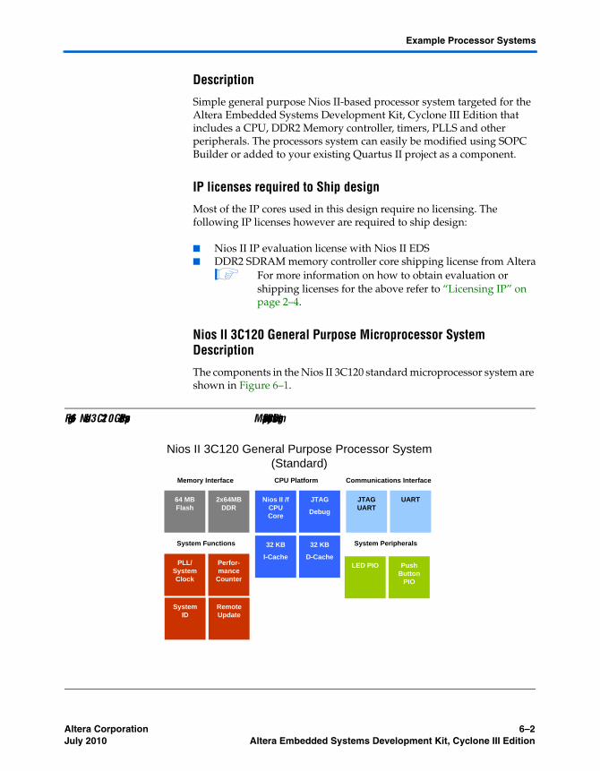
Nios II 3C120 General Purpose Microprocessor System Description
The components in the Nios II 3C120 standard microprocessor system are shown in Figure 6–1.
Figure 6–1. Nios II 3C120 General Purpose Microprocessor Systems Block Diagram
CPU Platform
System Functions
Nios II /f CPU Core
JTAG
Debug
32 KB
I-Cache
32 KB
D-CachePLL/
System Clock
Perfor-mance
Counter
System ID
Remote Update
Memory Interface
2x64MB DDR
64 MB Flash
Communications Interface
JTAG UART
UART
System Peripherals
Push Button
PIO
LED PIO
Nios II 3C120 General Purpose Processor System (Standard)
Altera Corporation Development Board Version 1.0.6–2July 2010 Altera Embedded Systems Development Kit, Cyclone III Edition

About the Nios II 3C120 General Purpose Microprocessor System
CPU Platform
The CPU platform consists of
■ Nios II/f cpu core ■ JTAG Debug Port■ 32KB Instruction Cache■ 32KB Data Cache
Memory Interfaces
■ DDR2 SDRAM Controller● Run time program and data memory
■ CFI Flash Controller ● Stores FPGA configuration data
Communication Interfaces
■ JTAG UART ● Used for Serial communication and debugging Nios II
applications via the on-board USB-Blaster circuitry.
Peripheral Set
■ PLL ● Accepts the global input clock source from the 50MHz on-board
oscillator and generates the following clocks ● 100 MHz CPU Clock ● 60 MHz Peripheral Clock (“slow peripherals”)
■ System Clock Timer ● General purpose system timer.
■ Performance Counter ● Counter used for debug and system performance analysis.
■ System ID ● Used to sync the hardware system generation with the software
generation tools. ■ Max II Interface
● Communicates with the Max II CPLD on the base board. The Max II CPLD manages configuration of the FPGA on boot up using Fast Passive Parallel (FPP) configuration scheme.
■ LED PIO ● Output only control block for LED1-LED4
■ Pushbutton PIO ● Input only control block for the on-board pushbuttons.
■ PIO for ID EEPROM (I2C) ● Used to communicate with the EEPROM ID chip which stores
information about the board
6–3 Development Board Version 1.0. Altera CorporationAltera Embedded Systems Development Kit, Cyclone III Edition July 2010

Example Processor Systems
● 1 The I2C interface is implemented using software and general-purpose I/Os connected to the Standard System
About the Nios II 3C120 Microprocessor System with LCD Controller
Location
<install dir>/examples/lcd
Description
A feature rich general purpose processor system featuring including 32-bit Nios II Processor, 10/100 Ethernet MAC, SD Card controller and LCD Color touch panel control.
IP licenses required to ship design
Most of the IP cores used in this design require no licensing. The following IP licenses however are required to ship design:
■ Nios II CPU IP Core■ DDR2 SDRAM memory controller core■ TSE MAC IP Core■ SD Card controller core shipping license from SLS Corp
Nios II 3C120 Microprocessor System with LCD Controller System Description
Full details about the processor system can be found in Nios II 3C120 Microprocessor System with LCD Controller Data Sheet on www.altera.com/esdk.
Altera Corporation Development Board Version 1.0.6–4July 2010 Altera Embedded Systems Development Kit, Cyclone III Edition
About the Nios II 3C120 Microprocessor System with LCD Controller
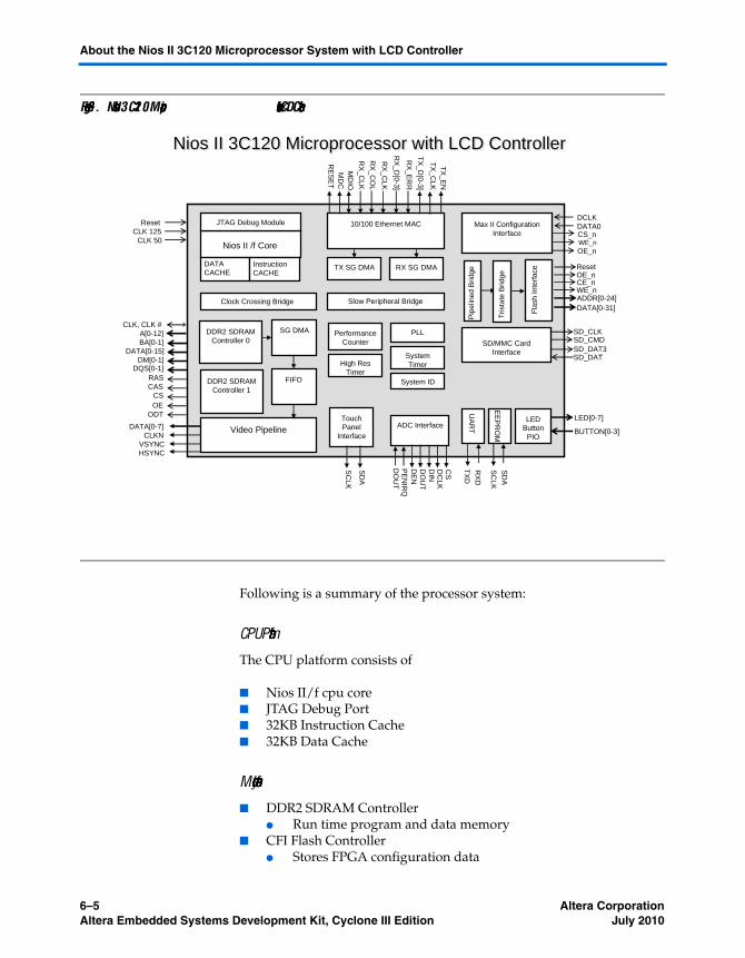
Figure 6–2. Nios II 3C120 Microprocessor with LCD Controller
Following is a summary of the processor system:
CPU Platform
The CPU platform consists of
■ Nios II/f cpu core ■ JTAG Debug Port■ 32KB Instruction Cache■ 32KB Data Cache
Memory Interfaces
■ DDR2 SDRAM Controller● Run time program and data memory
■ CFI Flash Controller ● Stores FPGA configuration data
A[0-12]BA[0-1]
DATA[0-15]DM[0-1]
CASCSOE
ODT
DATA[0-7]CLKN
VSYNCHSYNC
Nios II /f Core
DATA CACHE
JTAG Debug Module
Fla
sh In
terf
ace
SD/MMC Card Interface
PLL
UA
RT
Touch Panel
Interface
LED Button
PIO
Performance Counter
10/100 Ethernet MAC
DDR2 SDRAM Controller 0
SG DMA
FIFO
System TimerHigh Res
TimerSystem ID
TX SG DMA RX SG DMAInstruction CACHE
DDR2 SDRAM Controller 1
Slow Peripheral BridgeClock Crossing Bridge
Max II Configuration Interface
Video Pipeline
ResetCLK 125
CLK 50
DCLKDATA0CS_nWE_nOE_n
CLK, CLK #
DQS[0-1]RAS
OE_n
ADDR[0-24]DATA[0-31]
Reset
CE_nWE_n
ADC Interface
CS
DC
LKD
IND
OU
TD
EN
PE
NIR
QD
OU
T
SD
A
SC
LK
RE
SE
TM
DC
MD
IO
RX
_CLK
RX
_CO
L
RX
_CLK
RX
_D
[0-3]
RX
_ER
R
TX
_D
[0-3]
TX
_C
LKT
X_E
N
SD_CMDSD_CLK
SD_DATSD_DAT3
LED[0-7]
BUTTON[0-3]
RX
D
TX
D
EE
PR
OM
SD
A
SC
LK
Pip
elin
ed B
ridge
Tri
stat
e B
ridg
e
Nios II 3C120 Microprocessor with LCD ControllerNios II 3C120 Microprocessor with LCD Controller
6–5 Development Board Version 1.0. Altera CorporationAltera Embedded Systems Development Kit, Cyclone III Edition July 2010

Example Processor Systems
■ SD Card ● The controller, API, and FAT File System for the SD-Card used
in the Nios II LCD System is provided under license agreement by SLS (http://www.slscorp.com)
● The example processor system contains the SD MMC SPI CORE which is a component that has been provided by a third party vendor, SLS in encrypted format. To compile this core in your SOPC Builder system, you will need to get a license from SLS. However, if your particular application has no need to access the SD Card then you do not need to include the SD Card core in your system. Simply uncheck this core or delete it and re-generate the system. You should now be able to rebuild the hardware system without error.
Communication Interfaces
■ Ethernet MAC● 10/100 Ethernet connection for the Ethernet port on the LCD
Multimedia HSMC■ JTAG UART
● Used for Serial communication and debugging Nios II applications via the on-board USB-Blaster circuitry.
■ UART ● Serial communication link for general purpose communications
and debug.
Peripheral Set
■ PLL ● Accepts the global input clock source from the 50MHz on-board
oscillator and generates the following clocks • 100 MHz CPU Clock • 100 MHz SSRAM Clock • 66.5 MHz DDR SDRAM Clock • 60 MHz Peripheral Clock (“slow peripherals”) • 40 MHz Remote System Update Clock
■ System Clock Timer ● General purpose system timer.
■ Performance Counter ● Counter used for debug and system performance analysis.
■ System ID ● Used to sync the hardware system generation with the software
generation tools. ■ Max II Interface
● Communicates with the Max II CPLD on the base board. The Max II CPLD manages configuration of the FPGA on boot up using Fast Passive Parallel (FPP) configuration scheme.
Altera Corporation Development Board Version 1.0.6–6July 2010 Altera Embedded Systems Development Kit, Cyclone III Edition
About the Nios II 3C120 Microprocessor System with LCD Controller
■ LED PIO ● Output only control block for LED1-LED4
■ Pushbutton PIO ● Input only control block for the on-board pushbuttons.
■ PIO for ID EEPROM (I2C) ● Used to communicate with the EEPROM ID chip which stores
information about the board 1 The I2C interface is implemented using software and general-purpose I/Os connected to the Standard System
Video Pipeline
The video pipeline outputs the appropriate pixel data and sync signals to the LCD Touch Panel. It provides high bandwidth memory access that allows for flicker free display on the color LCD. The video pipeline is comprised of:
■ PIO for LCD I2C controller ● The I2C pins are used to configure the LCD panel for brightness
and set the gamma correction curves. ■ SPI touch panel controller
● Used to communicate with the touch panel ADCs. ■ Pixel Converter
● Logic block that converts parallel 32-bit R-G-B-0 data to an 8-bit data stream. This is required because of the pin-limitation placed on the system by the HSMC connector. The video data-stream is multiplexed in the FPGA on the Cyclone III Starter Board and de-multiplexed in the MAX II device on the LCD Multimedia HSMC.
■ Sync Generator ● Generates the horizontal and vertical sync signals for each frame
displayed on the LCD touch screen. ● For more information on the video pipeline (pixel converter and
Video Sync Generator) and GPIO components refer to the Embedded Peripherals IP User Guide.
6–7 Development Board Version 1.0. Altera CorporationAltera Embedded Systems Development Kit, Cyclone III Edition July 2010
Example Processor Systems
Altera Corporation Development Board Version 1.0.6–8July 2010 Altera Embedded Systems Development Kit, Cyclone III Edition

Altera Corporation July 2010 PreliminaryA
7. Example SoftwareApplications
About the Software Applications
Software developers can use the provided software applications to see examples of software drivers for the various hardware peripherals on the Altera Embedded Systems Development Kit, Cyclone III Edition. The kit contains several system designs:
■ Altera Application Selector with Embedded Web Server1 You can locate the system designs in the
altera\<version>\kits\cycloneIII_3C120_embedded\ folder in examples directory. You will also find more system designs from www.altera.com/esdk
About the Application Selector
The application selector is the default utility that boots up on power up. This software application runs on the Nios II 3C120 Microprocessor System with LCD Controller.
Based on processor system
Nios II 3C120 Microprocessor System LCD Controller
Location
<install dir>/examples/application_selector
Description
LCD Color Touch Panel controller, Ethernet controller and SD Card controller based processor system for LCD Color touch panel control, in-system update using SD Card, remote system update using Ethernet.
The application selector illustrates several aspects of software development:
■ Interfacing to the LCD touch panel■ Interfacing to the SD Card using the FAT file system■ Implementing a HTTP web server application using the sockets
interface of NicheStack TCP/IP Network Stack, Nios II Edition■ Implementing remote system update over Ethernet■ Managing multiple FPGA configurations from Flash■ Using the MicroC/OS-II real time operating system
Development Board Version 1.0. 7–1ltera Embedded Systems Development Kit, Cyclone III Edition
Example Software Applications
IP licenses required to ship design
■ SD/MMC SPI Core IP (with FAT file system) from SLS ■ Triple Speed Ethernet-MAC Core license from Altera (Ordering code
IP-TRIETHERNET)■ Nios II CPU IP (Ordering Code IP-NIOS)■ DDR2 SDRAM memory controller core (Part of IP Suite included
with Quartus II Subscription)
c The example processor system contains the SD Host Controller Core which is a component that has been provided by a third party vendor, SLS in encrypted format. To compile this core in your SOPC Builder system, you will need to get a license from SLS. However, if your particular application has no need to access the SD Card then you do not need to include the SD Host Controller core in your system. Simply uncheck this core or delete it and re-generate the system. You should now be able to rebuild the hardware system without error.
Software and middleware licenses required to ship design
■ NicheStack TCP/IP Network Stack, Nios II Edition free evaluation license available with Nios II EDS, shipping license from Altera (Ordering Code IPSW-TCP/IP-NIOS)
■ MicroC/OS-II real time operating system free evaluation license available with Nios II EDS, shipping license to be purchased from Micrium
1 For more information on how to obtain evaluation or shipping licenses for the above refer to “Licensing IP” on page 2–4.
Altera Corporation Development Board Version 1.0.7–2July 2010 Altera Embedded Systems Development Kit, Cyclone III Edition
Altera Corporation July 2010 PreliminaryA
8. Application SelectorDetails
This section describes how to rebuild the Application Selector utility from source code using the Nios II Software Build Tools. If you are new to developing software on the Nios II processor it is recommended that you first go through the tutorial My First Nios II Software Tutorial. This will walk you through compiling a simple project that runs on the Nios.
The Application Selector uses the on-board CFI flash to store several different things. Table 8–1 shows a map of how the different sections of flash are used by the Application Selector.
Hardware Images
CFI flash is used to store both the hardware image of the Application Selector itself, as well as up to 10 hardware images of applications which are being loaded.
The Application Selector hardware image is permanently stored in flash at offset 0x2000000.
Hardware images for the applications being loaded get written to flash at load time to an offset between 0x2380000 and 0x3C00000, depending on caching. Hardware image caching is described in more detail in the section titled “Hardware Image Caching ”.
Software Images CFI flash is used to store the software images of both the Application Selector utility itself as well as software images of applications being loaded. All software images used by the application selector contain a boot copier which is pre-pended by the elf2flash utility during file conversion process described in the “Creating your own Ready-to-Run Applications” on page 5–5” section. The boot copier copies the software code to program memory before running it.
CFI Flash The Application Selector software image is permanently stored in flash at offset 0x100000 Software images for the applications being loaded get written to flash at load time to offset 0x0240000. Software images must be smaller than approx 24MB, or they will overwrite the reserved flash space located at offset 0x1C00000.
Development Board Version 1.0. 8–1ltera Embedded Systems Development Kit, Cyclone III Edition
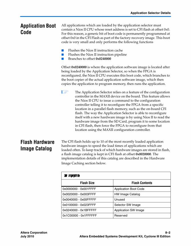
Application Selector Details
Application Boot Code
All applications which are loaded by the application selector must contain a Nios II CPU whose reset address is set to CFI flash at offset 0x0. For this reason, a generic bit of boot code is permanently programmed at offset 0x0 in the CFI Flash as part of the factory recovery image. This boot code is very small and only performs the following functions
■ Flushes the Nios II instruction cache ■ Flushes the Nios II instruction pipeline ■ Branches to offset 0x0240000
Offset 0x0240000 is where the application software image is located after being loaded by the Application Selector, so when the FPGA is reconfigured, the Nios II CPU executes this boot code, which branches to the boot copier of the actual application software image, which then copies the application to program memory, then runs the application.
1 The Application Selector relies on a feature of the configuration controller in the MAXII device on the board. This feature allows the Nios II CPU to issue a command to the configuration controller telling it to reconfigure the FPGA from a specific location in a parallel flash memory, such as the on-board CFI flash. The way the Application Selector is able to reconfigure itself with a new hardware image is by using Nios II to read the hardware image from the SD Card, program it to some location in CFI flash, then force the FPGA to reconfigure from that location using the MAXII configuration controller.
Flash Hardware Image Catalog
The CFI flash holds up to 10 of the most recently loaded application hardware images to speed the load times of applications which are loaded often. To keep track of which hardware images are stored in flash, a flash image catalog is kept in CFI flash at offset 0x0020000. The implementation details of this catalog are described in the Hardware Image Caching section below.
Table 8–1. Memory Map of CFI Flash
Flash Size Flash Contents
0x0000000 - 0x001FFFF Application Boot Code
0x0020000 - 0x003FFFF HW Image Catalog
0x0040000 - 0x00FFFFF Unused
0x0100000 - 0x023FFFF Selector SW Image
0x0240000 - 0x1BFFFFF Application SW Image
0x1C00000 - 0x1FFFFFF Reserved
Altera Corporation Development Board Version 1.0.8–2July 2010 Altera Embedded Systems Development Kit, Cyclone III Edition

Hardware Image Caching
Hardware Image Caching
Copying data from the SD Card to flash is slow due to both the read speed from the SD Card and the write speed of the CFI flash. However the remote update feature allows us to reconfigure the FPGA from anywhere in flash, so we can benefit by persistently holding (caching) a certain number of frequently used application hardware images in flash to avoid having to copy them from the SD Card every time the application is loaded.
The Application Selector utility can cache up to 10 application hardware images in CFI flash. When the user chooses an application to load from the SD Card using the Application Selector, the Application Selector first scans through its catalog of hardware images currently stored in CFI flash to see if any of them match the hardware image being requested. If one of the images cached in CFI flash does match, the Application Selector reconfigures from the offset of that cached hardware image instead of copying the image from SD Card to flash. This significantly reduces the load time.
Caching the hardware images requires the application selector to be able to quickly tell if an image in CFI flash is the same as one on the SD Card. To determine whether a hardware image in flash matches a hardware image on the SD Card, a 32-bit timestamp value is used as a tag. During the file conversion process, the sof2flash utility inserts a 32-bit timestamp in the hardware image .flash file as an S0-type record on the first line of the file. When the Application Selector is about to load a hardware image, it inspects the .flash file on the SD Card. If the .flash file contains an S0 record on its first line which contains a 32-bit ASCII-encoded number, it is considered to be a valid timestamp tag.
The Application Selector then scans the flash catalog for entries which contain a matching timestamp. If a matching timestamp value is found, then it means the desired hardware image is already stored in flash, and can be used to directly reconfigure the FPGA without first copying it from the SD-Card into the flash. For details on the flash catalog, refer to “Flash Hardware Image Catalog ”.
0x2000000 - 0x237FFFF Selector HW Image
0x2380000 - 0x3BFFFFF Application HW Images (7)
0x3C00000 - 0x3FBFFFF Unused
0x3FC0000 - 0x3FDFFFF Ethernet Option Bits
0x3FE0000 - 0x3FE0080 PFL Option Bits
Table 8–1. Memory Map of CFI Flash
Flash Size Flash Contents
8–3 Development Board Version 1.0. Altera CorporationAltera Embedded Systems Development Kit, Cyclone III Edition July 2010

Application Selector Details
The flash hardware image catalog is a simple database which keeps track of what application hardware images are currently stored (cached) in flash. The flash catalog is located in sector 1 of the flash at offset 0x8000, and is 0x8000 (32K) bytes long. The catalog mechanism uses a scheme referred to as "Zero = Spent, 'F' = Available", or ZSFA. This scheme avoids erasing entire flash sectors when only a few words need to be written to the flash. Using ZSFA, a word in the flash which is 0x0 is considered spent and cannot be used to store data. A word which is 0xFFFFFFFF is available since it is in its erased state. Every other value is considered a valid entry in the catalog.
The way ZSFA works is that whenever a catalog entry needs to be read, the sector is scanned from its lowest address until the first 0xFFFFFFFF value is encountered. Every non-zero value encountered along the way is a valid catalog entry. When a catalog entry needs to be written, the sector is scanned until the first 0xFFFFFFFF value is found, and the new catalog entry is written to that offset. To erase a catalog entry, you scan for it in the sector, then write 0x0 to it to mark it as spent. The sector(s) containing the ZSFA catalog only need to be erased once enough data has been stored there that there are no more available entry spots available.
Each flash catalog entry consists of two sequential 32-bit words. The first word is the 32-bit timestamp value of a hardware image which is currently in flash. The second word is the 32-bit flash offset of the image itself. Entries are always created and erased as whole units, two 32-bit words at a time.
Building Application Selector from Source Files
The first thing that’s needed to build the software project is a board support package (BSP). To create a BSP perform these steps:
1. Open a Nios II Command Shell.
2. Change to the directory:
altera/<version>/kits/cycloneIII_3C120_embeddedl/examples/ application_selector/software_examples/ bsp/ ucosii_application_selector
3. Run the command ./create_this_bsp.
Build the project
The next step is to build the Application Selector project. To build the project, perform these steps:
1. In the Nios II Command Shell, change to the directory:
Altera Corporation Development Board Version 1.0.8–4July 2010 Altera Embedded Systems Development Kit, Cyclone III Edition

Modifying the Application Selector
altera/<version>/kits/cycloneIII_3C120_embedded/ examples/application_selector/software_examples/ app/application_selector
2. Run the command ./create_this_app.
1 For more information regarding BSPs and the Nios II Software Build Tools, see Chapter 3 of the Nios II Software Developer’s Handbook http://www.altera.com/literature/hb/nios2/n2sw_nii52014.pdf
Build the boot code
To rebuild the boot code which runs when an application is loaded and run from the Application Selector, perform these steps:
1. Open a Nios II Command Shell.
2. Change to the directory:
altera/<version>/kits/cycloneIII_3C120_embedded/ examples/application_selector/application_utilities/ app_selector_boot_code
3. Run the command make.
Modifying the Application Selector
This section discusses the parts of the Application Selector you can modify in order to tailor the utility to your needs.
Application Selector Changing the CFI flash map
If your application needs to use the CFI flash in a particular manner which is not compatible with the Application Selector’s default flash layout, you can modify the way some things are mapped in flash fairly easily.
General Guidelines
If you choose to modify the flash map, take great care in ensuring that you leave enough space in each block for the data you intend to store there. Otherwise, you may overlap sections and the Application Selector utility may overwrite important data and cause a failure. Also, it is a good idea to completely erase the flash before altering the flash map. This will prevent stale, unused data from accidentally causing errors in the Application Selector Utility.
8–5 Development Board Version 1.0. Altera CorporationAltera Embedded Systems Development Kit, Cyclone III Edition July 2010

Application Selector Details
Application Selector Hardware Image
One of the flash layout restrictions with the Application Selector is that the Application Selector hardware image itself must reside at byte offset 0x2000000 in flash. It cannot be changed. This is because the MAXII configuration controller always loads its factory image from offset 0x2000000.
Application Hardware Images
The section of flash which is used to hold and cache loadable application hardware images can be adjusted. The adjustments can be made by editing the file: altera/80/kits/cycloneIII_3C120_embeddedl/examples/ application_selector/software_examples/app/ application_selector/src/app_selector.h
Edit the lines:
#define AS_APP_HW_IMAGE_OFFSET_START 0x2380000#define AS_APP_HW_IMAGE_OFFSET_END 0x3BFFFFF
to reflect what section of flash you would like to use to hold and cache application hardware images. Note that one hardware image consumes approx 0x380000 bytes (28 flash sectors), so ensure that AS_HW_IMAGE_OFFSET_END -AS_HW_IMAGE_OFFSET_START is always greater than or equal to 0x380000. The Application Selector will cache as many images in this section as it is able to fit. For instance, the default section is 0x1880000 bytes in size (196 flash sectors), so it is able to cache up to 7 loadable application hardware images.
Application Selector Software Image
The default location of the Application Selector software image is flash offset 0x100000. This is necessary because flash offset 0x100000 is the reset address of the Nios II CPU in the Application Selector hardware image. It’s recommended that you do not change the location of the Application Selector software image because it also requires changing the reset vector of the Nios II CPU in the Application Selector hardware image, and recompiling that design in Quartus II.
Application Software Image
The application software image can be relocated in flash by performing the following steps:
Altera Corporation Development Board Version 1.0.8–6July 2010 Altera Embedded Systems Development Kit, Cyclone III Edition

Modifying the Application Selector
1. In a text editor, open the file: altera/<version>/kits/cycloneIII_3C120_embedded / examples/application_selector/ application_utilities/app_selector_boot_code/ app_selector_boot_code.s
2. Edit the line #define SW_APP_CODE 0x240000
to reflect the flash offset where you would like to put the loadable application software images. Ensure that there is enough space allocated at that offset to hold your application software images.
3. In a text editor, open the file: altera/<version>/kits/cycloneIII_3C120_embedded/ examples/application_selector/software_examples/ app/application_selector/src/app_selector.h
4. Edit the line#define AS_APP_SW_IMAGE_OFFSET 0x0240000
to reflect the flash offset where you would like to put the loadable application software images. Ensure that there is enough space allocated at that offset to hold your application software images.
1 You will need to rebuild both the boot code and the application selector utility for these changes to take effect.
Flash Catalog
The flash catalog can be relocated in flash and size-adjusted by performing the following steps.
1. In a text editor, open the file:
altera/<version>/kits/cycloneIII_3C120_embedded / examples/application_selector/software_examples/app/application_selector/src/app_selector.h
2. Edit the lines #define AS_FLASH_IMAGE_CATALOG_OFFSET 0x20000 #define AS_FLASH_IMAGE_CATALOG_SIZE 0x20000 to reflect the flash offset where you would like to put flash catalog.
1 You will need to rebuild the boot code for these changes to take effect.
8–7 Development Board Version 1.0. Altera CorporationAltera Embedded Systems Development Kit, Cyclone III Edition July 2010
Application Selector Details
About the Webserver
This section describes the embedded web server portion of the application selector.
PERIPHERALS USED
This application exercises the following peripherals:
■ Triple speed Ethernet MAC (named tse_mac in SOPC Builder) ■ STDOUT device (UART or JTAG UART) ■ LCD Color Touch Panel display (optional, provides additional
information)
BOARD/HOST REQUIREMENTS
This example requires an Ethernet cable connected to the development board's RJ-45 jack, and a JTAG connection with the development board. If the host communication settings are changed from JTAG UART (default) to use a conventional UART, a serial cable between board DB-9 connector and the host is required.
Additional Information
If DHCP is available, the application will attempt to obtain an IP address from a DHCP server. Otherwise, a static IP address (defined in web_server.h) will be assigned after a time-out. This is an example HTTP server using NicheStack on MicroC/OS-II. The server can process basic requests to serve HTML, JPEG, and GIF files from the Altera FAT file system on an SD card. It is in no way a complete implementation of a full-featured HTTP server. This example uses the sockets interface.
1 A good introduction to sockets programming is the book Unix Network Programming by Richard Stevens. Additionally, the text "Sockets in C", by Donahoo & Calvert, is a concise and inexpensive text for getting started with sockets programming.
The HTTP server looks for content contained in the webserver_html directory at the top level of the SD card. Though default content is provided, the server will read any valid files that are placed into this directory.
Altera Corporation Development Board Version 1.0.8–8July 2010 Altera Embedded Systems Development Kit, Cyclone III Edition
Modifying the Application Selector
This design example shows an HTTP server using the sockets interface of the NicheStack TCP/IP Stack, Nios® II Edition running on MicroC/OS-II real time operating system. The server can process basic requests to serve HTML, JPEG, and GIF files from the Altera® read-only zip file system. Additionally, it demonstrates control of various board elements from the web page.
8–9 Development Board Version 1.0. Altera CorporationAltera Embedded Systems Development Kit, Cyclone III Edition July 2010

Application Selector Details
Altera Corporation Development Board Version 1.0.8–10July 2010 Altera Embedded Systems Development Kit, Cyclone III Edition
Altera Corporation July 2010 PreliminaryA
9. Using the Nios II C2HCompiler
Hardware Acceleration using Nios II C2H Compiler
Nios® II embedded processor C-to-Hardware (C2H) acceleration compiler is a tool that boosts the performance of your time-critical ANSI C functions by converting them into hardware accelerators in the FPGA.
Features
■ Push-button acceleration of ANSI/ISO C code ■ GHz performance with m power consumption ■ Tight integration with software design flow■ Efficient latency-aware scheduling and pipelining of memory
transactions■ Direct connection of hardware accelerators to CPU's memory map ■ Seamless support for pointers and arrays This tool is provided as a evaluation option with the Nios II Embedded Design Suite (EDS). Altera Mandelbrot C2H is a ready-to-run demo that showcases the benefits of hardware acceleration using the Nios II C2H Compiler.
Examples
The following system design has been provided for demonstration purposes:
■ Altera Mandelbrot C2H
Where to find
■ You can locate it in the altera\<version>\kits\cycloneIII_3C120_embedded \ in demos directory.
■ You can also find the complete Quartus II project for this design on http://www.altera.com/support/examples/nios2/exm-c2h-mandelbrot.html.
Development Board Version 1.0. 9–1ltera Embedded Systems Development Kit, Cyclone III Edition
Using the Nios II C2H Compiler
How are demos different from design examples?
Design examples
(e.g. standard located in <install dir>\examples directory are pre-built processor systems that can be used as a starting point for your own design.
Demonstrations
(located in <install dir>/demos directory) on the other hand, are pre-generated processor systems meant for evaluation purposes only and are not guaranteed to be updated with each release of Quartus II software.
Altera Mandelbrot C2H Demo
Based on processor system
C2H_Mandelbrot
Location
<install dir>/demos/sdcard_contents/altera_3C120_apps/Altera Mandelbrot C2H
Description
Video based processor system with custom hardware acceleration engine for calculation of Mandelbrot algorithm.
IP licenses required to ship design:
■ Nios II IP from Altera (Ordering Code IP-NIOS)■ DDR SDRAM memory controller core from Altera (Available free
with Quartus II Subscription as part of Altera IP Base Suite)
Software and middleware licenses required to ship design:
None
Software tools required to ship your hardware accelerators:
■ Nios II C2H Compiler (Ordering Code IPT-C2H-NIOS)1 For more information on how to obtain evaluation or shipping
licenses for the above refer to “Licensing IP” on page 2–4“.
Altera Corporation Development Board Version 1.0.9–2July 2010 Altera Embedded Systems Development Kit, Cyclone III Edition
Altera Mandelbrot C2H Demo
About the Mandelbrot Set
The Mandelbrot Set is a mathematical set of complex numbers when graphed form a fractal. The Mandelbrot set is generated from a surprisingly simple algorithm involving only multiplication and addition operations to produce a shape of infinite subtle variation. Though the Mandelbrot set is intriguing in itself, the Mandelbrot C2H Demo on the Nios II Development Kit, Cyclone III Edition showcases a powerful solution to a common engineering problem: increasing the performance of a system bound by processing throughput.
1 This example design shows a greater than 500x improvement in performance between software only and software with hardware accelerators! The Nios II C-to-Hardware (C2H) Acceleration Compiler was used to take the Mandelbrot algorithm and automatically generate a hardware accelerator that provides processing offloading of the same alogorithm.
The Nios II C2H Compiler, takes standard ANSI C code, in this case the Mandelbrot algorithm and automatically generates hardware accelerators. In the hardware accelerated version of the design the Nios II processor handles common video functions such as the rendering the image, panning, zooming, user interface management etc. The hardware accelerator concentrates on generating the pixel data by computing the Mandelbrot function while information is being prepared for it to calculate the next frame.
You can use the demo to observe the differences between a general purpose processor executing software and a hardware accelerator performing the same functionality. When comparing the software-only version to the hardware accelerated version, you should expect to see a 500 times (or just x) speed improvement between the image rendering performance between the software and hardware versions of the same algorithm.
Using the Mandelbrot application
The Mandelbrot application utilizes the LCD Color Touch-screen for all user interactions. Loading and operating the Mandelbrot design is explained below:
1. Power on the board by enabling the Power switch. You will see the Application Selector menu on the LCD Touch Screen Display.
2. Select Mandelbrot Application by touching it in the application selector menu.
9–3 Development Board Version 1.0. Altera CorporationAltera Embedded Systems Development Kit, Cyclone III Edition July 2010

Using the Nios II C2H Compiler
3. Touch the button marked Load. The application selector begins loading the Mandelbrot application as shown in Figure 9–1.
Figure 9–1. Loading the Mandelbrot Application
4. After loading is complete, you will see a welcome screen as shown in Figure 9–2.
Figure 9–2. Welcome Screen of Mandelbrot Application
5. When you tap the touch screen, the hardware accelerated version of the Mandelbrot application will begin automatically, changing coordinates and zooming in and out. See Figure 9–3.
Altera Corporation Development Board Version 1.0.9–4July 2010 Altera Embedded Systems Development Kit, Cyclone III Edition

Altera Mandelbrot C2H Demo
Figure 9–3. Running the Mandelbrot Application
1 The default mode used in the design uses hardware acceleration.
6. To change modes, color palettes, or pause the design simply tap the touch panel to bring up the menu.
7. The menu will offer you the choice of using hardware or software rendering. To select software rendering press the Software button followed by the Continue button. See Figure 9–4.
1 It is important to note that software rendering can be very slow so you may have to wait a long time for a single frame to be displayed.
Figure 9–4. Mandelbrot Application Menu
9–5 Development Board Version 1.0. Altera CorporationAltera Embedded Systems Development Kit, Cyclone III Edition July 2010
Using the Nios II C2H Compiler
8. To change the color palette used in the final image simply press the Color button followed by the Continue button. See Figure 9–4.
1 While the menu is being displayed, all rendering will be paused as well. If you opened the menu and wish to continue without changing any settings press the Continue button.
Whether the design is rendering data using hardware or software, benchmark data is being collected and displayed to the screen.
■ When hardware rendering is selected the benchmark data is updated at every 5 frames.
■ When software rendering is selected the benchmark data is updated at every frame.
The benchmark data is displayed in the bottom right of the screen and it represents the instantaneous frames per second being rendered and displayed. Consider the implications of what you have observed: What one would traditionally do with an expensive, power hungry GHz processor was just accomplished using a Cyclone III FPGA, running at 100 MHz. Such is the power of hardware acceleration using FPGAs.
Operation
The design performs panning and zooming on the complex plane which gives a video like effect. Every time a new frame is rendered, a new set of coordinates must be calculated. These coordinates contain a center point, zoom factor, and maximum number of iterations. Knowing the center point and zoom factor the top left point of the screen is then determine and passed to the Mandelbrot algorithm. The maximum number of iterations is used to determine how much effort is spent per coordinate before it is determined that the point is included in the Mandelbrot set (these points appear as black pixels). The pixel calculation is based on the following software segment:
inline int int_mandelbrot(long long cr, long long ci, int max_iter){ long long xsqr=0, ysqr=0, x=0, y=0; int iter=0; // go ahead and shift these up to the new decimal offset ci = ci<<28; cr = cr<<28; while( ((xsqr + ysqr) < 0x0400000000000000LL) && (iter < max_iter) ) {
Altera Corporation Development Board Version 1.0.9–6July 2010 Altera Embedded Systems Development Kit, Cyclone III Edition
Altera Mandelbrot C2H Demo
xsqr = x * x; ysqr = y * y; y = ((2 * x * y) + ci) >> 28; x = (xsqr - ysqr + cr) >> 28;
iter++; } return(iter);} The implementation is fixed point with all values pre-scaled by 0x10000000. The loop will continue until the number of iterations reaches ‘max_iter’ or x2+ y2 converges to the value of 4. This function is called for each pixel so for this design that would be 384000 times per frame since the screen resolution is 800x480. The value of ‘iter’ is used as the index into the color palette which picks the color of the pixel displayed on the screen. Even though the main processor supports dynamic branch prediction and contains cache memory, this operation of filling the screen can be very time consuming.
The approach taken for the C2H accelerated version is to offload this algorithm to pipelined and parallel hardware. The hardware accelerator contains dedicated multiply, addition, and subtraction logic to perform multiple operations in parallel. The hardware accelerator is only called once per frame and operates on up to sixteen coordinates in parallel. The workload is evenly distributed on a pixel basis by implementing the same algorithm sixteen times. Sixteen neighboring coordinates in a single row are operated on in a sliding window fashion. Figure 9–5 Mandelbrot Engine Pixel Interleaving
9–7 Development Board Version 1.0. Altera CorporationAltera Embedded Systems Development Kit, Cyclone III Edition July 2010

Using the Nios II C2H Compiler
Figure 9–5. Mandelbrot Engine Pixel Interleaving
While the hardware accelerators are calculating a frame, the coordinates of the next frame are prepared by the Nios II processor. The hardware accelerator code contains a C pragma that instructs the compiler to implement non-blocking accelerator which allows both the main processor and Mandelbrot hardware accelerator to operate in parallel.
The main processor polls the accelerator to determine if the entire frame has been rendered.
Altera Corporation Development Board Version 1.0.9–8July 2010 Altera Embedded Systems Development Kit, Cyclone III Edition

Altera Corporation July 2010 PreliminaryA
10. Developing USB and SDCard based Systems
The LCD Multimedia HSMC provides SD Card peripheral so you can add SD Card interface to your system. The H2SUM provides a USB PHY so you can add USB capability to your Embedded System by adding USB 2.0 PHY IP core. In this section, details regarding the development of SD Card interface and USB interface are presented.
USB Host and Device Controller IP Core
SLS provides USB 2.0 Host and device IP core, ready to use for all Nios II based applications.
Features
■ Certified USB 2.0 device core■ Supports both High Speed (480 Mbps) and full Speed (12Mbps)■ Supported PHY Interfaces
● UTMI (Cypress CY7C68000 PHY)● ULPI (Phillips ISP 1504 PHY)
USB Reference Design
SLS provides a reference design for USB development targeted for the Altera Embedded Systems Development Kit, Cyclone III edition. For more information, refer to the Altera Embedded Systems Development Kit, Cyclone III Edition page.
SD Host Controller IP Core
The SD Host Controller IP Core included in the LCD processor design example as well as the Application Selector design example uses a third party vendor, SLS’s 4-Pin SD Card Controller IP Core. This core support both 1-bit and 4-bit SD mode. The core provided by SLS is an encrypted SOPC Builder ready IP available for purchase.
Features of SLS SD Host Controller IP Core
■ Supports both SD 1-bit and 4-bit mode for data communication. ■ Variable SD Clock frequency selection using software. ■ Internal FIFO for data transmit/receive operation.
Development Board Version 1.0. 10–1ltera Embedded Systems Development Kit, Cyclone III Edition

Developing USB and SD Card based Systems
■ Hardware implementation of CRC7 and CRC16 module for generation and verification.
■ Variable block length support. ■ Multiple block transfer support. ■ Support for interrupt driven functionality. ■ 8-bit internal DMA engine for data transfer. ■ Follows SDA v2.0 specification.
For more information on the SD Host Controller IP Core from SLS refer to http://www.slscorp.com/pages/ip_sdhostcontroller.php
Using the example designs without the SD Card IP
The LCD and Application Selector example processor systems contain the SD MMC SPI CORE which is a component that has been provided by a third party vendor, SLS. To compile this core in your SOPC Builder system, you will need to get a license from SLS. However, if your particular application has no need to access the SD Card then you do not need to include the SD Card core in your system. Simply uncheck this core or delete it and re-generate the system. You should now be able to rebuild the hardware system without error.
LCD Multimedia HSMC SD Card Modes
The LCD Multimedia HSMC can be configured to 1-Bit or 4-Bit SD Card mode. The modes are configured by setting registers in the Max II CPLD device on the LCD Multimedia HSMC.
LCD HSMC Reference Manual
Refer to the LCD HSMC Reference Manual for details on the various modes on the LCD Multimedia HSMC.
LCD HSMC Max II design
You can find the Quartus II design files for the Max II on the LCD HSMC by going to <install_dir>/board_design_files/
Setting LCD HSMC Modes on Max II
Using the .exe script or using the Application Selector example code.
The LCD HSMC modes may be set by writing to registers on the Max II device via a PIO on the FPGA. Examples on how to set the modes on the LCD HSMC can be found within the source code of application selector software application in <install_dir>/examples/application_selector/software_examples/app/application_selector/
Altera Corporation Development Board Version 1.0.10–2July 2010 Altera Embedded Systems Development Kit, Cyclone III Edition

Altera Corporation July 2010 PreliminaryA
11. Restoring the FactoryDesign to the Flash Device
Restoring the Original Flash Image (Application Selector)
The Altera Embedded Systems Development Kit, Cyclone III edition is programmed from the factory to configure the FPGA from flash to the application selector. In the course of your development you may need to replace the factory image with your own flash image. To restore the original Flash contents of the Factory Image (i.e. the application selector) perform the following steps:
1. Make sure you have:
a. A PC with Altera Embedded Systems Development Kit, Quartus II <version 8.1 or later> FPGA design software and Nios II EDS <version 8.1 or later>
b. A USB cable
2. Connect your board to the PC by connecting a USB cable from USB connector (J3) on your board to a USB port on your PC.
3. Launch the Quartus II Programmer and click Auto Detect. The EP3C120F784 device should be detected.
1 If the device is not detected, make sure your hardware is setup for USB-Blaster using the Hardware Setup.. button.
4. Double click on the “File” field and browse to
Altera/<version>/kits/cycloneIII_3C120_embedded /factory_recovery/flash_contents/cycloneIII_3c120_niosII_application_selector.sof
1 The SRAM Object File (SOF) contains a Nios II CPU which can access and program the on-board flash.
5. Click on the Program/Configure checkbox and press Start.
1 You will see a Successfully performed operation info message when the configuration is complete.
6. Launch a Nios II Command Shell from Start -> All Programs -> Altera -> Nios II EDS<version> -> Nios II <version> Command Shell
Development Board Version 1.0. 11–1ltera Embedded Systems Development Kit, Cyclone III Edition
Restoring the Factory Design to the Flash Device
7. From the Nios II Command Shell change directory to altera/<version>/kits/cycloneIII_3C120_embedded /factory_recovery/flash_contents
8. From the Nios II Command Shell, program the factory image into flash by typing the command:
nios2-flash-programmer --base=0x10000000 restore_cycloneIII_3c120.flash
1 If you get the error message: No CFI table found at address <address> Leaving target processor paused then check that either the address is correct or that you have two “-” characters before the “base”.
9. You should now be able to reset the board to start the application selector.
Rebuilding the Application Selector from Source Files
This section describes the process of rebuilding the factory recovery image from source files. You may wish to modify and rebuild the factory recovery image, if you’ve modified the application selector or boot code and would like a single recovery file which includes your modifications. Keep in mind that any modifications you make to the application selector or boot code, may make them incompatible with existing applications.
Each portion of the factory recovery image is described below, with instructions on how to create it and program it to flash. The last section here, titled “Combining factory recovery image files” on page 11–5“, includes instructions for creating a single factory recovery image that you can program into flash at any time to restore the factory configuration of the board.
To perform the tasks illustrated in this section, you must first open a Nios II command shell.
Table 11–1. Flash Memory Map for 3C120 Design
Flash Offset Flash Contents
0x0000000 - 0x001FFFF Application Boot Code
0x0020000 - 0x003FFFF HW Image Catalog
0x0040000 - 0x00FFFFF Unused
0x0100000 - 0x023FFFF Selector SW Image
0x0240000 - 0x1BFFFFF Application SW Image
0x1C00000 - 0x1FFFFFF Reserved
Altera Corporation Development Board Version 1.0.11–2July 2010 Altera Embedded Systems Development Kit, Cyclone III Edition
Rebuilding the Application Selector from Source Files
Boot Code
The first portion of the factory recovery image is the application boot code, located at flash offset 0x0. For details on the boot code refer to Chapter 8, Application Selector Details.
Building the boot code produces a file named app_selector_boot_code.srec.
This file can be directly programmed to flash using nios2-flash-programmer in the Nios II command shell.
Hardware Image Catalog
The hardware image catalog section of flash is located at offset 0x2000000. This section holds the locations of the currently cached hardware images Catalog in flash. Any time a factory recovery is performed, this section of flash should be erased to ensure no stale catalog entries exist. To erase this section of flash, enter the command:
1. Connect the board to your local PC using the provided USB cable
2. Launch a Nios II Command Shell
3. In the Nios II Command Shell, navigate to location <install_dir>factory_recovery/flash_contents and type nios2-configure-sof
This will configure the board with a safe FPGA image
4. In the Nios II Command Shell type
nios2-flash-programmer --base=0x10000000 –-erase 0x2000000+0x2000000
0x2000000 - 0x237FFFF Selector HW Image
0x2380000 - 0x3BFFFFF Application HW Images (7)
0x3C00000 - 0x3FBFFFF Unused
0x3FC0000 - 0x3FDFFFF Ethernet Option Bits
0x3FE0000 - 0x3FE0080 PFL Option Bits
Table 11–1. Flash Memory Map for 3C120 Design
Flash Offset Flash Contents
11–3 Development Board Version 1.0. Altera CorporationAltera Embedded Systems Development Kit, Cyclone III Edition July 2010

Restoring the Factory Design to the Flash Device
After erasing this section, you may wish to read back the erased contents into a file, so that you can combine this file into the final factory recover image. The command to read back this section into a file named catalog.srec is:
nios2-flash-programmer --base=0x10000000 --read
catalog.flash --read-bytes 0x2000000+ 0x2000000
Application Selector Hardware Image
The application selector hardware image section contains the FPGA hardware image for the application selector utility. This section is located at flash offset 0x2000000. The FPGA gets configured with this image upon power-up and after a board reset. The file you will need to create this portion of the factory recovery image is named cycloneIII_3c120_niosII_application_selector.sof, and is located in the application selector’s Quartus II project directory. The command needed to create the application selector hardware portion of the factory recovery image is:
From the Nios II Command Shell navigate to altera\<version>\kits\cycloneIII_3C120_embedded\examples\ application_selector.
From the Nios II Command Shell type:
sof2flash --offset=0x2000000 --input=cycloneIII_3c120_niosII_application_selector.sof --output=appsel_hw.flash
1 The command above converts the application selector SOF file to hardware flash image.
To program this .flash file to flash, run the command:
nios2-flash-programmer --base=0x10000000
appsel_hw.flash
Application Selector Software Image
The final portion of the factory recovery image is the application selector software image. This section is located at flash offset 0x0240000. The Nios II processor resets to this address and runs this code every time the FPGA gets configured with the application selector hardware image. The file you will need to create this portion of the factory recovery image is named ext_flash.flash, and is located in the application selector software
Altera Corporation Development Board Version 1.0.11–4July 2010 Altera Embedded Systems Development Kit, Cyclone III Edition
Combining factory recovery image files
project directory. You need to run the following command from the application selector software project directory to create ext_flash.flash if it does not already exist:
make flash
--base=0x10000000
Combining factory recovery image files
Once you’ve created flash (or srec) files for all the sections of the factory recovery image, you can combine them all into one file using the cat command:
cat app_selector_boot_code.srec catalog.flashappsel_hw.flash ext_flash.flash PFL_option_bits.flash
> temp_restore.flash
PFL:
http://www.altera.com/literature/an/an386.pdf?GSA_pos=2&WT.oss_r=1&WT.oss=PFL%20option%20bit
However, you are still not done. Some of the individual files we combined contained non-data records in them. Some non-data records, such as S0 records cannot appear anywhere in an SREC file except for the beginning, so you want to remove all the non-data records from the final factory recovery image. Data record types, are S1, S2, and S3, so you want to remove all the other types of records (S0, S5, S7, S8, and S9).You can use the command sed to perform this task. Use the following command to remove all non-data records from the new factory recovery image file:
sed '/^S[05789]/ d' temp_restore.flash >
restore_cycloneIII_3c120.flash
You can now restore the Altera Embedded Systems Development Kit board to its factory state by running the command
nios2-flash-programmer --base=0x10000000
restore_cycloneIII_3c120.flash
11–5 Development Board Version 1.0. Altera CorporationAltera Embedded Systems Development Kit, Cyclone III Edition July 2010

Restoring the Factory Design to the Flash Device
Altera Corporation Development Board Version 1.0.11–6July 2010 Altera Embedded Systems Development Kit, Cyclone III Edition
Altera Corporation July 2010 PreliminaryA
Appendix A. FrequentlyAsked Questions
This section below explains the frequently asked questions of Nios II Embedded Development Kit.
Why do I get the error “Can't find valid feature line for core SD_MMC_SPI_CORE (EC11_0002) in current license; Error: Error (10003): Can't open encrypted VHDL or Verilog HDL file” when I try to re-generate the LCD or Application Selector hardware design?
The 2 example processor systems contain the SD MMC SPI CORE which is a component that has been provided by a third party vendor, SLS in encrypted form. To compile this core in your SOPC Builder system, you will need to license the IP directly from SLS. For details about the SLS SD Host Controller IP see http://www.slscorp.com/pages/ip_sdhostcontroller.php
If your particular application has no need to access the SD Card then you do not need to include the SD Card core in your system. Simply uncheck this core or delete it and re-generate the system. You should now be able to rebuild the hardware system without error.
Where can I get the SD-Card Controller IP License?
If your design requires access to the on-board SD Card then you can request an evaluation license or purchase the SD-Card Controller IP, drivers and FAT File system from SLS. http://www.slscorp.com/pages/ip_sdhostcontroller.php
I have pictures that I would like to display on the PlanetWeb Digital Photo Frame. How do I do that?
1. Connect the SD-Card reader provided to your PC via a USB port.
2. Remove the SD-Card and place in the SD-Card Reader.
3. Add any .JPEG or .BMP pictures to the images folder on the SD Card.
Development Board Version 1.0. A–1ltera Embedded Systems Development Kit, Cyclone III Edition
4. Re-insert the SD-Card to LCD Multimedia HSMC. The next time you run the PlanetWeb Digital Photo Frame application, these new pictures will be found and displayed.
How do I add my own design so the Application Selector can find and run it?
The Altera Embedded Systems Development Kit, Cyclone III Edition provides an elegant way to add designs such that a user can scroll through and select the design of choice using the application selector.
To convert your own Nios II design into an application which is loadable by the Application Selector utility you will need the following
1. A hardware image (a Cyclone III 3C120 .SOF file)
2. A software image which runs on that hardware (an Executable and Linked Format or .ELF file).
3. An SD Card reader
f For a step by step instructions refer to “Creating your own Ready-to-Run Applications” on page 5–5.
Where do I go to get more designs for the Altera Embedded Systems Development Kit?
Be sure to check for the latest demos available for download to your development kit by visiting the web site: www.altera.com/esdk
You will be able to download the designs to your local drive and add them to your SD Card by placing them in the SD Card folder entitled altera_3C120_apps. The application selector should automatically detect these new designs and load them on to your kit.
How do I open a design example in the Nios II IDE?
Several example applications have been provided to you in source code form so that you can use them to learn how to develop your own software applications. The example applications have been provided in the Nios II Software Build flow format, i.e. in the form of application (APP) and board support package (BSP).
Altera Corporation Development Board Version 1.0.A–2July 2010 Altera Embedded Systems Development Kit, Cyclone III Edition
If you would like to open these Nios II Software Build flow projects to the Nios II IDE for debugging purposes, then you will import the app and bsp projects into the Nios II IDE.
For step by step instructions on importing a Nios II Software Build flow project in to the Nios II IDE, refer to the software tutorial My First Nios II Software Application in the documents/tutorials/software_tutorials folder of the Nios II Embedded Development Kit directory.
I overwrote the Flash with my own design. But now I want to restore the original contents of the flash, the one that came when the board was shipped. How do I restore the factory image?
To restore the factory image, perform the following steps:
1. Using the Quartus II Programmer, configure the FPGA with the SOF
file: altera/<version>/kits/cycloneIII_3C120_embedded / examples/application_selector/cycloneIII_embedded_ development_kit_applicatoin_selector.sof
2. Open a Nios II Command Shell and change to the directory:
altera/<version>/kits/cycloneIII_3C120_embedded /factory _recovery/flash_contents
3. In the Nios II Command Shell, program the factory image into flash with the command:
nios2-flash-programmer --base=0x10000000
restore_cycloneIII_3c120.flash
If you get the error message: No CFI table found at address <address> Leaving target processor paused Check that either the address is correct (hex four million - i.e. 6 zeroes after the 4) or that you have two "-" characters before "base".
4. You should now be able to reset the board to start the Application Selector.
How do I re-build the factory image from source files?
To re-build the factory image refer to Chapter 11, Restoring the Factory Design to the Flash Device.
A–3 Development Board Version 1.0. Altera CorporationAltera Embedded Systems Development Kit, Cyclone III Edition July 2010
Altera Corporation Development Board Version 1.0.A–4July 2010 Altera Embedded Systems Development Kit, Cyclone III Edition

Altera Corporation July 2010 PreliminaryA
Additional Information
Revision History The table below displays the revision history for the chapters in this user guide.
How to Contact Altera
For the most up-to-date information about Altera products, refer to the following table.
Chapter Date Version Changes Made
All July 2010 1.1.0 ● Updated Figure 2–1 on page 2–3.● Updated “Installing the Quartus II Web Edition Software ” on
page 2–1.● Updated “Installing the Altera Embedded Systems Development Kit,
Cyclone III Edition ” on page 2–3.● Updated “Further Information” on page info–ii.● Updated Copyright information.● General formatting edits.
All December 2008 1.0.0 ● First publication.
Information Type Contact Note (1)
Technical support www.altera.com/mysupport/
Technical training www.altera.com/training/
Technical training services [email protected]
Product literature www.altera.com/literature
Product literature services [email protected]
FTP site ftp.altera.com
Note to table:(1) You can also contact your local Altera sales office or sales representative.
Development Board Version 1.0. info–iltera Embedded Systems Development Kit, Cyclone III Edition
Additional Information
Further Information
For other related information, refer to the following websites:
Typographic Conventions
This document uses the typographic conventions shown below.
For More Information About Refer to
Cyclone III handbook www.altera.com/literature/lit-cyc3.jsp
Cyclone III reference designs http://www.altera.com/products/devkits/altera/kit-emb-dev-cyc3.html
eStore if you want to purchase devices
www.altera.com/buy/devices/buy-devices.html
Cyclone III Orcad symbols www.altera.com/support/software/download/pcb/pcbpcb_index.html
Nios® II 32-bit embedded processor solutions
www.altera.com/technology/embedded/emb-index.html
Visual Cue Meaning
Bold Type with Initial Capital Letters
Command names, dialog box titles, checkbox options, and dialog box options are shown in bold, initial capital letters. Example: Save As dialog box.
bold type External timing parameters, directory names, project names, disk drive names, filenames, filename extensions, and software utility names are shown in bold type. Examples: fMAX, \qdesigns directory, d: drive, chiptrip.gdf file.
Italic Type with Initial Capital Letters
Document titles are shown in italic type with initial capital letters. Example: AN 75: High-Speed Board Design.
Italic type Internal timing parameters and variables are shown in italic type. Examples: tPIA, n + 1.
Variable names are enclosed in angle brackets (< >) and shown in italic type. Example: <file name>, <project name>.pof file.
Initial Capital Letters Keyboard keys and menu names are shown with initial capital letters. Examples: Delete key, the Options menu.
“Subheading Title” References to sections within a document and titles of on-line help topics are shown in quotation marks. Example: “Typographic Conventions.”
Altera Corporation Development Board Version 1.0.info–iiJuly 2010 Altera Embedded Systems Development Kit, Cyclone III Edition
Typographic Conventions
Courier type Signal and port names are shown in lowercase Courier type. Examples: data1, tdi, input. Active-low signals are denoted by suffix n, e.g., resetn.
Anything that must be typed exactly as it appears is shown in Courier type. For example: c:\qdesigns\tutorial\chiptrip.gdf. Also, sections of an actual file, such as a Report File, references to parts of files (e.g., the AHDL keyword SUBDESIGN), as well as logic function names (e.g., TRI) are shown in Courier.
1., 2., 3., anda., b., c., etc.
Numbered steps are used in a list of items when the sequence of the items is important, such as the steps listed in a procedure.
■ ● • Bullets are used in a list of items when the sequence of the items is not important.
v The checkmark indicates a procedure that consists of one step only.
1 The hand points to information that requires special attention.
c A caution calls attention to a condition or possible situation that can damage or destroy the product or the user’s work.
w A warning calls attention to a condition or possible situation that can cause injury to the user.
r The angled arrow indicates you should press the Enter key.
f The feet direct you to more information on a particular topic.
Visual Cue Meaning
info–iii Development Board Version 1.0. Altera CorporationAltera Embedded Systems Development Kit, Cyclone III Edition July 2010
Additional Information
Altera Corporation Development Board Version 1.0.info–ivJuly 2010 Altera Embedded Systems Development Kit, Cyclone III Edition