
TRADMYBD -Technical Reference Technical Reference Manual ...

Compaq Computer Corporation
AlphaPC 264DP
Technical Reference ManualOrder Number: EC–RB0DA–TE
Revision/Update Information: This is a new document.
Preliminary
February 1999
The information in this publication is subject to change without notice.
COMPAQ COMPUTER CORPORATION SHALL NOT BE LIABLE FOR TECHNICAL OR EDITORIAL ERRORS OR OMISSIONS CONTAINED HEREIN, NOR FOR INCIDENTAL OR CONSEQUENTIAL DAM-AGES RESULTING FROM THE FURNISHING, PERFORMANCE, OR USE OF THIS MATERIAL. THIS INFORMATION IS PROVIDED "AS IS" AND COMPAQ COMPUTER CORPORATION DISCLAIMS ANY WARRANTIES, EXPRESS, IMPLIED OR STATUTORY AND EXPRESSLY DISCLAIMS THE IMPLIED WAR-RANTIES OF MERCHANTABILITY, FITNESS FOR PARTICULAR PURPOSE, GOOD TITLE AND AGAINST INFRINGEMENT.
This publication contains information protected by copyright. No part of this publication may be photocopied or reproduced in any form without prior written consent from Compaq Computer Corporation.
©1999 Digital Equipment Corporation. All rights reserved. Printed in U.S.A.
COMPAQ, the Compaq logo, the Digital logo, and DIGITAL Registered in U.S. Patent and Trademark Office.
AlphaPC, DECchip, and Tru64 are trademarks of Compaq Computer Corporation.
12 February 1999 – Subject to Change
Intel is a registered trademark of Intel Corporation. Microsoft, Visual C++, and Windows NT are registered trademarks of Microsoft Corporation.
Other product names mentioned herein may be the trademarks of their respective companies.

Contents
1 AlphaPC 264DP Introduction
1.1 System Components and Features . . . . . . . . . . . . . . . . . . . . . . . . . . . . . . . . . . . 1-11.1.1 Memory Subsystem . . . . . . . . . . . . . . . . . . . . . . . . . . . . . . . . . . . . . . . . . . . 1-21.1.2 21272 Core Logic Chipset . . . . . . . . . . . . . . . . . . . . . . . . . . . . . . . . . . . . . . . 1-21.1.3 CPU Daughtercard . . . . . . . . . . . . . . . . . . . . . . . . . . . . . . . . . . . . . . . . . . . . 1-31.1.3.1 Level 2 Cache Subsystem Overview . . . . . . . . . . . . . . . . . . . . . . . . . . . 1-41.1.3.2 21264 DC-to-DC Converter . . . . . . . . . . . . . . . . . . . . . . . . . . . . . . . . . . 1-41.1.4 Clock Subsystem . . . . . . . . . . . . . . . . . . . . . . . . . . . . . . . . . . . . . . . . . . . . . . 1-41.1.5 PCI Interface . . . . . . . . . . . . . . . . . . . . . . . . . . . . . . . . . . . . . . . . . . . . . . . . . 1-51.1.6 ISA Interface . . . . . . . . . . . . . . . . . . . . . . . . . . . . . . . . . . . . . . . . . . . . . . . . . 1-51.1.7 IDE Interface . . . . . . . . . . . . . . . . . . . . . . . . . . . . . . . . . . . . . . . . . . . . . . . . . 1-5
2 System Configuration and Connectors
2.1 Board Layouts and Components . . . . . . . . . . . . . . . . . . . . . . . . . . . . . . . . . . . . . 2-12.2 AlphaPC 264DP Mainboard Configuration Switches . . . . . . . . . . . . . . . . . . . . . . 2-52.2.1 Fail-Safe Booter . . . . . . . . . . . . . . . . . . . . . . . . . . . . . . . . . . . . . . . . . . . . . . . 2-72.2.2 Memory Timing . . . . . . . . . . . . . . . . . . . . . . . . . . . . . . . . . . . . . . . . . . . . . . . 2-72.2.3 Mini-Debugger . . . . . . . . . . . . . . . . . . . . . . . . . . . . . . . . . . . . . . . . . . . . . . . . 2-72.2.4 Password Bypass . . . . . . . . . . . . . . . . . . . . . . . . . . . . . . . . . . . . . . . . . . . . . 2-72.2.5 Flash Write Protection . . . . . . . . . . . . . . . . . . . . . . . . . . . . . . . . . . . . . . . . . . 2-82.2.6 21272 Speed . . . . . . . . . . . . . . . . . . . . . . . . . . . . . . . . . . . . . . . . . . . . . . . . . 2-82.3 AlphaPC 264DP Daughtercard Configuration Switches . . . . . . . . . . . . . . . . . . . . 2-82.4 AlphaPC 264DP Mainboard Connector Pinouts . . . . . . . . . . . . . . . . . . . . . . . . . . 2-92.4.1 Daughtercard Connector Pinouts . . . . . . . . . . . . . . . . . . . . . . . . . . . . . . . . . 2-92.4.2 PCI Bus Connector Pinouts . . . . . . . . . . . . . . . . . . . . . . . . . . . . . . . . . . . . . . 2-112.4.3 ISA Expansion Bus Connector Pinouts . . . . . . . . . . . . . . . . . . . . . . . . . . . . . 2-132.4.4 IDE Drive Bus Connector Pinouts . . . . . . . . . . . . . . . . . . . . . . . . . . . . . . . . . 2-142.4.5 Ultra SCSI Bus Connector Pinouts . . . . . . . . . . . . . . . . . . . . . . . . . . . . . . . . 2-142.4.6 SDRAM DIMM Connector Pinouts. . . . . . . . . . . . . . . . . . . . . . . . . . . . . . . . . 2-152.4.7 Diskette (Floppy) Drive Bus Connector Pinouts. . . . . . . . . . . . . . . . . . . . . . . 2-172.4.8 Parallel Bus Connector Pinouts . . . . . . . . . . . . . . . . . . . . . . . . . . . . . . . . . . . 2-17
12 February 1999 – Subject to Change iii

2.4.9 COM1/COM2 Serial Line Connector Pinouts. . . . . . . . . . . . . . . . . . . . . . . . . 2-182.4.10 Keyboard/Mouse Connector Pinouts . . . . . . . . . . . . . . . . . . . . . . . . . . . . . . . 2-182.4.11 +3-V Power Connector Pinouts . . . . . . . . . . . . . . . . . . . . . . . . . . . . . . . . . . . 2-192.4.12 +5-V Power Connector Pinouts . . . . . . . . . . . . . . . . . . . . . . . . . . . . . . . . . . . 2-192.4.13 Fan Box Power Connector Pinouts . . . . . . . . . . . . . . . . . . . . . . . . . . . . . . . . 2-192.4.14 Speaker Connector Pinouts . . . . . . . . . . . . . . . . . . . . . . . . . . . . . . . . . . . . . . 2-202.4.15 Halt Button Connector Pinouts . . . . . . . . . . . . . . . . . . . . . . . . . . . . . . . . . . . 2-202.4.16 Reset Button Connector Pinouts . . . . . . . . . . . . . . . . . . . . . . . . . . . . . . . . . . 2-202.4.17 System Power Button Connector Pinouts . . . . . . . . . . . . . . . . . . . . . . . . . . . 2-202.4.18 Ultra SCSI Hard Drive LED Connector Pinouts . . . . . . . . . . . . . . . . . . . . . . . 2-212.4.19 Power LED Connector Pinouts . . . . . . . . . . . . . . . . . . . . . . . . . . . . . . . . . . . 2-212.5 AlphaPC 264DP Daughtercard Connector Pinouts. . . . . . . . . . . . . . . . . . . . . . . . 2-222.5.1 Microprocessor Fan Power Connector Pinouts . . . . . . . . . . . . . . . . . . . . . . . 2-222.5.2 SROM Test Data Input Connector Pinouts . . . . . . . . . . . . . . . . . . . . . . . . . . 2-222.5.3 AlphaPC 264DP Daughtercard Connector Pinouts . . . . . . . . . . . . . . . . . . . . 2-222.5.4 AlphaPC 264DP Daughtercard Input Power Connector Pinouts . . . . . . . . . . 2-24
3 Power and Environmental Requirements
3.1 Power Requirements . . . . . . . . . . . . . . . . . . . . . . . . . . . . . . . . . . . . . . . . . . . . . . 3-13.2 Environmental Requirements . . . . . . . . . . . . . . . . . . . . . . . . . . . . . . . . . . . . . . . . 3-23.3 Physical Parameters . . . . . . . . . . . . . . . . . . . . . . . . . . . . . . . . . . . . . . . . . . . . . . . 3-23.4 AlphaPC 264DP Hole and Connector Specifications . . . . . . . . . . . . . . . . . . . . . . 3-33.5 AlphaPC 264DP Daughtercard Hole Specification . . . . . . . . . . . . . . . . . . . . . . . . 3-6
4 Functional Description
4.1 21272 Core Logic Chipset Introduction. . . . . . . . . . . . . . . . . . . . . . . . . . . . . . . . . 4-14.2 Cchip Functional Overview . . . . . . . . . . . . . . . . . . . . . . . . . . . . . . . . . . . . . . . . . . 4-24.2.1 CPU Interface . . . . . . . . . . . . . . . . . . . . . . . . . . . . . . . . . . . . . . . . . . . . . . . . 4-24.2.2 Memory Controller . . . . . . . . . . . . . . . . . . . . . . . . . . . . . . . . . . . . . . . . . . . . . 4-34.2.2.1 Memory Organization . . . . . . . . . . . . . . . . . . . . . . . . . . . . . . . . . . . . . . . 4-34.2.2.2 Programmable Memory Timing . . . . . . . . . . . . . . . . . . . . . . . . . . . . . . . 4-34.2.2.3 General-Purpose Logic. . . . . . . . . . . . . . . . . . . . . . . . . . . . . . . . . . . . . 4-34.3 Dchip Functional Overview . . . . . . . . . . . . . . . . . . . . . . . . . . . . . . . . . . . . . . . . . . 4-44.3.1 Sysdata Bus. . . . . . . . . . . . . . . . . . . . . . . . . . . . . . . . . . . . . . . . . . . . . . . . . . 4-44.3.2 Memdata Bus. . . . . . . . . . . . . . . . . . . . . . . . . . . . . . . . . . . . . . . . . . . . . . . . . 4-54.3.3 Padbus. . . . . . . . . . . . . . . . . . . . . . . . . . . . . . . . . . . . . . . . . . . . . . . . . . . . . . 4-54.4 Pchip Functional Overview . . . . . . . . . . . . . . . . . . . . . . . . . . . . . . . . . . . . . . . . . . 4-64.4.1 PCI Interface . . . . . . . . . . . . . . . . . . . . . . . . . . . . . . . . . . . . . . . . . . . . . . . . . 4-64.5 Clock Subsystem . . . . . . . . . . . . . . . . . . . . . . . . . . . . . . . . . . . . . . . . . . . . . . . . . 4-74.5.1 CPU and System Clock Generation . . . . . . . . . . . . . . . . . . . . . . . . . . . . . . . 4-74.6 PCI Devices . . . . . . . . . . . . . . . . . . . . . . . . . . . . . . . . . . . . . . . . . . . . . . . . . . . . . 4-84.6.1 PCI0. . . . . . . . . . . . . . . . . . . . . . . . . . . . . . . . . . . . . . . . . . . . . . . . . . . . . . . . 4-9
iv 12 February 1999 – Subject to Change

4.6.1.1 Southbridge Chip . . . . . . . . . . . . . . . . . . . . . . . . . . . . . . . . . . . . . . . . . . 4-94.6.1.2 PCI0 Expansion Slots. . . . . . . . . . . . . . . . . . . . . . . . . . . . . . . . . . . . . . . 4-94.6.1.3 PCI SCSI Interface . . . . . . . . . . . . . . . . . . . . . . . . . . . . . . . . . . . . . . . . . 4-104.6.2 PCI1. . . . . . . . . . . . . . . . . . . . . . . . . . . . . . . . . . . . . . . . . . . . . . . . . . . . . . . . 4-104.6.3 PCI Arbitration . . . . . . . . . . . . . . . . . . . . . . . . . . . . . . . . . . . . . . . . . . . . . . . . 4-104.7 PCI and System Interrupts . . . . . . . . . . . . . . . . . . . . . . . . . . . . . . . . . . . . . . . . . . 4-114.8 ISA Devices . . . . . . . . . . . . . . . . . . . . . . . . . . . . . . . . . . . . . . . . . . . . . . . . . . . . . 4-134.8.1 Super I/O Controller . . . . . . . . . . . . . . . . . . . . . . . . . . . . . . . . . . . . . . . . . . . . 4-144.8.2 ISA Expansion Slot . . . . . . . . . . . . . . . . . . . . . . . . . . . . . . . . . . . . . . . . . . . . 4-144.9 DC Power Distribution. . . . . . . . . . . . . . . . . . . . . . . . . . . . . . . . . . . . . . . . . . . . . . 4-144.10 Reset and Initialization . . . . . . . . . . . . . . . . . . . . . . . . . . . . . . . . . . . . . . . . . . . . . 4-164.11 System Software. . . . . . . . . . . . . . . . . . . . . . . . . . . . . . . . . . . . . . . . . . . . . . . . . . 4-174.11.1 Serial ROM Code. . . . . . . . . . . . . . . . . . . . . . . . . . . . . . . . . . . . . . . . . . . . . . 4-174.11.2 Flash ROM Code . . . . . . . . . . . . . . . . . . . . . . . . . . . . . . . . . . . . . . . . . . . . . . 4-174.11.3 Operating Systems . . . . . . . . . . . . . . . . . . . . . . . . . . . . . . . . . . . . . . . . . . . . 4-17
5 System Memory and Address Mapping
5.1 Memory Subsystem . . . . . . . . . . . . . . . . . . . . . . . . . . . . . . . . . . . . . . . . . . . . . . . 5-15.2 Configuring SDRAM Memory . . . . . . . . . . . . . . . . . . . . . . . . . . . . . . . . . . . . . . . . 5-25.3 System Address Mapping . . . . . . . . . . . . . . . . . . . . . . . . . . . . . . . . . . . . . . . . . . . 5-45.3.1 CPU Address Mapping to PCI Space . . . . . . . . . . . . . . . . . . . . . . . . . . . . . . 5-45.3.2 TIGbus Address Mapping . . . . . . . . . . . . . . . . . . . . . . . . . . . . . . . . . . . . . . . 5-4
A Support, Products, and Documentation
A.1 Customer Support . . . . . . . . . . . . . . . . . . . . . . . . . . . . . . . . . . . . . . . . . . . . . . . . . A-1A.2 Supporting Products . . . . . . . . . . . . . . . . . . . . . . . . . . . . . . . . . . . . . . . . . . . . . . . A-2A.2.1 Memory . . . . . . . . . . . . . . . . . . . . . . . . . . . . . . . . . . . . . . . . . . . . . . . . . . . . . A-2A.2.2 Power Supply. . . . . . . . . . . . . . . . . . . . . . . . . . . . . . . . . . . . . . . . . . . . . . . . . A-2A.2.3 Enclosure. . . . . . . . . . . . . . . . . . . . . . . . . . . . . . . . . . . . . . . . . . . . . . . . . . . . A-2A.3 Alpha Products . . . . . . . . . . . . . . . . . . . . . . . . . . . . . . . . . . . . . . . . . . . . . . . . . . . A-3A.4 Alpha Documentation . . . . . . . . . . . . . . . . . . . . . . . . . . . . . . . . . . . . . . . . . . . . . . A-4A.5 Third–Party Documentation . . . . . . . . . . . . . . . . . . . . . . . . . . . . . . . . . . . . . . . . . A-4
12 February 1999 – Subject to Change v
vi 12 February 1999 – Subject to Change
Figures
1–1 AlphaPC 264DP Functional Block Diagram . . . . . . . . . . . . . . . . . . . . . . . . . . . . . 1-22–1 AlphaPC 264DP Mainboard Switch/Connector/Component Location. . . . . . . . . . 2-22–2 AlphaPC 264DP Daughtercard Switch/Connector/Component
Location . . . . . . . . . . . . . . . . . . . . . . . . . . . . . . . . . . . . . . . . . . . . . . . . . . 2-42–3 Mainboard Switchpack 2. . . . . . . . . . . . . . . . . . . . . . . . . . . . . . . . . . . . . . . . . . . . 2-62–4 Mainboard Switchpack 3. . . . . . . . . . . . . . . . . . . . . . . . . . . . . . . . . . . . . . . . . . . . 2-62–5 Daughtercard Configuration Switches. . . . . . . . . . . . . . . . . . . . . . . . . . . . . . . . . . 2-83–1 AlphaPC 264DP Mainboard Hole Specifications . . . . . . . . . . . . . . . . . . . . . . . . . 3-33–2 AlphaPC 264DP Mainboard Connector Specifications . . . . . . . . . . . . . . . . . . . . . 3-43–3 AlphaPC 264DP Mainboard I/O Connector Specifications . . . . . . . . . . . . . . . . . . 3-53–4 AlphaPC 264DP Daughtercard Hole Specification—Component Side . . . . . . . . . 3-64–1 Memory Datapath . . . . . . . . . . . . . . . . . . . . . . . . . . . . . . . . . . . . . . . . . . . . . . . . 4-34–2 Clock Distribution . . . . . . . . . . . . . . . . . . . . . . . . . . . . . . . . . . . . . . . . . . . . . . . . 4-84–3 PCI0 Arbitration Scheme . . . . . . . . . . . . . . . . . . . . . . . . . . . . . . . . . . . . . . . . . . . 4-104–4 Interrupt Request Register . . . . . . . . . . . . . . . . . . . . . . . . . . . . . . . . . . . . . . . . . . 4-124–5 AlphaPC 264DP Power Distribution . . . . . . . . . . . . . . . . . . . . . . . . . . . . . . . . . . . 4-165–1 AlphaPC 264DP Memory Subsystem . . . . . . . . . . . . . . . . . . . . . . . . . . . . . . . . . . 5-15–2 AlphaPC 264DP DIMM Connectors . . . . . . . . . . . . . . . . . . . . . . . . . . . . . . . . . . . 5-25–3 Gpen4 Register . . . . . . . . . . . . . . . . . . . . . . . . . . . . . . . . . . . . . . . . . . . . . . . . . . . 5-65–4 Gpen5 Register . . . . . . . . . . . . . . . . . . . . . . . . . . . . . . . . . . . . . . . . . . . . . . . . . . . 5-65–5 Gpen6 Register . . . . . . . . . . . . . . . . . . . . . . . . . . . . . . . . . . . . . . . . . . . . . . . . . . . 5-65–6 Feature Mask Register . . . . . . . . . . . . . . . . . . . . . . . . . . . . . . . . . . . . . . . . . . . . . 5-6

Tables
1–1 L2 Cache Size. . . . . . . . . . . . . . . . . . . . . . . . . . . . . . . . . . . . . . . . . . . . . . . . . . . . 1-42–1 AlphaPC 264DP Mainboard Switch/Connector/Component List. . . . . . . . . . . . . . 2-32–2 AlphaPC 264DP Daughtercard Switch/Connector/Component List . . . . . . . . . . . 2-52–3 Daughtercard Connector Pinouts (J18, J23). . . . . . . . . . . . . . . . . . . . . . . . . . . . . 2-92–4 PCI Bus Connector Pinouts (J35, J40–J42, J44, J46) . . . . . . . . . . . . . . . . . . . . . 2-112–5 ISA Expansion Bus Connector Pinouts (J47) . . . . . . . . . . . . . . . . . . . . . . . . . . . . 2-132–6 IDE Drive Bus Connector Pinouts (J45) . . . . . . . . . . . . . . . . . . . . . . . . . . . . . . . . 2-142–7 Ultra SCSI Bus Connector Pinouts (J34, J38) . . . . . . . . . . . . . . . . . . . . . . . . . . . 2-142–8 SDRAM DIMM Connector Pinouts (J1, J5, J6, J9, J11, J13, J14, J16, J25–J32). 2-152–9 Diskette (Floppy) Drive Bus Connector Pinouts (J43). . . . . . . . . . . . . . . . . . . . . . 2-172–10 Parallel Bus Connector Pinouts (J17) . . . . . . . . . . . . . . . . . . . . . . . . . . . . . . . . . . 2-172–11 COM1/COM2 Serial Line Connector Pinouts (J19). . . . . . . . . . . . . . . . . . . . . . . . 2-182–12 Keyboard/Mouse Connector Pinouts (J21) . . . . . . . . . . . . . . . . . . . . . . . . . . . . . . 2-182–13 +3-V Power Connector Pinouts (J3) . . . . . . . . . . . . . . . . . . . . . . . . . . . . . . . . . . . 2-192–14 +5-V Power Connector Pinouts (J33) . . . . . . . . . . . . . . . . . . . . . . . . . . . . . . . . . . 2-192–15 Fan Box Power Connector Pinouts (J2, J15, J22, J24) . . . . . . . . . . . . . . . . . . . . 2-192–16 Speaker Connector Pinouts (J39) . . . . . . . . . . . . . . . . . . . . . . . . . . . . . . . . . . . . . 2-202–17 Halt Button Connector Pinouts (J12) . . . . . . . . . . . . . . . . . . . . . . . . . . . . . . . . . . 2-202–18 Reset Button Connector Pinouts (J8) . . . . . . . . . . . . . . . . . . . . . . . . . . . . . . . . . . 2-202–19 System Power Button Connector Pinouts (J7) . . . . . . . . . . . . . . . . . . . . . . . . . . . 2-202–20 Ultra SCSI Hard Drive LED Connector Pinouts (J10) . . . . . . . . . . . . . . . . . . . . . . 2-212–21 Power LED Connector Pinouts (J36) . . . . . . . . . . . . . . . . . . . . . . . . . . . . . . . . . . 2-212–22 Microprocessor Fan Power Connector Pinouts (J1) . . . . . . . . . . . . . . . . . . . . . . . 2-222–23 SROM Test Data Input Connector Pinouts (J2) . . . . . . . . . . . . . . . . . . . . . . . . . . 2-222–24 Daughtercard Connector Pinouts (J3). . . . . . . . . . . . . . . . . . . . . . . . . . . . . . . . . . 2-222–25 Input Power Connector Pinouts (J4) . . . . . . . . . . . . . . . . . . . . . . . . . . . . . . . . . . . 2-243–1 Power Supply DC Current Requirements . . . . . . . . . . . . . . . . . . . . . . . . . . . . . . . 3-13–2 AlphaPC 264DP Environmental Requirements. . . . . . . . . . . . . . . . . . . . . . . . . . . 3-24–1 IDSEL Assignments for PCI Devices . . . . . . . . . . . . . . . . . . . . . . . . . . . . . . . . . . 4-84–2 CPU Interrupt Assignment . . . . . . . . . . . . . . . . . . . . . . . . . . . . . . . . . . . . . . . . . . 4-124–3 ISA Interrupts . . . . . . . . . . . . . . . . . . . . . . . . . . . . . . . . . . . . . . . . . . . . . . . . . . . . 4-135–1 AlphaPC 264DP SDRAM Memory Configurations . . . . . . . . . . . . . . . . . . . . . . . . 5-35–2 TIGbus Address Mapping . . . . . . . . . . . . . . . . . . . . . . . . . . . . . . . . . . . . . . . . . . 5-4
12 February 1999 – Subject to Change vii


Preface
icro-
ropro-
er-ica-
and cu-
Overview
This manual describes the COMPAQ AlphaPC 264DP, including the mainboard and the daughtercard, for computing systems based on COMPAQ’s Alpha 21264 mprocessor and the COMPAQ 21272 core logic chipset.
Audience
This manual is intended for system designers and others who use the AlphaPC264DP to design or evaluate computer systems based on the Alpha 21264 miccessor and the 21272 core logic chipset.
Scope
This manual describes the features, configuration, functional operation, and intfaces of the AlphaPC 264DP. This manual does not include specific bus speciftions (for example, PCI or ISA buses). Additional information is available in the AlphaPC 264DP schematics, program source files, and the appropriate vendorIEEE specifications. See Appendix A for information on how to order related domentation and obtain additional technical support.
12 February 1999 – Subject to Change ix

Manual Organization
This manual includes the following chapters, an appendix, and an index.
• Chapter 1, AlphaPC 264DP Introduction, is an overview of the AlphaPC 264DP, including its components, features, and uses.
• Chapter 2, System Configuration and Connectors, describes the user-environ-ment configuration, board connectors and functions, and switch functions. It also identifies switch settings and connector locations.
• Chapter 3, Power and Environmental Requirements, describes the AlphaPC 264DP power and environmental requirements and provides board dimensions.
• Chapter 4, Functional Description, provides a functional description of the AlphaPC 264DP mainboard, including the 21272 core logic chipset, L2 backup cache (Bcache) and memory subsystems, system interrupts, clock and power subsystems, and peripheral component interconnect (PCI) and Industry Standard Architecture (ISA) devices.
• Chapter 5, System Memory and Address Mapping, describes how to upgrade the AlphaPC 264DP mainboard’s SDRAM memory.
• Appendix A, Support, Products, and Documentation, lists sources for compo-nents and accessories not included with the AlphaPC 264DP, describes how to obtain COMPAQ information and technical support, and how to order COMPAQ products and associated literature.
Conventions
This section defines product-specific terminology, abbreviations, and other conven-tions used throughout this manual.
Abbreviations
• Register Access
The following list describes the register bit and field abbreviations:
Bit/Field Abbreviation Description
RO (read only) Bits and fields specified as RO can be read but not written.RW (read/write) Bits and fields specified as RW can be read and written.WO (write only) Bits and fields specified as WO can be written but not read.
x 12 February 1999 – Subject To Change
• Binary Multiples
The abbreviations K, M, and G (kilo, mega, and giga) represent binary multiples and have the following values:
For example:
Addresses
Unless otherwise noted, all addresses and offsets are hexadecimal.
Bit Notation
Multiple-bit fields can include contiguous and noncontiguous bits contained in brackets ([]). Multiple contiguous bits are indicated by a pair of numbers separated by a colon (:). For example, [9:7,5,2:0] specifies bits 9,8,7,5,2,1, and 0. Similarly, single bits are frequently indicated with brackets. For example, [27] specifies bit 27.
Caution
Cautions indicate potential damage to equipment, software, or data.
Data Field Size
The term INTnn, where nn is one of 2, 4, 8, 16, 32, or 64, refers to a data field of nn contiguous NATURALLY ALIGNED bytes. For example, INT4 refers to a NATURALLY ALIGNED longword.
Data Units
The following data-unit terminology is used throughout this manual.
K = 210 (1024)M = 220 (1,048,576)G = 230 (1,073,741,824)
2KB = 2 kilobytes = 2 × 210 bytes4MB = 4 megabytes = 4 × 220 bytes8GB = 8 gigabytes = 8 × 230 bytes
Term Words Bytes Bits Other
Byte ½ 1 8 —Word 1 2 16 —Longword/Dword 2 4 32 Longword
12 February 1999 – Subject To Change xi

Note
Notes emphasize particularly important information.
Numbering
All numbers are decimal or hexadecimal unless otherwise indicated. The prefix 0x indicates a hexadecimal number. For example, 19 is decimal, but 0x19 and 0x19A are hexadecimal (also see Addresses). Otherwise, the base is indicated by a sub-script; for example, 1002 is a binary number.
Ranges and Extents
Ranges are specified by a pair of numbers separated by two periods (..) and are inclu-sive. For example, a range of integers 0..4 includes the integers 0, 1, 2, 3, and 4.
Extents are specified by a pair of numbers in brackets ([]) separated by a colon (:) and are inclusive. Bit fields are often specified as extents. For example, bits [7:3] specifies bits 7, 6, 5, 4, and 3.
Register and Memory Figures
Register figures have bit and field position numbering starting at the right (low order) and increasing to the left (high order).
Memory figures have addresses starting at the top and increasing toward the bottom.
Quadword 4 8 64 2 LongwordsOctaword 8 16 128 2 QuadwordsHexword 16 32 256 2 Octawords
Term Words Bytes Bits Other
xii 12 February 1999 – Subject To Change
exam-
d.
)
an
the r. In rma-
-
m n to ults
on the e
e
Signal Names
All signal names are printed in boldface type. Signal names that originate in an industry-standard specification, such as PCI or IDE, are printed in the case as found in the specification (usually uppercase). Active-high signals are indicated by the _h suffix. Active-low signals have the _l suffix, a pound sign “#” appended, or a “not”overscore bar. Signals with no suffix are considered high-asserted signals. For ple, signals data_h[127:0] and cia_int are active-high signals. Signals mem_ack_l, FRAME#, and RESET are active-low signals.
UNPREDICTABLE and UNDEFINED
Throughout this manual the terms UNPREDICTABLE and UNDEFINED are useTheir meanings are quite different and must be carefully distinguished.
In particular, only privileged software (that is, software running in kernel modecan trigger UNDEFINED operations. Unprivileged software cannot trigger UNDEFINED operations. However, either privileged or unprivileged software ctrigger UNPREDICTABLE results or occurrences.
UNPREDICTABLE results or occurrences do not disrupt the basic operation of processor. The processor continues to execute instructions in its normal mannecontrast, UNDEFINED operations can halt the processor or cause it to lose infotion.
The terms UNPREDICTABLE and UNDEFINED can be further described as follows:
• UNPREDICTABLE
– Results or occurrences specified as UNPREDICTABLE might vary fromoment to moment, implementation to implementation, and instructioinstruction within implementations. Software can never depend on resspecified as UNPREDICTABLE.
– An UNPREDICTABLE result might acquire an arbitrary value that is subject to a few constraints. Such a result might be an arbitrary functiof the input operands or of any state information that is accessible to process in its current access mode. UNPREDICTABLE results may bunchanged from their previous values.
Operations that produce UNPREDICTABLE results might also producexceptions.
12 February 1999 – Subject To Change xiii

en to con-
a ces-
ot the ey
con- run-
nt, p-
or-ssor tion ivi-
– An occurrence specified as UNPREDICTABLE may or may not happbased on an arbitrary choice function. The choice function is subjectthe same constraints as are UNPREDICTABLE results and must not stitute a security hole.
Specifically, UNPREDICTABLE results must not depend upon, or be function of, the contents of memory locations or registers that are inacsible to the current process in the current access mode.
Also, operations that might produce UNPREDICTABLE results must nwrite or modify the contents of memory locations or registers to which current process in the current access mode does not have access. Thmust also not halt or hang the system or any of its components.
For example, a security hole would exist if some UNPREDICTABLE result depended on the value of a register in another process, on the tents of processor temporary registers left behind by some previouslyning process, or on a sequence of actions of different processes.
• UNDEFINED
– Operations specified as UNDEFINED can vary from moment to momeimplementation to implementation, and instruction to instruction withinimplementations. The operation can vary in effect from nothing, to stoping system operation.
– UNDEFINED operations can halt the processor or cause it to lose infmation. However, UNDEFINED operations must not cause the proceto hang, that is, reach an unhalted state from which there is no transito a normal state in which the machine executes instructions. Only prleged software (that is, software running in kernel mode) can trigger UNDEFINED operations.
xiv 12 February 1999 – Subject To Change

System Components and Features
1AlphaPC 264DP Introduction
This chapter provides an overview of the AlphaPC 264DP system, including its com-ponents, features, and uses.
The AlphaPC 264DP system consists of an AlphaPC 264DP mainboard (main-board) and one or two AlphaPC 264DP daughtercards (daughtercards). The daugh-tercard consists of the 21264 microprocessor, L2 cache, reset field programmable gate array (reset FPGA), and power converters for 2.2 volts and 1.5 volts.
1.1 System Components and Features
The AlphaPC 264DP is implemented in industry-standard parts and uses one or two 21264 CPUs running at 500 MHz. The functional components are shown in Figure 1–1 and introduced in the following subsections.
12 February 1999 – Subject To Change AlphaPC 264DP Introduction 1–1

System Components and Features
Figure 1–1 AlphaPC 264DP Functional Block Diagram
1.1.1 Memory Subsystem
The DRAM memory subsystem on the AlphaPC 264DP consists of sixteen 200-pin buffered DIMM slots, which are organized as four arrays of memory. The 21272 core logic chipset (21272) supports two 256-bit memory buses (288-bit including ECC) with two arrays on each bus.
The 72-bit, 100-MHz DIMMs consist of 64 bits of data and 8 bits of ECC, and can be 32MB, 64MB, 128MB, or 256MB. The minimum configuration (one array popu-lated with four 32MB DIMMs) is 128MB. The maximum configuation (four arrays each populated with four 256MB DIMMs) is 4GB.
The memory cycle time is 83 MHz, identical to the 21272 cycle time.
Note: Although the memory cycle time is 83 MHz, qualified 100-MHz DIMMs are required.
1.1.2 21272 Core Logic Chipset
The 21264 is supported by the 21272, with a 256-bit memory interface. The 21272 consists of the following three chips:
SDRAM 8 DIMMs
Cchip
FlashROM
Config IRQPCI0 Slots (3)
ISA Slot (1) ISA
COM1
COM2
Parallel Port
Floppy Diskette
PCI/SCSI
Southbridge
Combination Controller
21272
capbus
Mainboard
TIGbus
PCI0
PCI1
Sysdatabus 0
L2 Cache2/4MB
21264CPU
Daughtercard 1
L2 Cache2/4MB
21264CPU
Daughtercard 2(Optional)
Sysdatabus 1
Cmd/addrbus 1
Cmd/addrbus 0
PCI1 Slots (3)
Pchip(2)
Main Memory
SDRAM 8 DIMMs
memdata1
Dchip(8)
memdata0
Keyboard
Mouse
IDE Connector
FPGA
1–2 AlphaPC 264DP Introduction 12 February 1999 – Subject To Change

System Components and Features
card
• The Cchip provides the interface from the CPU and main memory, and includes a general-purpose interface for the flash ROM and interrupts (TIGbus Interface). One Cchip is used per system.
• The Dchip provides the data path from the CPU to memory and I/O. Two, four, or eight Dchips can be used in a system configuration. Eight Dchips provide two 256-bit memory bus interfaces on the AlphaPC 264DP.
• The Pchip provides an interface to the peripheral component interconnect (PCI). One or two Pchips can be used in a system configuration. Two Pchips can be used to provide two independent 64-bit PCI buses. AlphaPC 264DP uses two Pchips to support two 64-bit PCI buses running at 33 MHz.
The chipset includes the majority of functions required to develop a high-perfor-mance PC or workstation, requiring minimum discrete logic on the module. It pro-vides flexible and generic functions to allow its use in a wide range of systems.
1.1.3 CPU Daughtercard
The 21264 microprocessor and level 2 cache reside on a separate daughtercard that plugs into the mainboard. One or two daughtercards can be used in an AlphaPC 264DP system. The daughtercard is a 10-layer printed-circuit board with dimen-sions of approximately 14.99 cm × 30.48 cm (5.905 in × 12.0 in). The daughterconsists of the following:
• 21264 CPU
• Synchronous level 2 cache (2MB or 4MB cache, using late-write cache SSRAMs)
• A linear regulator, providing 3.3 volts to 1.5 volts conversion for SSRAMs
• dc-to-dc converter for 5 volts to 2.2 volts for 21264 core power
• Reset and configuration FPGA
• Presence detect for cache configuration and CPU speed
• 512KB flash ROM used as SROM
• SROM test port
• 270-pin interface to mainboard (system clock forwarding interface and miscella-neous signals)
12 February 1999 – Subject To Change AlphaPC 264DP Introduction 1–3

System Components and Features
B L2 dual-s. The
1.1.3.1 Level 2 Cache Subsystem Overview
The external level 2 (L2) cache subsystem on the daughtercard supports 2MB or 4MB cache sizes using a 128-bit data bus.
The AlphaPC 264DP supports L2 cache using the synchronous SRAM (SSRAM) sizes shown in Table 1–1. Nine SSRAMs are required per daughtercard for 4Mcache and five SSRAMs are required per daughtercard for 2MB L2 cache. In aprocessor system, cache sizes must be the same across the two daughtercardfirst implementation of the daughtercard uses late-write SSRAMs.
1.1.3.2 21264 DC-to-DC Converter
The dc-to-dc converter is a 3.0 × 2.2 × 1.4-inch module that is mounted on the daughtercard. It delivers 2.2 volts to the 21264. The features include:
• Programmable voltage between 1.5 volts and 2.5 volts
• Remote sense
• Overvoltage protection
• Current limit and short circuit protection
• Thermal shutdown
1.1.4 Clock Subsystem
The clock subsystem provides clocks to the CPU, 21272, SDRAM DIMMs, and PCI devices. A PC clock generator provides clocks for the SCSI, ISA, and combination chip functions.
Table 1–1 L2 Cache Size
L2 Cache Size SRAM Type
2MB Four 128KB × 36 data SSRAMs and one 128KB × 36 tag SSRAM
4MB Eight 256KB × 18 data SSRAMs and one 128KB × 36 tag SSRAM
1–4 AlphaPC 264DP Introduction 12 February 1999 – Subject To Change

System Components and Features
1.1.5 PCI Interface
The PCI interface provides a PCI speed of 33 MHz. The Cypress CY82C693UB (southbridge) provides the following:
• PCI-to-ISA bridge
• PCI to IDE interface
• Real-time clock support
• Mouse and keyboard controller
The PCI to SCSI interface is derived from the Adaptec AIC7895 controller (AIC7895). The AIC7895 supports two separated ultrawide SCSI ports.
The PCI has five dedicated 64-bit slots and one shared 64-bit slot. The one shared slot also provides a 16-bit ISA expansion slot. Six expansion slots in total are sup-ported—six PCI, or five PCI and one ISA.
The two PCI buses are configured as follows:
• PCI bus 0: contains Pchip0, southbridge, Adaptec SCSI, and three 64-bit expan-sion slots
• PCI bus 1: contains Pchip1 and three 64-bit expansion slots
1.1.6 ISA Interface
The ISA bus provides an expansion bus and the following system support functions:
• The ISA bus has one shared expansion slot with the PCI.
• An SMC FDC37C669 super I/O controller chip is used as the combination con-troller chip that provides a diskette controller, two universal, asynchronous receiver/transmitters (UARTs) for com ports, and a parallel port.
1.1.7 IDE Interface
The integrated drive electronics (IDE) provides an additional expansion bus, with one connector on the mainboard.
Note: Only CD-ROMs with an IDE cable length of 12 inches or less are sup-ported.
12 February 1999 – Subject To Change AlphaPC 264DP Introduction 1–5


2System Configuration and Connectors
2.1 Board Layouts and Components
The AlphaPC 264DP uses switches to implement variations in clock frequency (21272 and 21264) and L2 cache configuration. Note that the switches for the 21264 speed and L2 cache configuration are on the daughtercard. The switches for the 21272 speed are on the mainboard. These switches must be configured for the user’s environment. Onboard connectors are provided for the I/O, memory DIMMs, serial and parallel peripherals, and IDE devices.
After the board is configured, you can apply power and start up the firmware that is loaded in the flash ROM.
Figure 2–1 shows the AlphaPC 264DP mainboard and its components.
12 February 1999 – Subject To Change System Configuration and Connectors 2–1

Board Layouts and Components
Figure 2–1 AlphaPC 264DP Mainboard Switch/Connector/Component Location
J1
J18
J23
J5
J6
J9
J11
J13
J14
J16
J25
J26
J27
J28
J29
J30
J31
J32
J17
J19
J20
J21
J4
J3
U1
J7
J15
J22
J24
J33J35
J40
J41
J42
J44
J46
J47
J34
J38 J37J36
J39
J43
J45
SW2
SW3
B1
XB1
U4U5U6U7U8
U16 U15 U13 U12
U10 U9
U11
U3
U14
U27U28
U30U31
U49
U50
U57
U51
D1
D2
U46
J2
J8J10J12
indicates pin 1. indicates switch 1.
U26
2–2 System Configuration and Connectors 12 February 1999 – Subject To Change
Board Layouts and Components
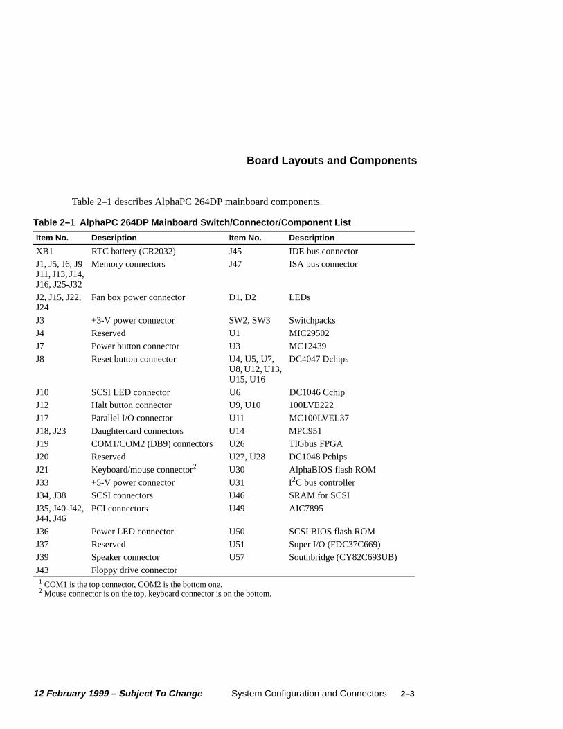
Table 2–1 describes AlphaPC 264DP mainboard components.
Table 2–1 AlphaPC 264DP Mainboard Switch/Connector/Component List
Item No. Description Item No. Description
XB1 RTC battery (CR2032) J45 IDE bus connector
J1, J5, J6, J9 J11, J13, J14, J16, J25-J32
Memory connectors J47 ISA bus connector
J2, J15, J22, J24
Fan box power connector D1, D2 LEDs
J3 +3-V power connector SW2, SW3 Switchpacks
J4 Reserved U1 MIC29502
J7 Power button connector U3 MC12439
J8 Reset button connector U4, U5, U7, U8, U12, U13, U15, U16
DC4047 Dchips
J10 SCSI LED connector U6 DC1046 Cchip
J12 Halt button connector U9, U10 100LVE222
J17 Parallel I/O connector U11 MC100LVEL37
J18, J23 Daughtercard connectors U14 MPC951
J19 COM1/COM2 (DB9) connectors1
1 COM1 is the top connector, COM2 is the bottom one.
U26 TIGbus FPGA
J20 Reserved U27, U28 DC1048 Pchips
J21 Keyboard/mouse connector2
2 Mouse connector is on the top, keyboard connector is on the bottom.
U30 AlphaBIOS flash ROM
J33 +5-V power connector U31 I2C bus controller
J34, J38 SCSI connectors U46 SRAM for SCSI
J35, J40-J42, J44, J46
PCI connectors U49 AIC7895
J36 Power LED connector U50 SCSI BIOS flash ROM
J37 Reserved U51 Super I/O (FDC37C669)
J39 Speaker connector U57 Southbridge (CY82C693UB)
J43 Floppy drive connector
12 February 1999 – Subject To Change System Configuration and Connectors 2–3

Board Layouts and Components
Figure 2–2 shows the AlphaPC 264DP daughtercard and its components, and Table 2–2 describes these components.
Figure 2–2 AlphaPC 264DP Daughtercard Switch/Connector/Component Location
U1
U2
J2U6
U5
U10
U9
U15
U17
J4
SW2
U12U13U14
U104
U103
U102
U101
J1
U11 U7
J3
U16
U18
U3U4
D4D3
D1D2
Side 1–Component Side
Side 2
D5
indicates pin 1. indicates switch 1.
U19H2
H1
2–4 System Configuration and Connectors 12 February 1999 – Subject To Change

AlphaPC 264DP Mainboard Configuration Switches
2.2 AlphaPC 264DP Mainboard Configuration Switches
The AlphaPC 264DP mainboard has two sets of programmable switches located at SW2 and SW3, as shown in Figure 2–1. These switches set the hardware configuration.
Note: There is no switchpack SW1 on production mainboards.
Figures 2–3 and 2–4 reflect the mainboard switches.
Table 2–2 AlphaPC 264DP Daughtercard Switch/Connector/Component List
Item No. Description Item No. Description
J1 Fan power U5 Microprocessor, socketed (Alpha 21264)
J2 SROM debug connector U6 Bcache tag SSRAM
J3 Daughtercard data connector U7 Reset FPGA
J4 Daughtercard power connector U11, U13, U14 lcx38
H1 21264 heat sink U12 8582 EEPROM
H2 +1.5-V regulator heat sink U15 5-V to 2.2-V converter
D1-D5 LEDs U16 tl7702b supervisor
SW2 Switchpack U17 512K×8 flash ROM, socketed
U1, U2, U9, U10, U101-104
Bcache data SSRAMs U18 74f151 multiplexer
U3 1489 U19 mic29302 3.3-V to 1.5-V regulator
U4 1488
12 February 1999 – Subject To Change System Configuration and Connectors 2–5
AlphaPC 264DP Mainboard Configuration Switches
Figure 2–3 Mainboard Switchpack 2
Figure 2–4 Mainboard Switchpack 3
21272 Speed: MHz sp2 sp1 sp0
83.3 Off On On
fsb
coa
cob
mdb
sp0
sp1
sp2
pby
Off On
AlphaBIOS Password Bypass:Off Normal operationOn Bypass AlphaBIOS password
Note: Switch defaults are in bold.SW2
FSB: Off Normal bootOn Fail-Safe Booter
Memory Timing: These switches must be kept at Off - Off.
Mini-Debugger: Off Normal SROM flowOn SROM jumps to Mini-Debugger
1
2
3
4
5
6
7
8
Note: All other combinations are reserved. This must be kept at 83.3 MHz.
cn7
cn6
cn5
cn4
cn3
cn2
spr
flash_wr
Off On
Note: Switch defaults are in bold.SW3
Flash Write Protect: Off Write enable flash ROMOn Write disable flash ROM
Reserved: This switch must be kept Off.
Reserved: Note: The switches must remain as follows:
Refer to the 21272 Specification for more information.
cn7 cn6 cn5 cn4 cn3 cn2
Off Off Off On Off Off
These switches map to the CSC register in the Cchip. They represent the following bits:
cn7cn6
cn5,4cn3cn2
For firmware usesysDC fill delay (SFD)sysDC extract delay (SED)CPU1 clock forward presetCPU0 clock forward preset
1
2
3
4
5
6
7
8
2–6 System Configuration and Connectors 12 February 1999 – Subject To Change

AlphaPC 264DP Mainboard Configuration Switches
ition rap
s is pro-
e on er to ass
witch
2.2.1 Fail-Safe Booter
The Fail-Safe Booter (FSB) utility provides an emergency recovery mechanism when the primary firmware image contained in flash memory has been corrupted. When flash memory has been corrupted, and no image can be loaded safely from the flash ROM, you can run the FSB and boot another image from a diskette that is capable of reprogramming the flash ROM.
2.2.2 Memory Timing
The memory bus timing is controlled by switches 2 and 3 of SW2 on the mainboard (see Figure 2–3). Both switches are off by default, and they must be kept off.
2.2.3 Mini-Debugger
The Alpha SROM Mini-Debugger is stored in the flash ROM and is enabled/disabled by switch 4 of SW2 on the mainboard (see Figure 2–3). The default posfor this switch is off. When this switch is on, it causes the SROM initialization to tto the Mini-Debugger after all initialization is complete, but before starting the execution of the system flash ROM code.
2.2.4 Password Bypass
AlphaBIOS provides password protection. However, if the use of passwords habeen enabled and you have forgotten the current password, password bypass vided through the use of switch 8 (pby) of SW2 on the mainboard.
Normal operation, with switch 8 in the off position (see Figure 2–3), requires a password. The password bypass function is enabled by setting the switch to thposition. This disables the AlphaBIOS password verification and enables the usset up or start up their system without the AlphaBIOS password. Password bypalso clears the password.
After this function has been enabled, to disable it and require a password, set s8 to the off position.
12 February 1999 – Subject To Change System Configuration and Connectors 2–7
AlphaPC 264DP Daughtercard Configuration Switches
.
2. efault
own 2–5
d M
2.2.5 Flash Write Protection
The AlphaPC 264DP provides write protection for the firmware flash ROM. By default, writing to the flash ROM is allowed, that is, switch 8 (flash_wr) of SW3 on the mainboard is off (see Figure 2–4).
Note: The AlphaPC 264DP will not function if switch 8 is in the on position
2.2.6 21272 Speed
The speed of the 21272 core logic chipset is determined by switches 5–7 of SWThe default positions are 5 and 6 on, 7 off. These switches must be kept in the dposition.
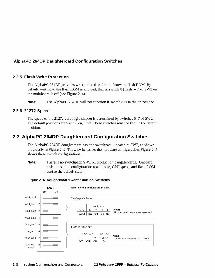
2.3 AlphaPC 264DP Daughtercard Configuration Switches
The AlphaPC 264DP daughtercard has one switchpack, located at SW2, as shpreviously in Figure 2–2. These switches set the hardware configuration. Figureshows these switch configurations.
Note: There is no switchpack SW1 on production daughtercards. Onboarresistors set the configuration (cache size, CPU speed, and flash ROuse) to the default state.
Figure 2–5 Daughtercard Configuration Switches
Note:All other combinations are reserved.
Note: Switch defaults are in bold.
vout_set0
vout_set1
vout_set2
vout_set3
flash_sel2
flash_sel1
flash_sel0
flash_sel_bypass
Off On
SW2
vout_setx
V dc 3 2 1 0
2.214 On Off On On
flash_selx flash_sel_
2 1 0 bypass
Off Off Off On
Note:All other combinations are reserved.
Set Output Voltage:
Flash ROM Select:
1
2
4
5
6
7
8
3
2–8 System Configuration and Connectors 12 February 1999 – Subject To Change

AlphaPC 264DP Mainboard Connector Pinouts
gh
2.4 AlphaPC 264DP Mainboard Connector Pinouts
This section lists the pinouts of the mainboard connectors (see Table 2–3 throuTable 2–21). See Figure 2–1 for connector locations.
2.4.1 Daughtercard Connector Pinouts
Table 2–3 shows the daughtercard connector pinouts.
Table 2–3 Daughtercard Connector Pinouts (J18, J23)
Pin Signal Pin Signal Pin Signal Pin Signal
1 vdd_3v 2 vdd_3v 3 vdd_3v 4 vdd_3v5 vdd_3v 6 vdd_3v 7 vdd_3v 8 vdd_3v9 sysdata2_l 10 sysdata0_l 11 sysdata5_l 12 sysdata3_l13 syscheck0_l 14 sysdata9_l 15 sysdata10_l 16 sysdata13_l17 sysdata14_l 18 sysdataoutclk1_l 19 sysdata16_l 20 syscheck20_l21 sysdata17_l 22 sysdata18_l 23 sysdataoutclk2_l 24 sysdata21_l25 sda 26 Gnd 27 Gnd 28 cpu_slot29 sysdata26_l 30 sysdata25_l 31 sysdatainclk3_l 32 sysdata28_l33 sysdata30_l 34 syscheck3_l 35 clkfwdreset_h 36 irq_0_h37 irq_2_h 38 irq_4_h 39 2v_pwrgood_h 40 tsu_speed041 tsu_speed1 42 clk_rdy_h 43 tsu_speed2 44 sysfillvalid_l45 sysaddin13_l 46 sysaddin8_l 47 sysaddin9_l 48 sysaddinclk_l49 sysaddout13_l 50 sysaddin7_l 51 sysaddin1_l 52 sysaddin3_l53 sysaddout14_l 54 sysaddout12_l 55 sysaddout10_l 56 sysaddoutclk_l57 sysaddout6_l 58 sysaddout0_l 59 sysaddout2_l 60 syscheck7_l61 sysaddout1_l 62 sysdata60_l 63 sysdatainclk7_l 64 sysdata52_l65 sysdata54_l 66 sysdata57_l 67 sysdataoutclk6_l 68 sysdata51_l69 sysdata49_l 70 syscheck5_l 71 sysdata46_l 72 sysdata47_l73 sysdata45_l 74 sysdata42_l 75 sysdatainclk5_l 76 sysdata41_l77 sysdataoutclk4_l 78 sysdata37_l 79 sysdata36_l 80 sysdata35_l81 sysdata32_l 82 Gnd 83 bc_config1 84 bc_config385 cpu_speed1 86 +12v_mod 87 vdd_2v_term 88 vdd_2v_term89 vdd_2v_term 90 vdd_2v_term 91 vdd_3v 92 vdd_3v93 vdd_3v 94 vdd_3v 95 vdd_3v 96 vdd_3v97 vdd_3v 98 vdd_3v 99 sysdatainclk0_l 100 sysdata6_l101 sysdata1_l 102 sysdataoutclk0_l 103 sysdata4_l 104 sysdata7_l105 sysdata8_l 106 sysdatainclk1_l 107 sysdata11_l 108 sysdata12_l
12 February 1999 – Subject To Change System Configuration and Connectors 2–9

AlphaPC 264DP Mainboard Connector Pinouts
109 sysdata15_l 110 sysdata19_l 111 sysdatainclk2_l 112 sysdata20_l113 sysdata22_l 114 sysdata23_l 115 pllbypass_h 116 srom_en_l117 sclk 118 syscheck2_l 119 sysdata24_l 120 sysdata27_l121 sysdataoutclk3_l 122 sysdata29_l 123 sysdata31_l 124 sysdataoutvalid_l125 Gnd 126 Gnd 127 fan_ok_l 128 irq_1_h129 irq_3_h 130 irq_5_h 131 mod_reset_l 132 sysaddin11_l133 sysaddin14_l 134 sysdatainvalid_l 135 sysaddin10_l 136 sysaddin12_l137 sysaddin4_l 138 sysaddin5_l 139 sysaddin2_l 140 sysaddin6_l141 sysaddout11_l 142 sysaddin0_l 143 sysaddout7_l 144 sysaddout9_l145 sysaddout8_l 146 sysaddout5_l 147 sysaddout4_l 148 sysaddout3_l149 sysdata63_l 150 sysdata62_l 151 sysdata61_l 152 sysdata59_l153 sysdataoutclk7_l 154 sysdata53_l 155 syscheck6_l 156 sysdata55_l157 sysdata56_l 158 sysdata58_l 159 sysdatainclk6_l 160 sysdata50_l161 sysdata48_l 162 sysdata44_l 163 sysdataoutclk5_l 164 sysdata43_l165 sysdata40_l 166 sysdata38_l 167 syscheck4_l 168 sysdata39_l169 sysdata34_l 170 sysdatainclk4_l 171 sysdata33_l 172 bc_config0173 bc_config2 174 cpu_speed0 175 cpu_speed2 176 −12v_mod177 vdd_2v_term 178 vdd_2v_term 179 vdd_2v_term 180 vdd_2v_term181to211
Gnd 212 pecl_clkin_h 213 pecl_clkin_l 214 Gnd
215 frameclk_h 216 frameclk_l 217to270
Gnd
Table 2–3 Daughtercard Connector Pinouts (J18, J23) (Continued)
Pin Signal Pin Signal Pin Signal Pin Signal
2–10 System Configuration and Connectors 12 February 1999 – Subject To Change

AlphaPC 264DP Mainboard Connector Pinouts
2.4.2 PCI Bus Connector Pinouts
Table 2–4 shows the PCI bus connector pinouts.
Table 2–4 PCI Bus Connector Pinouts (J35, J40–J42, J44, J46)
Pin Signal Pin Signal Pin Signal Pin Signal
A1 TRST# A2 +12V A3 TMS A4 TDIA5 Vdd A6 INTA A7 INTC A8 VddA9 — A10 Vdd A11 — A12 GndA13 Gnd A14 — A15 RST# A16 VddA17 GNT# A18 Gnd A19 — A20 AD[30]A21 +3V A22 AD[28] A23 AD[26] A24 GndA25 AD[24] A26 IDSEL A27 +3V A28 AD[22]A29 AD[20] A30 Gnd A31 AD[18] A32 AD[16]A33 +3V A34 FRAME# A35 Gnd A36 TRDY#A37 STOP# A38 STOP# A39 +3V A40 SDONEA41 SBO# A42 Gnd A43 PAR A44 AD[15]A45 +3V A46 AD[13] A47 AD[11] A48 GndA49 AD[09] A50 Not used A51 Not used A52 C/BE#[0]A53 +3V A54 AD[06] A55 AD[04] A56 GndA57 AD[02] A58 AD[00] A59 Vdd A60 REQ64#A61 Vdd A62 Vdd B1 -12V B2 TCKB3 Gnd B4 TDO B5 Vdd B6 VddB7 INTB B8 INTD B9 PRSNT1# B10 —
B11 PRSNT2# B12 Gnd B13 Gnd B14 —
B15 Gnd B16 CLK B17 Gnd B18 REQ#B19 Vdd B20 AD[31] B21 AD[29] B22 GndB23 AD[27] B24 AD[25] B25 +3V B26 C/BE#[3]B27 AD[23] B28 Gnd B29 AD[21] B30 AD[19]B31 +3V B32 AD[17] B33 C/BE#[2] B34 Gnd B35 IRDY# B36 +3V B37 DEVSEL# B38 Gnd B39 LOCK# B40 PERR# B41 +3V B42 SERR#B43 +3V B44 C/BE#[1] B45 AD[14] B46 Gnd B47 AD[12] B48 AD[10] B49 Gnd B50 Not used
B51 Not used B52 AD[08] B53 AD[07] B54 +3VB55 AD[05] B56 AD[03] B57 Gnd B58 AD[01]B59 Vdd B60 ACK64# B61 Vdd B62 Vdd
12 February 1999 – Subject To Change System Configuration and Connectors 2–11
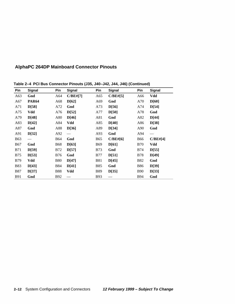
AlphaPC 264DP Mainboard Connector Pinouts
A63 Gnd A64 C/BE#[7] A65 C/BE#[5] A66 VddA67 PAR64 A68 D[62] A69 Gnd A70 D[60]A71 D[58] A72 Gnd A73 D[56] A74 D[54]A75 Vdd A76 D[52] A77 D[50] A78 Gnd A79 D[48] A80 D[46] A81 Gnd A82 D[44]A83 D[42] A84 Vdd A85 D[40] A86 D[38]A87 Gnd A88 D[36] A89 D[34] A90 Gnd A91 D[32] A92 — A93 Gnd A94 —
B63 — B64 Gnd B65 C/BE#[6] B66 C/BE#[4]B67 Gnd B68 D[63] B69 D[61] B70 VddB71 D[59] B72 D[57] B73 Gnd B74 D[55]B75 D[53] B76 Gnd B77 D[51] B78 D[49]B79 Vdd B80 D[47] B81 D[45] B82 Gnd B83 D[43] B84 D[41] B85 Gnd B86 D[39]B87 D[37] B88 Vdd B89 D[35] B90 D[33]B91 Gnd B92 — B93 — B94 Gnd
Table 2–4 PCI Bus Connector Pinouts (J35, J40–J42, J44, J46) (Continued)
Pin Signal Pin Signal Pin Signal Pin Signal
2–12 System Configuration and Connectors 12 February 1999 – Subject To Change
AlphaPC 264DP Mainboard Connector Pinouts
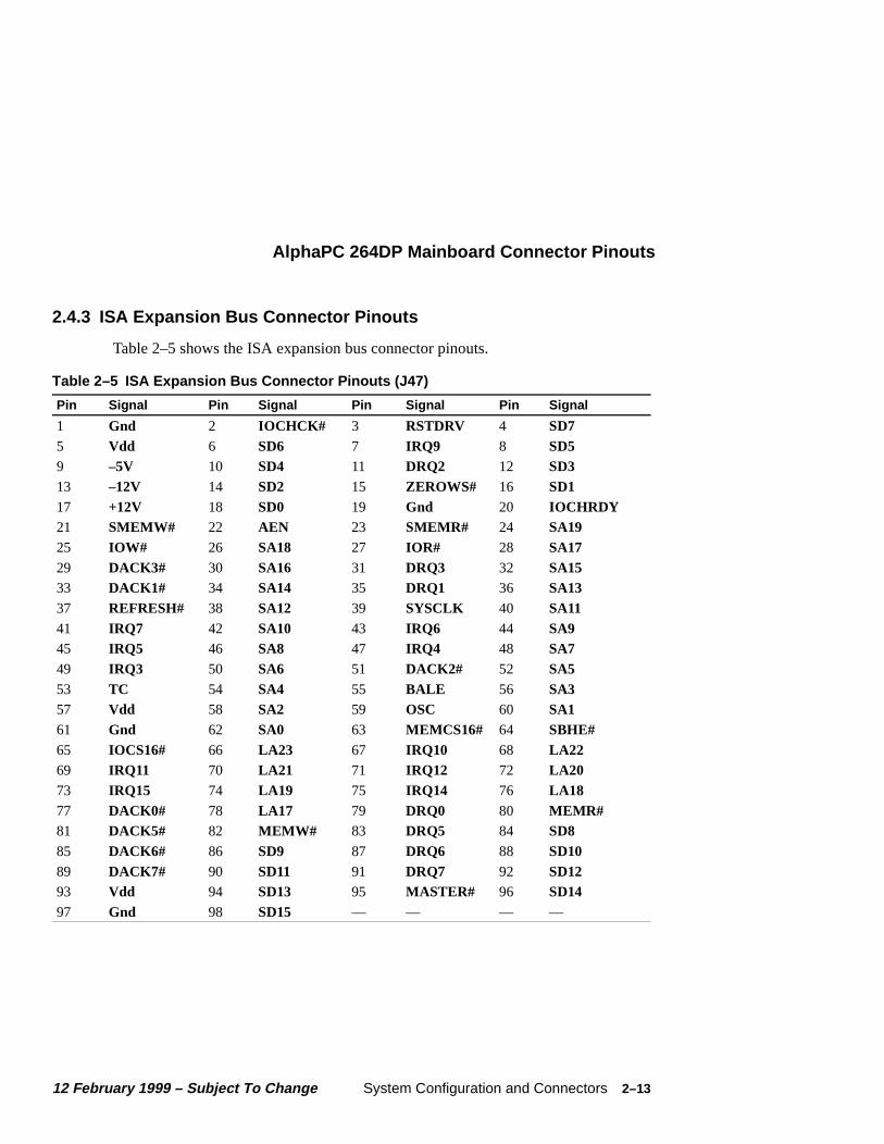
2.4.3 ISA Expansion Bus Connector Pinouts
Table 2–5 shows the ISA expansion bus connector pinouts.
Table 2–5 ISA Expansion Bus Connector Pinouts (J47)
Pin Signal Pin Signal Pin Signal Pin Signal
1 Gnd 2 IOCHCK# 3 RSTDRV 4 SD75 Vdd 6 SD6 7 IRQ9 8 SD59 –5V 10 SD4 11 DRQ2 12 SD313 –12V 14 SD2 15 ZEROWS# 16 SD117 +12V 18 SD0 19 Gnd 20 IOCHRDY21 SMEMW# 22 AEN 23 SMEMR# 24 SA1925 IOW# 26 SA18 27 IOR# 28 SA1729 DACK3# 30 SA16 31 DRQ3 32 SA1533 DACK1# 34 SA14 35 DRQ1 36 SA1337 REFRESH# 38 SA12 39 SYSCLK 40 SA1141 IRQ7 42 SA10 43 IRQ6 44 SA945 IRQ5 46 SA8 47 IRQ4 48 SA749 IRQ3 50 SA6 51 DACK2# 52 SA553 TC 54 SA4 55 BALE 56 SA357 Vdd 58 SA2 59 OSC 60 SA161 Gnd 62 SA0 63 MEMCS16# 64 SBHE#65 IOCS16# 66 LA23 67 IRQ10 68 LA2269 IRQ11 70 LA21 71 IRQ12 72 LA2073 IRQ15 74 LA19 75 IRQ14 76 LA1877 DACK0# 78 LA17 79 DRQ0 80 MEMR#81 DACK5# 82 MEMW# 83 DRQ5 84 SD885 DACK6# 86 SD9 87 DRQ6 88 SD1089 DACK7# 90 SD11 91 DRQ7 92 SD1293 Vdd 94 SD13 95 MASTER# 96 SD1497 Gnd 98 SD15 — — — —
12 February 1999 – Subject To Change System Configuration and Connectors 2–13

AlphaPC 264DP Mainboard Connector Pinouts
2.4.4 IDE Drive Bus Connector Pinouts
Table 2–6 shows the IDE drive bus connector pinouts.
2.4.5 Ultra SCSI Bus Connector Pinouts
Table 2–7 shows the Ultra SCSI bus connector pinouts.
Table 2–6 IDE Drive Bus Connector Pinouts (J45)
Pin Signal Pin Signal Pin Signal Pin Signal
1 DRST 2 Gnd 3 IDE_D7 4 IDE_D85 IDE_D6 6 IDE_D9 7 IDE_D5 8 IDE_D109 IDE_D4 10 IDE_D11 11 IDE_D3 12 IDE_D1213 IDE_D2 14 IDE_D13 15 IDE_D1 16 IDE_D1417 IDE_D0 18 IDE_D15 19 Gnd 20 NC (key pin)
21 IDE_REQ0 22 Gnd 23 IDE_IOW1# 24 Gnd 25 IOR# 26 Gnd 27 CHRDY 28 BALE29 MACK 30 Gnd 31 IRQ 32 IOCS16#33 ADDR1 34 NC 35 ADDR0 36 ADDR237 CS0# 38 CS1# 39 ACT# 40 Gnd
Table 2–7 Ultra SCSI Bus Connector Pinouts (J34, J38)
Pin Signal Pin Signal Pin Signal Pin Signal
1 Gnd 2 Gnd 3 Gnd 4 Gnd5 Gnd 6 Gnd 7 Gnd 8 Gnd9 Gnd 10 Gnd 11 Gnd 12 Gnd13 Gnd 14 Gnd 15 Gnd 16 Gnd17 termpwr 18 termpwr 19 NC 20 Gnd21 Gnd 22 Gnd 23 Gnd 24 Gnd25 Gnd 26 Gnd 27 Gnd 28 Gnd29 Gnd 30 Gnd 31 Gnd 32 Gnd33 Gnd 34 Gnd 35 scd12 36 scd1337 scd14 38 scd15 39 scdph 40 scd041 scd1 42 scd2 43 scd3 44 scd445 scd5 46 scd6 47 scd7 48 scdpl49 Gnd 50 Gnd 51 termpwr 52 termpwr53 NC 54 Gnd 55 atn 56 Gnd
2–14 System Configuration and Connectors 12 February 1999 – Subject To Change

AlphaPC 264DP Mainboard Connector Pinouts
2.4.6 SDRAM DIMM Connector Pinouts
Table 2–8 shows the SDRAM DIMM connector pinouts.
57 bsy 58 ack 59 reset 60 msg61 sel 62 cd 63 req 64 io65 scd8 66 scd9 67 scd10 68 scd11
Table 2–8 SDRAM DIMM Connector Pinouts (J1, J5, J6, J9, J11, J13, J14, J16, J25–J32)
Pin Signal Pin Signal Pin Signal Pin Signal
1 Vdd 2 NC 3 NC 4 NC
5 NC 6 NC 7 NC 8 Vss9 dq67 10 dq66 11 Vdd 12 dq6513 dq64 14 Vss 15 dq63 16 dq6217 NC 18 dq61 19 dq60 20 Vdd21 NC 22 NC 23 Vss 24 NC
25 NC 26 Vdd 27 dq51 28 dq5029 Vss 30 dq49 31 dq48 32 Vdd33 dq43 34 dq42 35 Vss 36 dq4137 dq40 38 Vdd 39 a4 40 a541 Vss 42 a8 43 a9 44 Vdd45 NC 46 cke0 47 Vss 48 cas#49 NC 50 Vdd 51 Vss 52 ras#53 Vss 54 cs2# 55 a11 56 Vdd57 a0 58 a1 59 Vss 60 dq3561 dq34 62 Vdd 63 dq33 64 dq3265 Vss 66 dq27 67 dq26 68 Vdd69 dq25 70 dq24 71 Vss 72 dq1973 dq18 74 Vdd 75 dq17 76 dq1677 Vss 78 NC 79 NC 80 Vdd81 dq15 82 dq14 83 Vss 84 dq1385 dq12 86 Vdd 87 dq7 88 dq689 Vss 90 dq5 91 dq4 92 Vdd93 NC 94 NC 95 NC 96 NC
97 NC 98 scl 99 NC 100 Vss
Table 2–7 Ultra SCSI Bus Connector Pinouts (J34, J38) (Continued)
Pin Signal Pin Signal Pin Signal Pin Signal
12 February 1999 – Subject To Change System Configuration and Connectors 2–15

AlphaPC 264DP Mainboard Connector Pinouts
101 NC 102 NC 103 Vss 104 rege105 rfu 106 rfu 107 NC 108 dq71109 dq70 110 Vss 111 dq69 112 dq68113 Vdd 114 NC 115 Vss 116 NC
117 dq59 118 dq58 119 Vss 120 dq57121 dq56 122 Vdd 123 dq55 124 dq54125 Vss 126 dq53 127 dq52 128 Vdd129 dq47 130 dq46 131 Vss 132 dq45133 dq44 134 Vdd 135 dq39 136 dq38137 Vss 138 dq37 139 dq36 140 Vdd141 a6 142 a7 143 Vss 144 bs0145 NC 146 Vdd 147 dqm 148 we#149 Vss 150 NC 151 clk0 152 Vdd153 NC 154 cs0# 155 Vss 156 ba1157 a10/ap 158 Vdd 159 a2 160 a3161 Vss 162 dq31 163 dq30 164 Vdd165 dq29 166 dq28 167 Vss 168 dq23169 dq22 170 Vdd 171 dq21 172 dq20173 Vss 174 NC 175 NC 176 Vdd177 NC 178 Vss 179 Vss 180 NC
181 NC 182 Vdd 183 dq11 184 dq10185 Vss 186 dq9 187 dq8 188 Vdd189 dq3 190 dq2 191 Vss 192 dq1193 dq0 194 sda 195 sa0 196 sa1197 sa2 198 Vdd 199 NC 200 NC
Table 2–8 SDRAM DIMM Connector Pinouts (J1, J5, J6, J9, J11, J13, J14, J16, J25–J32) (Continued)
Pin Signal Pin Signal Pin Signal Pin Signal
2–16 System Configuration and Connectors 12 February 1999 – Subject To Change

AlphaPC 264DP Mainboard Connector Pinouts
2.4.7 Diskette (Floppy) Drive Bus Connector Pinouts
Table 2–9 shows the diskette (floppy) drive bus connector pinouts.
2.4.8 Parallel Bus Connector Pinouts
Table 2–10 shows the parallel bus connector pinouts.
Table 2–9 Diskette (Floppy) Drive Bus Connector Pinouts (J43)
Pin Signal Pin Signal Pin Signal Pin Signal
1 Gnd 2 DRVDEN0 3 Gnd 4 NC
5 Gnd 6 DRVDEN1 7 Gnd 8 INDEX9 Gnd 10 MTR0 11 Gnd 12 DS113 Gnd 14 DS0 15 Gnd 16 MTR117 Gnd 18 DIR 19 Gnd 20 STEP21 Gnd 22 WDATA 23 Gnd 24 WGATE25 Gnd 26 TRK0 27 Gnd 28 WRTPRT29 Gnd 30 RDATA 31 Gnd 32 HDSEL33 Gnd 34 DSKCHG — — — —
Table 2–10 Parallel Bus Connector Pinouts (J17)
Pin Signal Pin Signal Pin Signal Pin Signal
1 PSTB 2 PD0 3 PD1 4 PD25 PD3 6 PD4 7 PD5 8 PD69 PD7 10 PACK 11 PBUSY 12 PE13 PSLCT 14 PAFD 15 PAR_ERROR 16 PINIT17 PSLIN 18 Gnd 19 Gnd 20 Gnd 21 Gnd 22 Gnd 23 Gnd 24 Gnd 25 Gnd — — — — — —
12 February 1999 – Subject To Change System Configuration and Connectors 2–17

AlphaPC 264DP Mainboard Connector Pinouts
2.4.9 COM1/COM2 Serial Line Connector Pinouts
Table 2–11 shows the COM1/COM2 serial line connector pinouts.
2.4.10 Keyboard/Mouse Connector Pinouts
Table 2–12 shows the keyboard/mouse connector pinouts.
Table 2–11 COM1/COM2 Serial Line Connector Pinouts (J19)
COM1 Pin (Top) COM1 Signal
COM2 Pin (Bottom) COM2 Signal
1 DCD1 10 DCD22 SIN1 11 SIN23 SOUT1 12 SOUT24 DTR1 13 DTR25 Gnd 14 Gnd6 DSR1 15 DSR27 RTS1 16 RTS28 CTS1 17 CTS29 RI1 18 RI2
Table 2–12 Keyboard/Mouse Connector Pinouts (J21)
Keyboard Pin (Top) Keyboard Signal
Mouse Pin (Bottom) Mouse Signal
1 KBDATA 7 MSDATA2 NC 8 NC
3 Gnd 9 Gnd 4 Vdd 10 Vdd5 KBCLK 11 MSCLK6 NC 12 NC
2–18 System Configuration and Connectors 12 February 1999 – Subject To Change
AlphaPC 264DP Mainboard Connector Pinouts
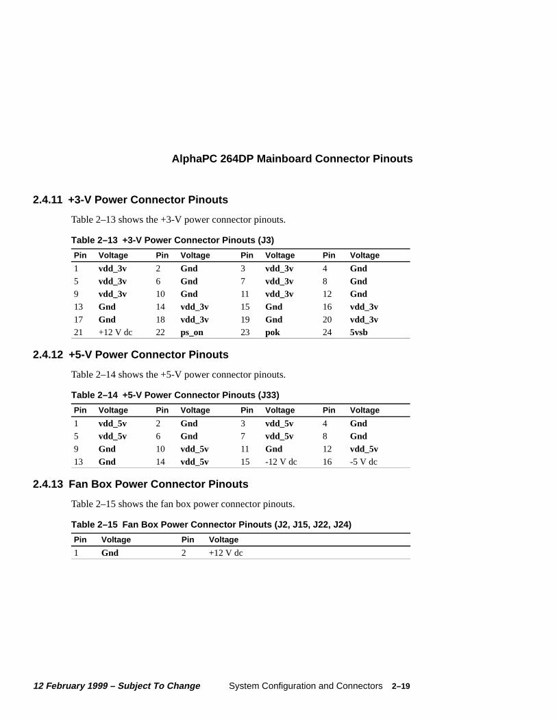
2.4.11 +3-V Power Connector Pinouts
Table 2–13 shows the +3-V power connector pinouts.
2.4.12 +5-V Power Connector Pinouts
Table 2–14 shows the +5-V power connector pinouts.
2.4.13 Fan Box Power Connector Pinouts
Table 2–15 shows the fan box power connector pinouts.
Table 2–13 +3-V Power Connector Pinouts (J3)
Pin Voltage Pin Voltage Pin Voltage Pin Voltage
1 vdd_3v 2 Gnd 3 vdd_3v 4 Gnd5 vdd_3v 6 Gnd 7 vdd_3v 8 Gnd9 vdd_3v 10 Gnd 11 vdd_3v 12 Gnd13 Gnd 14 vdd_3v 15 Gnd 16 vdd_3v17 Gnd 18 vdd_3v 19 Gnd 20 vdd_3v21 +12 V dc 22 ps_on 23 pok 24 5vsb
Table 2–14 +5-V Power Connector Pinouts (J33)
Pin Voltage Pin Voltage Pin Voltage Pin Voltage
1 vdd_5v 2 Gnd 3 vdd_5v 4 Gnd5 vdd_5v 6 Gnd 7 vdd_5v 8 Gnd9 Gnd 10 vdd_5v 11 Gnd 12 vdd_5v13 Gnd 14 vdd_5v 15 -12 V dc 16 -5 V dc
Table 2–15 Fan Box Power Connector Pinouts (J2, J15, J22, J24)
Pin Voltage Pin Voltage
1 Gnd 2 +12 V dc
12 February 1999 – Subject To Change System Configuration and Connectors 2–19

AlphaPC 264DP Mainboard Connector Pinouts
2.4.14 Speaker Connector Pinouts
Table 2–16 shows the speaker connector pinouts.
2.4.15 Halt Button Connector Pinouts
Table 2–17 shows the halt button connector pinouts.
2.4.16 Reset Button Connector Pinouts
Table 2–18 shows the reset button connector pinouts.
2.4.17 System Power Button Connector Pinouts
Table 2–19 shows the system power button connector pinouts.
Table 2–16 Speaker Connector Pinouts (J39)
Pin Signal Description
1 spkr Speaker input
2 vdd_5v —
3 Gnd —
4 vdd_5v —
Table 2–17 Halt Button Connector Pinouts (J12)
Pin Signal Description
1 halt_button Halt system (for Tru64 UNIX only)
2 vdd_5v —
Table 2–18 Reset Button Connector Pinouts (J8)
Pin Signal Description
1 reset_button Reset system
2 vdd_5v —
Table 2–19 System Power Button Connector Pinouts (J7)
Pin Signal Description
1 ps_on System power on/off
2 Gnd —
2–20 System Configuration and Connectors 12 February 1999 – Subject To Change
AlphaPC 264DP Mainboard Connector Pinouts
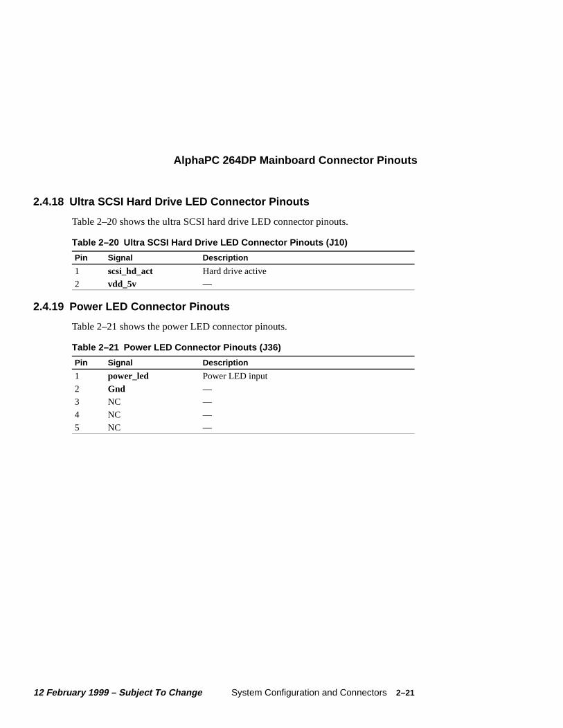
2.4.18 Ultra SCSI Hard Drive LED Connector Pinouts
Table 2–20 shows the ultra SCSI hard drive LED connector pinouts.
2.4.19 Power LED Connector Pinouts
Table 2–21 shows the power LED connector pinouts.
Table 2–20 Ultra SCSI Hard Drive LED Connector Pinouts (J10)
Pin Signal Description
1 scsi_hd_act Hard drive active
2 vdd_5v —
Table 2–21 Power LED Connector Pinouts (J36)
Pin Signal Description
1 power_led Power LED input
2 Gnd —
3 NC —
4 NC —
5 NC —
12 February 1999 – Subject To Change System Configuration and Connectors 2–21

AlphaPC 264DP Daughtercard Connector Pinouts
2.5 AlphaPC 264DP Daughtercard Connector Pinouts
This section lists the pinouts of the AlphaPC 264DP daughtercard connectors (see Table 2–22 through Table 2–25). See Figure 2–2 for connector locations.
2.5.1 Microprocessor Fan Power Connector Pinouts
Table 2–22 shows the microprocessor fan power connector pinouts.
2.5.2 SROM Test Data Input Connector Pinouts
Table 2–23 shows the SROM test data input connector pinouts.
2.5.3 AlphaPC 264DP Daughtercard Connector Pinouts
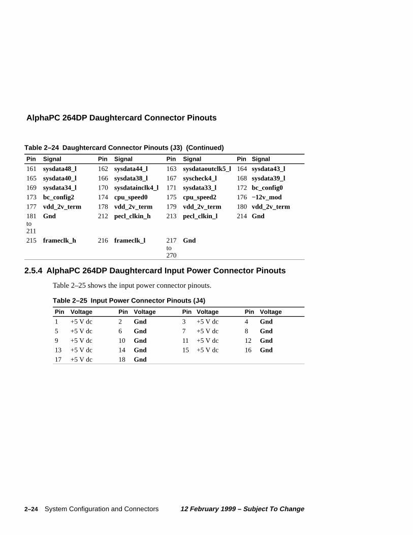
Table 2–24 shows the AlphaPC 264DP daughtercard connector pinouts.
Table 2–22 Microprocessor Fan Power Connector Pinouts (J1)
Pin Signal Description
1, 6 +12 V dc —
2, 5 Gnd —
3, 4 fan_conn_l Fan connected
Table 2–23 SROM Test Data Input Connector Pinouts (J2)
Pin Signal Description
1 NC —
2 srom_clk_l Clock out
3 Gnd —
4 NC —
5 test_srom_d_l SROM serial data in
6 NC —
Table 2–24 Daughtercard Connector Pinouts (J3)
Pin Signal Pin Signal Pin Signal Pin Signal
1 vdd_3v 2 vdd_3v 3 vdd_3v 4 vdd_3v5 vdd_3v 6 vdd_3v 7 vdd_3v 8 vdd_3v9 sysdata2_l 10 sysdata0_l 11 sysdata5_l 12 sysdata3_l13 syscheck0_l 14 sysdata9_l 15 sysdata10_l 16 sysdata13_l17 sysdata14_l 18 sysdataoutclk1_l 19 sysdata16_l 20 syscheck20_l21 sysdata17_l 22 sysdata18_l 23 sysdataoutclk2_l 24 sysdata21_l
2–22 System Configuration and Connectors 12 February 1999 – Subject To Change
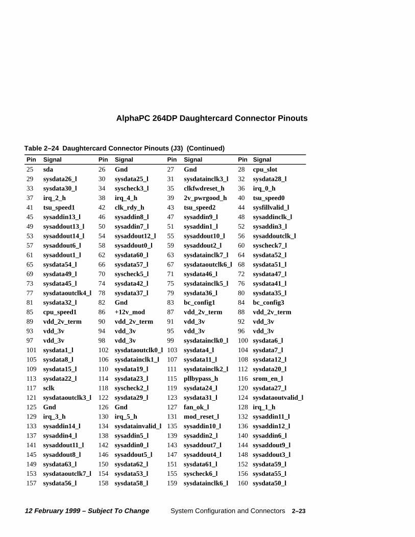
AlphaPC 264DP Daughtercard Connector Pinouts
25 sda 26 Gnd 27 Gnd 28 cpu_slot29 sysdata26_l 30 sysdata25_l 31 sysdatainclk3_l 32 sysdata28_l33 sysdata30_l 34 syscheck3_l 35 clkfwdreset_h 36 irq_0_h37 irq_2_h 38 irq_4_h 39 2v_pwrgood_h 40 tsu_speed041 tsu_speed1 42 clk_rdy_h 43 tsu_speed2 44 sysfillvalid_l45 sysaddin13_l 46 sysaddin8_l 47 sysaddin9_l 48 sysaddinclk_l49 sysaddout13_l 50 sysaddin7_l 51 sysaddin1_l 52 sysaddin3_l53 sysaddout14_l 54 sysaddout12_l 55 sysaddout10_l 56 sysaddoutclk_l57 sysaddout6_l 58 sysaddout0_l 59 sysaddout2_l 60 syscheck7_l61 sysaddout1_l 62 sysdata60_l 63 sysdatainclk7_l 64 sysdata52_l65 sysdata54_l 66 sysdata57_l 67 sysdataoutclk6_l 68 sysdata51_l69 sysdata49_l 70 syscheck5_l 71 sysdata46_l 72 sysdata47_l73 sysdata45_l 74 sysdata42_l 75 sysdatainclk5_l 76 sysdata41_l77 sysdataoutclk4_l 78 sysdata37_l 79 sysdata36_l 80 sysdata35_l81 sysdata32_l 82 Gnd 83 bc_config1 84 bc_config385 cpu_speed1 86 +12v_mod 87 vdd_2v_term 88 vdd_2v_term89 vdd_2v_term 90 vdd_2v_term 91 vdd_3v 92 vdd_3v93 vdd_3v 94 vdd_3v 95 vdd_3v 96 vdd_3v97 vdd_3v 98 vdd_3v 99 sysdatainclk0_l 100 sysdata6_l101 sysdata1_l 102 sysdataoutclk0_l 103 sysdata4_l 104 sysdata7_l105 sysdata8_l 106 sysdatainclk1_l 107 sysdata11_l 108 sysdata12_l109 sysdata15_l 110 sysdata19_l 111 sysdatainclk2_l 112 sysdata20_l113 sysdata22_l 114 sysdata23_l 115 pllbypass_h 116 srom_en_l117 sclk 118 syscheck2_l 119 sysdata24_l 120 sysdata27_l121 sysdataoutclk3_l 122 sysdata29_l 123 sysdata31_l 124 sysdataoutvalid_l125 Gnd 126 Gnd 127 fan_ok_l 128 irq_1_h129 irq_3_h 130 irq_5_h 131 mod_reset_l 132 sysaddin11_l133 sysaddin14_l 134 sysdatainvalid_l 135 sysaddin10_l 136 sysaddin12_l137 sysaddin4_l 138 sysaddin5_l 139 sysaddin2_l 140 sysaddin6_l141 sysaddout11_l 142 sysaddin0_l 143 sysaddout7_l 144 sysaddout9_l145 sysaddout8_l 146 sysaddout5_l 147 sysaddout4_l 148 sysaddout3_l149 sysdata63_l 150 sysdata62_l 151 sysdata61_l 152 sysdata59_l153 sysdataoutclk7_l 154 sysdata53_l 155 syscheck6_l 156 sysdata55_l157 sysdata56_l 158 sysdata58_l 159 sysdatainclk6_l 160 sysdata50_l
Table 2–24 Daughtercard Connector Pinouts (J3) (Continued)
Pin Signal Pin Signal Pin Signal Pin Signal
12 February 1999 – Subject To Change System Configuration and Connectors 2–23
AlphaPC 264DP Daughtercard Connector Pinouts
2.5.4 AlphaPC 264DP Daughtercard Input Power Connector Pinouts
Table 2–25 shows the input power connector pinouts.
161 sysdata48_l 162 sysdata44_l 163 sysdataoutclk5_l 164 sysdata43_l165 sysdata40_l 166 sysdata38_l 167 syscheck4_l 168 sysdata39_l169 sysdata34_l 170 sysdatainclk4_l 171 sysdata33_l 172 bc_config0173 bc_config2 174 cpu_speed0 175 cpu_speed2 176 −12v_mod177 vdd_2v_term 178 vdd_2v_term 179 vdd_2v_term 180 vdd_2v_term181to211
Gnd 212 pecl_clkin_h 213 pecl_clkin_l 214 Gnd
215 frameclk_h 216 frameclk_l 217to270
Gnd
Table 2–25 Input Power Connector Pinouts (J4)
Pin Voltage Pin Voltage Pin Voltage Pin Voltage
1 +5 V dc 2 Gnd 3 +5 V dc 4 Gnd5 +5 V dc 6 Gnd 7 +5 V dc 8 Gnd9 +5 V dc 10 Gnd 11 +5 V dc 12 Gnd13 +5 V dc 14 Gnd 15 +5 V dc 16 Gnd17 +5 V dc 18 Gnd
Table 2–24 Daughtercard Connector Pinouts (J3) (Continued)
Pin Signal Pin Signal Pin Signal Pin Signal
2–24 System Configuration and Connectors 12 February 1999 – Subject To Change

Power Requirements
3Power and Environmental Requirements
This chapter describes the AlphaPC 264DP power and environmental requirements and physical board parameters, for both the mainboard and the daughtercard.
3.1 Power Requirements
The mainboard has a maximum total power dissipation of 215 W, excluding any disk drives. Each daughtercard has a maximum total power dissipation of 129 W. Table 3–1 lists the current requirement for each dc supply voltage.
Table 3–1 Power Supply DC Current Requirements
Voltage/Tolerance Current
Mainboard
+3.3 V dc, ±5% 30.0 A
+5 V dc, ±5% 20.0 A
5 VSB dc, ±5% 1.0 A
+12 V dc, ±5% 0.8 A
–12 V dc, ±5% 0.1 A
Daughtercard
+3.3 V dc, ±5% 5.0 A
+5 V dc, ±5% 22.0 A
+12 V dc, ±5% 0.1 A
–12 V dc, ±5% 0.05 A
12 February 1999 – Subject To Change Power and Environmental Requirements 3–1

Environmental Requirements
p’s nts of
e
Caution: Fan sensor required. The 21264 microprocessor cooling fan must have a built-in sensor that will drive a signal if the airflow stops. The sensor is connected to power connector J1. When the signal is generated, it resets the system.
3.2 Environmental Requirements
The 21264 microprocessor is cooled by a small fan blowing directly into the chiheat sink. The daughtercard is designed to run efficiently by using only this fan.Additional fans may be necessary depending upon cabinetry and the requiremeplug-in cards.
The AlphaPC 264DP mainboard and daughtercard are specified to run within thenvironment listed in Table 3–2.
3.3 Physical Parameters
The mainboard is a printed-wiring board (PWB) with the following dimensions:
• Length: 42.11 cm (16.58 in ±0.0005 in)
• Width: 33.02 cm (13.0 in ±0.0005 in)
• Height: 3.81 cm (1.5 in)
The daughtercard is a PWB with the following dimensions:
• Length: 30.48 cm (12.0 in ±0.0005 in)
• Width: 14.99 cm (5.905 in ±0.0005 in)
• Height: 6.40 cm (2.52 in ±0.0005 in)
Table 3–2 AlphaPC 264DP Environmental Requirements
Parameter Specification
Operating temperature 10°C to 40°C (50°F to 104°F)
Storage temperature –55°C to 125°C (–67°F to 257°F)
Relative humidity 10% to 90% with maximum wet bulb temperature28°C (82°F) and minimum dew point 2°C (36°F)
Rate of (dry bulb) temperature change 11°C/hour ±2°C/hour (20°F/hour ±4°F/hour)
3–2 Power and Environmental Requirements 12 February 1999 – Subject To Change

AlphaPC 264DP Hole and Connector Specifications
3.4 AlphaPC 264DP Hole and Connector Specifications
Figure 3–1 shows the AlphaPC 264DP mainboard’s hole specifications.
Figure 3–1 AlphaPC 264DP Mainboard Hole Specifications
228.09 mm (8.980 in.)
78.26 mm (3.081 in.)
76.33 mm (3.005 in.)
15.27 mm (.601 in.)
4X 322.58 mm (12.700 in.)
180.98 mm (7.125 in.)
160.02 mm (6.300 in.)
140.21 mm (5.520 in.)
12.83 mm (.505 in.)
2X 6.35 mm (.250 in.)
0.0
0
0.002X 5.08 mm (.200 in.)
16.26 mm (.640 in.)
18X 3.99 mm (.157 in.)Æ
2X 123.95 mm (4.880 in.)
128.78 mm (5.070 in.)
229.36 mm (9.030 in.)
2X 283.72 mm (11.170 in.)
Æ 8.89 mm (.350 in.)
AREA TO BE FREE OF
COMP & ETCH EXCEPT
FOR CHASSIS 7 SYSTEM GROUND
317.50 mm (12.500 in.)
397.63 mm (15.655 in.)
7.87 mm (.310 in.)
124.97 mm (4.920 in.)
215.90 mm (8.500 in.) 324.99 mm (12.795 in.)
2X 416.05 mm (16.380 in.)
413.51 mm (16.280 in.)
255.27 mm (10.050 in.)
LK98-0001A
387.29 mm (15.248 in.)
393.39 mm (15.488 in.)
2X 12.28 mm (.484 in.)
3X 5.08 mm (.200 in.)
407.79 mm (16.055 in.)
325.12 mm (12.800 in.)
12 February 1999 – Subject To Change Power and Environmental Requirements 3–3

AlphaPC 264DP Hole and Connector Specifications
Figure 3–2 shows the mainboard’s connector specifications.
Figure 3–2 AlphaPC 264DP Mainboard Connector Specifications
40.95 mm (1.612 in.)
103.53 mm (4.076 in.)
2X 120.64 mm (4.750 in.)
148.59 mm (5.850 in.)
ISA
330.20 mm (13.000 in.)
9.66 mm (.380 in.)
30.29 mm (1.193 in.)
50.61 mm (1.993 in.)
70.93 mm (2.793 in.)
91.25 mm (3.593 in.)
111.57 mm (4.393 in.)
131.89 mm (5.193 in.)
191.01 mm (7.520 in.)
2X Ø 3.50 mm (.138 in.)
217.48 mm (8.562 in.)223.58 mm (8.802 in.)
358.39 mm (14.110 in.)
360.68 mm (14.200 in.)
2X 323.60 mm (12.740 in.)
LK98-0002A319.53 mm (12.580 in.)
318.29 mm (12.531 in.)
312.55 mm (12.305 in.)
294.64 mm (11.600 in.)
16X 172.08 mm (6.775 in.)
140.97 mm (5.550 in.)
2X 85.93 mm (3.383 in.)
2X 10.92 mm (.430 in.)
421.13 mm (16.580 in.)
412.87 mm (16.255 in.)411.93 mm (16.218 in.)
403.04 mm (15.868 in.)394.15 mm (15.518 in.)
385.26 mm (15.168 in.)376.37 mm (14.818 in.)367.48 mm (14.468 in.)358.59 mm (14.118 in.)349.70 mm (13.768 in.)333.50 mm (13.130 in.)
216.mm (8.542 in.)
203.65 mm (8.018 in.)194.76 mm (7.669 in.)185.87 mm (7.318 in.)176.98 mm (6.968 in.)168.09 mm (6.618 in.)159.20 mm (6.268 in.)150.31 mm (5.918 in.)141.42 mm (5.568 in.)
125.09 mm (4.925 in.)113.66 mm (4.475 in.)
12.22 mm (.481 in.)
4.69 mm(.185 in.)
NO COMP,NO ETCHFAR SIDE3X
3X7.62 mm(.300 in.)
3X7.62 mm(.300 in.)
NO COMP, NO ETCH2X
2X 12.82 mm (.505 in.)
6X 290.25 mm (11.427 in.)
306.07 mm (12.050 in.)
321.93 mm (12.675 in.)
2.49 mm REF(.098 in.)
0.00
0.00
3–4 Power and Environmental Requirements 12 February 1999 – Subject To Change

AlphaPC 264DP Hole and Connector Specifications
Figure 3–3 shows the top and side views of the mainboard’s I/O connectors.
Figure 3–3 AlphaPC 264DP Mainboard I/O Connector Specifications
12 February 1999 – Subject To Change Power and Environmental Requirements 3–5

AlphaPC 264DP Daughtercard Hole Specification
3.5 AlphaPC 264DP Daughtercard Hole Specification
Figure 3–4 shows the hole specifications for the daughtercard.
Figure 3–4 AlphaPC 264DP Daughtercard Hole Specification—Component Side
2× 5.08 mm(.2 in.)
5.08 mm(.2 in.)
2× 5.08 mm(.2 in.)
5.08 mm(.2 in.)
135.5 mm(5.335 in.)
304.80 mm(12.000 in.)
149.99 mm(5.905 in.)
223.93 mm(8.816 in.)
3× φ 3.99 mm(.157 in.)
3–6 Power and Environmental Requirements 12 February 1999 – Subject To Change

21272 Core Logic Chipset Introduction
e,
ro-it
4Functional Description
This chapter describes the functional operation of the AlphaPC 264DP. It introduces the 21272 core logic chipset (21272) and describes its implementation with the 21264 microprocessors and their supporting memory and I/O devices.
Information, such as bus timing and protocol, found in other specifications, data sheets, and reference documentation is not duplicated here.
Note : For detailed descriptions of chipset logic, operations, and transactions, refer to the 21272 chips’ specification. For details of the PCI interfacrefer to the PCI System Design Guide and the PCI Local Bus Specifica-tion.
4.1 21272 Core Logic Chipset Introduction
The 21272 provides a solution for designers developing uniprocessor or dual-pcessor systems using the 21264 microprocessor. The chipset provides a 256-bmemory interface and includes the following three gate arrays:
• Cchip: Address and commands, 432-pin ESBGA
• Dchip: Data path, 304-pin ESBGA
• Pchip: PCI interface, 304-pin ESBGA
12 February 1999 – Subject To Change Functional Description 4–1
Cchip Functional Overview
4.2 Cchip Functional Overview
The Cchip provides the control interface between the 21264 and 21272 chipset. In addition, it provides control for the Dchips and Pchips. It also controls the memory subsystem and TIGbus. The Cchip performs the following functions:
• Maintains queues to store addresses and commands• Controls and moves data to and from arrays of main memory• Responds to commands from the CPU• Supports interrupts and flash ROM via the TIGbus
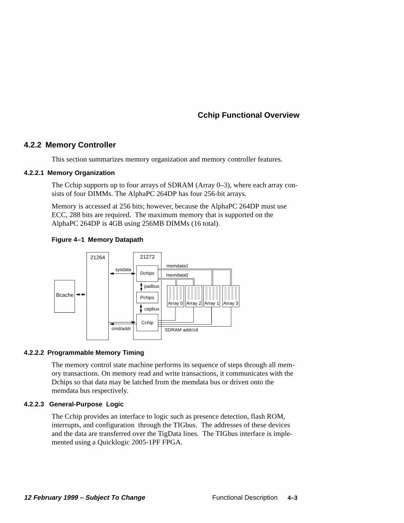
On the AlphaPC 264DP, the Cchip controls four arrays of SDRAM DIMMs. The DIMMs can range in size from 32MB to 256MB. Note that there are two separate 256-bit paths and four arrays (two on each bus) on the AlphaPC 264DP.
The components of the memory subsystem are distributed between the Cchip and the Dchips. Together, the chips serve as an interface between the CPU and memory subsystem (see Figure 4–1).
The following list summarizes the major features of the Cchip:
• Accepts requests from the Pchip and CPU
• Orders the arriving requests
• Selects the request and issues controls to the DRAMs
• Issues probes to the CPU for the selected requests
• Translates CPU PIO address to PCI and CSR addresses
• Issues commands to the Pchip for the selected request
• Issues responses to the Dchip for the DRAM accesses, the probe, and Pchip responses
• Controls the TIGbus to manage interrupts and maintains CSRs, including those that represent interrupt status
4.2.1 CPU Interface
The CPU and Cchip communicate with each other through the system port. The sys-tem port is made up of unidirectional address and command buses. The Cchip system interface logic decodes the sysPort address for both CPU and DMA requests to determine the action to take. It supports cacheable memory accesses, programmed I/O, interrupts, Tig addresses, as well as accesses to 21272 CSR space.
4–2 Functional Description 12 February 1999 – Subject To Change
Cchip Functional Overview
con-
se
4.2.2 Memory Controller
This section summarizes memory organization and memory controller features.
4.2.2.1 Memory Organization
The Cchip supports up to four arrays of SDRAM (Array 0–3), where each arraysists of four DIMMs. The AlphaPC 264DP has four 256-bit arrays.
Memory is accessed at 256 bits; however, because the AlphaPC 264DP must uECC, 288 bits are required. The maximum memory that is supported on the AlphaPC 264DP is 4GB using 256MB DIMMs (16 total).
Figure 4–1 Memory Datapath
4.2.2.2 Programmable Memory Timing
The memory control state machine performs its sequence of steps through all mem-ory transactions. On memory read and write transactions, it communicates with the Dchips so that data may be latched from the memdata bus or driven onto the memdata bus respectively.
4.2.2.3 General-Purpose Logic
The Cchip provides an interface to logic such as presence detection, flash ROM, interrupts, and configuration through the TIGbus. The addresses of these devices and the data are transferred over the TigData lines. The TIGbus interface is imple-mented using a Quicklogic 2005-1PF FPGA.
memdata1
memdata0
2127221264
Dchips
PchipsArray 3Array 1Array 2Array 0
Cchip
SDRAM addr/ctl
Bcache
padbus
capbus
sysdata
cmd/addr
12 February 1999 – Subject To Change Functional Description 4–3
Dchip Functional Overview
4.3 Dchip Functional Overview
This section provides a functional overview of the Dchips and describes the follow-ing data bus configurations:
• sysdata bus, between the Dchips and the CPUs
• memdata bus, between the Dchips and the memory arrays
• padbus, between the Dchips and the Pchips
The Dchips provide the data path from the 21264 to main memory. Although a mini-mum of two chips are required for the memory interface using the 21272, eight chips are used for the interface on the AlphaPC 264DP.
The chips contain the CPU, Pchip, and memory interface data paths, which includes DMA and PIO queues.
The Dchips interface to the CPU using the sysdata bus. It interfaces with each Pchip through the 32-bit padbus (communications path between the Pchip and Dchips, padbus0 to Pchip0 and padbus1 to Pchip1). The Dchips function as the data path for the CPU, memory, and I/O subsystem, and contain the following data path functions:
• DMA write data/PIO read data queue
• DMA read data/PIO write data queue
• Queues to allow full bandwidth transfers from memory to the CPU
• Queue to hold old memory data to be merged with the Pchip data for DMA writes
4.3.1 Sysdata Bus
The sysdata bus, between the Dchips and each CPU, passes 128 bits of data (64 bits [8 bytes] from each CPU). It is connected as follows:
• Dchip 0 connects to each of the two byte 0s.
• Dchip 1 connects to each of the two byte 1s.
• Dchip 7 connects to each of the two byte 7s.
Note: The bytes correspond to the bytes from CPU0 and CPU1.
4–4 Functional Description 12 February 1999 – Subject To Change
Dchip Functional Overview
he
4.3.2 Memdata Bus
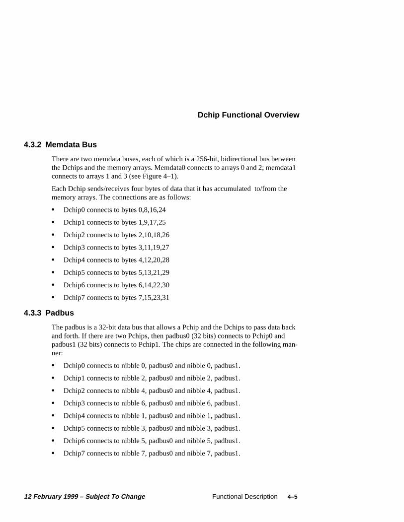
There are two memdata buses, each of which is a 256-bit, bidirectional bus between the Dchips and the memory arrays. Memdata0 connects to arrays 0 and 2; memdata1 connects to arrays 1 and 3 (see Figure 4–1).
Each Dchip sends/receives four bytes of data that it has accumulated to/from tmemory arrays. The connections are as follows:
• Dchip0 connects to bytes 0,8,16,24
• Dchip1 connects to bytes 1,9,17,25
• Dchip2 connects to bytes 2,10,18,26
• Dchip3 connects to bytes 3,11,19,27
• Dchip4 connects to bytes 4,12,20,28
• Dchip5 connects to bytes 5,13,21,29
• Dchip6 connects to bytes 6,14,22,30
• Dchip7 connects to bytes 7,15,23,31
4.3.3 Padbus
The padbus is a 32-bit data bus that allows a Pchip and the Dchips to pass data back and forth. If there are two Pchips, then padbus0 (32 bits) connects to Pchip0 and padbus1 (32 bits) connects to Pchip1. The chips are connected in the following man-ner:
• Dchip0 connects to nibble 0, padbus0 and nibble 0, padbus1.
• Dchip1 connects to nibble 2, padbus0 and nibble 2, padbus1.
• Dchip2 connects to nibble 4, padbus0 and nibble 4, padbus1.
• Dchip3 connects to nibble 6, padbus0 and nibble 6, padbus1.
• Dchip4 connects to nibble 1, padbus0 and nibble 1, padbus1.
• Dchip5 connects to nibble 3, padbus0 and nibble 3, padbus1.
• Dchip6 connects to nibble 5, padbus0 and nibble 5, padbus1.
• Dchip7 connects to nibble 7, padbus0 and nibble 7, padbus1.
12 February 1999 – Subject To Change Functional Description 4–5

Pchip Functional Overview
4.4 Pchip Functional Overview
The Pchip is the bridge between the PCI and the CPU and its cache and memory, and the chip interface protocol is compliant with the PCI Local Bus Specification, Revi-sion 2.1. The Pchip contains all control functions of the bridge and some data path functions. Other data path functions reside in the Dchip.
Two Pchips are used on the AlphaPC 264DP to provide two separate 64-bit PCI buses.
The Pchip provides all controls and interfaces to the PCI and contains the following components and functions:
• Single 64-bit PCI bus implemented at 33 MHz
• PCI central arbiter (disabled on Pchip0)
• DMA write buffer
• Scatter-gather translation lookaside buffer (TLB)
• Downsteam and upstream queues for address and data
4.4.1 PCI Interface
The PCI interface of the Pchip is a fully compliant PCI host bridge. It acts as a mas-ter on the PCI on CPU-initiated transactions and is a target on memory space transac-tions initiated by PCI masters.
The Pchip is not a PCI peripheral; it is a bridge between the PCI peripherals and memory. The chip implements functions of a host bridge that are not sufficient to interface the chip as a PCI peripheral component.
4–6 Functional Description 12 February 1999 – Subject To Change

Clock Subsystem
4.5 Clock Subsystem
The system clocks can be divided into five areas:
• Input clocks required by the CPU/system
• Clock forwarding to/from the system logic
• Memory system
• PCI system
• Miscellaneous oscillators and clocks required for the peripheral interfaces and functions
4.5.1 CPU and System Clock Generation
There is a crystal for 32.768 KHz, and other clocks are provided through a PC clock generator chip. A 14.1818-KHz crystal is used as the input clock for the PC clock generator.
A 32.768-KHz crystal provides input to the TOY function of the southbridge.
A 14.3-MHz oscillator (69.9-ns period) output is buffered from the PC clock genera-tor to the host PCI-to-ISA bridge and the three ISA slots. This is the standard 14.31818-MHz ISA clock.
Figure 4–2 shows the clock distribution.
12 February 1999 – Subject To Change Functional Description 4–7

PCI Devices
Figure 4–2 Clock Distribution
4.6 PCI Devices
The AlphaPC 264DP uses the PCI bus as the main I/O bus for the majority of periph-eral functions. The board implements the ISA bus as an expansion bus for system support functions and peripheral devices.
Table 4–1 shows the IDSEL assignment for all the PCI devices.
Table 4–1 IDSEL Assignments for PCI Devices
Device/PCI Bus Number IDSEL Assignment
Cypress PCI/ISA /Bus 0 PCI0_AD16
Slot 0/Bus 0 PCI0_AD18
Slot 1/Bus 0 PCI0_AD19
Slot 2/Bus 0 PCI0_AD20
Adaptec PCI/SCSI /Bus 0 PCI0_AD17
DifferentialPECL
Outputs
166 MHz
ForwardedClocks
Control(2V OD)
L2 Cache
osc
frame21264
fwdclk
sysclkCchip
fwdclk
sysclkDchips (8)
fwdclk
sysclk pciclkPchips (2)
Main MemorySDRAM DIMMs
Divideby 1
Divideby 2
fwdclk
166 MHz
sysclk
83 MHz
167-MHzPLL
+-
16.66-MHzxtal
PLL
pclk[7:0]
3.3-V Rail-to-RailCMOS Interface
83 MHz
Cache Address,Control and Clocking
CPU to Cchip and Dchip interfaces are clock forwarded.
166-MHz clock is used to clock data on both edges.
DifferentialPECL
3.3-V Data3.3-V Control
X10
ForwardedClocks
MC12439
4–8 Functional Description 12 February 1999 – Subject To Change

PCI Devices
4.6.1 PCI0
The PCI0 supports the southbridge chip, three PCI slots, and the SCSI chip.
4.6.1.1 Southbridge Chip
The southbridge provides the bridge between the PCI bus and the Industry Standard Architecture (ISA) bus. The southbridge incorporates the logic for the following:
• A PCI interface (master and slave)
• An ISA interface (master and slave) (see Section 4.8)
• Enhanced 7-channel DMA controller that supports DMA transfers and scatter-gather, and data buffers to isolate the PCI bus from the ISA bus
• An IDE interface, with a maximum cable length of 12 inches
• A 14-level interrupt controller
• A 16-bit BIOS timer
• Three programmable timer counters
• Non-maskable interrupt (NMI) control logic
• Decoding and control for utility bus peripheral devices
• Speaker driver
• PCI arbitration control (disabled on AlphaPC 264DP). Refer to the Cypress hyperCache chipset databook for additional information.
4.6.1.2 PCI0 Expansion Slots
Three PCI bus expansion slots are available on PCI0, with support for 64-bit devices. Note that 3.3 V and +5 V are provided to the appropriate PCI connector pins.
Slot 0/Bus 1 PCI1_AD18
Slot 1/Bus 1 PCI1_AD19
Slot 2/Bus 1 PCI1_AD20
Table 4–1 IDSEL Assignments for PCI Devices (Continued)
Device/PCI Bus Number IDSEL Assignment
12 February 1999 – Subject To Change Functional Description 4–9

PCI Devices
g- 1,
4.6.1.3 PCI SCSI Interface
The Adaptec AIC7895 is used as a bridge from PCI to SCSI. The AIC7895 has two ultra SCSI ports and is packaged in a 208-pin plastic quad flat pack (PQFP). Both ports support ultrawide SCSI devices. Note that parity must be disabled for the SRAM that attaches to the AIC7895.
4.6.2 PCI1
Three PCI bus expansion slots are available on PCI1, with one slot shared with the ISA. All three slots support 64-bit devices. Note that 3.3 V and +5 V are provided to the appropriate PCI connector pins.
4.6.3 PCI Arbitration
Arbitration logic is implemented in the Pchips, and the scheme is flexible and soft-ware programmable. Note, however, that Pchip1 handles the arbitration for PCI1, but the TIGbus FPGA is the arbiter for PCI0. The arbitration logic in the southbridge and in Pchip0 is disabled.
PCI0 Arbitration Scheme
The arbitration is controlled by the TIGbus FPGA, using a dual round-robin priority scheme. There are two rings, A and B, with the scheme shown in Figure 4–3. Ring A has a round-robin priority between Pchip0, SCSI controller, slot 0, and the desinated device from ring B. Ring B has a round-robin priority between slot 2, slotthe southbridge bridge request, and the southbridge USB request.
Figure 4–3 PCI0 Arbitration Scheme
Ring AArbiter
SCSIController
Pchip0 Slot 0
Slot 1
Slot 2
SouthbridgeBridge
Ring BArbiter
SouthbridgeUSB
4–10 Functional Description 12 February 1999 – Subject To Change
PCI and System Interrupts
ere ip.
G-le-ing
s
PCI1 Arbitration Scheme
The arbitration for PCI1 is handled by Pchip1. It is a simple round-robin scheme between slots 0, 1, and 2.
4.7 PCI and System Interrupts
Interrupt logic is implemented in the Cchip and the FPGA. The interrupt lines from the PCI slots, southbridge chip, and SCSI chip are connected directly to the IRQ buffers that reside on the TigData bus. They are driven onto the TigData bus by the encoded TIGADR signals. The AlphaPC 264DP has 34 interrupts that are shown in Figure 4–4.
All PCI interrupts are combined in the Cchip and driven out onto the TIGbus. This also a Cchip error interrupt and an I/O controller error interrupt within the Cch
The CPU interrupt assignment, during normal operation, is listed in Table 4–2.
The Cchip Tig controller polls interrupts continuously except when any other TIbus access is requested. The 48 interrupt inputs (34 enabled, 14 reserved) impmented on the AlphaPC 264DP are polled eight at a time by selecting a byte ustigadr[2:0] and asserting TigIntOE to allow the selected byte to be driven on theTIGbus. Once all the interrupts are polled, the Cchip drives the irq[3:0] data to the two CPUs on to tigdata[7:0] and asserts TigIS to strobe it to the flip flop that driveit into the CPU.
12 February 1999 – Subject To Change Functional Description 4–11
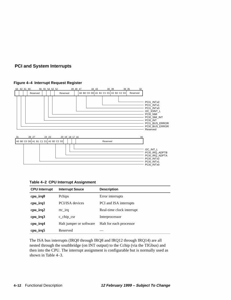
PCI and System Interrupts
Figure 4–4 Interrupt Request Register
The ISA bus interrupts (IRQ0 through IRQ8 and IRQ12 through IRQ14) are all nested through the southbridge (on INT output) to the Cchip (via the TIGbus) and then into the CPU. The interrupt assignment is configurable but is normally used as shown in Table 4–3.
Table 4–2 CPU Interrupt Assignment
CPU Interrupt Interrupt Souce Description
cpu_irq0 Pchips Error interrupts
cpu_irq1 PCI/ISA devices PCI and ISA interrupts
cpu_irq2 rtc_irq Real-time clock interrupt
cpu_irq3 c_chip_csr Interprocessor
cpu_irq4 Halt jumper or software Halt for each processor
cpu_irq5 Reserved —
63 55 54 53 52 48 47 44 43 40 39
24 23
35
20
36 32
31 28
ReservedC2 D2B2A2C1 D1B1A1C0 D0B0A0
PCI1_INTx2PCI1_INTx1PCI1_INTx0I2C_IOINT_LPCI0_NMIPCI0_SMI_INTPCI0_INTPCI1_BUS_ERRORPCI0_BUS_ERRORReserved
I2C_INT_LPCI0_IRQ_ADPTBPCI0_IRQ_ADPTAPCI0_INTx2PCI0_INTx1PCI0_INTx0
27 00
62 61 60 56
19 18 17
Reserved Reserved
ReservedC2 D2B2A2C1 D1B1A1C0 D0B0A0
49
16
4–12 Functional Description 12 February 1999 – Subject To Change

ISA Devices
The AlphaPC 264DP timer interrupt is generated by the real-time clock by means of the square-wave output of the southbridge chip, which routes the interrupt directly to the Cchip.
4.8 ISA Devices
The following section describes the AlphaPC 264DP ISA bus implementation with peripheral devices and connectors.
Table 4–3 ISA Interrupts
Interrupt Level Interrupt Source
Interrupt Level Interrupt Source
IRQ0 Interval timer IRQ8 Reserved
IRQ1 Keyboard IRQ9 16-bit ISA
IRQ2 Chains interrupt from slave peripheral interrupt controller
IRQ10 16-bit ISA
IRQ3 8-bit ISA (COM2) IRQ11 16-bit ISA
IRQ4 8-bit ISA (COM1) IRQ12 Mouse
IRQ5 8-bit ISA (parallel port) IRQ13 16-bit ISA
IRQ6 8-bit ISA (floppy disk) IRQ14 16-bit ISA
IRQ7 8-bit ISA (parallel port) IRQ15 IDE
12 February 1999 – Subject To Change Functional Description 4–13

DC Power Distribution
. The
unc-ents s.
A
r s can stan-
-pin n the
-
ed
ply.
oard logic is- con-
4.8.1 Super I/O Controller
The AlphaPC 264DP uses the SMC FDC37C669 as the combination controller chip (see Table 2–1 and Figure 2–1). It is packaged in a 100-pin PQFP configurationchip provides the following ISA peripheral functions:
• Diskette controller – Software compatible with the Intel PC8477 (contains asuperset of the Intel DP8473 and NEC PD765 and the Intel N82077 FDC ftions). The onchip analog data separator requires no external filter componand supports the 4Mb drive format and 5.25-inch and 3.5-inch diskette driveFDC data and control lines are brought out to a standard 34-pin connector.ribbon cable interfaces the connector to one or two diskette drives.
• Serial ports – Two UARTs with modem control, compatible with NS16450 oPC16550, are brought out to separate onboard, 10-pin connectors. The linebe brought out through 9-pin female D-sub connectors on the bulkhead of adard PC enclosure.
• Parallel port – The bidirectional parallel port is brought out to an onboard 25connector. It can be brought out through a 25-pin female D-sub connector obulkhead of a standard PC enclosure.
Refer to the SMC FDC37C669 specification for further information (including timing, electrical characteristics, and mechanical data).
4.8.2 ISA Expansion Slot
One ISA expansion slot is provided for plug-in ISA peripherals. This slot is sharwith the PCI and can be used for a PCI or ISA device.
4.9 DC Power Distribution
The AlphaPC 264DP derives its system power from a user-supplied power supThe power supply must provide +12 V dc, −12 V dc, −5 V dc, +5 V dc, 5VSB dc and 3.3 V dc. The dc power is supplied through two power connectors on the mainb(J3 and J33) and one on the daughtercard (J4). Power is distributed to the boardthrough dedicated power planes within the 12-layer board structure. Power is dtributed to the daughtercard through the connector and dedicated 18-pin powernector from the power supply.
4–14 Functional Description 12 February 1999 – Subject To Change

DC Power Distribution
3. The
d to
Ms, rmi-
upply The n-
Figure 4–5 shows that the +12 V dc, −12 V dc, +5 V dc, and −5 V dc are supplied to ISA connector J47. The +12 V dc and −12 V dc are supplied to the PCI connectorsJ35, J40–42, J44, and J46, and to the two daughtercard connectors J18 and J2+12 V dc is also supplied to the fan box connectors J2, J15, J22, and J24.
In addition to the ISA connector, +5.0 V dc is supplied to the PCI connectors anmost of the board’s integrated circuits.
The +3.3 V dc is provided to the PCI slots, the 21272 core logic chipset, the DIMthe daughtercard connectors, and the linear regulator that provides the 2.0-V tenation voltage to the mainboard and the daughtercard connectors.
The power supply also provides 5 VSB to the comm port (J19) and soft power.
Figure 4–5 also shows that the daughtercard receives +5 V dc from the power sand distributes it to the dc-to-dc converter and miscellaneous logic on the card.daughtercard edge connector (J3) provides the following voltages from the maiboard:
• +3.3 V for the SSRAMs, miscellaneous logic on the card, and for the linear reg-ulator for conversion to 1.5 V for SSRAM I/O
• +12 V for fan power and RS-232 logic
• –12 V for RS-232 logic
• +2.0 V for termination logic
12 February 1999 – Subject To Change Functional Description 4–15

Reset and Initialization
Figure 4–5 AlphaPC 264DP Power Distribution
4.10 Reset and Initialization
This logic is contained on the daughtercard in a Quicklogic QL12X16BL FPGA. This controls reset, power OK, SROM test port, and interrupts to the CPU.
The TIGbus FPGA will implement system irq, general configuration registers, and Motorola synthesizer setup based on CPU speed and 21272 speed. It will also pro-vide the interface to the flash ROM.
+2.2 V
−12 V
+5 V
−5 V
+12 V
+3.3 V
15
1, 3, 5, 7,10, 12, 14
24
1, 3, 5, 7,9, 11, 14,16, 18, 20
12
PCI32 Conn.
Spkr Conn.
IntegratedCircuits/Clocks
21272
LinearRegulator
J33
DIMMs
ISA Conn.Fans
Comm.Port
J3
16
Daughter-card
Conn.J3
+5VSB
Mainboard
Daughtercard+5 V
1, 3, 5, 7,9, 11, 13,15, 17
J4
+2.0 V
dc-to-dcConverter 21264
SSRAMs
MISC
−12 V
+12 V
+2.0 V
+3.3 V
FansRS-232SSRAM
I/O
1-8, 91-98
86
176
87-90,177-180
Termination
TerminationLinear
Regulator
+1.5 V
Comm.Port
MISC
MISC
4–16 Functional Description 12 February 1999 – Subject To Change
System Software
4.11 System Software
The AlphaPC 264DP software is divided into the following categories:
• Serial ROM code
• Flash ROM code
• Operating systems
4.11.1 Serial ROM Code
The serial ROM code is contained in a 512KB flash ROM. The serial ROM code ini-tializes the system, which includes loading Debug Monitor or other code from the flash ROM. The serial ROM code then transfers control to the code loaded from the flash ROM.
The Mini-Debugger is also resident in the SROM. Switch 4 can be set on SW2 (see Section 2.2) for CPU0 and CPU1 to trap to the Mini-Debugger. Connector J2 on the daughtercard provides a terminal port for the Mini-Debugger.
4.11.2 Flash ROM Code
The AlphaPC 264DP includes an industry-standard, 2MB flash ROM – AMD AM29F016.
4.11.3 Operating Systems
The AlphaPC 264DP is designed to run Windows NT and Tru64 UNIX.
12 February 1999 – Subject To Change Functional Description 4–17


Memory Subsystem
an pu-s
5System Memory and Address Mapping
5.1 Memory Subsystem
The DRAM memory subsystem on the AlphaPC 264DP consists of sixteen 200-pin buffered DIMM slots, which are organized as four arrays of memory. The 21272 chipset supports two 256-bit memory buses (288-bit including ECC) with two arrays on each bus (see Figure 5–1).
The 72-bit, 100-MHz DIMMs consist of 64 bits of data and 8 bits of ECC, and cbe 32MB, 64MB, 128MB, or 256MB. The minimum configuration (one array polated with four 32MB DIMMs) is 128MB. The maximum configuation (four arrayeach populated with four 256MB DIMMs) is 4GB.
The memory cycle time is 83 MHz, identical to the 21272 chipset cycle time.
Note: Although the memory cycle time is 83 MHz, qualified 100-MHz DIMMs are required.
Figure 5–1 AlphaPC 264DP Memory Subsystem
Data Bus 1
Data Bus 0
2127221264
Dchips
PchipsArray 3Array 1Array 2Array 0
Cchip
Address/Control
12 February 1999 – Subject To Change System Memory and Address Mapping 5–1
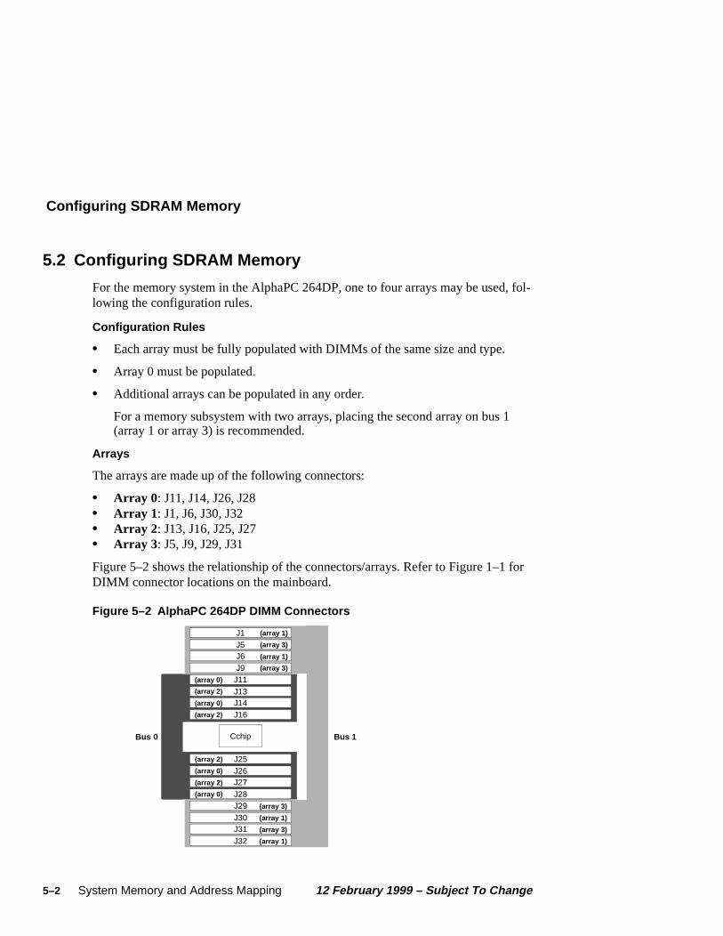
Configuring SDRAM Memory
for
5.2 Configuring SDRAM Memory
For the memory system in the AlphaPC 264DP, one to four arrays may be used, fol-lowing the configuration rules.
Configuration Rules
• Each array must be fully populated with DIMMs of the same size and type.
• Array 0 must be populated.
• Additional arrays can be populated in any order.
For a memory subsystem with two arrays, placing the second array on bus 1 (array 1 or array 3) is recommended.
Arrays
The arrays are made up of the following connectors:
• Array 0: J11, J14, J26, J28• Array 1: J1, J6, J30, J32• Array 2: J13, J16, J25, J27• Array 3: J5, J9, J29, J31
Figure 5–2 shows the relationship of the connectors/arrays. Refer to Figure 1–1DIMM connector locations on the mainboard.
Figure 5–2 AlphaPC 264DP DIMM Connectors
J1
J5J6J9J11
J13J14J16
J25J26J27
J28J29J30J31J32
CchipBus 0 Bus 1
(array 2)
(array 0)
(array 2)
(array 0)
(array 0)
(array 2)
(array 0)
(array 2)
(array 1)
(array 3)
(array 1)
(array 3)
(array 3)
(array 1)
(array 3)
(array 1)
5–2 System Memory and Address Mapping 12 February 1999 – Subject To Change
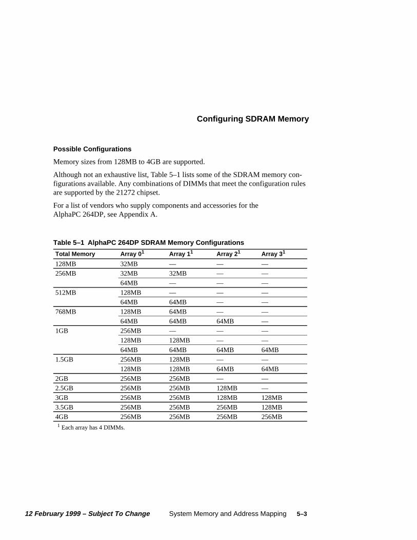
Configuring SDRAM Memory
n-les
Possible Configurations
Memory sizes from 128MB to 4GB are supported.
Although not an exhaustive list, Table 5–1 lists some of the SDRAM memory cofigurations available. Any combinations of DIMMs that meet the configuration ruare supported by the 21272 chipset.
For a list of vendors who supply components and accessories for the AlphaPC 264DP, see Appendix A.
Table 5–1 AlphaPC 264DP SDRAM Memory Configurations
Total Memory Array 01
1 Each array has 4 DIMMs.
Array 11 Array 21 Array 31
128MB 32MB — — —
256MB 32MB 32MB — —
64MB — — —
512MB 128MB — — —
64MB 64MB — —
768MB 128MB 64MB — —
64MB 64MB 64MB —
1GB 256MB — — —
128MB 128MB — —
64MB 64MB 64MB 64MB
1.5GB 256MB 128MB — —
128MB 128MB 64MB 64MB
2GB 256MB 256MB — —
2.5GB 256MB 256MB 128MB —
3GB 256MB 256MB 128MB 128MB
3.5GB 256MB 256MB 256MB 128MB
4GB 256MB 256MB 256MB 256MB
12 February 1999 – Subject To Change System Memory and Address Mapping 5–3

System Address Mapping
5.3 System Address Mapping
This section describes the mapping of the processor physical address space into memory and I/O space addresses. It also includes the translations of the processor-initiated address into a PCI address, and PCI-initiated addresses into physical mem-ory addresses.
5.3.1 CPU Address Mapping to PCI Space
The physical sysbus address space is composed of the following:
• Memory address space
• Local I/O space, for registers residing on the sysbus (that is, registers in the Cchip, Dchips, and Pchips)
• PCI space
The PCI defines four physical address spaces, as follows:
• PCI memory space (for memory residing on the PCI)
• PCI I/O space
• PCI configuration space
• PCI interrupt acknowledge cycles /PCI special cycles
Refer to the 21272 functional specification for details in this area.
5.3.2 TIGbus Address Mapping
Table 5–2 shows the address map for the TIGbus.
Table 5–2 TIGbus Address Mapping
capbus[23:21]
Physical Address Access Function Comment
000 801 00xx xxx0 (2MB)
RW Flash ROM address space —
001 801 08xx xxx0 RO Gpen_0 Array0_PD[7:0] Reserved
010 801 10xx xxx0 RO Gpen_1 Array1_PD[7:0] Reserved
011 801 18xx xxx0 RO Gpen_2 Array2_PD[7:0] Reserved
100 801 20xx xxx0 RO Gpen_3 Array3_PD[7:0] Reserved
5–4 System Memory and Address Mapping 12 February 1999 – Subject To Change
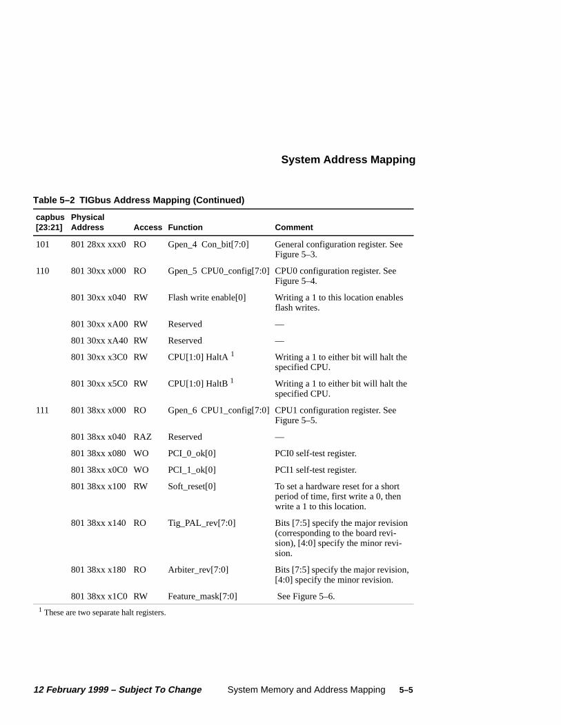
System Address Mapping
s
t
,
101 801 28xx xxx0 RO Gpen_4 Con_bit[7:0] General configuration register. See Figure 5–3.
110 801 30xx x000 RO Gpen_5 CPU0_config[7:0] CPU0 configuration register. SeeFigure 5–4.
801 30xx x040 RW Flash write enable[0] Writing a 1 to this location enableflash writes.
801 30xx xA00 RW Reserved —
801 30xx xA40 RW Reserved —
801 30xx x3C0 RW CPU[1:0] HaltA 1 Writing a 1 to either bit will halt the specified CPU.
801 30xx x5C0 RW CPU[1:0] HaltB 1 Writing a 1 to either bit will halt the specified CPU.
111 801 38xx x000 RO Gpen_6 CPU1_config[7:0] CPU1 configuration register. SeeFigure 5–5.
801 38xx x040 RAZ Reserved —
801 38xx x080 WO PCI_0_ok[0] PCI0 self-test register.
801 38xx x0C0 WO PCI_1_ok[0] PCI1 self-test register.
801 38xx x100 RW Soft_reset[0] To set a hardware reset for a shorperiod of time, first write a 0, then write a 1 to this location.
801 38xx x140 RO Tig_PAL_rev[7:0] Bits [7:5] specify the major revision(corresponding to the board revi-sion), [4:0] specify the minor revi-sion.
801 38xx x180 RO Arbiter_rev[7:0] Bits [7:5] specify the major revision[4:0] specify the minor revision.
801 38xx x1C0 RW Feature_mask[7:0] See Figure 5–6.1 These are two separate halt registers.
Table 5–2 TIGbus Address Mapping (Continued)
capbus[23:21]
Physical Address Access Function Comment
12 February 1999 – Subject To Change System Memory and Address Mapping 5–5

System Address Mapping
’s
onfig-
onfig-
hip’s
The Gpen4 register, shown in Figure 5–3, reflects the settings of the mainboardswitchpack 2 (see Figure 2–3).
Figure 5–3 Gpen4 Register
The Gpen5 register, shown in Figure 5–4, shows the CPU speed and Bcache curation (set by onboard resistors) on the daughtercard containing CPU0.
Figure 5–4 Gpen5 Register
The Gpen6 register, shown in Figure 5–5, shows the CPU speed and Bcache curation (set by onboard resistors) on the daughtercard containing CPU1.
Figure 5–5 Gpen6 Register
The feature mask register, shown in Figure 5–6, allows you to set the Cypress carbiter activity.
Figure 5–6 Feature Mask Register
7 6 5 4 3 2 1 0
FSBReservedMini-Debugger21272 sp[2:0]AlphaBIOS password bypass
7 6 5 4 3 2 1 0
cpu0_speed[2:0]bc0_config[3:0]cpu0_present_l
7 6 5 4 3 2 1 0
cpu1_speed[2:0]bc1_config[3:0]cpu1_present_l
7 6 5 4 3 2 1 0
Arbiter select.
0 Selects the arbiter that deasserts the Cypress chip’s grant after it claims the transaction.
1 Selects the arbiter that holds the assertion of the Cypress chip’s grant until it has deasserted its request.
RAZ
5–6 System Memory and Address Mapping 12 February 1999 – Subject To Change

ASupport, Products, and Documentation
A.1 Customer Support
Alpha OEM provides the following web page resources for customer support.
URL Description
http://www.digital.com/alphaoem Contains the following links:
• Developers’ Area: Development tools, code examples, driver developers’ information, and technical white papers
• Motherboard Products: Motherboard details and performance information
• Microprocessor Products: Microprocessor details and performance information
• News: Press releases
• Technical Information: Motherboard firmware and drivers, hardware compatibility lists, and product documentation library
• Customer Support: Feedback form
12 February 1999 – Subject to Change Support, Products, and Documentation A–1

Supporting Products
A.2 Supporting Products
This section lists sources for components and accessories that are not included with the AlphaPC 264DP.
A.2.1 Memory
Dual inline memory modules (DIMMs) are available from a variety of vendors. For a list of the qualified vendors, visit the Alpha OEM World Wide Web Internet site at URL:
http://www.digital.com/alphaoem
Click on Technical Information. Then click on Alpha OEM Hardware Compatibility List.
A.2.2 Power Supply
A power supply, suitable for use with the AlphaPC 264DP (+3.3 V, +5 V, –5 V, +12 V, –12 V), is available from:
Antec, Inc.
2859 Bayview DriveFremont, CA 94538Phone: 510–770–1200, ext. 312PN PRS-618 (630 W)
A.2.3 Enclosure
An enclosure, suitable for housing the AlphaPC 264DP and its power supply, isavailable from:
Delta Axxion Technology
1550 NorthwesternEl Paso, TX 79912Phone: 915–877–5288PN TL-22
A–2 Support, Products, and Documentation 12 February 1999 – Subject to Change
Alpha Products
hard-
A.3 Alpha Products
To order the AlphaPC 264DP mainboard, contact your local sales office. The follow-ing tables list some of the Alpha products available.
Note: The following products and order numbers might have been revised. For the latest versions, contact your local sales office.
Motherboard kits include the mainboard and user’s manual.
Design kits include documentation and schematics. They do not include relatedware.
Chips Order Number
Alpha 21264 microprocessor (500 MHz) 21264–A1
Motherboard Kits Order Number
AlphaPC 264DP Dual Processor Planar Board 21A06–B0
AlphaPC 264DP 500-MHz CPU Board with 2MB Cache 21A06–M0
AlphaPC 264DP 500-MHz CPU Board with 4MB Cache 21A06–M1
Design Kits Order Number
Alpha Motherboards Software Developer’s Kit QR–21B02–04
12 February 1999 – Subject to Change Support, Products, and Documentation A–3
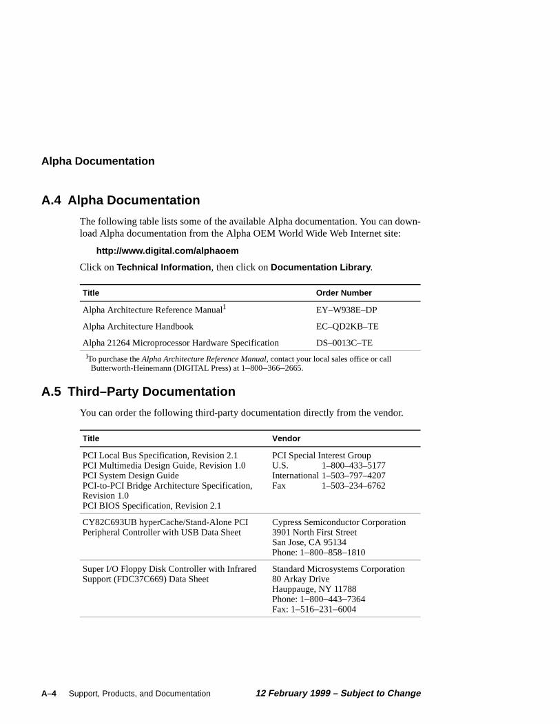
Alpha Documentation
A.4 Alpha Documentation
The following table lists some of the available Alpha documentation. You can down-load Alpha documentation from the Alpha OEM World Wide Web Internet site:
http://www.digital.com/alphaoem
Click on Technical Information, then click on Documentation Library.
A.5 Third–Party Documentation
You can order the following third-party documentation directly from the vendor.
Title Order Number
Alpha Architecture Reference Manual1
1To purchase the Alpha Architecture Reference Manual, contact your local sales office or call Butterworth-Heinemann (DIGITAL Press) at 1–800–366–2665.
EY–W938E–DP
Alpha Architecture Handbook EC–QD2KB–TE
Alpha 21264 Microprocessor Hardware Specification DS–0013C–TE
Title Vendor
PCI Local Bus Specification, Revision 2.1PCI Multimedia Design Guide, Revision 1.0PCI System Design GuidePCI-to-PCI Bridge Architecture Specification,Revision 1.0PCI BIOS Specification, Revision 2.1
PCI Special Interest GroupU.S. 1–800–433–5177International 1–503–797–4207Fax 1–503–234–6762
CY82C693UB hyperCache/Stand-Alone PCI Peripheral Controller with USB Data Sheet
Cypress Semiconductor Corporation 3901 North First StreetSan Jose, CA 95134Phone: 1–800–858–1810
Super I/O Floppy Disk Controller with Infrared Support (FDC37C669) Data Sheet
Standard Microsystems Corporation80 Arkay DriveHauppauge, NY 11788Phone: 1–800–443–7364Fax: 1–516–231–6004
A–4 Support, Products, and Documentation 12 February 1999 – Subject to Change

Index
A Connector specifications
Abbreviations, x
Address decode, 4-2
Address mappingsystem, 5-4TIGbus, 5-4
Alpha products, A-3
AlphaPC, 2-9
BBit notation, xi
Block diagram, 1-2
Busmemdata, 4-5padbus, 4-5sysdata, 4-4
CCchip, 1-3
functional overview, 4-2Clock subsystem, 1-4, 4-7
distribution, 4-8Combination controller, 1-5, 4-14
Configuration rules, 5-2
Configuration switchesdaughtercard, 2-8 to 2-9mainboard, 2-5 to 2-8
mainboard, 3-4Connectors
daughtercard, 2-4, 2-5mainboard, 2-2, 2-3pinouts
daughtercard, 2-22 to 2-24mainboard, 2-9 to 2-21
Controllercombination, 1-5, 4-14memory, 4-3super I/O, 1-5, 4-14
Conventionsnumbering, xii
Core logic chipset, 1-2Cchip, 1-3, 4-2Dchip, 1-3, 4-4introduction, 4-1Pchip, 1-3, 4-6speed, 2-8
CPU interface, 4-2
DData field size, xi
Data units, xi
12 February 1999 – Subject to Change Index–1

Daughtercardconfiguration switches, 2-8 to 2-9connector pinouts, 2-22 to 2-24dc-to-dc converter, 1-4dimensions, 3-2environmental requirements, 3-2hole specifications, 3-6level 2 cache, 1-4overview, 1-3power requirements, 3-1switch/connector/component list, 2-5switch/connector/component location, 2-4
Dchip, 1-3functional overview, 4-4
dc-to-dc converterdaughtercard, 1-4
Dimensionsdaughtercard, 3-2mainboard, 3-2
DocumentationAlpha, A-4third party, A-4
EEnvironmental requirements, 3-2
Extents and ranges, xii
FFail-safe booter, 2-7
Flash write protection, 2-8
FSB, 2-7
Functional block diagram, 1-2
HHole specifications
daughtercard, 3-6mainboard, 3-3
II/O specifications
mainboard, 3-5IDE interface, 1-5
Interrupt request register, 4-12
Interrupts, 4-11
INTnn, xi
ISAdevices, 4-13slot, 1-5, 4-14
MMainboard
configuration switches, 2-5 to 2-8connector pinouts, 2-9 to 2-21connector specifications, 3-4dimensions, 3-2environmental requirements, 3-2hole specifications, 3-3I/O specifications, 3-5power requirements, 3-1switch/connector/component list, 2-3switch/connector/component location, 2-2
Memdata bus, 4-5
Memoryconfiguration rules, 5-2configurations, 5-3organization, 4-3subsystem, 1-2, 5-1timing, 2-7vendors, A-2
Memory controller, 4-3
Memory products, A-2
Memory subsystem, 5-1organization, 4-3
Mini-Debugger, 2-7
NNumbering convention, xii
Index–2 12 February 1999 – Subject to Change
OOperating systems, 4-17
Ordering products and documentation, A-3
PPadbus, 4-5
Password bypass, 2-7
Pchip, 1-3functional overview, 4-6
PCIarbitration, 4-10devices, 4-8interface, 1-5, 4-6interrupts, 4-11
Powerdistribution, 4-14, 4-16requirements, 3-1
Power connectorsdaughtercard, 2-24fan box, 2-19mainboard, 2-19
ProductsAlpha, A-3enclosure, A-2memory, A-2power supply, A-2
RRanges and extents, xii
Registerinterrupt request, 4-12
Requirementsenvironmental, 3-2physical, 3-2power, 3-1
ROdefinition, x
RWdefinition, x
SSCSI interface, 1-5, 4-10
Southbridge, 1-5, 4-9
Super I/O controller, 1-5, 4-14
Supporttechnical, A-1
Switches, See Configuration switches
Sysdata bus, 4-4
System address mapping, 5-4
System interrupts, 4-11
System software, 4-17
TTIGbus address mapping, 5-4
UUNDEFINED
definition, xiiiUNPREDICTABLE
definition, xiii
WWO
definition, x
12 February 1999 – Subject to Change Index–3