AGNOSTIC VALIDATION TEST BENCH FOR EFUSE …eprints.usm.my/38350/1/CHAN_WEI_JIAN_24_Pages.pdf ·...
34
AGNOSTIC VALIDATION TEST BENCH FOR EFUSE CONNECTIVITY VERIFICATION By CHAN WEI JIAN A Dissertation submitted for partial fulfilment of the requirement for the degree of Master of Science (Microelectronic Engineering) August 2017
Transcript of AGNOSTIC VALIDATION TEST BENCH FOR EFUSE …eprints.usm.my/38350/1/CHAN_WEI_JIAN_24_Pages.pdf ·...

AGNOSTIC VALIDATION TEST BENCH FOR EFUSE
CONNECTIVITY VERIFICATION
By
CHAN WEI JIAN
A Dissertation submitted for partial fulfilment of the requirement for
the degree of Master of Science (Microelectronic Engineering)
August 2017

Acknowledgement
This research has given me an opportunity to strengthen my technical depth in validation
field which helps me to perform better in my daily work and advance in my career.
Throughout this research, I’ve learnt to think out of the box, be innovative and creative in
resolving problems. The whole process was challenging but it was very fruitful and
worthwhile. The skillset that I’ve obtained will be useful not just in work, but in non-work
related things as well. I would like to express my gratitude to all USM engineering staff
for this great opportunity to participate in this Master research program.
Secondly, I owe a deep sense of gratitude to my supervisor, Dr. Nur Zatil 'Ismah Hashim,
for her kindness guidance and timely suggestion to every stage of my research. Her
dedication, prompt response for all my queries, and detail oriented attitude towards my
work has motivated me to strive for perfection and enable me to complete my thesis.
Thanks again to Dr. Zatil for all the helps and suggestions provided.
Lastly, I would like to thank profusely to all colleagues and friends in my work place who
have helped me in my research. They have provided useful suggestion on technical issues
such as coding syntax and methodology that I’ve encountered throughout my work. This
allows me to proceed further and accomplish my task.

Table of Content
LIST OF FIGURES ............................................................................................................. I
LIST OF TABLES .............................................................................................................III
LIST OF ABBREVIATIONS ........................................................................................... IV
ABSTRAK .......................................................................................................................... V
ABSTRACT ...................................................................................................................... VI
CHAPTER 1: INTRODUCTION ........................................................................................1
1.1 Overview ....................................................................................................................1 1.2 Problem Statement .....................................................................................................3
1.3 Aim and Objectives ...................................................................................................5 1.4 Scope of Work ...........................................................................................................6
1.5 Thesis Outline ............................................................................................................6
CHAPTER 2: LITERATURE REVIEW .............................................................................8 2.1 Verification Environment ..........................................................................................9
2.2 Device Under Test ...................................................................................................11 2.3 Semiconductor IP Block: .........................................................................................11
2.4 CPU & PCH Architecture ........................................................................................12 2.5 eFUSE Technology ..................................................................................................15
2.5.1 Evolution from Laser Fuse to Electric Fuse (Robson N. et al., 2007) ............17
2.6 Register Space ..........................................................................................................22
2.6.1 PCI Configuration Space .................................................................................23 2.6.2 PCI Memory and I/O Space ............................................................................25
2.7 Intel On Chip System Fabric (IOSF) Interface: .......................................................27
2.7.1 IOSF Primary Interface ...................................................................................30 2.7.2 IOSF Sideband Interface .................................................................................32
2.8 Current eFUSE Connectivity Validation Flow ........................................................34 2.8.1 Current Verification Method and eFUSE Connectivity Test Structure ...........36
2.9 Summary ..................................................................................................................38
CHAPTER 3: METHODOLOGY .....................................................................................39 3.1 Overall Research Work Flow ..................................................................................40
3.2 New eFUSE Connectivity Validation Flow .............................................................43 3.2.1 New Verification Method and eFUSE Connectivity Test Structure ...............45 3.2.2 Perl Script Format for Test Generation ...........................................................48 3.2.3 Perl Script Code Overview ..............................................................................51
3.3 Summary ..................................................................................................................56
CHAPTER 4: RESULTS AND DISCUSSIONS ..............................................................57 4.1 Results and Observation from The New eFUSE Validation Flow ..........................58
4.1.1 Validation Efficiency .......................................................................................58

4.1.2 Simulation Time ..............................................................................................61
4.1.3 eFUSE Coverage .............................................................................................65 4.2 Perl Script Discussion ..............................................................................................68
4.2.1 Automated Flow to Detect Overridden eFUSE in Verification Environment
..........................................................................................................................68 4.2.2 Automated SoC Path Discovery and Append. ................................................69
4.3 Summary ..................................................................................................................71
CHAPTER 5: CONCLUSION AND FUTURE WORK ...................................................72 5.1 Conclusion ...............................................................................................................72
5.2 Recommendation for Future Work ..........................................................................73
REFERENCES ..................................................................................................................74

I
List of Figures
Figure 2.1: OVM verification environment (Cadence Design Systems Inc, 2011) .......... 10
Figure 2.2: CPU, Northbridge and Southbridge connectivity (Laan S., 2015) ................. 13
Figure 2.3: CPU and PCH connectivity (Laan S., 2015) .................................................. 14
Figure 2.4: eFUSE connection and distribution diagram.................................................. 17
Figure 2.5: PCI Configuration space (Rusling, 1999) ...................................................... 25
Figure 2.6: Base address format for Memory and I/O space (Rusling, 1999) .................. 27
Figure 2.7: IOSF interface (US Patent No. US20140258583, 2014)................................ 30
Figure 2.8: IOSF primary interface (US Patent No. US20140258583, 2014) .................. 31
Figure 2.9: Avoton's south complex IOSF interconnects (Wasson, 2013) ....................... 32
Figure 2.10: IOSF sideband interface (US Patent No. US20140258583, 2014) .............. 33
Figure 2.11: Existing eFUSE validation flow chart .......................................................... 35
Figure 2.12: Front door read access method ..................................................................... 37
Figure 2.13: eFUSE connectivity test developed for individual IP .................................. 38
Figure 3.1: Research flow chart ........................................................................................ 42
Figure 3.2: New eFUSE validation flow chart.................................................................. 44
Figure 3.3: Backdoor read access method ........................................................................ 45
Figure 3.4: eFUSE hierarchical information example ...................................................... 47
Figure 3.5: eFUSE connectivity test is generated and consolidated ................................. 48
Figure 3.6: Perl Script input and output ............................................................................ 50
Figure 3.7: Main body of the Perl script ........................................................................... 51
Figure 3.8: parse_cmd_line subroutine ............................................................................. 52
Figure 3.9: read_rules_file subroutine .............................................................................. 53
Figure 3.10: parse_eFUSE subroutine .............................................................................. 54

II
Figure 3.11: generate_test subroutine ............................................................................... 55
Figure 3.12: eFUSE test template ..................................................................................... 56
Figure 4.1: Overall eFUSE validation flow improvement ................................................ 61
Figure 4.2: Total simulation time using previous eFUSE verification method for 5 IPs . 63
Figure 4.3: Total simulation time using new eFUSE verification method ....................... 64
Figure 4.4: eFUSE coverage comparison for 5 selected IPs ............................................. 67
Figure 4.5: SoC & IP Hierarchy ....................................................................................... 70

III
List of Tables
Table 4.1: Efficiency improvement in test development flow .......................................... 59
Table 4.2: Efficiency improvement in overall eFUSE connectivity validation flow ....... 60
Table 4.3: Average simulation time for old and new eFUSE connectivity test ................ 64
Table 4.4: Coverage improvement .................................................................................... 67

IV
List of Abbreviations
Abbreviation
API
BIOS
CPU
CRP
DFD
DFT
DMI
DUT
ECAM
eFUSE
EUT
FSB
IO
IOSF
IP
ISA
MMIO
NMOS FET
NVRAM
OVC
OVM
PCH
PCI
PUF
RAM
RTL
SATA
SoC
TTM
USB
UUT
VLSI
Meaning
Application Program Interface
Basic Input Output System
Central Processing Unit
Challenge Response Pair
Design for Debug
Design for Test
Direct Media Interface
Device Under Test
Enhanced Configuration Access Mechanism
Electronic Fuse / Electric Fuse
Equipment Under Test
Front Side Bus
Input Output
Integrated On Chip System Fabric / Intel On Chip System Fabric
Intellectual Property
Industrial Standard Architecture
Memory Mapped I/O
N-type MOSFET
Non-Volatile RAM
OVM Verification Component
Open Verification Methodology
Platform Controller Hub
Peripheral Component Interconnect
Physical Unclonable Function
Random Access Memory
Register-Transfer Level
Serial ATA
System On Chip
Time To Market
Universal Serial Bus
Unit Under Test
Very Large Scale Integration

V
Model Pengesahan Agnostik untuk Pengujian Sambungan eFUSE
ABSTRAK
Dalam industri semikonduktor, proses pengesahan adalah penting untuk mencari kesilapan
reka bentuk dan membetulkannya sebelum produk dilancarkan. Litar bersepadu
semikonduktor biasanya akan diperbaharui dalam kitaran tahunan. Oleh sebab ini, kitaran
reka bentuk dan pengesahan yang singkat perlu diutamakan tanpa mengabaikan kualiti
produk. Pada masa kini, proses pengesahan litar bersepadu sering menjadi satu faktor yang
melambatkan kesediaan produk. Proses pengesahan litar bersepadu perlu diperbaiki supaya
ia seiring dengan kemajuan proses reka bentuk litar bersepadu. Dalam kerja ini,
penambahbaikan pengesahan sambungan eFUSE (Electrik FUSE) proses akan difokus.
eFUSE merupakan satu ciri yang terdapat dalam litar bersepadu. Ia berfungsi sebagai pusat
penyimpanan ‘tetapan’ penting litar bersepadu dan ‘tetapan’ tersebut akan diagihkan ke
setiap harta intelek semasa permulaan operasi system komputer. Pengesahan sambungan
eFUSE diperlukan untuk memastikan setiap harta intelek mendapat nilai eFUSE yang
betul. Dalam kerja ini, konsep model pengesahan sambungan eFUSE agnostik akan
diwujudkan dan diuji. Ideanya adalah untuk menghapuskan penjanaan kod ujian secara
manual, menambah kecekapan pengujian serta membolehkan pengunaan semula kod ujian
dalam projek yang berbeza. Kaedah ini dapat mengurangkan tempoh masa pengesahan
sambungan eFUSE secara ketara, iaitu sebanyak 28%. Purata penambahbaikan peratus
liputan eFUSE adalah sebanyak 65%. Kesimpulannya, tempoh masa pengesahan
sambungan eFUSE dapat dikurangkan tanpa mengorbankan kualiti ujian.

VI
Agnostic Validation Test Bench for eFUSE Connectivity Verification
ABSTRACT
In semiconductor industry, validation is an important process to discover design bugs and
have it fixed before the product is released. Semiconductor integrated circuit is normally
refreshed in yearly cadence and it is crucial to have a short design and validation cycle,
without compromising the product quality. Nowadays, validation process often becomes
the bottleneck for product readiness. Integrated circuit validation flow has to be improved
in order to keep up with the advancement of integrated circuit design flow. In this work,
an improvement method on validation flow is discussed, with particular focus on eFUSE
(Electric FUSE) connectivity validation. eFUSE is a feature available in integrated circuit
which functions as a central storage for important ‘settings’, and distribute them during
system boot up process. eFUSE connectivity validation is needed to ensure each
intellectual property is able to retrieve the correct eFUSE value. In this work, the concept
of agnostic validation test bench for eFUSE connectivity validation is developed and tested
the idea of it is to eliminate manual test development effort, improves validation efficiency
and promotes reusability across different projects. By using this methodology, eFUSE
connectivity validation time is reduced significantly and recorded an improvement of 28%.
There is also an average improvement of 65% in eFUSE coverage percentage. In summary,
the eFUSE connectivity validation time frame is shortened, without compromising the test
quality.

1
CHAPTER 1
INTRODUCTION
1.1 Overview
Every semiconductor Central Processing Unit (CPU), chipset or System-on-Chip (SoC)
product requires multiple stages of validation or verification work to be done before it is
launched to the market. There is a pre-silicon validation which involves testing the chip
design using sophisticated simulation and emulation tool to discover functionality bugs.
After the chip is fabricated, it will then have to go through post-silicon validation where
the chip is being tested using actual use case scenario. Post silicon normally serves as a
safety net to discover corner case functionality bugs where pre-silicon failed to catch. In
addition to those, there are also electrical validation and performance validation to ensure
that the chip is able to meet all the requirements mentioned inside the specification
document. All of these validation processes serve only one purpose and that is to
materialise as many design flaws as possible before the products reach the customers or
end users. There will not be a complete product without going through stages of validation.
Hence, this shows that validation plays an important role in semiconductor integrated
circuit industry.

2
In the 21st century, innovations in user interface design are causing a revolution in design
which drives the semiconductor industry to integrate ever-greater system complexity onto
a single chip. The rise in design complexity is motivated by consumer demand for higher
performance products as well as increase in integration density which allow more
functionalities to be placed on a single chip. Today, a leading edge mobile-enabled
electronic system is based on a SoC that contains more than a billion gates, with at least
ten interface protocols, hundreds of Intellectual Property (IP) blocks, power domains and
clock domains. The register-transfer logic (RTL) could goes up to millions line of codes.
This increase in SoC design complexity has created orders of magnitude greater
challenges in SoC verification or validation. In addition, there is a strong urge to verify
variety of scenarios such as power management, device-level software, analog
components, low power structural checks and many more (Lipon, 2014). All this
additional feature in advance SoC design indirectly creates more validation tasks. Hence,
sheer capacity in verification or validation technology is desperately needed.
Apart from the system complexity, another crucial factor that drives the success of a
semiconductor company is the importance of short design time. Consequently, the amount
of simulation required to design digital systems also increase significantly. Simulation
time typically scales as the square of the increase in system complexity. In order to keep
the design time to a minimum and align it to the product launch date, it is critical to
structure the simulation environment to make it possible to trade-off simulation
performance for model detail in a flexible manner that allows concurrent software and
hardware development (Olukotun K. et al., 1998). It is important to have continuous effort
to improve the simulation environment so that the validation time is kept at the minimum.

3
Short design time is important because after the design is conceived and before the system
is brought to the market, there is a limited time window in preserving its competitive
performance (Olukotun K. et al., 1998).
In summary, design complexity and short design time are the two major challenges that
makes the validation work becomes difficult over the years. As design complexity
increases, it is almost impossible for designer to design a perfect chip with zero bugs.
Hence, the validation work has become extendedly important. Moreover, the short design
time factor also pushes the validation task to its limit because it has to meet the product
time-to-market (TTM) schedule without sacrificing the quality of validation. Verification
is a major obstacle in creating the final product and it is the most important component of
timely market release and success (Sethulekshmi R, et al., 2016). For this reason, there is
a need to improve the validation methodology to ensure that it is aligned with the design
advancement.
1.2 Problem Statement
The integration of more than a million transistors on a single chip has been achieved with
the development of semiconductor manufacturing process of 16 nanometer. The
complexity of this has made verification the most critical bottleneck in the chip design
flow. Approximately 70 to 80 percent of the design cycle is spent on functional
verification. The SoC design faces a gap between the production capabilities and time to
market pressures. The longer a bug of a design does undetected, the more expensive it will
cost when it is discovered. So both innovative verification methodologies and an effective

4
verification environment are urgently needed (Chai L. et al., 2014). Increase in efficiency
of verification, and reduction of time consumed in verification stage are therefore crucial
to speed up the entire development process (Li Y. et al., 2009).
SoC verification scope has been increased to verify IPs’ integration and on-chip inter-IP
communication among multiple IPs (Zhaohui H. et al., 2012). This means, it is an
important charter in SoC design team to ensure the connectivity and inter-IP
communication is linked or connected correctly. Inside a SoC microprocessor, there will
be a dedicated eFUSE controller, which is an IP, to fetch the values or settings from
eFUSE memory and distribute them to respective IPs. In order for a SoC to function with
desired setting, it is important to make sure that every single IP inside a chip gets the
correct values or setting from the eFUSE memory. This is an important technology and
eFUSE has a history of wide use in embedded systems (Uhlmann G. et al., 2008). Hence,
it is necessary to have eFUSE connectivity validation to check the entire eFUSE
distribution flow. This eFUSE connectivity validation validates the data coherency
between the source which is the eFUSE memory, and the destination which is the IP. In
real world, the eFUSE list could be very huge and it could goes up to hundreds or
thousands of values depends on number of IPs inside a chip, or set of functionality that IP
designer wish to control using eFUSE. Creating a test manually to validate every single
eFUSE connectivity would require huge amount of effort and it is prone to human error.

5
1.3 Aim and Objectives
The goal of this research is to create an ideal test suit to minimize human effort, where the
manual test suit modification or configuration can be reduced to a minimum. Hence,
agnostic validation test bench came into the picture where its purpose is to eliminate the
test dependency on projects and improve the overall portability of the tests. In addition,
the aim is also to create a test bench that is re-usable for future chipsets, which promotes
scalability and reusability (Keaveney M. et al., 2008). Efficient reuse can deliver
significant savings in design cost and time if implemented correctly (Wakefield A. &
Mohd B. J. , 2002). The objectives of this research can be break down into two main
subsections:
1. To create a new test suit that is able to minimize human effort, and maximize
reusability across projects which fulfil the concept of agnostic validation test
bench. By this mean, the aim is to reduce test development effort by introduce
automation element into the eFUSE connectivity validation flow and replace the
traditional manual test development method.
2. To provide a comparative study between the previous and new eFUSE
connectivity validation flow in terms of validation efficiency, simulation time and
resource consumed, and eFUSE coverage. Leverage data from the mentioned
measurable parameters to analyse if the new eFUSE connectivity validation flow
is feasible.

6
1.4 Scope of Work
In general, the research work will be carried out in different phases to fulfil the two main
objectives stated in previous section. Included are the high level scope of work of this
research work, which includes what is in scope and will be covered, and also what is out
of scope, restrictions or limitations.
1. This research will focus only on eFUSE connectivity validation flow or
methodology improvement. This research does not cover functionality validation
methodology, latest eFUSE technology or design architecture of eFUSE
controller.
2. All work will be carried out in OVM-based simulation environment and will be
using System Verilog coding language. Test subject or DUT will be based on the
latest available SoC RTL which is in Verilog code.
1.5 Thesis Outline
This thesis consists of 5 main chapters and it is being organized as follows. Chapter one
starts with the introduction of the importance of validation work. It provides an overview
on the major factors that are driving the needs for validation methodology improvement
or breakthrough. This chapter also highlights the problems encountered in a specific
validation chapter which is eFUSE connectivity validation. The research objectives and
the scope of work have been included in details as well.

7
Chapter 2 includes the theoretical background and literature review that are related to this
research. It contains high level information on the eFUSE design and technology, and
validation methodology that is being used in this specific validation chapter, eFUSE
connectivity validation. In addition, this chapter also covers the background knowledge
of tools and simulation environment that is being used in this research.
Chapter 3 outlines the work flow of this research. This chapter includes the proposed
eFUSE connectivity validation methodology which is expected to exhibits more
advantages and benefits as compared to the previous methodology. The differences and
changes between the new and previous methodology will be included. Details on the new
methodology such as the automation script structure and functions will be explained in
this chapter as well.
Chapter 4 highlights the results obtained by using the new eFUSE connectivity validation
methodology. Comparison is being conducted between the new and previous eFUSE
connectivity validation methodology. The results mainly focus on validation efficiency,
simulation time and eFUSE coverage percentage between two methodologies. Overview
of the Perl script codes is also included in this chapter.
Chapter 5 consists of the conclusion and the recommendation for future work. The major
achievement from this research is summarized and highlighted. In addition, it also
provides recommendation on how this validation methodology can be reused across other
connectivity validation chapter.

8
CHAPTER 2
LITERATURE REVIEW
In the previous chapter, the importance of pre and post silicon validation of a
microprocessor have been discussed. In addition, the brief overview of eFUSE
connectivity validation methodology problem is elaborated.
Complementing the previous chapter, this chapter introduces the necessary background
concepts and literature relating to pre silicon simulation, semiconductor intellectual
property, eFUSE technology, and processor internal interconnects. This chapter starts by
reviewing the pre silicon simulation environment, followed by introduction of DUT and
semiconductor IP. After that, the background of eFUSE technology is reviewed by
looking into eFUSE functionality, application and its evolution. In addition, basic
background theory of register access in computer architecture will be discussed. Finally,
the internal interconnects between of a processor is reviewed to provide a bigger picture
on how IPs communicate with each other, which is crucial for eFUSE distribution and
eFUSE verification.

9
2.1 Verification Environment
In pre-silicon validation, there are few popular verification environment that has been
widely used in semiconductor industry. One of the famous framework and widely used
across semiconductor industry is the Open Verification Methodology (OVM) and this
work will be conducted in OVM based simulation, which was developed by Verisity
Design in 2001. OVM is a documented methodology with a supporting building-block
library for the verification of semiconductor chip designs. OVM test bench composed of
reusable verification environments called OVM verification components (OVCs). An
OVC is an encapsulated, ready-to-use, configurable verification environment for an
interface protocol, a design sub-module, or a full system. Each OVC follows a consistent
architecture and consists of a complete set of elements for stimulating, checking, and
collecting coverage information for a specific protocol or design (Cadence Design
Systems Inc, 2011). Example of OVM framework is shown in Figure 2.1 below. It consists
of sequencer, driver, monitor and many other OVC components. OVM environment will
allow user to reuse OVM components that is created by other user. User does not need to
know what is encapsulated inside and OVM component. User will only need to know the
function and the purpose of those component and apply into their test suit. By having this
test bench environment, multiple users are able to work on the same test bench and create
their own test suit to validate different IP blocks inside a chip. This allows multiple
validator to work on a complex chip at the same time. OVM is a complete verification
methodology that codifies the best practices for development of verification environments
targeted at verifying large gate-count, IP-based SoCs (Malik et al., 2013).

10
Figure 2.1: OVM verification environment (Cadence Design Systems Inc, 2011)
The test bench environment and test are developed using System Verilog language.
SystemVerilog is a special hardware verification language to be used in function
verification (Mulani P. D., 2009). It provides high-level data structures available in OO
(object-oriented) language, which is similar to C++ programming language. The data
structures in OO programming language allows high level abstraction and modeling of
complex data types. In addition, System Verilog also provides constructs necessary for
modeling hardware concepts or behaviour. For example, clock cycles, tri-state values,
wire. All these are similar to the Verilog hardware language which is used for RTL
development. With all these advantages, System Verilog is definitely capable and suitable
to be used for HDL design simulation.

11
2.2 Device Under Test
Device/Design under test (DUT), also known as equipment under test (EUT) and unit
under test (UUT), is a term used to refer to a manufactured product undergoing testing,
either at first manufacture or later during its life cycle as part of ongoing functional testing
and calibration checks. In front end verification environment, the chip design (RTL code)
will be instantiated as DUT under the test bench. There will be OVC components wrapped
around the DUT to form a functional test bench. By referring to chip specification and
requirement documents, user will be able create respective tests and inject transactions
into the DUT by utilizing OVC components that is generated in the test bench. User can
also add in self-check logics or assertion checks inside their test to verify the functionality
and behaviour of the DUT.
2.3 Semiconductor IP Block:
Semiconductor IP block is a reusable unit of logic, cell, or chip layout design that is the
legally owned and licensed by one party. The intellectual property may be in a form of
core, IP core, or IP block that can be licensed to another party and used in their own
processor design. Inside a CPU, it normally consists of processing core, graphics core,
memory, cache, power management unit and etc. Different types of chip might have
different IP blocks depends on the purpose of the chip.

12
2.4 CPU & PCH Architecture
In today’s server architecture, the x86 platform can be considered as one of the dominant
architecture used. Majority of the servers in data centers nowadays are based on the x86
architecture. The x86 platform was originally designed for personal computers. However
it is now implemented in all types of systems, from netbooks up to the fastest multi CPU
servers. This x86 architecture (also known as PC architecture) is based on the original
IBM PC and x86 servers first started to appear in the 1990s. During that time, the personal
computer were housed in 19 inches racks without dedicated keyboards and monitors (Laan
S., 2015).
Over the years, x86 servers became the design environment for adaptive computing
technology standard for servers. Their low cost, the fact that there are many manufacturers
and their ability to run familiar operating systems like Microsoft Windows and Linux,
made them extremely popular. The x86 architecture consists of several building blocks,
integrated in a number of specialized chips. These chips are also known as the x86 chipset.
The heart of an x86 based system is a CPU from the x86 family. The CPU contains a large
number of connection pins to connect address lines, data lines, clock lines, and many more
additional logic connections. These are known as Northbridge and Southbridge x86
architecture (Laan S., 2015). The interconnects of this architecture are shown in Figure
2.2.
In the x86 Northbridge and Southbridge architecture, the data path of the CPU, which also
known as Front Side Bus (FSB), was connected to a fast Northbridge chip, and function

13
to transport data between the CPU and, both the RAM memory and the PCIe bus. The
Northbridge was also connected to the Southbridge chip by a bus called the Direct Media
Interface (DMI). The relatively slow Southbridge chip connected components with slower
data paths, like the BIOS, the PCI bus, USB ports, SATA adaptors, and etc (Laan S.,
2015).
Figure 2.2: CPU, Northbridge and Southbridge connectivity (Laan S., 2015)
In 2008, the Northbridge and Southbridge architecture was replaced by the Platform
Controller Hub (PCH) architecture with the introduction of the Intel’s 5 Series chipset.
The example of interconnect for this architecture is shown in Figure 2.3. In this
architecture, the Southbridge functionality is managed by the PCH chip, which is directly
connected to the CPU via the DMI (Laan S., 2015). As for the Northbridge, most of its
functions were integrated into the CPU while the PCH absorbs the remaining functions in

14
addition to the traditional roles of the Southbridge. The RAM and PCIe data paths are
directly connected to the CPU in this PCH architecture. Today, one of the examples of
x86 architectures where the Northbridge is integrated in the CPU is Intel’s Sandy Bridge
processor (Laan S., 2015).
In 2015, the Skylake architecture is the most recent Intel x86 architecture and some
variants of Skylake will have the PCH integrated in the CPU as well, which makes the
CPU effectively a full system on a chip (SoC). In 2015, Broadwell-based Xeon D was
announced by Intel as its first platform to fully incorporate the PCH in a SoC configuration
(Laan S., 2015).
Figure 2.3: CPU and PCH connectivity (Laan S., 2015)

15
2.5 eFUSE Technology
In a semiconductor chip, there is a technology named as FUSE or eFUSE. eFUSE was
originally developed by IBM in 2004. This technology is basically a technique to
“hardcode” or “etched” some logics onto a chip. The primary application of this
technology is to provide in-chip performance tuning or real time reprogramming (UBM
Techlnsights, 2010). For example, of the usage is that, if certain sub-systems fail, or are
taking too long to respond, or are consuming too much power, the behaviour of the chip
can be instantly changed by "blowing" an eFUSE. The reliability of electrical fuses
becomes very critical to ensure chip level functionality during its lifetime (Tian C. et al.,
2006).
The ability to incorporate a non-volatile memory element on a VLSI chip allows for a host
of innovative solutions and applications. However, it is expensive to incorporate charge
storage non-volatile memory elements such as Flash or NVRAM into a logic technology.
So the alternative was to use eFUSE technology. eFUSE is a resistive link that can be
permanently programmed between a conductive state and a highly resistive. The eFUSE
state is sensed at chip boot and latched for subsequent uses. eFUSE technology has been
used as the key enabler for reconfiguration of the chip function. In addition, it is also
functioned as performance programmed using electromigration of the silicide from
specification. This technology is widely used in VLSI components (Robson N. et al.,
2007).

16
On the other hand, there were some study to utilize eFUSE in a chip to enhance security
protection of a chip. Conventional authentication methods are vulnerable to invasive
attacks. Hence, PUF (physical unclonable function) has been introduced to improve the
conventional method. Manufacturing flow causes a process variation and this information
can be used to identify each chip or integrated circuit. PUF uses CRPs (challenge –
response pairs) to generate the secret keys, instead of the conventional method where the
secret keys are stored inside IC. eFUSE information are programmed differently on chip
to trim the reference voltages. This is dependent on process variations and the value could
be different for each chips. Hence, this piece of information can be used to represent a
unique characteristic of the ICs and being used in security enhancement as well (Lee &
Yang, 2016).
In summary, eFUSE is a hard coded setting of a chip. In order for the chip to function as
expected based on the desire eFUSE setting, each IP inside a chip must be able to fetch
those eFUSE information into their respective IP block. Figure 2.4 shows an example of
how IP blocks are connected to the eFUSE IP. Other than that, there is also other
application usage as well such as secure authentication. So, it is crucial that to make sure
the value burned into eFUSE rom (non-volatile read only memory) is taken and consumed
by the individual IP inside a chip.

17
Figure 2.4: eFUSE connection and distribution diagram
2.5.1 Evolution from Laser Fuse to Electric Fuse (Robson N. et al., 2007)
Circuit elements are not perfect. In order to improve yield and circuit robustness, circuit
spares are designed, tested and available for replacement and fuses play an important role
to enable the replacement. For example, fuses enable circuit trimming for process
variances which is needed to optimize performance. Another example is using fuse to
encode the electronic chip ID which is useful throughout a products life cycle. This
electronic chip ID also called chip’s DNA. On the customization point of view, fuses can
be used to personalize and deliver the correct customization for some products that
required unique configuration to serve different customer needs (Tonti W., 2008).
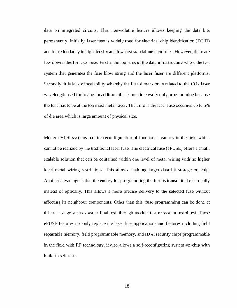
For several decades, laser fuse was the only choice for all the mentioned applications. The
laser fuse employs a top level metal layer, which is intact or blown to store the non-volatile
18
data on integrated circuits. This non-volatile feature allows keeping the data bits
permanently. Initially, laser fuse is widely used for electrical chip identification (ECID)
and for redundancy in high density and low cost standalone memories. However, there are
few downsides for laser fuse. First is the logistics of the data infrastructure where the test
system that generates the fuse blow string and the laser fuser are different platforms.
Secondly, it is lack of scalability whereby the fuse dimension is related to the CO2 laser
wavelength used for fusing. In addition, this is one time wafer only programming because
the fuse has to be at the top most metal layer. The third is the laser fuse occupies up to 5%
of die area which is large amount of physical size.
Modern VLSI systems require reconfiguration of functional features in the field which
cannot be realized by the traditional laser fuse. The electrical fuse (eFUSE) offers a small,
scalable solution that can be contained within one level of metal wiring with no higher
level metal wiring restrictions. This allows enabling larger data bit storage on chip.
Another advantage is that the energy for programming the fuse is transmitted electrically
instead of optically. This allows a more precise delivery to the selected fuse without
affecting its neighbour components. Other than this, fuse programming can be done at
different stage such as wafer final test, through module test or system board test. These
eFUSE features not only replace the laser fuse applications and features including field
repairable memory, field programmable memory, and ID & security chips programmable
in the field with RF technology, it also allows a self-reconfiguring system-on-chip with
build-in self-test.

19
In the history of development of eFUSE using silicided polysilicon, one requirement since
the beginning is that the fuse link requires no additional wafer processing. In addition, the
fuse device needs to be robust across the technology window. In early process
development fuse operation can be adjusted with external voltage stimulus. As the
technology matures, the optimized design of the fuse circuits is converged based on
application needs. Early work on eFUSE focused on thermally rupturing metal fuses but
this material produced significant collateral damage. Later on in subsequent work,
silicided polysilicon showed promising results and the first generation of electrical fuse
was implemented using tungsten silicide polysilicon process. At this stage, eFUSE is used
specifically for DRAM repair. At that time, metal laser fuse was still the preferred method
of manufacture and eFUSE basically mimicked the operation of laser fuse, with high
resistance achieved by breaking the fuse link. There were reliability concerns with this
early non-electro migration fuse work. Because of this reason, metal laser fuse remained
the dominant or preferred choice for this and the next logic technology node.
The second generation of electrical fuse development began with the 0.18um logic
technology using cobalt silicided polysilicon and the basic building block of the fuse
remained the same. The fuse structure was optimized to improve the programming
window. This fuse link introduced programming via electro migration, with no collateral
damage resulting in a wide window of operation. To produce the desired electro migration
phenomena, a programming current of 12mA and anode voltage of 5V range were
established. The fuse achieved typical programmed resistance in excess of 100K ohm with
all fuses over 10K ohm. The fuse link requirements drive the initial circuit designs for the

20
programming FET and sense circuits. This fuse programming and sensing scheme was
migrated to the next technology nodes. There were minimal changes during the migration.
Due to the high programming and sense current requirements, special consideration is
required during design integration of the fuse elements. Legacy designs with excessive
wiring resistance to the fuse circuits exhibited local programming voltage supply pin
(VFSOURCE), drain voltage supply pin(VDD), and ground(GND) variation. This resulted an
inadequate fuse programming condition as well as reduced sense signal margin during
sense operation. It is important to reduce the resistance of VFSOURCE and GND nets. As a
solution for this, distributed or lumped NMOS clamp FETs were added or fitted to the
VFSOURCE lines and a time staggered sensing scheme was devised. This approach allowed
the GND for the sense amplifier to be tightly coupled to the grounded VFSOURCE. By having
this, fuse sensing margin can be improved without degrading the fuse programming
margin.
The electrical fuse solution (IPROG = 10mA and VFSOURCE = 3.5V) was adopted in
manufacturing for select products at the 130nm node. At this time, the design community
was eager to adopt the eFUSE technology across mainstream designs and a single bit kit
was offered for foundry customer solutions. The kit comprised a fuse link, a programming
NMOS FET, and a single ended sense design with a VFSOURCE clamp FET for the 90nm
generation. ASIC library IP block included this kit as part of its library and it is widely
used for embedded dynamic random access memory (eDRAM) redundancy. The eFUSE
kit was employed by the eDRAM system with a self-repair eFUSE controller circuit and

21
built-in-self test (BIST). Since then, eDRAM macros were able to be tested, repaired and
retested in a single touch down on the automated test equipment (ATE).
Variety of specific voltages where used by eDRAM on integrated circuit or chip. These
include the bitline high voltage, the negative wordline low voltage, the wordline boost
voltage and the body bias on the pass transistor. Charge pumps are used to generate all
these voltages on chip which are in turn, set using digital to analog converters (DACs). It
is possible to use the BIST to set these voltages using eFUSE in 90nm eDRAM
technology. This can be done on a die-by-die basis during test to maximize wafer yield.
This is a good example of how on-chip programming coupled with BIST has led to
autonomic capability. Due to the benefits over laser fuse became apparent to the product
design, manufacturing and test communities, the use of eFUSE has spread across different
technology variants. One of the example is that eFUSE solutions were used in IBM’s
90nm bulk and silicon on insulator (SOI) technology products, which includes game
console chips and mainframe chipsets such as the POWER5 microprocessors.
There were additional challenges when scaling into 65nm technology node. Due to
polysilicon process change to nickel silicide, this resulted in a change for the fuse element
post programmed resistance distribution. As a solution to this new challenge, differential
sensing was introduced to offer a robust solution. Several differential sense schemes were
evaluated in order to find the best sensing circuitry.
In the fourth generation of electrical fuse development, low-voltage (IPROG = 7mA and
VFSOURCE = 1.5V) fuse in 65nm and 45nm logic technology were first adopted as starting

22
point. To accommodate a lower fuse programming voltage requirement with standard gate
oxide FETs, the Nikel Silicide fuse element was scaled. The density was also improved
with the One-Time Programmable Read-Only-Memory (OTPROM) architecture. Two
different macros were developed to support a variety of customers’ requirements. First
macro was the general purpose one dimensional linear array offering for bulk foundry
customers who require minimal design migration to the next technology node. Second
macros was the high density two dimensional array OTPROM 4Kb building block IP
offering that can be tiled to create larger arrays.
eFUSE scales with technology but Laser Fuse does not. eFUSE relies on the front end
process technology, but laser fuse relies on the back end process technology. Hence,
eFUSE can be designed to not impact the back end. In short, eFUSE consists of the
following advantages. Firstly, it can be enabled at any level of assembly and function
within the product. Secondly, it does not require any external programming stimulus at
low level (e.g wafer) of processing. eFUSE also exhibits autonomic capability which is
not found in Laser Fuse. As for overall performance, eFUSE is able to make reliable
product “more reliable” (Tonti W., 2008).
2.6 Register Space
The CPU and the PCI devices need to access memory that is shared between them. Device
drivers uses memory to control the PCI devices and to transfer information between them.
Registers normally consist of a small amount of storage. Typically, the shared memory
contains control and status registers for the PCI devices. These registers are used to control

23
the PCI devices and also provides status update to the CPU or host. Some registers have
specific hardware functions such as for power management and performance control.
Others may just store information and may be read-only or write-only. The CPU's system
memory could be used for this shared memory as well. But there is a drawback for this,
where the CPU would have to stall when PCI devices access the memory. CPU can only
resume its task after the PCI device completed its memory access because access to
memory is generally limited to one system component at a time. As a result, the entire
system could be slow down significantly. In addition, it is also not recommended to allow
the system's peripheral devices to access main memory in an uncontrolled way. If there is
a rogue device accesses some core section of the main memory, this could make the
system very unstable and compromised. Accesses by peripheral devices into the system's
memory is very strictly controlled using DMA (Direct Memory Access) channels and
peripheral devices have their own dedicated memory spaces to do its task. ISA (Industrial
Standard Architecture) devices have access to two address spaces, which are ISA I/O
(Input/Output) and ISA memory. On the other hand, PCI devices have access to three
address spaces. They are known as PCI I/O, PCI Memory and PCI Configuration space.
All of these address spaces are accessible by the CPU. For example, device drivers will
be using the PCI I/O and PCI Memory address spaces. PCI initialization code uses PCI
Configuration space within the Linux kernel (Rusling, 1999).
2.6.1 PCI Configuration Space
PCI devices have a set of registers which is known as ‘Configuration Space’. On top of
this register space, The PCI Configuration Space format is shown in Figure 2.5. PCI

24
Express introduces Extended Configuration Space for devices. Configuration space,
including the extended configuration space, registers are mapped to memory locations.
Configuration space registers are accessed by the device drivers and diagnostic software.
Operation systems such as Windows and Linux will have dedicated APIs to allow access
to the device configuration space. However there are cases where operating system does
not have access methods defined or APIs for memory mapped configuration space
requests. Under such condition, the device drivers or diagnostic software has to access
the configuration space in a compatible manner which does not violate the operating
system underlying access rules. In all systems, device drivers are encouraged to use APIs
provided by the operating system for configuration space registers access. PCI Express
defines an Enhanced Configuration Access mechanism (ECAM) for systems that do not
implement a processor architecture specific firmware interface standard that allows
configuration space registers access (Advanced Micro Devices Inc, 2008).