Aging Test Strategy and Adaptive Test Scheduling for SoC Failure
20
Aging Test Strategy and Adaptive Test Scheduling for SoC Failure Prediction Hyunbean Yi, Tomokazu Yoneda, Michiko Inoue, Hiedo Fujiwara, Nara Institute of Science and Technology (NAIST), Japan Yasuo Sato and Seiji Kajihara Kyushu Institute of Technology (KIT), Japan Presenter: Hyunbean Yi
Transcript of Aging Test Strategy and Adaptive Test Scheduling for SoC Failure

Aging Test Strategy and Adaptive Test Scheduling for SoC Failure Prediction
Hyunbean Yi, Tomokazu Yoneda, Michiko Inoue, Hiedo Fujiwara,Nara Institute of Science and Technology (NAIST), Japan
Yasuo Sato and Seiji KajiharaKyushu Institute of Technology (KIT), Japan
Presenter: Hyunbean Yi

2/19
Outline
Motivation and Goal
Background-. Failure Mechanisms
Related Work
Proposed Aging Test Strategy -. Assumptions-. Delay test/measurement scheme-. Adaptive test scheduling
Conclusions

3/19
Motivation and Goal
Highly Reliable Systems -. Satellites, Data/Web servers, Power plants …-. Automobiles, Aircrafts, Medical equipments …
System failure-. Leads to a Catastrophe -. Can occur due to Aging
Failure Prediction-. On-Line self aging test-. Alarm or Self-repair before Failure

4/19
Background – Failure Mechanisms (1/4) Hot Carrier Injection
(HCI)-. In NMOS transistors-. By strong electric field
when Vd > 0.
Negative Bias Temperature Instability (NBTI)-. In PMOS transistors-. Under high temp. environment
when Vg < 0.
Gate
Vg
VdVs
n+ n+
Gate
Vg
VdVs
p+ p+
Gate Insulating Film (SiO2)
HSi
HSi
HSi
HSi
HSi
< Example of HCI >
⇒Threshold Voltage (Vth) ↑ ⇒ Transconductance (gm) ↓ : Performance Degradation !!
< Example of NBTI >

5/19
Background – Failure Mechanisms (2/4)
Time Dependent Dielectric Breakdown (TDDB)-. In Gate Oxide film-. By trapped charges under long time application-. Hopping or Tunneling
Gate
Si< Tunneling due to TDDB >
⇒ Leakage Current ↑⇒ Breakdown !!

6/19
Background – Failure Mechanisms (3/4)
Electromigration (EM) -. By Metal Atom’s migration due to Current Flow
Stress Migration (SM) -. By Metal Atom’s migration due to Thermal Expansion
What is Migration?
< Polycrystalline Structure >
(Source: Sony Semi., “Quality and Reliability Handbook,” 2000)
⇒ Resistance ↑⇒ Disconnection or other defects!!
Before Migration After Migration
: Metal Atom: Defect

7/19
Background – Failure Mechanisms (4/4)
Path
Del
ay
Elapsed Time
NBTI and HCI
Electomigration and Stress Migration
TDDB
< Different Types of Delay Increase >

8/19
Related Work Aging Sensor
-. Delay monitors on actual data paths [Nakura ISSCC’07], [Agarwal VTS’07]
On-Line Self Test Architecture -. CASP (Concurrent Autonomous Chip Self-Test Using Stored Test
Patterns) [Li DATE’08]-. DART (Degrade factor, Accuracy, Report, and Test coverage)
[Sato ASICON’09]
Aging Test Scheduling -. Operating system scheduling [Li, ICCAD’09]
Others …-. Aging path selection [Baba VTS’09], [Noda ETS’10] -. Aging adaptive system [Khan DATE’09]

9/19
Aging Test StrategyPa
th D
elay
Elapsed Time
NBTI and HCI
Electomigration and Stress Migration
TDDB
Degree of aging based test scheduling More aged parts
→ tested more often
Power-on/off time for testing
Various types of delay degradation Detection and Prediction
Accurate delay measure. Consider Volt. and Temp.
< Different Types of Delay Increase > < Delay Variation according to Volt. and Temp. >

10/19
Architecture Overview (1/2)
< SoC Aging Test Architecture >
To improve accuracy -. Multiple Volt. and Temp. sensors-. Thermal-Aware test patterns
SoC
Core
ROMor
NonvolatileMemory
Core Core Core
SoC TestController
Dec
ompr
esso
r
Tclk Gen.
Core Test Controller
k
Protocol Interface
Com
pact
or
k
CPUCore
Core
boot_enable
ExternalMemeory
Test Access Mechanism (TAM)
Functional Interconnect(Bus or Network-on-chip (NoC))
from/toTAM
from/toFunctional
Interconnect
Core Logic
clk
VT Sensors
Core Test
Wrapper
To reduce pattern size-. Aging Path selection -. Compression techniques
11/19
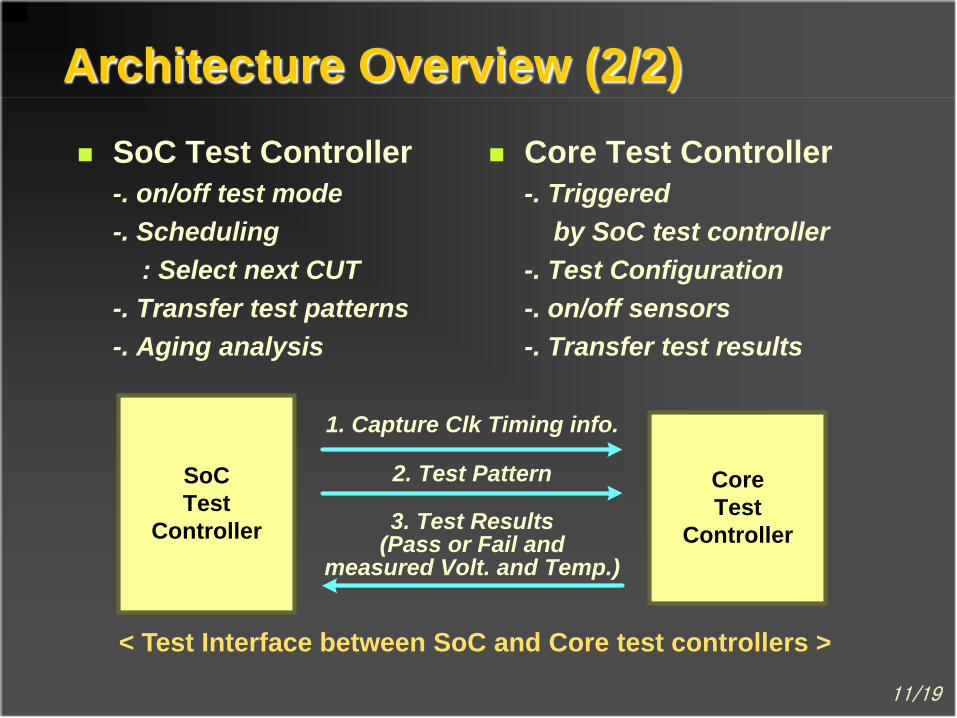
Architecture Overview (2/2) SoC Test Controller
-. on/off test mode-. Scheduling
: Select next CUT-. Transfer test patterns-. Aging analysis
Core Test Controller-. Triggered
by SoC test controller-. Test Configuration-. on/off sensors-. Transfer test results
< Test Interface between SoC and Core test controllers >
1. Capture Clk Timing info.
SoCTest
Controller
CoreTest
Controller
2. Test Pattern
3. Test Results(Pass or Fail and
measured Volt. and Temp.)

12/19
Aging Test FlowStart
Select the TPS to be Applied
Warning?
Delay Test/Measurement for Failure Prediction
More Log Needed?
Aging Detected?
Previous PredictionCanceled?
End
No
No
No
Yes
Yes
Yes Assign a Lower Weight
to the TPSNo
Available for Another
Test Session?
No
Yes
Calculate Remaining Test Time
Assign a High Weight
to the TPS
Yes Alarm
-. DetectSudden delay.
-. Measure amount of Gradual delay.(referring to V. and T.)
-. Calculate amount of aging
-. Log results
-. Compare Degree of Aging (DoA)
-. Assign TPSs to Danger List Tablesconsidering DoA

13/19
Delay Test/Measurement (1/2) Testclock
LCPmin
LCPmax
Functional clock period
Launch Capture
guard-band
< Capture Timing Window >
Path
Del
ay
Elapsed Time
LCPmax
WarningPoint
Failuretest test
LCPmin
Capture timing shift technique-. Adjust Capture Timing
: Launch-to-Capture Period (LCP)-. On-Die Clock Shrink [Josephson ITC’01]
< Using LCP to test a Gradual Delay Increase >

14/19
Delay Test/Measurement (2/2) Test
with LCPmax
Decide the LCPtest
Test with LCPtest
Decrease LCPtest
Increase LCPtest
Calculate Amount of Aging
Report“Warning”
Report“More Log Needed”
Report“Aging
Detected”
Report“Previous Prediction Canceled”
P
P F
F
P F
F P
P: PassF: Fail
< Delay Test/Measurement Flow >
-. Detect Sudden Delay Increase
-. Measure Gradual Delay Increase : Find out
minimum LCPtest
-. Log and Analysis: Volt. & Temp. to Delay
mapping and translation-. Report
Analysis results

15/19
Comparison of Degree of AgingPa
th
Del
ay
Elapsed Time
dworst
BWAW
dA(0)=dB(0)
dC(0)
PUT BPUT A PUT C
CWtest2test1
0n n
gd A t dα∆ = ⋅ ⋅ ⋅
< Examples of Delay Increases of PUTs >
Using Predictive Model of NBTI effect-. ∆dg: Increase in the gate delay
-. ∆dp: Increase in the path delay
-. dA(t): Measured delay of PUT A at time t ( ) (0) nA A Ad t d S t= + ⋅
[Bhardwaj, CICC’06]
npd S t∆ = ⋅
⇒ PUT A and C at test1: dA(test1) = dC(test1),
dA(0) < dC(0),and dA(AW) = dC(CW).
⇒ PUT A and B at test2: dA(test2) > dB(test2),dA(0) = dB(0),and dA(AW) = dB(BW).

16/19
Adaptive Test Scheduling
6
6
Cn TSLCPmax
1 6
9
462
7
59
1
3
42
TPSn
TPSn TPSn TPSn TPSn
Level 1 Level 2 Level 3 … Level n
… … … …
… …
< Danger List Tables >
1→0
0→1
0→1
123
6
45
7
10
89
01
01
0
0
TPSn DF
0
< Scheduling Table >
LessDangerous
MoreDangerous
Tested Less often
TestedMore often
< TPS Information Table >
4
1
5
3
1
22
45
5
1
1
0
1
1
11
10
0
12
16
15
12
10
15
10
16
10
10
Cnter Cnter Cnter Cnter
( : Example of TPS movements)
Priority order of the next TPS to be applied 1. The Remaining TPS in the DLT in the previous test2. The TPS in a higher level DLT of DLTs whose Counter is full.3. In the scheduling table, the next TPSs of which DF is ‘0’.

17/19
Case Study – Environment Settings
Power-on time (= Power-off time) 10 ms
Scan Shift Clock Frequency 75 MHzMaximum Number of Scan Chains
in a Core 32
The Size of Aging Test Patterns Selected for an SoC
1/4 of the total test patterns of an SoC given
Compression Ratio 50xNumber of LCPtest Levels 16
Number of Logged Data for a TPS 10
Maximum size of a TPS: 32 x 25,000 bits (≒ 10 ms / 75 MHz / 10 / 3)
Log size for a TPS: 10 bytes

18/19
Case Study – Size of TP, Tables, and Log ITC’02SoC
Bench.
# of cores
TPsize(bytes)
# of TPSs
S&Isize+ DLTsize(bytes)
Logsize(bytes)
u226 9 23.5 K 29 72.5 145d281 8 2.3 K 12 25.5 60d695 10 0.4 K 10 22.5 50h953 8 0.7 K 8 15 40
g1023 14 0.3 K 14 31.5 70f2126 4 3.1 K 3 4.5 15
q12710 4 11.3 K 7 12.1 35p22810 28 4.1 K 29 76.1 145p34392 19 8.5 K 21 55.1 105p93791 32 15.7 K 29 76.1 145t512505 31 99.6 K 79 246.9 395a586710 7 2.3 M 1184 4.5 K 5.8 K
Average size of test patterns: 206.2 Kbytes Average size of tables: 437.2 bytes Average log amount: 593.7 bytes.

19/19
Conclusions
Aging Test Strategy Failure mechanisms Delay Test/Measurement
-. Considering Volt. and Temp. for Accuracy Degree of aging based Test Scheduling
Future work Aging path selection and PUT grouping Sensor placement Self-repair technique

Thank You !(Taken by A namay , 2009)