Agilent Forward Clocking - Receiver (RX) Jitter Tolerance ... · PDF fileAgilent Forward...
13
Agilent Forward Clocking - Receiver (RX) Jitter Tolerance Test with J-BERT N4903B High-Performance Serial BERT Application Note • All jitter sources built-in (DJ, RJ, ISI, SI) • Half-rate clocking wit duty cycle variation • Common and differential mode interference • Flexible pattern sequencer • Automated measurements for RX and TX physical layer parameters J-BERT N4903B high- performance serial BERT with complete jitter tolerance testing for forward clocking topologies
Transcript of Agilent Forward Clocking - Receiver (RX) Jitter Tolerance ... · PDF fileAgilent Forward...

Agilent
Forward Clocking - Receiver (RX) Jitter
Tolerance Test with J-BERT N4903B
High-Performance Serial BERT
Application Note
• All jitter sources built-in (DJ, RJ, ISI, SI)
• Half-rate clocking wit duty cycle variation
• Common and differential mode interference
• Flexible pattern sequencer
• Automated measurements for RX and TX physical layer parameters
J-BERT N4903B high-performance serial BERT with complete jitter tolerance testing for forward clocking topologies

2
Introduction
This document describes the receiver
(Rx) jitter tolerance test requirements
resulting from forward clocking topolo-
gies. It explains how these requirements
can be efficiently fulfilled for compliance
and characterization test by using the
Agilent J-BERT N4903B high-performance
serial BERT with complete jitter tolerance
testing.
Traditional synchronous clock distribution
reaches a limit at several hundred mega-
bits per second (Mb/s.) As the data rate
goes up, setup and hold times become
increasing critical, particularly given the
manufacturing tolerances of chips and PC
boards. Consequently, designers of chips
and PC boards developed a technique to
skip clock distribution. This technique is
Q uadrup le
C lock arch itectures
C lock
Em bedded
clock
Forwarded clock
(source sychronous)
Full - rate H alf - rate
Q P I
H T 3
(FB -D IM M 2)
(SF I -5)
PC Ie
SATA
U SB
D P
Exam ples: Exam ples:
TX
Link partner Channel DUT
Data
Forwarded
clock
1/2 rate
RX FF
Dll
Figure 1. Clock topology tree
Figure 3. Forward clocking topology
called embedded clocking and uses a data
signal to extract the clock, eliminating the
clock signal routed between the trans-
mitter (Tx) and Rx at the Rx side. This
technique can be used up to ultra high
data rates; however, high-frequency jitter
behavior becomes an issue when clock-
data recovery (CDR) circuits are used.
Additionally, embedded clocking requires
some data coding, adding significant over-
head to the amount of data and raising
the data rate beyond the base rate.
The invention of delay locked loop (DLL)
circuits then helped to push the range of
data rate further, while keeping a clock
distributed. The benefit of this clock topol-
ogy is that the skew can be adjusted to
the setup and hold time requirements at
the receiving end. Consequently, various
types of jitter are added that similar to
clock and data jitter, and the issue of
high-frequency jitter is reduced; Rx func-
tionality and performance is maintained
at data rates in the gigabits per second
(Gb/s) range.
Xilinx popularized the use of forward
clocking topology with help of DLLs in
the Virtex FPGA family [1]. At the time of
writing this document, the main drivers
of forward clocking topology are Intel®
with QuickPath Interconnect (QPI) [2]
and AMD with HyperTransport Gen
3 (HT3) [3]. Other applications using
similar concepts are memory interfaces
like double data rate memory (DDR) and
graphics double data rate memory (GDDR)
[4] and the Serdes Framer Interface Level
5 (SFI-5) [5]. Figure 1 depicts the clocking
topology tree.

3
Forward Clocking Topology
The architecture of the forward clocking
topology is depicted in Figure 2. This
topology is also referred to as half-rate
clocking, since the clock frequency
is typically half of the data rate. It is
also referred to as source synchronous
clocking, since several data lanes are
accompanied by a clock lane running at
half rate. On the Rx side, a DLL circuit
block compensates for tolerances in the
clock distribution network. This provides
several advantages:
• Data and the half-rate clock require
the same bandwidth in the transmitter
output, the channel, and the receiver
input. Any design limitation causes
similar distortion on both the clock and
data.
• In case of jitter due to cross-talk, the
compensation will add-up similar to
data and clock, so at the receiver toler-
ances arrive synchronous and cancel
out.
• The DLL-based clock distribution
eliminates tolerances within the clock
distribution network, thus enabling
the data transfer of multiple lanes at
gigabit speed.
The Difference of Phase-Locked Loop (PLL) versus DLL
The basic concepts of a PLL versus a DLL
are depicted in Figure 3. A PLL is basi-
cally the same as a CDR. So comparing
a PLL and a DLL extracts the differences
between systems based on embedded
clocking versus forward clocking.
The PLL in Figure 3 (right side) uses a volt-
age controlled oscillator, which generates
a clock signal that follows a reference
clock signal. The control logic, consisting
of a phase detector and a loop filter,
adjusts the voltage controlled oscillator’s
(VCO’s) frequency and phase by comparing
the reference input clock with the feedback
clock. When the reference oscillator clock
edge aligns with the feedback clock edge,
the PLL is locked. The loop filter is a low
pass filter of a second or higher order.
The bandwidth of the filter together with
the phase detector is within a couple of
megahertz (MHz.) Consequently, the jitter
tracking depends on the cut-off and peak-
ing/damping characteristics of this filter.
The disadvantage of a CDR is that it cannot
track high-frequency jitter. Thus, jitter
transfer is a weakness of the CDR design
and jitter transfer measurements become
a major task.
The DLL consists of a variable delay line
(VDL) and control logic. The delay line
is implemented as an analog delay line
controlled by a voltage or a digital delay
line containing a chain of gates, or a
mix of both. With the help of the control
logic, the propagation of the delay line is
adjusted until the edges from the clock
input and the feedback clock from the
clock distribution network align. When
the edges line up, the DLL is locked. Thus,
the DLL output clock compensates for the
delay in the clock distribution network.
This compensation is sometimes referred
to as a negative delay generated by the
DLL. In actuality, the DLL incorporates a
handful of clock cycles that can be seen
when running a bursted clock, which is a
valid operating model.
Once locked, there is no need for any
further action, except for some compensa-
tion for very slow drift due to temperature
effects. Fully digital DLLs allow the
control logic to be turned off once the
DLL is locked. The DLL can be designed to
generate clocks with various phases, or it
can incorporate clock doublers, including
a compensation for a clean and exact 50
percent duty cycle. In most systems, a
crystal oscillator generates the system
clock.
Most crystal oscillators produce a signal
with a tolerance of 100 ppm, meaning a
0.01 percent change in the clock period. A
DLL tolerates a frequency drift of signifi-
cantly higher magnitude. The output clock
signal of a DLL reflects any instability
on the input clock signal. This is desired
to track edge changes due to jitter. Any
jitter, including high-frequency jitter, is
tracked by the DLL and is not limited by
the bandwidth of the delay line—which is
as high as the clock rate or higher.
The forward clocking topology uses DLLs
with clock doublers. Clock doublers are
sensitive to the duty cycle distortion of
the input clock. Thus, the variation of the
clock duty cycle is of vital importance for
stress testing. As the propagation path of
the data and clock to the Rx input differs
only for a couple of clock cycles, only very
high frequency jitter may cause an eye
closure due to phase shift. Consequently,
the stress signal for the Rx is mostly com-
posed of inter-symbol interference (ISI)
jitter, with a small amount of standard
random jitter/deterministic jitter (RJ/DJ)
added.
V oltage contro lled de lay line (V D L)
P hase com pare
D LL
C lock dis tribu tion
Figures 3a and 3b. DLL vs. PLL
V oltage contro lled osc illa to r (V C O )
P hase com pare
P LL
R ef clock
C lock dis tribu tion
(3a) (3b)

4
Intel QPI
Starting in 2008, Intel’s new system
architecture and platform technology will
be called Intel QuickPath Technology. It
features new system architecture which
integrates a memory controller into each
microprocessor and connects processors
and other components with a new high-
speed interconnect. Previously announced
under the code name Common System
Interface or CSI, the Intel QuickPath
Technology is designed to allow uninhib-
ited performance of Intel’s future genera-
tions of multi-core processors.
The Intel QPI (also known as QuickPath)
is point-to-point processors intercon-
nected. Each QPI comprises two 20-bit,
point-to-point links. One link is used in
each direction, with a separate clock in
each direction, for a total of 42 signals.
Each signal is a differential pair, so the
total number of pins is 84. Performance
numbers for QPI are reported to be 4.8
to 6.4 Gb/s per data lane. The forwarded
clock runs on a frequency that equals the
data rate divided by two:
Clock frequency = Data rate / 2 (1)
Example: For the data rate of 6.4 Gb/s,
the clock frequency is 3.2 GHz.
The following make the high data rate
possible:
• The differential clock and data
travel together and run at the same
frequency.
• The same crystal drives the reference
clocks on different agents.
• The clock phase and data are “trained”
and aligned at the receiver.
• The receiver sampling is based on the
forwarded clock, while DLLs are used
for clock alignment and multiplying,
thus any jitter is adding to the clock
and data in a similar way and they stay
in phase.
Table 1 lists the parameters for jitter toler-
ance testing of the receiver.
Important aspects for jitter tolerance
margining, also referred to as jitter stress
test, include:
• Forwarded (half rate) clock shall be jit-
ter free, and include variable duty cycle
• The data and clock carry identical
jitter/spread spectrum clocking (SSC)
except for inter-symbol interference
(ISI), which is present on data only
• Data is looped back to bit error ratio
test (BERT) error detector for the bit
error ratio (BER) and jitter tolerance
testing
Symbol ParameterTRX-Gaussian 0.02 UI rms
TRX-DJ 0.3 UI
TRX-SSC 500 ppm @ 33 kHz
TRX-DCD-CLK 0.05 UI
VRX-min-max-ratio 4
VRX-input 200 mV
TRX-input 0.5 UI
VRX-CLK 200 mV
TRX-min pulse 0.6 UI
Table 1. Receiver margining specifi cations

5
The jitter parameters according Table 1
have the following meanings:
1. Rx-Gaussian: Calibrated RJ requested,
amount as specified. This is provided by
J-BERT N4903B as calibrated dial.
2. TRx-DJ: Calibrated ISI is requested. As
the specification is applied at the physical
pin of the receiver package, it may require
to de-embed the actual fixture or to add
some additional ISI. This needs insight
to the design of the actual fixture. A
good practice for the fixture design is to
include a reference trace with coaxial
connectors on both sides. This allows ISI
measurements, as well as collecting the
s-parameters.
If de-embedding is needed, the use of the
Agilent J-BERT N4903B in conjunction
with the Agilent N4916A de-embedding
signal converter is recommended, or if
additional ISI is necessary the use of
the Agilent J-BERT N4903B interference
channel is recommended to add ISI by the
selectable ISI traces.
3. VRx-min-max-ratio: This is another
description of loss by ISI in the channel.
Same recommendation applies as for the
item before (TRx-DJ).
4. TRx-SSC: Calibrated SSC is requested,
amount as specified. This is provided by
the J-BERT N4903B as dial.
5. TRx-DCD-CLK: Calibrated duty-cycle
distortion (DCD) requested, amount as
specified. This is provided by the J-BERT
N4903B as calibrated dial with the divided
clock output.
6. VRx-CLK: This is again a matter of
loss. Using the reference trace is a good
practice. Measure the opening (millivolt
(mV) height at the center of the eye) of
the differential voltage eye of the 1010
Pattern out of the forwarded clock output
as measured over a >100000 unit interval
(UI).
7. TRx-minPulse: A minimum pulse width
has to be applied to the Rx input. This
is due to the ISI caused by the channel.
Using a reference trace as described
under Item 2 is recommended. For calibra-
tion/verification of the required amount
of eye closure, the signal has to be
measured over at least 1000000 UI with
help of a real time scope.
8. VRx-input: This is the voltage eye
(maximum eye height (mV) within a
BER = 1E - 12 contour) that needs to be
obtained by looping back the BERT output
to itself and measuring the eye with a
CDR clock or the forwarded clock looped
back to itself.
The user needs to send a PRBS31 pattern
out of the BERT transmitter, keeping the
external equalizer, if any, off. The jitter
parameters should be tuned within their
maximum specification. Additionally,
the voltage amplitudes, along with any
common mode noise injected, should be
adjusted so as to obey this specification.
9. TRx-input: This is the timing eye
(maximum eye width (UI) within a BER =
1E - 12 contour) that needs to be obtained
by looping back the BERT output to itself
and measuring the eye with a CDR clock
or the forwarded clock looped back to
itself. All the input conditions imposed are
under similar conditions as the VRx-input.
10. VRx-input and TRx-input: These can
be effectively calibrated with the help of
the TRx-input: Agilent J-BERT N4903B
eye contour measurement.
More requirements stated by the standard
and provided by J-BERT N4903B:
• The standalone receiver characteriza-
tion requires a BERT with previously
defined requirements. The BERT should
have a capacity of minimum 12 Gb/s
signaling due to likely future require-
ments, including its CDR and jitter, and
noise injection capabilities.
• Generate an appropriately divided ref-
erence clock from the main forwarded
clock which can be supplied to the
receiver.
• A versatile CDR loop to receive the
looped back transmitter data. The
bandwidth of the CDR must be high
enough to integrate most of the noise
added in the internal loopback path
after the data receiver amplifier.
• Capability to generate user-controlled
delay between the data and the
forwarded clock outputs with fine
granularity (100 fs).

6
HyperTransportTM (HT)
The HyperTransport Consortium is an
industry consortium responsible for
specifying and promoting the computer
bus technology called HyperTransport. HT,
formerly known as lightning data trans-
port (LDT), is a bidirectional serial/parallel
high-bandwidth, low-latency, point-to-
point link that was introduced in 2001.
The technology is used in processors,
in chipsets for PCs, servers, high-perfor-
mance computing devices, and routers.
HT comes in four speed versions—1.x,
2.0, 3.0, and 3.1—which run from 200
MHz to 3.2 GHz (see Table 2.) It is also a
DDR connection, meaning it sends data
on both the rising and falling edges of the
clock signal. This allows for a maximum
data rate of 6400 MT/s when running at
3.2 GHz. The operating frequency is auto-
negotiated. Electrically, HT is similar to
low voltage differential signaling (LVDS)
operating at 2.5 V. HT 2.0 added post-cur-
sor transmitter de-emphasis. HT 3.0 added
scrambling and receiver phase alignment,
as well as optional transmitter pre-cursor
de-emphasis.
The HT signals listed in Table 3 make a
single, unidirectional connection between
two nodes. A full link requires connection
in each direction. HT links wider than
8 bits are built as multiple 8-bit links in
parallel to form either 16- or 32-bit links.
Special features HT 1.x HT 2.0 HT 3.0 HT 3.1Max clock speed 800 MHz 1.4 GHz 2.6 GHz 3.2 GHz
Max aggregate bandwidth
(32-bit links)
12. GB/s 22.4 GB/s 41.6 GB/s 51.2 GB/s
AC operation - capacitive coupling
(optional) with AC/DC auto-
sensing, auto-configuration)
No No Yes Yes
Link splitting (un-ganging); each HT
link split into 2x half-width links
No No Yes Yes
Hot-plugging No No Yes Yes
Dynamic link clock/width adjustment No No Yes Yes
Table 2. HyperTransportTM features summary
HT3 Receiver Specifi cation
The receiver is specified by its measured
input characteristics and its ability to cor-
rectly sample a defined input waveform
with BER 1e-12. The input waveform
definition includes all of the distortions
that a compliant channel can cause to
the waveform generated by the transmit-
ter. This includes amplitude distortions
caused by ISI, crosstalk to both dif-
ferential and common mode propagation,
and the various jitter terms that close the
width of the eye.
Table 4 lists the receiver jitter tolerance
parameters for the HT3 Rx. (Some values
differ for specific operating modes and
when the highest data rates are used.)
The standard defines the reference
plane for compliance testing to be at the
physical pins of the Tx and Rx package.
Consequently, there is a need for a fixture
to hold the chips during test. Probing is
not considered to be a valid alternative.
It would be a wise idea to design the
fixture in a way such that the intercon-
necting traces meet the specifications
of the channel model to achieve the
VRX-DIFF-ratio specified for compliance.
Unfortunately, the operating modes with
and without a decision feedback equalizer
(DFE) and the various data rates, need
some adjust of these values. This adjust-
ment causes a need for additional ISI
and a de-emphasis to reduce ISI for the
various test scenarios.
The J-BERT N4903B with its switchable
ISI traces, together with the N4916A
de-emphasis signal converter, provides
the flexibity to create any necessary
scenario. When the fixture design causes
more ISI than desired, the ISI can be
de-embedded with help of the N4916A.
The J-BERT N4903B contains all types of
jitter sources to create the required stress
for the data signal. The J-BERT N4930B
also provides the half-rate clock with
calibrated variable adjust for delay and
duty cycle.
The J-BERT N4903B comes with cali-
brated jitter sources and the amount of
jitter is simply dialed-in to set. Calibration
is not necessary. While the level param-
eters can be easily chosen, adjustment of
the minimum differential amplitudes must
be made due to the losses of the FR4 Tx-
lines. For this purpose, it is a wise to add
a reference trace into the fixture design
that is the same length and has coaxial
connectors at both ends. This can be
efficiently used for connecting a generator
and scope to make adjustments and char-
acterize the fixture for its S-parameters.

7
Signal Width Description
CAD 2, 4, 8, 16, or 32 Command, addresses, and data (CAD); carries
HyperTransport requests, responses, addresses, and
data; CAD width can be different in each direction
CTL 1, 2, or 4 Differentiates control and data; each byte of CAD has a
CTL signal in Gen3 protocol; one CTL signal is used for
an entire link in Gen1 protocol
CLK 1, 2, or 4 Clocks for the CAD and CTL signals; each byte of CAD
and its respective CTL signal has a separate clock signal
Table 3. HyperTransportTM link signals
Symbol ParameterVRX-DIFF-DC min 170 mV
VRX-DIFF-AC min 120 mV
VRX-DIFF_ratio 4
VRX-CM-AC 350 mV
TRX-EYE 0.4 UI
TRX-DJ-DD 0.5 UI
TRX-CLK-TJ-HF 0.1 UI
TRX-CAD-PW 0.55 UI
TRX-DCLK-PW 0.85 UT
Table 4. Receiver compliance specifufications
The jitter parameters according Table 4
have the following meanings:
VRx-DIFF-DC/AC: Minimum differential
amplitude to be adjusted at the pin. A
de-emphasis may be required to keep
maximum differential amplitude within
specification limits.
VRx-DIFF-ratio: Caused by ISI included
in fixture, the VRX-DIFF-ratio is required
to adjust for various operating modes
according to the actual data rate. The
switchable ISI traces of the J-BERT
N4903B, together with N4916A de-
emphasis signal converter are applicable.
VRx-CM-AC: A common mode voltage
applied from the J-BERT N4903B ISI/SI
converter.
TRx-EYE: Receiver jitter tolerance eye
width is measured at the BER of 1e-12
relative to the clock (CLK.)
TRx-DJ-DD: The maximum deterministic
jitter that the receiver has to tolerate. The
jitter consists of ISI (from FR4 Tx line, J-
BERT ISI trace and de-emphasized signal
converter) and periodic jitter (PJ.) PJ can
be dialed in from the J-BERT N4903B
when ISI is applied.
TRx-CLK-TJ-HF: Applied to the receiver’s
clock during jitter tolerance test; caused
by high frequency crosstalk within the
channel onto the clock. May need a setup
including further equipment.
TRx-PW-CLK: DCD variation on the
clock, applied by DCD dial of the J-BERT
N4903B.

8
Testing the Rx of the Forward Clocking Topology: Generic Considerations
As previously discussed, a minimum
forward clocking topology consist of data
lanes and a dedicated clock lane running
at half the frequency than that of the data
rate applied to the data lanes.
The Rx jitter tolerance test in general
adds SSC, ISI, PJ, RJ, and SI to the data
lanes and DCD to the clock lane. HT3 add
HF jitter (phase-shifted PJ) and SI to the
clock lane.
Test patterns required for Rx jitter testing
are long pseudo random binary sequence
(PRBS) sequences (like 2^23-1 or 2^31-1),
which are a common pattern for the
J-BERT N4903B.
The J-BERT N4903B (Figure 4) comes
with all the required features for Rx
testing:
• Half rate clock with variable duty cycle
on the generator
• Fully calibrated jitter sources RJ, PJ,
SJ, SSC, and residual SSC on data; SSC
and phase shifted PJ on clock
• ISI traces and SI with common/dif-
ferential mode on data
• BER and jitter tolerance measurement,
and more high-level measurements for
Rx and Tx
• Generation of de-embedded signals
with help of the N4916A
Figure 4. J-BERT N4903B together with the N4916A De-Emphasis Signal Converter for
testing a forward clocking topology
9
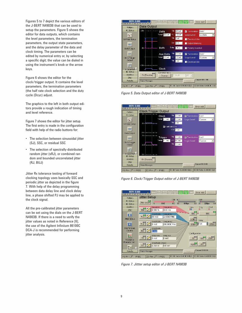
Figures 5 to 7 depict the various editors of
the J-BERT N4903B that can be used to
setup the parameters. Figure 5 shows the
editor for data outputs, which contains
the level parameters, the termination
parameters, the output state parameters,
and the delay parameter of the data and
clock timing. The parameters can be
edited by numerical entry or, by selecting
a specific digit; the value can be dialed in
using the instrument’s knob or the arrow
keys.
Figure 6 shows the editor for the
clock/trigger output. It contains the level
parameters, the termination parameters
(the half rate clock selection and the duty
cycle (Dcyc) adjust.
The graphics to the left in both output edi-
tors provide a rough indication of timing
and level reference.
Figure 7 shows the editor for jitter setup.
The first entry is made in the configuration
field with help of the radio buttons for:
• The selection between sinusoidal jitter
(SJ), SSC, or residual SSC
• The selection of spectrally-distributed
random jitter (sRJ), or combined ran-
dom and bounded uncorrelated jitter
(RJ, BUJ)
Jitter Rx tolerance testing of forward
clocking topology uses basically SSC and
periodic jitter as depicted in the figure
7. With help of the delay programming
between data delay line and clock delay
line, a phase shifted PJ may be applied to
the clock signal.
All the pre-calibrated jitter parameters
can be set using the dials on the J-BERT
N4903B. If there is a need to verify the
jitter values as noted in Reference [6],
the use of the Agilent Infiniium 86100C
DCA-J is recommended for performing
jitter analysis.
Figure 5. Data Output editor of J-BERT N4903B
Figure 6. Clock/Trigger Output editor of J-BERT N4903B
Figure 7. Jittter setup editor of J-BERT N4903B

10
Figure 8. Amplitude Ratio of a PRBS 2^23-1 at 6.4 Gb/s over J-BERT
N4903B ISI trace 2
Figure 9. The amplitude degradation by the ISI trace creates also ISI
jitter in time: 67 ps (equivalent to 430 mUI)
Testing the Rx of a Forward Clocking Topology: Specifi c Considerations
HT3 requires FR4 traces to add ISI jitter.
ISI jitter creates impairment in amplitude
and time. The J-BERT N4903B–020 pro-
vides a set of PC board traces to add such
ISI. With Trace 2 and the required PRBS
2^23-1 pattern, the specified amplitude
ratio of 1:4 can be obtained as shown in
Figure 8. The single bit is down in refer-
ence to several consecutive bits (marker
reading 62 mV / 246 mV = ¼ .)
Such ISI creates a timing jitter of 67 ps
(equivalent to 430 mUI) as shown in
Figure 9. This timing jitter has to be taken
into account when adding further jitter
components for a typical eye closure total
of 0.5. Consequently, there is just room for
70 mUI of sinusoidal jitter to be added as
shown in Figure 7.
Practically, the fixtures holding the DUT
are made from FR4 material so there may
be a significant amount of ISI already built
in, which can create the need to com-
pensate for, rather than add, ISI. In this
case, the use of the N4916A De-emphasis
Signal Converter is recommended. For
details see Reference [7].
With the HT3 standard there are two
more specific requirements:
• The Rx may contain decision feedback
equalization (DFE)
• The Rx jitter tolerance test puts jit-
ter/SI onto the forward clock
The test setup to address these require-
ments is shown in Figure 10. In this
example, the J-BERT N4903B is used
together with the N4916A De-emphasized
Signal Converter and the Agilent 81150A
Pulsar.
The HT3 Rx may use Decision Feedback
Equalization (DFE). The DFE test requires
a large variation of the amplitude ratio
(transitional bit versus de-emphasized
bit.) As shown in Figure 11, combin-
ing the connections of the N4916A
De-emphasized Signal Converter with
the J-BERT N4903B and the ISI traces
in the interference channel module is
recommended. The data generated runs
first through the N4916A de-emphasized
signal converter and then through the
ISI trace. The ISI trace is selected for
the maximum amplitude ratio needed,
and can then be reduced by dialing in
the de-emphasis ratio. The output of the
interference module connects to the data
input of the DUT.
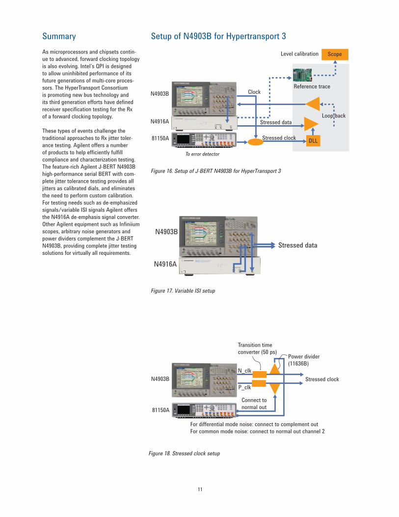
The stressed clock can be achieved with
help of the following methods:
• Adding a differential external source
(such as the 81150A pulse function
arbitrary noise generator) See Figure 12.
• Using the J-BERT N4903B’s embedded
PJ jitter source on the data and clock
with a phase shift (delay between
delay lines), see Figure 7.
The stressed clock setup, as shown in
Figure 12, uses transition time converters
(N4915A-001) to slow down the edge
speed, and power dividers (Agilent
11636B) to combine the data signal and
the modulating signal. When differentially
adding the modulating signal creates DCD
type of jitter, it is important to monitor the
modulated data signal for the minimum
differential eye height. In general, this
kind of external modulation provides more
flexibility, and is the more complex and
expensive solution. (For more details on
jitter modulation, see References [8], [9],
and [10].)
When using the delayed PJ on the clock
as depicted in Figure 7, the amount of
clock jitter results from the phase shift
of the PJ signal between data and clock
signal.
11
Figure 16. Setup of J-BERT N4903B for HyperTransport 3
Figure 17. Variable ISI setup
Figure 18. Stressed clock setup
Setup of N4903B for Hypertransport 3
N4903B
N4916A
Stressed data
Summary
As microprocessors and chipsets contin-
ue to advanced, forward clocking topology
is also evolving. Intel’s QPI is designed
to allow uninhibited performance of its
future generations of multi-core proces-
sors. The HyperTransport Consortium
is promoting new bus technology and
its third generation efforts have defined
receiver specification testing for the Rx
of a forward clocking topology.
These types of events challenge the
traditional approaches to Rx jitter toler-
ance testing. Agilent offers a number
of products to help efficiently fulfill
compliance and characterization testing.
The feature-rich Agilent J-BERT N4903B
high-performance serial BERT with com-
plete jitter tolerance testing provides all
jitters as calibrated dials, and eliminates
the need to perform custom calibration.
For testing needs such as de-emphasized
signals/variable ISI signals Agilent offers
the N4916A de-emphasis signal converter.
Other Agilent equipment such as Infiniium
scopes, arbitrary noise generators and
power dividers complement the J-BERT
N4903B, providing complete jitter testing
solutions for virtually all requirements.
N4903B
Stressed clockDLL
Loop-back
Reference trace
ScopeLevel calibration
To error detector
Stressed data
Clock
N4916A
81150A
N4903B Stressed clock
Connect to
normal out
For differential mode noise: connect to complement out
For common mode noise: connect to normal out channel 2
81150A
P_clk
N_clk
Transition time
converter (50 ps)Power divider
(11636B)

12
Related Products
• J-BERT N4903A High-Performance
Serial BERT with complete jitter toler-
ance testing
• N4916A Industry-first De-Emphasis
Signal Converter
• Infiniium 86100C DCA-J wideband
oscilloscope
• Infiniium DSA91304A High
Performance Oscilloscope: 13GHz
• 81150A Pulse Function Arbitrary Noise
Generator
• 1636B Power Divider, DC to 26.5 GHz
Related Literature
J-BERT N4903B High-Performance Serial
BERT Data Sheet 5990-3217EN
Second Generation PCI EXPRESS
Testing with the J-BETR N4903A High-
Performance Application Note
5989-4087EN
81150A Pulse Function Arbitrary Noise
Generator Data Sheet Version 1.05
Data Sheet 5989-6433EN
Infiniium DCA-J Wide-Bandwidth
Oscilloscope - Mainframe & Module
Technical Specs Data Sheet 5989-0278EN
Agilent Technologies Infiniium DSO/DSA
90000A Series Real-Time Oscilloscope
Data Sheet 5989-7819EN
References
[1] Xilinx clock management applica-
tion notes:
www.xilinx.com/support/documenta-
tion/application_notes/xapp174.pdf
and
www.xilinx.com/support/documenta-
tion/application_notes/xapp132.pdf
[2] Intel QuickPath Technology: www.
intel.com/technology/quickpath/
[3] HyperTransport I/O Link
Specification: http://www.hyper-
transport.org/docs/spec/HTC200393-
0031-0001.pdf
[4] Designing and Validating High-
Speed Memory Buses, Application
Note 1382-2
Literature number 5988-4497EN
[5] Serdes Framer Interface Level 5
(SFI-http://www.oiforum.com/pub-
lic/documents/OIF-SFI5-01.0.pdf
[6] Precision Jitter Analysis Using the
Agilent 86100C DCA-J, application note
Literature number 5989-1146EN
[7] De-emphasized Signal Generation
with the Agilent N4916A
De-Emphasis Signal Converter,
application note
Literature number 5989-7193EN
[8] Calibrated Jitter, Jitter Tolerance Test
and Jitter Laboratory with the Agilent
J-BERT N4903A, application note
Literature number 5989-4967EN
[9] Flexible Signal Conditioning with the
Help of the Agilent 81134A Pulse
Pattern Generator, application note
Literature number 5989-8094EN
[10] Total Jitter Measurement at Low
Probability Levels, Using Optimized
BERT Scan Method, application note
Literature number 5989-2933EN
Glossary
BER Bit error ratio
BERT Bit error ratio tester
BUJ Bounded uncorrelated jitter
CDR Clock-data recovery
CLK Clock
CSI Common system interface
Dcyc Duty cycle
DCD Duty cycle distortion
DFE Decision feedback equalizer
DJ Deterministic jitter
DLL Delay-locked loop
DDR Double data rate
FR4 PC board material
GDDR Graphics double data rate
HT3 HyperTransport Gen 3
HT HyperTransport
ISI Inter-symbol interference
LVDS Low voltage differential signaling
PLL Phase-locked loop
PJ Periodic jitter
PRBS Pseudo random binary sequence
QPI Quick path interconnect
RJ Random jitter
Rx Receiver or receive
SI Signal integrity
SJ Sinusoidal jitter
SSC Spread spectrum clocking
SFI-5 Serdes framer interface Level 5
sRJ Spectrally-distributed random jitter
Tx Transmitter or transmit
UI Unit interval
VCO Voltage controlled oscillator
VDL Variable delay line

Remove all doubt
Our repair and calibration services
will get your equipment back to you,
performing like new, when prom-
ised. You will get full value out of
your Agilent equipment through-
out its lifetime. Your equipment
will be serviced by Agilent-trained
technicians using the latest factory
calibration procedures, automated
repair diagnostics and genuine parts.
You will always have the utmost
confidence in your measurements.
For information regarding self
maintenance of this product, please
contact your Agilent office.
Agilent offers a wide range of ad-
ditional expert test and measure-
ment services for your equipment,
including initial start-up assistance,
onsite education and training, as
well as design, system integration,
and project management.
For more information on repair and
calibration services, go to:
www.agilent.com/find/removealldoubt
Agilent Email Updates
www.agilent.com/find/emailupdates
Get the latest information on the
products and applications you select.
For more information on Agilent Technol-ogies’ products, applications or services, please contact your local Agilent office.
The complete list is available at:
www.agilent.com/find/contactus
AmericasCanada (877) 894-4414 Latin America 305 269 7500United States (800) 829-4444
Asia PacificAustralia 1 800 629 485China 800 810 0189Hong Kong 800 938 693India 1 800 112 929Japan 0120 (421) 345Korea 080 769 0800Malaysia 1 800 888 848Singapore 1 800 375 8100Taiwan 0800 047 866Thailand 1 800 226 008
Europe & Middle EastAustria 01 36027 71571Belgium 32 (0) 2 404 93 40 Denmark 45 70 13 15 15Finland 358 (0) 10 855 2100France 0825 010 700* *0.125 €/minute
Germany 07031 464 6333 Ireland 1890 924 204Israel 972-3-9288-504/544Italy 39 02 92 60 8484Netherlands 31 (0) 20 547 2111Spain 34 (91) 631 3300Sweden 0200-88 22 55Switzerland 0800 80 53 53United Kingdom 44 (0) 118 9276201Other European Countries: www.agilent.com/find/contactusRevised: October 6, 2008
© Agilent Technologies, Inc. 2009Printed in USA, March 24, 20095990-3575EN
Product specifications and descriptions in this document subject to change without notice.
www.agilent.comIntel is a U.S. registered trademark and
Celetron is a U.S. registered trademark of
Intel Corporation.
PCI EXPRESS and the PCI SIG design
marks are registered trademarks and/or
service markes of PCI-SIG.