Agilent E8267C PSG Vector Signal...
24
Agilent E8267C PSG Vector Signal Generators Data Sheet All specifications and characteristics apply over a 0 to 55 °C range (unless otherwise stated) and apply after a 45 minute warm-up time. Supplemental characteristics, denoted as typical or nominal, provide additional (non-warranted) information. Definitions Specifications (spec): represent warranted performance. Typical (typ): performance is not warranted. It applies at 25 °C. A minimum of 80% of all products meet typical performance. Nominal (nom): values are not warranted. They represent the value of a parameter that is most likely to occur; the expected or mean value. They are included to facilitate the application of the product. Standard (std): No options are included when referring to the signal generator unless noted otherwise. PSG Signal Generators Option 520 Option 540 250 kHz to 20 GHz 250 kHz to 40 GHz CW only E8247C E8247C Analog E8257C E8257C Vector E8267C (See E8247C/E8257C data sheet for PSG CW and analog signal generator specifications)
Transcript of Agilent E8267C PSG Vector Signal...
Agilent E8267CPSG Vector Signal Generators
Data Sheet
All specifications and characteristics apply over a 0 to 55 °C range (unless otherwise stated) and apply after a 45 minute warm-up time.Supplemental characteristics, denoted as typical or nominal, provide additional (non-warranted) information.
Definitions
Specifications (spec): represent warranted performance.
Typical (typ): performance is not warranted. It applies at 25 °C. A minimum of 80% of allproducts meet typical performance.
Nominal (nom): values are not warranted. They represent the value of a parameter that is most likelyto occur; the expected or mean value. They are included to facilitate the application of the product.
Standard (std): No options are included when referring to the signal generator unless noted otherwise.
PSG Signal Generators
Option 520 Option 540250 kHz to 20 GHz 250 kHz to 40 GHz
CW only E8247C E8247CAnalog E8257C E8257CVector E8267C
(See E8247C/E8257C data sheet for PSG CW andanalog signal generator specifications)
2
Specifications . . . . . . . . . . . . . . . . . . . . . . . . . . . . . . . . . . . . . . . . . . . . . . . . . . . . . .3Frequency . . . . . . . . . . . . . . . . . . . . . . . . . . . . . . . . . . . . . . . . . . . . . . . . . . . .3Digital sweep . . . . . . . . . . . . . . . . . . . . . . . . . . . . . . . . . . . . . . . . . . . . . . . . .4Ramp (analog) sweep . . . . . . . . . . . . . . . . . . . . . . . . . . . . . . . . . . . . . . . . . .4Output . . . . . . . . . . . . . . . . . . . . . . . . . . . . . . . . . . . . . . . . . . . . . . . . . . . . . . .5Spectral purity . . . . . . . . . . . . . . . . . . . . . . . . . . . . . . . . . . . . . . . . . . . . . . . .7Frequency modulation . . . . . . . . . . . . . . . . . . . . . . . . . . . . . . . . . . . . . . . . .10Phase modulation . . . . . . . . . . . . . . . . . . . . . . . . . . . . . . . . . . . . . . . . . . . .10Amplitude modulation . . . . . . . . . . . . . . . . . . . . . . . . . . . . . . . . . . . . . . . . .10Wideband AM . . . . . . . . . . . . . . . . . . . . . . . . . . . . . . . . . . . . . . . . . . . . . . .11External modulation inputs . . . . . . . . . . . . . . . . . . . . . . . . . . . . . . . . . . . . .11Simultaneous modulation . . . . . . . . . . . . . . . . . . . . . . . . . . . . . . . . . . . . . .11Internal modulation source . . . . . . . . . . . . . . . . . . . . . . . . . . . . . . . . . . . . .11Pulse modulation . . . . . . . . . . . . . . . . . . . . . . . . . . . . . . . . . . . . . . . . . . . . .12Internal pulse generator . . . . . . . . . . . . . . . . . . . . . . . . . . . . . . . . . . . . . . .13Vector modulation . . . . . . . . . . . . . . . . . . . . . . . . . . . . . . . . . . . . . . . . . . . .14I/Q baseband generator: arbitrary waveform mode . . . . . . . . . . . . . . . . .15I/Q baseband generator: real-time mode . . . . . . . . . . . . . . . . . . . . . . . . .17Wideband external I/Q inputs . . . . . . . . . . . . . . . . . . . . . . . . . . . . . . . . . .19Remote programming . . . . . . . . . . . . . . . . . . . . . . . . . . . . . . . . . . . . . . . . .20General specifications . . . . . . . . . . . . . . . . . . . . . . . . . . . . . . . . . . . . . . . . .20
Input/Output Descriptions . . . . . . . . . . . . . . . . . . . . . . . . . . . . . . . . . . . . . . . . . .20Front panel connectors . . . . . . . . . . . . . . . . . . . . . . . . . . . . . . . . . . . . . . . .20Rear panel connectors . . . . . . . . . . . . . . . . . . . . . . . . . . . . . . . . . . . . . . . . .21Auxiliary I/O connector . . . . . . . . . . . . . . . . . . . . . . . . . . . . . . . . . . . . . . . .23
Options, Accessories, and Related Products . . . . . . . . . . . . . . . . . . . . . . . . . . .23
Web Resources . . . . . . . . . . . . . . . . . . . . . . . . . . . . . . . . . . . . . . . . . . . . . . . . . . . .24
Related Agilent Literature . . . . . . . . . . . . . . . . . . . . . . . . . . . . . . . . . . . . . . . . . . .24
Table of Contents

3
Range1
Option 520 250 kHz to 20 GHzResolutionCW 0.001 HzAll Sweep Modes 0.01 Hz 2
Accuracy Aging rate ± temperature effects± line voltage effectsSwitching speed3 < 12 ms (typical) Phase offset Adjustable in nominal 0.1 ° increments.Frequency bands
Band Frequency range N #1 250 kHz to 250 MHz 1/82 > 250 to 500 MHz 1/163 > 500 MHz to 1 GHz 1/84 > 1 to 2 GHz 1/45 > 2 to 3.2 GHz 1/26 > 3.2 to 10 GHz 17 > 10 to 20 GHz 2
Internal timebase reference oscillatorStandard Option UNR
Aging rate < ±1 x 10⁻⁷/year or < ±3 x10⁻⁸/year or< ±4.5 x 10⁻⁹/day < ±2.5 x 10⁻¹⁰/dayafter 45 days after 30 days
Temperature effects (typical) < ±5 x 10⁻⁸ 0 to 55 °C < ±4.5 x 10⁻⁹ 0 to 55 °CLine voltage effects (typical) < ±2 x 10⁻⁹ for < ±2 x 10⁻¹⁰ for
+5% –10% change ±10% changeExternal reference frequency 1, 2, 2.5, 5, 10 MHz 10 MHz onlyLock range ±0.2 ppm ±1.0 ppmReference outputFrequency 10 MHzAmplitude > +4 dBm into 50 Ω load (typical)External reference inputAmplitude > –3 dBmOption UNR 5 dBm ±5 dB4
Input impedance 50 Ω (nominal)
Specifications
Frequency
1. Useable, but unspecified, down to 100 kHz.2. In ramp sweep mode (Option 007), resolution is limited with narrow spans and slow sweep speeds.
Refer to ramp sweep specifications for more information.3. To within 0.1 ppm of final frequency above 250 MHz or within 100 Hz below 250 MHz.4. To optimize phase noise use 5 dBm ± 2 dB.

4
Operating modes Step sweep of frequency or amplitude or both (start to stop)List sweep of frequency or amplitude or both (arbitrary list)
Sweep rangeFrequency sweep Within instrument frequency rangeAmplitude sweep Within attenuator hold rangeDwell time 1 ms to 60 sNumber of points 2 to 65535 (step sweep)
2 to 1601 per table (list sweep)Triggering Auto, external, single, or GPIB
Operating modes Synthesized frequency sweep(start/stop), (center/span), (swept CW)Power (amplitude) sweep (start/stop)Manual sweepRPG control between start and stop frequenciesAlternate sweepAlternates successive sweeps between current and stored states
Sweep span range Settable from minimum2 to full rangeMaximum sweep rate Start Maximum Max span for
frequency sweep rate 100 ms sweep250 kHz to < 0.5 GHz 25 MHz/ms 2.5 GHz0.5 to < 1 GHz 50 MHz/ms 5 GHz1 to < 2 GHz 100 MHz/ms 10 GHz2 to < 3.2 GHz 200 MHz/ms 20 GHz≥ 3.2 GHz 400 MHz/ms 20 GHz
Frequency accuracy ± 0.05% of span ± timebase (at 100 ms sweep time, for sweep spans less than maximum values given above)Accuracy improves proportionally as sweep time increases 3
Sweep time (forward sweep, not including bandswitch and retrace intervals)Resolution 1 msManual mode Settable 10 ms to 99 secondsAuto mode Set to minimum value determined by maximum sweep rate
and 8757D settingTriggering Auto, external, single, or GPIBMarkers 10 independent continuously variable frequency markersDisplay Z-axis intensity or RF amplitude pulseFunctions M1 to center, M1/M2 to start/stop, marker deltaTwo-tone (master/slave)
measurements 4 Two PSGs can synchronously track each other, with independent control of start/stop frequencies
Network analyzer compatibility Fully compatible with Agilent 8757D scalar network analyzer 5
Also useable with Agilent 8757A/C/E scalar network analyzers for making basic swept measurements.6
Ramp (analog) sweep(Option 007)1
Digital sweep
1. During Ramp sweep operation, AM and Pulse Modulation are useable but not specified; FM, Phase Modulation, Wideband AM and I/Q modulation are not useable.
2. Minimum settable sweep span is proportional to carrier frequency and sweep time. Actual sweep span may be slightly different than desired setting for spans less than [0.00004% of carrier frequency or 140 Hz] x [sweep time in seconds]. Actual span will always be displayed correctly.
3. Typical accuracy for sweep times > 100 ms can be calculated from the equation: [(0.005% of span)/(sweep time in seconds)] ± timebase. Accuracy is not specified for sweep times < 100 ms.
4. For Master/Slave operation use Agilent Technologies part #8120-8806 Master/Slave interface cable.5. When measuring low-pass devices in AC mode, dynamic range may be reduced up to 10dB below 3.2 GHz6. GPIB system interface is not supported with 8757A/C/E, only with 8757D. As a result, some features of the
8757A/C/E, such as frequency display, pass-through mode, and alternate sweep, do not function with PSG signal generators.

5
Output Power 1 (dBm)Frequency range 250 kHz to 3.2 GHz 2 –130 to +13250 kHz to 3.2 GHz (with Option 1E6) 2 –130 to +10> 3.2 to 20 GHz3 –130 to +18Step attenuator from 0 to 115 dB in 5 dB steps 4
Measured maximum available power in CW mode
Attenuator hold range (Same as max power sweep range)Minimum From –15 dBm to maximum specified output
power with step attenuator in 0 dB position.Can be offset using step attenuator.
Amplitude switching speed 5
CW or analog modulation < 5 ms (typical)When using power search < 25 ms (typical)Level accuracy 6 (dB)Frequency > +10 dBm +10 to –10 dBm –10 to –70 dBm –70 to –90 dBm –90 to –110 dBm250 kHz to 2 GHz ±0.6 ±0.6 ±0.7 ±0.8 ±1.4> 2 to 20 GHz ±0.8 ±0.8 ±0.9 ±1.0 ±1.7CW Level accuracy with I/Q modulation (With PRBS modulated data)(relative to CW) 7
With ALC On:QAM or QPSK formats 8 ± 0.2 dBConstant-amplitude formats (FSK, GMSK, etc) ± 0.2 dBWith ALC Off: 9 ± 0.2 dB (typical)
1. Maximum power specification is warranted from 15 to 35 ºC, and is typical from 0 to 15 ºC. Maximum power over the 35 to 55 ºC range typically degrades less than 2 dB.
2. With I/Q modulation on, maximum power specification is typical. With external inputs enabled, (I2 + Q2) > 0.2 Vrms.
3. With I/Q modulation on, maximum power specification is typically +15 dBm. With external inputs enabled, (I2 + Q2) > 0.2 Vrms.
4. The step attenuator provides coarse power attenuation to achieve low power levels. Fine power level adjustment is provided by the ALC (Automatic Level Control) within the attenuator hold range.
5. To within 0.1 dB of final amplitude within one attenuator range.6. Specifications apply in CW and list/step sweep modes over the 15 to 35 ºC temperature range, with
attenuator hold off (normal operating mode). Degradation outside this range, for ALC power levels > –5 dBm,is typically < 0.3 dB. In Ramp sweep mode (with Option 007), specifications are typical. For instruments with Type-N connectors (Option 1ED), specifications are degraded typically 0.2 dB above 18 GHz. Level accuracy is not specified below –110 dBm.
7. If external inputs are used, specification applies with input level (I2 + Q2) = 0.3 Vrms and I/Q modulatorattenuation = 10 dB.
8. Measured with symbol rate > 10 kHz and power ≤ 0 dBm.9. Relative to ALC on, after power search is executed. When applying external I/Q signals with ALC off, output
level will vary directly with I/Q input level.
E8267C model
Frequency (MHz)
26
24
22
20
18
16
140 5000 10000 15000 20000
6
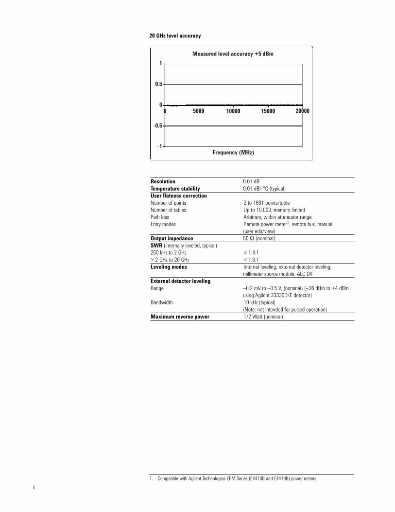
20 GHz level accuracy
Resolution 0.01 dBTemperature stability 0.01 dB/ °C (typical)User flatness correctionNumber of points 2 to 1601 points/tableNumber of tables Up to 10,000, memory limitedPath loss Arbitrary, within attenuator rangeEntry modes Remote power meter1, remote bus, manual
(user edit/view)Output impedance 50 Ω (nominal) SWR (internally leveled, typical)250 kHz to 2 GHz < 1.4:1> 2 GHz to 20 GHz < 1.6:1Leveling modes Internal leveling, external detector leveling,
millimeter source module, ALC OffExternal detector levelingRange –0.2 mV to –0.5 V, (nominal) (–36 dBm to +4 dBm
using Agilent 33330D/E detector)Bandwidth 10 kHz (typical)
(Note: not intended for pulsed operation)Maximum reverse power 1/2 Watt (nominal)
1. Compatible with Agilent Technologies EPM Series (E4418B and E4419B) power meters.
Measured level accuracy +5 dBm
Frequency (MHz)
1
0.5
0
-0.5
-1
0 5000 10000 15000 20000
7
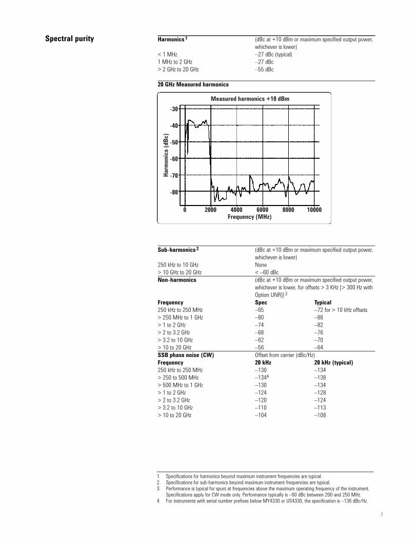
Harmonics 1 (dBc at +10 dBm or maximum specified output power, whichever is lower)
< 1 MHz –27 dBc (typical)1 MHz to 2 GHz –27 dBc> 2 GHz to 20 GHz –55 dBc
20 GHz Measured harmonics
Sub-harmonics 2 (dBc at +10 dBm or maximum specified output power, whichever is lower)
250 kHz to 10 GHz None > 10 GHz to 20 GHz < –60 dBcNon-harmonics (dBc at +10 dBm or maximum specified output power,
whichever is lower, for offsets > 3 KHz [> 300 Hz with Option UNR]) 3
Frequency Spec Typical250 kHz to 250 MHz –65 –72 for > 10 kHz offsets> 250 MHz to 1 GHz –80 –88> 1 to 2 GHz –74 –82> 2 to 3.2 GHz –68 –76> 3.2 to 10 GHz –62 –70> 10 to 20 GHz –56 –64SSB phase noise (CW) Offset from carrier (dBc/Hz)Frequency 20 kHz 20 kHz (typical)250 kHz to 250 MHz –130 –134> 250 to 500 MHz –1344 –138> 500 MHz to 1 GHz –130 –134> 1 to 2 GHz –124 –128> 2 to 3.2 GHz –120 –124> 3.2 to 10 GHz –110 –113> 10 to 20 GHz –104 –108
Spectral purity
1. Specifications for harmonics beyond maximum instrument frequencies are typical.2. Specifications for sub-harmonics beyond maximum instrument frequencies are typical. 3. Performance is typical for spurs at frequencies above the maximum operating frequency of the instrument.
Specifications apply for CW mode only. Performance typically is –60 dBc between 200 and 250 MHz.4. For instruments with serial number prefixes below MY4330 or US4330, the specification is –136 dBc/Hz.
Measured harmonics +10 dBm
Frequency (MHz)
Har
mon
ics
(dB
c)
-30
-40
-50
-60
-70
-80
0 2000 4000 6000 8000 10000

8
Option UNR: Enhanced SSB phase noise (CW) Offset from carrier (dBc/Hz)
Frequency 100 Hz 1 kHz 10 kHz 100 kHzspec (typical) spec (typical) spec (typical) spec (typical)
250 kHz to 250 MHz –94 (–115) –110 (–123) –128 (–132) –130 (–133)> 250 to 500 MHz –100 (–110) –124 (–130) –132 (–136) –136 (–141)> 500 MHz to 1 GHz –94 (–104) –118 (–126) –130 (–135) –130 (–135)> 1 to 2 GHz –88 (–98) –112 (–120) –124 (–129) –124 (–129)> 2 to 3.2 GHz –84 (–94) –108 (–116) –120 (–125) –120 (–125)> 3.2 to 10 GHz –74 (–84) –98 (–106) –110 (–115) –110 (–115)> 10 to 20 GHz –68 (–78) –92 (–100) –104 (–107) –104 (–109)Residual FM CW mode < N x 8 Hz (typical)Option UNR < N x 4 Hz (typical)Ramp sweep mode: < N x 1 kHz (typical) (rms, 50 Hz to 15 kHz bandwidth)Broadband noise(CW mode at +10 dBm or maximum specified output power, whichever is lower, for offsets > 10 MHz)> 2.4 to 20 GHz < –148 dBc/Hz (typical)
Measured phase noise with E5500 and plotted without spurs
1. External I/Q input level (I2 + Q2) = 250 mVrms., I/Q modulator attenuator set to auto.
Standard Phase noise Standard phase noise performance with I/Q modulation on1
Option UNR Option UNR with I/Q modulation on1

9
Measured standard vs. Option UNR at 10 GHz Measured AM noise at 10 GHz
1. Calculated from phase noise performance in CW mode only at +3 dBm. For other frequencies, data rate, or bandwidths, please contact your sales representative.
Typical rms jitter:1
Standard
Carrier SONET/SDH rms jitter Unit intervals Time frequency data rates bandwidth (µUI) (fs)155 MHz 155 MB/s 100 Hz to 1.5 MHz 95 497622 MHz 622 MB/s 1 kHz to 5 MHz 54 552.488 GHz 2488 MB/s 5 kHz to 15 MHz 64 249.953 GHz 9953 MB/s 20 kHz to 80 MHz 162 16
Option UNR
Carrier SONET/SDH rms jitter Unit intervals Timefrequency data rates bandwidth (µUI) (fs)155 MHz 155 MB/s 100 Hz to 1.5 MHz 85 400622 MHz 622 MB/s 1 kHz to 5 MHz 25 392.488 GHz 2488 MB/s 5 kHz to 15 MHz 61 249.953 GHz 9953 MB/s 20 kHz to 80 MHz 158 15

10
Maximum deviation N x 8 MHzResolution 0.1% of deviation or 1 Hz, whichever is greaterDeviation accuracy < ± 3.5% of FM deviation + 20 Hz
(1 kHz rate, deviations < N x 800 kHz)Modulation frequency responsePath Rates (at 100 kHz deviation)
1 dB Bandwidth 3 dB Bandwidth (typical)FM 1 dc/20 Hz to 100 kHz dc/5 Hz to 10 MHzFM 2 dc/20 Hz to 100 kHz dc/5 Hz to 1 MHzdc FM1 carrier offset ±0.1% of set deviation + (N x 8 Hz)Distortion < 1% (1 kHz rate, deviations < N x 800 kHz)Sensitivity ±1 Vpeak for indicated deviationPaths FM1 and FM2 are summed internally for composite
modulation. Either path may be switched to any one ofthe modulation sources: Ext1, Ext2, internal1, internal2.The FM2 path is limited to a maximum rate of 1 MHz. The FM2 path must be set to a deviation less than FM1.
Maximum deviation N x 80 radians(N x 8 radians in high-bandwidth mode)
Resolution 0.1% of set deviationDeviation accuracy < ±5% of deviation + 0.01 radians
(1 kHz rate, normal BW mode)Modulation frequency responseMode Maximum Deviation Rates (3 dB BW)Normal BW N x 80 rad dc – 100 kHzHigh BW N x 8 rad dc – 1 MHz (typical)Distortion < 1 % (1 kHz rate, THD, dev < N x 80 rad,
normal BW mode)Sensitivity ±1 Vpeak for indicated deviationPaths ΦM1 and ΦM2 are summed internally for composite
modulation. Either path may be switched to any one ofthe modulation sources: Ext1, Ext2, internal1, internal2.The ΦM2 path must be set to a deviation less than ΦM1.
Depth Linear mode Exponential (log) mode(Downward modulation only)
Maximum > 90% > 20 dBSettable3 0 to 100 % 0 to 40 dBResolution 0.1% 0.01 dBAccuracy (1 kHz rate) < ±(6 % of setting + 1 %) < ±(2% of setting + 0.2 dB)Ext sensitivity ±1 Vpeak for –1 V for indicated depth
indicated depthRates (3 dB bandwidth, 30% depth) dc/10 Hz to 100 kHz (typical) (useable to 1 MHz)Distortion (1 kHz rate, linear mode, THD)30% AM < 1.5%90% AM < 4 % Paths AM1 and AM2 are summed internally for composite
modulation. Either path may be switched to any one ofthe modulation sources: Ext1, Ext2, internal1, internal2.
Frequency modulation
Phase modulation
Amplitude modulation (fc > 2 MHz)2 (typical)
1. At the calibrated deviation and carrier frequency, within 5 °C of ambient temperature at time of user calibration.2. For fc < 2 MHz AM is usable but not specified. AM specifications apply with ALC on, and envelope peaks
< maximum specified power.3. For AM depth settings > 90% or > 20 dB, deep AM mode is recommended.

11
Rate (typical 1 dB bandwidth)ALC on 1 kHz to 80 MHzALC off DC to 80 MHzExternal 1 input Sensitivity 0.5 V = 100%Input impedance 50 Ω (nominal)
Modulation types AM, FM, and ΦMInput impedance 50 or 600 Ω (nominal), switchedHigh/low indicator(100 Hz to 10 MHz BW, ac coupled inputs only) Activated when input level error exceeds 3% (nominal)
All modulation types may be simultaneously enabled except: FM with ΦM, linear AM withexponential AM, and Wideband AM with I/Q. AM, FM, and ΦM can sum simultaneous inputs from any two sources (Ext1, Ext2, internal1, or internal2) Any given source (Ext1, Ext2, internal1, or internal2) may be routed to only one activated modulation type.
Dual function generators provides two independent signals (internal1 and internal2) for use withAM, FM, ΦM, or LF Out.Waveforms Sine, square, positive ramp, negative ramp, triangle,
Gaussian noise, uniform noise, swept sine, dual sine 1
Rate rangeSine 0.5 Hz to 1 MHzSquare, ramp, triangle 0.5 Hz to 100 kHzResolution 0.5 HzAccuracy Same as timebaseLF outOutput Internal1 or internal2. Also provides monitoring of
internal1 or internal2 when used for AM, FM, or ΦM.Amplitude 0 to 3 Vpeak, into 50 Ω (nominal) Output impedance 50 Ω (nominal) Swept sine mode:(frequency, phase continuous)Operating modes Triggered or continuous sweepsFrequency range 1 Hz to 1 MHzSweep rate 0.5 Hz to 100 kHz sweeps/s, equivalent to
sweep times 10 us to 2 sResolution 0.5 Hz (0.5 sweep/s)
Wideband AM
External modulation inputs(Ext1 & Ext2)
Simultaneous modulation
Internal modulation source
1. Internal2 is not available when using swept sine or dual sine modes.

12
Standard Standard Option 1E6 2
> 3.2 GHz 500 MHz to 3.2 GHz 10 MHz to 3.2 GHzOn/off ratio 80 dB 80 dB (typical) 80 dBRise/fall times (Tr, Tf ) 10 ns (6 ns typical) 100 ns (typical) 10 ns (8 ns typical)Pulse widthInternally leveled ≥ 1µs ≥ 2 µs (typical) ≥ 1µsLevel hold (ALC Off ≥ 20 ns (typical) ≥ 0.5 µs (typical) ≥ 20 ns (typical)
with power search) 3
Repetition frequencyInternally leveled 10 Hz to 500 kHz 10 Hz to 250 kHz 10 Hz to 500 kHz
(typical) (typical) (typical) Level hold (ALC Off with dc to 10 MHz dc to 1 MHz (typical) dc to 10 MHz (typical)
power search) 3 (typical)Level accuracy (relative to CW)Internally leveled ±0.5 dB ± 0.5 dB ± 0.5 dB
±0.15 (typical)Level hold (ALC Off with ≤ 20 GHz ±0.8 dB ±0.5 dB (typical) ± 1.2 dB (typical)
power search) 3 (typical)Width compression ±5 ns (typical) ±50 ns (typical) ±5 ns (typical)Video feed-through 4 < 2 mV (typical) < 200 mV (typical) < 125 mV (typical)Video delay(Ext input to Video) 40 ns (nominal) 40 ns (nominal) 40 ns (nominal) RF delay (Tm)(Video to RF output) 35 ns (nominal) 280 ns (nominal) 45 ns (nominal) Pulse overshoot (Vor) < 10% (typical) < 10% (typical) < 10% (typical)Input level +1 Vpeak = RF On +1 Vpeak = RF On +1 Vpeak = RF OnInput impedance 50 Ω, (nominal) 50 Ω, (nominal) 50 Ω, (nominal)
Pulse modulation1
1. With ALC off, specs apply after the execution of power search. Specs apply with Atten Hold off (default mode), or ALC level between 0 and +10 dBm.
2. Option 1E6 provides narrow pulse (20 ns typical) capability between 10 MHz and 3.2 GHz. Narrow pulse capability above 3.2 GHz is standard.
3. Power search is a calibration routine that improves level accuracy in ALC-off mode. Un-pulsed RF powerwill be present typically up to 50 ms when executing power search.
4. With attenuator in 0 dB position. Video feed-through decreases with attenuator setting.
Measured pulse modulation envelopeFreq = 10GHz, Amp = 10dBM, ALC = OFF, Pulse width = 50ns
Timebase (nsec)
0 10 20 30 40 50 60 70 80 90 100

13
Internal pulse generator Modes Free-run, triggered, triggered with delay, doublet, and gated. Triggered with delay, doublet, and gatedrequire external trigger source.
Period (PRI) (Tp ) 70 ns to 42 s (Repetition frequency: 0.024 Hz to 14.28 MHz)
Pulse width (Tw ) 10 ns to 42 sDelay (Td )Free-run mode 0 to ±42 sTriggered with delay and doublet modes 75 ns to 42 s with ±10 ns jitterResolution 10 ns (width, delay, and PRI)
Syncoutput
Videooutput
RF pulseoutput
Td
Tm
Tw
Trf
Vf
TfTr
Vor
Tp
50%
50%
10%
90%
50%
Td video delay (variable)
Tw video pulse width (variable)
Tp pulse period (variable)
Tm RF delay
Trf RF pulse width
Tf RF pulse fall time
Tr RF pulse rise time
Vor pulse overshoot
Vf video feedthrough

14
External I/Q inputsInput impedance switched 50 or 600 Ω (nominal) Input range 1 Minimum 0.1 Vrms, maximum 1VpeakFlatness ± 1 dB within ± 40 MHz of carrier (with ALC off) (typical)Measured I/Q frequency response 2
I/Q adjustmentsI & Q offsets External inputs (600 Ω) ± 5 Volts
External inputs (50 Ω) ± 50 %Internal baseband generator ± 50 %
I/Q attenuation 0 to 40 dBI/Q gain balance ± 4 dBI/Q quadrature skew ± 10° range (typical)Low pass filter Selectable 40 MHz or throughI/Q baseband outputsDifferential I, I bar, Q, Q barSingle ended I, QFrequency range DC to 40 MHz Output voltage into 50 W 1.5 Vp-p (typical)DC offset adjustments ± 3 VDC offset resolution 1 mVLow pass filter Selectable 40 MHz or though
Vector modulation
Offset from carrier (GHz)
Con
vers
ion
loss
(dB
)
5
0
-5
-10
-15
-0.15 -0.10 -0.05 0.00 0.05 0.10 0.15
Offset from carrier (GHz)
Con
vers
ion
loss
(dB
)
5
0
-5
-10
-15
-0.15 -0.10 -0.05 0.00 0.05 0.10 0.15
Offset from carrier (GHz)
Con
vers
ion
loss
(dB
)
5
0
-5
-10
-15
-0.15 -0.10 -0.05 0.00 0.05 0.10 0.15Offset from carrier (GHz)
Con
vers
ion
loss
(dB
)
5
0
-5
-10
-15
-0.15 -0.10 -0.05 0.00 0.05 0.10 0.15
1.5 GHz 3 GHz
12 GHz 20 GHz
1. For optimum signal quality, the I and Q inputs should be 0.7 V peak, with (I2 + Q2) + 150 mVrms. DifferentRMS levels are accommodated by adjusting the internal I/Q modulator attenuator, which may be either manually or automatically set. The minimum input level required to maintain RF level accuracy is
(I2 + Q2) = 0.1 Vrms. 2. Sine wave response, measured with input level = 100 mVrms on one channel, and ALC off.

15
Channels 2 [I and Q]Resolution 16 bits [1/65,536]Baseband waveform memoryLength (playback) 64 megasamples (MSa)Length (storage) 1.2 gigasamples (GSa) on 6 GB hard drive (Option 005)Waveform segmentsSegment length 60 samples to 64 MSaMaximum number of segments 8192 Minimum memory allocation 256 samples or 1 kbyte blocksWaveform sequencesSequencing Continuously repeatingMaximum number of sequences 16,384Maximum segments/sequence 1 to 32,768Maximum segment repetitions 1 to 65,536ClockSample rate 1 Hz to 100 MHzResolution 0.001 HzAccuracy Same as timebase +2-42 [in non-integer applications]Reconstruction filter: [fixed] 50 MHz [used for all symbol rates]Baseband spectral purity[full scale sinewave]Harmonic distortion 100 kHz to 2 MHz: < –65 dBc (typical)Phase noise < –127 dBc/Hz (typical)
(baseband output of 10 MHz sinewave at 20 kHz offset)IM performance < –74 dB (typical)
(two sinewaves at 950 kHz and 1050 kHz at baseband)TriggersTypes Continuous, single, gated, segment advanceSource Trigger key, external, remote [LAN, GPIB, RS-232]External polarity Negative, positiveExternal delay time 10 ns to 40 sec plus latencyExternal delay resolution 10 nsMarkers(Markers are defined in a segment during the waveform generation process, or from thePSG front panel. A marker can also be tied to the RF blanking feature of the PSG.)
Marker polarity Negative, positiveNumber of markers 4MulticarrierNumber of carriers Up to 100 (limited by a max bandwidth of 80 MHz
depending on symbol rate and modulation type)Frequency offset (per carrier) –40 MHz to +40 MHzPower offset (per carrier) 0 dB to –40 dBModulationPSK BPSK, QPSK, OQPSK, π/4DQPSK, 8PSK,16PSK, D8PSKQAM 4, 16, 32, 64, 256FSK Selectable: 2, 4, 8, 16MSKData Random ONLY
I/Q baseband generator: arbitrary waveform mode(Option 602)

16
Measured multicarrier4 Carriers with 64 QAM at 10 Msym\s with 20 MHz spacing
MultitoneNumber of tones 2 to 64, with selectable on/off state per toneFrequency spacing 100 Hz to 80 MHzPhase (per tone) Fixed or randomPower offset (per tone) 0 to –40 dB
Ref-4 dBmSampLog10dB/
LgAv10W1 S2S3 FC
(f):#f>50K#Swp
#Atten 6 dB
Center 20.000 00 GHzRes BW 1.8 MHz VBW 1.8 MHz
Span 200 MHzSweep 1 ms
Ref 0 dBmNormLog10dB/
LgAv W1 S2S3 FC
(f):#f>50K#Swp
Atten 10 dBMkr1 -38.67 MHz
-41.19 dB
Center 20.000 00 GHz#Res BW 3 kHz VBW 3 kHz
Span 80 MHzSweep 10.72 s
Marker-38.670000 MHz-41.19 dB
Ref-4 dBmSampLog10dB/
LgAv10W1 S2S3 FC
(f):#f>50K#Swp
#Atten 6 dBMkr1 -8.00 MHz
-59.104 dB
Center 20.000 00 GHzRes BW 180 kHz VBW 180 kHz
Span 20 MHzSweep 2.36 ms
Marker-8.000000 MHz-59.104 dB
Measured multitone Measured image rejection > 3.2 GHz

17
Two-toneFrequency spacing 100 Hz to 80 MHz (symmetrical about carrier)IM distortion250 kHz to 3.2 GHz < –45 dBc for RF levels < 0 dBm (typical)>3.2 GHz to 20 GHz < –55 dBc for RF levels < 0 dBm (typical)
Measured two-tone
Basic modulation types (custom format)PSK BPSK, QPSK, OQPSK, π/4DQPSK, 8PSK, 16PSK, D8PSKMSK User-defined phase offset from 0 to 100°QAM 4, 16, 32, 64, 256FSK Selectable: 2, 4, 8, 16 level symmetricUser defined Custom map of up to 16 deviation levelsSymbol rate Maximum deviation< 5 MHz 4 times symbol rate5 MHz to 50 MHz 20 MHzResolution: 0.1 HzI/Q Custom map of 256 unique valuesVector accuracy 1 Formats: BPSK, QPSK, 16-256QAM
(α= 0.3, Root Nyquist filter, symbol rate 4 Msym/s)EVM < 1.2% RMS, < 0.8% RMS (typical)Origin offset250 kHz to 3.2 GHz –45 dBc (typical)3.2 to 20 GHz –50 dBc (typical)FIR filterSelectable Nyquist, root Nyquist, Gaussian, rectangular
α: 0 to 1, BbT: 0.1 to 1Custom FIR 16-bit resolution, up to 64 symbols long, automatically
resampled to 1024 coefficients (max)> 32 to 64 symbol filter: symbol rate ≤ 12.5 MHz> 16 to 32 symbol filter: symbol rate ≤ 25 MHzInternal filters switch to 16 tap when symbol rate isbetween 25 and 50 MHz
Symbol rateFor external serial data: Adjustable from 1000 symbols/sec to a maximum symbol
rate of 50 Mbits/sec ÷ #bits/symbolFor internally generated data: Adjustable from 1000 symbols/sec to 50 Msymbols/sec.
and a maximum of 8 bits per symbol. Modulation quality may be degraded at high symbol rates.
Baseband reference frequency Data clock can be phase locked to an external reference.Input ECL, CMOS, TTL compatible, 50 Ω AC coupled
Internal baseband generator: real-time mode(Option 602)
Ref-4 dBmSampLog10dB/
LgAv10W1 S2S3 FC
(f):#f>50K#Swp
#Atten 6 dBMkr1 -20.00 MHz
-62.275 dB
Center 20.000 00 GHzRes BW 470 kHz VBW 470 kHz
Span 50 MHzSweep 1 ms
Marker-20.000000 MHz-62.275 dB
1. Measured with Agilent 89441A Vector Signal Analyzer. Valid after executing I/Q calibration, and instrument is
maintained within ± 5 °C of calibration temperature. RF power < 0 dBm. When external inputs are used, vector
accuracy can approach internal performance after system optinization. Recommended external I/Q input level
(I2 + Q2) = 0.3 Vrms, I/Q modulator attenuator = 10 dB.

18
Measured EVM
Measured spectral re-growth 5 GHz carrier with 16 QAM signal at 10 Msym/s
Frame trigger delay controlRange 0 to 1,048,575 bitsResolution 1 bitData typesInternally generated dataPseudo-random patterns PN9, PN11, PN15, PN20, PN23Repeating sequence Any 4-bit sequence
Other fixed patternsDirect-pattern RAM [PRAM]Max size 32 Mb
(each bit uses an entire sample space)Use Non-standard framingUser fileMax size 3.2 MBUse Continuous modulation or internally generated
TDMA standardExternally generated dataType Serial dataInputs Data, data (bit) clock, symbol sync
Accepts data rates ±5% of specified data rateInternal burst shape controlVaries with standards and bit ratesRise/fall time range Up to 30 bitsRise/fall delay range 0 to 63.5 bits
QPSK
Symbol rate (Msymbol/sec)
7
6
5
4
3
2
1
00 5 10 15 20 25 30 35 40 45 50
1 GHz3 GHz2 GHz6 GHz20 GHz12 GHz
16QAM
Symbol rate (Msymbol/sec)
5
4.5
4
3.5
3
2.5
2
1.5
1
0.5
00 5 10 15 20 25 30 35 40 45 50
1 GHz3 GHz2 GHz6 GHz20 GHz12 GHz
Ref-8 dBmSampLog10dB/
LgAv100W1 S2S3 FC
(f):#f>50K#Swp
#Atten 8 dBMkr1 12.00 MHz
--64.057 dB
Center 5.000 00 GHzRes BW 470 kHz VBW 470 kHz
Span 50 MHzSweep 1 ms
-64.057 dB

19
RF output frequency range: 3.2 to 20 GHzInputInput (baseband) frequency range DC to > 500 MHz (nominal) Input impedance 50 Ω (nominal) Recommended input level 0 dBm (nominal) Maximum input voltage ±1 volt DC
I/Q offset adjustments ±50%RF path filters 1
Carrier Frequency Low-pass 3 dB cutoff frequency (nominal)> 3.2 to 5 GHz 5.5 GHz> 5 to 8 GHz 8.9 GHz> 8 to 12.8 GHz 13.9 GHz> 12.8 GHz 22.5 GHzMeasured I/Q frequency response
Wideband external I/Q inputs(Option 015)
1. Operation close to RF filter cutoff frequencies will affect channel flatness.
Offset from carrier (GHz)
Con
vers
ion
loss
(dB
)
5
0
-5
-10
-15
-0.4 -0.2 0.0 0.2 0.4
Offset from carrier (GHz)
Con
vers
ion
loss
(dB
)
5
0
-5
-10
-15
-0.4 -0.2 0.0 0.2 0.4
Offset from carrier (GHz)
Con
vers
ion
loss
(dB
)
5
0
-5
-10
-15
-0.4 -0.2 0.0 0.2 0.4
Offset from carrier (GHz)
Con
vers
ion
loss
(dB
)
5
0
-5
-10
-15
-0.4 -0.2 0.0 0.2 0.4
6 GHz 10 GHz
15 GHz 20 GHz
20
Interfaces GPIB (IEEE-488.2,1987) with listen and talk, RS-232,and 10BaseT LAN interface.
Control languages SCPI version 1997.0. Also will emulate most applicable Agilent 836xxB, Agilent 837xxB, and Agilent 8340/41B commands, providing general compatibility with ATEsystems which include these signal generators.
IEEE-488 functions SH1, AH1, T6, TE0, L4, LE0, SR1, RL1, PP0, DC1, DT0, C0, E2.ISO compliant This family of signal generators is manufactured in an
ISO-9001 registered facility in concurrence withAgilent Technologies commitment to quality.
Power requirements 90 to 267 VAC 50 to 60 Hz, (automatically selected),650 W maximum.
Operating temperature range 0 to 55 °C1
Storage temperature range2 –40 to 71 °CWith Option 005: –4 ° to 65 °C, gradient less than 20 °C/hour
Shock and vibrationOperating random vibration 5 to 500 Hz, 0.21 g rmsSurvival swept sine vibration 5 to 500 Hz, 0.75 g Survival random vibration 5 to 500 Hz, 2.09 g rms Functional shock (half-sine, 30 g, 11 ms) Meets the requirements of MIL-PRF-28800F for classand bench drop test 3 equipment.EMC Meets the conducted and radiated interference and
immunity requirements of IEC/EN 61326-1. Meets radiated emission requirements of CISPR Pub 11/1997Group 1 class A.
Storage registers Memory is shared by instrument states, user data files, sweep list files, and waveform sequences. Depending on the number and size of these files, up to 800 storage registers and 10 register sequences are available.
Security Display blanking.Compatibility Agilent Technologies 83550 Series millimeter heads (not
for use with I/Q modulation), Agilent Technologies 8757Dscalar network analyzers, Agilent Technologies EPM Series power Meters.
Self-test Internal diagnostic routine tests most modules (including microcircuits) in a preset condition. For each module, if itsnode voltages are within acceptable limits, then the module “passes” the test.
Weight < 25 kg (54 lb.) net, < 33 kg (74 lb.) shipping.Dimensions 178 mm H x 426 mm W x 498 mm D
(7” H x 16.8” W x 19.6” D in.).Recommended calibration cycle 24 months
RF output Nominal output impedance 50 Ω. Precision APC-3.5 male, or Type-N with Option 1ED.
ALC input Used for negative external detector leveling.Nominal input impedance 120 kΩ, damage level ±15 V.
LF output Outputs the internally generated LF source. Nominal output impedance 50 Ω.
External input 1 Drives either AM, FM, or ΦM. Nominal input impedance 50 or 600 Ω, damage levels are 5 Vrms and 10 Vpeak.
Remote programming
General specifications
Front panel connectors(All connectors are BNC femaleunless otherwise noted.) 3
1. Save and recall of user files and instrument states from Option 005 Hard Drive is guaranteed only over the range 0 to 40 °C.
2. Storage below –20 °C instrument states may be lost.3. Digital inputs and output are 3.3 V CMOS unless indicated otherwise. Inputs will accept 5 V CMOS, 3V CMOS,
or TTL voltage levels.
Input/OutputDescriptions
21
External input 2 Drives either AM, FM, or ΦM. Nominal input impedance 50 or 600 Ω, damage levels are 5 Vrms and 10 Vpeak.
Pulse/trigger gate input Accepts input signal for external fast pulse modulation. Also accepts external trigger pulse input for internal pulsemodulation. Nominal impedance 50 Ω. Damage levels are 5 Vrms and 10 Vpeak.
Pulse video out Outputs a signal that follows the RF output in all pulse modes. TTL-level compatible, nominal source impedance 50 Ω.
Pulse sync out Outputs a synchronizing pulse, nominally 50 ns width,during internal and triggered pulse modulation. TTL-level compatible, nominal source impedance 50 Ω.
Data clock input Accepts a data clock signal to synchronize serial data for usewith internal baseband generator (Option 602). Maximumrate 50 MHz. Damage levels are > + 5.5 and < –0.5 V.
Data input Accepts serial data for use with internal baseband generator(Option 602). Maximum rate 50 Mb/s. Data must be validon the falling edges of data clock (normal mode) or the symbol sync (symbol mode). Damage levels are > + 5.5 and < –0.5 V.
I input Accepts an "I" input either for I/Q modulation or for wideband AM. Nominal input impedance 50 or 600 Ω. Damage levels are 1 Vrms and 5 Vpeak.
Q input Accepts a "Q" input for 1/0 modulation. Nominal input impedance 50 or 600 Ω. Damage levels are 1 Vrms and 5 Vpeak.
Symbol sync input Accepts symbol sync signal for use with internal basebandgenerator (Option 602). Symbol sync might occur once per symbol or be a single, one bit wide pulse to synchronizethe first bit of the first symbol. Maximum rate 50 MHz. Damage levels are > +5.5 and < –0.5 V.
Auxillary interface (Dual mode) Used for RS-232 serial communication and for Master/Slavesource synchronization. (9-pin D-subminiature female connector) For Master/Slave operation use Agilent Technologies part #8120-8806 Master/Slave interface cable.
GPIB Allows communication with compatible devices.LAN Allows 10baseT LAN communication10 MHz input Accepts an external reference (timebase) input (at 1, 2,
2.5, 5, 10 MHz for standard and 10 MHz only for Option UNR) Nominal input impedance 50 Ω. Damage levels > +10 dBm
10 MHz output Outputs internal or external reference signal. Nominal output impedance 50 Ω. Nominal output power +4 dBm
Sweep output (Dual mode) Supplies a voltage proportional to the RF power or frequency sweep ranging form 0 volts at the start of sweep to +10 volts (nominal) at the end of sweep, regardless of sweep width.
When connected to an Agilent 8757D scalar network analyzer (Option 007), generates a selectable number of equally spaced 1 us pulses (nominal) across a ramp (analog) sweep. Number of pulses can be set form 101 to 1601 by remote control from the 8757D.
Output impedance: < 1 Ω, can drive 2000 Ω.
Rear panel connectors(All connectors are BNC femaleunless otherwise noted.) 1
1. Digital inputs and output are 3.3 V CMOS unless indicated otherwise. Inputs will accept 5 V CMOS, 3V CMOS,or TTL voltage levels.

22
Stop sweep In/Out Open-collector, TTL-compatible input/output. In ramp sweep operation, provides low level (nominally 0 V) duringsweep retrace and bandcross intervals, and high level during the forward portion of the sweep. Sweep will stopwhen grounded externally, sweep will resume when allowed to go high.
Trigger output (Dual mode) Outputs a TTL signal. High at start of dwell, or when waitingfor point trigger; low when dwell is over or point trigger isreceived, In ramp sweep mode, provides 1601 equally-spaced1us pulses (nominal) across a ramp sweep. When using LF out, provides 2 us pulse at start of LF sweep.
Trigger input Accepts TTL signal for triggering point-to-point in manual sweep mode, or to trigger start of LF sweep. Damage levels ≥ +10 V or ≤ –4 V.
Source module interface Provides bias, flatness correction, and levelingconnections to the Agilent model 83550 Series mm-wavesource modules.
Source settled Provides an output trigger that indicates when the signal generator has settled to a new frequency or power level.High indicates source not settled, Low indicates source settled.
Z-axis Blank/Markers During ramp sweep, supplies +5 V (nominal) level duringretrace and bandswitch intervals. Supplies –5 V (nominal) level when the RF frequency is at a marker frequency.
10 MHz EFC (Option UNR only) Accepts an external DC voltage, rangingfrom –5 V to +5 V, for electronic frequency control (EFC)of the internal 10 MHz reference oscillator. This voltage inversely tunes the oscillator about its center frequency approximately –0.07 ppm/V. The nominal input impedanceis greater than 1 M.
.25 – 3.2 GHz coherent carrier output Outputs RF signal modulated with FM or ΦM but not I/Q,AM or pulse. Nominal power 0 dBm. Frequency range from 250 MHz to 3.2 GHz. Not useful for output frequency> 3.2 GHz. Damage levels 20 Vdc and 13 dBm reverse RF power. (SMA female)
Baseband generator reference input Accepts 0 to + 20 dBm sinewave, or TTL squarewave, reference input to use as reference clock for the basebandgenerator (Option 602). Phase locks the internal data generator to the external reference: the RF frequency is still locked to the 10 MHz reference. Rate is 250 kHz to100 MHz 50 Ω (nominal), AC coupled.
Burst gate input Accepts signal for gating burst power for use with internalbaseband generator (Option 602). The burst gating is used when you are externally supplying data and clock information. The input signal must be synchronized with the external data input that will be output during theburst. The burst power envelope and modulated data are internally delayed and re-synchronized. The input signal must be CMOS high for normal burst RF power or CW RFoutput power and CMOS low for RF off. Damage levels are > +5.5 and < –0.5 V.
Event 1 output In real-time mode, outputs a pattern or frame synchronizationpulse for triggering or gating external equipment, for use with internal baseband generator (Option 602). May be set to start at the beginning of a pattern, frame, or timeslotand is adjustable to within ± one timeslot with one bitresolution. In arbitrary waveform mode, outputs a timing signal generated by marker 1.
Event 2 output In real-time mode, outputs a data enable signal for gatingexternal equipment, for use with internal baseband generator (Option 602). Applicable when external data is clocked into internally generated timeslots. Data is enabled when signal is low. In arbitrary waveform mode, outputs a timing signal generated by marker 2.

23
I and Q outputs Outputs the analog I/Q modulation signals from the internalbaseband generator. Nominal output impedance 50 Ω ,DC-coupled. Damage levels ±3.5 V.
I and Q outputs Outputs the complement of the I and Q signals for differential applications. Nominal output impedance 50 Ω,DC-coupled. Damage levels ±3.5 V.
Pattern trigger input Accepts signal to trigger internal pattern or frame generatorto start single pattern output, for use with internal basebandgenerator (Option 602). Minimum pulse width 100 ns. Damage levels are > +5.5 and < –0.5 V.
Wideband I and Q inputs Direct high-bandwidth analog inputs to I/Q modulator in 3.2 to 20 GHz range. Not calibrated. 0 dBm maximum. (Option 015 only)
Alternate power input Accepts CMOS signal for synchronization of external dataand alternate power signal timing. Damage levels are >+8 and <–4V.
Data clock output Relays a CMOS bit clock signal for synchronizing serial data.Data output Outputs data from the internal data generator or the
externally supplied signal at data input. CMOS signal.Event 3 output In arbitrary waveform mode, outputs a timing signal
generated by marker 3. Damage levels > +8 and < 4 V.Event 4 output In arbitrary waveform mode, outputs a timing signal
generated by marker 4. Damage levels > +8 and < 4 V.Symbol sync output Outputs CMOS symbol clock for symbol synchronization,
one data clock period wide.
Auxiliary I/O connector (37-pin) used with Option 602
Model/option DescriptionE8267C-520 Frequency range 250 kHz to 20 GHzE8267C-003 Enables digital output connectivity with N5102AE8267C-004 Enables digital input connectivity with N5102AE8267C-UNR Enhanced close-in phase noiseE8267C-1E6 Narrow pulse modulation below 3.2 GHzE8267C-007 Ramp (analog) sweepE8267C-602 Internal baseband generator, 64 MSa memoryE8267C-005 6 GB internal hard driveE8267C-015 Wideband external I/Q inputs E8267C-1ED Type-N (f) connectorE8267C-1EM Moves all connectors to rear panelE8267C-1CM Rack mount kitE8267C-1CN Front handle kitE8267C-1CP Rack mount kit with front handle kitE8267C-408 Signal Studio software for enhanced multitone signalsE8267C-417 Signal Studio software for 802.11 a/b/g WLAN signalsE8267C-420 Signal Studio software for pulse buildingE8267C-421 Signal Studio software for noise power ratioE8267C-SP1 Signal Studio for jitter injectionE8267C-HEH Improve low band harmonics (from 10 MHz to 2.0 GHz)83554A Millimeter-wave source module (26.5 to 40 GHz)83555A Millimeter-wave source module (33 to 50 GHz)83556A Millimeter-wave source module (40 to 60 GHz)83557A Millimeter-wave source module (50 to 75 GHz)83558A Millimeter-wave source module (75 to 110 GHz)8120-8806 Master/slave interface cableN5102A Baseband Studio digital signal interface moduleN5101A Baseband Studio PCI cardN5110A Baseband Studio for waveform streamingN5110A-117 Hard drive streaming BW to 1 MSa/sN5110A-118 Extend hard drive streaming BW from 1 to 5 MSa/sN5110A-119 Extend hard drive streaming BW from 5 to 10 MSa/sN5110A-120 Extend hard drive streaming BW from 10 to 20 MSa/sN5110A-121 Extend hard drive streaming BW from 20 MSa/s up to 40 MSa/sN5110A-125 Signal generator hard drive streaming connectivity9211-2656 Standard transit case9211-7481 Tote-style transit case (includes wheels and telescoping handles)
Options, Accessories,and Related Products

www.agilent.com/find/psgwww.agilent.com/find/basebandstudiowww.agilent.com/find/signalstudio
PSG Signal Generators, BrochureLiterature number: 5989-1324EN
E8247C/57C PSG CW and Analog Signal Generator, Data SheetLiterature number 5988-7454EN
E8267C PSG Vector Signal GeneratorData SheetLiterature number 5988-6632EN
PSG Self Guided DemoLiterature number 5988-2414EN
E8267C PSG Vector Signal GeneratorConfiguration GuideLiterature number 5988-7541EN
Millimeter Wave Source Modules, Product NoteLiterature number 5988-2567EN
PSG Two-tone and Multitone PersonalitiesApplication Note AN 1410Literature number: 5988-7689EN
Signal Studio for Noise Power RatioTechnical OverviewLiterature number 5988-9161EN
Signal Studio for Enhanced MultitoneTechnical OverviewLiterature number 5988-5639EN
Signal Studio for 802.11 WLAN, Technical OverviewLiterature number 5988-8618EN
Baseband Studio Digital Signal Interface ModuleTechnical OverviewLiterature number 5988-9495EN
Baseband Studio for Waveform StreamingTechnical OverviewLiterature number: 5988-9493EN
www.agilent.com/find/emailupdatesGet the latest information on the productsand applications you select.
Agilent Email Updates
Web Resources
Related Agilent Literature
www.agilent.comFor more information on AgilentTechnologies’ products, applications or services, please contact your localAgilent office. The complete list is available at:
www.agilent.com/find/contactus
Product specifications and descriptions in thisdocument subject to change without notice.
© Agilent Technologies, Inc. 2002, 2003, 2005, 2007
Printed in USA, February 8, 20075988-6632EN
Phone or Fax
United States:(tel) 800 829 4444(fax) 800 829 4433Canada:(tel) 877 894 4414(fax) 800 746 4866China:(tel) 800 810 0189(fax) 800 820 2816Europe:(tel) 31 20 547 2111Japan:(tel) (81) 426 56 7832(fax) (81) 426 56 7840
Korea:(tel) (080) 769 0800(fax) (080)769 0900Latin America:(tel) (305) 269 7500Taiwan:(tel) 0800 047 866 (fax) 0800 286 331Other Asia PacificCountries:(tel) (65) 6375 8100 (fax) (65) 6755 0042Email: [email protected] revised: 11/08/06
Remove all doubt
Our repair and calibration services will get
your equipment back to you, performing
like new, when promised. You will get full
value out of your Agilent equipment
throughout its lifetime. Your equipment will
be serviced by Agilent-trained
technicians using the latest factory
calibration procedures, automated repair
diagnostics and genuine parts. You will
always have the utmost confidence in
your measurements.
Agilent offers a wide range of additional
expert test and measurement services for
your equipment, including initial start-up
assistance onsite education and training,
as well as design, system integration,
and project management.
For more information on repair and
calibration services, go to
www.agilent.com/find/removealldoubt