Afm electrical mode - parametric testing(i-v ,c-v)
16
AFM Application 3.Electrical Modes 3.1 Parametric Testing (I/V and C/V) ABHSIHEK KUMAR 12MT10003
-
Upload
abhishek-kumar -
Category
Engineering
-
view
76 -
download
7
Transcript of Afm electrical mode - parametric testing(i-v ,c-v)

AFM Application
3.Electrical Modes
3.1 Parametric Testing (I/V and C/V)
ABHSIHEK KUMAR12MT10003
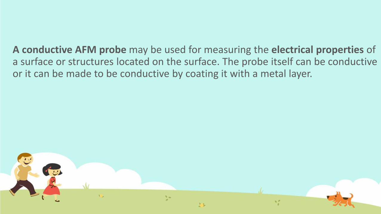
A conductive AFM probe may be used for measuring the electrical properties of a surface or structures located on the surface. The probe itself can be conductive or it can be made to be conductive by coating it with a metal layer.

Electrical mode is very much simple to implement but obtaining reliable data is cumbersome. And following are the problems associated with it : -
1. An oxide layer can build up on the tip or surface making the measurement unreliable.
2. If the probe is coated with a metal, the metal coating can be removed when the probe contacts the surface.
3. The measurements are typically made on materials that are coated with contamination, and getting a reliable electrical contact is difficult.


The previous figure illustrates a probe in the proximity of a sample’s surface and the layers of oxide and contamination that cause uncertainty in AFM electrical measurements.
The oxide layers and contamination make it difficult to make an ohmiccontact between the probe and surface.

One approach to solving issues 1 and 2 is to coat the probe with aconductive diamond coating.
The diamond coating is very hard and does not oxidize. However, the coating increases the diameter of the probe significantly. Even when the probe is coated with an inert layer such as diamond, there are still potential problems for contamination.

Parametric Testing (I/V and C/V)

An electrically conductive probe may be used directly for parametric testing (previous fig).
The parametric tester is attached directly between the conductive AFM probe and the sample.
When measuring I/V curves, a current-limiting resistor is often required to prevent the probe tip from being destroyed by too much current.
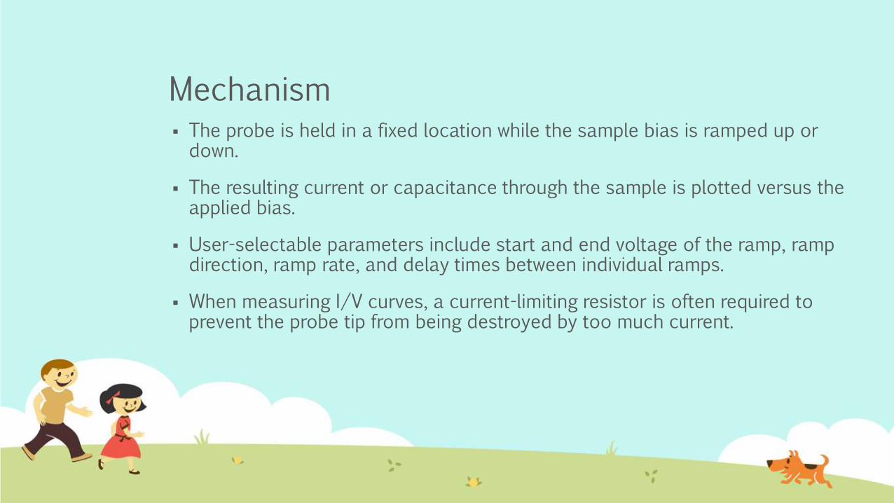
Mechanism The probe is held in a fixed location while the sample bias is ramped up or down.
The resulting current or capacitance through the sample is plotted versus the applied bias.
User-selectable parameters include start and end voltage of the ramp, ramp direction, ramp rate, and delay times between individual ramps.
When measuring I/V curves, a current-limiting resistor is often required to prevent the probe tip from being destroyed by too much current.
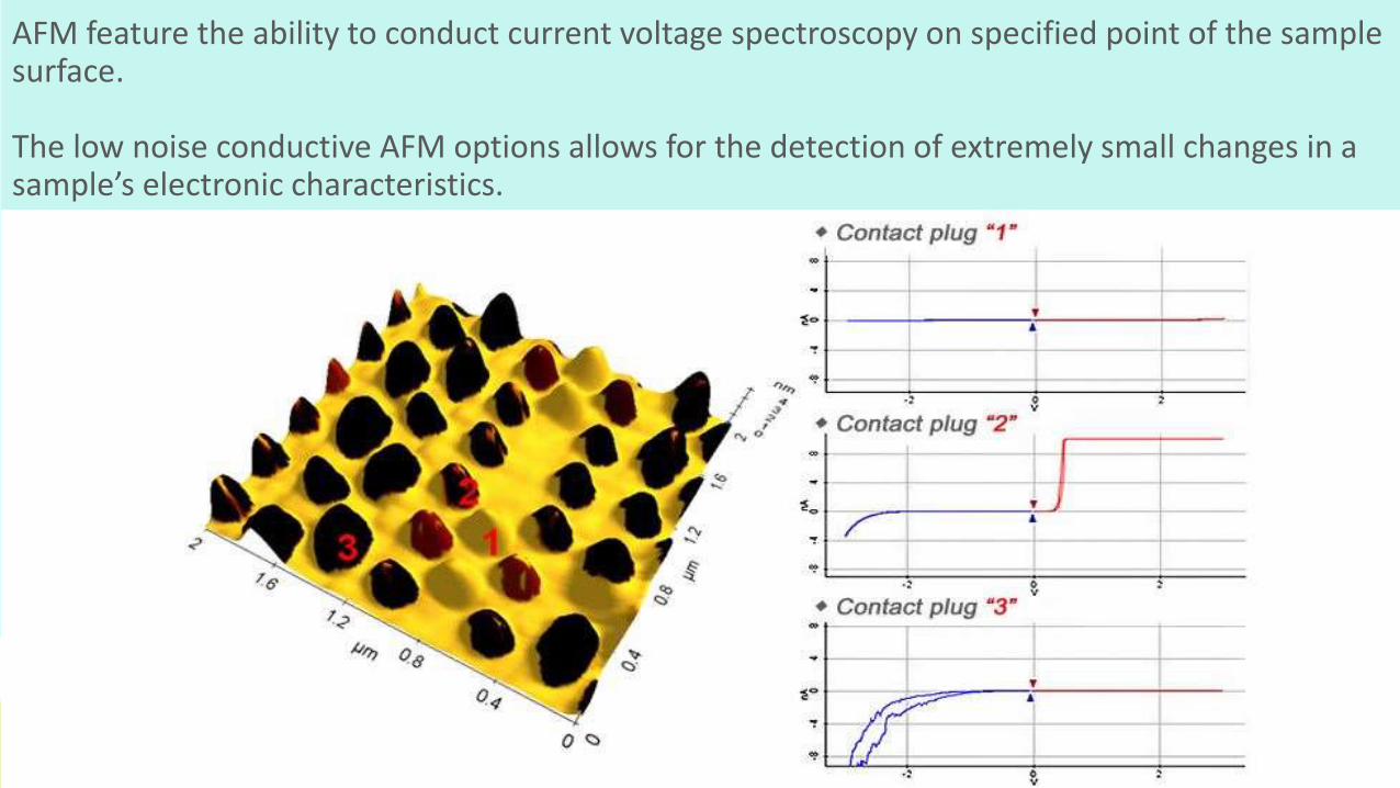
AFM feature the ability to conduct current voltage spectroscopy on specified point of the sample surface.
The low noise conductive AFM options allows for the detection of extremely small changes in a sample’s electronic characteristics.

Using a cantilever as a nanometer scale contact, I-V spectroscopy provides a plot of the current (I) as a function of the tip bias voltage (V) applied to a sample. In order to investigate the electrical properties of the sample surface, I/V spectroscopy is measured on the selected sample area after taking a sample image.

The dI/dV signal can provide information about the surface LDOS (Local density of states ).

The interaction force will be the electrostatic force between the biased tip andsample. However, in addition to the electrostatic force, the van der Waalsforces between the tip and the sample surface are always present. Themagnitude of these van der Waals forces change according to the tip-sampledistance, and are therefore used to measure the surface topography.

The equation for electrostatic forces between a probe and a surface having different potentials is given by -

Applications –measurement of Electrical Properties of nanostructure, nanotube or quantum dots etc.
In addition to the problems discussed earlier, there is another major drawback , i.e, positioningof the AFM scanner over the feature that has only a few nm in diameter.
And the absolute positioning accuracy of an AFM scanner is limited by thermal drift in the stage.

Thank You !!!