Advances in nanowire bioelectronics - Lieber Research …cml.harvard.edu/assets/Zhou_2017.pdfReview...
29
1 © 2016 IOP Publishing Ltd Printed in the UK Reports on Progress in Physics 1. Introduction Bioelectronics generally involves the development and appli- cation of electronics to interface and interact with biologi- cal systems such as biomolecules, cells, tissues, and animal/ human bodies [1]. Since Luigi Galvani’s famous discovery of ‘animal electricity’ from dead frog’s muscles with an electri- cally charged metal scalpel in 1780s, the continuous progress of instrumentation and methodology in bioelectronics has fostered the fundamental understanding of electrical signaling principles for different biological systems from the cellular and subcellular levels [2–5] to the level of cellular networks and tissues [6–9]. In addition to fundamental scientific stud- ies, the development of bioelectronics also has significantly impacted on many healthcare applications. One direction is to advance implantable bioelectronics devices for real-time mon- itoring or regulation of human physiological environments, such as implantable glucose sensors [10], cardiac pacemak- ers [11, 12], cardioverter-defibrillator [13, 14], and deep-brain stimulators [15]. Another direction is towards the develop- ment of on-chip bioelectronics systems that can perform bio- chemical and cell biology analyses for point-of-care medical diagnostics, drug discovery, and disease modelling [16, 17]. In analogue to conventional bioelectronics constructed at the micrometer scale, reducing the dimension of electrical transducers to the nanometer scale can significantly improve the performance. For example, reduction in size can increase the power efficiency, response time and scalability as well as allowing for multi-functional platforms. More uniquely, aggressive miniaturization of transducers down to sub- micrometer and nanometer scale, especially using bottom-up synthesized building blocks, can enable precise one-to-one coupling between bioelectronics devices and individual bio- logical entities at cellular, subcellular, or even molecular level, Advances in nanowire bioelectronics Wei Zhou 1 , Xiaochuan Dai 2 and Charles M Lieber 2,3 1 Bradley Department of Electrical and Computer Engineering, Virginia Tech, Blacksburg, VA 24061, USA 2 Department of Chemistry and Chemical Biology, Harvard University, Cambridge, MA 02138, USA 3 Harvard John A. Paulson School of Engineering and Applied Sciences, Harvard University, Cambridge, MA 02138, USA E-mail: [email protected] and [email protected] Received 18 July 2016 Accepted for publication 6 September 2016 Published 8 November 2016 Abstract Semiconductor nanowires represent powerful building blocks for next generation bioelectronics given their attractive properties, including nanometer-scale footprint comparable to subcellular structures and bio-molecules, configurable in nonstandard device geometries readily interfaced with biological systems, high surface-to-volume ratios, fast signal responses, and minimum consumption of energy. In this review article, we summarize recent progress in the field of nanowire bioelectronics with a focus primarily on silicon nanowire field-effect transistor biosensors. First, the synthesis and assembly of semiconductor nanowires will be described, including the basics of nanowire FETs crucial to their configuration as biosensors. Second, we will introduce and review recent results in nanowire bioelectronics for biomedical applications ranging from label-free sensing of biomolecules, to extracellular and intracellular electrophysiological recording. Keywords: nanowire, bioelectronics, biosensor, field-effect transistor, electrophysiological recording, nanotechnology (Some figures may appear in colour only in the online journal) Review 0034-4885/17/016701+29$33.00 doi:10.1088/0034-4885/80/1/016701 Rep. Prog. Phys. 80 (2017) 016701 (29pp)
Transcript of Advances in nanowire bioelectronics - Lieber Research …cml.harvard.edu/assets/Zhou_2017.pdfReview...

1 © 2016 IOP Publishing Ltd Printed in the UK
Reports on Progress in Physics
W Zhou et al
Printed in the UK
016701
RPPHAG
© 2016 IOP Publishing Ltd
80
Rep. Prog. Phys.
ROP
0034-4885
10.1088/0034-4885/80/1/016701
1
Reports on Progress in Physics
1. Introduction
Bioelectronics generally involves the development and appli-cation of electronics to interface and interact with biologi-cal systems such as biomolecules, cells, tissues, and animal/human bodies [1]. Since Luigi Galvani’s famous discovery of ‘animal electricity’ from dead frog’s muscles with an electri-cally charged metal scalpel in 1780s, the continuous progress of instrumentation and methodology in bioelectronics has fostered the fundamental understanding of electrical signaling principles for different biological systems from the cellular and subcellular levels [2–5] to the level of cellular networks and tissues [6–9]. In addition to fundamental scientific stud-ies, the development of bioelectronics also has significantly impacted on many healthcare applications. One direction is to advance implantable bioelectronics devices for real-time mon-itoring or regulation of human physiological environments,
such as implantable glucose sensors [10], cardiac pacemak-ers [11, 12], cardioverter-defibrillator [13, 14], and deep-brain stimulators [15]. Another direction is towards the develop-ment of on-chip bioelectronics systems that can perform bio-chemical and cell biology analyses for point-of-care medical diag nostics, drug discovery, and disease modelling [16, 17].
In analogue to conventional bioelectronics constructed at the micrometer scale, reducing the dimension of electrical transducers to the nanometer scale can significantly improve the performance. For example, reduction in size can increase the power efficiency, response time and scalability as well as allowing for multi-functional platforms. More uniquely, aggressive miniaturization of transducers down to sub-micrometer and nanometer scale, especially using bottom-up synthesized building blocks, can enable precise one-to-one coupling between bioelectronics devices and individual bio-logical entities at cellular, subcellular, or even molecular level,
Advances in nanowire bioelectronics
Wei Zhou1, Xiaochuan Dai2 and Charles M Lieber2,3
1 Bradley Department of Electrical and Computer Engineering, Virginia Tech, Blacksburg, VA 24061, USA2 Department of Chemistry and Chemical Biology, Harvard University, Cambridge, MA 02138, USA3 Harvard John A. Paulson School of Engineering and Applied Sciences, Harvard University, Cambridge, MA 02138, USA
E-mail: [email protected] and [email protected]
Received 18 July 2016Accepted for publication 6 September 2016Published 8 November 2016
AbstractSemiconductor nanowires represent powerful building blocks for next generation bioelectronics given their attractive properties, including nanometer-scale footprint comparable to subcellular structures and bio-molecules, configurable in nonstandard device geometries readily interfaced with biological systems, high surface-to-volume ratios, fast signal responses, and minimum consumption of energy. In this review article, we summarize recent progress in the field of nanowire bioelectronics with a focus primarily on silicon nanowire field-effect transistor biosensors. First, the synthesis and assembly of semiconductor nanowires will be described, including the basics of nanowire FETs crucial to their configuration as biosensors. Second, we will introduce and review recent results in nanowire bioelectronics for biomedical applications ranging from label-free sensing of biomolecules, to extracellular and intracellular electrophysiological recording.
Keywords: nanowire, bioelectronics, biosensor, field-effect transistor, electrophysiological recording, nanotechnology
(Some figures may appear in colour only in the online journal)
Review
IOP
2017
0034-4885/17/016701+29$33.00
doi:10.1088/0034-4885/80/1/016701Rep. Prog. Phys. 80 (2017) 016701 (29pp)

Review
2
and also, open up device architectures not possible with con-ventional planar fabrication of the semiconductor industry.
Over the last two decades, semiconductor nanowires, either sculptured from top-down or synthesized from bot-tom-up methods, have become a type of ubiquitous build-ing blocks in nanotechnology for vast applications ranging from information technology, energy, to healthcare and life sciences [18–25]. Due to their 1D geometry and prominent surface-to-volume ratio, transducers based on semiconductor nanowires are highly sensitive to detect bioelectrical signals such as biomolecular charges or cell membrane potentials [18, 25–29]. Compared to top-down fabrication methods, bot-tom-up paradigm is particularly attractive due to its versatility to generate semiconductor nanowires with controlled dop-ing/composition profile and advanced geometries (e.g. axial heterostructures, radial heterostructures, branched structures, and kinked geometries) at the stage of synthesis [19, 30–38]. Moreover, the dramatic advances in bottom-up nanowire assembly techniques enable scalable manufacturing of large arrays of nanowire transducers on flexible, biocompatible poly mer substrates that are heat-sensitive and thus incompat-ible to the conventional complementary metal–oxide semi-conductor (CMOS) fabrication process [39–51]. Therefore, semiconductor nanowires, especially those from bottom-up synthesis, are very promising in next-generation bioelectron-ics systems and could potentially open up new opportunities in biomedical applications.
The review starts with a discussion of fundamental aspects related to the preparation, assembly, and electrical properties of semiconductor nanowire devices in the context of bioelec-tronics in section 2. Following this, section 3 will introduce affinity-based nanowire field-effect transistor (FET) biosen-sors for label-free detection of biomolecules. We will discuss methods to improve the performance of nanowire FET sensors in terms of throughput, sensitivity and selectivity as well as how to achieve the detection of biomolecules in high ionic strength physiological environments. Section 4 is focused on the applications of nanowire devices for extracellular electro-physiological recording from cultured cells, ex vivo tissues and organs, 3D engineered tissues, and animal bodies in vivo. Section 5 describes bio-nano interfaces using nanowire sen-sors to access interior of cells for intracellular electrophysi-ological recording. The review ends with conclusions and outlook for future directions.
2. Semiconductor nanowires
Over past two decades, substantial advances in the ‘bottom-up’ synthesis of 1D semiconductor nanowires have enabled precise control of the size, morphology, and chemical compo-sition of these building blocks, thereby enabling many novel nano devices, including nanowire logic circuits [21, 24, 52, 53], memories [54], photodetectors [55, 56], photovoltaic solar cells [23, 57], light-emitting diodes [58], lasers [20, 36] and chemical–biological sensors [18, 59]. Moreover, the bottom-up paradigm allows for the integration of nanowire devices in non-conventional, heat-sensitive and highly-flexible materials
for new applications beyond the capability of current CMOS technology.
2.1. Preparation of semiconductor nanowires
Semiconductor nanowires can be created by a variety of tech-niques, which can be generally categorized in either top-down or bottom-up paradigms. In the top-down approaches, bulk semiconductor materials are sculpted into the nanowires in a subtractive fashion. The geometry and physical properties of top-down nanowires can be accurately controlled through a series of fabrication processes developed in the semicon-ductor industry, including lithographic patterning, reactive ion etching and ion-implantation [60]. Depending on the pur-pose of an application, one can choose to fabricate horizontal nanowires lying in the substrate plane or vertical nanowires perpendicular to the substrate using different top-down pro-cessing protocols. For more details of top-down approaches used to fabricate semiconductor nanowires and devices, read-ers are kindly referred to references [61, 62].
Bottom-up approaches to nanowire synthesis feature an additive self-assembly process of individual atoms and mol-ecules. Thus, bottom-up approaches enable the potential for simultaneous control of geometric shapes and atomic com-position distributions during nanowire growth [32, 33, 35, 37, 63], which can lead to entirely new device concepts and applications beyond the limits of top-down technologies [22, 29, 36, 54, 64, 65]. Among various methods used to generate bottom-up semiconductor nanowires, nanocluster-catalyzed vapor–liquid–solid (VLS) growth has become one of the most powerful strategies because of its simplic-ity and versatility. The VLS mechanism was first proposed by Wagner and Ellis in 1964 to explain vapor phase growth of micrometer scale silicon whiskers [66]. However, it took more than 30 years to create truly nanometer scale semiconductor nanowires, when the Lieber group [30] and Lee group [31] reported the bottom-up synthesis of Si nanowires using laser ablation technique in 1998. In the work by Lieber group [30], laser ablation was used to prepare nanometer-diameter cata-lyst clusters and subsequently facilitate VLS growth of high-quality single crystalline Si and Ge nanowires with diameters down to sub-10 nm. In parallel, Lee and co-workers reported a high-temperature laser ablation approach (1200 °C) to create Si nanowires with diameters ranging from 3 to 43 nm without using metal catalysts. These early demonstrations opened up significant opportunities in the fields ranging from materials science, to energy, and to biotechnology, and led to a dramatic growth of research activities on semiconductor nanowires until now [67–73].
In the VLS mechanism, a metal nanocluster forms a liq-uid alloy at an temperature above the eutectic point for metal and one or more of the elements in the desired nanowire, and as vapor-phase precursor of the targeted nanowire material is added this liquid alloy becomes supersaturated and undergoes nucleation to form a liquid/solid interface from which direc-tional growth of semiconductor nanowires occurs [71, 74, 75]. To achieve VLS growth of semiconductors, the proper growth
Rep. Prog. Phys. 80 (2017) 016701

Review
3
temperature is chosen according to the phase diagram so that the alloy of metal catalyst and nanowire material is in liquid phase while the nanowire material of semiconductor is in the solid phase. The metal catalyst serves as a decomposition-absorption site to transform the nanowire reactant material from the vapor-phase precursor into the liquid alloy seed, and at the same time confines the supersaturation-nucleation site to induce the directional growth of crystalized semiconductor nanowires. The diameter of semiconductor nanowires can be easily defined by using different sizes of the metal catalyst clusters.
2.2. Advanced nanowire structures
The past two decades have seen a rapid advancement in designed, controlled growth of semiconductor nanowires with multiple components and tunable morphologies using the bottom-up paradigm [30]. Beyond the basic type of nanowires with straight shapes and homogeneous composi-tion, researchers have demonstrated four general types of advanced nanowire structures: axial modulated nanowires, radial/coaxial modulated nanowires, branched nanowires, and kinked nanowires (figure 1(A)) [32–37, 58, 63, 74–86]. These advanced semiconductor nanowire structures offer unique opportunities for biomedical applications at the interface with cells and tissues.
In 2002, three research groups demonstrated controlled bottom-up growth of axial modulated heterostructures of InAs/InP [76, 77], GaAs/GaP [32], n-Si/p-Si [32], n-InP/p-InP [32], and Si/SiGe [78] nanowires. To enable a continuous elon-gated growth of axial modulated nanowires, the metal catalyst was chosen in these studies to facilitate reactions with all of reactants under similar VLS growth conditions (figure 1(B)). These seminal reports stimulated exploration of other types of axial modulated nanowire heterostructures, such as axial metal–semiconductor nanowires [83, 87], doping-modulated nanowires [35, 57], and nanowires with ultrashort morph-ology features [88]. A novel extension of these early stud-ies is recent work by Tian and co-workers who reported the creation of axial modulated Si nanowires with additional 3D mesostructures, where the mesostructures are formed by etchant-resistant patterns formed during iterated deposition–diffusion-incorporation of gold within the Si nanowires [86].
In 2002, Lieber and coworkers demonstrated a new radial/coaxial modulated nanowire structure, where a conformal shell was deposited on the surface of the 1D nanowire core [33]. In this work, the authors synthesized and investigated Si and Ge core-shell and multishell nanowire heterostructures using a CVD approach (figure 1(C)). Following this study, the Lieber group demonstrated the growth of other forms of radial/coaxial modulated nanowires including coaxial multilayered (InGaN/GaN)n nanowires [36, 58], radially inhomogeneous core/shell nanowire structures with region-selective and facet-selective shells [85, 89], and diameter-modulated core–shell nanowires through Plateau–Rayleigh crystal growth [38].
Branched nanowires with homo or heterogeneous junc-tions provide a higher degree of complexity to allow for the design of interconnected hierarchical nanostructures with rich electrical, optical, and chemical properties, especially in
energy applications [90]. Various methods have been reported for the synthesis of branched nanowires, such as sequential catalyst-assisted VLS or solution–liquid–solid (SLS) growth, and vapor–solution combination growth [90]. In 2004, Wang et al reported an early demonstration of VLS synthesis of branched Si and GaN nanowires in a controlled manner by sequentially repeating the catalyst deposition and nanowire growth steps (figure 1(D)) [81].
The VLS growth mechanism can also be employed for rational design and synthesis of kinked nanowire structures (figure 1(E)) [37], where kinks are introduced by a perturba-tion in the growth process (e.g. purging or reintroducing reac-tant gases) at defined positions with a fixed angles of 120°. Moreover, by controlling dopant-modulation during kinked nanowire growth process, specific device function, such as p–n diodes and FETs, can be precisely localized at the kinked junctions in the nanowires [91].
The capability to design and create the above mentioned 2D and 3D nanowire structures in a rational manner has opened great opportunities for the design and fabrication unique nanoscale bioelectronics devices to monitor and con-trol nano–bio interfaces. For instance, nanosensors based on kinked nanowires, which will be further discussed in the later sections, can be coated with phospholipid ‘cell-like’ layers to enable tight electrical coupling with cell membranes for intra-cellular recording [29].
2.3. Assembly of nanowires for device fabrication
Since nanowires from bottom–up synthesis typically have dis-ordered arrangement and orientations on the growth substrate (or donor substrate), it is important to explore efficient and large-scale assembly techniques to transfer ordered nanowires with controlled orientation and density on either rigid or flex-ible substrates for subsequent device fabrication. To address this issue, a number of nanowire assembly methods have been reported in the literature, including the Langmuir–Blodgett technique [41, 42], blown–bubble method [92], microflu-idic flow technique [40, 93], electric field-assisted alignment [39, 51, 94], magnetic field-assisted alignment [43], contact printing [45, 92], and recently a nanocombing technique [49].
In 2001, Huang et al demonstrated a microfluidic flow technique to achieve parallel alignment of nanowires up to millimeter length scale [40]. In this method, the angular distri-butions between the aligned nanowires and the flow direction was correlated with the flow rate due to the effects of the shear forces generated by the laminar microfluidic flow. By chang-ing the flow in different directions, higher order hierarchical arrangements of nanowires such as cross-bars and triangles can be realized through layer-by-layer assembly with different flow directions at different steps. In 2007, Yu et al designed a blown–bubble method by blowing homogenous suspension of nanowire-polymer solution into a bubble film with a gas flow and then transferring aligned nanowires from a bubble surface to a substrate during the expansion of the bubble [92]. The separation distance between aligned nanowires can be con-trolled by changing the concentration of NWs in the solution suspension. The blown–bubble method has unique advantages
Rep. Prog. Phys. 80 (2017) 016701
Review
4
for large-area assembly of nanowires from centimeter to meter range on both planar and curved substrates.
In addition to solution-phase nanowire assembly meth-ods, contact printing was reported in 2007 to achieve direct transfer of dry nanowires on substrates for device fabrication [44, 45]. In this method, a dense layer of bottom-up synthesized nanowires is transferred from a growth substrate to a receiver substrate through the directional sliding of the two substrates against each other under a gentle pressure. Importantly, the addition of lubricant between the two sliding surfaces can fur-ther improve the printing alignment of nanowires by reducing uncontrollable breakage of nanowires on the growth substrate during the sliding process [45]. Moreover, deposition of a thin SiO2 buffer layer between adjacent nanowire layers can enable multiple layer contact printing processes with different sliding directions to yield 3D stacked nanowire arrays [44].
Recently, Bang et al reported that it is possible to increase the density of contact-printed nanowire arrays by up to 300% using shrinkable shape memory polymers [50].
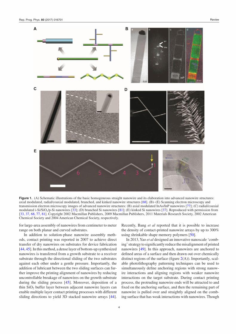
In 2013, Yao et al designed an innovative nanoscale ‘comb-ing’ strategy to significantly reduce the misalignment of printed nanowires [49]. In this approach, nanowires are anchored to defined areas of a surface and then drawn out over chemically distinct regions of the surface (figure 2(A)). Importantly, scal-able photolithography patterning techniques can be used to simultaneously define anchoring regions with strong nanow-ire interactions and aligning regions with weaker nanowire interactions on the target substrate. During contact printing process, the protruding nanowire ends will be attracted to and fixed on the anchoring surface, and then the remaining part of nanowire is pulled over and straightly aligned on the comb-ing surface that has weak interactions with nanowires. Though
Figure 1. (A) Schematic illustrations of the basic homogeneous straight nanowire and its elaboration into advanced nanowire structures: axial modulated, radial/coaxial modulated, branched, and kinked nanowire structures [68]. (B)–(E) Scanning electron microscopy and transmission electron microscopy images of advanced nanowire structures: (B) axial modulated InAs/InP nanowires [77]; (C) radial/coaxial modulated i-Si/SiOx/p-Si nanowires [33]; (D) branched Si nanowires [81]; (E) kinked Si nanowires [37]. Reproduced with permission from [33, 37, 68, 77, 81]. Copyright 2002 Macmillan Publishers, 2009 Macmillan Publishers, 2011 Materials Research Society, 2002 American Chemical Society and 2004 American Chemical Society, respectively.
Rep. Prog. Phys. 80 (2017) 016701

Review
5
nanoscale combing assembly, large-area arrays of parallel NWs with <1° misalignment and with >98.5% yield are pro-duced (figure 2(B)), which enable cost-effective fabrication of large-scale and more sophisticated functional nanoelectronic circuits by the bottom-up approach [24].
In 2000, Smith et al demonstrated electric-field mediated assembly technique [39]. In this method, nanowires sus-pended in a dielectric medium can be individually positioned into specific chip/device locations by alternating electric fields applied between two lithographically defined electrodes. In 2010, Freer et al reported an extended electric-field assembly method to achieve a significant improvement of single nanow-ire assembly yield (98.5%) for 16 000 patterned electrode sites over an area of 400 mm2 with submicron alignment precision [94]. In this method, a solution containing nanowires was injected into a flow channel and then attracted to lithographi-cally patterned electrodes while applying AC electric fields. By carefully balancing the surface, hydrodynamic fluid flow and dielectrophoretic forces, a controllable and self-limiting nanowire assembly process was achieved. However, this method requires a complex fluidic cell coupled with precise control of the flow rate, which could be difficult to implement at wafer scale. To address this issue, in 2015, Collet et al pro-posed an easier and more affordable approach that combines
Figure 2. (A) Schematics of the nanocombing technique for large-area assembly of nanowires. (B) Optical microscopy and SEM images of Si nanowires transferred on the substrate surface by nanocombing process. Reproduced with permission from [49]. Copyright 2013 Macmillan Publishers.
Figure 3. (A) Schematics of capillary-assisted dielectrophoresis technique for wafer-scale assembly of nanowires. (B) SEM images of single Si nanowire FET device made on aligned nanowires by capillary-assisted dielectrophoresis technique. Reproduced with permission from [51]. Copyright 2015 John Wiley & Sons, Inc.
Rep. Prog. Phys. 80 (2017) 016701

Review
6
the dielectrophoresis phenomenon and capillary assembly to align thousands of single nanowires at predefined locations on a wafer scale [51]. In this approach, the liquid meniscus of the nanowire solution is dragged on top of the substrate at a certain velocity and temperature while an AC electric field is applied to the electrodes (figure 3(A)). The assembly of nanowires occurs at the three-phase contact line, where the liq-uid is evaporating to create convective flow inside the solution and thus locally increase the nanowire density at the liquid–air interface. Once a nanowire is attracted by the dielectrophore-sis forces and liquid around the NW evaporates, the nanowire is fixed by the capillary forces at the precise location and with high alignment yield (figure 3(B)).
2.4. Nanowire field-effect transistors
The FET is a 3-terminal semiconductor device that uses an electrical field, which is applied via the third capacitively-coupled electrode, to regulate the electrical conductivity of the semiconductor channel, which is connected to source and drain electrodes [95]. Typically, a gate voltage is applied to control electrostatically the density of charge carriers and thus mod-ulate the conductivity of the channel between the source and drain terminals. Since the gate is insulated from the channel, FET devices have high input impedance. FET devices have been used to transduce different types of charge-based bio-chemical signals, including solution pH, biomolecules, and action poten-tials (APs) [96]. Compared to conventional planar FET devices, nanowire FET biosensors with reduced dimensionality can have enhanced sensitivity because their high surface area-to-volume ratio results in a large electrostatic modulation of car-rier density in the channel by any perturbation of electric fields at the surface. As the nanowire’s diameter is comparable to or smaller than Debye screening length determined by the dopant density in semiconductor, a small perturbation of electric field from a single biomolecule at the nanowire surface can cause a charge accumulation/depletion region deep into the entire nanowire and thus substantially change the current flow in the channel [68, 73, 97]. In contrast, the current can flow around the perturbed region in 2D planar channel. Therefore, 1D nanowire FET devices can serve as highly sensitive bioelectronics trans-ducers for in vitro and in vivo applications.
For applications related to chronic in vivo cell-recording, nanowire FET transducers also need to have long-term sta-bility in physiological environments. Some previous studies reported the dissolution of nanoscale Si materials/devices under physiological conditions with or without cell culture in various times between 1 and 3 weeks [27, 98, 99]. Although the native SiO2 layer on the Si nanowire device is stable in the dry state [100], it can be dissolved by hydrolysis in aqueous solutions with a dissolution rate proportional to ionic strength and thus faster in physiological environments [101, 102]. The dissolution of Si structures occurs by a cycle in which the silicon surface is continuously re-oxidized and dissolved. Different stabilities reported by previous studies may be attrib-uted to the complexity of nanostructure/cell interfaces where protein adsorption and/or lowered oxygen concentrations can substantially slow dissolution and/or reoxidation steps.
In 2014, Zhou et al demonstrated that the intrinsic long-term stability of semiconductor nanowire FET devices (30 nm in diameter) in physiological environments can be improved from less than 10 days to over 100 days with a 10 nm thick conformal Al2O3 shell coating by atomic layer deposition (ALD) technique [103]. Al2O3 was chosen as the nanowire protective shell material in this study for several reasons. First, Al2O3 has excellent chemical stability in the physiological environ ments, and, has been used as a biocom-patible material for implanted dental and orthopedic applica-tions [104]. Second, the Al2O3 shells should not adversely affect the performance of nanowire FETs since Al2O3 is a high dielectric constant gate material [105]. Third, it is easy to achieve high-quality, pinhole free, conformal shells of Al2O3 on nanowires with accurate control of thickness in the nanometer scale by ALD technique [106].
3. Label-free detection of biomolecules
Progress for point-of-care testing depends on the develop-ment of miniaturized, portable and/or handheld biomedical diagnostics devices with high sensitivity, high throughput, easy operation, and low maintenance. Because of the high surface-to-volume ratio, comparable dimension to biomol-ecules, and available surface chemistry methods for selec-tive molecular interactions, nanowire FET biosensors have been extensively investigated for real-time, label-free detec-tion of a variety of biomolecule disease markers, such as proteins [25, 107–110], nucleic acid [111–117], and viruses [118–120]. Furthermore, nanowire FETs have been applied to characterize interactions between different biomolecules [26, 108, 109], which are crucial for applications in drug screening and investigating basic biophysical properties. Significantly, the integration of large arrays of individually addressable nanowire FET biosensors for multiplexed detec-tion, the compatibility of nanowire FET devices with micro-fluidic systems, and the requirement of only a small amount of sample solution for biomedical testing, have already been demonstrated as milestones towards important clinical appli-cations [59, 71, 72, 121–123].
The typical structure of nanowire biosensors for biomol-ecule detection is illustrated in figures 4(A) and (B), where the channel region in a Si nanowire between the source and the drain contacts serves as the active sensing component. In order to selectively recognize biomolecule targets in solution, the channel surface of the nanowire FET is functionalized with biomolecule receptors, such as antibodies or single-strand deoxyribonucleic acid (DNA) probes. The perturbation of electric potential at the nanowire FET surface associated with binding events of charged biomolecules (the sign and quantities of their charges depend on the isoelectric point of the biomolecules and the solution pH) leads to a change of the charge carrier density and conductance of nanowire FET devices in real time. By integrating a number of these nanow-ire FETs functionalized with different receptors on a single chip, a powerful platform for multiplexed chemical/biological recognition can be achieved (figure 4(C)) [26, 124].
Rep. Prog. Phys. 80 (2017) 016701

Review
7
3.1. Surface functionalization
For semiconductor nanowires (e.g. Si, ZnO, and In2O3 nanow-ires) with a surface oxide layer, the presence of surface ter-minated hydrophilic hydroxyl group can be used to generate active functional amine, thiol, or aldehyde groups on the sur-faces of nanowires for a subsequent covalent attachment of bioreceptors by using alkoxysilane derivatives [18, 118, 125].
An early example of surface functionalization to yield Si nanowire FET pH sensor was achieved by modifying the native oxide layer with 3-aminopropyltriethoxysilane (APTES), which presents amino groups (–NH2) at the NW/solution interface (figure 5(A)) [18]. Variations in the hydro-gen ion concentration will result in protonation and deprot-onation of the amino and silanol groups (Si–OH) on the oxide layer, and consequently modulate the surface charges and NW conductance (figure 5(B)) [18]. The presence of native surface oxide and additional siloxane layer from function-alization process does increase the effective thickness of the insulator layer between gate and channel, and may degrade the sensitivity and detection limit of nanowire FET sensors. To mitigate this issue, Bunimovich et al proposed to chemi-cally remove the surface oxide with diluted hydrofluoric acid and then use UV-assisted photohydrosilylation to functional-ize hydride terminated surface (Si–H) with olefin derivatives
[120]. The authors reported a 100 fold improvement in the detect limit, although it is unclear all factors that led to this improvement [126].
In additional to chemical functionalization by covalent bonding, biomolecules can also be immobilized on the sur-face of biosensors by the physical adsorption. Physical immo-bilization approaches are, however, limited by several issues, including difficulties in controlling biomolecule immobiliza-tion, low bio-receptor activity, and desorption of biomolecule receptors after immobilization [123]. More recently, Noy et al demonstrated that it is possible to integrate functional lipid bilayer membrane mimicking the cell membrane on the sur-face of nanowire FET devices to monitor bioelectrical signals [127]. With lipid bilayers containing transmembrane peptide pores, the FET devices can transduce ionic pH signals into electronic conductance signals by using voltage-gated or chemically gated ion transport through the membrane pores.
3.2. Selectivity and multiplexed detection
The selectivity of a sensor reflects its ability to measure a con-centration of a targeted analyte in the presence of other inter-fering substances. The selectivity of nanowire biosensors is realized by immobilizing receptor molecules on the nanowire
Figure 4. (A) (left) Schematic illustration of a nanowire FET configured as a sensor with antibody receptors (blue). (right) Binding of a protein with a net negative charge to a p-type nanowire yields an increase in conductance. (B) Schematic of a prototype nanowire sensor biochip with integrated microfluidic sample delivery. (C) Schematic of a nanowire sensor array for multiplexed, real-time sensing of multiple biological species. Reproduced with permission from [97]. Copyright 2007 Materials Research Society.
Rep. Prog. Phys. 80 (2017) 016701

Review
8
surface, and the immobilized receptor molecules are chosen to bind specifically to the targeted analyte molecules. For 1D nanowire biosensors with a very small footprint, even a small degree of non-specific binding of non-targeted molecules to the receptor molecules can significantly degrade the selectiv-ity due to binding competition [18, 25, 109, 128]. To miti-gate the issue of nonspecific binding, a general method is to block the remaining active sites on the surface of biosensors with a layer of hydrophilic molecules, such as bovine serum albumin (BSA) [18], and poly(ethylene glycol) (PEG) [124, 129], which have low protein adsorption character-istics. For label-free detection of DNA by nanowire FET devices, Gao et al recently applied rolling circle amplifica-tion (RCA) to achieve selective signal enhancement with reduced nonspecific binding owning to the dominant bind-ing of large amount of repeated sequences of RCA products [130]. Furthermore, simultaneous detection of target mole-cules by both n-type and p-type nanowire FET devices were used to rule out the false signal attributed to the nonspecific binding or other noises [26].
For many practical diagnostic applications, it is desirable to achieve multiplexed detection by differentiating different types of analyte molecules and their concentrations in com-plex media containing different biomolecules, such as blood and other body fluids. For example, simultaneous detection of 3–5 biomarkers is typically required to establish reliable diag-nosis of a complex disease such as cancer [131]. Moreover, multiplexed detection with a large array of nanowire biosen-sors immobilized with different receptors can help to mitigate possible cross-selectivity of receptors towards other types of interfering analyte molecules by evaluating the overall vector pattern of responses from multi-receptor sensor arrays [121]. In 2005, Zheng et al demonstrated that nanowire FET biosen-sors allowed label-free, real-time and multiplexed detection of three cancer marker proteins, PSA-α1-antichymotrypsin, carcinoembryonic antigen, and mucin-1, achieving detection limits to at least 0.9 pg ml−1 in undiluted serum samples [26].
An array of both p-type and n-type silicon-nanowire FET devices was incorporated in a single sensor ship, and was then bonded to a microfluidic channel made of a PDMS for bio-logical sample delivery. Experiments showed that Si nanow-ire FETs modified with different PSA biomarker receptors (including PSAα1, CEA, and mucin-1) can produce differ-ent signal traces (in term of the conductance change) propor-tional to the concentrations of the different biomarkers. More recently, Zhang et al reported a multiplexed detection of three cardiac biomarkers (including cTnT, CK-MM, and CK-MB) in serum using 40 clusters of 200 independently addressable Si nanowire FET sensors interfaced by a readout application specific integrated circuit (ASIC) [124]. The incorporation of the ASIC helps to reduce the effect of cross channel coupling and enable simultaneous detection of different bio-molecules at a frame rate of kilo-samples per second.
3.3. Sensitivity and detection limit
In order to detect extremely small signals such as the bind-ing of a single molecule or the extracellular electrical poten-tial from a single cell, significant efforts have been directed toward understanding factors affecting the sensitivity and detection limit of nanowire biosensors. For the operation of nanowire FET biosensors, the binding event of a charged spe-cies to the nanowire surface modified with receptor molecules will be converted into a change in drain-to-source current (ΔI) or conductance (ΔG) because of a change in nanowire surface potential.
The sensitivity and the detection limit of nanowire FET devices are determined by the signal-to-noise ratio (SNR), which depends on the transconductance of nanowire FET devices as well as the intrinsic FET device noise and extrin-sic instrument and environment noise. Recently, it has been shown that the main sources of noise are related to the intrin-sic device fluctuation owning to the electron scattering process [133]. Thus, the SNR can be enhanced by the optimization of
Figure 5. (A) Schematic illustration of pH sensing by a nanowire FET device. (B) Real-time detection of the conductance for an APTES-modified SiNW for pHs from 2 to 9. (inset, bottom) SEM image of a typical Si nanowire FET device. Reproduced with permission from [18]. Copyright 2001 American Association for the Advancement of Science.
Rep. Prog. Phys. 80 (2017) 016701

Review
9
the device [134, 135]. Moreover, recent experiments show that the current noise is independent of electrolyte concentration, composition, or pH [133].
Li et al experimentally investigated the effect of nanowire diameter, doping density and nanowire number on the sensi-tivity of nanowire FET devices [136]. The study demonstrated that the device sensitivity decreased with the increasing number of nanowires owning to the competitive binding and depletion of analyte molecules in the surrounding solution. Moreover, nanowires with a lower doping density or a smaller diameter were observed to produce a larger transconductance and a higher detection sensitivity because of the increased electrostatic control of the carrier density in the channel.
Other than the intrinsic characteristics of nanowires, the sensitivity of nanowire FET biosensors is also influenced by the operation mode and configuration. Traditionally, nanow-ire FET biosensors are operated in the linear regime above the threshold voltage, where the transconductance varies lin-early with the surface potential. In 2010, Gao et al demon-strated that the sensitivity of nanowire FET sensors can be enhanced in the subthreshold regime where the transconduct-ance depends exponentially on the surface potential induced by bound molecules [132]. In the subthreshold (depletion) regime (figure 6(A)), the low carrier density in nanowires results in a screening length λSi larger than the diameter of nanowires, and thus the field effect of surface charges can
gate the whole nanowire, fully utilizing the high surface volume ratio of nanowire. This principle is exemplified in both pH- and protein-sensing experiments, in which a liquid gate is applied as a reference to tune the operational mode of nanowire FETs. pH sensing experiments were used to study the sensitivity of nanowire FET sensor in both linear and sub-threshold regimes, where the silicon oxide surface of nanowires was modified with (3-aminopropyl)triethox-ysilane. When the pH of electrolyte solution is varied, prot-onation/deprotonation of amino (–NH2) and silanol (Si–OH) groups modulates the surface potential and thus results in the change of conductance in nanowires. Real time pH sens-ing data in figure 6(B) shows a much larger modulation of normalized signal (ΔG/G) in the subthreshold regime than in the linear regime. Figure 6(C) illustrates real-time sens-ing of PSA/antibody interaction by nanowire FET biosen-sors, where a much higher SNR was also achieved in the subthreshold region compared to the linear region simply by adjusting the bias voltage of the liquid gate. One condition to achieve high detection limit for nanowire biosensors in sub-threshold regime is that intrinsic device noise from carrier scattering in the channel dominates the overall noise for the sensing signals. If the main source of noise is attributed to other mechanisms, such as trapping states on nanowire sur-face, or Schottky-barrier at the interface between nanowire and metal contact, current injection and/or interface trapping/
Figure 6. Nanowire FET sensing in subthreshold region. (A) Conductance G versus electrolyte gate voltage Vg of a p-type Si nanowire FET. The inset shows the schematic of electrolyte gating. This device has a transconductance of ~700 nS V−1 in the linear regime and subthreshold slope S ~ 180 mV/decade in the subthreshold regime, with a threshold voltage VT ~ 0 V. (B) Real time pH sensing plotted as the percentage change, ΔG/G, with the conductance value at pH = 4 as the reference point. In the subthreshold regime (Vg = 0.2 V), the device shows much larger percentage change in conductance as solution pH changes. (C) Comparison of real-time sensing of PSA/antibody conjugations by NW FET sensor with the gate voltage being changed from linear (Vg = 0 V) to subthreshold regime (Vg = 0.45 V). Reproduced with permission from [132]. Copyright 2010 American Chemical Society.
Rep. Prog. Phys. 80 (2017) 016701

Review
10
detrapping, then the exponential dependence of conductance on gate voltage/surface potential in the subthreshold regime may not necessarily result in enhanced SNR [132].
In 2010, Ahn et al proposed a double-gate nanowire FET biosensor which has separated double-gates sitting vertically on the Si nanowire and face each other [137]. Compared to conventional nanowire FET biosensor with a single back gate, the conduction channel in double-gates FET device can be precisely controlled by the bias voltages from the two gates. By tuning the two gate voltages, a double-gates FET device can operate in the subthreshold region and show a higher sen-sitivity compared to the single gate nanowire FET with the same nanowire dimensions.
Conventionally, FET biosensors measure the total electri-cal signals in real time. Zheng et al recently demonstrated a new biomolecule detection methodology though frequency domain analysis of measured electrical signals using Si nanowire FET biosensors [138]. In this method, the pertur-bation of carrier transport in the device due to the dynamic interaction between biomolecule and nanowire surface can be differentiated by identifying a Lorentizian peak shape in kilohertz frequency range over the 1/f noise background in the measured power spectrum. This work carried out a side by side comparison study between the time domain and frequency domain measurements of antigen concentration changes in the fluid based on the same device, which showed a more-than 10-fold increase in detection sensitivity in the frequency domain measurement. Therefore, the frequency domain anal-ysis provides a powerful approach complementary to the real-time detection especially when the extrinsic noise level is high or the system investigated is in an equilibrium state.
3.4. Detection in physiological solutions
Accurate and rapid analysis of biomolecules in physiological solutions is crucial for clinical disease diagnosis and treatment [139]. The nanowire FET device is one of the most promis-ing platforms for real-time, label-free, and multiplexed sens-ing of bimolecular species. However, the ability of nanowire FET sensors to detect charged biomolecules in physiological liquids with a high ionic strength is significantly hindered by Debye screening effects [140, 141]. In ionic solutions, the sur-face charge attracts counterions to create an electrical double layer that effectively screens off the electric fields from the surface charges. The thickness of the electrical double layer is characterized as the Debye length, λD, describing a distance from a surface charge where the surface potential exponen-tially decays to 1/e of its initial value. λD is dependent on the ionic strength of a solution, and is given by
k T
N q I2D
B
A2
λε
=
where ε is the dielectric permittivity of the solution, kB is Boltzmann’s constant, T is the temperature, NA is the Avogadro number, q is the elementary electron charge, and I represents the ionic strength of the solution. For common physiological solution samples (i.e. blood, serum, and urine),
λD is approximately 0.7–2.2 nm, and thus nanowire FET sen-sors exhibit poor sensitivity to detect large biomolecules in physiological solutions where the surface potential will be completely screened at a distance of a few nanometers. To overcome the limitation of the Debye screening, several indi-rect and direct methods have been developed to detect blood/serum samples in a controlled manner.
An early indirect approach employs an initial ‘desalting’ step to achieve detection of blood serum disease marker pro-teins in low ionic strength buffers [26]. In this method, the serum samples were first desalted using a centrifuge filter and then diluted back to the original protein concentration with the assay buffer solution before injection into the detection system. A second indirect method applies a microfluidic puri-fication chip system to catch the cancer marker molecules from physiological solutions, and then to wash and release the antigens into a pure low-ionic strength buffer suitable for sensing by nanowire FET devices [142]. These two indirect methods share a similar strategy by using a two-stage process to isolate the target molecules from physiological environ-ments of high ionic strength and then release them into diluted low ionic solutions for FET sensing. Such approach can help to mitigate the challenges from Debye screening effects and alleviate other issues such as biofouling and nonspecific binding in complex physiological samples. A third indirect method involves a steady-state measurement rather than a real-time detection [124], in which sensing response is meas-ured by monitoring the resistance change after protein bound to the antibody anchored on the Si nanowire sensor surface. Particularly, the first resistance value of the nanowire sen-sor is measured in a low ionic strength buffer solution after immobilization of antibody, and the second resistance value is recorded in the same measuring buffer solution after the nanowire sensor undergoes incubation with undiluted serum and subsequent washing. This method is independent of the ionic strength of the sample solution, thus is not limited by the Debye screening effects in physiological solutions.
While effective, these indirect methods require the opera-tion in low-concentration ionic solutions and often use time-consuming or complicated sample treatment process, which hampers their applications for many types of in vitro and in vivo detection. Moreover, since the ionic strength of most physiologically relevant samples is ⩾100 mM, it is crucial to find direct ways to overcome Debye screening effects both for proteomics studies in physiological conditions, and for real-time clinical point-of-care analysis, where the detection of very small sample volumes with very low concentrations of target biomolecules is required.
The first direct approach was proposed to detect biomol-ecules within the Debye length in undiluted serum and blood samples using small fragments of antibody-capturing units [143]. In this approach, the sizes of antibody-capturing spe-cies are reduced by bioengineering methods to make the bound biomolecules in closer proximity to the nanowire sur-face, and thus the detection limit of nanowire FET sensors can be enhanced owning to a stronger electrostatic control of nanowire channel carriers by the bound biomolecules. Interestingly, it was observed that lower antibody fragment
Rep. Prog. Phys. 80 (2017) 016701

Review
11
surface coverage results in a higher detection limit for nanow-ire FET devices under the high ionic strength conditions, indi-cating a correlation between nanowire device sensitivity and receptor dimensions.
A second direct approach for biomolecule detection in high ionic strength solutions is based on a high-frequency measurement strategy [144]. In this method, nonlinear mix-ing between the excitation field from the alternating current in a carbon nanotube FET device and the dipole field of bound molecules can generate signals of mixing current that depends on the numbers of bound biomolecules on the device surface. With increasing frequency, the impedance of electrical double layer on device surface decreases and AC electric field pen-etrates deeper into the solution to drive the dipoles of bound biomolecules. Therefore, at high frequencies, the excited dipoles can modulate the carriers in the FET channel to gener-ate a mixing conductance response much higher than the low frequency response of device limited by Debye-screening. This work experimentally demonstrated electrical detection of monolayer streptavidin binding to biotin in 100 mM buffer solution at a frequency beyond 1 MHz.
In 2015, Lieber and co-workers proposed a new direct strategy for real-time detection of biomolecules in physi-ological solutions using nanowire FETs [145]. This method involves linking a porous and biomolecule permeable polymer to the surface of the FET such that the effective Debye length is increased, which enables direct real-time detection of pro-teins and other biological analytes in physiology-relevant high ionic strength environments. Specifically, a biomolecule- permeable polymer layer prepared from a mixture of PEG and (3-aminopropyl)-triethoxysilane (APTES) on the nanowire FET sensor surface can reduce ion concentration and increase Debye length near the nanowire FET surface (figures 7(A) and (B)). Using prostate specific antigen (PSA) as a model sys-tem, APTES/PEG-coated nanowire FETs can detect PSA in phosphate buffer concentrations up to 150 mM, with a detec-tion sensitivity of ~10 nM and linear response range up to 1000 nM. In contrast, similar FETs without PEG functionali-zation can only detect PSA in buffer salt concentrations lower
than 10 mM. This work suggests a new and general device design strategy for the FET sensor applications in physiologi-cal environments, which is applicable for both in vitro and in vivo sensing.
4. Extracellular electrophysiological recording
Electrophysiology investigates vital bioelectrical activities in electrogenic cells and cell networks, such as neurons, cardio-myocytes, and muscle cells [7]. Examples of such bioelectrical processes include: information transmission and processing by neural networks in the brain; visual response to the light through retinal ganglion cells in the eye; and coordinated beating of cardiomyocytes in the heart. To advance further our understanding of complex bioelectrical activities in the human body, there is a strong demand for high spatiotemporal resolu-tion techniques for electrophysiological measurement.
The past decade has witnessed substantial advances in optical approaches for recording and stimulating electrophysi-ological activities in the brain and heart [146–150], especially with the advent of optogenetics [151, 152]. However, optical methods still have several limitations, including difficulty in monitoring activity deep inside tissue and in achieving simul-taneously high spatial and temporal resolution. At the same time, nano-bioelectronics, as a branch of nanotechnology, has also made significant progress in achieving multiplexed, long-term detection of bioelectrical activity with high spatiotempo-ral resolution [73, 153–155].
4.1. Bioelectronics for extracellular electrophysiological recording
The bioelectrical activity of electrogenic cells arises from ion currents flowing across the cell membrane, which simulta-neously changes ion concentrations and electrical potentials both inside and outside the cell. Therefore, direct electrical recording of bioelectrical activity of cells can be implemented in two different fashions: (1) intracellular measurement by reaching the cell interior with a transducer, such as the ‘patch
Figure 7. Polymer surface modification to increase the effective Debye length for FET biosensing. (A) Schematic illustration of a nanowire FET device (top) without and (bottom) with a porous and biomolecule permeable polymer (green) surface modification. The magenta features on both nanowire surfaces represent APTES in these studies, or more generally, specific receptors. (B) The dependence of PSA signal amplitudes and Debye length on the phosphate buffer concentrations, where APTES/PEG corresponds to modification with 4:1 APTES/silane-PEG. Reproduced with permission from [145]. Copyright 2015 American Chemical Society.
Rep. Prog. Phys. 80 (2017) 016701

Review
12
clamp’ micropipette [2, 156]; and (2) extracellular measure-ment using a transducer placed close to the exterior of cell membrane [17, 157, 158]. Compared to intracellular record-ing that requires puncturing the cell membrane, extracellular recording techniques are less invasive, and thus are compati-ble for long-term measurements. Extracellular recording does, however, provide less detailed information about bioelectric activity [159]. Moreover, it is much easier to implement mul-tiplexed electrical recording outside of cell membrane based on arrays of transducers. These extracellular transducers can either be metal microelectrodes, or FETs.
In 1972, Thomas et al reported a planar metal microelec-trode array (MEA) for recording electrical activity from cul-tured heart cells to study plasticity and electrical interaction among the cellular network [8]. Four years later, Pine et al achieved successful recording of APs from dissociated neuron cells using a planar MEA [160]. Such techniques for extra-cellular electrophysiological recording are now referred to as MEAs, and have undergone several improvements over the past couple of decades [17, 161, 162]. In an MEA, each metal electrode can be individually addressed for signal amplifica-tion and processing. This capability makes the MEA a power-ful tool to investigate the spatiotemporal network dynamics both in vitro and in vivo [17, 157, 158, 161, 163–165]. In addition, a metal electrode can also be used to apply a volt-age transient and stimulate electrical activity of nearby cells due to a depolarization of cell membrane. Normally, the size of electrode used for extracellular recording is between 5 µm and 100 µm [166–168]. Although a relatively larger electrode surface ensures a reasonably smaller impedance required for sufficient SNR, it limits the capability for recording signals from subcellular structures, such as axons and dendrites [151]. Moreover, large size electrodes can complicate the interpre-tation of recorded signals because the recorded signals often arise from the contributions of several neighboring cells [167].
As an alternative approach, an open gate FET has also been used as an active transducer for extracellular recording. In the 1970s, Bergveld reported the use of FETs in electrophysiolog-ical applications, such as extracellular recording of ion pulses from a guinea pig taenia coli [169], and measurement of APs from the flexor tibialis muscle of a locust [170]. In 1991, Fromherz et al reported extracellular recording from a neuron cell of the leech [171]. FET based transducers and their arrays can be fabricated by standard CMOS technology. Recently, a 128 × 128 open-gate CMOS FET array was demonstrated for extracellular recording of neural activity [172].
In extracellular recording, all current sources superimpose to generate the electrical potential at any given location, and the contribution of potential from one source scales with the inverse of the distance between the source and recording site. Therefore, the shapes and amplitudes of extracellular signals depend on the relative position of the transducer with regard to the position of ion current sources (cluster of cells, single cell, soma, axon, dendrites), as well as the nature of cells and cellular networks under investigation [9, 173]. Accordingly, the increase of the distance between the recording transducer and a target electrogenic cell will reduce the relevance and the quality of the measured signals with regard to the bioelectrical
activity occurring from that target cell. Analytical methods of electrical cable theory are usually exploited to model extra-cellular potentials and correlation between extracellular and intracellular signals, although with a number of unknown parameters there can be some uncertainty in the conclusions [6, 174]. For example, the interface between the transducer and the cells investigated plays a vital role in extracellular recording and modeling, since it determines the seal resistance of the cleft space on the recording transducer with respect to ion currents [162]. The seal resistance to the leaking ion cur-rents typically increases with reduced cleft distance, and a larger seal resistance can help to improve the SNR to record subtle extracellular voltage signals. The seal resistance can be increased by promoting cell adhesion to the transducer using approaches, such as chemical modification of the transducer surface [171, 175, 176] as well as shape and structure engi-neering of transducers [162, 176–178].
4.2. Recording from cultured cells
Compared to conventional passive metal electrodes and active FET transducers with microscale device dimension, nanow-ire bioelectronics have substantial advantages in achieving nanoscale interfaces between recording transducers and bio-logical systems. Particularly, the nanoscale device footprint enables precise registration for single cell recording and also allows very dense packing of large arrays of transducers in a single device or chip for large-scale multiplexed recording of bioelectrical dynamics in complex cellular networks with high spatiotemporal resolution.
Partly thanks to the maturing of both bottom-up and top-down fabrication process of nanowires and their devices, nanowire FETs have emerged as one of the most promising nanoscale bioelectronics devices for extracellular recording with subcellular resolution [68, 69, 73, 179, 180]. Similar to conventional planar FET transducers, nanowire FETs show conductance change in response to variations of extracellular potential in the cleft space surrounding the 1D active chan-nel in the nanowire. But nanowire FETs are expected to be more sensitive than their planar counterparts because of their device topology and 1D nanoscale morphology; that is, the nanowire protrudes from a substrate surface and can enhance interactions with the cell membrane, and in respond to a same level of extracellular voltage signal, a more thorough deple-tion or accumulation of carriers occurs in the entire ‘bulk’ of the 1D nanowire than in the case of a planar device. As a type of active potential transducer, nanowire FETs simultane-ously convert and amplify extracellular voltage signals to cur-rent signals, and thus their performance is not limited by the high solution-device interface impedance due to the nanoscale device size [95, 181].
In 2006, the Lieber group first demonstrated the use of open gate Si nanowire FETs for extracellular recording from cultured rat cortical and hippocampal neurons [27]. In this work, Si nanowire FET devices were fabricated by a bottom-up paradigm, while all the metal contacts on the chip were passivated for cell culture. With a predefined sur-face patterning of poly-lysine on the nanowire FET device
Rep. Prog. Phys. 80 (2017) 016701

Review
13
chips, the cultured neuron cells were guided to grown with a good alignment on FET device arrays, which helped to ensure a high yield of interfaces between neurons and nanowire FET transducers. In figure 8(A), the extracel-lular neuron signals recorded by a nanowire FET shows a good time correlation with the intracellular APs recorded by a glass micropipette. The inset of figure 8(A) shows an optical image of a good alignment between the nanowire FET device and the recorded axon part of a single cortex neuron. This work demonstrated that nanowire FETs were capable of direct recording of AP signals from individual neurites and other subcellular neuronal structures, which would otherwise be difficult or impossible by conventional microscale transducers due to their large sizes. Figure 8(B) shows a guided neurite growth from a central neuron soma across three of the four peripheral nanowire FET devices positioned in a rectangle array. Results show that only those nanowire FET devices interfaced with the axon (NW1) and dendrites (NW2 and NW3) are able to record signals, while the control device (NW4) with no connection to the neuron does not show any signal. In addition, a multi-site nanow-ire FET array configuration was created to investigate the neuronal signal propagation process, revealing different signal propagation rates of 0.16 m s−1 for the dendrite and 0.43 m s−1 for the axon. Figure 8(C) shows a configuration containing 50 independently addressable nanowire FET devices where the axon from a single neuron was guided to grow across the channel region of 50 nanowire FET devices. Overall, these results show the potential for nanowire FET arrays for multiplexed recording with subcellular spatial resolution from neurons.
Other than cultured neurons, nanowire FETs have also been used for extracellular recording from cultured cardiomy-ocytes [182–184]. In 2009, the group of Chen employed top-down fabricated Si nanowire FETs for extracellular recording of bioelectrical activity from dissociated cardiomyocytes cells [184]. In this work, nanowire sensing regions included 1D array of 100 nanowires with a spacing of 2 µm, a length of 100 µm, and a diameter of 30 nm. The long nanowires were purposefully used to allow measurement across an entire cell membrane of cardiomyocytes or simultaneous measurement from multiple cells. Rhythmic transient changes attributed to an upstroke current spike followed by a downstroke one were observed after cardiomyocytes were cultured on nanow-ire FET chips for 1–2 d. The authors assumed that the paired opposite spikes could be respectively attributed to the onset and shut-off of an AP process. The group of Offenhausser car-ried out extracellular recording of cardiac muscle HL-1 cells with top-down fabricated nanowire FETs, and compared the measured bioelectrical signals with ones from conventional planar FETs [183]. Importantly, the results show that nanow-ire FETs exhibited a higher SNR for extracellular recording than that of the standard planar FET devices as originally sug-gested by the Lieber group [89].
In 2009, Lieber and co-workers reported a flexible method to interface nanowire FETs with cells for extracellular record-ing [182]. In this work, embryonic chicken cardiomyocytes were cultured on thin, optically transparent polydimethylsilox-ane (PDMS) slabs that were then brought into contact with bot-tom-up fabricated nanowire FET arrays on standard substrates for electrophysiological measurements. Stable field potential spikes with high SNRs (>5) were simultaneously recorded
Figure 8. Extracellular AP recording from cultured neurons. (A) Top left: intracellular potential of an aligned cortex neuron (after 6 d in culture) recorded by glass micropipette during stimulation. Bottom left: time-correlated signal from axon measured using a p-type Si nanowire FET. Top right: optical images of a nanowire–neuron interface. (B) Left: optical image of a cortical neuron interfaced to three of the four functional nanowire FETs in an array. Right: trace of intracellular current stimulation and resulting electrical responses from the four Si nanowire FETs. (C) Aligned axon crossing a 50-nanowire device array and corresponding signal propagation data. Reproduced with permission from [27]. Copyright 2006 American Association for the Advancement of Science.
Rep. Prog. Phys. 80 (2017) 016701

Review
14
from multiple nanowire FETs in contact with cardiomyocytes, indicating a good device-cell interface with a large seal resist-ance of the cleft space to the ion currents. In addition, the authors observed that signal strength in the recording increased from an average SNR of 5 to a maximum SNR of 25 by bring-ing the cells closer to devices with a force applied to the PDMS cell culture slab. Importantly, the changes of signal amplitude were reversible and the device–cell interface was stable when a constant force was applied to the PDMS cell culture slab. This method has unique advantages in allowing separate design and optimization of nanowire FET chip and cell culture, as well as enabling precise alignment between device chip and PDMS cell culture slab using optical microscopy. Moreover, it is pos-sible to use this approach to identify and register to targeted cellular and subcellular structures with respect to nanowire FET arrays for high-resolution multiplexed recording.
4.3. Recording from tissues and organs
Tissues obtained from the brain or heart consist of complex 3D cellular networks, and thus represent a more realistic biologi-cal model than 2D cell cultures both for fundamental studies in neuroscience and cardiology and in applications such as drug testing. In the brain, neural networks consisting billions of neu-rons are organized through synaptic connections that display both spatial and temporal characteristics that range of multiple orders of magnitude [185]. In order to resolve the dynamics in complex cellular networks, it is highly desirable to achieve multiplexed electrical recording in a large population of cells from a large cellular network with both high spatial and tempo-ral resolution. Moreover, establishing a good transducer-tissue interface at single cell or subcellular level in a prolonged time scale is important for chronic studies. Compared to standard MEA approaches, nanowire FET arrays have several features that make them unique for electrophysiological mapping from biological tissues. First, the large surface-to-volume ratio of the active channel region in nanowire FET devices enables ultrahigh sensitivity detection of charged based bio-signals, such as biomolecules [25, 26]. Second, bottom-up fabrication of nanowire FETs allows easy creation of large arrays of non-planar sensors protruding from their substrate [97, 186], which can reduce device to cell/tissue separation for high signal-to-noise extracellular recording [183, 186, 187]. Third, bottom-up assemblies of nanowires enable the fabrication of multiplexed nanowire FET device arrays on transparent and flexible sub-strates [186], which are compatible with simultaneous high-resolution optical imaging of tissue samples and intracellular patch clamp measurements. Last, the active channel region of nanowire FETs, 0.06 µm2, is much smaller than traditional planar MEA and FET devices, and thus can provide better spatial resolution of signals. In this section, we will review recent progress using nanowire FETs to record from the whole embryonic chicken hearts and acute rat brain slices.
High spatiotemporal resolution recording of extracellular signals in vitro and in vivo from whole hearts is useful for basic studies of cardiac function as well for healthcare applications. In 2009, the Lieber group demonstrated multiplexed electri-cal recording from whole embryonic chicken hearts using
nanowire FET arrays in both planar and bent conformations [186]. In this work, Si nanowires were transferred to both rigid silicon and flexible transparent polymer substrates. The fabri-cation process yields nanowire FET devices protruding from the underlying chip for enhanced coupling to cardiac cells in the heart. The observation of constant signal at 5.1 ± 0.4 mV confirms the stability of the interface between the pro-truding nanowire FETs and beating heart. The authors also demonstrated that two nanowire FETs with a center-to-center separation of only 5 µm can achieve simultaneous recording without any cross-talk, which enables multiplexed record-ing from nanowire FET arrays with a high spatial resolution. Simultaneous recordings from a beating heart using a nanow-ire FET and a conventional glass pipette showed temporally correlated signals with a ~100 ms delay because of the separa-tion of recording sites. Further multiplexed measurement by nanowire FET arrays was carried out to yield the information of signal propagation process on the surface of heart.
In 2010, the Lieber group reported extracellular recording from acute brain slices using Si nanowire FET arrays fabri-cated on transparent substrates [28], as shown schematically in figure 9(A). The transparent device chips enabled imaging of individual cell bodies and identification of areas of healthy neurons. In this work, the authors performed simultaneous extracellular recording by nanowire FET and intracellular recording by patch clamp in order to achieve unambiguous identification of AP signals in the acute brain slices (figure 9(B)). Through measurement in the absence and presence of synaptic and ion-channel blockers by nanowire FETs at differ-ent positions, the extracellular signal features can be further assigned to presynaptic firing and postsynaptic depolarization from regions either close to somata or abundant in dendritic projections. Figure 9(C) shows an optical image of an oriented acute brain slice over a 4 × 4 nanowire FET array, where 8 electrical stimulation spots (A)–(H) were distributed across the lateral olfactory tract (LOT) region (dark band). After applying strong stimulation of all axons fibers in the LOT, eight nanowire FETs in the array exhibited similar response with clear p-spike signals regardless of stimulation positions. Blocker tests further confirmed that these signals were asso-ciated with postsynaptic activity. As the stimulation intensity was reduced so that at each spot only a subgroup of fibers was activated, 2D activity maps from arrays of nanowire FETs clearly demonstrated different heterogeneous activity in the brain slice depending on the position of simulation points (figure 9(D)). Therefore, multiplexed nanowire bioelectron-ics can be used to achieve highly localized direct mapping of brain tissues under spatially resolved stimulation, and thus can serve as a powerful platform to provide dynamic and vis-ualized information necessary to understand the circuits and plasticity in neural systems.
4.4. 3D recording from engineered tissues
Compared to the 2D activity mapping of the cultured cells or tissue/organ surfaces, fully 3D interrogation of tis-sues could uniquely explore the electrophysiology of intact 3D cellular interconnections and thus can provide new
Rep. Prog. Phys. 80 (2017) 016701

Review
15
possibility to deconstruct a more in vivo-like model [188, 189] for in vitro drug testing [190, 191] and disease studies [192]. Functionalized 3D macroporous biomaterials can not only enable engineering of 3D tissue, but also grant ways to study the 3D tissues, such as investigation of development process in the presence of spatiotemporal biochemical stimulants [193, 194]. Other than in vitro applications, engineered tissues can also be used as in vivo regenerative medicine implants to replace damaged or diseased tissues in the body [195, 196]. However, so far, there has been a lack of effective methods for real-time mapping of the electrophysiological process throughout the whole 3D tissue interior. Although significant progress has been made to achieve 3D optical imaging of AP propagation based on exogenous or genetically-encoded voltage-sensitive dyes [197, 198], the optical approach is still limited by a relatively slow time-resolution in macroscopic 3D imaging, a shallow imaging depth due to light scatter-ing in tissues [199]. On the other hand, multiplexed electri-cal recordings by arrays of metal electrodes or FETs can map electrophysiological dynamics with a sub-millisecond tem-poral resolution, but have been limited to studies of 2D cell cultures [17, 161, 163, 165, 182, 184, 200] or the surfaces of 3D tissues [186, 201, 202].
To overcome the limitations in existing voltage-sensitive optical imaging and planar multiplexed electrical recording approaches, in 2012, Tian et al first demonstrated the develop-ment of 3D macroporous nanoelectronics scaffolds (nanoES) to achieve real-time monitoring of electrophysiological activities in nanoelectronics innervated synthetic tissues [99]. Figure 10 schematically illustrates the key features of 3D macroporous nanoES [99]: (1) macroporous scaffold struc-tures enable cell interpenetration to grow 3D synthetic tis-sues, (2) 3D arrays of individually addressable nanoelectronic transducers incorporated into macroporous scaffolds allow for real-time 3D monitoring of extracellular APs. In par ticular, individually addressable Si nanowires FETs were lithographi-cally incorporated into the biocompatible macroporous poly-mer structures on sacrificial layers, and then free-standing macroporous nanoES was created by releasing the entire macroporous flexible polymer mesh with arrays of nanowire FET sensors from sacrificial layers (figure 11(A)).
Importantly, macroporous nanoES can be combined with other types of natural or synthetic extracellular matrix struc-ture to form a hybrid nanoES (figure 11(B)) optimized for 3D culturing of specific types of cells, including neurons and cardiomyocytes [99]. For instance, a high density of spatially
Figure 9. Extracellular field and AP recording from brain slices with nanowire FETs. (A) Measurement schematics. Top: overview of a nanowire FET array interfacing with slice oriented with pyramidal cell layer over the devices. Bottom left: zoom-in of device region illustrating interconnected neurons and nanowire FETs. Bottom right: photograph of the assembled sample chamber. 1, 2, and 3 indicate the mitral cells in the olfactory bulb, the lateral olfactory tract, and the pyramidal cells, respectively. 4 and 5 mark the stimulation electrode and the patch clamp pipette, respectively; (B) conductance recording from a nanowireFET (lower traces) in the same region as neuron used to record cell-attached patch clamp results (upper traces). Stimulation in the LOT was performed with strong (200 µA, red traces) and weak (50 µA, blue traces) 200 µs current pulses. The open triangle marks the stimulation pulse; (C) optical image of an acute slice over a 4 × 4 nanowireFET array. Crosses along the LOT fiber region of the slice mark the stimulation spots (a)–(h). Scale bar is 100 µm; (D) maps of the relative signal intensity or activity for devices 1–8. Reproduced with permission from [28]. Copyright 2010 National Academy of Sciences.
Rep. Prog. Phys. 80 (2017) 016701

Review
16
interconnected neurites were formed by culturing embry-onic rat hippocampal neurons in the reticular hybrid nanoES/Matrigel scaffolds. Figure 11(C) shows a confocal fluorescence image of rat hippocampal neurons that penetrated the reticular nanoES containing individual nanowire FETs. On the other hand, 3D nanoelectronic cardiac culture was achieved from hybrid nanoES–poly(lactic-co-glycolic acid) (PLGA) scaf-folds consisting of the mesh nanoES sandwiched between two electrospun PLGA fiber layers. Confocal fluorescence image reveals a high density of cardiomyocytes in close contact with nanoES components including SU-8 meshes and PLGA fibers (figure 11(D)). Owning to their good biocompatibility without showing any effect on the cell viability in the timescale of 2–3 weeks, the nanoES scaffolds can be exploited to create synthetic nanoelectronics innervated tissues for a number of in vitro studies, such as drug screening assays.
In this work, the authors demonstrated the monitoring capability of the 3D nanoES in a 3D cardiomyocyte mesh con-struct by recording from a single-nanowire FET located below the construct surface [99]. The measured signals showed a peak amplitude of ~2–3 mV, a peak width of 2 ms, a spike frequency of 1 Hz, which are consistent with extracellular AP signals from cardiomyocytes [99, 182]. As an example for in vitro pharmacological testing, figure 11(E) shows that the addition of noradrenaline, a drug that stimulates cardiac contraction, to the 3D nanoES/cardiac construct induced a two-fold increase in the contraction frequency. Moreover, simultaneous recordings were demonstrated from four nanow-ire FETs with separations up to 6.8 mm in a nanoES/cardiac construct demonstrated with sub-millisecond time resolution (figure 11(F)). These studies illustrate the potential to achieve electrical spatiotemporal mapping of electrophysiological activities in nanoelectronics-innervated 3D tissues.
For further development of the nanoES platform, large arrays of nanoelectronic transducers and other types of active elements need to be incorporated into the 3D macroporous
scaffolds to enable high-resolution 3D self-monitoring and self-regulation within the 3D host materials or bio-systems. For example, Liu et al reported a general strategy for 3D integration of nanoelectronics with host materials by litho-graphically fabricating hundreds of addressable nanowire FETs within 3D macroporous nanoelectronic networks [203]. Specifically, networks of nanowire FET transducers carried on the SU-8 meshes were merged with organic gels and polymers to form hybrid materials to enable time-dependent 3D map-ping of pH changes and physical mechanical strains distrib-uted throughout entire 3D hybrid constructs.
With such 3D macroporous nanoelectronic networks, full 3D mapping of extracellular APs propagating thorough the engineered tissues under various conditions can be achieved. For example, Dai et al recently reported real-time 3D spati-otemporal mapping and manipulation of APs in engineered car-diac tissues with sub-millisecond temporal resolution, which has enabled studies of tissue development, disease evolution, pharmacological responses and electrical intervention of the tissues [204]. In this work, 3D macroporous nanoelectronic networks were fabricated with miniaturized features designed to achieve ca. 2 µm dimensions and ca. 0.29–2.8 × 10⁻¹⁶ N m2 bending stiffness values that are comparable to conventional electrospun fiber tissue scaffolds (1 µm diameter PLGA fib-ers have bending stiffness of ca. 1.0 × 10⁻¹⁶ N m2). The free-standing macroporous nanoelectronic networks were then folded into 3D scaffolds and the neonatal rat cardiac cells were cultured within the scaffolds to yield nanoelectronics-cardiac tissues (figure 12(A)). Real-time 3D spatiotemporal mapping of APs can be achieved with 64 channel multiplexed recordings, thereby providing visualization of the AP propa-gation across the 3D nanoelectronics-cardiac tissue with sub-millisecond temporal resolution (figures 12(B) and (C)).
The unique capabilities of real time 3D mapping in the nanoelectronics-cardiac tissues were demonstrated in tracing the AP dynamics in a cardiac arrhythmia disease model. The
Figure 10. Integrating nanoelectronics with cells and engineered tissues. Reproduced with permission from [99]. Copyright 2012 Macmillan Publishers.
Rep. Prog. Phys. 80 (2017) 016701

Review
17
authors investigated this phenomenon by focal injection of the β-adrenergic receptor agonist, norepinephrine, in 3D nanoe-lectronics-cardiac tissues (figure 12(D)) while simultaneously recording real-time 3D APs. The AP propagation behavior was traced during a 5–30 s intermediate regime before reaching a steady-state with new AP propagation arising from the drug injection location, overriding the original pace-maker foci. To demonstrate further the capability to manipulate the AP beyond simply mapping, the authors incorporated individually addressable electrical stimulators to achieve active control of AP propagation frequency and direction. For example, appli-cation of a 1.25 Hz stimulation spike train at 1 V to one of the stimulators in the nanoelectronics-cardiac tissue yielded recorded AP peaks locked to the stimulation frequency across
the whole tissue. These studies shed light on the potential to achieve a closed-loop control of cardiac activity and to treat abnormalities, such as arrhythmias, on demand.
4.5. In vivo recording using implantable nanowire nanoelectronic probes
At present, there is a significant interest in the development of long-term minimally invasive brain–electronics interfaces with the capabilities for chronic and continuous probing of neural circuitry [205, 206]. Conventional brain probes, which are com-monly fabricated from rigid materials such as silicon and metals with very different mechanical properties from those of brain tissues [207–209], suffer from poor neuron-device coupling
Figure 11. (A) Device fabrication schematics. (I) Reticular nanowire FET devices. (II) Mesh nanowire FET devices. Light blue: silicon oxide substrates; blue: nickel sacrificial layers; green: nanoES; yellow dots: individual nanowire FETs. (B) A bright-field optical micrograph of the folded scaffold, showing multilayered structures of PLGA and nanoelectronic interconnects. The inset shows a photograph of the hybrid sheet before folding. A sheet of PLGA fibres with diameters of ~1–3 µm was deposited on both sides of the device. No damage or reduction of device yield was observed following this deposition. Scale bars, 200 µm and 5 mm (inset) (C) 3D reconstructed confocal images of rat hippocampal neurons after a two-week culture in Matrigel on reticular nanoES. Red (Alexa Fluor 546): neuronal β-tubulin; yellow (rhodamine 6G): epoxy ribbons. The metal interconnects are false-coloured in blue, and are imaged in the reflected light mode. The white arrow highlights a neurite passing through a ring-like structure supporting a nanowire FET. (D) Confocal fluorescence micrographs of a synthetic cardiac patch. (II and III), zoomed-in view of the upper and lower dashed regions in I, showing metal interconnects, the SU-8 scaffold (arrows in II) and electrospun PLGA fibres (arrows in III). Scale bar, 40 µm. (E) Conductance versus time traces recorded from a single-nanowire FET before (black) and after (blue) applying noradrenaline. (F) Multiplex electrical recording of extracellular field potentials from four nanowire FETs in a mesh nanoES. Data are conductance versus time traces of a single spike recorded at each nanowire FET. Reproduced with permission from [99]. Copyright 2012 Macmillan Publishers.
Rep. Prog. Phys. 80 (2017) 016701

Review
18
and limited long-term recording stability [210–212]. Evidence suggests that mechanical mismatch can cause micro-motion of probe in the brain and induce chronic immune response from the host tissue [210]. To address the issue of mechanical mis-match, recent work has shown that flexible brain probes fab-ricated on polymer substrate alleviate some deleterious tissue response [213]. However, existing methods to deliver the flex-ible brain probes, such as through surgical procedures or attach-ment to and subsequent release from a rigid delivery substrate, still have the issues associated with significant acute damage or the requirement for a supporting substrate. Seamless and mini-mally invasive delivery of macroporous nanowire nanoelec-tronic probes into biological systems could significantly extend their applications of long-term and intimate electronics-tissue interface due to their advantages of flexibility, non-planar struc-ture and tissue-scaffold-mimicking properties [214–216].
In 2015, Liu et al reported a syringe injection paradigm to deliver 3D macroporous nanoelectronic networks into
biological tissues and cavities [215]. The syringe injection concept involves (1) loading the macroporous mesh elec-tronics into a syringe needle, (2) inserting the needle into the biological tissue (figure 13(A)) such as the brain, (3) inject-ing the mesh nanoelctronics and withdrawing the needle at the same time, and (4) releasing the input/output (I/O) region of the mesh electronics outside the body for subsequent wir-ing interconnection. For successful injection, the structure of mesh nanoelectronics networks were designed with transverse bending stiffness values sufficiently small to allow the mesh electronics to roll up and smoothly go through the needle during injection. It should be noted that both the transverse and longitudinal bending stiffness values were 104–106 times smaller than previously reported Si, metal wire and thin-film flexible electronics probes, and comparable to that of neural tissue itself [214–216].
Studies of the robustness of the devices before and after injection showed surprisingly high stability. For example, Si
Figure 12. (A) Schematic of nanoelectronic scaffold/cardiac tissue resulting from culture of cardiac cells within the 3D folded scaffold; inset, nanoelectronic sensors (blue circles) innervate the 3D cell network. (B) Zoom-in view of a single AP spike recorded from 16 sensors in the top layer (L1) from nanoelectronics-cardiac tissue. The (x,y) coordinates of each element from the 4 × 4 array are shown. The time latency between APs recorded from different devices is evident and specifically indicated for FETs (4,1) to (1,4). (C) 3D isochronal map of time latency through the sample, where L1–L4 correspond to the four layers of 4 × 4 device arrays innervating the cardiac tissue. Mapping area is ca. 25 mm2 × 200 µm. (D) 3D isochronal time latency maps before and 5 min after local norepinephrine injection shows that arrhythmia can be induced by localized norepinephrine injection. Reproduced with permission from [204]. Copyright 2016 Macmillan Publishers.
Rep. Prog. Phys. 80 (2017) 016701

Review
19
nanowire FET devices had a yield of >90% following injec-tion through needle inner diameters (IDs) from 260 to 600 µm, only dropping to 83% for the smallest 100 µm ID needles, and exhibited <12% conductance change post-injection. These results demonstrate clearly the robustness of the delivery method and nanoelectronics performance following injection suitable for brain mapping studies.
In this latter direction, the authors stereotaxically injected the mesh nanoelectronics into the lateral ventricle (LV) and hippocampus (HIP) of live rodents for in vivo brain activity recordings (figure 13(B)). Confocal microscopy images (fig-ure 13(C)) recorded from tissue slices from the LV region prepared a five-week post-injection of the mesh electronics showed that the mesh electronics relaxed from the initial ~200 µm injection diameter to bridge the caudoputamen (CPu) and lateral septal nucleus (LSD) regions. Moreover, confo-cal microscopy studies highlighted a favorable response of dense neural tissue to the injected mesh electronics: (1) the mesh is neurophilic and can expand to integrate within the local extracellular matrix, (2) cells form tight junctions with the mesh, and (3) neural cells migrate hundreds of microm-eters from the subventricular zone along the mesh structure. In addition, quantification of the glial fibrillary acidic protein (GFAP) fluorescence showed that there was no astrocyte pro-liferation near the mesh, while healthy neurons (NeuN sig-nal) surrounding and close to the SU-8 ribbons of the mesh were observed. Finally, the authors verified the ability of the injected mesh electronics to record brain activity in the HIP of anesthetized mice (figure 13(D)). The modulation
amplitude (200–400 µV) and dominant modulation frequency (1–4 Hz) of the recorded signal were characteristic of δ-wave local field potentials (LFPs) in the anesthetized mice. Standard analysis of the sharp downward spikes also showed a uniform potential waveform with average duration of ~2 ms and peak-to-peak amplitude of ~70 µV characteristic of single-unit APs. These results suggest substantial promise of using injectable electronics to mobilize and monitor neural networks, as well as to deliver the mesh electronics to other biological tissues for recording and stimulation.
More recently, Hong et al developed a controlled injection approach that maintained the extended mesh structure during the ‘blind’ injection process, while also achieving targeted delivery with ca. 20 µm spatial precision [214]. The controlled injection elements of the stereotaxic surgery station used for in vivo brain probe implantation consist of a syringe pump and a motorized stereotaxic stage. Through simultaneous injection of mesh electronics at a fixed volumetric rate and withdrawing the ‘vertical’ arm of the stereotaxic stage with a motorized linear translation stage at a constant velocity that matches the ejec-tion rate of the mesh electronics from the needle, the mesh with sensing devices can remain stationary in the injected medium at predefined target positions. In an injection into hydrogel, the final positioning precision of the mesh electronics in hydrogel measured during the injection process from the camera images is ca. 20 µm from the original target coordinates at t = 0 s. In addition, an automated conductive ink printing method was demonstrated to achieve quantitative I/O connectivity of the multiplexed mesh electronics with a bonding yield of 100%
Figure 13. (A) Schematics of injectable electronics. (B) Optical image of the stereotaxic injection of mesh electronics into the brain of an anesthetized mouse. (C) Projection of the 3D reconstructed confocal image from a 100 µm-thick, 3.17 mm-long and 3.17 mm-wide volume horizontal slice five weeks post-injection. The red dashed line highlights the boundary of the mesh inside the LV, and the solid red circle indicates the size of the needle used for injection. Red, green and blue colors correspond to GFAP, NeuN/SU-8 and 4’,6-diamidino-2-phenylindole (DAPI), respectively, and are denoted at the top of the image panel in this and subsequent images. (D) Acute in vivo 16-channel recording using mesh electronics injected into a mouse brain. The devices were Pt-metal electrodes (impedance ~ 950 kΩ at 1 kHz) with their relative positions marked by red spots in the schematic (left panel), and the signal was filtered with 60 Hz notch during acquisition. Reproduced with permission from [215]. Copyright 2015 Macmillan Publishers.
Rep. Prog. Phys. 80 (2017) 016701

Review
20
for a 16-channel probe achieved in ca. 30 min. These advances in accurate control of injection and I/O bonding of the mesh electronics will open up many opportunities for chronic brain recording using injectable electronics.
In addition to the syringe injection paradigm for implanti ng the mesh electronics, Xie et al reported another method for delivering macroporous nanoelctronic networks into biologi-cal systems by freezing the ultra-flexible probes prior to the implantation process (figure 14(A)) [216]. Subsequent thawing in the tissue then recovers the intrinsic ultra-flexibility and large porosity of the nanoelectronic networks following the insertion. In this study, the macroporous nanoelectronic networks were designed with following key features (figures 14(B)–(F)): (1) the meshwork presents over 80% in-plane porosity and sub-10 µm size features; (2) a small bending stiffness of 0.64 × 10⁻¹⁵ N m2 is four to seven orders of magnitude smaller than con-ventional Si, carbon fiber and thin poly imide neural probes; (3) after being released from substrate, the mesh nanoelectronics takes on a cylindrical global probe structure due to compressive
transverse strain elements, and locally protruding devices bent away from the cylinder due to locally designed tensile strain arms. Notably, the unique structure of protruding arms was found to be flattened when being pulled out of liquid to yield a smooth probe surface due to surface tension forces, although the bent out position returns in aqueous solution or tissue.
The frozen macroporous nanoelectronic probes were exploited for studies in several specific brain regions (figure 14(A)). For example, a probe was implanted in the barrel cortex area of the rat brain, which corresponds to the soma-tosensory cortex region with mapping of facial whiskers. Multiplexed recording results from four nanowire FET sensors in this region showed signals strongly dependent on whisker C1 contralateral to the implantation site (figure 14(G)). Larger-scale multiplexed recording from frozen macroporous nanoelectronic probes were also demonstrated in somatosen-sory cortex, where δ-wave LFPs were recorded in >80% of active sensors. Last, evaluation of the chronic tissue response to the implanted macroporous nanoelectronic probes showed
Figure 14. (A) Top: schematic of the probe implanted in the brain. Bottom: photograph of a typical rodent stereotaxic surgery. A rat was held in a stereotaxic frame, and a macroporous nanoelectronic probe was implanted into the brain through a cranial hole. (B) Photograph images of a typical macroporous nanoelectronic brain probe with a cylindrical shape. (C) Micrograph of the sensor area of the probe outlined by the red dashed box in B. The self-organization of the probe geometry, including global scrolling and outward bent supporting arms are visible. Scale bar, 200 µm. (D) Zoomed-in view of the outward bent supporting arm and sensor outlined by the yellow dashed box in C. The black dashed box highlights the sensor element. Scale bar, 50 µm. (E) Dark-field micrograph of a typical nanowire FET voltage sensor at the end of the supporting arms. (F) Bright-field micrograph of two typical Pt electrode voltage sensors each with 4 µm × 20 µm area. (G) Acute LFP recording by nanowire FET sensors from the barrel cortex area. Left: schematic of the correlation between the neural activity in the barrel cortex and the rat whisker sensory behavior. Inset: schematic map of sub-areas in the barrel cortex. The red circle indicates the targeted sub-area. Right: traces from four neighboring sensors, where yellow areas mark stimulations applied to the whisker C1. Relative positions of the four sensors are marked in the schematic on the right. Scale bar, 200 µm. Reproduced with permission from [216]. Copyright 2015 Macmillan Publishers.
Rep. Prog. Phys. 80 (2017) 016701

Review
21
that neuron cell bodies appear in close proximity to the probe components, and that there was no evidence for proliferation of astrocytes. These data thus suggest that the ultra-flexible macroporous probes do not cause chronic immune response post-implantation similar to the results obtained with syringe-injectable mesh electronics.
5. Intracellular electrophysiological recording
In electrophysiology, the electrical activity of electrogenic cells can be accessed either by extracellular methods or intra-cellular methods. Compared to extracellular recording, intra-cellular recording can enable accurate readout of the entire dynamic range of transmembrane voltage changes with little signal distortion because of a stronger electrical coupling between cells and recording devices [5, 162]. As a result, intra-cellular recording can provide faithful amplitude and shape information of APs related to the time-dependent opening and closing of ion channels in individual cells, which is important to understanding their fundamental biophysical behavior and their responses to intrinsic and extrinsic factors. In par ticular, intracellular recording can monitor sub-threshold events and very slow changes of transmembrane potentials due to the synaptic interactions [3], which are essential to investigations of neuronal circuits.
5.1. Bioelectronics for intracellular electrophysiological recording
The patch-clamp technique developed in the late 1970s has been the most widely used intracellular recording approach. This technique uses a glass micropipette as a recording elec-trode to monitor the voltage or current across the cell mem-brane by accessing the cell interior [5]. While the current gold-standard for intracellular recording, the patch-clamp approach also has limitations. First, penetration of the cell membrane with the glass micropipette necessarily leads to mixing of cell cytosol and the exogenous solution filling the pipette, which results in an irreversible changes to cells and can make long-term measurements difficult [4]. Second, the bulky patch-clamp measurement setup including 3D manipu-lators for precise and delicate interfacing between a micro-pipette and individual cells impedes the development of integrated and multiplexed intracellular recording platforms on the basis of this methodology. Such difficulty in long-term recording and multiplexing also applies to other types of intra-cellular recording probes, such as sharp metal electrodes [3], and carbon based microelectrodes [217].
To address these limitations, substantial effort has been placed on the development of micro- and nano-scale 3D metal electrode arrays to enable long-term, multiplexed intracellular recording and stimulation from cells in cellular networks [162]. Spira and co-workers reported in 2009 and 2010 that micro-scale 3D mushroom-shaped Au electrodes were able to record intracellular-like signals with subthreshold synaptic potential features when they adhere tightly with cell membranes of cul-tured Aplysia neurons [218–221]. The fabricated gold mush-room-like electrodes have a stem height of approximately 1
µm, a stem diameter of approximately 800 nm and a mush-room-shaped cap of 1.8–3 µm in diameter [218]. From transmission electron microscopic analysis of the interfaces formed between cells and mushroom-like microelectrodes, they found that cultured neurons and other types of cells can engulf these protruding microelectrodes when they were functionalized with multiple Arg-Gly-Asp (RGD) peptides [218, 220]. The RGD peptides enhance cell-surface adhesion, which can facilitate intracellular-like recording by increas-ing the sealing resistance between the cells and engulfed electrodes and improving the junction membrane conduct-ance [162]. Nevertheless, typical intracellular-like signals recorded by mushroom-like microelectrodes are both small than expected full-amplitude intracellular APs and vary signif-icantly in the their amplitudes (0.1 and 25 mV) depending on the electrode–cell interface coupling [220]. These differences from true intracellular signals make it difficult to interpret quantitatively the potential changes from single and especially multiplexed cell recording.
In 2012, Park and co-workers extended the concept of Spira group by demonstrating a scalable multiplexed intracellular nanoelectrode platform based on arrays of vertical nanopil-lars composed of a doped silicon core, a Ti/Au tip, and an insulating SiO2 shell [222]. In this work, dissociated rat cor-tical neurons and HEK293 cells were cultured on a recording chip patterned with 16 individually addressable sensing pads, and each sensing pad consists of 3 × 3 arrays of 9 nanopil-lar nanoelectrodes (50 nm in diameter, 3 µm in height, and 2 µm in periodicity). After a number of days of culturing, about 50% of nanopillars were able to form tight junctions with the cell membranes. To obtain intracellular-like signals the researchers applied short voltage pulses (approximately ±3 V, 100 ms), which yielded transient electroporation and intracellular-like signals. In parallel, Cui and co-workers demonstrated the use of vertical Pt nanopillar electrodes (150 nm in diameter and 1–2 µm in height) for intracellular-like recording from cultured HL-1 cardiomyocytes [223]. They showed clearly the change from biphasic extracellular signature to monophasic intracellular-like signal signature after applying a transient electroporation through nanopil-lars (20 biphasic pulses of 2.5 V in 1 s). These observations suggested that electroporation opened nanoscale pores in the cell membrane and thus reduced impedance between the electrode and the cell interior to enable intracellular-like recording. After electroporation, the amplitude of the recorded AP signals continuously decays and reduces to 30% of its original amplitude in 120s due to the subsequent self-sealing of electroporation- generated pores in the cell membrane.
The above studies represent substantial technology pro-gress for multiplexed intracellular-like recording based on on-chip nanoscale metal electrode arrays. However, nano-electrode probes still face the limitation of a significant signal attenuation because of their inherent high impedance at the interface with cells. Although the solution–device impedance can be reduced by using highdensity nanoelectrode arrays, this simultaneously increases the difficulty of achieving a tight junction with the cell membrane thus yielding difficult
Rep. Prog. Phys. 80 (2017) 016701

Review
22
to predict intracellular-like signal amplitudes [162, 224]. In addition, while electroporation can be used to achieve intra-cellular-like signals from nanopillar electrode arrays, the transient nature of recorded intracellular-like signals limits their application for stable and long-term studies of cellular networks.
To overcome limitations of conventional intracellular recording approaches and to enable new capabilities, the Lieber group has focused on developing nanoscale intracel-lular probes based on active nanowire FET detection comp-onents [29, 64, 65, 91, 225, 226]. As discussed in the previous section, the recording performance of nanoscale FET devices is not limited by a high solution-device interface impedance that is inversely proportional to the device size, which contrasts passive electrode probes. Moreover, the small dimensions (10–50 nm in diameter) of these nanowire transistor probes allows for phospholipid functionalization approaches to facilitate membrane–electrode fusion with a large seal resistance, which enables stable and long-term intracellular recording of full-amplitude signals with minimal invasiveness [29, 64, 65, 225]. When phospholipid coated nanoprobes contact the cell mem-brane, the transition from extracellular to intracellular record-ing signatures occurs without the need to apply external forces, suggesting a biomimetic and spontaneous lipid fusion process [227, 228]. FET devices have traditionally existed in a planar or in a linear geometry consisting of active region and source-to-drain connections, which would be difficult to probe cell interiors for intracellular recording. Therefore, the central challenge in realizing nanoscale FET intracellular sen-sors was to find approaches to selectively enable the access of active channel region of FET devices to the inside of cells. To address this issue, Lieber group have developed 3D transistor nanoprobes based on kinked nanowire FETs [29, 65, 91] and nanotube coupled FETs [64, 225, 226].
5.2. Kinked intracellular nanowire nano-transistor probes
In 2010, Tian et al reported 3D kinked nanowire probes (figure 15(A)) coated with lipid layers that allowed for intra-cellular recording with a transistor probe for the first time [29]. The kinked nanowire structure allowed for the creation of a point-like FET detector at the tip of kinked nanowires, with metal contacts geometrically separated from this probe tip, thus making it possible to selectively deliver the probe tip FET into cell interiors (figures 15(B) and (C)).
Following gentle contact between a spontaneously beat-ing cardiomyocyte cell and a nanowire probe, the recorded signal changed from extracellular field potential features to intracellular AP features (figure 15(D)). Specifically, the ini-tial extracellular signals had an amplitude of 3–5 mV and a sub-millisecond width. Without applying external force the initial extracellular signal gradually disappeared with a con-comitant emergence of intracellular peaks featured with an opposite polarization, a much larger amplitude, and a longer duration of ~200 ms. In the transition period, intracellular peaks kept the shape and rapidly increased their amplitude to a steady state of ~80 mV (figure 15(D)). The evolution of recording signal features reflects the fact that the point-like
kinked nanowire FET probe initially records only extracellu-lar potential outside of the cell, then simultaneously measures both extra- and intracellular signals as the FET probe accesses both inside and outside the cell membrane, and finally records only intracellular signals when the FET portion of the probe is completely inside the cell. This study demonstrated for the first time intracellular electrical recording platform based on FET nanoprobes, and provided motivation to develop other designs of nanowire FET intracellular probes with comple-mentary characteristics.
In 2012, Lieber group reported the feasibility of using a nanoscale axial p–n junction synthetically embedded in a kinked nanowire structure as a highly localized field-effect sensor to record intracellular signals of spontaneously beating cardiomyocyte cells [91]. Compared to previously reported nanowire FET probes, the kinked nanowire p–n diode devices enable the possibility to define a highly localized sensing region in the nanowire by controlling the doping levels of the p- and n-arms. Furthermore, the p–n diode device may also serve as a 3D nanoscale photodetector to detect highly local-ized fluorescent signals in living cells and tissue.
To expand the capabilities and applications of nanoelec-tronic devices in electrophysiology studies, it is highly desir-able to use them for selective intracellular recording targeted at specific cells or subcellular regions. This task, however, is challenging since the positions and geometric configurations of most intracellular nanoprobes have been determined after chip fabrication and cannot be changed during an experi-ment. In 2013, Qing et al demonstrated a general approach to address this issue by assembling nanoelectronic device as a tip-like probe in a separately fabricated free-standing probe-holder [65]. By doing so, the entire probe device can be manipulated in three dimensions within a standard micro-scope to target specific cells or cell regions, and record stable full-amplitude intracellular APs from different targeted cells without the need to clean or change the tip. In particular, the authors used kinked Si nanowire nanoFET tips as a general example of tip-like probe to create a free-standing two-ter-minal active intracellular probe. Simultaneous measurements from the same cell by a free-standing kinked nanowire probe and a conventional patch-clamp probe demonstrate that the nanowire probe can accurately record intracellular signals without any further correction or calibration with regard to the patch-clamping measurements.
5.3. Branched intracellular nanotube nano-transistor probes
Following the pioneering work on intracellular recording by kinked nanowire transistor probes [29], Duan et al proposed and demonstrated a branched intracellular nanotube FET (BIT-FET) probe [64], which reduces substantial the probe footprint with potential to scale-up to high-density parallel intracellular recording. In the novel design of the BIT-FET probe, a nanowire FET is fabricated on the chip as the record-ing transducer and a vertical nonconductive nanotube is cre-ated directly on active channel region of the nanowire FET to interface the FET to the cell interior for intracellular recording (figure 16(A)).
Rep. Prog. Phys. 80 (2017) 016701

Review
23
The fabrication of the BIT-FET probe was realized using bottom-up synthesis/assembly together with top-down litho-graphic patterning. Briefly, gold nanoparticles defined on top of the Si nanowire FETs by electron beam lithography were used as catalytic sites to grown vertical germanium nanow-ire branches. Then a conformal thin SiO2 layer was coated on germanium nanowires by ALD. Following selective removal of the topmost part of the SiO2 shell and etching of the Ge nanowire core, a vertical hollow SiO2 nanotube was created on the Si nanowire FET, as shown in figure 16(B). Based on the temporal response of BIT-FET devices the authors found that the BIT-FET with 50 nm diameter can achieve a bandwidth of ⩾1.2 MHz. The simulation results from the transmission line modeling agree with measurements, and predict that even for nanotube IDs as small as 3 nm the BIT-FET can achieve a bandwidth of ⩾6 kHz, sufficient for intracellular recording of a rapid neuronal AP.
To facilitate internalization of BIT-FET probes in cells for intracellular recording, the probes were modified with phospho-lipid [64]. The authors demonstrated the capability of BIT-FET probes to record intracellular signals from spontaneously firing cardiomyocytes cells cultured on the PDMS sheets. In about 45 s after gentle contact, the BIT-FET probe was able to access the cell interior, accompanied by a dramatic change of record-ing from extracellular signal features to intracellular features with a concomitant baseline shift of approximately −35 mV.
Compare to conventional glass micropipettes probes used in the patch-clamp approach, the nanotubes on the BIT-FETs have very small diameter and small internal volume of ~3 al, which helps to preserve cell. As shown in figure 16(C), two BIT-FET devices can be delivered to a single cardiomyocyte cell to achieve simultaneous two-channel recording from the same cell (figure 16(D)), suggesting the potential to imple-ment large arrays of BIT-FET probes for multiplexed intracel-lular recording in cellular networks.
In 2014, Fu et al described the design, fabrication, and demonstration of sub-10 nm BIT-FET probes with nanotube dimensions as small as 5 nm, thus approaching the size of a single ion channel [226]. The authors experimentally demon-strated the capability to record fast, sub-millisecond intracel-lular signals from HL-1 cardiac cells with sub-10 nm nanotube probes. This work opens up unique opportunities for future electrophysiological studies from small subcellular struc-tures and intracellular organelles, such as dendrites, dendritic spines, and the cell nucleus.
Last and complementing the BIT-FET probe, Gao et al pro-posed and demonstrate a new design of needle-shape intracel-lular nanoprobes based on an active silicon nanotube transistor (ANTT) [225]. In the ANTT intracellular probe, which con-sists of a single semiconductor nanotube, the source and drain contacts are defined on one end of the silicon nanotube and insulated from external solution so that the active channel
Figure 15. (A) A 3D, free-standing kinked nanowire FET probe bent up by stress release of the metal interconnects. The yellow arrow and pink star mark the nanoscale FET and SU-8, respectively. Scale bars, 5 µm; (B) schematics of cellular recording from a cardiomyocyte monolayer on a PDMS support. (C) Differential interference contrast (DIC) microscopy images of an HL-1 cell and 60° kinked nanowire probe as the cell contacts and internalizes the nanoprobe. A pulled-glass micropipette (inner tip diameter ~ 5 mm) was used to manipulate and voltage clamp the HL-1 cell. (D) Schematics and real-time nanowire FET recording plots of extracellular (top panel) and intracellular (bottom panel) nanowire–cell interfaces. Reproduced with permission from [29]. Copyright 2010 American Association for the Advancement of Science.
Rep. Prog. Phys. 80 (2017) 016701

Review
24
regions of nanotube FET can sense the transmembrane poten-tial changes through the solution filling the nanotube. From water-gate measurements before and after removal of the Ge nanowire core in the Si nanotube, the authors experimentally demonstrated that only the inner region of the nanotube is sen-sitive to potential changes. Moreover, full-amplitude intracel-lular signals from spontaneously firing cardiomyocytes were successfully recorded by phospholipid-functionalized ANTT probes with inner tube diameter as small as 15 nm.
6. Conclusions and outlook
This review has summarized important advances in nanowire bioelectronics for applications in healthcare and life sciences. First, we discussed the basics of bottom-up synthesis of semi-conductor nanowires and large-scale nanowire assembly tech-niques for the fabrication of nanowire bioelectronics devices. Compared to conventional top-down methods, the bottom-up paradigm possesses the capacity to form advanced nanowire structures with controlled doping/composition profiles and unique 2D/3D geometries (e.g. kinked nanowires and branched nanowires) at the synthesis stage, thereby resulting in novel bioelectronics devices with improved electrical coupling to
biological systems. Further developments in nanowire syn-thesis and assembly techniques are needed to achieve scal-able manufacturing of large arrays of bioelectronics based on advanced nanowire geometries. Recently, Zhao et al reported a wafer-scale deterministic assembly technique to produce U-shaped nanowires over 400 000 sites, in which the top-down lithographic methods was used to pattern U-shaped tranches for nanowire anchoring and bottom-up combing approach was applied to transform disordered straight nanowires (on the growth substrate) into ordered U-shaped nanowires (on the target substrate) [229]. From this example, we can see that a clever cooperation between top-down and bottom-up method-ologies potentially can open up new opportunities for scalable nanomanufacturing of nanoscale bioelectronics devices with advanced structures in a reproducible, controllable, and cost-effective manner.
Next, we introduced highly sensitive nanowire FET bio-sensors modified with specific surface receptors for real-time, label-free, and selective detection of proteins, nucleic acids, or viruses. A big advantage of nanowire-based biosensing tech-nology is the easy upgrade for multiplexed detection of differ-ent biomolecules by integrating large arrays of individually addressable, selectively functionalized nanowire FET biosen-sors on the same chip. Another advantage is attributed to the
Figure 16. (A) Schematics illustrating the working principle of intracellular electrical recording with the BIT-FET; (B) SEM image of a final nanotube on a Si nanowire. Insets: magnified images of the top and bottom of the nanotube. Scale bars: 100 nm (inset of B), 200 nm (all other images); (C) DIC microscopy image of two BIT-FET devices (positions marked with dots) coupled to a single cardiomyocyte cell, with the cell boundary marked by the yellow dashed line; (D) simultaneously recorded traces from the two devices in C, corresponding to the transition from extracellular to intracellular recording. The transition happened in a sequential manner. The break mark labels the ~1 s discontinuity between the two adjacent traces. Reproduced with permission from [64]. Copyright 2012 Macmillan Publishers.
Rep. Prog. Phys. 80 (2017) 016701

Review
25
good compatibility of nanowire FET biosensors with micro-fluidic systems for important clinical lab-on-a-chip applica-tions, in which only a small amount of sample solution is required for a comprehensive biomedical testing. We reviewed several important strategies to improve the detection limits of nanowire FET biosensors, including (1) optimizing fabrica-tion process to reduce intrinsic noise from the electron scat-tering process in the device, (2) using nanowires with reduced diameter and smaller doping concentration to enhance elec-trostatic control of carriers in the channel, (3) operating FET sensors in sub-threshold region to enhance electrostatic con-trol by actively reducing carrier density in the channel, (4) operating FET sensors in the frequency domain to separate and filter out extrinsic noise in the 1/f noise background.
Accurate and rapid analysis of biomolecules in physi-ological solutions is highly desired for clinical disease diag-nosis, but Debye screening effects in physiological liquids with a high ionic strength severely compromise the biosens-ing capability of nanowire FETs to detect biomolecules. We discussed several direct methods to overcome Debye screen-ing effects for real-time FET detection of biomolecules in physiological conditions, including (1) using small antibody fragments to increase electrostatic modulation from bound biomolecules, (2) operating in a high frequency domain to induce nonlinear mixing between excitation field and bound biomolecule dipoles, (3) functionalizing the nanowire sur-face with a porous and biomolecule permeable polymers to increase the effective Debye length near the nanowire sen-sor surface. Further development of nanowire FET biosen-sors may require a comprehensive consideration of more than one strategy to improve detection limit and overcome Debye screen effects. Importantly, the development of a direct method to detect biomolecules in physiological con-ditions will open up significant opportunities to study real-time protein–protein interactions in living cells and tissues. Moreover, since the sensing performance depends on a vari-ety of intrinsic and extrinsic factors (e.g. device character-istics, surface modification conditions, operation modes of instrument, and compositions of liquid analyte), which are typically difficult to decouple from each other in the meas-urement, it will be highly beneficial to perform modeling and numerical simulations to have a better understanding of the effects from individual factors.
The third part of review focused on the use of nanowire FET transducers for extracellular electrophysiological record-ing from cell cultures, ex vivo tissues and organs, engineered tissues, and live animals. The development of scalable nano-fabrication of large arrays of nanowire FET transducers has enabled non-invasive, long-term, high spatial-temporal resolution mapping of AP activities in cardiac and neuronal systems. In addition, 3D integration of nanowire transducer arrays and electrode stimulators into engineered 3D tissues, which use 3D macroporous nanoelectronic networks as the tissue growth scaffolds, allows for spatial-temporal moni-toring and regulation of bioelectrical activities from inside tissues. Such nanoelectronics-innervated artificial tissues pro-vide an advanced 3D tissue model to study the development process of cellular networks, drug responses, drug induced
dynamic disease behaviors, and the potential to control, using electrical simulation, AP propagation in synthetic tissues that has substantial potential for implants. Moreover, macroporous nanoelectronic probes consisting of nanowire FET transducer arrays on flexible polymeric meshes have been delivered in a seamless and minimally invasive manner into live animal brains for real-time monitoring of neuronal signals using syringe-based injection of the ultra-flexible probes through a needle and direct insertion of the probes in a rigid frozen state, which relaxes to ultra-flexible state upon warm-up.
In additional to elements for electrical monitoring and stimulation, further development of nanoelectronics-bio inter-faces at the level of cellular networks will include other func-tional devices, such as (1) nanoscale light sources for optical stimulation of cells, (2) biochemical transducers functional-ized with specific receptors for biomolecule detection, (3) strain sensors for monitoring bio-mechanical properties of biological systems, and (4) active drug releasing devices for chemical regulation of biological systems. The development of such bio-machine interface platform with multifunctional elements will enable closed-loop feedback between different types of sensors and actuators and may allow fine multi-modal control at the cellular through tissue levels over long periods for in vitro and/or in vivo studies.
Finally, we discussed nanoscale intracellular probes based on active nanowire FET devices with advanced geometries, such as kinked nanowires and branched nanowires. These nanowire intracellular probes can overcome limitations of conventional intracellular recording approaches due to their ultra-small dimensions and thus can effectively minimize the damage to the cells and allow for long-term recording. We believe that the development of intracellular nanowire probes in large arrays for high-density multiplexed intracellular map-ping could enable a highly powerful measurement platform to study AP activities passing through subcellular neuronal axons and dendrites in neural networks, and greatly advance the study of synaptic plasticity and dynamic signal processing in neural networks in the future.
Acknowledgments
CML acknowledges generous support of studies reviewed in this report by the Air Force Office of Scientific Research, Fidelity Biosciences Fund, National Security Science and Engineering Faculty Fellow (NSSEFF) award, and the Star Family Fund. WZ is supported by startup funds from Virginia Tech.
References
[1] Nicolini C 1995 Biosens. Bioelectron. 10 105–27 [2] Neher E and Sakmann B 1976 Nature 260 799–802 [3] Purves R D 1981 Microelectrode Methods for Intracellular
Recording and Ionophoresis (London: Academic) [4] Molleman A 2003 Patch Clamping: an Introductory Guide to
Patch Clamp Electrophysiology (New York: Wiley) [5] Sakmann B and Neher E 2009 Single-Channel Recording 2nd
edn (New York: Springer)
Rep. Prog. Phys. 80 (2017) 016701

Review
26
[6] Johnston D and Wu S M-s 1995 Foundations of Cellular Neurophysiology (Cambridge, MA: MIT Press)
[7] Luck S J 2005 An Introduction to the Event-Related Potential Technique (Cambridge, MA: MIT Press)
[8] Thomas C A Jr, Springer P A, Loeb G E, Berwald-Netter Y and Okun L M 1972 Exp. Cell Res. 74 61–6
[9] Henze D A, Borhegyi Z, Csicsvari J, Mamiya A, Harris K D and Buzsaki G 2000 J. Neurophysiol. 84 390–400
[10] Pickup J C, Shaw G W and Claremont D J 1988 Biosensors 3 335–46
[11] Siddons H and Sowton E 1967 Cardiac Pacemakers (Springfield, IL: Thomas)
[12] Webster J G and IEEE Engineering in Medicine and Biology Society 1995 Design of Cardiac Pacemakers (New York: Institute of Electrical and Electronics Engineers)
[13] Alt E U, Klein H and Griffin J C 1992 The Implantable Cardioverter/Defibrillator (Berlin: Springer)
[14] Jordaens L and Theuns D A M J 2007 Implantable Cardioverter Defibrillator Stored ECGs: Clinical Management and Case Reports (London: Springer)
[15] Perlmutter J S and Mink J W 2006 Annu. Rev. Neurosci. 29 229–57
[16] Janasek D, Franzke J and Manz A 2006 Nature 442 374–80[17] Hierlemann A, Frey U, Hafizovic S and Heer F 2011
Proc. IEEE 99 252–84[18] Cui Y, Wei Q Q, Park H K and Lieber C M 2001 Science
293 1289–92[19] Duan X F, Huang Y, Cui Y, Wang J F and Lieber C M 2001
Nature 409 66–9[20] Huang M H, Mao S, Feick H, Yan H Q, Wu Y Y, Kind H,
Weber E, Russo R and Yang P D 2001 Science 292 1897–9[21] Huang Y, Duan X F, Cui Y, Lauhon L J, Kim K H and
Lieber C M 2001 Science 294 1313–7[22] Xiang J, Lu W, Hu Y J, Wu Y, Yan H and Lieber C M 2006
Nature 441 489–93[23] Tian B Z, Zheng X L, Kempa T J, Fang Y, Yu N F, Yu G H,
Huang J L and Lieber C M 2007 Nature 449 885–9[24] Yao J, Yan H, Das S, Klemic J F, Ellenbogen J C and
Lieber C M 2014 Proc. Natl Acad. Sci. USA 111 2431–5[25] Stern E, Klemic J F, Routenberg D A, Wyrembak P N,
Turner-Evans D B, Hamilton A D, LaVan D A, Fahmy T M and Reed M A 2007 Nature 445 519–22
[26] Zheng G F, Patolsky F, Cui Y, Wang W U and Lieber C M 2005 Nat. Biotechnol. 23 1294–301
[27] Patolsky F, Timko B P, Yu G H, Fang Y, Greytak A B, Zheng G F and Lieber C M 2006 Science 313 1100–4
[28] Qing Q, Pal S K, Tian B Z, Duan X J, Timko B P, Cohen-Karni T, Murthy V N and Lieber C M 2010 Proc. Natl Acad. Sci. USA 107 1882–7
[29] Tian B Z, Cohen-Karni T, Qing Q, Duan X J, Xie P and Lieber C M 2010 Science 329 830–4
[30] Morales A M and Lieber C M 1998 Science 279 208–11[31] Zhang Y F, Tang Y H, Wang N, Yu D P, Lee C S, Bello I and
Lee S T 1998 Appl. Phys. Lett. 72 1835–7[32] Gudiksen M S, Lauhon L J, Wang J, Smith D C and
Lieber C M 2002 Nature 415 617–20[33] Lauhon L J, Gudiksen M S, Wang C L and Lieber C M 2002
Nature 420 57–61[34] Lauhon L J, Gudiksen M S and Lieber C M 2004 Phil. Trans.
R. Soc. A 362 1247–60[35] Yang C, Zhong Z H and Lieber C M 2005 Science 310 1304–7[36] Qian F, Li Y, Gradecak S, Park H G, Dong Y J, Ding Y,
Wang Z L and Lieber C M 2008 Nat. Mater. 7 701–6[37] Tian B Z, Xie P, Kempa T J, Bell D C and Lieber C M 2009
Nat. Nanotechnol. 4 824–9[38] Day R W, Mankin M N, Gao R X, No Y S, Kim S K,
Bell D C, Park H G and Lieber C M 2015 Nat. Nanotechnol. 10 345–52
[39] Smith P A, Nordquist C D, Jackson T N, Mayer T S, Martin B R, Mbindyo J and Mallouk T E 2000 Appl. Phys. Lett. 77 1399–401
[40] Huang Y, Duan X F, Wei Q Q and Lieber C M 2001 Science 291 630–3
[41] Kim F, Kwan S, Akana J and Yang P D 2001 J. Am. Chem. Soc. 123 4360–1
[42] Whang D, Jin S, Wu Y and Lieber C M 2003 Nano Lett. 3 1255–9
[43] Hangarter C M, Rheem Y, Yoo B, Yang E H and Myung N V 2007 Nanotechnology 18 205305
[44] Javey A, Nam S, Friedman R S, Yan H and Lieber C M 2007 Nano Lett. 7 773–7
[45] Fan Z Y, Ho J C, Jacobson Z A, Yerushalmi R, Alley R L, Razavi H and Javey A 2008 Nano Lett. 8 20–5
[46] Fan Z Y, Ho J C, Takahashi T, Yerushalmi R, Takei K, Ford A C, Chueh Y L and Javey A 2009 Adv. Mater. 21 3730–43
[47] Wang M C P and Gates B D 2009 Mater. Today 12 34–43[48] Liu J W, Liang H W and Yu S H 2012 Chem. Rev.
112 4770–99[49] Yao J, Yan H and Lieber C M 2013 Nat. Nanotechnol.
8 329–35[50] Bang J, Choi J, Xia F, Kwon S S, Ashraf A, Park W I and
Nam S 2014 Nano Lett. 14 3304–8[51] Collet M, Salomon S, Klein N Y, Seichepine F, Vieu C, Nicu L
and Larrieu G 2015 Adv. Mater. 27 1268–73[52] Shim W, Yao J and Lieber C M 2014 Nano Lett. 14 5430–6[53] Nam S, Jiang X C, Xiong Q H, Ham D and Lieber C M 2009
Proc. Natl Acad. Sci. USA 106 21035–8[54] Lee S H, Jung Y and Agarwal R 2007 Nat. Nanotechnol.
2 626–30[55] Logeeswaran V J et al 2011 IEEE J. Sel. Top. Quantum
Electron. 17 1002–32[56] Logeeswaran V J et al 2008 Appl. Phys. A 91 1–5[57] Kempa T J, Tian B Z, Kim D R, Hu J S, Zheng X L and
Lieber C M 2008 Nano Lett. 8 3456–60[58] Qian F, Gradecak S, Li Y, Wen C Y and Lieber C M 2005
Nano Lett. 5 2287–91[59] Wanekaya A K, Chen W, Myung N V and Mulchandani A
2006 Electroanalysis 18 533–50[60] Madou M J 2002 Fundamentals of Microfabrication: the
Science of Miniaturization 2nd edn (Boca Raton, FL: CRC Press)
[61] Singh N, Buddharaju K D, Manhas S K, Agarwal A, Rustagi S C, Lo G Q, Balasubramanian N and Kwong D L 2008 IEEE Trans. Electron Devices 55 3107–18
[62] Hobbs R G, Petkov N and Holmes J D 2012 Chem. Mater. 24 1975–91
[63] Jiang X C, Tian B Z, Xiang J, Qian F, Zheng G F, Wang H T, Mai L Q and Lieber C M 2011 Proc. Natl Acad. Sci. USA 108 12212–6
[64] Duan X J, Gao R X, Xie P, Cohen-Karni T, Qing Q, Choe H S, Tian B Z, Jiang X C and Lieber C M 2012 Nat. Nanotechnol. 7 174–9
[65] Qing Q, Jiang Z, Xu L, Gao R X, Mai L Q and Lieber C M 2014 Nat. Nanotechnol. 9 142–7
[66] Wagner R S and Ellis W C 1964 Appl. Phys. Lett. 4 89[67] Barth S, Hernandez-Ramirez F, Holmes J D and Romano-
Rodriguez A 2010 Prog. Mater. Sci. 55 563–627[68] Lieber C M 2011 MRS Bull. 36 1052–63[69] Tian B Z and Lieber C M 2013 Annu. Rev. Anal. Chem.
6 31–51[70] Wang Y L, Wang T Y, Da P M, Xu M, Wu H and Zheng G F
2013 Adv. Mater. 25 5177–95[71] Dasgupta N P, Sun J W, Liu C, Brittman S, Andrews S C,
Lim J, Gao H W, Yan R X and Yang P D 2014 Adv. Mater. 26 2137–84
Rep. Prog. Phys. 80 (2017) 016701

Review
27
[72] Fennell J F, Liu S F, Azzarelli J M, Weis J G, Rochat S, Mirica K A, Ravnsbaek J B and Swager T M 2016 Angew. Chem., Int. Ed. 55 1266–81
[73] Zhang A Q and Lieber C M 2016 Chem. Rev. 116 215–57 [74] Schmidt V, Wittemann J V, Senz S and Gosele U 2009
Adv. Mater. 21 2681–702 [75] Schmidt V, Wittemann J V and Gosele U 2010 Chem. Rev.
110 361–88 [76] Bjork M T, Ohlsson B J, Sass T, Persson A I, Thelander C,
Magnusson M H, Deppert K, Wallenberg L R and Samuelson L 2002 Appl. Phys. Lett. 80 1058–60
[77] Bjork M T, Ohlsson B J, Sass T, Persson A I, Thelander C, Magnusson M H, Deppert K, Wallenberg L R and Samuelson L 2002 Nano Lett. 2 87–9
[78] Wu Y Y, Fan R and Yang P D 2002 Nano Lett. 2 83–6 [79] Zhang R Q, Lifshitz Y and Lee S T 2003 Adv. Mater.
15 635–40 [80] Schubert L, Werner P, Zakharov N D, Gerth G, Kolb F M,
Long L, Gosele U and Tan T Y 2004 Appl. Phys. Lett. 84 4968–70
[81] Wang D, Qian F, Yang C, Zhong Z H and Lieber C M 2004 Nano Lett. 4 871–4
[82] Wu Y, Cui Y, Huynh L, Barrelet C J, Bell D C and Lieber C M 2004 Nano Lett. 4 433–6
[83] Wu Y, Xiang J, Yang C, Lu W and Lieber C M 2004 Nature 430 704
[84] Park W I, Zheng G F, Jiang X C, Tian B Z and Lieber C M 2008 Nano Lett. 8 3004–9
[85] Kempa T J, Kim S K, Day R W, Park H G, Nocera D G and Lieber C M 2013 J. Am. Chem. Soc. 135 18354–7
[86] Luo Z Q et al 2015 Science 348 1451–5 [87] Lin Y C, Lu K C, Wu W W, Bai J W, Chen L J, Tu K N and
Huang Y 2008 Nano Lett. 8 913–8 [88] Cohen-Karni T, Casanova D, Cahoon J F, Qing Q, Bell D C
and Lieber C M 2012 Nano Lett. 12 2639–44 [89] Mankin M N, Day R W, Gao R X, No Y S, Kim S K,
McClelland A A, Bell D C, Park H G and Lieber C M 2015 Nano Lett. 15 4776–82
[90] Cheng C W and Fan H J 2012 Nano Today 7 327–43 [91] Jiang Z, Qing Q, Xie P, Gao R X and Lieber C M 2012 Nano
Lett. 12 1711–6 [92] Yu G H, Cao A Y and Lieber C M 2007 Nat. Nanotechnol.
2 372–7 [93] Messer B, Song J H and Yang P D 2000 J. Am. Chem. Soc.
122 10232–3 [94] Freer E M, Grachev O, Duan X F, Martin S and Stumbo D P
2010 Nat. Nanotechnol. 5 525–30 [95] Sze S M and Ng K K 2007 Physics of Semiconductor Devices
3rd edn (Hoboken, NJ: Wiley-Interscience) [96] Janata J 1994 Analyst 119 2275–8 [97] Patolsky F, Timko B P, Zheng G F and Lieber C M 2007
MRS Bull. 32 142–9 [98] Hwang S W et al 2012 Science 337 1640–4 [99] Tian B Z, Liu J, Dvir T, Jin L H, Tsui J H, Qing Q, Suo Z G,
Langer R, Kohane D S and Lieber C M 2012 Nat. Mater. 11 986–94
[100] Cui Y, Lauhon L J, Gudiksen M S, Wang J F and Lieber C M 2001 Appl. Phys. Lett. 78 2214–6
[101] Rimstidt J D and Barnes H L 1980 Geochim. Cosmochim. Acta 44 1683–99
[102] Brady P V and Walther J V 1990 Chem. Geol. 82 253–64[103] Zhou W, Dai X C, Fu T M, Xie C, Liu J and Lieber C M
2014 Nano Lett. 14 1614–9[104] Ratner B D 2013 Biomaterials Science: an Introduction to
Materials in Medicine 3rd edn (Amsterdam: Elsevier)[105] Robertson J 2004 Eur. Phys. J. Appl. Phys. 28 265–91[106] Groner M D, Fabreguette F H, Elam J W and George S M
2004 Chem. Mater. 16 639–45
[107] Chua J H, Chee R E, Agarwal A, Wong S M and Zhang G J 2009 Anal. Chem. 81 6266–71
[108] Lin T W, Hsieh P J, Lin C L, Fang Y Y, Yang J X, Tsai C C, Chiang P L, Pan C Y and Chen Y T 2010 Proc. Natl Acad. Sci. USA 107 1047–52
[109] Wang W U, Chen C, Lin K H, Fang Y and Lieber C M 2005 Proc. Natl Acad. Sci. USA 102 3208–12
[110] Wulfkuhle J D, Liotta L A and Petricoin E F 2003 Nat. Rev. Cancer 3 267–75
[111] Hahm J and Lieber C M 2004 Nano Lett. 4 51–4[112] Star A, Tu E, Niemann J, Gabriel J C P, Joiner C S and
Valcke C 2006 Proc. Natl Acad. Sci. USA 103 921–6[113] Zhang G J, Zhang G, Chua J H, Chee R E, Wong E H,
Agarwal A, Buddharaju K D, Singh N, Gao Z Q and Balasubramanian N 2008 Nano Lett. 8 1066–70
[114] Zhang G J, Chua J H, Chee R E, Agarwal A and Wong S M 2009 Biosens. Bioelectron. 24 2504–8
[115] Gao A R, Lu N, Dai P F, Li T, Pei H, Gao X L, Gong Y B, Wang Y L and Fan C H 2011 Nano Lett. 11 3974–8
[116] Gao A R, Lu N, Wang Y C, Dai P F, Li T, Gao X L, Wang Y L and Fan C H 2012 Nano Lett. 12 5262–8
[117] Xie P, Xiong Q H, Fang Y, Qing Q and Lieber C M 2012 Nat. Nanotechnol. 7 119–25
[118] Patolsky F, Zheng G F, Hayden O, Lakadamyali M, Zhuang X W and Lieber C M 2004 Proc. Natl Acad. Sci. USA 101 14017–22
[119] Ishikawa F N et al 2009 ACS Nano 3 1219–24[120] Zhang G J, Zhang L, Huang M J, Luo Z H H, Tay G K I,
Lim E J A, Kang T G and Chen Y 2010 Sensors Actuators B 146 138–44
[121] Balasubramanian K 2010 Biosens. Bioelectron. 26 1195–204[122] Noor M O and Krull U J 2014 Anal. Chim. Acta 825 1–25[123] Chartuprayoon N, Zhang M L, Bosze W, Choa Y H and
Myung N V 2015 Biosens. Bioelectron. 63 432–43[124] Zhang G J, Chai K T C, Luo H Z H, Huang J M, Tay I G K,
Lim A E J and Je M 2012 Biosens. Bioelectron. 35 218–23
[125] Li Z, Chen Y, Li X, Kamins T I, Nauka K and Williams R S 2004 Nano Lett. 4 245–7
[126] Bunimovich Y L, Shin Y S, Yeo W S, Amori M, Kwong G and Heath J R 2006 J. Am. Chem. Soc. 128 16323–31
[127] Misra N, Martinez J A, Huang S C J, Wang Y M, Stroeve P, Grigoropoulos C P and Noy A 2009 Proc. Natl Acad. Sci. USA 106 13780–4
[128] Patolsky F, Zheng G and Lieber C M 2006 Nanomedicine 1 51–65
[129] Zhang G J, Luo Z H H, Huang M J, Ang J J, Kang T G and Ji H M 2011 Biosens. Bioelectron. 28 459–63
[130] Gao A R, Zou N L, Dai P F, Lu N, Li T, Wang Y L, Zhao J L and Mao H J 2013 Nano Lett. 13 4123–30
[131] Rifai N, Gillette M A and Carr S A 2006 Nat. Biotechnol. 24 971–83
[132] Gao X P A, Zheng G F and Lieber C M 2010 Nano Lett. 10 547–52
[133] Rajan N K, Routenberg D A and Reed M A 2011 Appl. Phys. Lett. 98 264107
[134] Rajan N K, Routenberg D A, Chen J and Reed M A 2010 IEEE Electron Device Lett. 31 615–7
[135] Shirak O, Shtempluck O, Kotchtakov V, Bahir G and Yaish Y E 2012 Nanotechnology 23 395202
[136] Li J S, Zhang Y L, To S, You L D and Sun Y 2011 ACS Nano 5 6661–8
[137] Ahn J H, Choi S J, Han J W, Park T J, Lee S Y and Choi Y K 2010 Nano Lett. 10 2934–8
[138] Zheng G F, Gao X P A and Lieber C M 2010 Nano Lett. 10 3179–83
[139] Makowski M S and Ivanisevic A 2011 Small 7 1863–75[140] Bergveld P 1996 Sensors Actuators A 56 65–73
Rep. Prog. Phys. 80 (2017) 016701

Review
28
[141] Stern E, Wagner R, Sigworth F J, Breaker R, Fahmy T M and Reed M A 2007 Nano Lett. 7 3405–9
[142] Stern E, Vacic A, Rajan N K, Criscione J M, Park J, Ilic B R, Mooney D J, Reed M A and Fahmy T M 2010 Nat. Nanotechnol. 5 138–42
[143] Elnathan R, Kwiat M, Pevzner A, Engel Y, Burstein L, Khatchtourints A, Lichtenstein A, Kantaev R and Patolsky F 2012 Nano Lett. 12 5245–54
[144] Kulkarni G S and Zhong Z H 2012 Nano Lett. 12 719–23[145] Gao N, Zhou W, Jiang X C, Hong G S, Fu T M and
Lieber C M 2015 Nano Lett. 15 2143–8[146] Efimov I R, Nikolski V P and Salama G 2004 Circ. Res.
95 21–33[147] Mittmann W, Wallace D J, Czubayko U, Herb J T,
Schaefer A T, Looger L L, Denk W and Kerr J N D 2011 Nat. Neurosci. 14 1089–93
[148] Akerboom J et al 2013 Front. Mol. Neurosci. 6 2[149] Deisseroth K and Schnitzer M J 2013 Neuron 80 568–77[150] Hoover E E and Squier J A 2013 Nat. Photon. 7 93–101[151] Scanziani M and Hausser M 2009 Nature 461 930–9[152] Hochbaum D R et al 2014 Nat. Methods 11 825–33[153] Kotov N A et al 2009 Adv. Mater. 21 3970–4004[154] Alivisatos A P et al 2013 ACS Nano 7 1850–66[155] Angle M R, Cui B X and Melosh N A 2015 Curr. Opin.
Neurobiol. 32 132–40[156] Hamill O P, Marty A, Neher E, Sakmann B and Sigworth F J
1981 Pflug Arch. Eur. J. Phys. 391 85–100[157] Wise K D, Sodagar A M, Yao Y, Gulari M N, Perlin G E and
Najafi K 2008 Proc. IEEE 96 1184–202[158] Huys R et al 2012 Lab Chip 12 1274–80[159] Kruskal P B, Jiang Z, Gao T and Lieber C M 2015 Neuron
86 21–4[160] Pine J 1980 J. Neurosci. Methods 2 19–31[161] Jones I L, Livi P, Lewandowska M K, Fiscella M,
Roscic B and Hierlemann A 2011 Anal. Bioanal. Chem. 399 2313–29
[162] Spira M E and Hai A 2013 Nat. Nanotechnol. 8 83–94[163] Nam Y and Wheeler B C 2011 Crit. Rev. Biomed. Eng.
39 45–61[164] Hochberg L R, Serruya M D, Friehs G M, Mukand J A,
Saleh M, Caplan A H, Branner A, Chen D, Penn R D and Donoghue J P 2006 Nature 442 164–71
[165] Berenyi A, Somogyvari Z, Nagy A J, Roux L, Long J D, Fujisawa S, Stark E, Leonardo A, Harris T D and Buzsaki G 2014 J. Neurophysiol. 111 1132–49
[166] Dunlop J, Bowlby M, Peri R, Vasilyev D and Arias R 2008 Nat. Rev. Drug Discovery 7 358–68
[167] Erickson J, Tooker A, Tai Y C and Pine J 2008 J. Neurosci. Methods 175 1–16
[168] Reppel M, Pillekarnp F, Lu Z J, Halbach M, Brockmeier K, Fleischmann B K and Hescheler J 2004 J. Electrocardiol. 37 104–9
[169] Bergveld P 1972 IEEE Trans. Biomed. Eng. Bm19 342–51[170] Bergveld P, Wiersma J and Meertens H 1976 IEEE Trans.
Biomed. Eng. 23 136–44[171] Fromherz P, Offenhausser A, Vetter T and Weis J 1991
Science 252 1290–3[172] Eversmann B et al 2003 IEEE J. Solid-State Circuits
38 2306–17[173] Buzsaki G, Anastassiou C A and Koch C 2012 Nat. Rev.
Neurosci. 13 407–20[174] Gold C, Henze D A, Koch C and Buzsaki G 2006
J. Neurophysiol. 95 3113–28[175] van Pelt J, Wolters P S, Corner M A, Rutten W L C and
Ramakers G J A 2004 IEEE Trans. Biomed. Eng. 51 2051–62
[176] Craighead H G et al 1998 Biomed. Microdevices 1 49–64[177] Craighead H G, James C D and Turner A M P 2001
Curr. Opin. Solid State Mater. Sci. 5 177–84
[178] Santoro F, Dasgupta S, Schnitker J, Auth T, Neumann E, Panaitov G, Gompper G and Offenhausser A 2014 ACS Nano 8 6713–23
[179] Duan X J, Fu T M, Liu J and Lieber C M 2013 Nano Today 8 351–73
[180] Duan X J and Lieber C M 2015 Nano Res. 8 1–22[181] Patolsky F, Zheng G F and Lieber C M 2006 Anal. Chem.
78 4260–9[182] Cohen-Karni T, Timko B P, Weiss L E and Lieber C M 2009
Proc. Natl Acad. Sci. USA 106 7309–13[183] Eschermann J F, Stockmann R, Hueske M, Vu X T,
Ingebrandt S and Offenhausser A 2009 Appl. Phys. Lett. 95 083703
[184] Pui T S, Agarwal A, Ye F, Balasubramanian N and Chen P 2009 Small 5 208–12
[185] Shepherd G M 2004 The Synaptic Organization of the Brain 5th edn (Oxford: Oxford University Press)
[186] Timko B P, Cohen-Karni T, Yu G H, Qing Q, Tian B Z and Lieber C M 2009 Nano Lett. 9 914–8
[187] Zhou X J, Moran-Mirabal J M, Craighead H G and McEuen P L 2007 Nat. Nanotechnol. 2 185–90
[188] Kraehenbuehl T P, Langer R and Ferreira L S 2011 Nat. Methods 8 731–6
[189] Hutmacher D W 2010 Nat. Mater. 9 90–3[190] Hansen A, Eder A, Bonstrup M, Flato M, Mewe M,
Schaaf S, Aksehirlioglu B, Schworer A, Uebeler J and Eschenhagen T 2010 Circ. Res. 107 U35–70
[191] Grosberg A, Alford P W, McCain M L and Parker K K 2011 Lab Chip 11 4165–73
[192] Griffith L G and Naughton G 2002 Science 295 1009–14[193] Kloxin A M, Kasko A M, Salinas C N and Anseth K S 2009
Science 324 59–63[194] Wylie R G, Ahsan S, Aizawa Y, Maxwell K L,
Morshead C M and Shoichet M S 2011 Nat. Mater. 10 799–806
[195] Furuta A et al 2006 Circ. Res. 98 705–12[196] Zimmermann W H et al 2006 Nat. Med. 12 452–8[197] St-Pierre F, Marshall J D, Yang Y, Gong Y Y, Schnitzer M J
and Lin M Z 2014 Nat. Neurosci. 17 884–9[198] Kralj J M, Douglass A D, Hochbaum D R, Maclaurin D and
Cohen A E 2012 Nat. Methods 9 90–5[199] Herron T J, Lee P and Jalife J 2012 Circ. Res. 110 609–23[200] Braeken D, Jans D, Huys R, Stassen A, Collaert N,
Hoffman L, Eberle W, Peumans P and Callewaert G 2012 Lab Chip 12 4397–402
[201] Kim D H et al 2011 Nat. Mater. 10 316–23[202] Kim D H, Ghaffari R, Lu N S and Rogers J A 2012
Annu. Rev. Biomed. Eng. 14 113–28[203] Liu J, Xie C, Dai X C, Jin L H, Zhou W and Lieber C M
2013 Proc. Natl Acad. Sci. USA 110 6694–9[204] Dai X C, Zhou W, Gao T, Liu J and Lieber C M 2016
Nat. Nanotechnol. 11 776–82[205] Alivisatos A P et al 2013 Science 339 1284–5[206] Birmingham K, Gradinaru V, Anikeeva P, Grill W M,
Pikov V, McLaughlin B, Pasricha P, Weber D, Ludwig K and Famm K 2014 Nat. Rev. Drug Discovery 13 399–400
[207] Nicolelis M A L, Dimitrov D, Carmena J M, Crist R, Lehew G, Kralik J D and Wise S P 2003 Proc. Natl Acad. Sci. USA 100 11041–6
[208] Rousche P J and Normann R A 1998 J. Neurosci. Methods 82 1–15
[209] Kipke D R, Vetter R J, Williams J C and Hetke J F 2003 IEEE Trans. Neural Syst. Rehabil. Eng. 11 151–5
[210] Polikov V S, Tresco P A and Reichert W M 2005 J. Neurosci. Methods 148 1–18
[211] Seymour J P and Kipke D R 2007 Biomaterials 28 3594–607[212] HajjHassan M, Chodavarapu V and Musallam S 2008
Sensors 8 6704–26
Rep. Prog. Phys. 80 (2017) 016701

Review
29
[213] Kozai T D Y and Kipke D R 2009 J. Neurosci. Methods 184 199–205
[214] Hong G S, Fu T M, Zhou T, Schuhmann T G, Huang J L and Lieber C M 2015 Nano Lett. 15 6979–84
[215] Liu J et al 2015 Nat. Nanotechnol. 10 629–36[216] Xie C, Liu J, Fu T M, Dai X C, Zhou W and Lieber C M
2015 Nat. Mater. 14 1286–92[217] Schrlau M G, Dun N J and Bau H H 2009 ACS Nano 3 563–8[218] Hai A, Dormann A, Shappir J, Yitzchaik S, Bartic C,
Borghs G, Langedijk J P M and Spira M E 2009 J. R. Soc. Interface 6 1153–65
[219] Hai A, Kamber D, Malkinson G, Erez H, Mazurski N, Shappir J and Spira M E 2009 J. Neural Eng. 6 066009
[220] Hai A, Shappir J and Spira M E 2010 Nat. Methods 7 200–2[221] Hai A, Shappir J and Spira M E 2010 J. Neurophysiol.
104 559–68[222] Robinson J T, Jorgolli M, Shalek A K, Yoon M H,
Gertner R S and Park H 2012 Nat. Nanotechnol. 7 180–4
[223] Xie C, Lin Z L, Hanson L, Cui Y and Cui B X 2012 Nat. Nanotechnol. 7 185–90
[224] Bruggemann D, Wolfrum B, Maybeck V, Mourzina Y, Jansen M and Offenhausser A 2011 Nanotechnology 22 265104
[225] Gao R X, Strehle S, Tian B Z, Cohen-Karni T, Xie P, Duan X J, Qing Q and Lieber C M 2012 Nano Lett. 12 3329–33
[226] Fu T M, Duan X J, Jiang Z, Dai X C, Xie P, Cheng Z G and Lieber C M 2014 Proc. Natl Acad. Sci. USA 111 1259–64
[227] Almquist B D and Melosh N A 2010 Proc. Natl Acad. Sci. USA 107 5815–20
[228] Chernomordik L V and Kozlov M M 2008 Nat. Struct. Mol. Biol. 15 675–83
[229] Zhao Y L, Yao J, Xu L, Mankin M N, Zhu Y B, Wu H A, Mai L Q, Zhang Q J and Lieber C M 2016 Nano Lett. 16 2644–50
Wei Zhou received his BSc degree (2004) and MSc degree (2007) from Shanghai Jiao Tong University, and his PhD degree (2012) from Northwestern University under the supervision of Professor Teri Odom, and later he worked as a Postdoctoral Fellow in Professor Charles Lieber’s lab at Harvard University. He is an Assistant Professor of Electrical and Computer Engineering at Virginia Tech since 2015. He conducts interdisciplinary research on the design, manufacturing, and investigation of nano-enabled photonic and electronic materials, devices, and systems targeting applications in the areas of information
technology, healthcare, and energy. He was honored with the Chinese Government Award for Outstanding Self-Financed Students Abroad in 2012, and he has also won other highly selective awards/Fellowships including International Institute for Nanotechnology (IIN) Outstanding Research Award (2011), Ryan Fellowship (2009-2011), MRSEC Fellowship (2009-2012), etc. Zhou is a member of the Institute of Electrical and Electronics Engineers (IEEE), the Materials Research Society (MRS), and the International Society for Optics and Photonics (SPIE).
Xiaochuan Dai received his BSc degree from Peking University (2010), and PhD degree from Harvard University (2015) under the supervision of Professor Charles M Lieber. He is currently a postdoctoral fellow in the Department of Chemistry and Chemical Biology at Harvard University. His research interests include the development of novel nanoelectronic platforms, with emphasis on their application in nano-bio interfaces and electrophysiological studies. He has published 10 peer-reviewed papers, edited 3 books, and as recognition of his work, he received a number of awards, including the May-4th Medal.
Charles M Lieber received his undergraduate degree from Franklin and Marshall College and carried out his doctoral studies at Stanford University, followed by postdoctoral research at the California Institute of Technology. He was an Assistant Professor at Columbia University, and now holds appoint-ments in the Department of Chemistry and Chemical Biology, as the Mark Hyman Professor of Chemistry, and the John A Paulson School of Engineering and Applied Sciences at Harvard University. He also serves as the Chair of the Department of Chemistry and Chemical Biology. Lieber has pio-
neered the synthesis of a broad range of nanowire materials, the characterization of the fundamental properties of these materials, the development of methods of hierarchical assembly of nanowires, and applications of these materials in nanoelectronics, nanophotonics, and nanocomputing. He has pioneered the field of nano-bioelectronics with seminal contributions to sensing, the development of novel nanoelectronic cell probes, cyborg tissues, and revolutionary electronic interfaces for brain science.
Lieber’s work has been recognized with many awards, including the MRS Von Hippel Award (2016), Remsen Award (2016), IEEE Nanotechnology Pioneer Award (2013), Willard Gibbs Medal (2013), and Wolf Prize in Chemistry (2012). Lieber is an elected member of the National Academy of Sciences, the American Academy of Arts and Sciences and foreign member of the Chinese Academy of Science. He is an elected fellow of the American Physical Society, Materials Research Society and the American Chemical Society. Lieber is a Co-Editor of Nano Letters, and has pub-lished over 380 papers (h-index = 132) and is the principal inventor on more than 40 patents.
Rep. Prog. Phys. 80 (2017) 016701