Advances in MoS -Based Field Effect Transistors (FETs) · REVIEW Advances in MoS 2-Based Field...
16
REVIEW Advances in MoS 2 -Based Field Effect Transistors (FETs) Xin Tong • Eric Ashalley • Feng Lin • Handong Li • Zhiming M. Wang Received: 3 November 2014 / Accepted: 21 January 2015 Ó The Author(s) 2015. This article is published with open access at Springerlink.com Abstract This paper reviews the original achievements and advances regarding the field effect transistor (FET) fabricated from one of the most studied transition metal dichalcogenides: two-dimensional MoS 2 . Not like graphene, which is highlighted by a gapless Dirac cone band structure, Monolayer MoS 2 is featured with a 1.9 eV gapped direct energy band thus facilitates convenient electronic and/or optoelectronic modulation of its physical properties in FET structure. Indeed, many MoS 2 devices based on FET architecture such as phototransistors, memory devices, and sensors have been studied and extraordinary properties such as excellent mobility, ON/OFF ratio, and sensitivity of these devices have been ex- hibited. However, further developments in FET device applications depend a lot on if novel physics would be involved in them. In this review, an overview on advances and developments in the MoS 2 -based FETs are presented. Engineering of MoS 2 -based FETs will be discussed in details for understanding contact physics, formation of gate dielectric, and doping strategies. Also reported are demonstrations of device behaviors such as low-frequency noise and photoresponse in MoS 2 - based FETs, which is crucial for developing electronic and optoelectronic devices. Keywords MoS 2 FETs engineering Low-frequency noise Optical properties MoS 2 sensors MoS 2 memory devices 1 Introduction TMDCs (MoSe 2 , MoTe 2 , WS 2 , and WSe 2 , etc.) are well studied layered materials with sizable bandgap, which can be changed from bulk to layered form (indirect to direct transition), thus resulting in unique physical properties that are expected to be employed in future semiconducting devices [1, 2]. In particular, molybdenum disulfide (MoS 2 ), which is conventionally prepared by scotch tape technique and chemical vapor deposition (CVD) method, has been a subject of great interest for several decades due to its in- teresting electronic and optical properties in its layered form, nanostructure and other architectures [3–12]. Numerous studies worldwide have studied how to apply this promising material in next-generation electronic and optoelectronic devices such as resonators [13], phototran- sistors [14], chemical sensors [15], photodetectors [16], amplifiers [17], and batteries [18, 19]. Specially, control- lable valley polarization of MoS 2 layered material suggests its potential in valleytronic devices [20, 21]. Being an ex- ample of the simplest form of layered MoS 2 , monolayer MoS 2 has been under intensive investigation, in contrast to graphene [22], another monolayer of carbon, which re- mains immature due to its gapless characteristic. Several research groups have also investigated nanostructures of MoS 2 in fabricating MoS 2 devices, including nanosheet and nanoribbon transistors [23–25]. Bandgap of MoS 2 layered structure varies from 1.2 eV for indirect bandgap to 1.9 eV for direct bandgap [26], playing a critical role in the development of future semiconductor devices, esp. X. Tong E. Ashalley F. Lin Z. M. Wang (&) Institute of Fundamental and Frontier Sciences, University of Electronic Science and Technology of China, Chengdu 610054, People’s Republic of China e-mail: [email protected] H. Li Z. M. Wang State Key Laboratory of Electronic Thin Films and Integrated Devices, University of Electronic Science and Technology of China, Chengdu 610054, People’s Republic of China 123 Nano-Micro Lett. DOI 10.1007/s40820-015-0034-8
Transcript of Advances in MoS -Based Field Effect Transistors (FETs) · REVIEW Advances in MoS 2-Based Field...

REVIEW
Advances in MoS2-Based Field Effect Transistors (FETs)
Xin Tong • Eric Ashalley • Feng Lin • Handong Li • Zhiming M. Wang
Received: 3 November 2014 / Accepted: 21 January 2015
� The Author(s) 2015. This article is published with open access at Springerlink.com
Abstract This paper reviews the original achievements and advances regarding the field effect transistor (FET) fabricated
from one of the most studied transition metal dichalcogenides: two-dimensional MoS2. Not like graphene, which is
highlighted by a gapless Dirac cone band structure, Monolayer MoS2 is featured with a 1.9 eV gapped direct energy band
thus facilitates convenient electronic and/or optoelectronic modulation of its physical properties in FET structure. Indeed,
many MoS2 devices based on FET architecture such as phototransistors, memory devices, and sensors have been studied
and extraordinary properties such as excellent mobility, ON/OFF ratio, and sensitivity of these devices have been ex-
hibited. However, further developments in FET device applications depend a lot on if novel physics would be involved in
them. In this review, an overview on advances and developments in the MoS2-based FETs are presented. Engineering of
MoS2-based FETs will be discussed in details for understanding contact physics, formation of gate dielectric, and doping
strategies. Also reported are demonstrations of device behaviors such as low-frequency noise and photoresponse in MoS2-
based FETs, which is crucial for developing electronic and optoelectronic devices.
Keywords MoS2 FETs engineering � Low-frequency noise � Optical properties � MoS2 sensors � MoS2 memory devices
1 Introduction
TMDCs (MoSe2, MoTe2, WS2, and WSe2, etc.) are well
studied layered materials with sizable bandgap, which can
be changed from bulk to layered form (indirect to direct
transition), thus resulting in unique physical properties that
are expected to be employed in future semiconducting
devices [1, 2]. In particular, molybdenum disulfide (MoS2),
which is conventionally prepared by scotch tape technique
and chemical vapor deposition (CVD) method, has been a
subject of great interest for several decades due to its in-
teresting electronic and optical properties in its layered
form, nanostructure and other architectures [3–12].
Numerous studies worldwide have studied how to apply
this promising material in next-generation electronic and
optoelectronic devices such as resonators [13], phototran-
sistors [14], chemical sensors [15], photodetectors [16],
amplifiers [17], and batteries [18, 19]. Specially, control-
lable valley polarization of MoS2 layered material suggests
its potential in valleytronic devices [20, 21]. Being an ex-
ample of the simplest form of layered MoS2, monolayer
MoS2 has been under intensive investigation, in contrast to
graphene [22], another monolayer of carbon, which re-
mains immature due to its gapless characteristic. Several
research groups have also investigated nanostructures of
MoS2 in fabricating MoS2 devices, including nanosheet
and nanoribbon transistors [23–25]. Bandgap of MoS2
layered structure varies from 1.2 eV for indirect bandgap to
1.9 eV for direct bandgap [26], playing a critical role in the
development of future semiconductor devices, esp.
X. Tong � E. Ashalley � F. Lin � Z. M. Wang (&)
Institute of Fundamental and Frontier Sciences, University of
Electronic Science and Technology of China, Chengdu 610054,
People’s Republic of China
e-mail: [email protected]
H. Li � Z. M. Wang
State Key Laboratory of Electronic Thin Films and Integrated
Devices, University of Electronic Science and Technology of
China, Chengdu 610054, People’s Republic of China
123
Nano-Micro Lett.
DOI 10.1007/s40820-015-0034-8

optoelectronic devices. Since the first investigation of
single-layer MoS2-based transistor and MoS2-based FET
structure has become an important issue in electronic and
optoelectronic devices evolution, additional knowledge in
this respect is necessary for enhancing the performance of
MoS2-based FET in future electronic and optoelectronic
devices.
2 MoS2-Based FETs Engineering
2.1 Contact Engineering
MoS2-based FET has been demonstrated to exhibit high
ON/OFF ratio exceeding 108, suggested hundreds of mo-
bilities and low subthreshold swing at room temperature,
indicating its potential employment in future electronic
devices [27, 28]. However, due to the obstacle of contact
resistance in achieving high-performance circuit [29], it is
essential to study the contact engineering as well as in-
trinsic properties of MoS2-based FET to approach roadmap
of prospective applications of MoS2 and other 2D TMDCs.
Choosing various contact metals with different work
function is critical in fabricating MoS2-based FETs, low
contact resistance is expected and able to form lower
Schottky barrier at MoS2-metal interface, thus allowing
high performance in MoS2-based FET [30, 31]. Utilizing
low work function metal scandium (Sc) as contact metal
have realized a low contact resistance and high carrier
injection n-type MoS2-based FET, which is demonstrated
to largely eliminate the effect of contact resistance, thus
reaching relatively high mobility up to 700 cm2 (V s)-1 in
a high-k dielectric environment (will be discussed later)
[32].
Kaustav Banerjee et al. have proposed a comprehensive
study of contact metals (In, Ti, and Mo) of MoS2-based
FETs. Generally, carrier injection is suppressed due to the
formation of tunnel barrier by 2D MoS2 at the MoS2-metal
interface. Meanwhile, to date, no appropriate contact metal
can form ohmic contact with MoS2, resulting in the for-
mation of Schottky barrier at MoS2-metal interface. To
reduce both the Schottky barrier and contact resistance of
MoS2 FET, metal In performs well to some degree but
creates a large tunnel barrier; in contrast, tunnel barrier is
barely observed when using Pd as the contact metal to
MoS2 [33]. Furthermore, employing metal Ti as contact
metal can lead to a lower Schottky Barrier. However, it is
still able to reduce the injection of electrons and the un-
stable properties of Ti also limit its high performance in
MoS2 FETs [34].
To overcome the difficulties mentioned above, Kaustav
Banerjee et al. propose an effective method to utilize Mo as
contact metal and fabricate Mo (10 nm)/Au (100 nm)
source/drain contacts on the Al2O3/Si substrate to achieve
1-layer and 4-layers MoS2 FETs [35]. As illustrated in
Fig. 1, the drain-source current (Ids) versus back-gate
voltage (Vbg) curves (blue for log scale, black for linear) for
1-layer and 4-layers MoS2 FETs are shown in Fig. 1a,
exhibiting evident n-type property with ON/OFF ratio ex-
ceeding 103 (under condition of 0.1 V drain-source voltage
(Vds)). Figure 1b describes the Vbg (ranging from -40 to
30 V) and corresponding contact resistance (Rcontact),
channel resistance (Rchannel), and total resistance (Rtotal) of
4-layers MoS2 FET under the condition of Ids = 0.1 lA.
Compared with the contact resistance of Ti contact [36]
(*80 kX lm) and Ni/Au contact [31] (*4.5 kX lm)
MoS2 FET, the contact resistance of Mo contact MoS2 FET
is much lower (*2 kX lm), manifesting more potential
for high-performance digital circuit. In addition, Fig. 1c, d
illustrates the output characteristics (Ids vs. Vds) of 1-layer
and 4-layers MoS2 FETs with an inconspicuous Schottky
contact, the black arrow denotes the increasing Vbg (from -
30 to 30 V). Moreover, pinch-off saturation is not available
for these MoS2 FETs, but velocity saturation is suitable for
use of as-fabricated device, which is suggested by DI in
Fig. 1c, d. To summarize, Mo contact multilayer MoS2
FETs possess low contact resistances (*2 kX lm), high
ON-currents (271 lA lm-1 at Vds = 8 V), and reasonable
mobilities (*27 cm2 (V s)-1), exhibiting more potential
applications in high performance digital devices than
monolayer MoS2 FETs.
For most of the contact metals, Fermi level pinning
close to the conduction band of MoS2 leads to limitation of
hole injection, further detrimentally impact the realization
of high-performance p-type MoS2 FET. Marcio Fontana
et al. have demonstrated that Pd contact metal was avail-
able to form p-type MoS2 three-contact devices [37].
However, it depends a lot on large gate fields of these
devices, which facilitates the decrease of Schottky barrier
height in external electric field. Herein, Steven Chuang
et al. introduced MoOx (x^3) as contact metal fabricated
on MoS2 FET, which exhibits p-type behavior, demon-
strating that the MoOx is an efficient hole injection layer to
MoS2 [38]. As a high work function material (6.6 eV) [39],
MoOx is regarded as a promising candidate for hole in-
jector of MoS2. In this experiment, Steven Chuang et al.
fabricated 30 nm Pd/30 nm MoOx contact on 260 nm
SiO2/Si substrate and successfully achieve p-type MoS2
FET. The schematic architecture and optical image of as-
fabricated FET are shown in Fig. 2a. Figure 2b exhibits Ids
versus gate-source voltages (Vgs) characteristics, different
drain voltages (Vd) in red curve (-0.4 V) and blue curve
(-1.5 V) are measured, and locus of circle and solid line
denotes experimental and simulated results, respectively.
Figure 2c shows Ids versus Vds characteristics and Vgs along
the arrow varying from 0 to 15 V with a 2.5 V step are
Nano-Micro Lett.
123

concerned. Figure 2d displays the band diagram of as-
fabricated p-type FET for the ON/OFF state. The MoS2
FET with MoOx contact is demonstrated presenting evident
p-type characteristics with on-current (Ion)/off-current
(Ioff) *104, manifesting expected hole contact of MoOx
electrode to the valence band. More importantly, this work
leads to the exploration in high work function materials
employed as alternative metal contacts to realize high-
performance MoS2-based FETs.
At the same time, MoS2-based FETs are also supposed
to be employed into applications of spintronics, which are
usually fabricated by ferromagnetic contacts, thus forming
the MoS2/ferromagnetic interface. Again, Schottky barrier
is demonstrated to exist at this interface [40], hindering the
spin injection of electrons. To reduce the Schottky barrier
and investigate future spin transport of MoS2-based
devices, thin MgO layer, an additional tunnel barrier is
utilized in single-layer MoS2 FET (Co contact), which re-
sults in the large decrease (about 84 %) of Schottky barrier
[41]. Based on this investigation, Saroj Prasad Dash et al.
further introduce TiO2 tunnel barrier in multilayer MoS2
FET (Co contact) to tune the contact resistance, which
performs well and leads to a large increase of on-state
current and mobility. Moreover, the channel conductance
and magnetoresistance can be controlled by applying dif-
ferent gate voltages, which increase the possibilities for
employment of MoS2 and other TMDCs for prospective
applications of spintronics [42].
To study the intrinsic properties and estimate the quality
of contact metals in MoS2-based FETs, four-terminal
measurement is more important compared with two-ter-
minal measurement [43, 44]. Toward this effort, N.
4.5
4.0
3.5
3.0
2.5
2.0
1.5
1.0
0.5
0
I ds (
μA μ
m−1
)I d
s (μA
μm
−1)
I ds (
μA μ
m−1
)
10−3
104
103
102
101
100
10−2
10−1
100
101
Vbg (V)−40 −30 −20 −10 0
W/L=2 μm/2 μm1 layer
W/L=3.8 μm/2 μm4 layer
10 20 30
Vds (V)
Vbg
76543210 8
Vbg (V)−40 −30 −20 −10 0 10 20 30
Rtotal=Rchannel+2Rcontact
Rcontact
4 layers
1 layer
4 layer1 layer
4 layer
(a) (b)
(c) (d)
R (k
Ω μ
m)
2 kΩ μm
R (k
Ω μ
m)
Rtotal
Rchannel
Vds (V)76543210 8
ΔIΔI
ΔIΔI
ΔI
linear
300
250
200
150
100
50
0
linearvelocity
saturationvelocity
saturation
pinch-off saturationpinch-off saturation
160
140
120
100
80
60
40
20
0
Vbg
Fig. 1 a Ids (drain-source current) versus Vbg (back-gate voltage) curves for 1-layer and 4-layers MoS2 FETs(Vds = 0.1 V). b Different Vbg and
corresponding contact resistance (Rcontact), channel resistance (Rchannel) and total resistance (Rtotal) of 4-layers MoS2 FET under the condition of
Ids = 0.1 lA. c and d illustrated the output characteristics(Ids vs. Vds) of 1-layer and 4-layers MoS2 FET, respectively. Adopted from [34]
Nano-Micro Lett.
123

R. Pradhan et al. fabricated the MoS2-based FET with
approximate 20 layers MoS2, 300 nm silicon dioxide, and 8
Au contacts, and then, four-terminal measurement was
used to study the intrinsic properties of MoS2-based FET,
which could measure the effective mobility regardless of
the impact of contact resistance at MoS2-metal interface.
Compared with the past work by Peide D. Ye et al. [31],
which was almost the same condition of as-fabricated FET,
they found a large increase (*1 order of magnitude) of as-
fabricated device in mobility (*300 vs. *28 cm2
(V s)-1). In addition, Pablo Jarillo-Herrero et al. demon-
strated that Hall measurement was able to nearly eliminate
the contact resistance as well and Luis Balicas investigated
another TMDC FET, i.e., the MoSe2 FET and found that
the Hall mobilities (*250 cm2 (V s)-1) was higher than
previously two-terminal measurement (*150–200 cm2
(V s)-1) [45, 46]. That is, four-terminal measurement is
vital in investigating intrinsic properties of MoS2-based
FETs and estimating the quality of contact metals. Future
studies about MoS2-based FETs, even TMDCs devices
should pay more attention to the four-terminal
measurement.
In addition, Heung Cho Ko et al. utilized graphene as
the electrodes for MoS2-based FET, which was also
demonstrated to effectively reduce the Schottky barrier at
MoS2/grapheme interface [47]. It is worth mentioning that
Manish Chhowalla et al. proposed a novel method to re-
duce the contact resistance of MoS2-based FETs, they
primarily considered two phases of MoS2: metallic 1T
MoS2 and semiconducting 2H MoS2, later fabricated 1T
MoS2 for electrodes and 2H MoS2 nanosheets for channel
material in FET, and then, a very low contact resistance
reaching 200–300 X lm was achieved under none gate
bias, resulting in a high ON/OFF ratio exceeding 107,
subthreshold swing (95 mV/decade) and 85 lA lm-1
drive currents values [48].
10−7
10−8
10−9
10−10
10−11
10−12 ExperimentalSimulation
I ds (
A μ
m−1
)
10 μm
I ds (
nA μ
m−1
)
Vds (V)
Vd=−1.5 V
Vd=−0.4 V
Vgs=0 V to −15 V −2.5 V steps
−1.2 −0.8 −0.4 0
Vgs (V)−15 −10 −5 0 5 10 15
ON
(a) (b)
(c) (d)
O
S D
OFF
120
100
80
60
40
20
0
O
S D
Pd (S) Pd (D)MoOx MoOxMoS2
SiO2
P + Si(G)
Fig. 2 a Schematic architecture and optical image of as-fabricated FET. b Ids versus Vgs characteristics, Vd in red curve (-0.4 V) and blue curve
(-1.5 V) are measured, locus of circle and solid line denote experimental and simulated results, respectively. c Ids versus Vds characteristics and
Vgs ranging from 0 to 15 V with a 2.5 V step are concerned. d Band diagram of as-fabricated p-type FET for the ON and OFF state. Adopted
from [38]. (Color figure online)
Nano-Micro Lett.
123

2.2 Dielectric Formation
To achieve high-performance MoS2-based FETs, the for-
mation of high-k gate dielectric is important. For example,
Madan Dubey et al. fabricated the MoS2 FET with and
without a high-k Al2O3 dielectric, and then, measurements
of mobilities indicated an increase of 6.0–16.1 cm2 (V s)-1
[49]. In studies of Saptarshi Das et al. which was discussed
above, they similarly introduced the high-k Al2O3 dielec-
tric, thus resulting in the increase of mobilities from 184 to
700 cm2 (V s)-1 [32]. Moreover, both theoretical and ex-
perimental studies show that high-k HfO2 dielectric is able
to effectively enhance the performance of MoS2-based
FETs [27, 50, 51]. High-k gate dielectric is suggested to
reduce the Coulombic scattering, which improves the
electronic properties of channel in MoS2-based FETs [52].
Generally, considering the uniformity and controllable
thickness of the material to deposit, atomic layer deposition
(ALD) technology is an effective method to deposit high-
k gate dielectric. However, high-quality gate dielectric is
difficult to deposit on 2D MoS2 by ALD, which attributes to
the absence of dangling bonds and other active elements at
the surface. Toward this effort, Peide D. Ye et al. investigated
the deposition of high-k Al2O3 on MoS2 by ALD; they uti-
lized water and trimethylaluminum (TMA) as precursor and
lowered the temperature of substrate down to 200 �C, which
successfully resulted in the formation of 10 nm uniform
Al2O3 dielectric on MoS2 by physical adsorption [53].
However, reaction of precursors in low temperature could
further lead to the impurities resided in as-deposited high-
k film, which limited its electronic properties [54]. To
overcome it, Hyoungsub Kim et al. introduced oxygen
plasma treatment in deposition of Al2O3 and HfO2 on mul-
tilayer MoS2 by the same method of ALD; they used X-ray
photoelectron spectroscopy (XPS) analysis and found that
oxygen plasma-treated MoS2 formed Mo-oxide layer at its
surface, which is demonstrated to improve the quality of as-
grown high-k Al2O3 and HfO2 dielectric. This work indicates
the promising of plasma-treated ALD method in formation
of high-k gate dielectric on MoS2-based FET [55].
Deposition of high-k Al2O3 on ultraviolet-ozone (UV-
O3)-treated MoS2 has also been studied. Uniform high-
k Al2O3 film was achieved due to the removal of con-
taminations and the formation of slight S–O bonds at the
MoS2 surface. It is necessary to mention that UV-O3 expo-
sure did not break the Mo–S bonds and was a non-disruptive
method to achieve high-quality Al2O3 dielectric deposition.
The surface of UV-O3-treated MoS2 is also demonstrated to
be a suitable layer for controllable deposition of uniform and
ultrathin Al2O3 (*4 nm), which is more practical in MoS2-
based FET technology [56]. In addition, Lanxia Cheng et al.
investigated the ALD deposition of Al2O3 dielectric on
MoS2 by precursors of TMA/H2O and TMA/O3 and studied
the properties of two types of as-deposited thin films. They
claimed that O3 was an important factor in high-quality ALD
deposition, which resulted in the deposition of uniform,
lower thickness (*5 nm) of dielectric layer without the S–O
bonds generation at MoS2 surface and the improvement of
growth rate [57].
The formation of high-k dielectric is critical for MoS2-
based FETs technology, and the nature of no dangling
bonds at the surface of 2D MoS2 allows discovering suit-
able precursors and pretreatments for ALD deposition,
which is relatively effective in gate dielectric deposition.
Lowering the temperature of substrate to achieve physical
adsorption can lead to uniform high-k dielectric layer de-
position, but it is limited by essential clean surface of MoS2
and hard to control the parameters of deposition. Oxygen
plasma-treated MoS2 surface is also demonstrated to form
high quality, uniform dielectric layer, but this method is
regarded as destructive. These two methods are not very
practical in MoS2-based FETs as the formation of unifor-
mity layer can be achieved only when the thickness is
enough (about 10 nm), which limit the scaling down of
FET. In contrast, UV-O3 exposure and O3 precursor are
non-destructive and able to deposit ultrathin dielectric layer
(*5 nm), which are expected in gate dielectric formation
of MoS2-based FETs and other TMDCs-based FETs.
2.3 Doping Strategies
Appropriate doping is another effective method to achieve
high-performance MoS2-based FETs, which is demon-
strated to strongly affect the contact resistance of MoS2
FET instead of utilizing different contact metals, such as
n-type doping from polyethyleneimine (PEI) molecules on
multilayer MoS2-based FET [58]. Ultrathin MoS2 limits the
doping methods (ion implantation, etc.) employed in other
semiconductors, leading to the exploration of novel doping
methods in MoS2-based FET technology.
Cesium Carbonate (Cs2CO3) has been employed to dope
monolayer MoS2 FET [59], resulting in stable n-type doping
and largely enhance the electron concentration in monolayer
MoS2 (about 1 order of magnitude). Potassium has also been
demonstrated to achieve degenerate n-doping of MoS2 FET
in vacuum, indicating the essential of degenerate doping in
high-performance MoS2 FET [60]. However, the unstable
nature of Potassium limits its practical application. Herein,
Daisuke Kiriya et al. proposed a doping strategy based on
benzyl viologen (BV) [61], as illustrated in Fig. 3. Figure 3a
depicts the schematic diagram of BV doping on trilayer
MoS2 FET and the as-fabricated FET was put into the BV
solution for 12-h doping; transfer characteristics of as-fab-
ricated MoS2-based FET with and without doping are com-
pared and shown in Fig. 3b. Before BV doping, the ON/OFF
of MoS2 FET mainly depends on Vgs (ranging from -40 to
Nano-Micro Lett.
123

40 V) and the Ids is about 2 9 10-5 A (Vgs = 40 V), fol-
lowing that BV doping indicates the less dependence of Vgs
and the increase of Ids, which demonstrates the effective
doping of BV method. Raman spectroscopy measurement is
shown in Fig. 3c, depicting a red shift and realization of high
electron density. Moreover, Fig. 3d shows that the as-doped
FET is put into toluene and corresponding transfer charac-
teristics with different time, which is promising for tuning
the dopants density. This work represents an effective n-type
doping method, which also reduces the contact resistance
and improves the performance of MoS2-based FET.
Elements from halogen family are promising in doping
MoS2. Toward this effort, chloride (Cl) molecular has been
utilized to dope MoS2 FET by Lingming Yang et al. [62].
Few layer MoS2 is immersed into 1, 2 dichloroethane
(DCE) over 12 h and then fabricated in MoS2 FET; n-type
doping is elucidated by change of Fermi level, which is
measured by XPS at the surface before and after doping.
More importantly, the contact resistance of as-fabricated
FET is reduced to a very low value (0.5 kX lm) after Cl
molecular doping, thus resulting in a high drain current
(460 mA mm-1). In addition, WS2 FET is also doped by
the same method and even more effective than MoS2 FET,
indicating that the Cl molecular doping is available in other
TMDCs.
Doping strategies are significant in MoS2-based FETs
and other TMDCs-based devices, and proper doping
methods are expected in FET fabricated from ultrathin
BV doped
Undoped
350 360 370 380 390 400 410 420Wavenumber (cm−1)
Nor
mal
ized
inte
rnsi
ty (a
.u.)
E2g A1g
Immediately after BV doped
After 1 day in air
Undoped
(b)(a)
(c) (d)
Ni/Au(D)
Heavily doped Si
Ni/Au(S)
VDS=1 V
VDS=50 mV
in toluene
BV doped5 min immersion10 min immersion100 min immersion1 day immersion2 days immersion
VGS (V)
I DS
(A)
I DS
(A)
S
D 5 μm
10−4
10−6
10−8
10−10
10−12
10−12
10−11
10−10
10−9
10−8
10−7
10−6
−40 −30 −20 −10 0 10 20 30 40
VGS (V)−20 −10 0 10 20
Molecular dopant
SiO2 (260 nm)
n+
e− e− e−
Fig. 3 a Schematic diagram of BV doping on trilayer MoS2 FET. b Transfer characteristics of as-fabricated MoS2-based FET with and without
doping. c Raman spectroscopy measurement. d Transfer characteristics of as-fabricated MoS2-based FET with different time in toluene. Adopted
from [61]
Nano-Micro Lett.
123

semiconducting materials. Note that, doping methods of
2D materials are still immature; studies are essential to
explore stable, effective, and controllable doping strategies,
which are practical and convenient in future nanoelectronic
and optoelectronic devices.
3 Low-Frequency Noise (LFN) Analysis in MoS2-Based
FETs
The low-frequency noise (LFN) has been demonstrated as a
limiting factor in high-performance electronic devices [63]
and is generally called 1/f noise or flicker noise, which is
first discovered in 1925 [64]. LFN determines the
minimum value of signal level in electronic devices and
circuits, affecting the realization of scaling down and lower
power consumption in future circuits [65, 66], showing that
it is necessary to study the LFN in MoS2-based FETs as
this 2D layered material has been widely utilized for the
fabrication of ultrascaled FET [67] and integrated circuits
[68]. Analysis of LFN (measure the fluctuations of mobility
conductivity or fluctuation of FET channel induced by
carrier trapping or de-trapping) can help evaluate the
quality of MoS2 FET [69]. Furthermore, for practical usage
of MoS2 FET analog and digital electronic devices, it is
necessary to reach the minimum requirement of LFN [70,
71].
Toward this effort, the LFN of bilayer MoS2 FET has
been studied in details by Xie et al. [72]. The MoS2 FET is
fabricated by a 1.2-nm-thick MoS2 (bilayer) thin film on a
300 nm SiO2/highly doped n-type Si substrate with 30-nm
Ti/100-nm Au film as electrodes. The corresponding noise
characteristics are measured and a new model of under-
standing the LFN in bilayer MoS2 FET was proposed.
Different from 3D materials, the results exhibit a longer
trap decay time in 2D materials with van der Waals bond
(MoS2). Based on this model, an annealing is processed
toward this bilayer MoS2 FET. Figure 4a shows the Ids
versus Vgs characteristics (Vgs ranging from -20 to 40 V)
at Vds = 3 V of this FET, the red locus of points represents
the curve after annealing under condition of no threshold
voltage (VT), and black locus of points represents the curve
before annealing(VT = 15 V), respectively. Figure 4b ex-
hibits the noise measurements (Vgs ranging from -20 to
40 V) before and after annealing at Vds = 3 V. A re-
markable movement of noise peak to lower Vgs after
10
8
6
4
2
0
I DS
(μA
)
VGS (V)
VT=0 VVT=15 V
−20 −10 0 10 20
(a) (b)
30 40
Before annealingAfter annealing
S 0
VGS (V)−20
10−6
10−5
−10 0 10 20 30 40
Before annealingAfter annealing
Peak before annealing
Peak after annealing
Fig. 4 a Ids versus Vgs characteristics at Vds = 3 V of this FET, the red locus of points represents the curve after annealing (VT = 0 V) and black
locus of points represents the curve before annealing (VT = 15 V). b The noise measurements before and after annealing at Vds = 3 V. Adopted
from [72]. (Color figure online)
As fabricated MoS2 FETWeek old MoS2 FET
Device channelnoise
1 10
Contactnoise
10−3
10−4
10−5
10−6
10−7
Gate bias (Vg−Vth, V)
Noi
se sp
ectra
l den
sity
(SI/I
2 , H
z−1 )
Fig. 5 Noise spectral density as a function of gate bias before and
after aging in as-fabricated MoS2 device. Adopted from [75]
Nano-Micro Lett.
123

annealing was observed, indicating that the decrease of trap
density (annealing process) can effectively reduce the LFN
in as-fabricated MoS2 FET.
While 1/f noise has been investigated in monolayer [73]
and bilayer MoS2 FET, study of LFN in multilayer MoS2
FET is essential for its optimization. In order to achieve
these goals, Kwon et al. [74] have investigated the LFN in
multilayer MoS2 FET, which is architectured with a 40–50-
nm MoS2 thin-film channel layer, 10 nm Ti/300 nm Au
contact, and SiO2 on p-type silicon substrate. They studied
the LFN behavior 1/fc of as-fabricated MoS2 FET, where
the c is an exponent associated with distribution of traps.
With the increase of gate voltage (VG), the trap in as-fab-
ricated FET will be filled and c will decrease and be stable
at a value of 0.95. In contrast to the dominance of mobility
fluctuation noise mechanism in monolayer MoS2 FET [73],
the dominance of noise mechanism in as-fabricated mul-
tilayer MoS2 FET is demonstrated to be the carrier number
fluctuation. Moreover, they found LFN characteristics of
multilayer MoS2 FET are better than monolayer MoS2
FET, which attributes to its lower Hooge parameter related
to the level of LFN. In addition, Renteria et al. [75] studied
the relative contribution of channel and contact for LFN in
multilayer MoS2 FET and demonstrated that the main
mechanism of LFN is carrier number fluctuation, as de-
picted by Kwon et al. Moreover, they proposed a com-
parison of as-fabricated multilayer MoS2 FETs before and
after aging. Figure 5 shows the noise spectral density be-
fore and after aging. It has been observed that the channel
noise of MoS2 FET increased more than one order of
magnitude after aging, but the increase of contact noise is
very few. Thus, the phenomenon is mainly caused by the
aging of the MoS2 channel rather than the aging of contact.
This new phenomenon can be utilized in MoS2-based FET
and other TMDCs- based FETs in terms of the optimization
in channel implementation.
In addition, MoS2-metal contacts of MoS2-based FETs
are also demonstrated to impact LFN [76]. The vacuum
annealing strongly increases the transparency of contacts in
FET, thus resulting the decrease of LFN. To conclude, LFN
has been investigated in MoS2-based FETs, indicating the
related factors are trap density, channel, and contact, which
60
40
20
0
I ph (
μA)
0 100 200
0.5 VDUV ON
2 V
Vds=5 VDUV OFF
Time (sec)300 400
100
80
60
40
20
0
I ph (
μA)
0 100 200
0.5 VDUV ON
2 V
Vds=5 VDUV OFF
Time (sec)300 400
250
200
150
100
50
0
I ph (
μA)
0 100 200
0.5 V
DUV ON
2 V
Vds=5 V
Vds (V)
DUV OFF
Time (sec)300 400
200
150
100
50
0
I ph (
μA)
0 1 2
(d)(c)
(b)(a)
3 4 5
SLBLML
Fig. 6 a-c Photocurrent (Iph) of monolayer, bilayer and multilayer MoS2 FETs measured in air (under the condition of Vds = 0.5, 2.0, 5.0 V
and VG = 0), respectively. d Relative Iph as a function of Vds (0–5 V). Adopted from [80]
Nano-Micro Lett.
123

should be concerned for future circuits based on MoS2 and
other 2D TMDCs.
4 Optical Properties of MoS2-Based FETs
TMDCs have been widely fabricated in P–N junction de-
vices, heterostructures, and phototransistors due to the
outstanding photovoltaic effect [2, 77, 78]. Particularly,
MoS2-based FETs have already been demonstrated to show
a strong photoresponse [79]. To comprehensive study the
optical properties of MoS2-based FETs, the number of
MoS2 layers is concerned; herein, Jonghwa Eom et al. in-
vestigated layer-dependent MoS2 FETs (monolayer, bi-
layer, and multilayer) and measured the photocurrent
response under different Vds by using a 220 nm deep ul-
traviolet (DUV) light [80]. In Fig. 6, photocurrent (Iph) of
monolayer, bilayer, and multilayer MoS2 FETs was mea-
sured in air (under the condition of Vds = 0.5, 2.0, 5.0 V
and VG = 0) and illustrated in Fig. 6a–c, respectively.
Figure 6d summarizes the results from Fig. 6a–c as a
function of Vds (0–5 V). They observed that monolayer and
bilayer MoS2 FET exhibited a smaller value of photocur-
rent than multilayer MoS2 FET, which mainly attributed to
a narrower bandgap and higher density of states in multi-
layer MoS2 FET. After turning off the light, relaxation time
of photocurrent response was also measured in monolayer,
bilayer, and multilayer MoS2 FETs; again, the smaller
bandgap of multilayer MoS2 resulted in a shorter relaxation
time in multilayer MoS2 FET. This work suggested that
multilayer MoS2 FET was more promising than few layer
MoS2 FET in photovoltaic applications, and as discussed
above, multilayer MoS2-based FET with graphene elec-
trode not only reduced the Schottky barrier height at
MoS2/grapheme interface, but shows a 74 % optical
transmittance (wavelength ranging from 400 to 800 nm),
which is promising for transparent devices [47].
The photocurrent of MoS2 FET is always a significant
topic to discuss. Cho et al. [81] have studied the decay of
photocurrent in MoS2 FET; they fabricated the multilayer
MoS2 nanosheet FETs and measured the decrease of pho-
tocurrent before and after turning off the UV light. Figure 7
illustrates the photocurrent measurements at different at-
mosphere in the same Vds (0.1 V), and two constant of
decay time s1 and s2 are also shown in Fig. 7. Figure 7a
exhibits the photocurrent measurement under 3.3 9 10-4
Torr vacuum condition (shadow region represents on-state
UV light). Figure 7b–d exhibits the measurements under
oxygen condition of 1.4 Torr, 0.98 9 101 Torr, and
2.2 9 102 Torr. With the increase of oxygen pressure,
photocurrent decreases faster, which is attributed to the
charge trapping at the associated oxygen defect sites on
MoS2 surface. In addition, they measured the decrease of
photocurrent under different gate-bias stresses and found
8
6
4
I DS
(μA
)
ln (I
DS)
0 5 10 15
0−5 5 10Time (×1000 sec)
τ1=2.8×10⁴ sec(a)
τ2=4.6×10⁶ sec
@ Vacuum (3.3×10⁻⁴ torr)
τ2
τ1
15
0.8
0.4
0
I DS
(μA
)
ln (I
DS)
0 1 2 3
0−1 1 2Time (×1000 sec)
τ1=7.9×10³ sec(b)
τ2=8.4×10⁴ sec
@ O2 (1.4 torr)
τ2
τ1
3
0.8
0.6
0.4
0.2
0
I DS
(μA
)
ln (I
DS)
0 1 2 30−1 1 2
Time (×1000 sec)
τ1=1.7×10³ sec
(c)
τ2=5.8×10³ sec
@ O2 (0.98×101 torr)
τ2
τ1
3
0.04
0.02
0
0.02I D
S (μ
A)
ln (I
DS)
0 2 4 60−2 2 4
Time (×1000 sec)
τ1=1.2×10³ sec
(b)
τ2=5.7×10³ sec
@ O2 (2.2×10² torr)
τ2
τ1
6
Fig. 7 Photocurrent measurement under a 3.3 9 10-4 Torr vacuum condition, the shadow region means the UV light is on b–d shows the
measurements under oxygen condition of 1.4 Torr, 0.98 9 101 Torr, and 2.2 9 102 Torr, respectively. Adopted from [81]
Nano-Micro Lett.
123
that when the gate-bias stress was negative, the decrease of
photocurrent became slower and vice versa. Further study
revealed that this phenomenon was caused by the increase
of charge trapping (oxygen site) on MoS2 interface as well
[82]. Moreover, resonant plasmonic nanoshells have also
been deposited to fabricate MoS2 FET, which is demon-
strated to be capable for the enhancement of photocurrent
and photoluminescence [83].
As discussed above, regarding the transient time con-
stant, isolated MoS2 FET manifested its potential in opto-
electronics, which could reach magnitude of millisecond.
However, Feng Wang et al. have investigated the optical
properties of MoS2-WS2 heterostructure and the ultrafast
dynamics of hole transfer and found a remarkable rise time
shorter than 50 fs, which is demonstrated to hold large
promising in future optoelectronic applications [84]. Based
on this novel investigation, Su-Huai Wei et al. fabricated
MoS2-WS2 heterostructure-based FET, which was
demonstrated to possess high ON/OFF ratio exceeding 105
and high photoresponsivity reaching 1.42 A W-1 [85].
The photoresponse of MoS2-based FETs shows promis-
ing for prospective applications of optoelectronics, com-
pared with few layer MoS2; multilayer MoS2 is demonstrated
to manifest better performance in photocurrent generation.
Moreover, plasma-treated, novel nanostructured, and
heterostuctured MoS2 are expected to fabricate high-per-
formance MoS2-based FETs.
5 MoS2-Based FETs Applications
5.1 Applications of MoS2-Based FETs in Sensors
Due to the planar, atomic thin structure, possibility of large
scale preparation, high surface-to-volume ratio and
Ti/Au
50 V40 V30 V20 V10 V0 V−10 V−20 V
2.5
2.0
1.5
1.0
0.5
0
1.6
1.2
0.8
0.4
0
0 V1 V2 V3 V4 V5 V
(a) (b)
(c) (d)
SiO2/Si
Vbg
I ds (
μA)
I ds (
μA)
5 μm
0 1 2Vds (V)
3 4 5 −40 −20Vbg (V)
0 20 40
Vds
Fig. 8 a Schematic diagram and b Optical image of the MoS2 FETs. c Output characteristics (Ids vs. Vds) and d Transfer characteristics (Ids vs.
Vbg) of the MoS2 FETs. Adopted from [88]
20
15
10
5
0
ΔG/G
0 (%
)
−200 0 200 400 600 800 1000Time (sec)
1200 1400
0.20
0.15
0.10
0.05
0
Con
cent
ratio
n (%
)
Light onLight off
Fig. 9 Sensitivity of triethylamine (TEA) with and without illumi-
nation. Black line represents on-state light and red line for off state.
Adopted from [92]. (Color figure online)
Nano-Micro Lett.
123

suggested bandgap, MoS2-based FET has been studied in
sensor applications. Toward this effort, high-sensitivity pH
sensor with reasonable range (3–9) and selectivity
biosensor for protein detection (available at 100 femto-
molar concentration) have been achieved by MoS2-based
FET [86]. Similarly, for label-free biosensors, MoS2
nanosheet is promising and fabricated in FET, which ex-
hibits high sensitivity in detecting cancer biomaker [87].
The as-fabricated FET is employed in liquid phase to se-
lectively detect prostate-specific antigen (PSA) (cancer
biomaker) by the change of drain current. That is, this
method is potential for facilitating the development of
cancer diagnostics in earlier time.
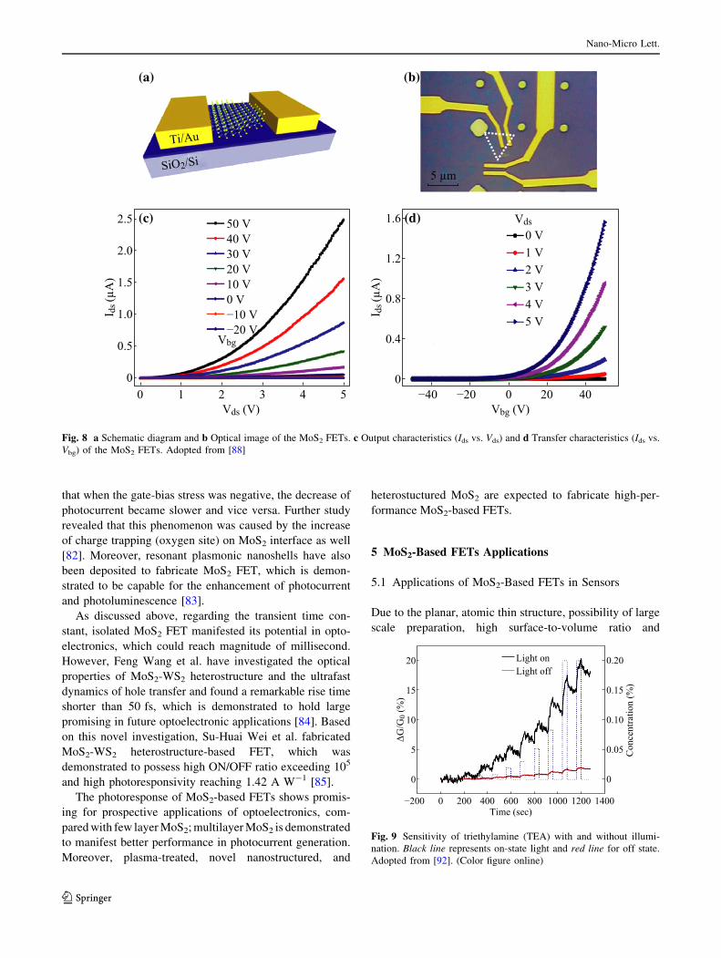
For gas sensor, Liu et al. [88] have focused on the
Schottky-contacted CVD grown monolayer MoS2 FET.
They fabricated the MoS2 FETs with 5 nm Ti/50 nm Au
metal contact; the schematic diagram and optical image of
MoS2 FETs are shown in Fig. 8a, b, respectively. Figure 8c
exhibits the Ids versus Vds output characteristics of as-fab-
ricated FET, and transfer characteristics (Ids vs. Vbg) is il-
lustrated in Fig. 8d, manifesting the n-type characteristic,
which corresponds to the n-type electronic property of
MoS2 semiconductor [89]. Note that, there exists a
Schottky barrier (SB) in as-fabricated MoS2 FET-based
sensor (Fig. 8c). Later, they investigated the sensitivity and
the mechanism of as-fabricated FET for detecting two
poisonous gases: NO2 and NH3. Generally, conductance
(resistance) change is measured to reflect performance of
sensing and total resistance of as-fabricated FET is ex-
pressed as follows:
R ¼ Rchannel þ Rcontact ð1Þ
In this equation, Rchannel is only related to carrier concen-
tration, but Rcontact is related to both carrier concentration and
the Schottky barrier height. The relationship is exponential,
thus indicating that the Schottky barrier is a key factor in
sensitivity. With a conductance change larger than 20 and
40 %, the sensitivity of this MoS2 FET-based chemical sensor
can reach 20 parts per billion (ppb) for NO2 and 1 parts per
million (ppm) for NH3, respectively. This detection limit is the
lowest gas concentration detected compared with the other
experiments: Li et al. [90] used multilayer MoS2 film FET to
detect NO (detection limit *800 ppb) and Late et al. [91]
presented a detection limit of several hundred ppm for both
NH3 and NO2 using atomically thin-layered MoS2 transistors.
Moreover, Liu et al. found part of MoS2 devices exhibiting
more Ohmic contact, but the little conductance change
(\5 %) upon exposure to NO2 at concentrations up to 400 ppb
further manifests that Schottky barrier modulation plays a
more important role in these MoS2 FET-based sensors. That
is, it is realizable to modulate the Schottky barrier contact of
MoS2-based FET sensor and achieve higher performance at
the sub-ppb level.
Moreover, in monolayer MoS2-based FET sensor, sen-
sitivity of detecting triethylamine (TEA) can be enhanced
by illumination [92] as illustrated in Fig. 9. DG stands for
the decrease of initial conductance (G0) of FET when ex-
posed to TEA, the calculated DG/G0 is the sensitivity. The
black line represents that the light is on and red line for off
state, showing the increase of sensitivity with longer time
(about 1 order of magnitude), which may attributes to the
enhancement of conductivity under illumination. Conve-
nient way of fabricating MoS2-based FET sensor is ex-
pected, which is significant in practical applications [25].
In addition, Lee et al. fabricated the sensor without di-
electric layer on multilayer MoS2 FETs, which possess
hydrophobic interface that serves as novel non-dielectric
layer, thus resulting in the improvement of sensitivity [93].
With the nature of 2D structure, MoS2-based FET sensors
should be studied further to explore higher sensitivity,
lower cost, more effective biosensors, and chemical gas
sensors, which are potential for next-generation medical
diagnosis of cancer, environment monitoring, and food
safety.
5.2 Applications of MoS2-Based FETs in Memory
Devices
Multibit memory devices have attracted much attention and
investigations, which are generally fabricated by organic
semiconductor materials [94], nanostructure materials [95],
and phase-change materials [96]. It is significant to explore
a novel convenient method to fabricate multibit memory.
Toward this effort, Chen et al. [97] have explored an ap-
proach to fabricated MoS2 FET-based 2–4 bit memory
devices. They proposed a plasma-treated way and found
that this plasma-treated MoS2 FET could act as multibit
memory devices as illustrated in Fig. 10. Figure 10a is the
schematic diagram of plasma-treated MoS2 FET, of which
a 15–30-nm MoS2 film served as the active layer with 5 nm
Ti/50 nm Au electrode. The optical image of as-treated
MoS2 FET is shown in Fig. 10b. Herein, D and S are the Ti
electrode and Au electrode, respectively. Figure 10c shows
the transport characteristic curve (IDS (Ids) vs. VG); in ad-
dition, the measurements of retention are given in Fig. 10d,
and it can be seen that the write/read ratio is about 103 after
1 h and 400 after 3 days. Accordingly, a write/read ratio
value of about 64 of the as-fabricated FET aged after
10 years can be inferred, which is still valid for circuit
application. It is further found that the plasma-treated
MoS2 FET is faster in programing than the untreated one in
their experiments. A physical model for explaining the
performance enhancement was proposed as following: The
plasma-treated channel top layer could be separated and
forms an ambipolar charge-trapping layer, allowing the
high-performance non-volatile retention and multibit states
Nano-Micro Lett.
123

in this FET. This method is certainly worth considering for
fabrication of nanodevices since it is technically conve-
nient and provides a relatively simple way for realizing
non-volatile memory devices, which also offers an effec-
tive method to scale down current circuit in future
nanoelectronics.
Moreover, MoS2 nanoflakes have been employed as
charge-trapping layer (nano-floating gate) to fabricate or-
ganic nano-floating gate memories (NFGMs) by Kang et al.
[98], which are based on organic (poly (3-hexylthiophene)
(P3HT)) FET. The inserted solution process is convenient
and realized at low temperature to introduce MoS2 nano-
flakes between two dielectric layers: polystyrene (PS) and
poly (methyl methacrylate) (PMMA). The as-fabricated
memory device exhibits multilevel non-volatile memory
nature, as illustrated in Fig. 11. Figure 11a depicts the
endurance of this NFGM, which is more than 102 times
(under the condition of Vd = -5 V and Vg = 0 V). Pro-
graming process and corresponding voltages are shown in
Fig. 11b, and the four voltage steps are from -80 to 80 V
(-80, ?30, ?50, ?80 V). Figure 11c, d illustrates the
retention characteristics by measuring four current levels
(Abs (Id) represents the absolute value of drain current) at
Vd = -5 V and Vg = 0 V with 60 s delay, indicating the
stable retention times after 10 years. This MoS2-based
organic FET is a 2-bit memory device controlled by V and
potential for inexpensive memory devices.
6 Conclusions
In this paper, we have reviewed state-of-the-art approaches
in MoS2 FETs, such as progresses on manufacturing of
MoS2 FETs, MoS2 FET-based memory devices, and MoS2
FET-based sensors. To understanding the contact physics
based on Schottky barrier, different species of metals uti-
lized to achieve high-performance n-type and p-type MoS2
FETs are reviewed, and optimization of ferromagnetic
contact for spintronics applications are discussed too. In-
trinsic properties measured by four-terminal measurements
are highlighted, which is an effective method to estimate
contact quality of MoS2-based FETs. In addition, gate di-
electric formation and doping strategies are studied and
provide guidelines for prospective manufacturing of MoS2-
based FETs.
Low-frequency noise (LFN) analysis was carried out for
studying the performance of MoS2 FETs. FETs made of
bilayer MoS2 present a longer trap decay time. Further
analysis shows that the LFN subjects not only to the phy-
sical properties of the channels but also the behavior of
10 year storageWR/ER ratio ~64
3 days storageWR/ER ratio ~400
Write
Erase
−100 V
+100 V
VDS=0.01 V
VG (V)
O2 plasma-treated FETVDS=0.1 V
Time (sec)
I DS
(A)
I DS
(A)
10−3−100 −50 0 50 100 10−1210−11
10−10
10−9
10−8
10−7
10−6
10−11
10−10
10−9
10−8
10−7
10−1 101 103 105 107 109
Gate
Plasma-TreatedMoS2 layers
Plasma-Treated MoS2 FET channelPlasma treatment(a) (b)
(c) (d)
WriteErase
SiO2
IDS
p+-Si
Source
Drain
2 μm
SD
Fig. 10 a The schematic diagram of plasma-treated MoS2 FET. b The optical image of as-treated MoS2 FET. c Transfer characteristic curve (Ids
vs. VG). d Retention measurements of this FET. Adopted from [97]
Nano-Micro Lett.
123

contacts in MoS2 FETs. The noise increase in aged MoS2
FETs is caused by aging of the MoS2 channels rather than
the aging of contacts. This phenomenon is significant in
MoS2 as well as in other 2D materials FETs for the opti-
mization of channel implementation.
Photoresponse of MoS2-based FETs are critical and
considered in this review, mainly focusing on the pho-
tocurrent generation with and without illumination. More-
over, MoS2-based FETs are utilized in gas and biological
sensors, showing its high sensitivity and selectivity. MoS2
nanoflakes are fabricated and successfully employed in
organic nano-floating gate memories (NFGMs) as non-
volatile random-access memory (NVRAM), providing an
instance for nanomaterials used in memory devices. The
plasma-treated MoS2 FETs can serve as multibit memory
devices and exhibit excellent storage capacities, suggesting
the significance of plasma in performance improving of
MoS2 electronic devices.
To conclude, MoS2 FETs based on thin-film and nano-
size structures are investigated. Some key optical and
electronic properties of these MoS2 FET devices are unique
and superior than FETs made of conventional semicon-
ductors, thus are suitable for novel electronic and opto-
electronic applications.
Open Access This article is distributed under the terms of the
Creative Commons Attribution License which permits any use, dis-
tribution, and reproduction in any medium, provided the original
author(s) and the source are credited.
References
1. D. Jariwala, V.K. Sangwan, L.J. Lauhon, T.J. Marks, M.C.
Hersam, Emerging device applications for semiconducting two-
dimensional transition metal dichalcogenides. ACS Nano 8(2),
1102–1120 (2014). doi:10.1021/nn500064s
2. Q.H. Wang, K. Kalantar-Zadeh, A. Kis, J.N. Coleman, M.S.
Strano, Electronics and optoelectronics of two-dimensional
transition metal dichalcogenides. Nat. Nanotechnol. 7(11),
699–712 (2012). doi:10.1038/nnano.2012.193
3. G. Plechinger, J. Mann, E. Preciado, D. Barroso, A. Nguyen, J.
Eroms, C. Schueller, L. Bartels, T. Korn, A direct comparison of
CVD-grown and exfoliated MoS2 using optical spectroscopy.
Semicond. Sci Tech. 29(6), 064008 (2014). doi:10.1088/0268-
1242/29/6/064008
at Vd=−5 V, Vg=0 V
at Vd=−5 V, Vg=0 V
at Vd=0 V
Readingat Vd=−5 V
Erasing−80 V
30 V50 V
Programming
80 V
0 V
10−6
10−6
10−7
10−8
10−9
10−10
10−11
10−7
10−8
10−9
10−6
10−7
10−8
10−9
10−10
10−111×1040
Time (sec) Time (sec)2×10⁴ 3×10⁴ 4×10⁴ 103 105
10 yr
107 109
Abs
(Id,
A)
Abs
(Id,
A)
Abs
(Id,
A)
0 20
(a) (b)
(c) (d)
40 60 80 100 120Endurance cycles
140
“3”
“2”
“1”
“0”
“3”“3”
“2”
“1”
“0”
“2”
“1”
“0”
Vg (
V)
Fig. 11 a Endurance measurement of as-fabricated NFGM under the condition of Vd = -5 V and Vg = 0 V. b Programming process and
corresponding voltages are shown, four voltage steps are -80, ?30, ?50, and ?80 V. c and d illustrate the retention characteristics of four
current levels at Vd = -5 V and Vg = 0 V with 60 s delay. Adopted from [98]
Nano-Micro Lett.
123

4. E.S. Kadantsev, P. Hawrylak, Electronic structure of a single
MoS2 monolayer. Solid State Commun. 152(10), 909–913
(2012). doi:10.1016/j.ssc.2012.02.005
5. A. Kumar, P.K. Ahluwalia, A first principle comparative study of
electronic and optical properties of 1H-MoS2 and 2H-MoS2.
Mater. Chem. Phys. 135(2–3), 755–761 (2012). doi:10.1016/j.
matchemphys.2012.05.055
6. Q. Zhang, Y. Cheng, L.Y. Gan, U. Schwingenschloegl, Giant
valley drifts in uniaxially strained monolayer MoS2. Phys. Rev. B
88(24), 245447 (2013). doi:10.1103/PhysRevB.88.245447
7. B. Chakraborty, H.S.S.R. Matte, A.K. Sood, C.N.R. Rao, Layer-
dependent resonant Raman scattering of a few layer MoS2.
J. Raman Spectrosc. 44(1), 92–96 (2013). doi:10.1002/jrs.4147
8. Z.M. Wang, MoS2: Materials, Physics, and Devices (Springer,
Ney work, 21, pp:1–291, 2014)
9. R. Frindt, Single crystals of MoS2 several molecular layers thick.
J. Appl. Phys. 37(4), 1928–1929 (1966). doi:10.1063/1.1708627
10. Y.H. Lee, X.Q. Zhang, W. Zhang, M.T. Chang, C.T. Lin, K.D.
Chang, Y.C. Yu, J.T.W. Wang, C.S. Chang, L.J. Li, T.W. Lin,
Synthesis of large-area MoS2 atomic layers with chemical vapor
deposition. Adv. Mater. 24(17), 2320–2325 (2012). doi:10.1002/
adma.201104798
11. H. Pan, Y.W. Zhang, Tuning the electronic and magnetic prop-
erties of MoS2 nanoribbons by strain engineering. J. Phys. Chem.
C 116(21), 11752–11757 (2012). doi:10.1021/jp3015782
12. Z. Zhou, Y. Lin, P. Zhang, E. Ashalley, M. Shafa, H. Li, J. Wu, Z.
Wang, Hydrothermal fabrication of porous MoS2 and its visible
light photocatalytic properties. Mater. Lett. 131, 122–124 (2014).
doi:10.1016/j.matlet.2014.05.162
13. R. van Leeuwen, A. Castellanos-Gomez, G.A. Steele, H.S.J. van
der Zant, W.J. Venstra, Time-domain response of atomically thin
MoS2 nanomechanical resonators. Appl. Phys. Lett. 105(4),
041911 (2014). doi:10.1063/1.4892072
14. Z. Yin, H. Li, H. Li, L. Jiang, Y. Shi, Y. Sun, G. Lu, Q. Zhang, X.
Chen, H. Zhang, Single-layer MoS2 phototransistors. ACS Nano
6(1), 74–80 (2012). doi:10.1021/nn2024557
15. F.K. Perkins, A.L. Friedman, E. Cobas, P.M. Campbell, G.G.
Jernigan, B.T. Jonker, Chemical vapor sensing with monolayer
MoS2. Nano Lett. 13(2), 668–673 (2013). doi:10.1021/nl3043079
16. O. Lopez-Sanchez, D. Lembke, M. Kayci, A. Radenovic, A. Kis,
Ultrasensitive photodetectors based on monolayer MoS2. Nat.
Nanotechnol. 8(7), 497–501 (2013). doi:10.1038/nnano.2013.100
17. B. Radisavljevic, M.B. Whitwick, A. Kis, Small-signal amplifier
based on single-layer MoS2. Appl. Phys. Lett. 101(4), 043103
(2012). doi:10.1063/1.4738986
18. S. Ding, D. Zhang, J.S. Chen, X.W. Lou, Facile synthesis of
hierarchical MoS2 microspheres composed of few-layered
nanosheets and their lithium storage properties. Nanoscale 4(1),
95–98 (2012). doi:10.1039/c1nr11552a
19. K. Chang, W. Chen, L-cysteine-assisted synthesis of layered
MoS2/graphene composites with excellent electrochemical per-
formances for lithium ion batteries. ACS Nano 5(6), 4720–4728
(2011). doi:10.1021/nn200659w
20. K.F. Mak, K. He, J. Shan, T.F. Heinz, Control of valley polar-
ization in monolayer MoS2 by optical helicity. Nat. Nanotechnol.
7(8), 494–498 (2012). doi:10.1038/nnano.2012.96
21. H. Zeng, J. Dai, W. Yao, D. Xiao, X. Cui, Valley polarization in
MoS2 monolayers by optical pumping. Nat. Nanotechnol. 7(8),
490–493 (2012). doi:10.1038/nnano.2012.95
22. X. Huang, Z. Yin, S. Wu, X. Qi, Q. He, Q. Zhang, Q. Yan, F.
Boey, H. Zhang, Graphene-based materials: synthesis, charac-
terization, properties, and applications. Small 7(14), 1876–1902
(2011). doi:10.1002/smll.201002009
23. H.S. Lee, S.W. Min, Y.G. Chang, M.K. Park, T. Nam, H. Kim,
J.H. Kim, S. Ryu, S. Im, MoS2 nanosheet phototransistors with
thickness-modulated optical energy gap. Nano Lett. 12(7),
3695–3700 (2012). doi:10.1021/nl301485q
24. H. Liu, J.J. Gu, P.D. Ye, MoS2 nanoribbon transistors: transition
from depletion mode to enhancement mode by channel-width
trimming. IEEE Electr. Device L 33(9), 1273–1275 (2012).
doi:10.1109/LED.2012.2202630
25. X. Wang, S. Yang, Q. Yue, F. Wu, J. Li, Response of MoS2
nanosheet field effect transistor under different gas environments
and its long wavelength photoresponse characteristics. J. Alloy.
Compd. 615, 989–993 (2014). doi:10.1016/j.jallcom.2014.07.016
26. G. Eda, H. Yamaguchi, D. Voiry, T. Fujita, M. Chen, M. Ch-
howalla, Photoluminescence from chemically exfoliated MoS2.
Nano Lett. 11(12), 5111–5116 (2011). doi:10.1021/nl201874w
27. B. Radisavljevic, A. Radenovic, J. Brivio, V. Giacometti, A. Kis,
Single-layer MoS2 transistors. Nat. Nanotechnol. 6(3), 147–150
(2011). doi:10.1038/nnano.2010.279
28. Y. Yoon, K. Ganapathi, S. Salahuddin, How good can monolayer
MoS2 transistors Be? Nano Lett. 11(9), 3768–3773 (2011).
doi:10.1021/nl2018178
29. F. Leonard, A.A. Talin, Electrical contacts to one- and two-di-
mensional nanomaterials. Nat. Nanotechnol. 6(12), 773–783
(2011). doi:10.1038/nnano.2011.196
30. Y. Du, L. Yang, H. Liu, P.D. Ye, Contact research strategy for
emerging molybdenum disulfide and other two-dimensional field-
effect transistors. Appl. Mater. 2(9), 092510 (2014). doi:10.1063/
1.4894198
31. H. Liu, A.T. Neal, P.D. Ye, Channel length scaling of MoS2 MOS-
FETs. ACS Nano 6(10), 8563–8569 (2012). doi:10.1021/nn303513c
32. S. Das, H.Y. Chen, A.V. Penumatcha, J. Appenzeller, High
performance multilayer MoS2 transistors with scandium contacts.
Nano Lett. 13(1), 100–105 (2013). doi:10.1021/nl303583v
33. J.H. Kang, D. Sarkar, W. Liu, D. Jena, K. Banerjee, A compu-
tational study of metal-contacts to beyond-graphene 2D semi-
conductor materials. 2012 IEEE Int. Electr. Devices Meet.
(IEDM) (2012). doi:10.1109/IEDM.2012.6479060
34. W. Liu, J.H. Kang, W. Cao, D. Sarkar, Y. Khatami, D. Jena, K.
Banerjee, High-performance few-layer-MoS2 field-effect-tran-
sistor with record low contact-resistance, 2013 IEEE Int. Electr.
Devices Meet. (IEDM) (2013). doi:10.1109/IEDM.2013.6724660
35. J. Kang, W. Liu, K. Banerjee, High-performance MoS2 transistors
with low-resistance molybdenum contacts. Appl. Phys. Lett.
104(9), 093106 (2014). doi:10.1063/1.4866340
36. S. Kim, A. Konar, W.S. Hwang, J.H. Lee, J. Lee, J. Yang, C.
Jung, H. Kim, J.B. Yoo, J.Y. Choi, Y.W. Jin, S.Y. Lee, D. Jena,
W. Choi, K. Kim, High-mobility and low-power thin-film tran-
sistors based on multilayer MoS2 crystals. Nat. Commun. 3, 1011
(2012). doi:10.1038/ncomms2018
37. M. Fontana, T. Deppe, A.K. Boyd, M. Rinzan, A.Y. Liu, M.
Paranjape, P. Barbara, Electron-hole transport and photovoltaic
effect in gated MoS2 Schottky junctions. Sci. Rep-UK 3, 1634
(2013). doi:10.1038/srep01634
38. S. Chuang, C. Battaglia, A. Azcatl, S. McDonnell, J.S. Kang, X.
Yin, M. Tosun, R. Kapadia, H. Fang, R.M. Wallace, A. Javey,
MoS2 P-type transistors and diodes enabled by high work func-
tion moox contacts. Nano Lett. 14(3), 1337–1342 (2014). doi:10.
1021/nl4043505
39. C. Battaglia, X. Yin, M. Zheng, I.D. Sharp, T. Chen, S.
McDonnell, A. Azcatl, C. Carraro, B. Ma, R. Maboudian, R.M.
Wallace, A. Javey, Hole selective MoOx contact for silicon solar
cells. Nano Lett. 14(2), 967–971 (2014). doi:10.1021/nl404389u
40. I. Popov, G. Seifert, D. Tomanek, Designing electrical contacts to
MoS2 monolayers: a computational study. Phy. Rev. Lett.
108(15), 156802 (2012). doi:10.1103/PhysRevLett.108.156802
41. J.-R. Chen, P.M. Odenthal, A.G. Swartz, G.C. Floyd, H. Wen,
K.Y. Luo, R.K. Kawakami, Control of schottky barriers in single
Nano-Micro Lett.
123

layer MoS2 transistors with ferromagnetic contacts. Nano Lett.
13(7), 3106–3110 (2013). doi:10.1021/nl4010157
42. A. Dankert, L. Langouche, M.V. Kamalakar, S.P. Dash, High-
performance molybdenum disulfide field-effect transistors with
spin tunnel contacts. ACS Nano 8(1), 476–482 (2014). doi:10.
1021/nn404961e
43. N.R. Pradhan, D. Rhodes, Q. Zhang, S. Talapatra, M. Terrones,
P.M. Ajayan, L. Balicas, Intrinsic carrier mobility of multi-lay-
ered MoS2 field-effect transistors on SiO2. Appl. Phys. Lett.
102(12), 123105 (2013). doi:10.1063/1.4799172
44. W. Bao, X. Cai, D. Kim, K. Sridhara, M.S. Fuhrer, High mobility
ambipolar MoS2 field-effect transistors: substrate and dielectric
effects. Appl. Phys. Lett. 102(4), 042104 (2013). doi:10.1063/1.
4789365
45. B.W.H. Baugher, H.O.H. Churchill, Y. Yang, P. Jarillo-Herrero,
Intrinsic electronic transport properties of high-quality monolayer
and bilayer MoS2. Nano Lett. 13(9), 4212–4216 (2013). doi:10.
1021/nl401916s
46. N.R. Pradhan, D. Rhodes, Y. Xin, S. Memaran, L. Bhaskaran, M.
Siddiq, S. Hill, P.M. Ajayan, L. Balicas, Ambipolar molybdenum
diselenide field-effect transistors: field-effect and hall mobilities.
ACS Nano 8(8), 7923–7929 (2014). doi:10.1021/nn501693d
47. J. Yoon, W. Park, G.Y. Bae, Y. Kim, H.S. Jang, Y. Hyun, S.K.
Lim, Y.H. Kahng, W.K. Hong, B.H. Lee, H.C. Ko, Highly flex-
ible and transparent multilayer MoS2 transistors with graphene
electrodes. Small 9(19), 3295–3300 (2013). doi:10.1002/smll.
201300134
48. R. Kappera, D. Voiry, S.E. Yalcin, B. Branch, G. Gupta, A.D.
Mohite, M. Chhowalla, Phase-engineered low-resistance contacts
for ultrathin MoS2 transistors. Nat. Mater. 13(12), 1128–1134
(2014). doi:10.1038/nmat4080
49. M. Amani, M.L. Chin, A.G. Birdwell, T.P. O’Regan, S. Najmaei,
Z. Liu, P.M. Ajayan, J. Lou, M. Dubey, Electrical performance of
monolayer MoS2 field-effect transistors prepared by chemical
vapor deposition. Appl. Phys. Lett. 102(19), 193107 (2013).
doi:10.1063/1.4804546
50. H. Wang, L. Yu, Y.H. Lee, Y. Shi, A. Hsu, M.L. Chin, L.-J. Li,
M. Dubey, J. Kong, T. Palacios, Integrated circuits based on
bilayer MoS2 transistors. Nano Lett. 12(9), 4674–4680 (2012).
doi:10.1021/nl302015v
51. L. Zeng, Z. Xin, S. Chen, G. Du, J. Kang, X. Liu, Remote phonon
and impurity screening effect of substrate and gate dielectric on
electron dynamics in single layer MoS2. Appl. Phys. Lett.
103(11), 113505 (2013). doi:10.1063/1.4821344
52. D. Jena, A. Konar, Enhancement of carrier mobility in semi-
conductor nanostructures by dielectric engineering. Phys. Rev.
Lett. 98(13), 136805 (2007). doi:10.1103/PhysRevLett.98.
136805
53. H. Liu, K. Xu, X. Zhang, P.D. Ye, The integration of high-k di-
electric on two-dimensional crystals by atomic layer deposition.
Appl. Phys. Lett. 100(15), 152115 (2012). doi:10.1063/1.3703595
54. J. Swerts, N. Peys, L. Nyns, A. Delabie, A. Franquet, J.W. Maes,
S. Van Elshocht, S. De Gendt, Impact of precursor chemistry and
process conditions on the scalability of ALD HfO2 gate di-
electrics. J. Electrochem. Soc. 157(1), G26–G31 (2010). doi:10.
1149/1.3258664
55. J. Yang, S. Kim, W. Choi, S.H. Park, Y. Jung, M.H. Cho, H. Kim,
Improved growth behavior of atomic-layer-deposited high-k di-
electrics on multilayer MoS2 by oxygen plasma pretreatment.
ACS Appl. Mater. Inter. 5(11), 4739–4744 (2013). doi:10.1021/
am303261c
56. A. Azcatl, S. McDonnell, K.C. Santosh, X. Peng, H. Dong, X.
Qin, R. Addou, G.I. Mordi, N. Lu, J. Kim, M.J. Kim, K. Cho,
R.M. Wallace, MoS2 functionalization for ultra-thin atomic layer
deposited dielectrics. Appl. Phys. Lett. 104(11), 111601 (2014).
doi:10.1063/1.4869149
57. L. Cheng, X. Qin, A.T. Lucero, A. Azcatl, J. Huang, R.M.
Wallace, K. Cho, J. Kim, Atomic layer deposition of a high-
k dielectric on MoS2 using trimethylaluminum and ozone. ACS
Appl. Mater. Inter. 6(15), 11834–11838 (2014). doi:10.1021/
am5032105
58. Y. Du, H. Liu, A.T. Neal, M. Si, P.D. Ye, Molecular doping of
multilayer MoS2 field-effect transistors: reduction in sheet and
contact resistances. IEEE Electr. Device L 34(10), 1328–1330
(2013). doi:10.1109/LED.2013.2277311
59. J.D. Lin, C. Han, F. Wang, R. Wang, D. Xiang, S. Qin, X.A.
Zhang, L. Wang, H. Zhang, A.T.S. Wee, W. Chen, Electron-
doping-enhanced trion formation in monolayer molybdenum
disulfide functionalized with cesium carbonate. ACS Nano 8(5),
5323–5329 (2014). doi:10.1021/nn501580c
60. H. Fang, M. Tosun, G. Seol, T.C. Chang, K. Takei, J. Guo, A.
Javey, Degenerate n-doping of few-layer transition metal
dichalcogenides by potassium. Nano Lett. 13(5), 1991–1995
(2013). doi:10.1021/nl400044m
61. D. Kiriya, M. Tosun, P. Zhao, J.S. Kang, A. Javey, Air-stable
surface charge transfer doping of MoS2 by benzyl viologen.
JACS 136(22), 7853–7856 (2014). doi:10.1021/ja5033327
62. L. Yang, K. Majumdar, H. Liu, Y. Du, H. Wu, M. Hatzistergos,
P.Y. Hung, R. Tieckelmann, W. Tsai, C. Hobbs, P.D. Ye,
Chloride molecular doping technique on 2D materials: WS2 and
MoS2. Nano Lett. 14(11), 6275–6280 (2014). doi:10.1021/
nl502603d
63. Y. Wu, Y. Lin, A.A. Bol, K.A. Jenkins, F. Xia, D.B. Farmer, Y.
Zhu, P. Avouris, High-frequency, scaled graphene transistors on
diamond-like carbon. Nature 472(7341), 74–78 (2011). doi:10.
1038/nature09979
64. J.B. Johnson, The Schottky effect in low frequency circuits. Phys.
Rev. 26(1), 71 (1925). doi:10.1103/PhysRev.26.71
65. B.H. Calhoun, A. Wang, A. Chandrakasan, Device sizing for
minimum energy operation in subthreshold circuits. (pp: 95–98,
3–6 Oct. 2004). doi:10.1109/CICC.2004.1358745
66. J.M. Chang, A.A. Abidi, C.R. Viswanathan, Flicker noise in
CMOS transistors from subthreshold to strong inversion at var-
ious temperatures. IEEE Trans. Electron Devices 41(11),
1965–1971 (1994). doi:10.1109/16.333812
67. S. Ghatak, A.N. Pal, A. Ghosh, Nature of electronic states in
atomically thin MoS2 field-effect transistors. ACS Nano 5(10),
7707–7712 (2011). doi:10.1021/nn202852j
68. B. Radisavljevic, M.B. Whitwick, A. Kis, Integrated circuits and
logic operations based on single-layer MoS2. ACS Nano 5(12),
9934–9938 (2011). doi:10.1021/nn203715c
69. C. Kayis, J.H. Leach, C.Y. Zhu, M. Wu, X. Li, U. Oezguer, H.
Morkoc, X. Yang, V. Misra, P.H. Handel, Low-frequency noise
measurements of AlGaN/GaN metal-oxide-semiconductor
heterostructure field-effect transistors with HfAlO gate dielectric.
IEEE Electr. Device L. 31(9), 1041–1043 (2010). doi:10.1109/
LED.2010.2055823
70. A.A. Balandin, Noise and Fluctuations Control in Electronic
Devices (American Scientific Publishers, Los Angeles, pp.1–411,
2002)
71. E. Simoen, A. Mercha, C. Claeys, E. Young, Correlation between
the 1/f noise parameters and the effective low-field mobility in
HfO2 gate dielectric n-channel metal-oxide-semiconductor field-
effect transistors. Appl. Phys. Lett. 85(6), 1057–1059 (2004).
doi:10.1063/1.1779967
72. X. Xie, D. Sarkar, W. Liu, J. Kang, O. Marinov, M.J. Deen, K.
Banerjee, Low-frequency noise in bilayer MoS2 transistor. ACS
Nano 8(6), 5633–5640 (2014). doi:10.1021/nn4066473
73. V.K. Sangwan, H.N. Arnold, D. Jariwala, T.J. Marks, L.J. Lau-
hon, M.C. Hersam, Low-frequency electronic noise in single-
layer MoS2 transistors. Nano Lett. 13(9), 4351–4355 (2013).
doi:10.1021/nl402150r
Nano-Micro Lett.
123

74. H.-J. Kwon, H. Kang, J. Jang, S. Kim, C.P. Grigoropoulos,
Analysis of flicker noise in two-dimensional multilayer MoS2
transistors. Appl. Phys. Lett. 104(8), 083110 (2014). doi:10.1063/
1.4866785
75. J. Renteria, R. Samnakay, S.L. Rumyantsev, C. Jiang, P. Goli,
M.S. Shur, A.A. Balandin, Low-frequency 1/f noise in MoS2
transistors: relative contributions of the channel and contacts.
Appl. Phys. Lett. 104(15), 153104 (2014). doi:10.1063/1.4871374
76. S. Ghatak, S. Mukherjee, M. Jain, D.D. Sarma, A. Ghosh, Mi-
croscopic origin of low frequency noise in MoS2 field-effect
transistors. Appl. Mater. 2(9), 092515 (2014). doi:10.1063/1.
4895955
77. A.M. Jones, H. Yu, N.J. Ghimire, S. Wu, G. Aivazian, J.S. Ross,
B. Zhao, J. Yan, D.G. Mandrus, D. Xiao, W. Yao, X. Xu, Optical
generation of excitonic valley coherence in monolayer WSe2.
Nat. Nanotechnol. 8(9), 634–638 (2013). doi:10.1038/nnano.
2013.151
78. N.R. Pradhan, S. Memaran, D.R.Z. Lu, J. Ludwig, Q. Zhou, P.
Ajayan, D. Smirnov, L. Balicas, Pronounced photovoltaic re-
sponse from PN-junctions of multi-layered MoSe2 on h-BN.
arXiv:1411.2086 (2014)
79. H.M. Li, D.Y. Lee, M.S. Choi, D. Qu, X. Liu, C.H. Ra, W.J. Yoo,
Metal-semiconductor barrier modulation for high photoresponse
in transition metal dichalcogenide field effect transistors. SCI
Rep-UK 4, 4041 (2014). doi:10.1038/srep04041
80. M.F. Khan, M.W. Iqbal, M.Z. Iqbal, M.A. Shehzad, Y. Seo, J.
Eom, Photocurrent response of MoS2 field-effect transistor by
deep ultraviolet light in atmospheric and N2 gas environments.
ACS Appl. Mater. Interface 6(23), 21645–21651 (2014). doi:10.
1021/am506716a
81. K. Cho, T.Y. Kim, W. Park, J. Park, D. Kim, J. Jang, H. Jeong, S.
Hong, T. Lee, Gate-bias stress-dependent photoconductive char-
acteristics of multi-layer MoS2 field-effect transistors. Nan-
otechnology 25(15), 155201 (2014). doi:10.1088/0957-4484/25/
15/155201
82. D.S. Tsai, D.H. Lien, M.L. Tsai, S.H. Su, K.M. Chen, J.J. Ke,
Y.C. Yu, L.J. Li, J.H. He, Trilayered MoS2 metal-semiconductor-
metal photodetectors: photogain and radiation resistance. IEEE J.
Sel. Top. Quantum 20(1), 3800206 (2014). doi:10.1109/JSTQE.
2013.2268383
83. A. Sobhani, A. Lauchner, S. Najmaei, C. Ayala-Orozco, F. Wen,
J. Lou, N.J. Halas, Enhancing the photocurrent and photolumi-
nescence of single crystal monolayer MoS2 with resonant plas-
monic nanoshells. Appl. Phys. Lett. 104(3), 031112 (2014).
doi:10.1063/1.4862745
84. X. Hong, J. Kim, S.F. Shi, Y. Zhang, C. Jin, Y. Sun, S. Tongay, J.
Wu, Y. Zhang, F. Wang, Ultrafast charge transfer in atomically
thin MoS2/WS2 heterostructures. Nat. Nanotechnol. 9(9),
682–686 (2014). doi:10.1038/nnano.2014.167
85. N. Huo, J. Kang, Z. Wei, S.S. Li, J. Li, S.H. Wei, Novel and
enhanced optoelectronic performances of multilayer MoS2-WS2
heterostructure transistors. Adv. Funct. Mater. 24(44), 7025–7031
(2014). doi:10.1002/adfm.201401504
86. D. Sarkar, W. Liu, X. Xie, A.C. Anselmo, S. Mitragotri, K.
Banerjee, MoS2 field-effect transistor for next-generation label-
free biosensors. ACS Nano 8(4), 3992–4003 (2014). doi:10.1021/
nn5009148
87. L. Wang, Y. Wang, J.I. Wong, T. Palacios, J. Kong, H.Y. Yang,
Functionalized MoS2 nanosheet-based field-effect biosensor for
label-free sensitive detection of cancer marker proteins in solu-
tion. Small 10(6), 1101–1105 (2014). doi:10.1002/smll.
201302081
88. B. Liu, L. Chen, G. Liu, A.N. Abbas, M. Fathi, C. Zhou, High-
performance chemical sensing using Schottky-contacted chemi-
cal vapor deposition grown mono layer MoS2 transistors. ACS
Nano 8(5), 5304–5314 (2014). doi:10.1021/nn5015215
89. S. Najmaei, Z. Liu, W. Zhou, X. Zou, G. Shi, S. Lei, B.I.
Yakobson, J.C. Idrobo, P.M. Ajayan, J. Lou, Vapour phase
growth and grain boundary structure of molybdenum disulphide
atomic layers. Nat. Mater. 12(8), 754–759 (2013). doi:10.1038/
nmat3673
90. H. Li, Z. Yin, Q. He, H. Li, X. Huang, G. Lu, D.W.H. Fam,
A.I.Y. Tok, Q. Zhang, H. Zhang, Fabrication of single-and
multilayer MoS2 film-based field-effect transistors for sensing
NO at room temperature. Small 8(1), 63–67 (2012). doi:10.1002/
smll.201101016
91. D.J. Late, Y.K. Huang, B. Liu, J. Acharya, S.N. Shirodkar, J. Luo,
A. Yan, D. Charles, U.V. Waghmare, V.P. Dravid, C.N.R. Rao,
Sensing behavior of atomically thin-layered MoS2 transistors.
ACS Nano 7(6), 4879–4891 (2013). doi:10.1021/nn400026u
92. A.L. Friedman, F.K. Perkins, E. Cobas, G.G. Jernigan, P.M.
Campbell, A.T. Hanbicki, B.T. Jonker, Chemical vapor sensing
of two-dimensional MoS2 field effect transistor devices. Solid
State Electron. 101, 2–7 (2014). doi:10.1016/j.sse.2014.06.013
93. J. Lee, P. Dak, Y. Lee, H. Park, W. Choi, M.A. Alam, S. Kim,
Two-dimensional layered MoS2 biosensors enable highly sensi-
tive detection of biomolecules. Sci. Rep. 4, 7352 (2014). doi:10.
1038/srep07352
94. Y. Guo, C. Di, S. Ye, X. Sun, J. Zheng, Y. Wen, W. Wu, G. Yu,
Y. Liu, Multibit storage of organic thin-film field-effect transis-
tors. Adv. Mater. 21(19), 1954–1959 (2009). doi:10.1002/adma.
200802430
95. J.I. Sohn, S.S. Choi, S.M. Morris, J.S. Bendall, H.J. Coles, W.K.
Hong, G. Jo, T. Lee, M.E. Welland, Novel nonvolatile memory
with multibit storage based on a ZnO nanowire transistor. Nano
Lett. 10(11), 4316–4320 (2010). doi:10.1021/nl1013713
96. T. Nirschl, J.B. Philipp, T.D. Flapp, G.W. Burr, B. Rajendran,
M.H. Leeo, A. Schrott, M. Yang, M. Breitwisch, C.F. Chen, E.
Joseph, M. Lamorey, R. Cheek, S.H. Chen, S. Zaidi, S. Raoux,
Y.C. Chen, Y. Zhu, R. Bergmann, H.L. Lung, C. Lam, Write
strategies for 2 and 4-bit multi-level phase-change memory. IEEE
Electr. Devices Meet. (pp: 461–464, 10–12 Dec. 2007). doi:10.
1109/IEDM.2007.4418973
97. M. Chen, H. Nam, S. Wi, G. Priessnitz, I.M. Gunawan, X. Liang,
Multibit data storage states formed in plasma-treated MoS2
transistors. ACS Nano 8(4), 4023–4032 (2014). doi:10.1021/
nn501181t
98. M. Kang, Y.A. Kim, J.M. Yun, D. Khim, J. Kim, Y.Y. Noh, K.J.
Baeg, D.Y. Kim, Stable charge storing in two-dimensional MoS2
nanoflake floating gates for multilevel organic flash memory.
Nanoscale 6(21), 12315–12323 (2014). doi:10.1039/
C4NR03448A
Nano-Micro Lett.
123