Advanced technologies for transient faults …raiub/BOOK_content/Section_2/Ch21_sonza/... · Web...
34
Advanced technologies for transient faults detection and compensation Authors Matteo Sonza Reorda, Luca Sterpone, Massimo Violante, Politecnico di Torino, Dip. di Automatica e Informatica, Torino, Italy ABSTRACT Transient faults became an increasing issue in the past few years as smaller geometries of newer, highly miniaturized, silicon manufacturing technologies brought to the mass-market failure mechanisms traditionally bound to niche markets as electronic equipments for avionic, space or nuclear applications. This chapter presents the origin of transient faults, it discusses the propagation mechanism, it outlines models devised to represent them and finally it discusses the state-of-the-art design techniques that can be used to detect and correct transient faults. The concepts of hardware, data and time redundancy are presented, and their implementations to cope with transient faults affecting storage elements, combinational logic and IP-cores (e.g., processor cores) typically found in a System-on- Chip are discussed. 1. INTRODUCTION Advanced semiconductor technologies developed in the past few years are allowing giant leaps forward to the electronic industry. Nowadays, portable devices are available that provide several orders of magnitude more computing power than top-of-the-line workstations of few years ago. Advanced semiconductor technologies are able to achieve such improvements by shrinking the feature size that is now at 22 nm and below, allowing integrating millions of devices on a single chip. As a result, it is now possible to manufacture an entire system (encompassing processors, companion chips, memories and input/output modules) on a single chip. Smaller transistors are also able to switch faster, thus allowing operational frequencies in the GHz range.
Transcript of Advanced technologies for transient faults …raiub/BOOK_content/Section_2/Ch21_sonza/... · Web...

Advanced technologies for transient faults detection and compensation
AuthorsMatteo Sonza Reorda, Luca Sterpone, Massimo Violante, Politecnico di Torino, Dip. di Automatica e Informatica, Torino, Italy
ABSTRACTTransient faults became an increasing issue in the past few years as smaller geometries of newer, highly miniaturized, silicon manufacturing technologies brought to the mass-market failure mechanisms traditionally bound to niche markets as electronic equipments for avionic, space or nuclear applications. This chapter presents the origin of transient faults, it discusses the propagation mechanism, it outlines models devised to represent them and finally it discusses the state-of-the-art design techniques that can be used to detect and correct transient faults. The concepts of hardware, data and time redundancy are presented, and their implementations to cope with transient faults affecting storage elements, combinational logic and IP-cores (e.g., processor cores) typically found in a System-on-Chip are discussed.
1. INTRODUCTION Advanced semiconductor technologies developed in the past few years are allowing giant leaps forward to the electronic industry. Nowadays, portable devices are available that provide several orders of magnitude more computing power than top-of-the-line workstations of few years ago.Advanced semiconductor technologies are able to achieve such improvements by shrinking the feature size that is now at 22 nm and below, allowing integrating millions of devices on a single chip. As a result, it is now possible to manufacture an entire system (encompassing processors, companion chips, memories and input/output modules) on a single chip. Smaller transistors are also able to switch faster, thus allowing operational frequencies in the GHz range. Finally, low operational voltages are possible, significantly reducing the energy needs of complex chips.All these benefits have however a downside in the higher sensitivity of newer devices to soft errors. The reduced amount of charge needed to store memory bits, the increased operational frequencies, as well as the reduced noise margins coming from lower operational voltages are making the occurrence of soft errors, i.e., unexpected random failures of the system, more probable during system lifetime.Among the different sources of soft errors, radiation induced events are becoming more and more important, and interest is growing on this topic from both the academic and the industrial communities.As described in (Dodd et al., 2004), when ionizing radiations (heavy ions or, protons in space, neutrons, and alpha particles in the earth atmosphere) hit the sensitive volume of a semiconductor device (its reserve biased depletion region) the injected charge is accelerated by an electric field, resulting in a parasitic current than can produce a number of effects, generally referred to as Single Event Effects (SEEs). Single Event Latchup (SEL) is the destructive event that takes place when the parasitic current triggers non-functional structures hidden in the semiconductor device (like parasitic transistors that shorten ground lines to power lines, which should never conduct when the device is operating correctly). Single Event Upset (SEU) is the not-destructive event that takes place when the parasitic current is able to trigger the modification of a storage cell, whose content flips from 0 to 1, or vice-versa. In case the injected charge reaches the sensitive volume of more than one memory device, multiple SEUs may happen simultaneously, giving rise to the phenomena known as Multiple Bit Upset (MBU). Finally, Single Event Transient (SET) is the not-destructive event that takes place when the parasitic current

2
produces glitches on the values of nets in the circuit compatible with the noise margins of the technology, thus result in the temporary modification of the value of the nets from 0 to 1, or vice-versa.Among SEEs, SEL is the most worrisome, as it corresponds to the destruction of the device, and hence it is normally solved by means of SEL-aware layout of silicon cells, or by current sensing and limiting circuits. SEUs, MBUs, and SETs can be tackled in different ways, depending on the market the application aims at. When vertical, high-budget, applications are considered, like for example electronic devices for telecom satellites, SEE-immune manufacturing technologies can be adopted, which are by-construction immune to SEUs, MBUs, and SETs, but whose costs are prohibitive for any other market. When budget-constrained applications are considered, from electronic devices for space exploration missions to automotive and commodity applications, SEUs, MBUs and SETs should be tackled by adopting fault detection and compensation techniques that allow developing dependable systems (i.e., where SEE effects produce negligible impacts on the application end user) on top of intrinsically not dependable technologies (i.e., which can be subject to SEUs, MBUs, and SETs), whose manufacturing costs are affordable.Different types of fault detection and compensation techniques have been developed in the past years, which are based on the well-known concepts of resource, information or time redundancy (Pradhan, 1996). In this chapter we first look at the source of soft errors, by presenting some background on radioactive environments, and then discussing how soft errors can be seen at the device level. When then present the most interesting mitigation techniques organized as a function of the component they aims at: processor, memory module, and random logic. Finally, we draw some conclusions.
2. BACKGROUND The purpose of this section is to present an overview of the radioactive environments, to introduce the reader to the physical roots of soft errors. Afterwards, SEEs resulting from the interaction of ionizing radiation with the sensitive volume of semiconductor devices are discussed at the device level, defining some fault models useful to present fault detection and compensation techniques.
2.1. Radioactive Environments The sources of radiations can be classified in different ways, depending on where the system is deployed. We can consider three so-called radiation environments: space, atmospheric, and ground radiation environments (Barth et al., 2003).The space radiation environment is composed of particles trapped by planetary magnetospheres (protons, electrons, and heavier ions), galactic cosmic ray particles (heavy ions and protons) and particles from solar events, such as coronal mass ejection and flares, which produce energetic protons, alpha particles, heavy ions, and electrons (Barth et al., 2003). The maximum energy the particles have ranges from 10 MeV for trapped electrons up to 1 TeV for galactic cosmic rays (1 eV being equivalent to 16x10 -21
Joules). Due to the very high energies involved, shielding may not be effective in protecting circuits, and therefore the impact of ionizing radiation on electronic devices should be investigated deeply, to devise effective fault compensation techniques.Atmospheric and ground radiation environments are quite different with respect to the space environment. Indeed, when cosmic ray and solar particles enter the Earth’s atmosphere, they interact with atoms of nitrogen and oxygen, and are they are attenuated. The product of the attenuation process is a shower of protons, electrons, neutrons, heavy ions, muons, and pions. Among these particles, the most important ones are neutrons, which start to appear from 330 Km of altitude. Neutron density increases up to the peak density found at about 20 Km of altitude, and then it decreases until the ground level, where the neutron density is about 1/500 of the peak one (Taber et al., 1995). The maximum energy observed for the particles in the atmospheric radiation environment is about some hundreds of MeV.

3
At the ground level, beside neutrons resulting from the interaction of galactic cosmic ray and sun particles with the atmosphere, second most important radiation source is the man-produce radiation (nuclear facilities).No matter the radiation environment where the system is deployed, we have that when radiations interact with semiconductor devices two types of interactions can be observed: atomic displacement or ionization. Atomic displacement corresponds to modifications to the structure of silicon device, which may show for example displaced atoms, and it is out of the scope of this chapter. Conversely, the latter corresponds to the deposition of energy in the semiconductor, and it is focused in this chapter.Radiations may inject charge (i.e., ionize) a semiconductor device in two different ways: direct ionization by the particle that strikes the silicon, or ionization by secondary particles created by nuclear reactions between the incident particle and the silicon. Both methods are critical, since both of them may produce malfunctions (Dodd et al., 2003).When an energetic particle passes through a semiconductor material it frees electron-hole pairs along its path, and it loses energy. When all its energy is lost, the particle rests in the semiconductor, after having travelled a path length called particle range. The energy loss per unit path length of a particle travelling in a material is known as linear energy transfer (LET), measured in MeVcm2/mg: the energy loss per unit path length (MeV/cm) divided by the material density (mg/cm3). As an example, a particle having an LET of 97 MeVcm2/mg deposits a charge of 1 pC/mm in Silicon.Heavy ions inject charges in a semiconductor device by means of the mechanism called direct ionization (Dodd et al., 2003). Protons and neutrons do not produce enough charge by direct ionization to cause single-event effects, although recent studies showed that single-event effects due to direct ionization by means of protons are possible (Barak et al., 1996) in highly scaled devices. Indirect ionization is the mechanism through which protons and neutrons produce single-event effects. Proton, or neutron, entering a semiconductor device produces atomic reactions with silicon atoms, originating by-products like alpha or gamma particles. These by-products can deposit energy along their paths by direct ionization, causing single-event effects (Dodd et al., 2003).
2.2. A device-level view of radiation effects The parasitic current induced by (direct or indirect) ionization can result in a number of different device-level effects, depending on when and where the charge injection takes place. We can broadly classify the device-level effects as destructive and not destructive. As far as digital electronic devices are considered, the most important destructive SEE is the SEL, while the most relevant not destructive SEEs are SEUs/MBUs and SETs. The following sub-sections describe these phenomena.
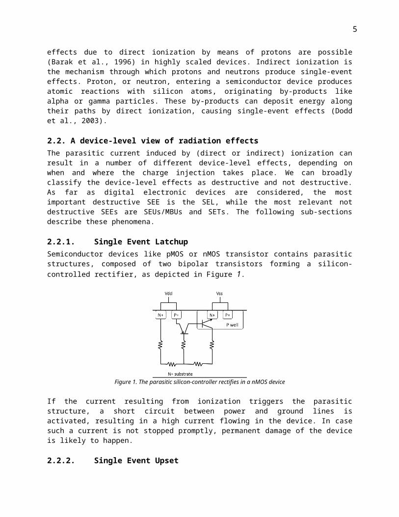
2.2.1. Single Event LatchupSemiconductor devices like pMOS or nMOS transistor contains parasitic structures, composed of two bipolar transistors forming a silicon-controlled rectifier, as depicted in Figure 1.
Figure 1. The parasitic silicon-controller rectifies in a nMOS device

4
If the current resulting from ionization triggers the parasitic structure, a short circuit between power and ground lines is activated, resulting in a high current flowing in the device. In case such a current is not stopped promptly, permanent damage of the device is likely to happen.
2.2.2. Single Event UpsetAs explained in (Dodd et al., 2003), DRAM technology refers to those devices that store bits as charge in a capacitor. In these devices no active information regeneration exists; therefore, any disturbance of the stored information provoked by ionizing radiations is persistent until it is corrected by a new write operation. Any degeneration of the stored charge that corresponds to a signal level outside the noise margin of the read circuit is sufficient to provoke an error. The noise margin is related to the memory critical charge, Qcrit, which is defined as the minimum amount of charge collected at a sensitive node that is necessary to cause the memory to change its state.The most important SEU source in DRAMs is the SEE charge collection within each capacitor used to store bits in the DRAM. These errors are caused by a single-event strike in or near either the storage capacitor or the source of the access transistor. Such a strike affects the stored charge by the collection of induced charge (Dodd et al., 2003). Such error corresponds normally to a transition of the stored bit from 1 to 0 (May et al., 1979). However, the ALPEN effects (Rajeevakumar et al., 1988) makes transitions from 0 to 1 as well. SEUs can also occur in DRAMs due to charge injection in the bit lines (Dodd et al., 2003), or a combination of charge injection close to the bit capacitor and the bit line (Rajeevakumar et al., 1988). SEUs are originated in SRAMs in according to a different phenomena with respect to DRAMs. Indeed, in SRAM the information bit in restored continuously, by means of a two inverters forming a feedback loop. When ionizing radiation injects charge into a sensitive location in a SRAM, a transient current is originated in the affected transistor. The existing feedback counterbalances the injected current, trying restoring a correct (stable) configuration. In case the current originated by the injected charge is higher than the restoring current, a voltage pulse occurs that lead to the corruption of the stored bit (Dodd et al., 2003). In case charge injection affects multiple memory cells, the resulting effect correspond to multiple SEUs happening simultaneously; such event is known as Multiple Cell Upset.
2.2.3. Single Event TransientThe progressive decreasing of the minimum dimensions of integrated circuits, accompanied by increasing operating frequencies lead on the one side the possibility of using lower supply voltages with very low noise margins but on the other side it make integrated circuits (ICs) more sensitive to Single Event Transient (SET) pulses (Baumann, 2005). In details, the shrinking technology process decreases the manufacturing sizes reducing the charge required to identify a logic state. The result is that the parasitic current provoked by the ionizing radiation is inducing a pulse effect, also called SET. The high-energy recoil and the proton-induced nuclear reactions are behind the SET generation mechanisms. In details, low-angle protons as well as heavy ions affect the silicon area close to a junction resulting in energy-loss of the signal and thus in observable SETs. The shape of SETs may be different depending on the source of the charge deposition and the conditions related to the tracks the considered high energy particle. More is the charge, more the SETs is characterized by peak heights and widths dependent from the space-charge effects (i.e. the heavy-ions generate this kind of effect).The high-injection of charge provoke a variation of the external fields internally to the considered region. The carriers within the considered region are drifted by the ambipolar diffusion reaching the edge of the plasma edge, where they drift to the external region filed thus provoking a pulse of current (i.e. The SET effect). The pulse current is drastically smaller than the normal current induced by a logic-drift. Depending on the carrier levels and on the threshold level, the penetration within the external field may change thus resulting in a different SET widths.
5
This phenomenon has been deeply investigated by experimental analysis where researchers control the radiation beam spot size, the intensity and the positions thus changing the charge injection of the particle strikes. The analysis of SET pulses has been obtained collecting datasets from pulse monitors or pulse shape analysis (PSA) that allow to generate the images of the induced SET measuring the charge and the maximum current, extracted over an area of interest. Many works investigated the nature of these events, measuring the propagation of the transient pulses through the combinational logic and routing resources in specifically designed circuits. These circuits have been demonstrated to be an effective solution for study SET effects in logic and routing resources of ICs ranging from ASICs to regular fabric such as FPGAs. In particular, for CMOS-based devices, energetic particle strikes can cause a transient voltage pulse that propagates through the circuits and may become an uncorrected data in case they are stored by a sequential element, causing disruption of the expected circuit operations. The upset rates due to SETs are dependent on the pulse width of the SET and the clock frequency of the circuit under analysis; in particular, with higher clock frequencies there are more latching clock edges to capture SET.
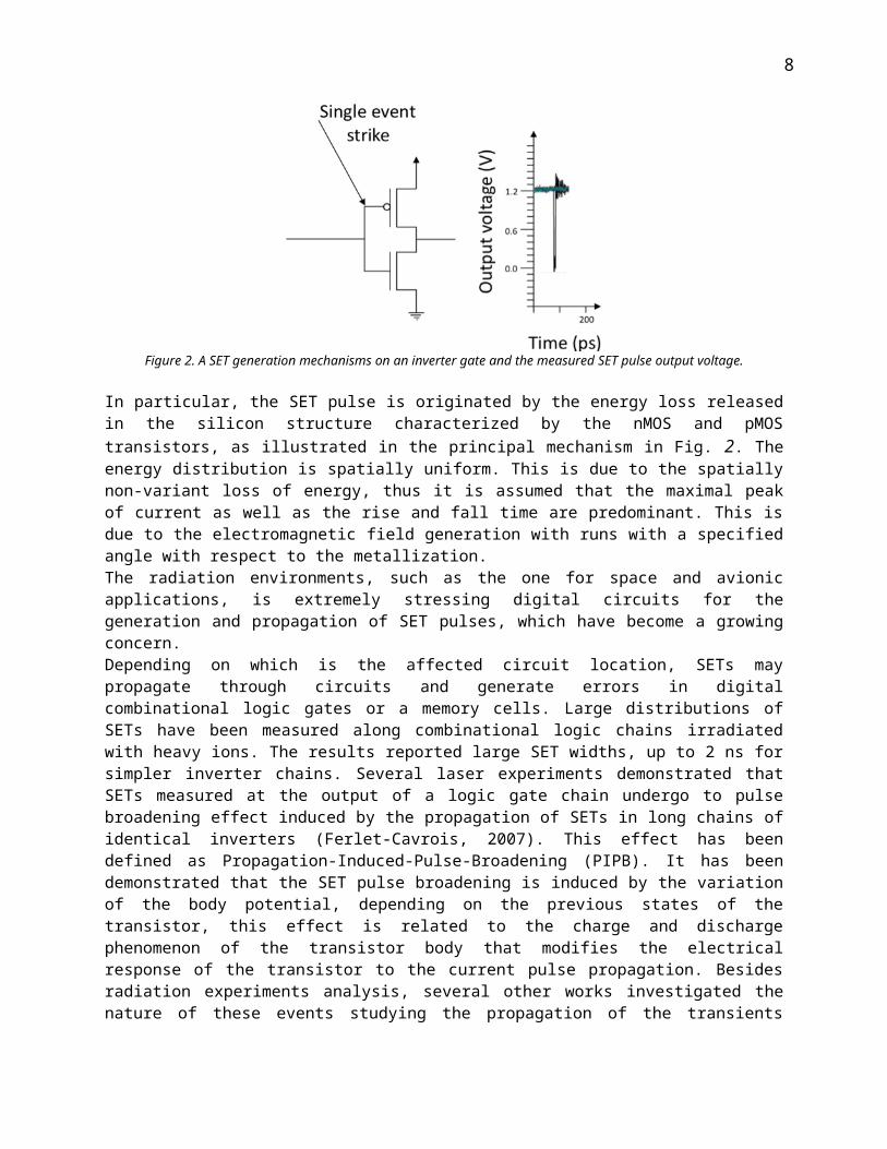
Figure 2. A SET generation mechanisms on an inverter gate and the measured SET pulse output voltage.
In particular, the SET pulse is originated by the energy loss released in the silicon structure characterized by the nMOS and pMOS transistors, as illustrated in the principal mechanism in Fig. 2. The energy distribution is spatially uniform. This is due to the spatially non-variant loss of energy, thus it is assumed that the maximal peak of current as well as the rise and fall time are predominant. This is due to the electromagnetic field generation with runs with a specified angle with respect to the metallization. The radiation environments, such as the one for space and avionic applications, is extremely stressing digital circuits for the generation and propagation of SET pulses, which have become a growing concern. Depending on which is the affected circuit location, SETs may propagate through circuits and generate errors in digital combinational logic gates or a memory cells. Large distributions of SETs have been measured along combinational logic chains irradiated with heavy ions. The results reported large SET widths, up to 2 ns for simpler inverter chains. Several laser experiments demonstrated that SETs measured at the output of a logic gate chain undergo to pulse broadening effect induced by the propagation of SETs in long chains of identical inverters (Ferlet-Cavrois, 2007). This effect has been defined as Propagation-Induced-Pulse-Broadening (PIPB). It has been demonstrated that the SET pulse broadening is induced by the variation of the body potential, depending on the previous states of the transistor, this effect is related to the charge and discharge phenomenon of the transistor body that modifies the electrical response of the transistor to the current pulse propagation. Besides radiation experiments analysis, several other works investigated the nature of these events studying the propagation of the transients through the combinational logic and routing resources of ad-hoc designed circuits. These circuits have been demonstrated to be an efficient way of studying SET effects on logic and routing

6
resources, however they are extremely far from being a representative of realistic designs. In order to study SETs effects on real designs, three kinds of analysis approaches have been adopted. First of all, radiation experiments on complex circuits and real applications provide the behavior of designs implemented in such technology under radiation. In this case, the more is the desired accuracy to study precise effects, the more it is necessary to instrument and change the circuit. Secondly, laser techniques can be used to inject pulses in a desired point of the circuit at a precise energy and controlled pulse width. On the other hand, laser testing is an extremely accurate technique that can be used once the pulse lasers are focused on the active area and the energy is adjusted at the right threshold level. The original pulse width and amplitude generated either by radiation beam or laser test are almost impossible to be directly measured, therefore the two techniques cannot be directly used to precisely characterize the SET propagation effects. Between these two techniques, electrical pulse injection can be applied to the device under analysis with known pulse signal properties (width and amplitude). In case the electrical injection is performed externally to the integrated circuit, it requires a high-performance signal generator capable to provide appropriate SET pulses (shorter than 1 ns). However, this technique requires advanced characterization of the integrated circuits pads, since the injected pulse is applied to the external pad, the pulse shape is subjected to distortion effect due to the input buffer and the internal interconnections that stem to the injection location. Thus the shape of the injected SET may be modified before reaching the desired injection point. The analysis techniques mentioned above allowed to determine that SETs pulse width and amplitude are intrinsically related to the numbers of logic gates traversed and the capacitive load of each logic gate. Researchers demonstrated that SET may be broadened or compressed depending on these parameters, and in particular the capacitive load plays an imperative role in the pulse width of the generated SET (Sterpone, 2009) (Kastensmidt Lima, 2008).
3. MITIGATION TECHNIQUESDesigners facing the problem of developing dependable systems (i.e., systems that operate without harming its users even in present on SEE-induced errors) need to adopt fault detection and compensation techniques. Indeed, as a matter of fact mainstream semiconductor technologies are prone to SEE, and radiation-hardened technologies insensitive to SEEs are too expensive for being widely adopted.
3.1. Detecting and Compensating SELSEL can be solved using two alternative approaches, one working at system level, and a second one working at layout level. The first one uses current sensors at the system level to detect the excessive current flowing when the SEL is triggered to promptly shutdown the power supply. As the device is powered off, the SEL is stopped, and after a rest period sufficient for the injected charge to annihilate, the device can be power on again. The main drawback of this approach is that the circuit state is lost at power off and therefore a suitable synchronization phase is needed when the device is power on again.The second approach uses SEL-aware design guidelines during the layout of transistors. By exploiting guard rings, the parasitic silicon controller rectifier is broken, so that SEL are likely not to take place (Troutman, 1983). To further improve such layout-based techniques, special manufacturing process can be exploited. To further reduce the SEL occurrence probability silicon grown on epitaxial layer, or silicon on insulator, is preferable over bulk silicon.
3.2. Detecting and compensating SEUs, MCUs and SETsThis section presents techniques developed for detecting and compensating not-destructive SEEs. Several approaches are presented tackling SEUs, MCUs, and SETs; for the sake of clarity, the approaches are organized as a function of the component they aim at: processor, memory or random logic.The presented approaches decline in different ways the well-known concepts of hardware, information and time redundancy (Pradhan, 1996). ), i.e., the use of more hardware, stored data or computing time

7
than actually needed for implementing the functionalities the system has to provide, to guarantee that the system operates correctly (or at least safely, i.e., without damaging the system user) even in presence of errors provoked by faulty system components
3.2.1. Processors In this section we focus only on transient faults that may affect the processor the system includes. We thus assume that memories and other chips (e.g., input/output modules) located outside the processor chip are fault free.As far as techniques for detecting and compensating transient faults in processors are considered, we can classify them in two broad categories: techniques based on processor redundancy, which achieve fault detection and compensation using more than one processor chip, and techniques based on time and/or information redundancy, which achieve fault detection and compensation using one processor chip in combination with specially crafted software.As far as techniques exploiting processor redundancy are considered we can further classify them in techniques exploiting passive redundancy, and techniques adopting active redundancy (Pradhan, 1996).
3.2.1.1. Passive redundancy The concept of passive redundancy consists in replicating the processor core three times, and in equipping the obtained processor module with a majority voter, according to the architecture depicted in Fig. 3 that is known as Triple Module Redundancy (TMR) For the sake of simplicity we showed here only the interface between the processor and the memory. In general any bus exiting the processor has to be replicated three times and voted.The three processors of the TMR architecture are synchronized and execute the same software. According to this principle, every write operation toward the memory is executed three times; therefore, under the single-fault assumption, the majority voter (which is supposed to be fault tree) is able to decide correctly the address and the value of the memory involved in every write operation.
Figure 3. Passive redundancy architecture
The most interesting property of the passive redundancy is the capability of providing a correct service even in presence on one error. Indeed, even in case one of the processor is behaving erroneously, the majority voter is able to decide the correct output that has to be sent to the memory. This property is known as fault masking, because every single fault affecting one of the processors will never have the chance to propagate to the voter output (Pradhan, 1996). Although very effective in compensating the occurrence of transient faults, the passive redundancy architecture as presented so far does not produce any mechanism to remove the fault from the faulty processor. Considering the architecture of Fig. 3, let us suppose that the tree processors are hit by a flux
8
of ionizing radiation, and that CPU 2 experiences one SEU in its program counter. Since the modification of the CPU 2 program counter, the three processors are no longer synchronized. Indeed, CPU 1 and CPU 3 continue to execute the correct program sequence, while CPU 2 executes a different one. However, the system continues to operate correctly, as the majority voter is still able to decide the correct output using the values coming from the two fault-free processors. As the flux of ionizing radiations continues to hit the processors, it is possible that a new SEU hits either CPU 1 or CPU 3. In this event, the majority voter is no longer able to decide the correct output because two processors out of three are faulty. As result, passive redundancy should be enriched with suitable techniques to remove transient faults after their detection, to guarantee that the three processors are always synchronized.The general algorithm for fault removal encompasses the following steps that perform processor synchronization:
1. Upon fault detection, the normal operations are stopped, and the three processors are forced to execute a procedure to save in memory their context (i.e., the content of the registers, program counter, and program status word). As the values are sent to the memory via the majority voter, a correct context will be stored.
2. The three processors are reset, and possibly powered off and on. As a result, all the memory elements are initialized to a correct value, removing any transient fault.
3. The correct context is copied from the memory to the three processors. At the end of this step, the three processors are synchronized, and the normal operations can be resumed.
Processor synchronization is a complex task that may be simplified by taking advantage of the peculiarity of the application where the system is employed in. For example, in case of cyclic tasks, processor synchronization can takes place at the end of each cycle by resetting the processors, and avoiding context savings.During processor synchronization, the system is unavailable to the user, as normal operations are stopped. In case outages of service are not allowed, a more complex architecture based on N Module Redundancy, with N > 3, should be used.Passive redundancy enriched with processor synchronization is currently used in a high-end processing module: the single-board computer for space, scs750, developed and commercialized by Maxwell technologies (http://www.maxwell.com/microelectronics/products/sbc/scs750.asp). The scs750 employs three PowerPC 750FX processors working synchronously, implementing the TMR architecture. The majority voter is implementing into a radiation-hardened FPGA that, being immune to radiations, guarantees fault-free operations. In case an error is detected, processor synchronization is performed in less then 1 msec.
3.2.1.2. Active redundancy The concept of active redundancy consists in tackling with faults in two consecutive steps: fault detection, followed by fault correction. Fault detection, as the name implies, is the step during which the behavior of a system is monitored looking for symptoms of errors. While the system behaves correctly, the outputs it provides are forwarded to the user. As soon as, a fault is detected, a safe output is sent to the user, and the fault correction step is initiated. Safe outputs can be seen as output values not expected during correct operations, which are harmless to the user. As an example, a system designed according to the active redundancy concept may provide functional outputs, along with an error alarm output. The user of the system relies on functional outputs as long as the error alarm is not active. Whenever the error alarm is active, functional outputs are discarded until the error alarm is deactivated. Fault detection can be implemented in two ways:
· Instruction-level fault detection consists in monitoring each read/write operation the processor performs toward the external memory.
· Task-level fault detection consists in monitoring the values written in memory as soon as the processor completes the execution of a task (e.g., a sequence of instructions).

9
Fault correction is the step during which the fault is removed from the system, and its correct operations are restored. In case of transient faults, this may correspond to processor reset to bring all the memory elements to a known-good initial value.As an example of active redundancy implementing an instruction-level fault detection scheme, we can consider the lockstep approach enriched with checkpoint and rollback recovery we introduced in (Abate et al., 2008).Aiming at detecting errors affecting the operation of the processor, the lockstep technique uses two identical processors running in parallel the same application. The processors are synchronized to start from the same state. They receive the same inputs, and therefore they should evolve among the same states at every clock cycle, unless an abnormal condition occurs. This characteristic allows for the detection of errors affecting one of the processors through the periodical comparison of the processors states. Comparison of the processor states, called consistency check, is performed after the program executed for a predefined amount of time or whenever an activation condition is met (e.g., a value is ready for being committed to the program user or for being written in memory). In case of mismatch, the execution of the application is interrupted, and the processors must resume from an error-free state.Checkpoints are used to keep a backup copy of the last error-free state in a safe storage. Whenever a consistency check signals a match among processors state, a copy of all information required to restore the processors to that state is saved in a storage device insensitive to ionizing radiation. This set of information is named context, and defines univocally the state of the processor (it can include the content of the processor’s registers, the program counter, the cache, the main memory, etc.).If the consistency check fails, rollback is performed to return both processors to the previous error-free state. The processors are reset, and the previously saved context is copied into them.Fig. 4 shows an example of application execution flow using lockstep coupled with checkpoint and rollback recovery. The arrow on the left indicates the timeline (T).
Figure 4. Example of execution of rollback recovery using checkpoint
Initially, processor 1 executes the application until it reaches a predefined point. The context of processor 1 at this point is A1. Then, processor 2 executes the same application, reaching the same point with context A2. When both processors reached the same point, their contexts are compared and if they match a checkpoint is executed. Then, the execution of the application is resumed, with processor 1 performing another portion of the application until it reaches a second point, with context B1, and then processor 2 executes the same portion of the application, stopping at the same second point, with context B2. At this point a new consistency check is executed and, if no error is detected, a new checkpoint is performed, saving contexts B1 and B2, and so on, until the whole application has been successfully executed by both processors.Now, let us suppose that, as shown in Fig. 4, one SEU occurs and causes one error while processor 2 is processing the second portion of the application. When it reaches the second predefined point and the

1
consistency check is performed, the state of processor 2 is X2, instead of B2, which indicates that one error occurred and that a rollback is needed.Rollback restores both processors to their last error-free states using the context saved during the last checkpoint, i.e., contexts A1 and A2. The execution of the application is then resumed as previously described, with processor 1 and then processor 2 executing the same portion of the application, and if no other error occurs the processors finally reach the correct states B1 and B2 and a new consistency check is performed, saving contexts B1 and B2. As a result, the error caused by the SEU was during consistency check, it is removed thanks to rollback, and it is corrected by repeating the execution application.A particularly critical aspect in lockstep is the criteria used to define under which condition the application should be interrupted and a consistency check performed, as it can impact the performance of the system, the error detection latency, and the time required to recover from an error. Checking and saving processors context at every clock cycle provides the shortest fault detection and error recovery times. However, it entails unacceptable performance penalties. Conversely, long intervals between consecutive checkpoints may lead to catastrophic consequences, as the error is free to propagate through the system. Therefore, a suitable trade-off between the frequency of checkpoints, error detection latency and recovery time must be defined, according to the characteristics of the application, and taking into account the implementation cost of the consistency check as well.A second issue is the definition of the consistency check procedure to be adopted. Considering that the consistency check aims to detect the occurrence of faults affecting the correct operation of the system, the consistency check plays an important role in the achievement fault tolerance. In the definition of the processor context, designers must identify the minimum set of information that is necessary to allow the system to be restored to an error-free state when a fault is detected. The amount of data to be saved affects the time required to perform checkpoints and also rollback. Therefore, to achieve low performance overhead during normal operation, as well as fast recovery, the minimum transfer time for those operations must be obtained, together with a low implementation cost. As an example of task-level fault detection scheme, we can consider the approach presented in (Pignol, 2006). In the DT2 architecture (Pignol, 2006), two processors execute in parallel the same task, as in the lockstep architecture. However, fault detection is performed only when the two processors completed the task execution, by checking the results produced. As a result, the architecture is less intrusive in the task execution time, as few consistency checks are performed compared to lockstep. On the contrary, error detection latency is higher than in the lockstep, as consistency checks are performed only after task completion. Upon error detection, the two processors are reset, and the whole execution of the task is repeated.

1
3.2.1.3. Information and time redundanciesFault detection and compensation techniques that exploit passive/active redundancy entail a significant cost overhead, as they require at least two copies of the same processor. Moreover, additional hardware implies more power consumption, as well as additional volume and weight, which can be very critical factors for some type of applications (like for example electronic equipment on board of small-size satellites).To balance fault mitigation capabilities with implementation costs, alternative approaches to processor redundancy have been proposed which exploit information and time redundancy. The basic idea consists in adding additional instructions to those actually needed by the application software to cope with fault detection and compensation. By spending more time in doing the needed computation, and storing more information than that actually needed, several authors showed the possibility of detection and correcting the occurrence of transient errors. As previously done, the techniques can be broadly classified as:
· Instruction-level redundancy techniques, where the instructions (assembly, or C, etc.) of the application source code are duplicated, consistency checks on the results of instructions, and error handling functions are added.
· Task-level redundancy techniques, where the tasks the processor executes are duplicated, consistency checks on the results of tasks, and error handling functions are added.
3.2.1.3.1. Instruction-level redundancyInstruction-level redundancy can be roughly described as a technique that introduces additional instructions to the source code (at the assembly level, or at higher levels) of an application to perform error detection and compensation. The added instructions replicate computations, data structures, or perform consistency checks (of stored data, or taken branches) and, if needed perform error correction operations. For the sake of clarity it is convenient to distinguish among data-oriented techniques, to detect and compensate transient errors that affect the data the program manipulates, and control-oriented techniques that deal with transient errors affecting the program execution flow.A basic method to achieve error detection by data and code redundancy exploiting a set of transformations on the high-level source code is presented in Golubeva et al., 2006. Errors affecting both data and code can be detected by the hardened code, where each variable is duplicated, and consistency checks are added after every read operation. Other transformations focusing on errors affecting the code are devised, corresponding from one side to duplicating the code of each write operation, and from the other to adding consistency checks after the executed operations. Placing the check operation after every read operation allows reducing the effects of possible error propagations. A major advantage of the method lies in the fact that it can be automatically applied to a high-level source code, thus freeing the programmer from the burden of performing this task, and guaranteeing the correctness and effectiveness of the resulting code (e.g., by selecting what to duplicate and where to put the checks). The method is independent from the hardware that will run the code, and it can be combined with other already existing error detection techniques. The transformation rules affect the variables of the program. By acting on the source code they are independent on whether the variables are stored in the main memory, in a cache, or in a processor register. The fault detection is quite high, as the transformation rules do not target any specific fault model.The transformation rules are the following:
· Rule #1: every variable x is duplicated (let x0 and x1 be the names of the two copies)· Rule #2: every write operation performed on x is performed on both x0 and x1
· Rule #3: each time x is read, the two copies x0 and x1 are checked for consistency, and an error detection procedure is activated if an inconsistency is detected.
Fault propagation is blocked by performing the consistency check immediately after the read operation. Variables should also be checked when they appear in any expression used as a condition for branches or loops, in order to detect errors that corrupt the correct execution flow of the program.

1
Any fault affecting a variable during program execution is detected as soon as the variable becomes the source operand of an instruction, i.e., when the variable is read; this minimizes error latency, which is equal to the temporal distance between the fault occurrence and the first read operation. Errors affecting variables after their last usage remains undetected (but they are harmless, too). Fig. 5 reports an example of application of the described rules: a code fragment is shown, together with its hardened version.
…alfa = beta*k[i]+omega*w[j];…
…alfa0 = beta0*k0[i0]+omega0*w0[j0];alfa1 = beta1*k1[i1]+omega1*w1[j1];assert( alfa0 == alfa1 );assert( beta0 == beta1 );assert( k0 == k1 );assert( i0 == i1 );assert( j0 == j1 );assert( w0 == w1 );…
Figure 5.a. A code fragment Figure 5.b. The hardened version of the code fragment
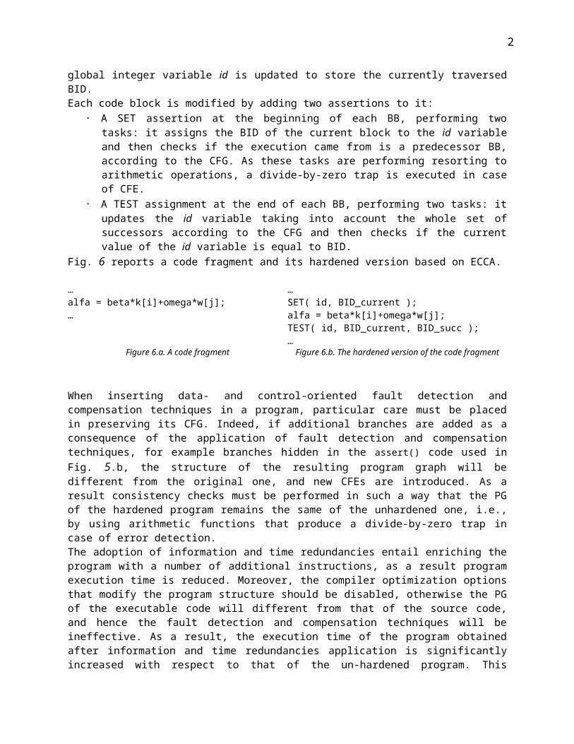
To understand the methods developed to cope with errors affecting the program execution flow (named Control Flow Errors or CFEs), it is important to understand first how to represent the structure of a program.A program code can be partitioned into basic blocks (BBs), which are maximal sequences of consecutive program instructions that, in absence of faults, are always executed altogether from the first to the last. A BB does not contain any instruction changing the sequential execution, such as jump or call instructions, except for the last one. Furthermore, no instructions within the BB can be the target of a branch, jump or call instruction, except for the first one. A BB body corresponds to the BB after the removal of the last jump instruction, if this is a jump instruction. Any program P can be represented with a Control Flow Graph (CFG) composed of a set of nodes V and a set of edges B, P = {V, B}, where V = {v1, v2, …, vn} and B = {bi1,j1, bi2,j2, …, bim,jm}. Each node viV corresponds to a BB. Each edge bi,jB corresponds to the branch from node vi to node vj. Considering the CFG P = {V, B}, for each node vi we define suc(vi) as the set of BBs which are successors of vi and pred(vi) as the set of BBs which are predecessors of vi. A BB vj belongs to suc(vi) if and only if bi,j B. Similarly, vj belongs to pred(vi) if and only if bj,i B.A branch bi,j is illegal if bi,j B. If a fault causes the program to execute a branch b i,kB instead of the correct branch bi,j, then the branch bi,k is wrong. Illegal and wrong branches represent CFEs.All instruction-level techniques to detect CFEs are based on the idea of adding instructions to verify whether transitions among BBs are consistent with the CFG (Golubeva et al., 2006). We can consider the method named Enhanced Control flow Checking using Assertions (ECCA) as an example of this idea.ECCA assigns a unique prime number identifier (the Block Identifier or BID) greater than 2 to each BB of a program. During program execution the global integer variable id is updated to store the currently traversed BID.Each code block is modified by adding two assertions to it:
· A SET assertion at the beginning of each BB, performing two tasks: it assigns the BID of the current block to the id variable and then checks if the execution came from is a predecessor BB, according to the CFG. As these tasks are performing resorting to arithmetic operations, a divide-by-zero trap is executed in case of CFE.
· A TEST assignment at the end of each BB, performing two tasks: it updates the id variable taking into account the whole set of successors according to the CFG and then checks if the current value of the id variable is equal to BID.
Fig. 6 reports a code fragment and its hardened version based on ECCA.

1
…alfa = beta*k[i]+omega*w[j];…
…SET( id, BID_current );alfa = beta*k[i]+omega*w[j];TEST( id, BID_current, BID_succ );…
Figure 6.a. A code fragment Figure 6.b. The hardened version of the code fragment
When inserting data- and control-oriented fault detection and compensation techniques in a program, particular care must be placed in preserving its CFG. Indeed, if additional branches are added as a consequence of the application of fault detection and compensation techniques, for example branches hidden in the assert() code used in Fig. 5.b, the structure of the resulting program graph will be different from the original one, and new CFEs are introduced. As a result consistency checks must be performed in such a way that the PG of the hardened program remains the same of the unhardened one, i.e., by using arithmetic functions that produce a divide-by-zero trap in case of error detection.The adoption of information and time redundancies entail enriching the program with a number of additional instructions, as a result program execution time is reduced. Moreover, the compiler optimization options that modify the program structure should be disabled, otherwise the PG of the executable code will different from that of the source code, and hence the fault detection and compensation techniques will be ineffective. As a result, the execution time of the program obtained after information and time redundancies application is significantly increased with respect to that of the un-hardened program. This problem can be partially solved by demanding some of the operation of the robust program to special-purpose hardware, which is in charge of accelerating the most recurring (and thus time consuming) operations that information and time redundancies perform (Bernardi et al., 2006).An example of real-life application of instruction-level redundancy can be found in the Proton series of single board computers manufactures by SpaceMicro (www.spacemicro.com), which exploits the patented Time Triple Modular Redundancy (TTMR). According to TTMR, each instruction is executed twice, being A1 and A2 the two instances of instruction A, and the two results compared. In case of mismatch, a third instance A3 of the instruction is executed, and the result to be committed to the rest of the application is obtained by majority voting among the results of A1, A2, and A3.
3.2.1.3.2. Task-level redundancyTask-level redundancy techniques combine data- and control-oriented fault detection and compensation techniques by executing twice the same task, and then comparing the obtained results. In case of single-core processor, the two instances of the same task are executed serially, while in case of dual-core processors, they can be executed concurrently.An example of task-level redundancy can be found in the DMT architecture (Pignol, 2006). A single-core processor executes two instances of the same task, which are assigned to two different, not overlapping, and isolated memory spaces. When the results of the two tasks are available, a hardware module compares them, and in case of mismatch resets the processor, and force a new execution of the whole process.
3.2.1.4. Fault coverage and overhead analysisWhen considered the fault coverage capabilities of the different techniques we can conveniently talk about fault detection, defined as the percentage of faults the method is able to detect over the faults that may hit the processor, and fault correction, as the percentage of faults the method is able to recover from over the faults that may hit the processor. In Table 1, we report a fault coverage analysis for different techniques, assuming that a processor such as the PPC750FX is considered. Faults in the memory

1
elements not protected by parity or ECC are considered, only (i.e., faults in user registers and control registers and faults in cache memory are neglected).When analyzing the overhead of the considered techniques we should take into account the hardware overhead (e.g., the number of additional processors, and the area of the additional hardware expressed as a fraction of the processor area), the additional memory occupation, and the additional program execution time. Table 1 compares the overhead of the different architecture normalized versus a system that does not include error detection and compensations techniques. For computing the figures we assume a complex processor like PPC750FX, whose area is notably bigger than that of additional hardware that may be needed by fault detection and compensation techniques.
Technique Fault detection[%]
Fault correction
[%]
Area occupation[#]
Memory occupation
[#]
Execution time[#]
None (original system) <10 0 100 100 100Passive redundancy (TMR) to perform error masking 100 100 <305 <105 <105
Active redundancy (lockstep, with checkpoint executed only in correspondence of 10% of memory accesses) to perform error detection and removal
100 98 <210 <205 <220
Active redundancy (DT2) to perform error detection and removal 100 100 <205 <205 <210
Instruction-level redundancy, with data- and control-oriented techniques to perform error detection only
100 0 100 <400 <300
Instruction-level redundancy, with data- and control-oriented techniques+hardware acceleration to perform error detection only
100 0 <110 <210 <205
Task-level redundancy (DMT) to perform error detection and removal 100 100 <110 <210 <400
Table 1. Overhead comparison
As far as the fault coverage is concerned, we can see that even the original, not robust, system is able to detect some of the faults that radiations may induce. Indeed, processors normally embed some error detection features (beside parity or ECC for memory banks like caches) that can provide partial transient error detection. As an example some faults may be detected through processor traps (e.g., invalid op-code trap). All methods offer complete fault coverage, thus guaranteeing at least the capability of recognizing an improper processor behavior. Among the methods that offer fault compensation, fault correction is at least 98%, thus guaranteeing the possibility of resuming the correct operations upon fault detection of the vast majority of faults.As far as area occupation is considered, all methods except purely-software ones entail some additional hardware, with complexity ranging from small watchdog up to one or two instances of the original processor.Considering memory occupation, purely-software techniques are the most demanding ones, due to the replicated instructions a data. Similarly, software techniques are the most demanding as far as execution time is considered. Other techniques like DT2 and DMT show high execution time overhead, as a slack time equal to the original program execution time (DT2) or twice of the program execution time (DMT) are reserved for error compensation through task re-execution.
3.2.1.5. Final remarks

1
The detection and compensation techniques to be used should be selected on the basis of the application the system is aiming at by evaluating carefully the magnitude of the problem transient faults induce. In certain type of applications transient errors may result in the modification of one pixel, and may occur once every year; as a result, it may be deemed more convenient to avoid any mitigation technique thus saving implementation costs. In other type of application, like the rendezvous with a comet, the system may have to remain operative only few minutes, during which no error is acceptable, otherwise the entire mission is lost; as a result, the most expensive fault detection and compensation technique should be used to guarantee 100% system availability.Moreover, there is not a single best technique that solves all the problems. Certain types of effects induced by transient errors are either too expensive, or impossible to deal with certain techniques, and therefore a mix of different techniques is likely to be the best solution. Therefore, the general architecture of a reliable processor module should entail the processor that executes the application software, possibly enriched with information and time redundancies, plus additional hardware devoted to fault detection and compensation. This module can be as simple as a watchdog timer to reset and wake-up the processor that entered into end-loop due to very critical transient faults, or as complex as the hardware needed for implementing an NMR architecture.
3.2.2. MemoriesMemories are increasingly critical components from the point of view of reliability. Their criticality is due to several factors:
· The high sensitivity of some semiconductor memory technologies (e.g., SRAMs) to radiations; in particular, CMOS based memories are especially prone to radiation-induced errors (Gong, 2003). This is mainly due to the fact that design rules are typically very aggressively pushed when designing memory arrays for area optimization. Moreover, the transistors used in memory cells are often optimized for area and speed and are therefore more sensitive to noise as compared to their logic counterparts.
· The high amount of memory existing in most of today processing systems; many complex Integrated Circuits currently on the market use a high percentage (from 50% to 70%) of the die area for embedded memory cores. It is projected that this percentage will soon increase to 90% of overall chip area on more demanding SoC designs. On the other side, the amount of semiconductor memory existing in most general-purpose systems (e.g., Personal Computers or workstations) already exceeds several GByte even for low-cost products, making the frequency of faults affecting memories extremely high.
For the above reasons, several techniques for detecting and possibly correcting errors affecting memories have been developed in the past decades, and are now commonly adopted in many commercial products, even for non safety-critical applications (Slayman, 2005). However, the choice of the solution which provides the best trade-off between fault detection/correction capabilities, area and performance cost may significantly change from case to case, depending from many factors, such as the application characteristics, the available technology, the environment the product should work in, etc.In the following, a summary of the most common techniques used to protect semiconductor memories against transient faults is presented. We did not consider here solutions based on special memory cells suitable designed for high reliability, which are out of the scope of this chapter.
3.2.2.1. Information redundancy techniquesThis group of techniques is mainly based on error detection and correction codes, which are used extensively in memory arrays in order to reduce the impact of transient errors, whichever their origin. The main idea behind these codes is to use check bits in addition to the data bits to create a checkword. The simplest form of error detection is the use of a parity bit. Each time a word is written to the memory, an extra bit is computed and stored in the memory, which represents the binary sum (or its complement) of all the bits in the word (even or odd parity). If any bit (either in the data part or in the code) is flipped, the

1
parity bit will no longer match the data and an error is detected when the word is read. However, in the case an error is detected the technique cannot provide the information about which bit has been flipped, so the error cannot be corrected.Several solutions exist to implement detection mechanisms based on parity; they differ on which data bits are associated to each parity bit. When the whole memory is composed of different modules in parallel, it may be convenient to associate each parity bit either to a whole word, or to the bits of the word implemented by each module, or to a proper combination of them. The major advantage coming from these schemes, which are summarized in Fig. 7, is that they allow detecting errors arising when a whole memory module becomes faulty. Finally, there have been some efforts to extend the parity method to detection of multiple bits (no matter their multiplicity) by proposing 2D schemes, such as the one shown in Fig. 8 (Pflanz, 2002). The adoption of more check bits per word allows getting more powerful detection and correction codes. Single error correct/double error detection (SEC-DED) codes were first introduced by Hamming (Hamming, 1950) and then continuously improved in the following years (Chen, 1984). The number of check bits required to achieve a given goal (e.g., detection/correction of errors with a given multiplicity) is a function of the size of the data to be protected: this means that the percent area overhead for storing the check bits decreases when the length of the protected word increases. In some cases (e.g., for caches) entire lines are protected with a very reduced number of additional check bits, when compared to the number of data bits. In other cases (e.g., small caches) lines are much smaller, and the overhead required by the codes may be unaffordable: in this case, parity is often adopted, in conjunction with more complex techniques: in some cases, the cache line is simply flushed when an error is detected, and its correct content is then uploaded from memory.
Figure 7. Different parity schemes

1
Figure 8. The cross-parity checking scheme
Double-bit error correction/triple-bit error detection (DEC-TED) is another powerful error correction code. Obviously, the greater error detection/correction capabilities of these codes have a cost in terms of chip area, power required for the extra check bits, and latency for the computation required to encode and decode the check bits each time a word is written/read to/from memory. While sometimes adopted for space applications, DEC-TED codes are not commonly used in terrestrial workstation or server designs for several reasons. First of all, increased computational complexity leads to increased latency. Moreover, none of the word lengths, which minimize the cost for DEC-TED codes, are integral multiples of 8, thus forcing the designer to sub-optimal choices.A further technique which is sometimes used to introduce error detection and correction capabilities to semiconductor memories is based on Reed-Solomon codes. A Reed-Solomon code is characterized by the value of two integer parameters n and k (Blahut, 1983), where n is the number of symbols of m bits (with n ≤ 2m − 1) of a codeword and k is the number of symbols of the related dataword. A Reed-Solomon (n,k) code can correct up to 2E + S ≤ n − k erroneous bits, where E is the number of erasures and S is the number of random errors. An erasure is an error whose location is known a priori (e.g., because it stems from a permanent fault). Transient faults (e.g., SEUs) can occur in unknown locations (i.e., bits) of a codeword; therefore, they can be effectively considered as random errors. Permanent faults (e.g., stuck-at 0/1 cells) can be located using either self-checking circuits, or on-line testing; therefore, they can be effectively considered as erasures.Reed–Solomon coding is commonly used in data transmissions, as well as in mass storage systems to correct the burst errors associated with media defects. Reed–Solomon coding is a key component of the compact disc technology: it has been the first case of adoption of a strong error correction coding technique in a mass-produced consumer product, and DAT and DVD devices use similar schemes.Reed–Solomon coding can also be used to harden semiconductor memories (in particular ROM, RAM and Flash) by adding a proper encoding/decoding circuitry on top of the memory module itself. The adoption of this technique may be convenient when the memory has to be used in particularly harsh environment (e.g., space), and has been boosted by the availability of efficient and compact Intellectual Property cores implementing highly customizable encoder/decoder functions.Error detection latency is a major issue when designing a memory. In fact, latent errors can occur in both SRAM and DRAM due to bad writes (e.g., coming from noise in the system) or cell upsets from alpha particles or cosmic rays. These errors will remain undetected if no reads from the word occur. With a single-bit error already lying dormant, the check word is exposed to the risk of a second bit being upset,

1
leading to an uncorrectable error in an SEC-DED design. In this case, scrubbing (Saleh, 1990) can be successfully exploited, if the application constraints allow its adoption. Scrubbing is a technique to prevent independent single-bit events from evolving into multibit events in memories: it is based on periodically checking (or scrubbing) the memory for correctable errors by traversing the entire address space. In the case of parity-protected caches, if a parity error is encountered, the data would be flushed and a re-read of correct data from main memory would occur. For SEC-DED-protected memory, a single-bit error would be detected and corrected. The probability of two statistically independent single-bit errors affecting the same word is inversely proportional to the time allowed for them to combine (i.e., the time between scrubs). Scrubbing eliminates this risk by removing the first error before the second one can arise. Clearly, scrubbing may significantly reduce the probability of failures by introducing some performance related to the time cost of the periodic scrubbing procedure.
3.2.2.2. Hardware redundancy techniquesThe usage of triple modular redundancy even for memories is not uncommon for mission-critical avionic and space applications. On the other side, this technique is seldom used within commercial servers and workstations (and more in general for ground-level applications) because of the obvious power and area penalties. In almost all cases, judicious use of a ECC-protected cache and memory, combined with a good analysis of the Soft Error Rate (SER) of the different components, a careful design of logic elements, and a correct process-technology selection should be sufficient for commercial designs.
3.2.3. Random logic As described in the previous subsections, plenty transients effects may corrupt the circuits functionalities. Particular SEU and SET tolerance techniques must be taken in account in the design of fault tolerant integrated circuits.
3.2.3.1. Hardware redundancyHardware redundancy solutions can be adopted to protect the logic against transient faults. A commonly adopted solution is the Triple Modular Redundancy (TMR) which is generally used to provide design hardening in the presence of SEUs. All the circuit’s flip-flops are replicated three times and a voter structure is used to the majority of the outputs, accordingly to the TMR scheme. The classical TMR scheme has been proved to be effective in protecting sequential logic against SEUs, nevertheless it brings high overhead on area. TMR techniques are based on the idea that a circuit can be hardened against SEUs or SETs by designing three copies of the same circuit and building a majority voter on the output of the replicated circuit. Implementing triple redundant circuits against SEU effects is generally limited in protecting only the memory elements. Conversely, in case SETs effects are addressed, full module redundancy is required because all the components such as memory elements, interconnections and combinational gates are sensible to SETs. This means that three copies of the user’s design have to be implemented to harden the circuit against SEUs. All the logic resources are triplicated in three different domains according to the traditional TMR approach and voter elements are included at the domain’s outputs. When any of the design domains fails, the other domains continue to work properly, and thanks to the voter, the correct logic passes to the circuit output. The TMR traditional architecture presents two major drawbacks : 1. The design is still vulnerable to SEUs in the voting circuitry. Nevertheless radiation-hardened voting
circuits are available to protect against the permanent damaging of the voter induced by Single-Event Latch-Up (SEL), the CMOS devices adopting physical layout geometries smaller than 0.25 µm are still susceptible to transient effects.
2. There is no protection against the accumulation of SEUs in Flip-Flops (FFs). After an SEU happens, in the traditional TMR scheme, while the state machine is corrected through scrubbing, the state remains un-reset for the synchronization.

1
Figure 9. TMR architecture based on majority and minority voters
In order to protect the voters and input signals, all inputs, outputs and voters are triplicated, which avoid the presence of single points of failure. Besides, in order to ensure constant synchronization between the redundant state registers, majority voters with feedback paths are inserted. The resulting feedback logic of each state machine becomes a function of the current state voted from all the three state registers. The presence of the minority voters allow to protect the circuit outputs from SEUs affecting their resources, that represent a critical point, since they are directly connected to the device pins, as illustrated in figure 9. The full TMR solution could not be the most harden solutions if critical harsh environments are considered. In details, if an higher level of protection against SEUs is necessary, several voter levels can be introduces into the circuit’s random logic in order to increase the protection against transient effects. Nevertheless these solutions introduce an high routing congestion due to the interconnections coming from three domains to a single logic element. This has a severe impact on the delay of a design and the performance degradation may vary from 1.5 and 2.5 times with respect to the original un-hardened circuits.A different solution, that reduces the dramatic overhead of TMR, is the Double Modular Redundancy (DMR). The main characteristic of DMR are the duplication of the storage cells and the correction elements used to output and keep the correct value of the redundant storage cells. The impact of the DMR structure on the area and on the delay is lower than TMR, while the tolerance to SEU effect has similar level, in particular when sequential logic circuits are considered. The principal DMR structure consists in doubling the storage cells of each bit and connecting the replicated outputs to the correction element. In case one of the redundant cells is changed by an SEU, the output of the correction element will maintain the right value. Then, at the next clock’s edge, both the doubled storage cells will latch new data removing the possible errors. The DMR hardening solution allows saving one storage cell for each bit, therefore it is quite obvious that the area and the latency of the correction element is much less than a TMR-based voter. As a drawback, the DMR requires a physical design of the correction element, since the correction element used in DMR solution is a modified inverted latch, since the standard (symmetric) element are not able to decrease the SEU probability.
3.2.3.2. Temporal redundancyThe traditional TMR structure that triplicates only the flip-flops can protect sequential logic against SEUs, however it cannot tolerate transient effects such as SETs in combinational logic. While a possible solution is to triplicate also the combinational paths, thus implementing a full-TMR approach, it does not protect completely the implemented circuits, since a SET glitch may pass through logic states and if multiple glitches arrive at the input of registers exactly at the clock edge, the redundant storage cells would latch incorrect values or go to undefined and metastable states. Therefore particular techniques
2
have been developed to face SET effects. There are two common methods used for SET tolerant circuits, both are based on temporal concepts, pure temporal redundancy approach and SET filter. The temporal redundancy (Mavis, 2002) is based on the TMR structure but it uses three shifted clocks to sample data at different time intervals. The approach is valid in case the SET glitches are shorter than the time interval, since at most one latch would sample incorrect value. A voter is used to forward the correct value to the output latch controlled by another clock domain. The SET filter techniques are based on delaying the signals between sequential elements (Mongkolkachit, 2003). The idea behind SET filtering is to double the logical paths defining two signals: the original signal and the delayed signal, which are connected to the same correction element (which generally consists of a guard gate). Therefore SET pulses having a width shorter than the delay between the two signals would not be able to change the output of the correction element. In relation to the SET filtering, a particular kind of flip-flop has been developed: the DF-DICE cell structure is proposed to improve the aforementioned SET filter technique (Naseer, 2005).Innovative techniques based on the broadening and filtering capabilities of logic gates are currently under evaluation. The idea behind such techniques is based on preventing the effect of propagation of SETs in combinatorial circuits. Two approaches are nowadays proposed: the first is oriented in the modification of the gate design to present balanced high to low and low to high propagation delays (Kastensmidt Lima, 2008), the second is oriented to the modification of the routing electrical characteristics by modifying the placement position of each logic cell within the integrated circuits. Both the approaches presented encouraging results.
4. CONCLUSIONSThe increasing usage of electronic systems for safety critical applications, and the growing sensitivity of semiconductor technologies to transient faults pushed towards the development of different techniques for developing devices and systems able to tolerate such a kind of faults. This chapter provides an overview of the main techniques that have been proposed and/or adopted for processors, memories and logic components. It is up to the designer, based on the specific constraints of its application and design flow, to combine and implement them in the proper way.
REFERENCES
Abate, F., Sterpone, L. & Violante, M. (2008). A New Mitigation Approach For Soft Errors In Embedded Processors. IEEE Transactions on Nuclear Science, 55(4), 2063-2069.Barak, J., Levinson, J., Victoria, M. & Hajdas, W. (1996). Direct process in the energy deposition of protons in silicon. IEEE Transactions on Nuclear Science, 43(6), 2820-2826Barth, J.L., Dyer, C.S. & Stassinopoulos, E.G. (2004). Space, Atmospheric, and Terrestrial Radiation Environments. IEEE Transactions on Nuclear Science, 50(3), 466-482Baumann R. C. (2005). Single events effects in advanced CMOS Technology. IEEE Nuclear and Space Radiation Effects Conference Short Course Textbook.Bernardi, P., Veiras Bolzani, L.M., Rebaudengo, M., Sonza Reorda, M., Vargas, F.L. & Violante, M. (2006). A New Hybrid Fault Detection Technique for Systems-on-a-Chip. IEEE Transactions on Computers, 55(2), 185-198.Blahut, R. E. (1983). Theory and Practice of Error Control Codes. Addison-Wesley Publishing Company.Chen, C. L. & Hsiao, M. Y. (1984). Error-correcting codes for semiconductor memory applications: A state-of-the-art review. IBM J. Res. Develop., 28(2), 124–134.Dodd, P.E. & Massengill, L. W. (2004). Basic Mechanism and Modeling of Single-Event Upset in Digital Microelectronics. IEEE Transactions on Nuclear Science, 50(3), 583-602.Ferlet-Cavrois, V., Paillet, P., McMorrow, D., Fel, N., Baggio, J., Girard, S., Duhamel, O., Melinger, J.S., Gaillardin, M., Schwank, J.R., Dodd, P.E., Shaneyfelt, M.R. & Felix, J. A. (2007). New insights into

2
single event transient propagation in chains of inverters-evidence for propagation-induced pulse broadening. IEEE Transactions on Nuclear Science, 54(6), 2338-2346.Golubeva, O., Rebaudengo, M., Sonza Reorda, M. & Violante, M. (2006). Software-Implemented Hardware Fault Tolerance. Springer.Gong, M.K. et al. (2003). Modeling Alpha-Particle-Induced Accelerated Soft Error Rate in Semiconductor Memory. IEEE Transactions on Electronic Devices, 50(7), 1652-1657.Hamming, R. W. (1950). Error detecting and error correcting codes. Bell Syst.Tech. Journal, 29(2), 147–160, 1950.Kastensmidt Lima, F., Wirth, G., Ribeiro, I. (2008) Single Event Transients in Logic Circuits-Load and Propagation Induced Pulse Broadening, 55(6), 2928-2935.May, T.C. & Woods, M.H. (1979). Alpha-particle-induced soft errors in dynamic memories. IEEE Transactions on Electronic Devices, 26(2), 2-9.Mavis, D.G. & Eaton, P.H. (2002). Soft error rate mitigation techniques for modern microcircuits. Reliability Physics Symposium Proceedings, 40th Annual, 216-225.Mongkolkachit, P. & Bhuva, B. (2003). Design technique for mitigation of alpha-particle-induced single-event-transients in combinational logic. IEEE Transactions on Device and Material Reliability, 3(3), 89-92.Naseer, R. & Draper J. (2005). The DF-DICE storage element for immunity to soft errors. In proceedings IEEE Midwest Symposium on Circuits and Systems.Pflanz, M., Walther, K., Galke, C. & Vierhaus, H.T. (2002). On-Line Error Detection and Correction in Storage Elements with Cross-Parity Check. Proceedings of the Eighth IEEE International On-Line Testing Workshop, 69-73.Pignol, M. (2006) DMT and DT2: Two Fault-Tolerant Architectures developed by CNES for COTS-based Spacecraft Supercomputers. In Proceedings of the 12 th IEEE International On-Line Testing Symposium, 203-212.Pradhan, D.K. (1996). Fault-Tolerant Computer System Design. Prentice Hall.Rajeevakumar, T. V., Lu, N., Henkels, W., Hwang, W. & Franch R. (1988) A new failure mode of radiation-induced soft errors in dynamic memories. IEEE Electronic Device Letters, 9(12), 644-646.Saleh, A. M., Serrano, J. J. & Patel, J. H. (1990). Reliability of scrubbing recovery-techniques for memory systems. IEEE Transactions on Reliability, 39 (1), 114–122, 1990.Slayman, C.W. (2005). Cache and Memory Error Detection, Correction, and Reduction Techniques for Terrestrial Servers and Workstations. IEEE Transactions on Device and Materials Reliability, 5(3), 2005, 397-404.Sterpone, L., Battezzati, N., Ferlet-Cavrois, V. (2009) Analysis of SET Propagation in Flash-based FPGAs by means of Electrical Pulse Injection. IEEE Radiaction Effects on Component and Systems, 2009.Taber, A.H. & Normand, E. (1995). Investigations and characterization of SEU effects and hardening strategies in avionics, Alexandria, A: Defense Nuclear Agency.Troutman, R.R. (1983). Epitaxial layer enhancement of n-well guard rings for CMOS circuits. IEEE Electron Device Letters, 4(12), 438-440.
KEY TERMS
Transient faults, Error Detection, Redundancy, Error Correction, Single Event Upsets, Single Event Effects, Single Event Transients, Multiple Event Upsets.