Advanced solutions for HDD head and media manufacturing · Advanced solutions for HDD head and...
16
Advanced solutions for HDD head and media manufacturing E. Noel Abarra Canon ANELVA Corporation 2-5-1 Kurigi, Asao-ku, Kawasaki-shi Kanagawa 215-8550, JAPAN (Sept. 2007)
Transcript of Advanced solutions for HDD head and media manufacturing · Advanced solutions for HDD head and...

Advanced solutions for HDD head and media manufacturing
E. Noel AbarraCanon ANELVA Corporation2-5-1 Kurigi, Asao-ku, Kawasaki-shiKanagawa 215-8550, JAPAN(Sept. 2007)
2/16
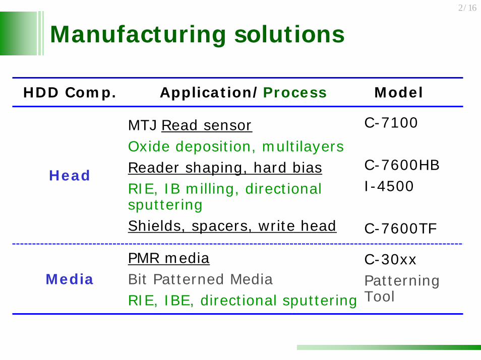
Manufacturing solutions
HDD Comp. Application/Process
Head
MTJ Read sensorOxide deposition, multilayersReader shaping, hard biasRIE, IB milling, directional sputteringShields, spacers, write head
PMR mediaBit Patterned MediaRIE, IBE, directional sputtering
Media
Model
C-7100
C-7600HBI-4500
C-7600TF
C-30xxPatterning Tool

3/16
Read-sensor deposition
20 Å
Up to 8” diameter waferThickness uniformity ≤ 0.5%, 1σPrecise thickness control ≤ 0.1ÅUHV base pressure ≤ 5×10⁻⁹ TorrLow pressure sputteringSmall target sizeCo-sputtering capabilityProprietary processes
Y. Nagamine, et al., Appl. Phys. Lett. 89, 162507 (2006).
MgO-based MTJ
C-7100MRAM film fabrication standard.

4/16
Hard bias fabrication
Al2O3
TaCoPt
Cr
1. TMR dep. + Ta mask + PR
2. RIE + ashing(+ IBE)
3. Insulator dep. 4. Hard bias dep. +cap layer
PCM (directional sputtering)RIE, IBEC-7100
C-7600HB with RIE, IBE and iPVDcapabilities; all without breaking vacuum.

5/16
TMR patterning and HB deposition
Center
IBE/RIE shaping of TMR Nordiko (NTSL) broad ion beam
technology.MICP – high taper angle etch methanol RIE.
Uniform RA; no corrosion or side wall re-deposition.
Hard bias depositionUniform thickness, directional PVD on patterned wfrs (5~8”).
Small targets (7”), high HCfilms.
C-7600HB
Edge

6/16
Hard bias formation
7600HB RIE-PCM IBE-IBD
Throughput 2~3× higher low IBD deposition rate
Etching features
clean, no shorts, high selectivity
wall re-deposition, possible shorts, poor selectivity
Etch angle70-80° withmetal mask
shallow
In-board/Out-board symmetric deposition
present due to incidence angle spread
Running costs small targetslarge rectangular targets, expensive Molybdenum grids

7/16
Thick film deposition
MR shields
trailing shieldwrite pole
10 µm
insulating spacer1PVD-EX module (8” wafers):
Uniformity: <1% 1σ (TaN, Ta)Deposition rate: 4~8 Å/sec
C-7600TFRs Uniformity: < 1% Rs Uniformity: <1%

8/16
Al2O3 and SiC insulators
Al2O3 SiC.8 µm3 µm 2
Rate > 15 nm/minUniformity 8” [1σ] < 1%Refractive index ~1.65Substrate T < 80°C
Rate > 11 nm/minUniformity 8” [1σ] < 0.5%Substrate T < 85°C

9/16
Media (Outline)PMR high pressure sputteringBit patterningNew sputtering system
Head (Summary)TMR Reader excellent RA and MRThe hard bias high taper angle, symmetric
deposition, all in vacuo process, low CoO
Thick films excellent uniformity and high throughput

10/16
Rigid Disk Media Manufacturing
C-3040: PMR 1200 pph, >7 days between PM’s
Introduced: Carrier exchangesystem, P0 holder etcher, magnetic cooling, SUL and high pressure process magnet cathodes, 4 cathode rotating module . . .

11/16
High pressure: Erosion profile
(A) Ref.
C
B
A
CB
Nonmagnetic, 9 mm, 5 Pa (37.5 mTorr)
Magnetic granular oxide, 7 mm, 5 Pa (37.5 mTorr)
Target Utilization (%)
> 40% longer operation feasible.
05
10152025303540
A B C

12/16
RIE-processed patterned media
Height: 25-30 nm
MFMAFM
Resist/Ta: 150 nm/15 nm
Resist/Ta: 200 nm/20 nm
MagLayer
Intermediate Layer
(DTM)
T. Shimatsu et al., Tohoku Univ., unpublished.
I-4500MICP RIE
(BPM)
13/16
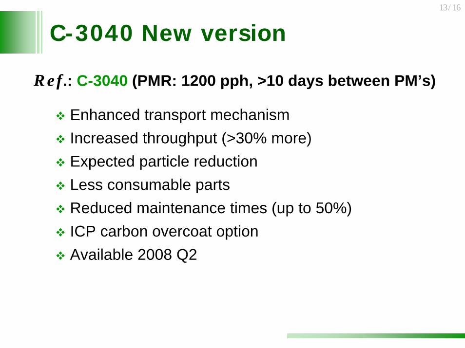
C-3040 New version
Ref.: C-3040 (PMR: 1200 pph, >10 days between PM’s)
Enhanced transport mechanismIncreased throughput (>30% more)Expected particle reductionLess consumable parts Reduced maintenance times (up to 50%)ICP carbon overcoat optionAvailable 2008 Q2

14/16
SummaryHead
TMR Reader leading performanceThe hard bias steep taper angle, symmetric
depositionThick films excellent uniformity and
high throughputMedia
Efficient cathodes for high PAr+M sputteringExperienced in key patterning technologies Enhanced new sputtering system

15/16
Canon ANELVA relocationCome visit us at our new facility.
(3x the floor space of former Fuchu facility)
Kurigi, Kawasaki

16/16
DTR or Bit Patterned MediaHattori et al., IEEE Trans. Magn. vol. 40,
pp. 2510-2515, 2004. photoresist + NILHM etch (RIE, RIBE)hard mask
recording layer
substrateSUL
deposition imprint and patterning
overcoatSiO2 filling planarization (IBE)RL etch (IBE)
pattern etching, deposition, and planarization
Technologies are available in house – and are being integrated.(Canon Anelva provides IBE, dry etch, and directional sputtering tools.)