Digital Integrated Circuits© Prentice Hall 1995 Interconnect COPING WITH INTERCONNECT.
Upload
trinhquynhCategory
view
223download
2
TechSearch International, Inc.
K&S Interconnect Technology SymposiumK&S Interconnect Technology Symposium
Advanced Packaging Interconnect Trends and Technology DevelopmentsE. Jan Vardaman, President, TechSearch International, Inc.
2TechSearch International, Inc.
K&S Interconnect Technology SymposiumK&S Interconnect Technology Symposium
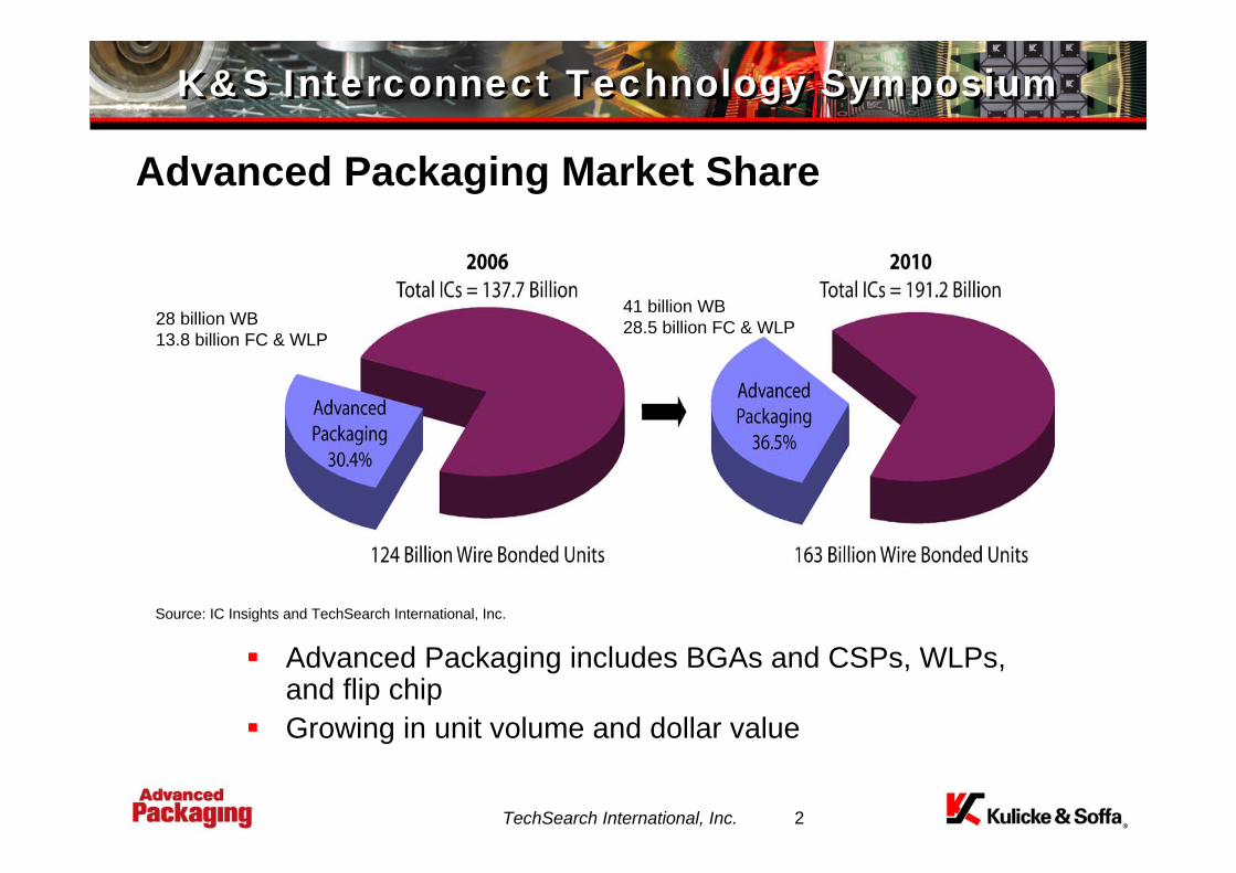
Advanced Packaging Market Share
Advanced Packaging includes BGAs and CSPs, WLPs, and flip chipGrowing in unit volume and dollar value
Source: IC Insights and TechSearch International, Inc.
28 billion WB13.8 billion FC & WLP
41 billion WB28.5 billion FC & WLP

3TechSearch International, Inc.
K&S Interconnect Technology SymposiumK&S Interconnect Technology Symposium
Drivers for Advanced Packaging GrowthMobile phones
More than one billion mobile phones expected to ship in 2007Mobile phones contain an average 15 CSPs, including SiPSiP for digital baseband section, transceiver section, RF section, camera moduleDrives volumes for stacked die packages and system-in-package (SiP)
Portable consumer products (digital camcorders, cameras)Digital cameras/camcorders, MP3 players, DVD players, etc.More than 100 million of Apple’s iPods shipped since 2002Thin is in…..drives new package technology developments
Personal computersPCs highest volume application for PBGAs
Game machinesGrowing volumes for PBGAs and CSPs

4TechSearch International, Inc.
K&S Interconnect Technology SymposiumK&S Interconnect Technology Symposium
Sony’s PS3 with BGAs and CSPs
More than 20 BGAs and CSPsLeadframe parts including QFPs
Source: http://pc.watch.impress.co.jp

5TechSearch International, Inc.
K&S Interconnect Technology SymposiumK&S Interconnect Technology Symposium
Apple’s iPod Nano
At least 7 CSPs on the main board, all wire bondedCSPs are underfilled4 Gbit memory package in a TSOP, mounted on a daughter card2 Gbit memory mounted directly on the board
Source: Adapted from Impress Corporation
Source: Apple Inc.

6TechSearch International, Inc.
K&S Interconnect Technology SymposiumK&S Interconnect Technology Symposium
①
③
④⑤
②
1.200.801.201.01.20PKG Thickness (mm)
37690624257109PIN COUNT
10.0x11.011.0x13.013.0x13.010.0x10.011.5x13.0PKG SIZE (mm)
0.50
FBGA(L)
③
0.500.800.500.80Terminal Pitch (mm)
FBGA(L)FBGA(L)FBGA(L)FBGA(L)PKG TYPE
⑤④②①
Panasonic P901iTV
Source: TPSS

7TechSearch International, Inc.
K&S Interconnect Technology SymposiumK&S Interconnect Technology Symposium
Apple’s iPhone
More than 700,000 iPhones sold during the first weekend ofproduct introductionMany wire bonded parts, a few WLPs
Source: http://www.embedded.com

8TechSearch International, Inc.
K&S Interconnect Technology SymposiumK&S Interconnect Technology Symposium
Apple’s iPhone
QuickTime?and aTIFF (LZW) decompressor
are needed to see this picture.
Intel stacked die package

9TechSearch International, Inc.
K&S Interconnect Technology SymposiumK&S Interconnect Technology Symposium
Apple’s iPhone
Source: http://www.embedded.com
Contains stacked die and PoPSamsung PoP with
processor in the bottom package and two 512 Mbit SRAM die in the top stacked die package
10TechSearch International, Inc.
K&S Interconnect Technology SymposiumK&S Interconnect Technology Symposium
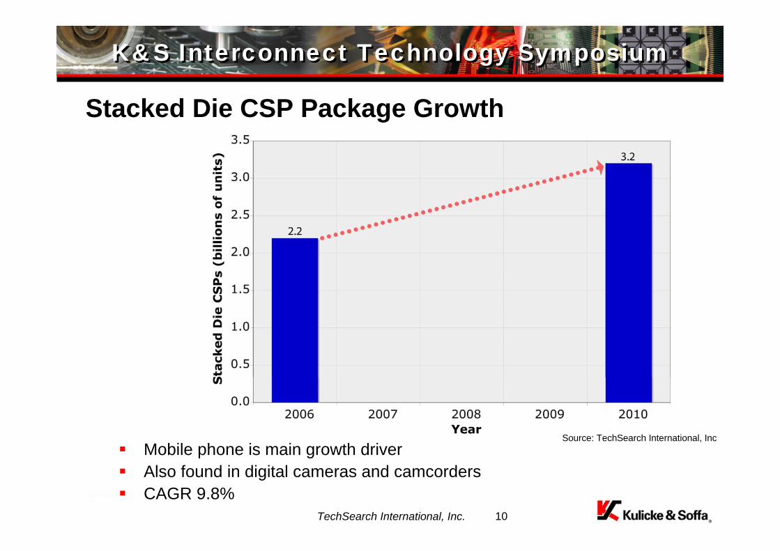
Stacked Die CSP Package Growth
Mobile phone is main growth driverAlso found in digital cameras and camcordersCAGR 9.8%
Source: TechSearch International, Inc

11TechSearch International, Inc.
K&S Interconnect Technology SymposiumK&S Interconnect Technology Symposium
Stacked Die CSPs
16 die stack demonstrated, 4-5 die per package common, typically 2 die per package in today’s productsTypically wire bond, but some gold stud bump (using ball bonder)
Source: Intel
Source: TI
Source: Samsung
12TechSearch International, Inc.
K&S Interconnect Technology SymposiumK&S Interconnect Technology Symposium
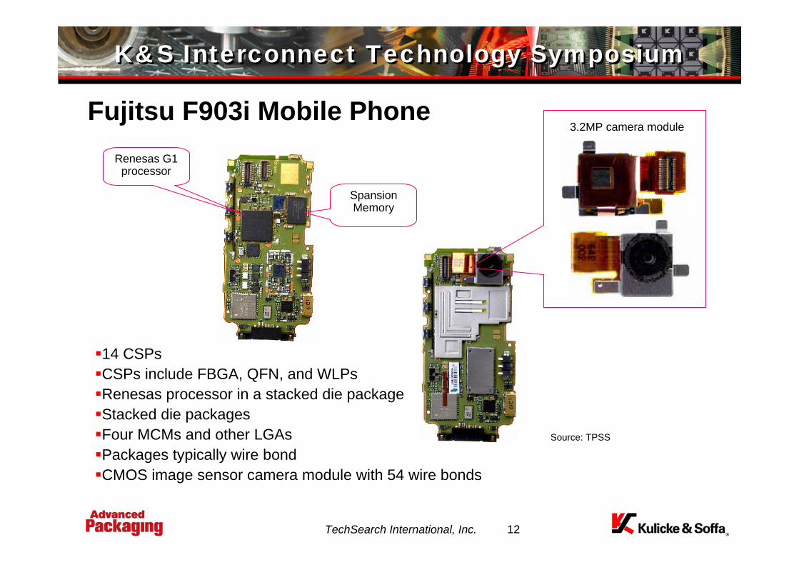
Fujitsu F903i Mobile PhoneRenesas G1
processor
SpansionMemory
14 CSPs CSPs include FBGA, QFN, and WLPsRenesas processor in a stacked die packageStacked die packagesFour MCMs and other LGAsPackages typically wire bondCMOS image sensor camera module with 54 wire bonds
3.2MP camera module
Source: TPSS

13TechSearch International, Inc.
K&S Interconnect Technology SymposiumK&S Interconnect Technology Symposium
Spansion’s Stacked Die in Fujitsu’s F903i
Two die stacked packageHundreds of wire bonds per CSP
Marking 98WS768P0GFA006Body Size 9x13mm
Ball Pitch 0.80mmSubstrate THK 0.25mm
Mold Cap THK 0.79mm
PKG THK except Ball 1.04mm
Bonding Method Wire Bonding
Die Configuration 2 Dies Stacked
Die size (Top die) 6.4x7.4x0.1mm
Die size (Middle die) 9.6x5.3x0.09mm
Die size (Bottom die) 11.7x6.9x0.09mm
Source: TPSS
14TechSearch International, Inc.
K&S Interconnect Technology SymposiumK&S Interconnect Technology Symposium
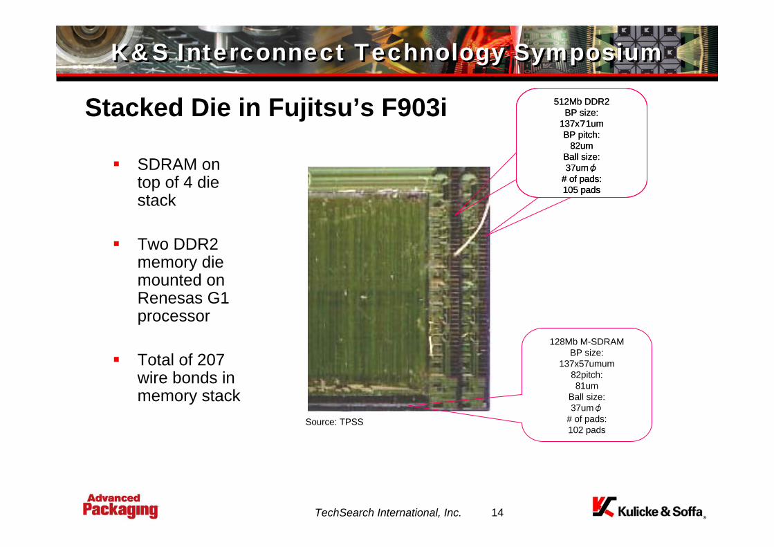
Stacked Die in Fujitsu’s F903i
SDRAM on top of 4 die stack
Two DDR2 memory die mounted onRenesas G1 processor
Total of 207 wire bonds in memory stack
512Mb DDR2BP size:
137x71umBP pitch:
82umBall size:37umφ
# of pads:105 pads
128Mb M-SDRAMBP size:
137x57umum82pitch:81um
Ball size:37umφ
# of pads:102 pads
512Mb DDR2BP size:
137x71umBP pitch:
82umBall size:37umφ
# of pads:105 pads
Source: TPSS
15TechSearch International, Inc.
K&S Interconnect Technology SymposiumK&S Interconnect Technology Symposium
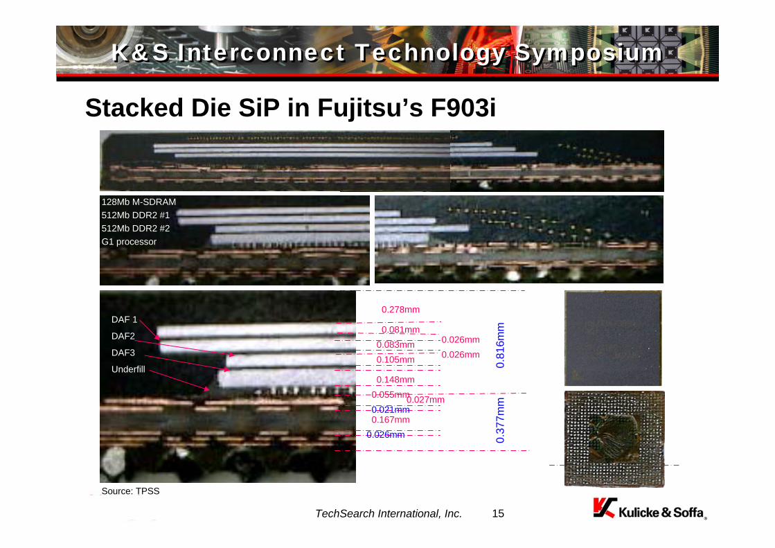
Stacked Die SiP in Fujitsu’s F903i
0.278mm
0.081mm0.026mm0.083mm0.026mm0.105mm
0.148mm0.055mm0.027mm
0.81
6mm
0.37
7mm
0.021mm0.167mm
0.026mm
128Mb M-SDRAM512Mb DDR2 #1512Mb DDR2 #2G1 processor
DAF 1
DAF2
DAF3
Underfill
Source: TPSS

16TechSearch International, Inc.
K&S Interconnect Technology SymposiumK&S Interconnect Technology Symposium
Spansion’s Stacked Die in Fujitsu’s F903i
0.375mm
0.097mm
0.090mm
0.094mm
0.029mm
0.030mm0.050mm
0.74
0㎜0.
253㎜
0.99
6mm
0.024mm0.036mm
0.014mm0.057mm
0.013mm0.033mm
0.027mm
DAF
Insulator
Source: TPSS

17TechSearch International, Inc.
K&S Interconnect Technology SymposiumK&S Interconnect Technology Symposium
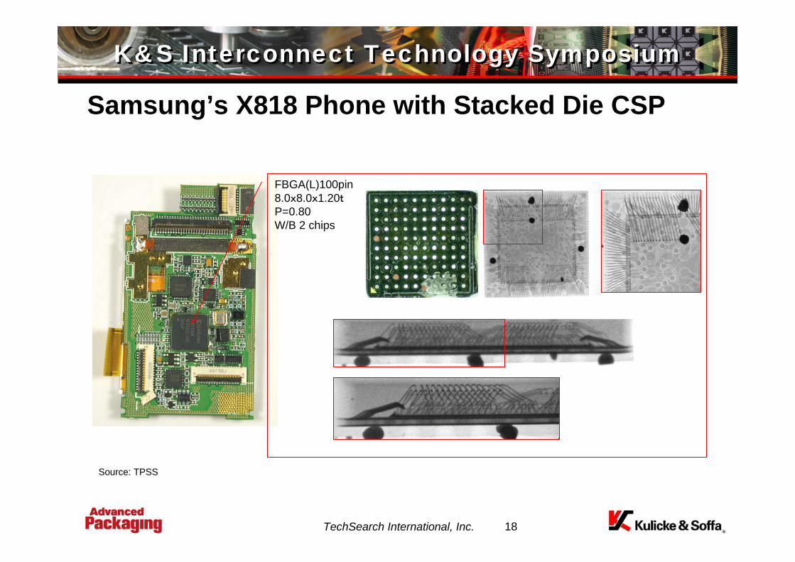
Samsung’s X818 Phone with Stacked Die CSP
Mobile phone for China marketContains 18 CSPs plus several MCMsContains stacked die CSPs
FBGA(L)167pin10.5x14.0x1.40tP=0.80W/B 4 chips
FBGA(L)224pin10.0x10.0x1.20tP=0.50W/B 1chip
FBGA(L)25pin3.0x3.0x0.80tP=0.50W/B 1chip
Source: TPSS
18TechSearch International, Inc.
K&S Interconnect Technology SymposiumK&S Interconnect Technology Symposium
Samsung’s X818 Phone with Stacked Die CSP
FBGA(L)100pin8.0x8.0x1.20tP=0.80W/B 2 chips
Source: TPSS

19TechSearch International, Inc.
K&S Interconnect Technology SymposiumK&S Interconnect Technology Symposium
Spansion’s Roadmap for Die Stacking
Number of die per stack has increased over time, and with it an increase in the number of wiresDie thickness has decreasedAt the same time, pitch has decreased
Source: Spansion

20TechSearch International, Inc.
K&S Interconnect Technology SymposiumK&S Interconnect Technology Symposium
Stacked Die Packaging TrendsStacked Die Packaging Trends
Thinner packagesFrom 1.2, 1.4 mm to below 1 mm.
Higher level stackingFrom 2, 3, 4 level to 5, 6, 7 level stack
Multi-function chipsFrom flash and SRAM to including ASIC and logic
Thinner dieLower loop heightControl of impact when
bonding on overhang
Longer wire lengthLooping sway controlThermal control
Finer pitch

21TechSearch International, Inc.
K&S Interconnect Technology SymposiumK&S Interconnect Technology Symposium
Stacked Die ChallengesWafer thinning/die attach
Thickness of 75 µm in volume production todayDevelopment work with thicknesses of 50 µm in development for both 8-inch and 12-inch wafersMechanical issues with dicing (handling, chipping, flaking)
Wire bondingLow loop heights, reverse bondingSmaller diameter wire, longer spansDie to die wire bonding can be complexDie overhang (spacers required for same size die)
Material selectionSubstrates need to be thin, but rigidMold compound selection
Thermal performanceBusiness issues if logic + memory
LogisticsTesting (KGD)Yield
22TechSearch International, Inc.
K&S Interconnect Technology SymposiumK&S Interconnect Technology Symposium
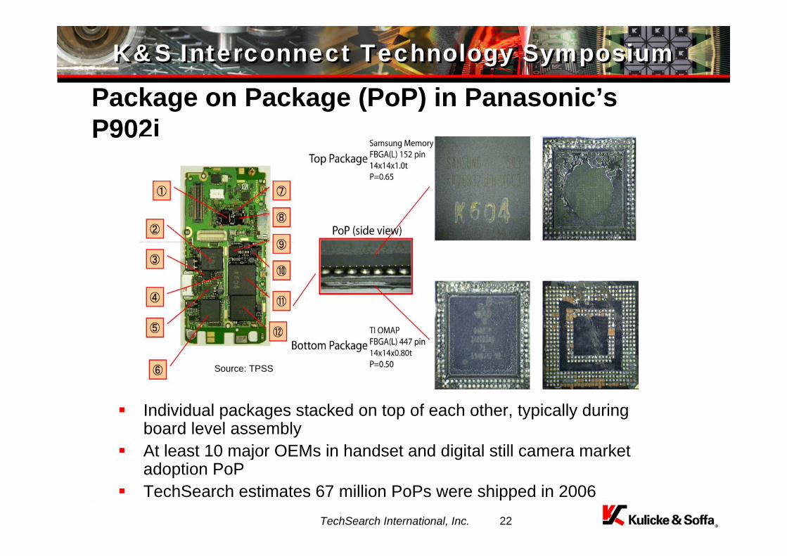
Package on Package (PoP) in Panasonic’s P902i
Individual packages stacked on top of each other, typically during board level assemblyAt least 10 major OEMs in handset and digital still camera market adoption PoPTechSearch estimates 67 million PoPs were shipped in 2006
Source: TPSS

23TechSearch International, Inc.
K&S Interconnect Technology SymposiumK&S Interconnect Technology Symposium
Amkor’s PoP Options
Source: Amkor

24TechSearch International, Inc.
K&S Interconnect Technology SymposiumK&S Interconnect Technology Symposium
SiP Growth
SiP is a functional system or subsystem assembled into a single packageUtilizes combination of advanced packaging such as bare die (wire bond or flip chip), CSP, stacked package, stacked dieCAGR of 15.9%
Source: TechSearch International, Inc.
Cell phonesPDAsMP3 playersCamerasComputersAutomotiveMedicalIndustrialDefenseAerospace

25TechSearch International, Inc.
K&S Interconnect Technology SymposiumK&S Interconnect Technology Symposium
ASE Examples of SiP for Mobile RF
Examples of PA (with antenna and switch), Transceiver, Front-End Module, DCR, SPR, BT, WLANModule package size ranges from 3mm x 3mm to 13mm x 13mmPackage thickness from 0.85 to 1.8 mmDie including silicon (min. 75µm thick), SiGe, GaAs HBT, pHEPT, CMOS,
SAW/BAW filterFine pitch wire bond 45 µm bond pad pitch
Note: DCR (Direct Conversion Receiver), SPR (Single Package radio), pHEMT (Pseudo-morphic High Electron Mobility Transistor), HBT (Hetero-junction Bipolar Transistor), CMOS (Complementary meta-Oxide Semiconductor)
Source: ASE
26TechSearch International, Inc.
K&S Interconnect Technology SymposiumK&S Interconnect Technology Symposium
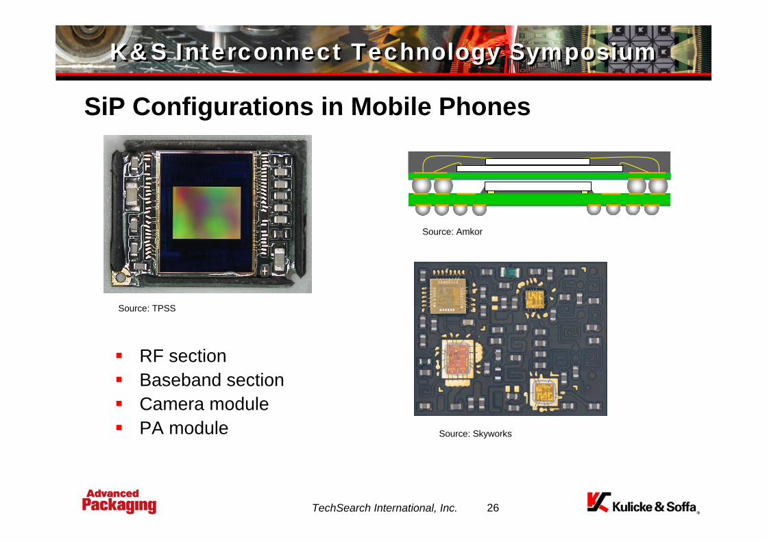
SiP Configurations in Mobile Phones
RF sectionBaseband sectionCamera modulePA module
Source: TPSS
Source: Amkor
Source: Skyworks

27TechSearch International, Inc.
K&S Interconnect Technology SymposiumK&S Interconnect Technology Symposium
Future 3D TSV Camera Modules with Gold Stud Bump
Au stud bump
RIE or Laser Drill
Cu plated via
Al wiring
Stud bump made of Au wire
Stacking cross sectionSource: Hitachi
28TechSearch International, Inc.
K&S Interconnect Technology SymposiumK&S Interconnect Technology Symposium
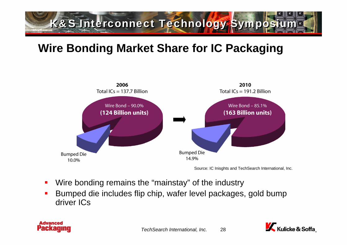
Wire Bonding Market Share for IC Packaging
Wire bonding remains the “mainstay” of the industryBumped die includes flip chip, wafer level packages, gold bump driver ICs
Source: IC Inisghts and TechSearch International, Inc.

29TechSearch International, Inc.
K&S Interconnect Technology SymposiumK&S Interconnect Technology Symposium
Why Doesn’t Flip Chip Dominate the Interconnect World?
Flip Chip is used where needed, for performance or pad limited designs mostly, but in some cases form factor
Continued advances in wire bond technology Flip chip substrates are typically more expensive than wire bond substrates
Wire bond designs typically routed in four layersFlip chip substrates are more complex, route bumped die with fine pitchFlip chip often requires build-up substrates with lower yield, more expensive material sets, greater complexity
Source: ASESource: ChipWorks

30TechSearch International, Inc.
K&S Interconnect Technology SymposiumK&S Interconnect Technology Symposium
Why Doesn’t Flip Chip Dominate the Interconnect World?
Many companies have found that flip chip assembly is typically more expensive than wire bond
Flip chip substrate shortage in 2005 increased substrate prices, with current overcapacity substrate prices are falling againIntel has twice delayed the move from wire bond to flip chip for the ICH chipset (Southbridge), current delay shifts flip chip adoption out to 2009Estimated assembly cost for wire bond vs. flip chip in large die size 17mm x 17mm found flip chip assembly was 30% more expensive than wire bond (even without consideration of substrates)

31TechSearch International, Inc.
K&S Interconnect Technology SymposiumK&S Interconnect Technology Symposium
Wire Bond Pitch Trends (actual production)
Wire bond pitch in actual production has become finer and finer over time, trend continues
Source: TechSearch International, Inc.

32TechSearch International, Inc.
K&S Interconnect Technology SymposiumK&S Interconnect Technology Symposium
Bond Pad Over Active I/OLSI developed the industry’s first wire bond over active I/O technology (Pad on I/O™) for copper/low-kAllows the extension of wire bond technology to deep submicron CMOS designs in 130nm and 90nm nodes that are typically pad limitedPlacing wire bonds over the active I/O saves die area and does not affect metal routing and interconnectCan be used for in-line or staggered pad designs (27µm effective)
Source: LSI

33TechSearch International, Inc.
K&S Interconnect Technology SymposiumK&S Interconnect Technology Symposium
New Developments in Low Loop Height Wire Bonding
Specially designed for stacked die applicationsHighly accurate and consistent loop profilesImproved loop linearity and stabilityHigher bond test results
Source: K&S

34TechSearch International, Inc.
K&S Interconnect Technology SymposiumK&S Interconnect Technology Symposium
Die to Die Bonding65 µm bonding pad pitch Min.55 µm bond pad open Min.
Wire Length
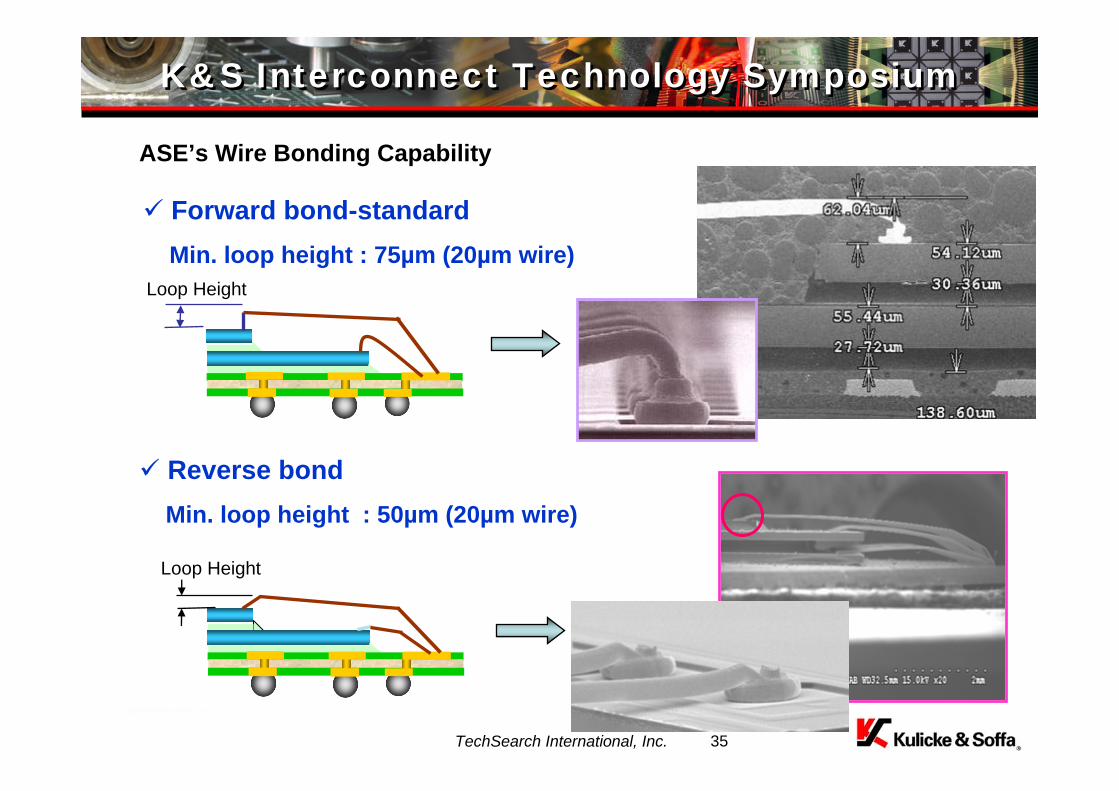
ASE’s Wire Bonding Capability
Max. Wire Length (MWL) Wire Diameter Bond PadOpening
3.8mm(150mil)< MWL ≦ 4mm(160mil) 30um(1.2mil) B.P.O.≧80(um)
3.5mm(140mil) < MWL ≦ 3.8mm(150mil) 28um(1.1mil) B.P.O.≧63(um)
3.3mm(130mil)< MWL ≦ 3.5mm(140mil) 25um(1.0mil) B.P.O.≧53(um)
3mm(120mil) < MWL ≦ 3.3mm(130mil) 23um(0.9mil) B.P.O.≧43(um)
MWL ≦3mm(120mil) 20um(0.8mil) B.P.O.≧40(um)
Long length capability
35TechSearch International, Inc.
K&S Interconnect Technology SymposiumK&S Interconnect Technology Symposium
ASE’s Wire Bonding Capability
Forward bond-standard Min. loop height : 75µm (20µm wire)
Loop Height
Reverse bond Min. loop height : 50µm (20µm wire)
Loop Height
36TechSearch International, Inc.
K&S Interconnect Technology SymposiumK&S Interconnect Technology Symposium
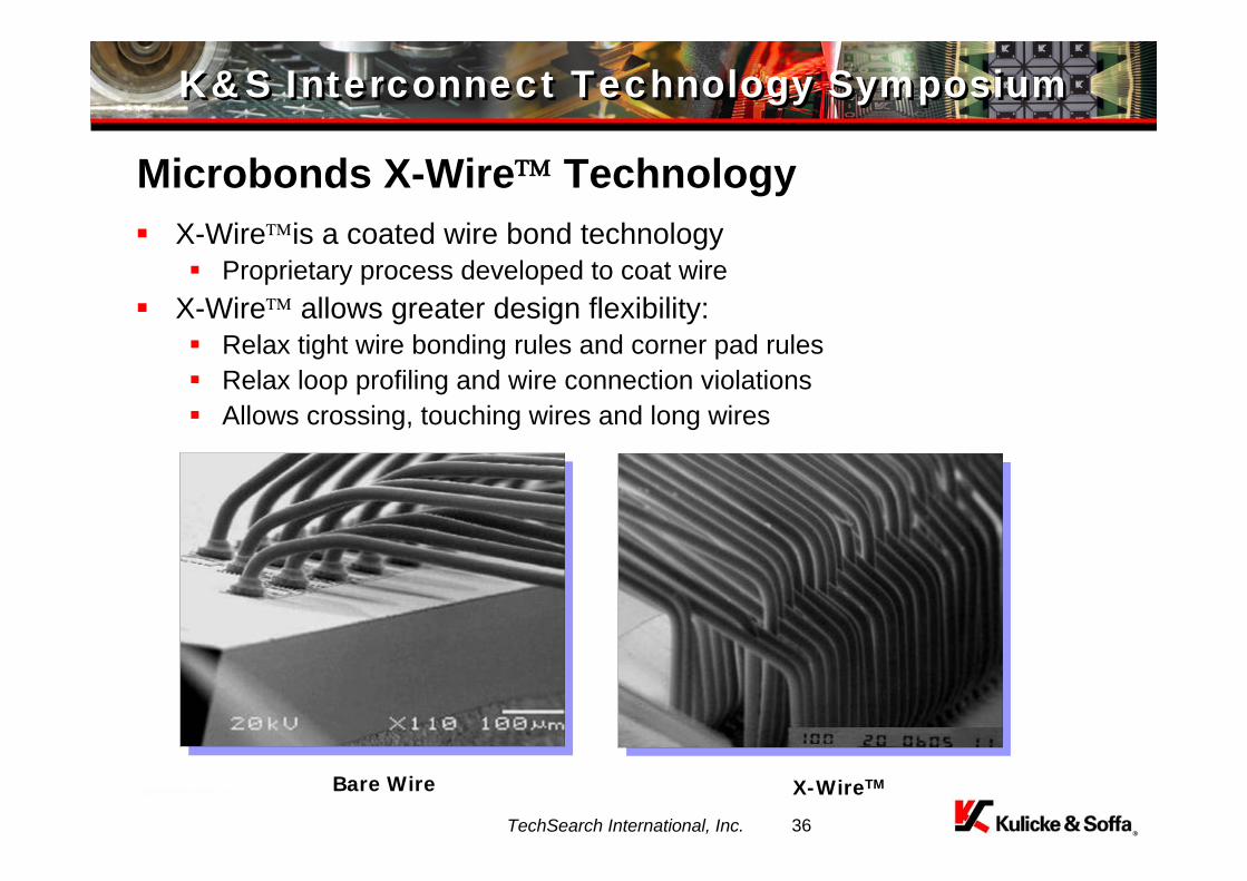
Microbonds X-Wire™ TechnologyX-Wire™is a coated wire bond technology
Proprietary process developed to coat wireX-Wire™ allows greater design flexibility:
Relax tight wire bonding rules and corner pad rulesRelax loop profiling and wire connection violationsAllows crossing, touching wires and long wires
Bare Wire X-WireTM

37TechSearch International, Inc.
K&S Interconnect Technology SymposiumK&S Interconnect Technology Symposium
ConclusionsAdvanced packaging continues to grow in units and revenue
IC package subcontractors improve revenue growth with advanced package assembly
Advanced packaging ≠ FCWire bond accounts for 90% of IC packages shipped in 2006Advanced packaging includes BGAs, CSPs, flip chip, and wafer level packages
Wire bond accounts for 67% of all advanced packagesStrong unit volume growth in a variety of packages including stacked die, SiP, BGA, and all types of CSPs
38TechSearch International, Inc.
K&S Interconnect Technology SymposiumK&S Interconnect Technology Symposium
Company Copyright
This PowerPoint presentation
and all of its contents are protected under
International and United States Copyright laws.
Any reproduction or use of all or any part
of this presentation without the express
written consent of K&S is prohibited.