
Advanced Nanoscale ULSI Interconnects: Fundamentals...
30
Advanced Nanoscale ULSI Interconnects: Fundamentals and Applications
Transcript of Advanced Nanoscale ULSI Interconnects: Fundamentals...

Advanced Nanoscale ULSI Interconnects:Fundamentals and Applications
Yosi Shacham-Diamand · Tetsuya Osaka ·Madhav Datta · Takayuki OhbaEditors
Advanced Nanoscale ULSIInterconnects: Fundamentalsand Applications
123
EditorsYosi Shacham-DiamandTel Aviv University69978 Ramat Aviv, Tel [email protected]
Madhav DattaCooligy, Inc.2370 Charleston RoadMountain View CA [email protected]
Tetsuya OsakaDepartment of Applied ChemistryWaseda University3-4-1 OkuboTokyoShinjuku-ku [email protected]
Takayuki OhbaDivision of Corporate RelationsThe University of Tokyo7-3-1 HongoTokyoBunkyo-ku [email protected]
ISBN 978-0-387-95867-5 e-ISBN 978-0-387-95868-2DOI 10.1007/978-0-387-95868-2Springer New York Dordrecht Heidelberg London
Library of Congress Control Number: 2009934298
© Springer Science+Business Media, LLC 2009All rights reserved. This work may not be translated or copied in whole or in part without the writtenpermission of the publisher (Springer Science+Business Media, LLC, 233 Spring Street, New York,NY 10013, USA), except for brief excerpts in connection with reviews or scholarly analysis. Use inconnection with any form of information storage and retrieval, electronic adaptation, computer software,or by similar or dissimilar methodology now known or hereafter developed is forbidden.The use in this publication of trade names, trademarks, service marks, and similar terms, even if they arenot identified as such, is not to be taken as an expression of opinion as to whether or not they are subjectto proprietary rights.
Printed on acid-free paper
Springer is part of Springer Science+Business Media (www.springer.com)

This book is dedicated to my wife Anat for all hersupport and patience.

Preface
In Advanced ULSI interconnects – fundamentals and applications we bring acomprehensive description of copper-based interconnect technology for ultra-large-scale integration (ULSI) technology for integrated circuit (IC) application. Inte-grated circuit technology is the base for all modern electronics systems. You canfind electronics systems today everywhere: from toys and home appliances to air-planes and space shuttles. Electronics systems form the hardware that together withsoftware are the bases of the modern information society. The rapid growth andvast exploitation of modern electronics system create a strong demand for new andimproved electronic circuits as demonstrated by the amazing progress in the fieldof ULSI technology. This progress is well described by the famous “Moore’s law”which states, in its most general form, that all the metrics that describe integratedcircuit performance (e.g., speed, number of devices, chip area) improve exponen-tially as a function of time. For example, the number of components per chip dou-bles every 18 months and the critical dimension on a chip has shrunk by 50% every2 years on average in the last 30 years. This rapid growth in integrated circuits tech-nology results in highly complex integrated circuits with an increasing number ofinterconnects on chips and between the chip and its package. The complexity ofthe interconnect network on chips involves an increasing number of metal lines perinterconnect level, more interconnect levels, and at the same time a reduction in theinterconnect line critical dimensions.
The continuous shrinkage in metal line critical dimension forced the transitionfrom aluminum-based interconnect technology, that was dominant from the earlydays of modern microelectronics, to copper-based metallization that became thedominant technology in recent years. As interconnect critical dimensions shrankto the nano-scale range (below 100 nm) more aggressive interconnect designs onsmaller scale became possible, thus keeping “Moore’s law” on pace. In addition tothe introduction of copper as the main conducting material, it was clear that newdielectric materials, with low dielectric constant (“low-k” materials), should replacethe conventional silicon dioxide interlevel dielectric (ILD). Thus the overall tech-nology shift is from “aluminum–silicon dioxide” ULSI interconnect technology to“copper-low-k” technology. The Cu-low-k technology allows patterning of 45 nmwide interconnects in mass production and will probably allow further shrinkage inpatterning of 15–22 nm lines in the next 10 years.
vii
viii Preface
Copper metallization is achieved by electrochemical processing or processes thatinvolve electrochemistry. The metal deposition is done by electrochemical deposi-tion and its top surface is planarized (i.e., made flat or planar in the industry jargon)by chemical mechanical polishing (CMP). Electroplating is an ancient techniquefor metal deposition. Its application to ULSI technology with nano-scale patterningwas a major challenge to scientists and engineers in the last 20 years. The successin the introduction of copper metallization so that it became the leading technologydemonstrated the capability and compatibility of electrochemical processing in thenano-scale regime. In this book we will review the basic technologies that are usedtoday for copper metallization for ULSI applications: deposition and planarization.We will describe the materials that are used, their properties, and the way they areall integrated. We will describe the copper integration processes and a mathematicalmodel for the electrochemical processes in the nano-scale regime. We will presentthe way we characterize and measure the various conducting and insulating thinfilms that are used to build the copper interconnect multilayer structures using the“damascene” (embedded metallization) process. We will also present various novelnano-scale technologies that will link modern nano-scale electronics to future nano-scale-based systems.
Following this preface we bring an introduction where we bring the fundamentalsof Cu electroplating for ULSI – when electrochemistry meets electrical engineering.
In Part II we give a historical review describing interconnect technology fromthe early days of modern microelectronics until today. It describes materials, tech-nology, and process integration overview that brings into perspective the ways met-allization is accomplished today. Further understanding of the scaling laws is pre-sented next. Both semiconductor and interconnect progress are described, since theyare interwoven into each other. Progress in interconnects always follows progressin transistor science and technologies. Although this book focuses on interconnecttechnology it should be clear that interconnects link transistors and the overall cir-cuit operation is achieved by combined interaction of a highly complex network.The basic role of interconnects in such networks and how interconnects perfor-mance is linked to overall circuit performance are discussed next. One of the keyissues in the increasing complex system is whether there are also other paradigms.One such paradigm is the 3D integration of ULSI components, also known as “3Dintegration.”
In Part III we present a detailed review of interconnect materials. There is nodoubt that the advancement in materials science and technology in recent years wasthe key to the advances in the ULSI technology. There are few groups of materi-als in ULSI interconnects: conductors (e.g., copper, silicides), barrier layers (e.g.,Ta/TaN, TiN, WC), capping layers (dielectrics such as nitride-doped amorphoussilicon or silicon nitride or electroless CoWP), and dielectrics with a dielectric con-stant less than that of silicon dioxide (i.e., low-k materials). We dedicate a specialpart to the material properties of silicides (metal–silicon compounds) that are usedas the conducting interfacing material between the metallic interconnect networkand the semiconductor transistors. The following parts bring an intensive reviewof low-k materials. They pose a major challenge since they should compete with
Preface ix
the conventional silicon dioxide that, although its dielectric constant is higher, hasexcellent electrical and mechanical properties and whose process technology is wellestablished and entrenched in the industry and research communities.
In Part IV we focus on the actual electrochemical processes that are used forULSI interconnect applications. We will first present the copper plating principlesand their application to sub-micron patterning. Additives will be described in lightof their role in the fully planar embedded metallization technology (i.e., the dam-ascene process). In addition to conventional process we also mention some novelprocesses. Among them, the atomic layer deposition is the most promising and isunder intensive investigation due to its ability to form ultra-thin seed layers withexcellent uniformity and step coverage. Other interesting nano-scale processes arethe deposition of nano particles, either inorganic or organic, that yield nano-scalemetal lines that may, one day, be used for nano-electronics applications.
A common approach that links basic modeling to actual structure is the use ofcomputer-aided design (CAD) simulating the desired structure based on the funda-mental physical and chemical models of the process. For example, the use of elec-trochemical deposition onto narrow features with critical dimensions below 100 nmand with aspect ratio (i.e., the ratio of height to width) more than 2 to 1 requiresa special process that is called “superfilling.” In such a process, the filling of thebottom of the feature is much faster than the deposition on its upper “shoulders.”Rapid deposition and full deposition onto the feature is achieved without defects(e.g., voids, seams) and with relatively thin metal on the shoulders that can be reli-ably removed in the ensuing chemical mechanical polishing planarization step. Thediscovery of the “superfilling” process was a major breakthrough in the initial stagesof the introduction of copper metallization. In Part V we give a detailed descriptionof such modeling of copper metallization using electrochemical processes for nano-scale metallization.
Part VI links all the previous parts together and describes the actual fully pla-nar embedded metal process that is known as the damascene process. Following adetailed description of the various damascene concepts and its associated processsteps we discuss the process integration issues. The integration involves linking allthe various components: starting at the lithography level, patterning the wafer, depo-sition of the barrier and seed layers followed by the copper plating and its chemicalmechanical polish (CMP) planarization, and ending with capping layer deposition.In this part we focus on the basic roles of each one of the components in the overallintegration issue and on the way we put them all together.
Part VII describes the basic principles of the tools that are used for the coppermetallization. There are two families of tools that we describe here – tools for depo-sition and tools for chemical mechanical polishing (CMP). Plating tools, both forelectroplating and for electroless plating, are described in detail emphasizing theirrelation to the damascene process as applied for ULSI applications, i.e., materialproperties and integration in the manufacturing line.
Another family of tools is the one used for metrology and inspection. We presentin Part VIII the innovative and advanced tools that are being used for Cu nanotech-nology. One of the most promising tools is the use of X-ray technology, especially
x Preface
X-ray reflection (XRR), which has proven to be the only method suitable for ultra-thin barrier layers and for porous materials that are used for low dielectric constantinsulators. Another interesting development in modern planarization technology isthe capability for in-line metrology. We present recent innovations in this field usingoptical metrology that is integrated with chemical mechanical polishing processes.
Finally, in Part IX we present a full and comprehensive review of the mostpromising interconnect technologies for future nanotechnology. This part includesa complete review of novel nanotechnologies such as bio-templating and nano-biointerfacing. Another key issue is the role of interconnect with future computationand storage technology. In this part we review the role of interconnect and 3D hyperintegration, spintronics, and moletronics. In summary this part and the followingprolog lay forth the reasons why electroplating is considered as the key technologyfor nano-circuits interconnects.
Tel Aviv, Israel Yosi Shacham-DiamandTokyo, Japan Tetsuya OsakaMountain View, CA Madhav DattaTokyo, Japan Takayuki Ohba

Acknowledgments
We would like to thank all the contributors to this book. Each one of them is a leaderin his field and the contributions are highly appreciated.
We also would like to thank Dr. Ragini Raj Singh and Ms. Rakefet Ofek-Almogfrom Tel Aviv University for the tedious work of editing, formatting, and commu-nicating with the various authors. The devoted work of Dr. Singh allowed the suc-cessful completion of this book.
Tel Aviv, Israel Yosi Shacham-DiamandTokyo, Japan Tetsuya OsakaMountain View, CA Madhav DattaTokyo, Japan Takayuki Ohba
xi
Contents
Part I Introduction
1 Challenges in ULSI Interconnects – Introduction to the Book . . . . . . . 3Y. Shacham-Diamand
Part II Technology Background
2 MOS Device and Interconnects Scaling Physics . . . . . . . . . . . . . . . . . . . . 15Marc Van Rossum
3 Interconnects in ULSI Systems: Cu Interconnects ElectricalPerformance . . . . . . . . . . . . . . . . . . . . . . . . . . . . . . . . . . . . . . . . . . . . . . . . . . . 39Avinoam Kolodny
4 Electrodeposition . . . . . . . . . . . . . . . . . . . . . . . . . . . . . . . . . . . . . . . . . . . . . . 63Madhav Datta
5 Electrophoretic Deposition . . . . . . . . . . . . . . . . . . . . . . . . . . . . . . . . . . . . . . 73David Brandon
6 Wafer-Level 3D Integration for ULSI Interconnects . . . . . . . . . . . . . . . . 79Ronald J. Gutmann and Jian-Qiang Lu
Part III Interconnect Materials
7 Diffusion Barriers for Ultra-Large-Scale Integrated CopperMetallization . . . . . . . . . . . . . . . . . . . . . . . . . . . . . . . . . . . . . . . . . . . . . . . . . . 93A. Kohn and M. Eizenberg
8 Silicides . . . . . . . . . . . . . . . . . . . . . . . . . . . . . . . . . . . . . . . . . . . . . . . . . . . . . . . 121Osamu Nakatsuka and Shigeaki Zaima
xiii

xiv Contents
9 Materials for ULSI metallization – Overview of ElectricalProperties . . . . . . . . . . . . . . . . . . . . . . . . . . . . . . . . . . . . . . . . . . . . . . . . . . . . . 131S. Tsukimoto, K. Ito, and M. Murakami
10 Low-κ Materials and Development Trends . . . . . . . . . . . . . . . . . . . . . . . . 145Akira Hashimoto and Ichiro Koiwa
11 Electrical and Mechanical Characteristicsof Air-Bridge Cu Interconnects . . . . . . . . . . . . . . . . . . . . . . . . . . . . . . . . . . 153Hyun Park, Matthias Kraatz, Jay Im, Bernd Kastenmeier, and Paul S. Ho
12 ALD Seed Layers for Plating and Electroless Plating . . . . . . . . . . . . . . . 169Jay J. Senkevich
Part IV Deposition Processes for ULSI Interconnects
13 Electrochemical Processes for ULSI Interconnects . . . . . . . . . . . . . . . . . 183Tetsuya Osaka, Madoka Hasegawa, Masahiro Yoshino,and Noriyuki Yamachika
14 Atomic Layer Deposition (ALD) Processes for ULSIManufacturing . . . . . . . . . . . . . . . . . . . . . . . . . . . . . . . . . . . . . . . . . . . . . . . . . 207Schubert S. Chu
15 Electroless Deposition Approaching the Molecular Scale . . . . . . . . . . . . 221A.M. Bittner
Part V Modeling
16 Modeling Superconformal Electrodeposition Using an Open SourcePDE Solver . . . . . . . . . . . . . . . . . . . . . . . . . . . . . . . . . . . . . . . . . . . . . . . . . . . . 239D. Wheeler and J.E. Guyer
Part VI Electrochemical Process Integration
17 Introduction to Electrochemical Process Integration for CuInterconnects . . . . . . . . . . . . . . . . . . . . . . . . . . . . . . . . . . . . . . . . . . . . . . . . . . 257Takayuki Ohba
18 Damascene Concept and Process Steps . . . . . . . . . . . . . . . . . . . . . . . . . . . 263Nobuyoshi Kobayashi

Contents xv
19 Advanced BEOL Technology Overview . . . . . . . . . . . . . . . . . . . . . . . . . . . 275T. Yoda and H. Miyajima
20 Lithography for Cu Damascene Fabrication . . . . . . . . . . . . . . . . . . . . . . . 299Yoshihiro Hayashi
21 Physical Vapor Deposition Barriers for Cu metallization – PVDBarriers . . . . . . . . . . . . . . . . . . . . . . . . . . . . . . . . . . . . . . . . . . . . . . . . . . . . . . . 311Junichi Koike
22 Low-k Dielectrics . . . . . . . . . . . . . . . . . . . . . . . . . . . . . . . . . . . . . . . . . . . . . . . 325Yoshihiro Hayashi
23 CMP for Cu Processing . . . . . . . . . . . . . . . . . . . . . . . . . . . . . . . . . . . . . . . . . 343Manabu Tsujimura
24 Electrochemical View of Copper Chemical–MechanicalPolishing (CMP) . . . . . . . . . . . . . . . . . . . . . . . . . . . . . . . . . . . . . . . . . . . . . . . 359D. Starosvetsky and Y. Ein-Eli
25 Copper Post-CMP Cleaning . . . . . . . . . . . . . . . . . . . . . . . . . . . . . . . . . . . . . 379D. Starosvetsky and Y. Ein-Eli
Part VII Electrochemical Processes and Tools
26 Electrochemical Processing Tools for Advanced CopperInterconnects: An Introduction . . . . . . . . . . . . . . . . . . . . . . . . . . . . . . . . . . 389Madhav Datta
27 Electrochemical Deposition Processes and Tools . . . . . . . . . . . . . . . . . . . 397T. Ritzdorf
28 Electroless Deposition Processes and Tools . . . . . . . . . . . . . . . . . . . . . . . . 413Z. Hu and T. Ritzdorf
29 Tools for Monitoring and Control of Bath Components . . . . . . . . . . . . . 435T. Ritzdorf
30 Processes and Tools for Co Alloy Capping . . . . . . . . . . . . . . . . . . . . . . . . . 445Bill Lee and Igor Ivanov
31 Advanced Planarization Techniques . . . . . . . . . . . . . . . . . . . . . . . . . . . . . . 459Bulent M. Basol
xvi Contents
Part VIII Metrology
32 Integrated Metrology (IM) History at a Glance . . . . . . . . . . . . . . . . . . . . 479Moshe Finarov, David Scheiner, and Gabi Sharon
33 Thin Film Metrology – X-ray Methods . . . . . . . . . . . . . . . . . . . . . . . . . . . 497Boris Yokhin
Part IX Summary and Foresight
34 Emerging Nanoscale Interconnect Processing Technologies:Fundamental and Practice . . . . . . . . . . . . . . . . . . . . . . . . . . . . . . . . . . . . . . 505Alain E. Kaloyeros, James Castracane, Kathleen Dunn, Eric Eisenbraun,Anand Gadre, Vincent LaBella, Timothy Stoner, Bai Xu, JamesG. Ryan, and Anna Topol
35 Self-Assembly of Short Aromatic Peptides: From Amyloid FibrilFormation to Nanotechnology . . . . . . . . . . . . . . . . . . . . . . . . . . . . . . . . . . . 531Ehud Gazit
Index . . . . . . . . . . . . . . . . . . . . . . . . . . . . . . . . . . . . . . . . . . . . . . . . . . . . . . . . . . . . . 539
Contributors
Bulent M. Basol SoloPower Inc., 5981 Optical Court, San Jose, CA 95138, USA,[email protected]
A.M. Bittner Group leader “Self-Assembly” Asociacion CIC nanoGUNE TolosaHiribidea, 76, 20018 Donostia – San Sebastian, Spain, [email protected]
David Brandon Faculty of MSE, Technion IIT, Haifa 32000, Israel,[email protected]
James Castracane College of Nanoscale Science and Engineering, TheUniversity at Albany-SUNY, Albany, NY 12203, USA,[email protected]
Schubert S. Chu Global Product Manager at Applied Materials, AppliedMaterials, Inc., Santa Clara, CA 95054-3299, USA, [email protected]
Madhav Datta Cooligy Inc., 800 Maude Avenue, Mountain View, CA 94043,USA, [email protected]
Kathleen Dunn College of Nanoscale Science and Engineering, The University atAlbany-SUNY, Albany, NY 12203, USA, [email protected]
Y. Ein-Eli Department of Material Science and Engineering, Technion-IsraelInstitute of Technology, Haifa 32000, Israel, [email protected]
Eric Eisenbraun College of Nanoscale Science and Engineering, The Universityat Albany-SUNY, Albany, NY 12203, USA, [email protected]
Moseh Eizenber Faculty of MSE, Technion IIT, Haifa 32000, Israel,[email protected]
Moshe Finarov Nova Measuring Instruments Ltd., Weizmann Science Park,Rehovot 76100, Israel, [email protected]
Anand Gadre College of Nanoscale Science and Engineering, The University atAlbany-SUNY, Albany, NY 12203, USA, [email protected]
Ehud Gazit Department of Molecular Microbiology and Biotechnology, LifeSciences faculty, Tel Aviv University, Tel Aviv 69978, Israel, [email protected]
xvii
xviii Contributors
Ronald J. Gutmann RPI, Low Center for Industrial Innovation, Troy, New York12180, USA, [email protected]
J.E. Guyer Materials Science and Engineering Laboratory, National Institute ofStandards and Technology, Gaithersburg, MD 20899, USA, [email protected]
Madoka Hasegawa Faculty of Science and Engineering, Waseda University,3-4-1 Okubo, Shinjuku-ku, Tokyo 169-8555, Japan,[email protected]
Akira Hashimoto Institute of Science and Technology, Kanto Gakuin University,1-50-1 Mutsuurahigashi, Kanazawa-ku, Yokohama, Japan,[email protected]
Yoshihiro Hayashi ULSI Fundamental Research Laboratory, MicroelectronicsResearch Laboratories, NEC Electronics Corporation, 1120, Shimokuzawa,Sagamihara, Kanagawa 229, Japan, [email protected],[email protected]
Paul S. Ho Microelectronics Research Center, The University of Texas at Austin,TX 78712-1100, USA, [email protected]
Z. Hu Semitool Inc., 655 W. Reserve Dr., Kalispell, MT 59901, USA,[email protected]
Jay Im Microelectronics Research Center, The University of Texas at Austin, TX78712-1100, USA, [email protected]
K. Ito Department of Materials Science and Engineering, Kyoto University,Sakyo-ku, Kyoto, Japan
Igor Ivanov Blue29, 615 Palomar Avenue, Sunnyvale, CA 9408, USA,[email protected]
Alain E. Kaloyeros College of Nanoscale Science and Engineering, TheUniversity at Albany-SUNY, Albany, NY 12203, USA,[email protected]
Bernd Kastenmeier Freescale Semiconductor Inc., Austin, TX 78729-8084,USA, [email protected]
Nobuyoshi Kobayashi Process Integration Technology, R&D, ASM Japan,[email protected]
Amit Kohn Department of Materials, University of Oxford, Parks Road, OxfordOX1 3PH United Kingdom, [email protected]
Junichi Koike Department of Materials Science, Tohoku University, Sendai980-8579, Japan, [email protected]
Ichiro Koiwa Institute of Science and Technology, Kanto Gakuin University,1-50-1 Mutsuurahigashi, Kanazawa-ku, Yokohama, Japan,[email protected]
Contributors xix
Avinoam Kolodny Faculty of EE, Technion IIT, Haifa 32000, Israel,[email protected]
Matthias Kraatz Microelectronics Research Center, The University of Texas atAustin, TX 78712-1100, USA, [email protected]
Vincent LaBella College of Nanoscale Science and Engineering, The Universityat Albany-SUNY, Albany, NY 12203, USA, [email protected]
Bill Lee Blue29, 615 Palomar Avenue, Sunnyvale, CA 9408, USA,[email protected]
Jian-Qiang Lu RPI, Low Center for Industrial Innovation, Troy, NY 12180, USA,[email protected]
H. Miyajima Advanced ULSI Process Engineering Department, Process &Manufacturing Engineering Center, Toshiba Corporation Semiconductor Company,8 Shinsugita-cho, Isogo-ku, Yokohama 235-8522, Japan,[email protected]
Masanori Murakami Department of Materials Science and Engineering, KyotoUniversity, Sakyo-ku, Kyoto, Japan,[email protected]
Osamu Nakatsuka Department of Crystalline Materials Science, GraduateSchool of Engineering, Nagoya University, Furo-cho, Chikusa-ku, Nagoya464-8603, Japan, [email protected]
Takayuki Ohba The University of Tokyo, 7-3-1, Hongo, Bunkyo-ku, Tokyo113-0033, Japan, [email protected]
Tetsuya Osaka Faculty of Science and Engineering, Waseda University, 3-4-1Okubo, Shinjuku-ku, Tokyo 169-8555, Japan, [email protected]
Hyun Park Memory Division, Samsung Electronics Co., LTD., 445-701, Korea,[email protected]
T. Ritzdorf Semitool Inc., 655 W. Reserve Dr., Kalispell, MT 59901, USA,[email protected]
Marc Van Rossum IMEC, Kapeldreef 75, B-3001, Leuven, Belgium,[email protected]
James G. Ryan Dean, JSNN, 2901 East Lee Street, Suite 2200, Greensboro, NC27401, [email protected]
David Scheiner Nova Measuring Instruments Ltd., Weizmann Science Park,Rehovot 76100, Israel, [email protected]
Jay J. Senkevich Brewer Science Inc., 2401 Brewers drive, Rolla, MO 65401USA, [email protected]

xx Contributors
Y. Shacham-Diamand School of EE, Tel Aviv University, Tel Aviv 69978, Israel,[email protected]
Gabi Sharon Nova Measuring Instruments Ltd., Weizmann Science Park,Rehovot 76100, Israel, [email protected]
D. Starosvetsky Department of Material Science and Engineering,Technion-Israel Institute of Technology, Haifa 32000, Israel,[email protected]
Timothy Stoner College of Nanoscale Science and Engineering, The Universityat Albany-SUNY, Albany, NY 12203, USA, [email protected]
Anna Topol IBM T. J. Watson Research Center, Yorktown Heights, NY 10598,USA, [email protected]
Manabu Tsujimura Ebara Corporation, Nissay Aroma Square, 5-3-7 Kamata,Ohta-ku, Tokyo 144-8721, Japan; 4-2-1 Honfujisawa, Fujusawa-shi 251-8502,Japan, [email protected], [email protected]
S. Tsukimoto Department of Materials Science and Engineering, KyotoUniversity, Sakyo-ku, Kyoto, Japan, [email protected]
D. Wheeler Materials Science and Engineering Laboratory, National Institute ofStandards and Technology, Gaithersburg, MD 20899, USA,[email protected]
Bai Xu College of Nanoscale Science and Engineering, The University atAlbany-SUNY, Albany, NY 12203, USA
Noriyuki Yamachika Faculty of Science and Engineering, Waseda University,3-4-1 Okubo, Shinjuku-ku, Tokyo 169-8555, Japan, [email protected]
T. Yoda Advanced ULSI Process Engineering Department, Process &Manufacturing Engineering Center, Toshiba Corporation Semiconductor Company,8 Shinsugita-cho, Isogo-ku, Yokohama 235-8522, Japan,[email protected]
Boris Yokhin Jordan Valley Semiconductor, Ramat Gavriel, Migdal Haeemek,Israel, [email protected]
Masahiro Yoshino Faculty of Science and Engineering, Waseda University, 3-4-1Okubo, Shinjuku-ku, Tokyo 169-8555 Japan, [email protected]
Shigeaki Zaima Department of Crystalline Materials Science, Graduate School ofEngineering, Nagoya University, Furo-cho, Chikusa-ku, Nagoya 464-8603, Japan,[email protected]

Part IIntroduction
Chapter 1Challenges in ULSI Interconnects – Introductionto the Book
Y. Shacham-Diamand
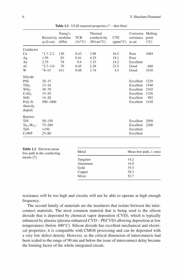
Ultra large-scale integration (ULSI) technology is one of the most dominant andimportant technologies of the 21st century. It is the base for the global electronicssystem industry.
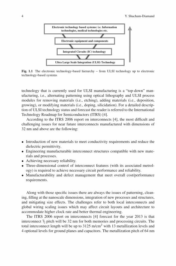
Our current information society is based on information technologies that havebeen developed in the last decade. Information technologies emerged as a resultof developments in silicon-based integrated circuits (ICs) that are the “engines”that collect, process, and distribute information (Fig. 1.1). The rapid developmentin highly complex hardware, allowing both digital and analog signal processing,conditioning, and dissemination, was accompanied by developments in softwareallowing better command and control of the hardware. All of this became possibledue to the invention of the integrated circuit, first on germanium (Kilby 1958) [1]and next on silicon (Noyce 1959) [1], and the rapid development toward ultra large-scale integration (ULSI) using complementary metal oxide semiconductor (silicon)(CMOS) technology.
The integration of few devices on chip was started as small-scale integration(SSI), followed by medium-scale integration (MSI), large-scale integration (LSI),very large-scale integration (VLSI), and finally ultra large-scale integration (ULSI).The integrated circuit includes transistors as the switching devices and interconnectsthat interface the switches between themselves and the external world. Typical inte-grated circuit (IC) dimensions are between few millimeters (length or width) andfew centimeters. It is laid on a thin (slightly less than 1 mm) single-crystal siliconwafer forming arrays of chips. The chips are separated by narrow scribing lanesthat define boundaries along them; the chips are later separated and packaged. Fora detailed description of the ULSI processing the reader is referred, for example, toreferences [2] and [3].
The term ULSI was coined when the critical dimension of the patterns withinthe micro-chips reached the range of 0.25 μm. Current ULSI circuits have fea-tures with dimensions in the nanoscale region (smaller than ∼100 nm). This reflectsthe transition from the era of micron-scale electronics into the nanoscale era. The
Y. Shacham-Diamand (B)School of EE, Tel Aviv University, Tel Aviv 69978, Israele-mail: [email protected]
3Y. Shacham-Diamand et al. (eds.), Advanced Nanoscale ULSI Interconnects:Fundamentals and Applications, DOI 10.1007/978-0-387-95868-2_1,C© Springer Science+Business Media, LLC 2009
4 Y. Shacham-Diamand
Ultra Large Scale Integration (ULSI) Technology
Integrated Circuits (IC) technology
Electronic equipment and components
Electronic technology based systems: i.e. Informationtechnologies, medical technologies etc.
Fig. 1.1 The electronic technology-based hierarchy – from ULSI technology up to electronictechnology-based systems
technology that is currently used for ULSI manufacturing is a “top-down” man-ufacturing, i.e., alternating patterning using optical lithography and ULSI processmodules for removing materials (i.e., etching), adding materials (i.e., deposition,growing), or modifying materials (i.e., doping, silicidation). For a detailed descrip-tion of ULSI technology status and forecast the reader is referred to the InternationalTechnology Roadmap for Semiconductors (ITRS) [4].
According to the ITRS 2006 report on interconnects [4], the most difficult andchallenging issues for near future interconnects manufactured with dimensions of32 nm and above are the following:
• Introduction of new materials to meet conductivity requirements and reduce thedielectric permittivity.
• Engineering manufacturable interconnect structures compatible with new mate-rials and processes.
• Achieving necessary reliability.• Three-dimensional control of interconnect features (with its associated metrol-
ogy) is required to achieve necessary circuit performance and reliability.• Manufacturability and defect management that meet overall cost/performance
requirements.
Along with those specific issues there are always the issues of patterning, clean-ing, filling at the nanoscale dimensions, integration of new processes and structures,and mitigating size effects. The challenges refer to both local interconnects andglobal wiring scaling issues which may affect circuit layouts and architecture toaccommodate higher clock rate and better thermal engineering.
The ITRS 2006 report on interconnects [4] forecast for the year 2013 is thatinterconnect 1/2 pitch will be 32 nm for both memories and processing circuits. Thetotal interconnect length will be up to 3125 m/cm2 with 13 metallization levels and4 optional levels for ground planes and capacitors. The metallization pitch of 64 nm
1 Challenges in ULSI Interconnects – Introduction to the Book 5
will be with Cu lines with aspect ratio of 1.9 (height/width) for micro processorunits (MPUs) that can carry a maximum current density of 8.08 × 10⁶ A/cm2. Thecontact aspect ratio is expected to be up to 20 for dynamic random access memories(DRAM) which have more regular and, hence, denser layouts than MPUs. The delayof such Cu lines depends on their length, their driving circuit, and the capacitive loadfor both their sides and at their end. For a 1 mm long line the delay of a minimumsize wire will be ∼3.45 ns assuming that the effective specific resistance of suchlines will be in the range of 4.83 μ�·cm.
Longer term forecast for the year 2020 assumes 28 nm pitch for the metalliza-tion, 14 metal layers, total interconnect length of 7243 m/cm2, aspect ratio of 2(height/width), maximum current density of 2.74 × 10⁷ A/cm2, and an RC delayfor a 1 mm long line of ∼23.4 ns, assuming that the effective specific resistance ofsuch lines will be in the range of 8.2 μ�·cm. Note that one of the key problems thatwill limit Cu interconnects in the far future is the rapid increase in the line-specificresistivity due to size-dependent scattering and the effect of barriers that reduces theeffective cross section of the Cu lines.
1.1 Material Issues in Cu Interconnects
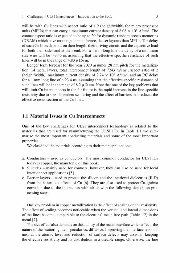
One of the key challenges for ULSI interconnect technology is related to thematerials that are used for manufacturing the ULSI ICs. In Table 1.1 we sum-marize the most important conducting materials and some of the most importantproperties.
We classified the materials according to their main applications:
a. Conductors – used as conductors. The most common conductor for ULSI ICstoday is copper, the main topic of this book.
b. Silicides – mainly used for contacts; however, they can also be used for localinterconnect applications [5].
c. Barrier layers – used to protect the silicon and the interlevel dielectrics (ILD)from the hazardous effects of Cu [6]. They are also used to protect Cu againstcorrosion due to the interaction with air or with the following deposition pro-cessing steps.
One key problem in copper metallization is the effect of scaling on the resistivity.The effect of scaling becomes noticeable when the vertical and lateral dimensionsof the lines become comparable to the electrons’ mean free path (Table 1.2) in themetal [7].
The size effect also depends on the quality of the metal interface which affects thenature of the scattering, i.e., specular vs. diffusive. Improving the interface smooth-ness at the atomic level and reduction of surface defects may assist in keepingthe effective resistivity and its distribution in a useable range. Otherwise, the line
6 Y. Shacham-Diamand
Table 1.1 ULSI material properties (∗ – thin film)
Resistivity(μ�·cm)
Young’smodulus(GPa)
TCR(%/◦C)
Thermalconductivity(W/cm/◦C)
CTE(ppm/◦C)
Corrosionresistancein air
Meltingpoint(◦C)
ConductorCu ∗1.7–2.2 130 0.43 3.98 16.5 Poor 1084Ag 1.59 83 0.41 4.25 19.1 PoorAu 2.35 78 0.4 3.15 14.2 ExcellentAl ∗2.7–3.0 70 0.45 2.38 23.5 Good 660W ∗8–15 411 0.48 1.74 4.5 Good 3410
SilicidePtSi 28–33 Excellent 1229TiSi2 13–16 Excellent 1540WSi2 30–70 Excellent 2165CoSi2 15–20 Excellent 1326NiSi 14–20 Excellent 992Poly Si(heavilydoped)
500–1000 Excellent 1410
BarriersTiN 50–150 Excellent 2950Ti0.3W0.7 75–200 Excellent 2200TaN >150 ExcellentCoWP 25–80 Excellent
Table 1.2 Electron meanfree path in the conductingmetals [7]
Metal Mean free path, λ (nm)
Tungsten 14.2Aluminum 14.9Gold 35.5Copper 39.3Silver 52.7
resistance will be too high and circuits will not be able to operate at high enoughfrequency.
The second family of materials are the insulators that isolate between the inter-connect materials. The most common material that is being used is the silicondioxide that is deposited by chemical vapor deposition (CVD), which is typicallyenhanced by plasma (plasma-enhanced CVD – PECVD) allowing deposition at lowtemperatures (below 400◦C). Silicon dioxide has excellent mechanical and electri-cal properties; it is compatible with CMOS processing and can be deposited witha very low defect density. However, as the critical dimension of interconnects hadbeen scaled to the range of 90 nm and below the issue of interconnect delay becamethe limiting factor of the whole integrated circuit.

1 Challenges in ULSI Interconnects – Introduction to the Book 7
1.2 Interconnect Performance Issues
Interconnect affects the performance of the circuit. Here is a short list of the mainperformance variables that characterize ULSI ICs:
• Speed – it depends on the delay due to the loading of the parasitic capacitancesof the lines and the series resistance of the conducting lines (interconnects) andthe switching devices. We refer to this as “RC delays.”
• Power dissipation – the dynamic power dissipation is proportional to the parasiticcapacitance, to the power supply squared, and to the clock frequency. There isalso some utilization factor that may take into consideration the average actualtransition rate between logical states per unit time, which is only a fraction of theclock frequency that describes the maximum possible transition rates betweenlogic states.
• Cost – interconnects define a significant part of the chip and they affect its area,thus the number of chips per wafer, and the wafer yield; both factors that affectcost. Interconnects also require many lithography and patterning steps that are asignificant factor of the overall cost of manufacturing.
• Defect density – there are many interconnect layers and each one has a largenumber of components. Therefore, significant number of defects, such as shortsand opens, are related to the interconnect process. It also definitely affects thecost of manufacturing.
Lowering the RC delay is possible by one of the following ways:
a. reducing the interconnect resistance – reducing the metal-specific resistance;b. reducing the parasitic capacitance – lowering the dielectric constant of the inter-
level dielectrics;c. optimizing the interconnect geometry – optimizing the aspect ratio, improved
layout on critical points;d. improved device properties – higher current-driving capabilities;e. improved circuit design – adding repeaters, use of transmission lines [8, 7].
Note that all of the above are a subset of the overall requirements which alsoinclude requirements for manufacturability, cost performance, and thermal manage-ment.
Reducing the interconnect resistance was achieved by the transition fromaluminum to copper metallization. Improving the copper-effective resistance isachieved by lowering its barrier layer thickness and improving its interface prop-erties. Lowering the parasitic capacitance is possible by using dielectric materi-als with a lower dielectric constant – low-k dielectrics. Intensive study of bothorganic and organic dielectrics with low dielectric constant has been under-way and it yields few interesting materials that are considered as candidatesto replace silicon dioxide. Low-k materials are classified as solid and porous
8 Y. Shacham-Diamand
materials, where the porous materials offer lower dielectric constant; however, theirporosity generates some major processing challenges.
The absolute value of resistance and capacitance is also determined by the lines’actual dimensions. Therefore, the overall interconnects’ layout plays an importantrole on the chip performance. Due to the high complexity of current ULSI chips,which may contain >108–109 devices and interconnects, it is difficult to simulatethe overall chip performance. Therefore, although there are current “known bestmethods” for layout the problem is far from being solved and there is a dire needfor better algorithms improving the layout and achieving better performance.
Improving the device properties has been achieved recently by the followingways:
a. Using bipolar devices with the CMOS circuits – this technology, known asBiCMOS, includes bipolar devices which have better current-driving capabil-ities than MOS transistors. It is used for driving high capacitive loads such aslong buses and interfacing pads.
b. The introduction of silicon on insulator technology – lowering the source/drainparasitic capacitances eliminates significance of the devices’ parasitic capaci-tance, therefore allowing better performance, i.e., higher speed at lower dissi-pated power.
c. The successful implementation of SiGe (Silicon–germanium) technologies.There are few possibilities that are being explored:
c.1. p-type MOS transistors with improved current-driving capabilities andc.2. strained silicon transistors where the conduction is in single crystal silicon
and the SiGe technology is used to apply the stress.
The last option improving interconnect performance is by improving the circuitdesign, for example, adding repeaters and choosing logic design with the least num-ber of transitions between stages for the given application if possible (for reviews ofon-chip interconnect the reader is referred to references [8, 7, 9]).
1.3 Interconnect Process Issues
A key development in modern ULSI manufacturing was the introduction of theDamascene process by P. Andricacos and his colleagues from IBM in 1998 [10].The transition from the old aluminum process, which uses negative lithography,to the new Cu process (see Fig. 1.2), using positive lithography, revolutionized theindustry.
Altogether Al-negative patterning was well established and yielded excellentresults; it was impossible to apply it to copper patterning because Cu has no volatilespecies in conventional plasma etch processes; therefore, it was impossible to useconventional photoresist-based lithography for Cu patterning. In addition to thisthe transition to deep lithography preferred planar surface since the depth of focus
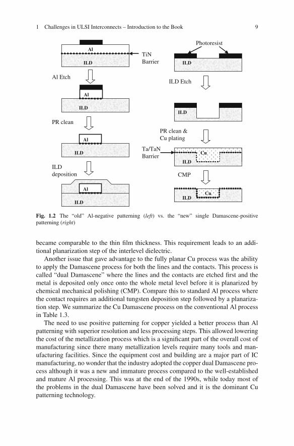
1 Challenges in ULSI Interconnects – Introduction to the Book 9
Al Etch
ILD
ILD
ILD
Al
Al
ILD
ILD
ILD
ILD
Cu
Cu
ILD Etch
PR clean &Cu plating
CMP
ILD
PR clean
ILDdeposition
TiNBarrier
Ta/TaNBarrier
Photoresist
Al
Al
Fig. 1.2 The “old” Al-negative patterning (left) vs. the “new” single Damascene-positivepatterning (right)
became comparable to the thin film thickness. This requirement leads to an addi-tional planarization step of the interlevel dielectric.
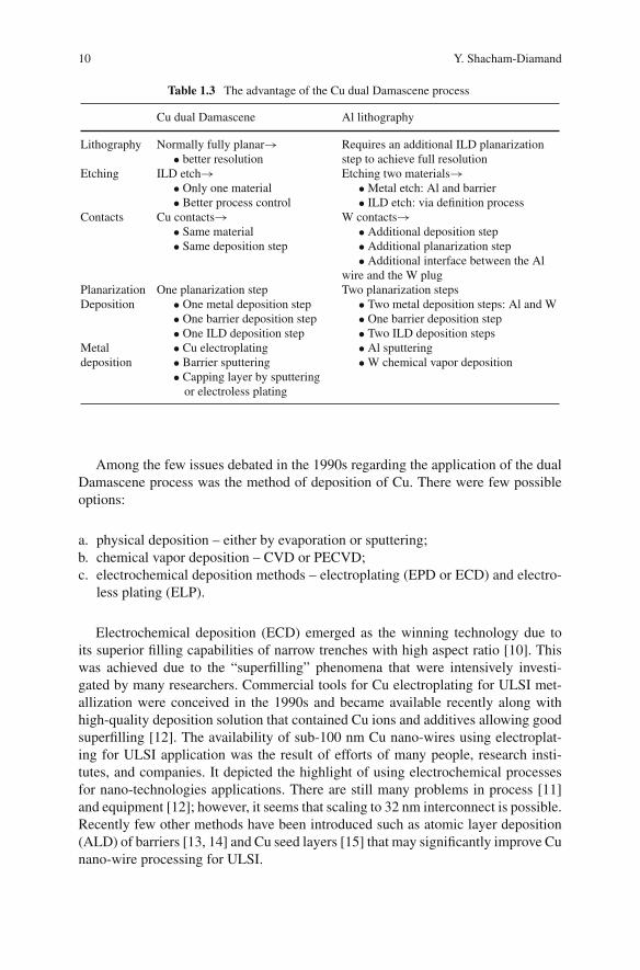
Another issue that gave advantage to the fully planar Cu process was the abilityto apply the Damascene process for both the lines and the contacts. This process iscalled “dual Damascene” where the lines and the contacts are etched first and themetal is deposited only once onto the whole metal level before it is planarized bychemical mechanical polishing (CMP). Compare this to standard Al process wherethe contact requires an additional tungsten deposition step followed by a planariza-tion step. We summarize the Cu Damascene process on the conventional Al processin Table 1.3.
The need to use positive patterning for copper yielded a better process than Alpatterning with superior resolution and less processing steps. This allowed loweringthe cost of the metallization process which is a significant part of the overall cost ofmanufacturing since there many metallization levels require many tools and man-ufacturing facilities. Since the equipment cost and building are a major part of ICmanufacturing, no wonder that the industry adopted the copper dual Damascene pro-cess although it was a new and immature process compared to the well-establishedand mature Al processing. This was at the end of the 1990s, while today most ofthe problems in the dual Damascene have been solved and it is the dominant Cupatterning technology.
10 Y. Shacham-Diamand
Table 1.3 The advantage of the Cu dual Damascene process
Cu dual Damascene Al lithography
Lithography Normally fully planar→• better resolution
Requires an additional ILD planarizationstep to achieve full resolution
Etching ILD etch→• Only one material• Better process control
Etching two materials→• Metal etch: Al and barrier• ILD etch: via definition process
Contacts Cu contacts→• Same material• Same deposition step
W contacts→• Additional deposition step• Additional planarization step• Additional interface between the Al
wire and the W plugPlanarization One planarization step Two planarization stepsDeposition • One metal deposition step
• One barrier deposition step• One ILD deposition step
• Two metal deposition steps: Al and W• One barrier deposition step• Two ILD deposition steps
Metaldeposition
• Cu electroplating• Barrier sputtering• Capping layer by sputtering
or electroless plating
• Al sputtering• W chemical vapor deposition
Among the few issues debated in the 1990s regarding the application of the dualDamascene process was the method of deposition of Cu. There were few possibleoptions:
a. physical deposition – either by evaporation or sputtering;b. chemical vapor deposition – CVD or PECVD;c. electrochemical deposition methods – electroplating (EPD or ECD) and electro-
less plating (ELP).
Electrochemical deposition (ECD) emerged as the winning technology due toits superior filling capabilities of narrow trenches with high aspect ratio [10]. Thiswas achieved due to the “superfilling” phenomena that were intensively investi-gated by many researchers. Commercial tools for Cu electroplating for ULSI met-allization were conceived in the 1990s and became available recently along withhigh-quality deposition solution that contained Cu ions and additives allowing goodsuperfilling [12]. The availability of sub-100 nm Cu nano-wires using electroplat-ing for ULSI application was the result of efforts of many people, research insti-tutes, and companies. It depicted the highlight of using electrochemical processesfor nano-technologies applications. There are still many problems in process [11]and equipment [12]; however, it seems that scaling to 32 nm interconnect is possible.Recently few other methods have been introduced such as atomic layer deposition(ALD) of barriers [13, 14] and Cu seed layers [15] that may significantly improve Cunano-wire processing for ULSI.
1 Challenges in ULSI Interconnects – Introduction to the Book 11
In this book we cover the latest issues in Cu nano interconnect technology forULSI applications. We focus on the electrochemical issues related to Cu nano-wiresapplications. In this book the issues that are briefly described in this introduction areoutlined one by one. While the majority of the Cu nano-technology issues are relatedto ULSI application, there are possible other applications. Therefore, we presentin the last chapter a brief review and forecast of some promising electrochemical-based nano-scale metallization schemes for various applications mostly related toelectronics.
References
1. Kilby, J. S.: Invention of the integrated circuit. IEEE Trans. Electron. Devices 23, 648 (1976)2. van Zant, P.: Microchip Fabrication: A Practical Guide to Semiconductor Processing. McGraw
Hill, New York (2000)3. Campbell, S. A.: The Science and Engineering of Microelectronic Fabrication. Oxford Uni-
versity Press, New York (2001)4. www.itrs.net5. Murarka, S. P.: Transition metal silicides. Ann. Rev. Mater. Sci. 13, 117 (1983)6. Shacham-Diamand, Y.: Barrier layers for Cu ULSI metallization. J. Electronic Mater. 30(4),
336–344 (2001)7. Davis, J. A.; Venkatesan, R.; Kaloyeros, A.; Beylansky, M.; Souri, S. J.; Banerjee, K.; Member
IEEE, Saraswat, K. C.; and Rahman A.: Interconnect limits on Gigascale Integration (GSI) Inthe 21st century. Proc. IEEE 89(3), (2001)
8. Havemann, R. H.; and Hutchby, J. A.: High-performance interconnects: An integrationoverview. Proc. IEEE 89(5), 586–601, (2001)
9. Edelstein, M. D.; Sai-Halasz, G. A.; and Mii, Y.-J.: LSl on-chip interconnection performancesimulations and measurements. IBM J. Res. & Dev. 39(4), 383–401 (1995)
10. Andricacos, P. C.; Uzoh, C.; Dukovic, J. O.; Horkans, J.; and Deligianni, H.: Damascenecopper electroplating for chip interconnections. IBM J. Res. & Dev. 12(5), 567–574 (1998)
11. Moffat, T. P.; Wheeler, D.; Edelstein, M. D.; and Josell, D.: Superconformal film growth:Mechanism and quantification. IBM J. Res. & Dev. 49(1), 19–36, (2005)
12. Ritzdorf, T. L.; Wilson, G. J.; McHugh, P. R.; Woodruff, D. J.; Hanson, K. M.; and Fulton, D.:Design and modeling of equipment used in electrochemical processes for microelectronics.IBM J. Res. & Dev. 49(1), 65–87, (2005)
13. Ritala, M.; Kalsi, P.; Riihela, D.; Kukli, K.; Leskela, M.; and Jokinen, J.: Controlled growthof TaN, Ta3N5, and TaOxNy thin films by atomic layer deposition. Chem. Mater. 11,1712 (1999)
14. Rossnagel, S. M.; Sherman, A.; and Turner, F.: Plasma-enhanced atomic layer deposition ofTa and Ti for interconnect diffusion barriers. J. Vac. Sci. and Technol. B18, 2016 (2000)
15. Pathangey, B. and Solanki, R.: Atomic layer deposition for nanoscale thin films. Vac. Technol.Coating 1, 32 (2000)
Part IITechnology Background
Part II presents the technological background for interconnect in ULSI systems.It includes detailed description of MOS device and interconnects scaling physics(Chapter 2). Chapter 3 is about electrical performance of Cu interconnects for ULSIapplications. It is well known that the steady growth in complexity of integratedelectronic systems requires a growing number of metal interconnect layers in ULSIchips. The role of interconnects in integrated electronic systems is described in thischapter: Metrics for evaluating the quality of signal interconnections are presented,and simple electrical circuit models for interconnects are introduced. In light ofthese models, the fundamental problem of interconnect scaling is presented anddesign approaches for addressing the problem are briefly surveyed. As there are lotsof deposition techniques, either electroless or electrodeposition, available elsewhereChapter 4 presented a brief description of electrodeposition process and a focuseddiscussion of copper electrodeposition for chip interconnects. It must be empha-sized that different chip manufacturers have their unique combination of electrode-position tools, proprietary tailored bath, and integration scheme for copper chipinterconnects. Successful implementation of the copper electrodeposition processin high-volume chip manufacturing involves equal attention to metrology, processintegration, and reliability issues. Besides void-free deposition of interconnect struc-tures, selection of a reliable CMP process, excellent adherence of copper lines/viasto the dielectric, low resistivity, and resistance to electromigration are some of thekey requirements for a high-yielding, reliable interconnect electrodeposition pro-cess. All these aspects are addressed in greater detail in different chapters of thisbook. Along with this Chapter 5, “Electrophorectic Deposition,” defined the pro-cess of electrophoretic depositionand the process is summarized. The limitationsof the process are explained and potential applications in the microelectronics sec-tor are identified. Three areas in which industrial feasibility has been explored arethen described in more detail. In addition to deposition technologies, proper deviceintegration technology is important. As wafer-level 3D integration (i.e., 3D stack-ing prior to singulation of wafers into individual chips) has become an increasinglyactive research topic, without any large-scale IC manufacturing, Chapter 6 “WaferLevel 3D Integration for ULSI Interconnects” presents types of 3D integration,BEOL-based wafer-level 3D processing and wafer-level 3D design opportunities.Wafer-level interconnectivity is extended to multiple device levels.
Chapter 2MOS Device and Interconnects Scaling Physics
Marc Van Rossum
2.1 Device Fundamentals
2.1.1 The MOSFET Transistor
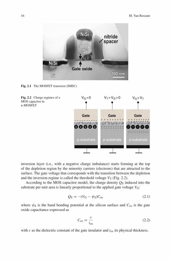
2.1.1.1 Basic Device Physics
The metal-oxide-semiconductor field-effect transistor (MOSFET) is the mostcommon active device in today’s integrated circuits. Its basic structure consists of adoped silicon well, with at the opposite ends two highly doped contact regions (thesource and drain junctions) allowing the current to pass close to the well surface(Fig. 2.1). In an n-type MOSFET, the well region is p-type doped and the sourceand drain are n+ doped, whereas the reverse polarity scheme applies for p-typedevices. CMOS circuits contain both n-MOS and p-MOS transistors combined toform various logic gates. The transistor body is electrically isolated from the sur-rounding circuitry by a thick “field” oxide. A third electrode (the gate), to whichthe input signal is applied, is sitting on top of the well. It consists of an electricalcontact layer (usually heavily doped polysilicon with a metallic top layer) separatedfrom the silicon substrate by a thin insulator film made of thermally grown silicondioxide. The substrate is thus capacitively coupled to the gate electrode, making theMOSFET a nearly ideal switch element due to the high isolation between input andoutput.
The output signal modulation takes place by varying the potential of the gatewith respect to the substrate, which affects the charging of the MOS capacitor. Inan n-MOSFET for instance, a negative gate voltage induces a positive (hole) chargeaccumulation region under the gate insulator. At positive gate voltages, holes arerepelled into the substrate, creating a depletion region with fixed negative chargesdue to the ionized acceptor ions. At even more positive voltages, a negative charge
M.V. Rossum (B)IMEC, Kapeldreef 75, B-3001, Leuven, Belgiume-mail: [email protected]
15Y. Shacham-Diamand et al. (eds.), Advanced Nanoscale ULSI Interconnects:Fundamentals and Applications, DOI 10.1007/978-0-387-95868-2_2,C© Springer Science+Business Media, LLC 2009
16 M. Van Rossum
Gate oxide
Fig. 2.1 The MOSFET transistor (IMEC)
Gate
p-substrate
Gate
p-substrate
+ + + + + + + + +– – – – – – – – – –
– – – – – – – – – – – – – – – – – – – – + + + + +
Gate
p-substrate
+ + + + + + + + +
– – – – – – – – – – – – – – – – – – – –
+ + + + + + + + +
VG < 0 VT > VG > 0 VG > VTFig. 2.2 Charge regimes of aMOS capacitor inn-MOSFET
inversion layer (i.e., with a negative charge imbalance) starts forming at the topof the depletion region by the minority carriers (electrons) that are attracted to thesurface. The gate voltage that corresponds with the transition between the depletionand the inversion regime is called the threshold voltage VT (Fig. 2.2).
According to the MOS capacitor model, the charge density QS induced into thesubstrate per unit area is linearly proportional to the applied gate voltage VG:
QS = −(VG − ψS)Cox (2.1)
where ψS is the band bending potential at the silicon surface and Cox is the gateoxide capacitance expressed as
Cox = ε
tox(2.2)
with ε as the dielectric constant of the gate insulator and tox its physical thickness.


![[C. Y. Chang, Simon M. Sze] ULSI Devices(BookFi.org)](https://static.fdocuments.net/doc/165x107/55cf9409550346f57b9f371b/c-y-chang-simon-m-sze-ulsi-devicesbookfiorg.jpg)


