Advanced MOSFET Designs and Implications for … Abstract Advanced MOSFET Designs and Implications...
110
Advanced MOSFET Designs and Implications for SRAM Scaling Changhwan Shin Tsu-Jae King Liu, Ed. Borivoje Nikolic, Ed. Eugene Haller, Ed. Electrical Engineering and Computer Sciences University of California at Berkeley Technical Report No. UCB/EECS-2012-50 http://www.eecs.berkeley.edu/Pubs/TechRpts/2012/EECS-2012-50.html May 1, 2012
Transcript of Advanced MOSFET Designs and Implications for … Abstract Advanced MOSFET Designs and Implications...

Advanced MOSFET Designs and Implications for
SRAM Scaling
Changhwan ShinTsu-Jae King Liu, Ed.Borivoje Nikolic, Ed.Eugene Haller, Ed.
Electrical Engineering and Computer SciencesUniversity of California at Berkeley
Technical Report No. UCB/EECS-2012-50
http://www.eecs.berkeley.edu/Pubs/TechRpts/2012/EECS-2012-50.html
May 1, 2012

Copyright © 2012, by the author(s).All rights reserved.
Permission to make digital or hard copies of all or part of this work forpersonal or classroom use is granted without fee provided that copies arenot made or distributed for profit or commercial advantage and that copiesbear this notice and the full citation on the first page. To copy otherwise, torepublish, to post on servers or to redistribute to lists, requires prior specificpermission.

Advanced MOSFET Designs and Implications for SRAM Scaling
By
Changhwan Shin
A dissertation submitted in partial satisfaction of the
requirements for the degree of
Doctor of Philosophy
in
Engineering - Electrical Engineering and Computer Sciences
in the
Graduate Division
of the
University of California, Berkeley
Committee in charge:
Professor Tsu-Jae King Liu, Chair Professor Borivoje Nikolić Professor Eugene E. Haller
Spring 2011

Advanced MOSFET Designs and Implications for SRAM Scaling
Copyright © 2011
by
Changhwan Shin

1
Abstract
Advanced MOSFET Designs and Implications for SRAM Scaling
by
Changhwan Shin
Doctor of Philosophy in Engineering – Electrical Engineering and Computer Sciences
University of California, Berkeley
Professor Tsu-Jae King Liu, Chair
Continued planar bulk MOSFET scaling is becoming increasingly difficult due to increased random variation in transistor performance with decreasing gate length, and thereby scaling of SRAM using minimum-size transistors is further challenging. This dissertation will discuss various advanced MOSFET designs and their benefits for extending density and voltage scaling of static memory (SRAM) arrays. Using three-dimensional (3-D) process and design simulations, transistor designs are optimized. Then, using an analytical compact model calibrated to the simulated transistor current-vs.-voltage characteristics, the performance and yield of six-transistor (6-T) SRAM cells are estimated. For a given cell area, fully depleted silicon-on-insulator (FD-SOI) MOSFET technology is projected to provide for significantly improved yield across a wide range of operating voltages, as compared with conventional planar bulk CMOS technology. Quasi-Planar (QP) bulk silicon MOSFETs are a lower-cost alternative and also can provide for improved SRAM yield. A more printable "notchless" QP bulk SRAM cell layout is proposed to reduce lithographic variations, and is projected to achieve six-sigma yield (required for terabit-scale SRAM arrays) with a minimum operating voltage below 1 Volt.
___________________________________ Professor Tsu-Jae King Liu, Chair Dissertation Committee Chair

i
To my parents for their unbounded love and support, to my brother for his sincere encouragement,
and to my wife for her devoted love.

ii
Contents Table of Contents ii List of Figures viii List of Tables x Acknowledgements xi
Table of Contents Chapter 1: Introduction ………………………......………..……………1
1.1 Static Random Access Memory (SRAM) ………………………………………..1
1.1.1 SRAM Basics ……………………………………………………………...1
1.1.2 Alternative SRAM Cell Architectures …………………………………….3
1.1.3 Sources of VT Variation ……………………………..…………………….5
1.1.3.1 Random Dopant Fluctuations (RDF) ……………………………..6
1.1.3.2 Gate Length Fluctuations …………………………………………7
1.1.3.3 Gate Work-Function Variation (WFV) …………………………...8
1.1.4 Approaches to Mitigating the Impact of VT Variation for SRAM ..…….....8

iii
1.2 Advanced Transistor Designs for the 22nm Node and Beyond ……………….…9
1.2.1 Planar Silicon-on-Insulator (SOI) MOSFETs .…………………………….9
1.2.1.1 Partially-depleted SOI (PD-SOI) MOSFET .………….………….9
1.2.1.2 fully-depleted SOI (FD-SOI) MOSFET .......………….………...10
1.2.2 Multiple-Gate MOSFETs .………………………………………………..12
1.2.2.1 Double-Gate FinFET and SOI Tri-Gate MOSFETs …………..12
1.2.2.2 Gate-All-Around (GAA) MOSFET ………………….………..13
1.3 Research Objectives and Thesis Overview …………………………………..…14
1.4 References …………………………………………………….………………...15
Chapter 2: Performance and Area Scaling Benefits of FD-SOI Technology for 6-T SRAM Cells at the 22nm node …......23
2.1 Introduction ………………………………..……………………………………23
2.2 Thin-BOX FD-SOI Technology ……………………………………………......23
2.2.1 MOSFET Design Optimization …………………………………………..23
2.2.2 Impact of Random Variations ……………………………………………27
2.3 6-T SRAM Cell Performance Comparison …………………………………......28
2.3.1 Nominal Cell Design ……………………………………………………..28

iv
2.3.2 Dependency of SRAM Performance Metrics on Cell Ratio, Pull-Up Ratio, and VDD ………………………………………………………………………30
2.4 Yield-Aware SRAM Cell Design …………………………………....................31
2.4.1 Iso-Area Comparison ...…………………………………………………..32
2.4.2 Iso-Yield Comparison ...………………………………………………….33
2.4.3 Minimum Operating Voltage (Vmin) for read and write operation ....…….33
2.5 Summary ………………………..…………………………………....................34
2.6 References ………………………………….......................................................35
2.A Appendix .………………………………….......................................................37
Chapter 3: Study of Random Dopant Fluctuation (RDF) Effects for the Quasi-Planar Bulk MOSFET ……………..……...38
3.1 Introduction ………………………………..……………………………………38
3.2 Device Simulation Approach ….……………………………………………......39
3.2.1 Nominal Bulk MOSFET Designs ………………………………………..39
3.2.2 Methodology for Atomistic Device Simulation ………………………….39
3.3 Results and Discussion ….……………………………………………................42
3.3.1 Planar vs. Quasi-Planar Bulk MOSFET Designs ………………………...42
3.3.2 Body RDF vs. Source/Drain RDF …………….………………………….43

v
3.3.3 Assessment of VTH Adjustment Approaches …………………………….43
3.4 Summary ….…………………………………………….....................................45
3.5 References ….……………………………………………...................................45
Chapter 4: Full three-dimensional Simulation of 6-T SRAM Cells for the 22nm node …………………...……………..……...47
4.1 Introduction ………………………………..……………………………………47
4.2 Segmented Bulk MOSFET Structure and Fabrication Process ….……………...49
4.3 6-T SRAM Cell Designs ….………………………………………………….....49
4.4 Global and Local Variation Analysis ….………………………………………..52
4.5 Simulation of Single-Event-Upset …….………………………………………..53
4.6 Summary …….………………………………………………………………….55
4.7 References ……………………….…….………………………………………..55
Chapter 5: Quasi-Planar Bulk CMOS Technology for Improved SRAM Scalability …………..……..............58
5.1 Introduction ………………………………..……………………………………58
5.2 Device Fabrication ….……………......................................................................59
5.3 Results and Discussion ….……………................................................................61

vi
5.3.1 Quasi-Planar vs. Planar MOSFETs ………………………..……………..61
5.3.1.1 Improved Performance …………………………………………..61
5.3.1.2 Suppressed VTH Variation ……………………………………….62
5.3.1.3 Improved Short-Channel Effect …………………………………64
5.3.1.4 Increased Narrow Width Effect …………………………………65
5.3.1.5 Compact Transistor Model …..………………………………….65
5.3.1.4 Increased Narrow Width Effect …………………………………65
5.3.2 Benefits of Quasi-Planar Bulk CMOS Technology for 6-T SRAM ………67
5.3.2.1 Cell Yield Enhancement ………………………………………...67
5.3.2.2 Supply-Voltage Reduction ……………….……………………...67
5.3.1.2 Suppressed VTH Variation ……………………………………….62
5.4 Summary …….………………………………………………………………….68
5.5 References ……………………….…….………………………………………..69
Chapter 6: Performance and Yield Benefits of Quasi-Planar Bulk CMOS Technology for 6-T SRAM at the 22 nm Node ………….71
6.1 Introduction ………………………………..……………………………………71
6.2 Quasi-Planar Bulk Technology ….……………...................................................73
6.2.1 Optimized MOSFET Performance ………………………..……….73

vii
6.2.2 Impact of Random and Systematic Variations …………………….75
6.3 Notchless 6-T SRAM Cell Designs ….……………............................................77
6.4 SRAM Yield Estimation ….…………….............................................................81
6.4.1 Iso-Area and Iso-Yield Comparisons
between Planar and Quasi-Planar Bulk Cell Designs …………….81
6.4.2 Notchless Quasi-Planar Bulk SRAM Cell Yield …………………82
6.5 Summary …….………………………………………………………………….83
6.6 References ……………………….…….………………………………………..83
Chapter 7: Conclusion ……………………………………….…………87
7.1 Contribution of This Work ………………………………..…………………….87
7.2 Suggested Future Work ….……………...............................................................90
A. Improved Manufacturability ………………..………..……….91
B. Independent Biasing Transistors ………………………..……92
C. Compatibility with Advanced Device Architecture ………….92
7.3 References ……………………….…….………………………………………..93

viii
List of Figures 1.1 Circuit schematic for a six-transistor (6-T) SRAM cell 2 1.2 Definition of the static noise margin and write-ability current 3 1.3 Alternative SRAM bit-cell architecture 4 1.4 Standard deviation of threshold voltage vs. channel length 5 1.5 Randomly distributed dopant atoms in an n-channel MOSFET 6 1.6 Illustration of a nano-scale MOSFET showing line-edge-roughness 7 1.7 Illustration of hypothetical metal gate film 8 1.8 Transmission electron micrograph image of a PD-SOI n-MOSFET with HK/MG 9 1.9 Product design compromises for planar bulk, PD-SOI, and FD-SOI 10 1.10 Experimental data for SOI layer thickness variation 11 1.11 FD-SOI technology features 12 1.12 Transmission electron micrograph image of FinFET structures 13 1.13 Transmission electron micrograph image of Omega-/Tri-gate MOSFET structures 13 1.14 Transmission electron micrograph image of twin silicon nanowire MOSFET 14
2.1a Cross-sectional view of a thin-BOX FD-SOI MOSFET structure 24 2.1b Experimental data for SOI thickness variation 25 2.2 Transfer characteristics of planar bulk and FD-SOI MOSFETs 26 2.3 Simulated I-V curves of pull-down transistor for LER/RDF 26 2.4 Comparisons of SNM and write current 29 2.5 Comparison of SRAM cell performance metrics 30 2.6 Impact of VDD scaling on 6-T SRAM cell performance metrics 31 2.7 Yield of Iw vs. Yield of SNM for FD-SOI and planar bulk 32 2.8 Yield of Iw vs. Yield of SNM for FD-SOI and enlarged planar bulk 33 2.9 Dependence of yield on VDD 34
3.1 3D bird-eye view and cross-sectional view of the quasi-planar bulk MOSFET 39 3.2 Example of a QP bulk MOSFET with atomistic doping profiles and isometric view 40 3.3 Simulated I-V curves for planar and QP bulk MOSFETs with atomistic doping 41 3.4 Comparison of body RDF vs. source/drain RDF effects 43 3.5 Impact of nominal VTH adjustment on VTH variation 44
4.1a Cross-sectional views of a two-striped SegFET 48 4.1b Front-end-of-line fabrication process steps for a SegFET 48

ix
4.2 6T-SRAM cell area scaling trend 49 4.3 3D 6-T SRAM cells simulation results 50 4.4 3D 6T-SRAM cell structures with fine meshing 51 4.5 SNM and Iw vs. VDD 52 4.6 SegFET vs. planar MOSFET comparison 53 4.7 Heavy ion beam modeling 54 4.8 Transient simulations of heavy-ion-beam strike on the high storage node 54
5.1 Sequence of front-end-of-line CMOS fabrication process steps for QP MOSFET 60 5.2a 0.149μm2 SRAM cell plan-view CDSEM image after gate patterning 60 5.2b XTEM taken along a poly-Si gate electrode in an SRAM array 60 5.3 Comparison of ON/OFF current statistics for planar vs. QP MOSFETs 61-62 5.4 Comparison of saturation VTH statistics for planar vs. QP MOSFETs 63 5.5 Pelgrom plots for NMOS and PMOS logic devices 64 5.6 Saturation threshold voltage with decreasing gate length 64 5.7 Measured reverse narrow width effect for devices with 36nm gate length 65 5.8 Comparison of measured and modeled output characteristics 66 5.9 Sigma and 3-sigma/median values for SNM and WRM 67 5.10 Degradation in 3-sigma/median for SNM and WRM 68 6.1 Bird-eye view of a quasi-planar bulk MOSFET and along/across the channel 72 6.2 Simulated transfer characteristics for planar and quasi-planar bulk MOSFETs 73 6.3 Simulated VTH,SAT for planar bulk vs. quasi-planar bulk MOSFETs 76 6.4 Half-bit cell layouts for notched and notchless SRAM cell designs 78 6.5 3-D 6-T SRAM cell simulation results 79 6.6a SRAM cell read current 80 6.6b PD device gate capacitance 80 6.6c Pseudo-transient simulation of the storage-node voltage during a write operation 80 6.7 SRAM cell sigma comparisons for SNM and IW 82 6.8 SRAM cell sigma comparisons for SNM and IW 82 7.1a Proposed new layout of the 6-T SRAM bit-cell 91 7.1b Circuit schematic of the 6-T SRAM bit-cell with external voltage skews 91 7.2 Conventional layout of a 6-T SRAM bit-cell 92

x
List of Tables 2.1 Optimized thin-BOX FD-SOI and Planar bulk MOSFET design parameters 25 2.2 Comparison of device performance parameters for VDD = 0.9 V 26 2.3 FD-SOI 6-T SRAM cell dimensions 29 2.4 Summary of SRAM cell performance metrics 34
4.1 SegFET 6T-SRAM cell dimensions for the 22nm node 50 6.1 Summary of transistor performance parameters 74 6.2 22nm-node 6-T SRAM cell layout parameters 79 6.3 Comparison of projected performance metrics and cell areas 81 7.1 Comparison of three different device architectures 90

xi
Acknowledgements During my time at Berkeley, lots of people have sincerely guided my research. I would like to begin by appreciating all of their kind help. In fact, I could not write this page without expressing my deepest thanks to my academic advisor, Professor Tsu-Jae King Liu, who is the epitome of a great mentor and guided me from unsure beginning as a fresh researcher to the bleeding-edge in my field of study. She has always been cordial, attentive, available and supportive throughout all the peaks and valleys of my Ph.D. course. In all research meeting, she never failed to advise me with her inspiring perspective, amazing engineering-intuition, tireless enthusiasm, and firm and solid knowledge. There is much about her management style that I would like to bring with me as I go into industry and/or academia. I am grateful for all the support and advice of Professor Borivoje Nikolić, chairing my qualifying examination and serving as a member of my dissertation committee. His keen perspective on SRAM was exceptionally helpful, and his sincere advice on leading my research opportunities toward a very meaningful contribution to device and circuit co-optimization was tremendously valuable. I also thank Professor Eugene E. Haller for serving on both my qualifying examination committee and my dissertation committee, and thank Professor Sayeef Salahuddin for serving my qualifying examination committee. Dr. Yasumasa Tsukamoto, former visiting scholar, provided invaluable guidance on SRAM designs, for which I am greatly grateful. His firm and rigorous SRAM knowledge has provided a great advantage toward understanding SRAM and all its tradeoffs. His experience in industry was also helpful for my research and future career. I hope to be as informative and impactful with my future colleagues as he is with his. Dr. Si-woo Lee, another former visiting scholar, became my wise counselor for both my research and life. While he was staying at Berkeley, I learned something new from him every day. I would like to thank several former and current students with regards to this work. With Dr. Andrew Carlson, Dr. Xin Sun, Min Hee Cho, and Nattapol Damrongplasit, I could establish the foundation of my research. They provided kind assistance and several helpful discussions on SRAM, advanced device structures, and their variability. With Dr. Zheng Guo, Seng Oon Toh, Aikaterini Papadopoulou, and Jaehwa Kwak, I had a lot of discussions on SRAM in test chips. They also kindly assisted with the logistics of tapeout and testing.

xii
In addition to the above, several others have provided indirect assistance. Dr. Donovan Lee and Dr. Joanna Lai helped me, among many other things, to acquire an American English language and to adapt myself to new circumstances at Berkeley. Jemin Park and Kanghoon Jeon sincerely helped me in times of need. Prof. Man Young Sung, Prof. Suki Kim, Prof. Soo-Won Kim, Prof. Tae-Geun Kim, Prof. Sang Bin Lee, Prof. Jae-Sung Rieh, Prof. Tae-Woong Yoon, Prof. James Jungho Pak, Prof. Woo-Young Choi, Prof. Songhwai Oh, Prof. Hyuck Choo, Dr. Vidya Varadarajan, Dr. Alvaro Padilla, Dr. Reinaldo Vega, Dr. Hei Kam, Dr. Louis Hutin, Dr. Jiwoong Lee, Dr. Daekyeong Moon, Dr. Jaein Jeong, Dr. Chuck Choongyeun Cho, Dr. Kihoon Kim, Dr. Gregory Freeman, Dr. Dae-kyu Park, Jason Cheng, Rhesa Nathanael, Zachery Jacobson, Wookhyun Kwon, Jaeseok “Jay” Jeon, Sung Hwan Kim, Byron Ho, Nuo Xu, Peter Matheu, Eung Seok Park, I-Ru “Tim” Chen, Yenhao “Philip” Chen, Jack Yaung, Sriramkumar V., Darsen D. Lu, Stan Baek, Ji-Hoon Park, Namseog Kim, Jung-Dong Park, Kwangmo Jung, Tae Joon Seok, Se Yong Park, Changho Suh, Kyoohyun Noh, Sunyoung Lee, Hyojin Kim, Hyerin Lee, Kangwook Lee, Sangyoon Han, Youngki Yoon, Shinwon Kang, Hongki Kang, Jaewon Jang, Chang-Seo Park, Yunsup Lee, Hyun Oh Song have also provided technical, educational, personal assistance in some form. I appreciate all of their help. This work has been funded through a few sources. First of all, my financial stability for my Ph.D. work came from the Korea Foundation of Advanced Studies (KFAS) Fellowship. This work was also supported in part by the Center for Circuit & System Solutions (C2S2) Focus Center, which is one of five research centers funded under the Focus Center Research Program (a Semiconductor Research Corporation program). In addition, fabrication of a 28nm test chip for studying 28nm quasi-planar bulk technology and data for FD-SOI wafer was donated by UMC (Dr. Cheng-Tzung Tsai and all the other UMC engineers involved to the 28nm test chip) and Soitec (especially, Dr. Carlos Mazuré and Mrs. Bich-Yen Nguyen), respectively. I would like to express my sincere gratitude for the financial and technical supports, and I will not forget to contribute back to them in future. Finally, I would not be here today were it not for my family. I can not thank my parents and my younger brother enough for their unbounded love and sacrifices. Their love will always hold a special place in my heart. Lastly, but most certainly not least, I would like to thank my wife, Yun Jeong Hwang, for her devoted love. She is my light at the end of the long tunnel, and I appreciate her.

1
Chapter 1
Introduction Improvement in integrated circuit (IC) performance and cost has been achieved largely by transistor scaling (i.e., minimum feature size reduction by a factor of 0.7 in every new technology node, or every 2 years) according to Moore’s Law [1, 2]. The resultant exponential growth in device count per chip has been led by the miniaturization of the static-random-access-memory (SRAM) bit-cell. Increasing process-induced variations in transistor performance with miniaturization down to the 22 nm technology node and beyond is a major technical challenge for continued advancement of planar-bulk/partially-depleted silicon-on-insulator (PD-SOI) complementary metal-oxide-semiconductor (CMOS) technology [3, 4]. In particular, continued SRAM cell-area scaling for increased storage density, reduction in operating voltage (VDD) for lower stand-by power consumption, and enhanced yield necessary to realize larger-capacity SRAM arrays (i.e., embedded level-2 or level-3 cache memory for microprocessor) become increasingly difficult to achieve. This thesis explores the benefits of advanced transistor structures and bit-cell design co-optimization for continued SRAM scaling.
1.1 Static Random Access Memory (SRAM)
1.1.1 SRAM Basics The SRAM cell incorporates a static latch, comprising two cross-coupled inverters, so that it does not require periodic refreshing to retain the stored information, provided that there is adequate power supply voltage for the cell (VDD,cell).

2
Figure 1.1. Circuit schematic for a six-transistor (6-T) SRAM cell, the most commonly used SRAM bit-cell architecture.
Fig. 1.1 shows the most commonly used SRAM bit-cell architecture, that is the six-transistor (6-T) SRAM cell. It consists of two cross-coupled inverters (PMOS pull-up transistors PUL and PUR and NMOS pull-down transistors PDL and PDR) and two access transistors (NMOS pass-gate transistors PGL and PGR). When the horizontally-running word-line (WL) is enabled (i.e., a row is selected in an array), the access transistors are turned on, and connect the storage nodes to the vertically-running bit-lines (BL and BL). In other words, they allow access to the cell for read and write operations, acting as bi-directional transmission gates.
The 6-T SRAM cell operates as follows: (1) For a read operation, the bit-lines are usually pre-charged to a high level (VDD) and then the word-line is selected (pulsed to a high level). On the side of the cell storing a logical ‘0’ (i.e., a low voltage), the bit-line is discharged via the pass-gate transistor and pull-down transistor, so that a differential voltage develops between the bit-lines. This differential voltage should be large enough for a sense amplifier to detect the state of the cell. The differential voltage should not be too large, however; otherwise the cross-coupled inverters could flip their state. (The read operation should be non-destructive.) The cell beta ratio, which is the ratio of the strength (drive current) of the pull-down transistor to that of the pass-gate transistor, should be sufficiently large to ensure that such a read disturbance does not occur. (2) For a write operation, the bit-lines are driven to complementary voltage levels via a write driver and then the word-line is selected. On the side of the cell for which the bit-line voltage is logical ‘0’ (i.e., a low voltage), the internal storage node is discharged through the pass-gate transistor. The cross-coupled inverters raise the voltage on the opposite storage node and latch the cell. The discharging strength of the pass-gate transistor must overcome the restoring strength of the pull-up transistor. The cell gamma ratio, which is the ratio of the strength of the pass-gate transistor to that of the pull-up transistor, should be sufficiently large to ensure that write failure does not occur.
PGL
PUL
PDL
QL
QR
BL BLWL
PDR
PUR
PGR
VDD,cell
GND
PGL
PUL
PDL
QL
QR
BL BLWL
PDR
PUR
PGR
VDD,cell
GND

3
Figure 1.2. (a) Definition of the static noise margin (SNM) from the read voltage transfer characteristics (VTC), or “butterfly curves” for a 6-T SRAM cell. The inset shows the biasing conditions for read operation. (b) Definition of the write-ability current from the write “N-curve.” The inset shows the biasing conditions for write operation. Note that the storage node QL is at logical ‘0’ voltage level.
Since Seevinck’s seminal work [5] in 1987, the most common metric for SRAM read stability is the read static noise margin (SNM), illustrated in Fig. 1.2(a). SNM is the maximum tolerable DC noise voltage at a storage node that does not cause a read disturbance, and it is the length of the side of the largest square that can fit into the “eyes” of the butterfly curves, i.e., the read voltage transfer characteristics (VTC), for the SRAM cell. The other metric for read stability utilizes the read N-curve [6, 7], which is measured by sweeping the voltage at the storage node QL (or QR) via the bit-line, with the word-line and two bit-lines biased at VDD, and monitoring the current sourced into the storage node. The write N-curve illustrated in Fig. 1.2(b) is obtained by sweeping the voltage at the storage node QR (QL), with BL (BL) and WL biased at VDD and BL (BL) biased at GND, and monitoring the current sourced into the storage node. The write-ability current [8, 9], Iw, is defined as the minimum current past the inverter PUL-PDL trip point, and is a measure of the difference between PGR and PUR currents.
1.1.2 Alternative SRAM Cell Architectures As explained in the previous section, the transistors within a 6-T SRAM cell must be sized properly (since drive current is proportional to transistor width) for the cell to meet both read and write margin specifications to guarantee proper operation. There is a fundamental tradeoff, therefore, between cell yield and cell layout area (i.e., cost). This tradeoff is worsened by the need to include design margin for process-induced variations in transistor threshold voltage (VT) since drive current is a function of VDD – VT.
Iw
0.0 0.2 0.4 0.6 0.8 1.00
20μ
40μ
60μ
80μ
100μ
I QR(A
)
VQR
(V)
Iw
0.0 0.2 0.4 0.6 0.8 1.00
20μ
40μ
60μ
80μ
100μ
I QR(A
)
VQR
(V)0.0 0.2 0.4 0.6 0.8 1.0
0.0
0.2
0.4
0.6
0.8
1.0
V Q
R
(V)
VQL
(V)
SNM
0.0 0.2 0.4 0.6 0.8 1.00.0
0.2
0.4
0.6
0.8
1.0
V Q
R
(V)
VQL
(V)
SNM PGL
PUL
PDL
QL
QR
BL BL
PDR
PUR
PGR
VDD,cell
GND
PGL
PUL
PDL
QL
QR
BL BL
PDR
PUR
PGR
VDD,cell
GND
(a) (b)
PGL
PUL
PDL
QL
QR
BLBL
PDR
PUR
PGR
VDD,cell
GND
PGL
PUL
PDL
QL
QR
BLBL
PDR
PUR
PGR
VDD,cell
GND

4
Figure 1.3. Alternative SRAM bit-cell architectures: (a) 4-T SRAM cell, (b) 7-T SRAM cell, (c) 8-T SRAM cell, and (d) 10-T SRAM cell.
Various alternative SRAM bit-cell architectures have been proposed to reduce cell area or to decouple the requirements for read stability and write-ability. The 4-T SRAM cell (Fig. 1.3(a)) consists of two PMOS pass-gate transistors and two NMOS pull-down transistors, resulting in relatively smaller cell area than the 6-T SRAM design [10-15]. It
WBL RBLWWLVDD,cell
GND
RWL
GND
/WL
WBL RBLWWLVDD,cell
GND
RWL
GND
/WL
(a) (b)
BL BLWL
GND
BL BLWL
GND
(c)
(d)
WBL WBLWWL
VDD,cell
GND
RWLRBL
GND
WBL WBLWWL
VDD,cell
GND
RWLRBL
GND
BL BLWWL
VDD,cell
GND
RWL
BL BLWWL
VDD,cell
GND
RWL

5
maintains a logical ‘1’ state at one of the internal storage nodes via PMOS transistor off-state leakage current. This results not only in higher static power consumption but also in larger susceptibility to VT variation (since transistor off-state leakage current varies exponentially with VT), so that the 4-T SRAM cell architecture is not promising for sub-22 nm SRAM technologies. The 7-T SRAM cell (Fig. 1.3(b)) [16] utilizes dedicated word-lines and bit-lines for read vs. write operations to avoid the possibility of a read disturbance even if the read SNM is lower than 0, so that minimum-width transistors can be used for minimal cell area. Takeda et al. [17] demonstrated 23% area-savings for a layout-optimized 7-T SRAM array (vs. a 6-T SRAM array), for the same operating speed. However, it has complexity in layout. The 8-T SRAM cell (Fig. 1.3(c)) [18-21] also utilizes dedicated word-lines and bit-lines for read vs. write operations, but uses complementary bit-lines for write operation as does a 6-T SRAM cell. Write disturbance is still a general issue for these alternative cell architectures. The 10-T SRAM cell (Fig. 1.3(d)) [22] decouples the storage nodes from the bit-lines to improve read stability, but requires the use of peripheral write-assist circuitry. These alternative SRAM cell architectures each have undesirable tradeoffs in cell area or performance as compared to the 6-T SRAM cell. This thesis therefore focuses on technological approaches to improve the scalability of the 6-T SRAM cell.
1.1.3 Sources of VT Variation VT variation is caused by two types of sources: systematic and random. Systematic sources include lithography-induced variations in channel length and width, which are deterministic and predictable. Random sources include as gate line-edge-roughness (LER), random-dopant-fluctuation (RDF), and gate work-function variation (WFV), which are non-deterministic and are projected to be the dominant sources of VT variation for transistors with channel length below 30 nm, as shown in Fig. 1.4 [23].
Figure 1.4. Standard deviation of threshold voltage variation vs. channel length, for square planar bulk MOSFETs. Constant gate line edge roughness (4 nm) is assumed [23].

6
Figure 1.5. Randomly distributed dopant atoms in an n-channel MOSFET with channel length of 30 nm and channel width of 50 nm [24]. (Green-colored atoms are donors and red-colored atoms are acceptors.)
1.1.3.1 Random Dopant Fluctuations (RDF) In the early 1970s, Keyes explored the effects of random fluctuation in the number of impurity atoms [25], as one of the issues for continued transistor scaling. Experiments confirmed his theory, for a wide range of fabricated devices [26]. Analytical models [3] and three-dimensional (3D) fine-grid statistical device simulations [27, 28] were subsequently used to understand and predict RDF-induced VT variation in deep sub-micron devices. It is well known that RDF-induced VT is inversely proportional to (W×L)0.5, where W and L are the transistor channel width and length, respectively. Recently, in a 100,000-sample 3D simulation study [29], the complete VT distribution caused by RDF was constructed through the discrete convolution of a Poisson distribution with the mean (N) of the number of dopants in channel region, and a Gaussian distribution of VT for a fixed N. As the channel doping and/or halo doping in conventional Planar-bulk/PD-SOI MOSFETs is increased with scaling to suppress short-channel effects, RDF-induced variation will worsen. The use of a lightly doped (fully depleted) SOI MOSFET structure with a thin (~10 nm-thick) buried oxide (BOX) and a heavily doped substrate has been reported to be effective for suppressing this variation [30].

7
Figure 1.6. Illustration of a nano-scale MOSFET showing gate line-edge-roughness across the width of the transistor, with randomly placed dopants in the source/drain and channel regions [31].
1.1.3.2 Gate Length Fluctuations Polymer erosion at the edges of a photoresist line during the development process has been shown to create a rough profile [32, 33]. As a result, a lithographically patterned gate electrode exhibits line edge roughness (LER) across the width of the transistor, as shown in Fig. 1.6. Gate LER is not only dependent on the photoresist material and coat and develop process conditions, but also on the gate material microstructure and etch process conditions. As shown in Fig. 1.4, LER can become the dominant source of random VT variation for gate lengths below 20 nm, if it does not scale down with the transistor minimum dimension. Spacer gate lithography [34, 35] can suppress LER-induced variation in transistor performance, and is effective even if LER does not scale because the LER for the “outer edges” of the spacers will be strongly correlated with that of the “inner edges”. In addition to LER, proximity effects can affect the width of a developed photoresist feature. Diffraction effects limit the resolution of modern optical projection lithography systems: higher-order diffraction components are lost due primarily to the finite size of the focusing lens, resulting in a loss of fidelity in the printed image manifest as corner rounding. The use of a lens with higher NA (Numerical Aperture) results in a higher fidelity image.
LER
RDF
LER
RDF

8
Figure 1.7. Illustration of a hypothetical metal gate film comprising grains of three different orientations and hence three different work-function values (Φ1 ~ Φ3), each orientation having a certain occurrence probability (P1 ~ P3) [36].
1.1.3.3 Gate Work-Function Variation (WFV) Beginning at the 45 nm generation of CMOS technology, advanced gate stack materials i.e., high-permittivity gate dielectric and metal gate (HK/MG), have been used to reduce the effective gate-oxide thickness and thereby improve the electrostatic integrity of nano-scale transistors. As illustrated in Fig. 1.7, a metal film typically comprises microcrystalline grains of various orientations, each with an associate work function (WF). The random distribution of grains within a metal gate film results in a probabilistic distribution of WF values. WFV can become a significant source of random VT variation in future transistors with nano-scale gate length. Dadgour [36, 37] highlighted and experimentally verified this source of random VT fluctuation in HK/MG transistors and proposed a statistical framework to investigate device- and circuit-level implications.
1.1.4 Approaches to Mitigating the Impact of VT Variation for SRAM Random VT variation presents a serious challenge for scaling SRAM cell area and operating voltage to the 22 nm technology node and beyond. Circuit-design approaches to address this challenge include read-assist and write-assist techniques which enhance SRAM read and write margins, respectively. Examples of these include read/write-assist column circuitry, word-line bias, pulsed bit lines, lower column supply voltages during write, and negative voltage on bit-line [38, 39]. These techniques inevitably result in lower array area efficiency. A complementary approach is to improve the robustness of the transistor design

9
to process-induced VT variation. In the following section, various advanced transistor designs are introduced.
1.2 Advanced Transistor Designs for the 22 nm Node and Beyond New technologies have been introduced to enable continued scaling of the planar bulk MOSFET structure beyond the 130 nm technology node. These include HK/MG gate stacks [40, 41] and channel stress technology (e.g.,, strained-silicon substrate [42], embedded-Si1-xGex (Si1-xCx) for p-channel (n-channel) MOSFETs [43], and raised source/drain [44]). Since the planar bulk MOSFET requires a heavily doped channel region and/or halo doping to suppress DIBL (Drain Induced Barrier Lowering) and the short-channel effect (VT reduction with decreasing gate length), it inevitably suffers RDF effects. To avoid the use of heavy channel doping, thin body (fully depleted) and multi-gate transistor structures have been investigated in recent years.
Figure 1.8. Transmission electron micrograph image of a partially depleted silicon-on-insulator (SOI) n-channel MOSFET with HK/MG stack. The channel length is 33 nm [45].
1.2.1 Planar Silicon-on-Insulator (SOI) MOSFETs
1.2.1.1 Partially-depleted SOI (PD-SOI) MOSFET Partially depleted silicon-on-insulator (PD-SOI) transistors (Fig. 1.8) [45, 46] are used for high-performance applications because they have significantly reduced junction capacitances (the buried oxide (BOX) layer is typically >100 nm thick) and hence increased circuit operating speed compared to bulk silicon MOSFETs. However, PD-SOI MOSFETs suffer from the “floating-body” effect [47]: if the body region is not tied to a bias voltage, then majority carriers generated by impact ionization (when the transistor is in the on state)

10
accumulate in the body region and forward-bias the source junction, effectively lowering VT. This results in an increase in on-state current that is dependent on the transistor operating history [48, 49]. In addition, like the planar bulk MOSFET, a PD-SOI MOSFET still requires a heavily doped channel region and/or halo doping to reduce DIBL and VT roll-off, and thus inevitably suffers from RDF effects which limit its scalability.
1.2.1.2 Fully-depleted SOI (FD-SOI) MOSFET Increasing variability in transistor and circuit performance for planar bulk and/or PD-SOI CMOS technology requires more complex chip design, and hence results in non-optimal product design (Fig. 1.9(a)) [50]. Rather than doping the channel heavily to suppress off-state leakage, it can be made to be very thin to eliminate sub-surface leakage paths and reduce DIBL [51]. In the latter case, the channel/body region is so thin (with a thickness that is less than one fourth of the transistor channel length) that it is fully depleted of mobile charge carriers when the transistor is in the off state. Such a fully depleted MOSFET structure is most easily implemented with an extremely-thin SOI substrate [52]. The floating-body effect is negligible in an FD-SOI MOSFET because there is no quasi-neutral body region which serves as a potential well to hold majority carriers [53]. Also, RDF-induced VT variation can be dramatically lower in a FD-SOI MOSFET since light channel/body doping can be used [54]. FD-SOI technology compares well against planar bulk technology across key figures of merit (Fig. 1.9(b)). The same chip design flow can be used for FD-SOI technology as for planar bulk technology, which is advantageous for reduced design cost and time-to-market [54].
Figure 1.9. (a) There are product design compromises for planar bulk and/or PD-SOI CMOS technology. (b) FD-SOI technology is superior across all figures of merit [50].
FD-SOI technology faces a number of challenges for widespread adoption. First is the need for uniformly thin Si films. For gate lengths (Lg) below 15 nm, the Si thickness (Tsi) should be less than 4 nm [52] in order to control short channel effect (i.e., Tsi should be less than a quarter of physical gate length). In this thickness range, quantum confinement effects (which cause VT to increase geometrically with decreasing Tsi) make VT very sensitive to variations in Tsi [55]. Second is parasitic resistance associated with ultra-thin
(a) (b)

11
source/drain regions. By thickening the source/drain regions via selective epitaxial growth, this resistance can be reduced, but at the cost of increased gate-to-source/drain capacitance [56]. Metallic source/drain regions can be used [57], but then a very low Schottky barrier technology would be needed. Third is the need for thin-BOX substrates to allow for VT tuning via sub-BOX doping and/or dynamic VT control via back-biasing [58], which come at the cost of increased source/drain junction capacitance. Recent progress in the manufacture of SOI substrates with uniformly ultra-thin Si (Tsi ~ 10 nm) and thin BOX (TBOX ~ 25 nm or less) has enabled successful demonstrations of nano-scale FD-SOI devices [59]. Fig. 1.10 shows measured Tsi variation across a wafer and across many wafer batches. The SOI Consortium is now promoting FD-SOI technology as a solution that can meet requirements for mobile applications with regard to power consumption, performance, manufacturability, scalability, and cost efficiency (Fig. 1.11).
Figure 1.10. Experimental data (courtesy of Soitec) for SOI layer thickness (Tsi) variation across a wafer (left) and from wafer to wafer (right). The peak-to-peak variation is less than 1 nm [59].
Figure 1.11. FD-SOI technology features lead to benefits for mobile products [50].
1 9 17 25 33 41 49 57 65 73 81 89 97 105
113
121
129
137
Wafer #
-10
-5
0
5
10
SO
I Thi
ckne
ssD
evia
tion
to ta
rget
(Å)
SOI ThicknessMaxMeanMin
XUT+/- 5 Å - SOI thickness deviation
Range = 8.3 Å
0
+5
-5
1 9 17 25 33 41 49 57 65 73 81 89 97 105
113
121
129
137
Wafer #
-10
-5
0
5
10
SO
I Thi
ckne
ssD
evia
tion
to ta
rget
(Å)
SOI ThicknessMaxMeanMin
XUT+/- 5 Å - SOI thickness deviation
Range = 8.3 Å
0
+5
-5
1 9 17 25 33 41 49 57 65 73 81 89 97 105
113
121
129
137
Wafer #
-10
-5
0
5
10
SO
I Thi
ckne
ssD
evia
tion
to ta
rget
(Å)
SOI ThicknessMaxMeanMin
XUT+/- 5 Å - SOI thickness deviation
Range = 8.3 Å
0
+5
-5

12
1.2.2 Multiple-Gate MOSFETs
1.2.2.1 Double-Gate FinFET and SOI Tri-Gate MOSFETs The fundamental concept behind a multiple-gate MOSFET (in which the gates are all tied together) is to increase gate control (vs. drain control) of the channel potential, particularly the source-to-channel potential barrier. The double-gate MOSFET has two gates located on opposing sides of the Si channel/body region, to control the channel potential. It is most easily implemented as a vertical structure, with a single gate electrode running across (straddling the two opposing sides of) a tall and narrow Si channel/body “fin.” This “FinFET” structure has been widely investigated [60-64], and can be implemented either on an SOI substrate [65] or a bulk-Si substrate [66] (Fig. 1.12). To adequately suppress short-channel effects, the width of the Si fin in a FinFET should be uniformly less than one half of the channel length. For good layout area efficiency, the height of the Si fin should be tall [67] (>3x its width). The formation of tall and uniformly narrow Si fins presents significant manufacturing challenges, not only for lithography and etch processes but also for doping processes. High-tilt-angle ion implantation or plasma doping or solid-source diffusion are necessary to dope the source/drain regions. For bulk-Si FinFETs, the need for steep retrograde “channel-stop” doping at the bases of the tall fin channel/body regions presents a significant processing challenge. VT control is another manufacturing challenge for FinFET technology. For low-power (high VT) applications, a single gate material with work function corresponding to a Fermi level near the middle of the Si energy bandgap can be used. To achieve lower values of VT, tuning of the gate work function, or the use of different gate materials, is required [68]. (Alternatively, precise reduction in electrical channel length can be used [69].) Dynamic VT control requires physical separation and independent biasing of the front and back gates, which comes at the cost of added process complexity and layout area [70]. A design challenge for FinFET technology is the fact that transistor strength is adjusted not by changing the Si width but by changing the number of fins [60]. Thus, adaptations in automated design tools and cell libraries will be necessary for FinFET technology to be used for general purpose logic applications. For these reasons, the adoption of FinFET technology has been delayed. It is anticipated that FinFETs will be first used only in SRAM arrays where low leakage is imperative.
To mitigate the need for ultra-narrow Si fins, gating of additional channel surfaces as in the omega-gate [71, 72] and tri-gate SOI MOSFET [73] structures have been proposed (Fig. 1.13). These structures still face the same challenges of VT control and design flow adaptation as the FinFET, however.

13
Figure 1.12. Transmission electron microscopy images of FinFET structures: (a) sub-5 nm gate length SOI FinFET with 3 nm-width fin and 1.4 nm-thick HfO2 gate dielectric. A blurry boundary delineates the source extension region [65]. (b) Bulk-Si FinFET after gate patterning and contact opening [66].
Figure 1.13. Transmission electron microscopy images of (a) Omega-gate FET with a 60 nm-wide channel/body and TiN/HfO2 gate stack [72], (b) Tri-Gate SOI MOSFET [73].
1.2.2.2 Gate-All-Around (GAA) MOSFET The best possible gate control is achieved by gating all of the channel surfaces, as in a Gate-All-Around (GAA) MOSFET. Thus, the most scalable transistor design is a nanowire MOSFET. As shown in Fig. 1.14, Suk et al. [74, 75] fabricated a GAA twin silicon nanowire MOSFET (TSNWFET) with 5-nm-radius, 30-nm-long channels on a bulk silicon wafer. N- and p-channel drive currents are 2.37 mA/μm and 1.30 mA/μm for off-state currents of 6.2 nA/μm and 6.7 pA/μm at VDD = 1 V, respectively. (A mid-gap gate work function is needed to achieve symmetric NMOS and PMOS VT values.) Excellent gate control is evidenced by low sub-threshold swing (<70 mV/dec) and DIBL < 25 mV/V. The
(a) (b)
(a) (b)

14
major disadvantages of the GAA MOSFET are that it is difficult to manufacture with high precision, and that the current flow per nanowire is relatively low. Therefore, GAA MOSFETs are unlikely to be adopted for large-scale manufacturing in the near future.
Figure 1.14. (a) Cross-sectional transmission electron micrograph of twin silicon nanowire MOSFET, (b) measured transfer characteristics of n+ poly gate TSNWFETs [75].
1.3 Research Objectives and Thesis Overview In Chapter 2 the benefits of thin-BOX FD-SOI technology for 6-T SRAM scaling are investigated. Firstly, three-dimensional atomistic process and device simulations for thin-BOX FD-SOI and planar bulk MOSFET designs for low-operating-power (LOP) applications at the 22 nm node are presented. Then the benefits of transistor performance improvement and VT variation reduction offered by FD-SOI technology are assessed via iso-area and iso-yield analysis. Finally, the minimum operating voltage (Vmin) for 6σ yield is projected for FD-SOI and planar bulk SRAM cells. To avoid the need for costly silicon-on-insulator substrates or complex fabrication processes, the quasi-planar (QP) bulk MOSFET design for CMOS scaling to the end of the roadmap was recently proposed [76]. The following four chapters (Chapters 3 to 6) theoretically and experimentally investigate the QP bulk device structure, e.g.,, how best to suppress VT variation, to maximize performance, to minimize SRAM Vmin, and to enhance SRAM yield. In chapter 3, RDF-induced VT variation for the quasi-planar bulk MOSFET vs. the planar bulk MOSFET at the 22 nm node (25 nm gate length) is studied using atomistic three-dimensional device simulation. The impact of body/channel or source/drain doping
(a) (b)

15
profile on VT variation is presented. Lastly, a new method of VT tuning in the quasi-planar bulk MOSFET is proposed to mitigate the tradeoff between VT variation and short-channel effect suppression. In chapter 4, full 3-D 6T-SRAM cell simulations are used to assess the benefits of the quasi-planar bulk MOSFET design for 22 nm SRAM technology. A segmented channel design is proposed to enhance SRAM yield and improve immunity to single-event upsets. In chapter 5, a simple method (i.e., a timed dilute-HF etch for recessing the shallow trench isolation just prior to gate-stack formation) of manufacturing quasi-planar bulk MOSFET structures is experimentally demonstrated in a 28 nm CMOS technology. The benefits of the quasi-planar bulk structure for improving device performance and reducing variation in 6T-SRAM read and write margins are presented. Due to its increased benefits with decreasing channel width, quasi-planar bulk MOSFET technology is a promising solution for future CMOS technology generations (22 nm and beyond). In chapter 6, 3D device simulation with considerations of three main random variation factors (i.e., line-edge-roughness, random dopant fluctuation, and work-function variation) is used to quantitatively show the benefits of the quasi-planar bulk MOSFET (improved performance and reduced VT variation) as compared against a planar bulk MOSFET. A compact analytical model is used to quantitatively project the benefits of QP bulk CMOS technology, specifically enhancement of write-ability and write time for comparable read stability, as well as SRAM yield improvement and Vmin reduction. Additionally, a notchless quasi-planar bulk SRAM cell design is proposed for improved printability. In chapter 7, the contributions of this dissertation are summarized and suggestions for future research are made.
1.4 References [1] G. E. Moore, “Cramming more components onto integrated circuits,” Proc. of the IEEE,
vol. 86, no. 1, pp. 82-85, Jan. 1998. [2] International Technology Roadmap for Semiconductors (ITRS). [Online]. Available:
http://public.itrs.net [3] M. J. M. Pelgrom, A. Duinmaijer, and A. Welbers, “Matching properties of MOS
transistors,” IEEE J. Solid-State Circuits, vol. 24, no. 5, pp. 1433–1440, Oct. 1989. [4] K. J. Kuhn, “Reducing variation in advanced logic technologies: approaches to process
and design for manufacturability of nanoscale CMOS,” IEDM Tech. Dig., Dec. 2007, pp. 471–474.
[5] E. Seevinck, F. J. List, and J. Lohstroh, “Static-noise margin analysis of MOS SRAM cells,” IEEE J. Solid-State Circuits, vol. 22, no. 5, pp. 748-754, Oct. 1987.

16
[6] C. Wann, R. Wong, D. J. Frank, R. Mann, S.-B. Ko, P. Croce, D. Lea, D. Hoyniak, Y.-M. Lee, J. Toomey, M. Weybright, and J. Sudijono, “SRAM cell design for stability methodology,” Proc. IEEE VLSI-TSA, Apr. 2005, pp. 21–22.
[7] E. Grossar, M. Stucchi, K. Maex, and W. Dehaene, “Read stability and write-ability analysis of SRAM cells for nanometer technologies,” IEEE J. Solid-State Circuits, vol. 41, no. 11, pp. 2577–2588, Nov. 2006.
[8] A. Carlson, Z. Guo, S. Balasubramanian, L.-T. Pang, T.-J. King Liu, and B. Nikolic, “FinFET SRAM with enhanced read/write margins,” IEEE International SOI Conference, Oct. 2006, pp. 105–106.
[9] Rashmi, A. Kranti, and G. A. Armstrong, “6-T SRAM cell design with nanoscale double-gate SOI MOSFETs: impact of source/drain engineering and circuit topology,” IOP Semiconductor Science and Technology, vol. 23, no. 7, pp. 1-13, Jul. 2008.
[10] R. F. Lyon and R. R. Schediwy, “CMOS static memory with a new four transistor memory cell,” Proc. of Stanford conference on advanced research in VLSI, pp. 111–131, 1987.
[11] K. Noda, K. Matsui, K. Imai, K. Inoue, K. Tokashiki, H. Kawamoto, K. Yoshida, K. Takeda, N. Nakamura, T. Kimura, H. Toyoshima, Y. Koishikawa, S. Maruyama, T. Saitoh, and T. Tanigawa, “A 1.9-μm2 loadless CMOS four-transistor SRAM cell in a 0.18-μm logic technology,” IEDM Tech. Dig., Dec. 1998, pp. 643–646.
[12] N. Lindert, Y.-K. Choi, L. Chang, E. Anderson, W. Lee, T.-J. King, J. Bokor, and C. Hu, “Quasi-planar NMOS FinFETs with sub-100 nm gate lengths,” IEEE Device Research Conference, Jun. 2001, pp. 26–27.
[13] O. Semenov, A. Pavlov, and M. Sachdev, “Sub-quarter micron SRAM cells stability in low-voltage operation: a comparative analysis,” IEEE International Reliability Workshop, Oct. 2002, pp. 168–171.
[14] Z. Guo, S. Balasubramanian, R. Zlatanovici, T.-J. King, and B. Nikolic, “FinFET-based SRAM design,” IEEE International Symposium on Low Power Electronics and Design, Aug. 2005, pp. 2–7.
[15] B. Giraud, A. Amara, and A. Vladimirescu, “A comparative study of 6T and 4T SRAM cells in double gate CMOS with statistical variation,” IEEE International Symposium on Circuits and Systems, May 2007, pp. 3022–3025.
[16] K. Takeda, Y. Hagihara, Y. Aimoto, M. Nomura, Y. Nakazawa, T. Ishii, and H. Kobatake, “A Read-Static-Noise-Margin-Free SRAM cell for low-VDD and high-speed applications,” ISSCC Dig. of Tech. Papers, Feb. 2005, pp. 478-479.
[17] K. Takeda, Y. Hagihara, Y. Aimoto, M. Nomura, Y. Nakazawa, T. Ishii, and H. Kobatake, “A Read-Static-Noise-Margin-Free SRAM cell for low-VDD and high-speed applications,” IEEE J. Solid-State Circuits, vol. 41, no. 1, pp. 113–121, Jan. 2006.
[18] R. Joshi, R. Houle, K. Batson, D. Rodko, P. Patel, W. Huott, R. Franch, Y. Chan, D. Plass, S. Wilson, and P. Wang “6.6+ GHz low Vmin, read and half select disturb-free 1.2 Mb SRAM,” VLSI Symp. Circuit Dig., Jun. 2007, pp. 250-251.
[19] L. Chang, Y. Nakamurat, R. K. Montoye, J. Sawada , A. K. Martin, K. Kinoshitat, F. H. Gebara, K. B. Agarwalt, D. J. Acharyya, W. Haensch, K. Hosokawat, and D. Jamsek, “A 5.3GHz 8-T SRAM with operation down to 0.41V in 65nm CMOS,” VLSI Symp. Circuit Dig., Jun. 2007, pp. 252-253.

17
[20] S. Ishikura, M. Kurumada, T. Terano, Y. Yamagami, N. Kotani, K. Satomi, K. Nii, M. Yabuuchi, Y. Tsukamoto, S. Ohbayashi, T. Oashi, H. Makino, H. Shinohara, and H. Akamatsu, “A 45nm 2 port 8T-SRAM using hierarchical replica bitline technique with immunity from simultaneous R/W access issues,” VLSI Symp. Circuit Dig., Jun. 2007, pp. 254-255.
[21] Y. Morita, H. Fujiwara, H. Noguchi, Y. Iguchi, K. Nii, H. Kawaguchi, and M. Yoshimoto, “An area-conscious low-voltage-oriented 8T-SRAM design under DVS environment,” VLSI Symp. Circuit Dig., Jun. 2007, pp. 256-257.
[22] I. J. Chang, J.-J. Kim, S. P. Park, K. Roy “A 32kb 10T subthreshold SRAM array with bit-interleaving and differential read scheme in 90nm CMOS,” ISSCC Dig. of Tech. Papers, Feb. 2008, pp. 388-389.
[23] A. Asenov, “Simulation of statistical variability in nano MOSFETs,” VLSI Symp. Tech. Dig., Jun. 2007, pp. 86-87.
[24] A. Asenov, “Random dopant induced threshold voltage lowering and fluctuations in sub 50 nm MOSFETs: a statistical 3D ‘atomistic’ simulation study,” IOP Semiconductor Science and Technology, vol. 10, no. 2, pp. 153-158, Feb. 1999.
[25] R. W. Keyes, “Physical limits in digital electronics,” Proc. of the IEEE, vol. 63, no. 5, pp. 740-767, May 1975.
[26] T. Mizuno, J.-I. Okamura, and A. Toriumi, “Experimental study of threshold voltage fluctuation due to statistical variation of channel dopant number in MOSFETs,” IEEE Trans. Electron Devices, vol. 41, no. 11, pp. 2216-2221, Nov. 1994.
[27] A. Asenov and S. Saini, “Suppression of random dopant-induced threshold voltage fluctuations in sub-0.1-μm MOSFET’s with epitaxial and δ-doped channels,” IEEE Trans. Electron Devices, vol. 46, no. 8, pp. 1718-1724, Aug. 1999.
[28] A. Cathignol, B. Cheng, D. Chanemougame, A. R. Brown, K. Rochereau, G. Ghibaudo, and A. Asenov, “Quantitative evaluation of statistical variability sources in a 45-nm technological node LP N-MOSFET,” IEEE Electron Device Lett., vol. 29, no. 6, pp. 609-611, Jun. 2008.
[29] D. Reid, C. Millar, G. Roy, S. Roy, and A. Asenov, “Analysis of threshold voltage distribution due to random dopants: A 100 000-sample 3-D simulation study,” IEEE Trans. Electron Devices, vol. 56, no. 10, pp. 2255-2263, Oct. 2009.
[30] T. Ohtou, N. Sugii, and T. Hiramoto, “Impact of parameter variations and random dopant fluctuations on short-channel fully depleted SOI MOSFETs with extremely thin BOX,” IEEE Electron Device Lett., vol. 28, no. 8, pp. 740–742, Aug. 2007.
[31] M. Hane, T. Ikezawa, and T. Ezaki, “Coupled atomistic 3D process/device simulation considering both line-edge roughness and random-discrete-dopant effects,” IEEE International conference on simulation of semiconductor processes and devices (SISPAD), Sep. 2003, pp. 99-102.
[32] T. Yoshimura, H. Shiraishi, J. Yamamoto, and S. Okazaki, “Nanoedge roughness in polymer resist patterns,” Appl. Phys. Lett., vol. 63, no. 6, pp. 764–766, Aug. 1993.
[33] T. Yamaguchi, K. Yamazaki, M. Nagase, and H. Namatsu, “Line-edge roughness: characterization and material origin,” Jpn. J. Appl. Phys., vol. 42, no. 6B, pp. 3755–3762, Jun. 2003.

18
[34] X. Sun and T.-J. King Liu, “Spacer gate lithography for reduced variability due to line edge roughness,” IEEE Trans. Semiconductor Manufacturing, vol. 23, no. 2, pp. 311-315, May 2010.
[35] Y.-K. Choi, T.-J. King, and C. Hu, “A spacer patterning technology for nanoscale CMOS,” IEEE Trans. Electron Devices, vol. 49, no. 3, pp. 436–441, Mar. 2002.
[36] H. F. Dadgour, K. Endo, V. K. De, and K. Banerjee, “Grain-orientation induced work function variation in nanoscale metal-gate transistors—part I: modeling, analysis, and experimental validation,” IEEE Trans. Electron Devices, vol. 57, no. 10, pp. 2504–2514, Oct. 2010.
[37] H. F. Dadgour, K. Endo, V. K. De, and K. Banerjee, “Grain-orientation induced work function variation in nanoscale metal-gate transistors—part II: implications for process, device, and circuit design,” IEEE Trans. Electron Devices, vol. 57, no. 10, pp. 2515–2525, Oct. 2010.
[38] H. Pilo, J. Barwin, G. Braceras, C. Browning, S. Burns, J. Gabric, S. Lamphier, M. Miller, A. Roberts, and F. Towler, “An SRAM design in 65nm and 45nm technology nodes featuring read and write-assist circuits to expand operating voltage,” VLSI Symp. Circuit Dig., Jun. 2006, pp. 15-16.
[39] K. Zhang, U. Bhattacharya, Z. Chen, F. Hamzaoglu, D. Murray, N. Vallepalli, Y. Wang, B. Zheng, and M. Bohr, “A 3 GHz 70Mb SRAM in 65nm CMOS technology with integrated column-based dynamic power supply,” ISSCC Dig. of Tech. Papers, Feb. 2005, pp. 474-475.
[40] K. Mistry, C. Allen, C. Auth, B. Beattie, D. Bergstrom, M. Bost, M. Brazier, M. Buehler, A. Cappellani, R. Chau, C.-H. Choi, G. Ding, K. Fischer, T. Ghani, R. Grover, W. Han, D. Hanken, M. Hattendorf, J. He, J. Hicks, R. Huessner, D. Ingerly, P. Jain, R. James, L. Jong, S. Joshi, C. Kenyon, K. Kuhn, K. Lee, H. Liu, J. Maiz, B. Mclntyre, P. Moon, J. Neirynck, S. Pae, C. Parker, D. Parsons, C. Prasad, L. Pipes, M. Prince, P. Ranade, T. Reynolds, J. Sandford, L. Shifren, J. Sebastian, J. Seiple, D. Simon, S. Sivakumar, P. Smith, C. Thomas, T. Troeger, P. Vandervoorn, S. Williams, and K. Zawadzki, “A 45nm logic technology with high-k + metal gate transistors, strained silicon, 9 Cu interconnect layers, 193nm dry patterning, and 100% Pb-free packaging,” IEDM Tech. Dig., Dec. 2007, pp. 247–250.
[41] C. Auth, A. Cappellani, J.-S. Chun, A. Dalis, A. Davis, T. Ghani, G. Glass, T. Glassman, M. Harper, M. Hattendorf, P. Hentges, S. Jaloviar, S. Joshi, J. Klaus, K. Kuhn, D. Lavric, M. Lu, H. Mariappan, K. Mistry, B. Norris, N. Rahhal-orabi, P. Ranade, J. Sandford, L. Shifren, V. Souw, K. Tone, F. Tambwe, A. Thompson, D. Towner, T. Troeger, P. Vandervoorn, C. Wallace, J. Wiedemer, and C. Wiegand, “45nm high-k + metal gate strain-enhanced transistors,” VLSI Symp. Tech. Dig., Jun. 2008, pp. 128-129.
[42] O. Weber, O. Faynot, F. Andrieu, C. Buj-Dufournet, F. Allain, P. Scheiblin, J. Foucher, N. Daval, D. Lafond, L. Tosti, L. Brevard, O. Rozeau, C. Fenouillet-Beranger, M. Marin, F. Boeuf, D. Delprat, K. Bourdelle, B.-Y. Nguyen, and S. Deleonibus, “High immunity to threshold voltage variability in undoped ultra-thin FDSOI MOSFETs and its physical understanding,” IEDM Tech. Dig., Dec. 2008, pp. 1–4.

19
[43] S. Narasimha, K. Onishi, H. M. Nayfeh, A. Waite, M. Weybright, J. Johnson, C. Fonseca, D. Corliss, C. Robinson, M. Crouse, D. Yang, C-H. J. Wu, A. Gabor, T. Adam, I. Ahsan, M. Belyansky, L. Black, S. Butt, J. Cheng, A. Chou, G. Costrini, C. Dimitrakopoulos, A. Domenicucci, P. Fisher, A. Frye, S. Gates, S. Greco, S. Grunow, M. Hargrove, J. Holt, S-J. Jeng, M. Kelling, B. Kim, W. Landers, G. Larosa, D. Lea, M.H. Lee, X. Liu, N. Lustig, A. McKnight, L. Nicholson, D. Nielsen, K. Nummy, V. Ontalus, C. Ouyang, X. Ouyang, C. Prindle, R. Pal, W. Rausch, D. Restaino, C. Sheraw, J. Sim, A. Simon, T. Standaert, C.Y. Sung, K. Tabakman, C. Tian, R. Van Den Nieuwenhuizen, H. Van Meer, A. Vayshenker, D. Wehella-Gamage, J. Werking, R. C. Wong, J. Yu, S. Wu, R. Augur, D. Brown, X. Chen, D. Edelstein, A. Grill, M. Khare, Y. Li, S. Luning, J. Norum, S. Sankaran, D. Schepis, R. Wachnik, R. Wise, C. Wann, T. Ivers, and P. Agnello, “High performance 45-nm SOI technology with enhanced strain, porous low-k BEOL, and immersion lithography,” IEDM Tech. Dig., Dec. 2006, pp. 1–4.
[44] K. Cheng, A. Khakifirooz, P. Kulkarni, S. Kanakasabapathy, S. Schmitz, A. Reznicek, T. Adam, Y. Zhu, J. Li, J. Faltermeier, T. Furukawa, L. F. Edge, B. Haran, S.-C. Seo, P. Jamison, J. Holt, X. Li, R. Loesing, Z. Zhu, R. Johnson, A. Upham, T. Levin, M. Smalley, J. Herman, M. Di, J.Wang, D. Sadana, P. Kozlowski, H. Bu, B. Doris, and J. O’Neill, “Fully depleted extremely thin SOI technology fabricated by a novel integration scheme featuring implant-free, zero-silicon-loss, and faceted raised source/drain,” VLSI Symp. Tech. Dig., Jun. 2009, pp. 212–213.
[45] M. Chudzik, B. Doris, R. Mo, J. Sleight, E. Cartier, C. Dewan, D. Park, H. Bu, W. Natzle, W. Yan, C. Ouyang, K. Henson, D. Boyd, S. Callegari, R. Carter, D. Casarotto, M. Gribelyuk, M. Hargrove, W. He, Y. Kim, B. Linder, N. Moumen, V.K. Paruchuri, J. Stathis, M. Steen, A. Vayshenker, X. Wang, S. Zafar, T. Ando, R. Iijima, M. Takayanagi, V. Narayanan, R. Wise, Y. Zhang, R. Divakaruni, M.Khare, and T.C. Chen, “High-performance high-k/metal gates for 45nm CMOS and beyond with gate-first processing,” VLSI Symp. Tech. Dig., Jun. 2007, pp. 194–195.
[46] S. Narasimha, K. Onishi, H. M. Nayfeh, A. Waite, M. Weybright, J. Johnson, C. Fonseca, D. Corliss, C. Robinson, M. Crouse, D. Yang, C-H. J. Wu, A. Gabor, T. Adam, I. Ahsan, M. Belyansky, L. Black, S. Butt, J. Cheng, A. Chou, G. Costrini, C. Dimitrakopoulos, A. Domenicucci, P. Fisher, A. Frye, S. Gates, S. Greco, S. Grunow, M. Hargrove, J. Holt, S-J. Jeng, M. Kelling, B. Kim, W. Landers, G. Larosa, D. Lea, M.H. Lee, X. Liu, N. Lustig, A. McKnight, L. Nicholson, D. Nielsen, K. Nummy, V. Ontalus, C. Ouyang, X. Ouyang, C. Prindle, R. Pal, W. Rausch, D. Restaino, C. Sheraw, J. Sim, A. Simon, T. Standaert, C.Y. Sung, K. Tabakman, C. Tian, R. Van Den Nieuwenhuizen, H. Van Meer, A. Vayshenker, D. Wehella-Gamage, J. Werking, R. C. Wong, J. Yu, S. Wu, R. Augur, D. Brown, X. Chen, D. Edelstein, A. Grill, M. Khare, Y. Li, S. Luning, J. Norum, S. Sankaran, D. Schepis, R. Wachnik, R. Wise, C. Wann, T. Ivers, P. Agnello, “High performance 45-nm SOI technology with enhanced strain, porous low-k BEOL, and immersion lithography,” IEDM Tech. Dig., Dec. 2006, pp. 1–4.

20
[47] D. Suh and J. G. Fossum, “Dynamic floating-body instabilities in partially depleted SOI CMOS circuits,” IEDM Tech. Dig., Dec. 1994, pp. 661–664.
[48] P.-F. Lu, C.-T. Chuang, J. Ji, L. F. Wagner, C.-M. Hsieh, J. B. Kuang, L. L.-C. Hsu, M. M. Pelella, S.-F. S. Chu, and C. J. Anderson, “Floating-body effects in partially depleted SOI CMOS circuits,” IEEE J. Solid-State Circuits, vol. 32, no. 8, pp. 1241–1253, Aug. 1997.
[49] C.-T. Chuang, P.-F. LU, and C. J. Anderson, “SOI for digital CMOS VLSI: design considerations and advances,” Proc. of the IEEE, vol. 86, no. 4, pp. 689-720, Apr. 1998.
[50] SOI Industry Consortium [Online]. Available: http://www.soiconsortium.org [51] Y.-K. Choi, K. Asano, N. Lindert, V. Subramanian, T.-J. King, J. Bokor, and C. Hu,
“Ultra-thin body SOI MOSFET for deep-sub-tenth micron era,” IEDM Tech. Dig., Dec. 1999, pp. 919–921.
[52] K. Cheng, A. Khakifirooz, P. Kulkarni, S. Ponoth, J. Kuss, D. Shahrjerdi, L. F. Edge, A. Kimball, S. Kanakasabapathy, K. Xiu, S. Schmitz, A. Reznicek, T. Adam, H. He, N. Loubet, S. Holmes, S. Mehta, D. Yang, A. Upham, S.-C. Seo, J. L. Herman, R. Johnson, Y. Zhu, P. Jamison, B. S. Haran, Z. Zhu, L. H. Vanamurth, S. Fan, D. Horak, H. Bu, P. J. Oldiges, D. K. Sadana, P. Kozlowski, D. McHerron, J. O'Neill, B. Doris, “Extremely thin SOI (ETSOI) CMOS with record low variability for low power system-on-chip applications,” IEDM Tech. Dig., Dec. 2009, pp. 1-4.
[53] C. L. Chen, R.T. Chang, P.W. Wyatt, C. K. Chen, D.-R. Yost, J. M. Knecht, and C. L. Keast, “Floating body effects on the RF performance of FDSOI RF amplifiers,” IEEE International SOI Conference, Oct. 2005, pp. 44-46.
[54] C. Mazuré, R. Ferrant, B.-Y. Nguyen, W. Schwarzenbach, C. Moulin, “FDSOI: from substrate to devices and circuit applications,” Proc. of European Solid-State Circuits Conference (ESSCIRC), Sep. 2010, pp. 45-51.
[55] T. Ernst, S. Cristoloveanu, G. Ghibaudo, T. Ouisse, S. Horiguchi, Y. Ono, Y. Takahashi, and K. Murase, “Ultimately thin double-gate SOI MOSFETs,” IEEE Trans. Electron Devices, vol. 50, no. 3, pp. 830-838, Mar. 2003.
[56] Z. Krivokapic, W. P. Maszara, and M.-R. Lin, “Manufacturability of 20-nm ultrathin body fully depleted SOI devices with FUSI metal gates,” IEEE Trans. Semiconductor Manufacturing, vol. 18, no. 1 pp. 5-12, Feb. 2005.
[57] V. Carron, F. Nemouchi, Y. Morand, T. Poiroux, M. Vinet, S. Bernasconi, O. Louveau, D. Lafond, V. Delaye, F. Allain, S. Minoret, L. Vandroux, and T. Billon, “Platinum silicide metallic source & drain process optimization for FDSOI pMOSFETs,” IEEE International SOI Conference, Oct. 2009, pp. 1-2.
[58] T. Ohtou, N. Sugii, and T. Hiramoto, “Impact of parameter variations and random dopant fluctuations on short-channel fully depleted SOI MOSFETs with extremely thin BOX,” IEEE Electron Device Lett., vol. 28, no. 8, pp. 740-742, Aug. 2007.
[59] D. Delprat, F. Boedt, C. David, P. Reynaud, A. Alami-Idrissi, D. Landru, C. Girard, and C. Maleville, “ SOI substrate readiness for 22/20 nm and for fully depleted planar device architectures,” IEEE International SOI Conference, Oct. 2009, pp. 1-4.
[60] D. Hisamoto, W.-C. Lee, J. Kedzierski, E. Anderson, H. Takeuchi, K. Asano, T.-J. King, J. Bokor, and C. Hu, “A folded-channel MOSFET for deep-sub-tenth micron era,” IEDM Tech. Dig., Dec. 1998, pp. 1032-1034.

21
[61] N. Lindert, Y.-K. Choi; L. Chang; E. Anderson, W.-C. Lee, T.-J. King, J. Bokor, C. Hu, “Quasi-planar NMOS FinFETs with sub-100nm gate lengths,” IEEE Device Research Conference, Jun. 2001, pp. 26-27.
[62] H. Kawasaki, M. Khater, M. Guillorn, N. Fuller, J. Chang, S. Kanakasabapathy, L. Chang, R. Muralidhar, K. Babich, Q. Yang, J. Ott, D. Klaus, E. Kratschmer, E. Sikorski, R. Miller, R. Viswanathan, Y. Zhang, J. Silverman, Q. Ouyang, A. Yagishita, M. Takayanagi, W. Haensch, and K. Ishimaru, “Demonstration of highly scaled FinFET SRAM cells with high-K/metal gate and investigation of characteristic variability for the 32nm node and beyond,” IEDM Tech. Dig., Dec. 2008, pp. 237-240.
[63] C. C. Wu, D. W. Lin, A. Keshavarzi, C. H. Huang, C. T. Chan, C. H. Tseng, C. L. Chen, C. Y. Hsieh, K. Y. Wong, M. L. Cheng, T. H. Li, Y. C. Lin, L.Y. Yang, C. P. Lin, C. S. Hou, H. C. Lin, J. L. Yang, K. F. Yu, M. J. Chen, T. H. Hsieh, Y. C. Peng, C. H. Chou, C. J. Lee, C. W. Huang, C. Y. Lu, F. K. Yang, H. K. Chen, L. W. Weng, P. C. Yen, S. H. Wang, S. W. Chang, S. W. Chuang, T. C. Gan, T. L. Wu, T. Y. Lee, W. S. Huang, Y. J. Huang, Y. W. Tseng, C. M. Wu, E. Ou-Yang, K. Y. Hsu, L. T. Lin, S. B. Wang, T. M. Kwok, C. C. Su, C. H. Tsai, M. J. Huang, H. M. Lin, A. S. Chang, S. H. Liao, L. S. Chen, J. H. Chen, P. S. Lim, X. F. Yu, S. Y. Ku, Y. B. Lee, P. C. Hsieh, P. W. Wang, Y. H. Chiu, S. S. Lin, H. J. Tao, M. Cao, and Y.J. Mii, “High performance 22/20nm FinFET CMOS devices with advanced high-k/metal gate scheme,” IEDM Tech. Dig., Dec. 2010, pp. 27.1.1-27.1.4.
[64] A. Veloso, S. Demuynck, M. Ercken, A. M. Goethals, S. Locorotondo, F. Lazzarino, E. Altamirano, C. Huffman, A. De Keersgieter, S. Brus, M. Demand, H. Struyf, J. De Backer, J. Hermans, C. Delvaux, B. Baudemprez, T. Vandeweyer, F. Van Roey, C. Baerts, D. Goossens, H. Dekkers, P. Ong, N. Heylen, K. Kellens, H. Volders, A. Hikavyy, C. Vrancken, M. Rakowski, S. Verhaegen, M. Dusa, L. Romijn, C. Pigneret, A. Van Dijk, R. Schreutelkamp, A. Cockburn, V. Gravey, H. Meiling, B. Hultermans, S. Lok, K. Shah, R. Rajagopalan, J. Gelatos, O. Richard, H. Bender, G. Vandenberghe, G. P. Beyer, P. Absil, T. Hoffmann, K. Ronse, and S. Biesemans, “Demonstration of scaled 0.099μm2 FinFET 6T-SRAM cell using full-field EUV lithography for (Sub-)22nm node single-patterning technology,” IEDM Tech. Dig., Dec. 2009, pp. 27.1.1-27.1.4.
[65] H. Lee, L.-E. Yu, S.-W. Ryu, J.-W. Han, K. Jeon, D.-Y. Jang, K.-H. Kim, J. Lee, J.-H. Kim, S. C. Jeon, G. S. Lee, J. S. Oh, Y. C. Park, W. H. Bae, H. M. Lee, J. M. Yang, J. J. Yoo, S. I. Kim, and Y.-K. Choi, “Sub-5nm all-around gate FinFET for ultimate scaling,” VLSI Symp. Tech. Dig., Jun. 2006, pp. 58-59.
[66] T. Park, S. Choi, D. H. Lee, J. R. Yoo, B. C. Lee, J. Y. Kim, C. G. Lee, K. K. Chi, S. H. Hong, S. J. Hyun, Y. G. Shin, J. N. Han, I. S. Park, U. I. Chung, J. T. Moon, E. Yoon, and J. H. Lee, “Fabrication of body-tied FinFETs (Omega MOSFETs) using bulk Si wafers,” VLSI Symp. Tech. Dig., Jun. 2003, pp. 135–136.
[67] T.-J. King, “FinFET promise and challenges,” Extended Abstracts of the 2003 International Conference on Solid-State Devices and Materials (SSDM), Sep. 2003, pp. 280-281.

22
[68] L. Chang, S. Tang, T.-J. King, J. Bokor, and C. Hu, “Gate length scaling and threshold voltage control of double-gate MOSFETs,” IEDM Tech. Dig., Dec. 2000, pp. 719-722.
[69] V. Vidya and T.-J. King Liu, “VT adjustment by Leff engineering for LSTP single gate work-function CMOS FinFET technology,” Proc. of 16th Biennial University Government Industry Microelectronics Symposium, Jun. 2006.
[70] S. A. Tawfik and V. Kursun, “Portfolio of FinFET memories: innovative techniques for an emerging technology,” Proc. of International SoC Design Conference (ISOCC), Nov. 2008, pp. I-101 – I-104.
[71] F.-L. Yang, H.-Y. Chen, F.-C. Chen, C.-C. Huang, C.-Y. Chang, H.-K. Chiu, C.-C. Lee, C.-C. Chen, H.-T. Huang, C.-J. Chen, H.-J. Tao, Y.-C. Yeo, M.-S. Liang, and C. Hu, “25 nm CMOS omega FETs,” IEDM Tech. Dig., Dec. 2002, pp. 255–258.
[72] C. Jahan, O. Faynot, M. Cassé, R. Ritzenthaler, L. Brévard, L. Tosti, X. Garros, C. Vizioz, F. Allain, A.M. Papon, H. Dansas, F. Martin, M. Vinet, B. Guillaumot, A. Toffoli, B. Giffard, and S. Deleonibus, “ΩFETs transistors with TiN metal gate and HfO2 down to 10nm,” VLSI Symp. Tech. Dig., Jun. 2005, pp. 112-113.
[73] B. Doyle, B. Boyanov, S. Datta, M. Doczy, S. Hareland, B. Jin, J. Kavalieros, T. Linton, R. Rios, and R. Chau, “Tri-gate fully-depleted CMOS transistors: fabrication, design and layout,” VLSI Symp. Tech. Dig., Jun. 2003, pp. 133-134.
[74] S. D. Suk, S.-Y. Lee, S.-M. Kim, E.-J. Yoon, M.-S. Kim, M. Li, C. W. Oh, K. H. Yeo, S. H. Kim, D.-S. Shin, K.-H. Lee, H. S. Park, J. N. Han, C. J. Park, J.-B. Park, D.-W. Kim, D. Park, and B.-I. Ryu, “High performance 5nm radius Twin Silicon Nanowire MOSFET(TSNWFET): fabrication on bulk Si wafer, characteristics, and reliability,” IEDM Tech. Dig., Dec. 2005, pp. 717–720.
[75] S. D. Suk, K. H. Yeo, K. H. Cho, M. Li, Y. Y. Yeoh, S.-Y. Lee, S. M. Kim, E.-J. Yoon, M. S. Kim, C. W. Oh, S. H. Kim, D.-W. Kim, and D. Park, “High-performance Twin Silicon Nanowire MOSFET (TSNWFET) on bulk Si wafer,” IEEE Trans. Nanotechnology, vol. 7, no. 2, pp. 181-184, Mar. 2008.
[76] X. Sun, Q. Lu, V. Moroz, H. Takeuchi, G. Gebara, J. Wetzel, S. Ikeda, C. Shin, and T.-J. King Liu, “Tri-gate bulk MOSFET design for CMOS scaling to the end of the roadmap,” IEEE Electron Device Lett., vol. 29, no. 5, pp. 491-493, May 2008.

23
Chapter 2
Performance and Area Scaling Benefits of FD-SOI Technology for 6-T SRAM Cells at the 22nm node
2.1 Introduction Increasing variation in transistor performance with gate-length (LGATE) scaling is a major challenge for continued bulk CMOS technology advancement [1]. The primary causes for random variations in transistor threshold voltage (VTH) are gate line-edge roughness (LER) and random dopant fluctuations (RDF) [2]. A lightly doped (fully depleted, FD) silicon-on-insulator (SOI) MOSFET structure with a very thin (~10 nm-thick) buried oxide (BOX) layer and a heavily doped substrate (“ground plane”) has been shown to be effective for reducing the impact of parameter variations and RDF, due to its excellent electrostatic integrity and the elimination of channel doping [3]. Recently, functional SRAM cells were demonstrated using such FD-SOI devices, for the 32 nm technology node and beyond [4]. Also, thin-BOX FD-SOI MOSFET technology has been projected to provide for improved SRAM yield as compared to SOI FinFET technology at the 22 nm technology node [5]. In this chapter, which follows [6], the potential advantages of thin-BOX FD-SOI technology vs. bulk CMOS technology with regard to six-transistor (6-T) SRAM cell performance and yield are assessed in detail, for the 22 nm technology node.
2.2 Thin-BOX FD-SOI Technology
2.2.1 MOSFET Design Optimization The thin-BOX FD-SOI CMOSFET designs were optimized via three-dimensional (3-D) process and device simulations with advanced physical models including the density-

24
gradient and drift-diffusion transport models [7] and the phenomenological van Dort quantum correction model to account for energy quantization in the channel region. Physical and operating parameters (gate length, gate oxide thickness, supply voltage, etc.) were taken from the International Technology Roadmap for Semiconductors for low operating power (LOP) technology at the 22 nm node [8]. The width of the gate-sidewall spacers (Wspacer) is constrained by the gate-to-contact spacing design rule for the 6-T SRAM cell, and was selected to be 15nm based on [10] and in consideration of the design optimization guidelines in [9]. Fig. 2.1(a) shows a cross-sectional view of the simulated n-channel MOSFET structure. An implantation-free process is used in order to avoid dopant-atom straggle and defects in the thin body region, to minimize RDF-induced variations, as follows [10]: faceted raised-source/drain regions are formed by a low-temperature, zero-silicon-loss epitaxial growth process with in-situ doping (1020cm-3) to reduce series resistance with minimal increase in gate-sidewall capacitance; then the lightly doped source/drain extension regions are formed by diffusion of dopant atoms from the raised-source/drain regions. The electrical channel length (Leff, defined as the distance between the lateral positions where the source and drain doping concentrations fall to 2×1019cm-3 [11]) is tuned by adjusting the duration of the dopant-diffusion anneal step, to achieve the maximum drive current for a gate voltage swing and drain bias equal to the supply voltage VDD (0.9V). The gate work function values were then selected to adjust the nominal VTH values in order to meet the off-state leakage current (IOFF) specification, 3nA/μm. The optimized device parameters for the FD-SOI devices are summarized in Table 2.1.
Figure 2.1. (a) Cross-sectional view of the simulated thin-BOX fully-depleted (FD) SOI MOSFET structure. The gate electrode is a thin metal layer with a specified work function.
T BOX
Raised-Drain
W SPACER
L GATE
Sub (p -doped 10 18cm-3)
T Sin+ n+
SiO 2
1020cm-3
-1020cm-3
Raised -Source
T BOX
W SPACER
LGATE
Sub (p -doped 10 18cm-3)
T Sin+
SiO 2
1020cm-3
-1020cm-3
Faceted in-situ-dopedRaised-source
Faceted in-situ-dopedRaised-drain
T S/DWS/DT BOX
Raised-Drain
W SPACER
L GATE
Sub (p -doped 10 18cm-3)
T Sin+ n+
SiO 2
1020cm-3
-1020cm-3
Raised -Source
T BOX
W SPACER
LGATE
Sub (p -doped 10 18cm-3)
T Sin+
SiO 2
1020cm-3
-1020cm-3
Faceted in-situ-dopedRaised-source
Faceted in-situ-dopedRaised-drain
T S/DWS/D
(a)

25
Figure 2.1. (b) Experimental data (courtesy of SOITEC) for SOI layer thickness (Tsi) variation across a wafer (left) and from wafer to wafer (right). The peak-to-peak variation is less than 1 nm.
Table 2.1. Optimized thin-BOX FD-SOI and Planar bulk (uniform channel doping ~ 1018cm-3) MOSFET design parameters for VDD=0.9V.
1 9 17 25 33 41 49 57 65 73 81 89 97 105
113
121
129
137
Wafer #
-10
-5
0
5
10
SO
I Thi
ckne
ssD
evia
tion
to ta
rget
(Å)
SOI ThicknessMaxMeanMin
XUT+/- 5 Å - SOI thickness deviation
Range = 8.3 Å
0
+5
-5
1 9 17 25 33 41 49 57 65 73 81 89 97 105
113
121
129
137
Wafer #
-10
-5
0
5
10
SO
I Thi
ckne
ssD
evia
tion
to ta
rget
(Å)
SOI ThicknessMaxMeanMin
XUT+/- 5 Å - SOI thickness deviation
Range = 8.3 Å
0
+5
-5
1 9 17 25 33 41 49 57 65 73 81 89 97 105
113
121
129
137
Wafer #
-10
-5
0
5
10
SO
I Thi
ckne
ssD
evia
tion
to ta
rget
(Å)
SOI ThicknessMaxMeanMin
XUT+/- 5 Å - SOI thickness deviation
Range = 8.3 Å
0
+5
-5
(b)
22nm22nmNANAXJ,S/D
10nm10nmNANAXJ,EXT
Planar BulkFD‐SOI
72nm
22.6nm
4.45eV
6nm
10nm
1nm
15nm
25nm
N‐type
72nm
22.6nm
4.85eV
6nm
10nm
1nm
15nm
25nm
P‐type
NANATS/D
5.20eV4.05eVФM
72nm
NA
NA
1nm
15nm
25nm
N‐type
72nmWS/D
NATSi
NATBOX
1nmTOX
15nmWSPACER
25nmLGATE
P‐typeParameter
22nm22nmNANAXJ,S/D
10nm10nmNANAXJ,EXT
Planar BulkFD‐SOI
72nm
22.6nm
4.45eV
6nm
10nm
1nm
15nm
25nm
N‐type
72nm
22.6nm
4.85eV
6nm
10nm
1nm
15nm
25nm
P‐type
NANATS/D
5.20eV4.05eVФM
72nm
NA
NA
1nm
15nm
25nm
N‐type
72nmWS/D
NATSi
NATBOX
1nmTOX
15nmWSPACER
25nmLGATE
P‐typeParameter

26
For comparison, planar bulk CMOSFETs meeting the same IOFF specification also were designed (Table 2.1). Fig. 2.2 compares the transfer characteristics (IDS vs. VGS) for the optimized n-channel FD-SOI and planar bulk MOSFET structures. The FD-SOI device exhibits steeper sub-threshold slope due to negligible depletion capacitance, and higher drive current due to higher carrier mobility. A summary comparison of device performance parameters is given in Table 2.2. Both the FD-SOI and planar bulk MOSFET structures meet the general specification for drain-induced barrier lowering (DIBL) to be no greater than 100mV/V. DIBL for the planar bulk devices is comparable to that of the FD-SOI device because of the very shallow source/drain extension depths.
Figure 2.2. Transfer characteristics: (a) Planar bulk MOSFET, (b) FD-SOI MOSFET. The analytical I-V model is fit (to within 5%) to the simulated characteristics, using the current values at 6 points: (VGS, VDS) = {(1.0, 1.0), (1.0, 0.5), (1.0, 0.1), (0.5, 1.0), (0.5, 0.1), (0.0, 1.0)}.
Table 2.2. Comparison of device performance parameters for VDD = 0.9 V.
0.0 0.2 0.4 0.6 0.8 1.01E-9
1E-8
1E-7
1E-6
1E-5
1E-4
1E-3
I DS
(A/u
m)
VGS (V)
Model Sentaurus
200
400
600
800
1m
I DS
(uA
/um
)
BULK
0.0 0.2 0.4 0.6 0.8 1.01E-9
1E-8
1E-7
1E-6
1E-5
1E-4
1E-3
I DS
(A/u
m)
VGS (V)
Model Sentaurus
200
400
600
800
1m
I DS
(uA
/um
)
BULK
0.0 0.2 0.4 0.6 0.8 1.01E-9
1E-8
1E-7
1E-6
1E-5
1E-4
1E-3
I DS (A
/um
)
Model Sentaurus
VGS (V)
FD‐SOI200
400
600
800
1m
I DS (u
A/u
m)
0.0 0.2 0.4 0.6 0.8 1.01E-9
1E-8
1E-7
1E-6
1E-5
1E-4
1E-3
I DS (A
/um
)
Model Sentaurus
VGS (V)
FD‐SOI200
400
600
800
1m
I DS (u
A/u
m)
(a) (b)
76.556.572.954.1DIBL [mV/V]
46.1
134
182
81
3
483
N‐type
35.6
118
164
75
3
704
N‐type
Planar BulkFD‐SOIVDD= 0.9V
30.7
‐124
‐186
83
3
417
P‐type
40.5Leff [nm]
‐142VT,SAT [mV]
‐207VT,LIN [mV]
89SS [mV/dec]
3IOFF [nA/μm]
301ION [μA/μm]
P‐type
76.556.572.954.1DIBL [mV/V]
46.1
134
182
81
3
483
N‐type
35.6
118
164
75
3
704
N‐type
Planar BulkFD‐SOIVDD= 0.9V
30.7
‐124
‐186
83
3
417
P‐type
40.5Leff [nm]
‐142VT,SAT [mV]
‐207VT,LIN [mV]
89SS [mV/dec]
3IOFF [nA/μm]
301ION [μA/μm]
P‐type

27
An analytical I-V model for the short-channel MOSFET (Eq. (1) in the Appendix) was fit to the simulated current-vs.-voltage characteristics, and then used to compute SRAM metrics such as read static noise margin (SNM) [12, 14], write current (Iw) [13, 14] and read ‘0’ current, following the methodology described in [22]. Five simulated I-V targets corresponding to the operating biases most critical for modeling SRAM metrics, i.e., (VGS,VDS) = (1.0V, 0.1V), (1.0V, 1.0V), (0.5V, 1.0V), (1.0V, 0.5V), and (0.0V, 1.0V), in addition to linear (VDS = 0.1V) and saturation (VDS = 1.0V) threshold voltage values, were used to fit the analytical I-V model, for each case of + or – 10% variation in channel length (L), channel width (W), gate oxide thickness (Tox) or VTH. Linear interpolation or extrapolation was then used to obtain the analytical I-V curves for arbitrary variations in L, W, Tox and VTH, which were then used to compute the SRAM metrics. L, W and Tox are assumed to have Gaussian distribution (with 3-sigma corresponding to ±10%) while the standard deviation in VTH due to random variations was determined as described in the next section.
2.2.2 Impact of Random Variations The impacts of gate LER and RDF were evaluated via 3-D device and process simulations with atomistic doping profiles [7]. A scanning electron microscopy (SEM) image of photoresist lines processed for the 22 nm node was sampled 100 times to provide the realistic gate electrode profiles for 3-D device simulations. Thirty Kinetic Monte Carlo (KMC) simulations -- which account for reactions between defects and impurities as predicted by molecular dynamics -- were performed for each of these gate electrode profile cases. The source/drain extensions in the planar bulk structure are formed by dopant ion implantation; the resultant defects result in larger Idsat variation for the planar bulk structure. In contrast, the source/drain extensions in the FD-SOI structure are formed by dopant diffusion; because implant damage is avoided, less Idsat variation (and smaller σ(VTH)) is seen for the FD-SOI structure. The device simulation results are shown in Fig. 2.3. The impact of gate work function variations (WFV) can be significant for nanometer-scale MOSFETs. Based on [15], σ(VTH) due to WFV is estimated to be 12.4 mV for the pull-down transistors in the 22 nm-node SRAM cell. Under the assumption that WFV is statistically independent of gate LER and RDF [16], the total VTH variation is calculated as follows:
2 2 2,( ) | ( ) | ( ) | ( ) |σ σ σ σ≈ + +TH Total random TH LER TH RDF TH WFVV V V V (1)
Due to reduced VTH roll-off and light channel doping, the FD-SOI structure provides for smaller VTH variation than the planar bulk structure: σ(VTH)|SOI = 26 mV vs. σ(VTH)|BULK = 50 mV. It also shows less lowering of the average value of VTH due to less atomistic doping effects.

28
Figure 2.3. Simulated transfer characteristics of the pull-down transistor for 500 cases of gate-LER and atomistic doping: (a) Planar bulk MOSFET, (b) FD-SOI MOSFET. VDD = 0.9 V. The simulated transfer characteristics for continuum doping are also shown (with thicker lines) for reference.
2.3 6-T SRAM Cell Performance Comparison
2.3.1 Nominal Cell Design Based on recent publications [17-21], the dimensions for 22 nm-node 6-T SRAM cells were selected for this study. The cell layout parameters are summarized in Table 2.3. Figs. 2.4a and 2.4b show the butterfly plots and write-N curves, respectively, obtained using the analytical I-V model. Although the FD-SOI cell has slightly lower static noise margin (SNM) due to its lower switching voltage, it has higher write-ability (~70% higher Iw) and Read-‘0’ current (~60% higher Iread). Thus, the FD-SOI cell offers a better trade-off between read stability and write-ability, as compared to the planar bulk cell.
σ(VTH)|RDF+LER = 49.6mV
NMOS BULK
σ(VTH)|RDF+LER = 49.6mV
NMOS BULK
σ(VTH)|RDF+LER = 22.4mV
NMOS FD‐SOI
σ(VTH)|RDF+LER = 22.4mVσ(VTH)|RDF+LER = 22.4mV
NMOS FD‐SOI
(a) (b)

29
Table 2.3. FD-SOI 6-T SRAM cell dimensions. A half-bit cell image is shown on the left side.
Figure 2.4. Comparisons of (a) SNM and (b) write current (Iw), for VDD = 0.9 V. The write-ability of the FD-SOI SRAM cell is larger by 71%, but the SNM is lower by 10%.
0.0 0.2 0.4 0.6 0.8 1.00.0
0.2
0.4
0.6
0.8
1.0
V n2 (V
)
Vn1 (V)
FD-SOI BULK
SNM
SNMSOI=186mV
SNMBulk=212mV
PD
PG
PUX
YLPD
LPG
BC
WPU
D/2WPD
A/2
WPG
PD
PG
PUX
YLPD
LPG
BC
WPU
D/2WPD
A/2
WPG
0.07486 μm2A SRAM cell area
394Total
35WPGPG width
50DDIF-DIF (min)
32WPUPU width
50CN/P isolation
55WPDPD Width
20BPOLY-to-DIF ext
30APOLY-to-POLY
Cell Width
190Total
20YGate-to-CONT
30XCONT size
25LPDPD CH length
25LPGPG CH length
Cell Height
Size [nm]SymbolDesign rules
0.07486 μm2A SRAM cell area
394Total
35WPGPG width
50DDIF-DIF (min)
32WPUPU width
50CN/P isolation
55WPDPD Width
20BPOLY-to-DIF ext
30APOLY-to-POLY
Cell Width
190Total
20YGate-to-CONT
30XCONT size
25LPDPD CH length
25LPGPG CH length
Cell Height
Size [nm]SymbolDesign rules
0.0 0.2 0.4 0.6 0.8 1.00.0
10.0
20.0
30.0
40.0
50.0
60.0
I n1 (u
A)
Vn1 (V)
FD-SOI BULK
Iw,SOI = 18.9μA
Iw,Bulk = 10.8μA
Iw
(a) (b)

30
2.3.2 Dependency of SRAM Performance Metrics on Cell Ratio, Pull-Up Ratio, and VDD For a fixed cell area, there is room to adjust the width of the pass-gate transistors (WPG) in order to optimize the trade-off between the various SRAM performance metrics (i.e., SNM, Iw, Iread). This is because the SNM increases with increasing cell (β) ratio (= WPD/WPG), which decreases with increasing WPG; Iw increases with decreasing pull-up (α) ratio (= WPU/WPG), which decreases with increasing WPG; and Iread increases directly with WPG. Figs. 2.5a, 2.5b, and 2.5c show the dependencies of SNM, Iw, and Iread on cell ratio, pull-up ratio, and WPG, respectively. The improved tradeoff between read stability and write-ability offered by the FD-SOI cell can be evaluated graphically using these figures. For example, the FD-SOI can achieve comparable SNM (~212 mV) as the planar bulk cell if WPG is decreased to 27.2 nm (so that cell ratio = WPD/WPG = 55nm/27.2nm = 2.02, and pull-up ratio = WPU/WPG = 32nm/27.2nm = 1.18), in which case Iw (~12.4 μA) is still 15% higher than that for the planar bulk cell (~ 10.8 μA) and Iread (~15.5 μA) is still 34% higher than that for the planar bulk cell (11.6 μA).
Figure 2.5. Comparison of cell performance metrics for FD-SOI vs. Planar bulk 6-T SRAM cells: (a) SNM, (b) Iw, and (c) Iread. (The curves are each obtained by adjusting the value of WPG).
1.0 1.5 2.0 2.5 3.0 3.5 4.0100
125
150
175
200
225
250
275
300
SNM
(mV)
Cell Ratio
FD-SOI BULK
Nominal Design
WPG=40nm
1.0 1.5 2.0 2.5 3.0 3.5 4.0100
125
150
175
200
225
250
275
300
SNM
(mV)
Cell Ratio
FD-SOI BULK
Nominal Design
WPG=40nm
0.0 0.5 1.0 1.5 2.0 2.50
5
10
15
20
25
30
35
40
I W
(uA
)
Pull-up Ratio
FD-SOI BULK
Nominal Design
ΔIW(15%)
WPG=40nm
0.0 0.5 1.0 1.5 2.0 2.50
5
10
15
20
25
30
35
40
I W
(uA
)
Pull-up Ratio
FD-SOI BULK
Nominal Design
ΔIW(15%)
WPG=40nm
10 15 20 25 30 35 40 45 50 55 600
5
10
15
20
25
30
I read
(uA
)
WPG (nm)
FD-SOI BULK Nominal
Design
ΔIREAD(34%)
10 15 20 25 30 35 40 45 50 55 600
5
10
15
20
25
30
I read
(uA
)
WPG (nm)
FD-SOI BULK Nominal
Design
ΔIREAD(34%)
10 15 20 25 30 35 40 45 50 55 600
5
10
15
20
25
30
I read
(uA
)
WPG (nm)
FD-SOI BULK Nominal
Design
ΔIREAD(34%)
(a) (b)
(c)
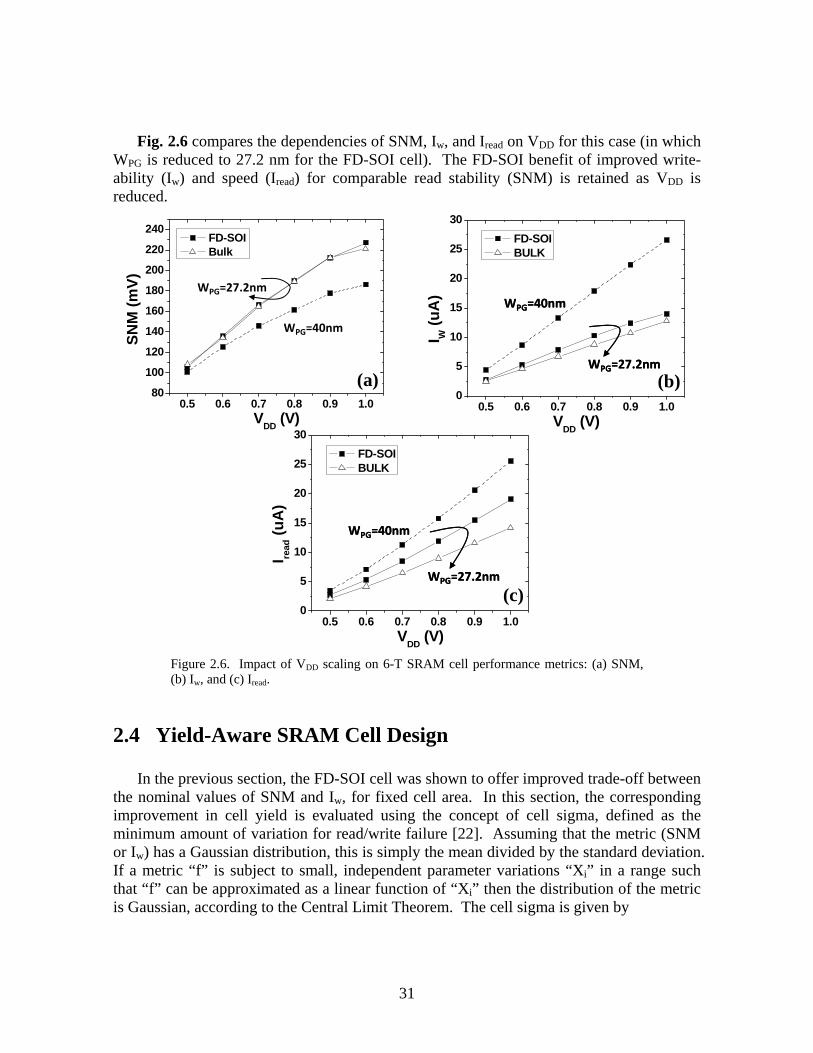
31
Fig. 2.6 compares the dependencies of SNM, Iw, and Iread on VDD for this case (in which WPG is reduced to 27.2 nm for the FD-SOI cell). The FD-SOI benefit of improved write-ability (Iw) and speed (Iread) for comparable read stability (SNM) is retained as VDD is reduced.
Figure 2.6. Impact of VDD scaling on 6-T SRAM cell performance metrics: (a) SNM, (b) Iw, and (c) Iread.
2.4 Yield-Aware SRAM Cell Design In the previous section, the FD-SOI cell was shown to offer improved trade-off between the nominal values of SNM and Iw, for fixed cell area. In this section, the corresponding improvement in cell yield is evaluated using the concept of cell sigma, defined as the minimum amount of variation for read/write failure [22]. Assuming that the metric (SNM or Iw) has a Gaussian distribution, this is simply the mean divided by the standard deviation. If a metric “f” is subject to small, independent parameter variations “Xi” in a range such that “f” can be approximated as a linear function of “Xi” then the distribution of the metric is Gaussian, according to the Central Limit Theorem. The cell sigma is given by
WPG=27.2nm
WPG=40nm
0.5 0.6 0.7 0.8 0.9 1.080
100
120
140
160
180
200
220
240
SNM
(mV)
VDD (V)
FD-SOI Bulk
0.5 0.6 0.7 0.8 0.9 1.00
5
10
15
20
25
30
I W (u
A)
VDD (V)
FD-SOI BULK
WPG=40nm
WPG=27.2nm
WPG=40nm
WPG=27.2nm
0.5 0.6 0.7 0.8 0.9 1.00
5
10
15
20
25
30
I read
(uA
)
VDD (V)
FD-SOI BULK
WPG=40nm
WPG=27.2nm
WPG=40nm
WPG=27.2nm
(a) (b)
(c)
32
2 2
(0)
( ) σ=
∂∂∑ ixi
i
fcell sigmafx
(2)
It should be noted that SNM and Iw each exhibit a linear response to small variations in Xi. Although their sensitivities can become non-linear for large variations (beyond several σXi), the most probable combination of variations in L, W, Tox and VTH does not exceed ~4σ variation in a single parameter. Thus, this method of estimating SRAM yield is reasonably accurate [22]. As explained above, random variations due to gate LER and RDF, as well as global (Gaussian) variations due to process-induced variations (±10%) in gate length, channel width, gate oxide thickness, and body thickness (Fig. 2.1(b)) are considered.
2.4.1 Iso-Area Comparison In the future, six-sigma (6σ) yield or larger will be required for large SRAM arrays to be functional. Fig. 2.7 shows the trade-off between Iw yield and SNM yield for FD-SOI and planar bulk cells, for VDD = 0.9V. (WPG is varied along the curves.) In order for a cell design to meet the 6σ yield requirement, both SNM and Iw must be able to tolerate at least 6 sigma variation. The FD-SOI cell can satisfy the 6σ yield requirement, and achieves maximum cell sigma with WPG = 40 nm. Approximately 10 nm variation in WPG can be tolerated, at this design point. In contrast, the planar bulk cell cannot satisfy the 6σ yield requirement. The optimal planar bulk cell design corresponds to WPG = 35 nm, and has ~1.2σ worse SNM yield and ~2.2σ worse Iw yield than the FD-SOI cell.
Figure 2.7. Yield of Iw vs. Yield of SNM. The optimal design points for planar bulk and FD-SOI cells are indicated (corresponding to WPG = 35 nm for the optimal planar bulk cell, and WPG = 40 nm for the optimal FD-SOI cell).
0 1 2 3 4 5 6 7 8 9 10 110123456789
1011
Yiel
d I w
(sig
ma)
Yield SNM (sigma)
FD-SOI BULK
VDD=0.9V
WPG=35nm + 1.20
+ 2.15
WPG=40nm
0 1 2 3 4 5 6 7 8 9 10 110123456789
1011
Yiel
d I w
(sig
ma)
Yield SNM (sigma)
FD-SOI BULK
VDD=0.9V
WPG=35nm + 1.20
+ 2.15
WPG=40nm

33
2.4.2 Iso-yield Comparison In order for the planar bulk cell to achieve >6σ yield, comparable to that of the optimized FD-SOI cell (with WPG = 40 nm), the pull-down and pull-up transistor widths must be increased to WPD = 95 nm and WPU = 50 nm, respectively, so that the cell area is increased by ~ 30% (from ~0.075 μm2 to ~0.1 μm2). In other words, the area savings offered by the FD-SOI cell is ~ 25%. The resultant Iw yield vs. SNM yield curve is plotted in Fig. 2.8, along with the curves from Fig. 2.7. The spot-lighted design point corresponds to WPG = 65 nm.
Figure 2.8. By up-sizing the planar bulk cell, yield that is comparable to that of the FD-SOI cell can be achieved. However, the trade-off between Yield of Iw and Yield of SNM is more severe for the planar bulk cell due to lower drive current and larger random VTH variation.
2.4.3 Minimum Operating Voltage (Vmin) for read and write operation By plotting Iw yield vs. SNM yield for various values of VDD, Vmin can be estimated. Figs. 2.9a and 2.9b show the impact of VDD reduction on yield, for the planar bulk and FD-SOI cells, respectively. At VDD ~ 0.6V the FD-SOI cell can no longer meet the 6σ criterion, i.e., Vmin ~ 0.6V. At VDD ~ 0.8V the increased-area planar bulk cell can no longer meet the 6σ criterion, i.e., Vmin ~ 0.8V. The FD-SOI cell achieves lower Vmin because it provides for higher transistor drive current and reduced variability. Table 2.4 summarizes the performance metrics of the FD-SOI and enlarged planar bulk SRAM cells at Vmin and nominal VDD.
0 1 2 3 4 5 6 7 8 9 10 110123456789
1011
Yiel
d I w
(sig
ma)
Yield SNM (sigma)
iso-area BULK iso-yield BULK FD-SOI
VDD=0.9V
0 1 2 3 4 5 6 7 8 9 10 110123456789
1011
Yiel
d I w
(sig
ma)
Yield SNM (sigma)
iso-area BULK iso-yield BULK FD-SOI
VDD=0.9V

34
Figure 2.9. Dependence of yield on VDD: (a) up-sized planar bulk cell (b) FD-SOI cell. At VDD ~ 0.8V, the planar bulk cell cannot satisfy the 6σ requirement, in contrast to the FD-SOI cell. Vmin is significantly lower, ~ 0.6 V, for the FD-SOI cell.
Table 2.4. Summary of SRAM cell performance metrics, for FD-SOI and enlarged planar bulk SRAM cells.
2.5 Summary Thin-BOX FD-SOI and planar bulk CMOSFET designs were optimized via 3-D process and device simulations, for LOP CMOS technology at the 22 nm node. For the same IOFF, the FD-SOI device achieves higher drive current and reduced random VTH variation. Using an analytical model fit to the simulated I-V characteristics for the optimized device designs, 6-T SRAM cell performance metrics (SNM, Iw, and Iread) were
0 1 2 3 4 5 6 7 8 9 10 110123456789
1011
Yi
eld
I w (s
igm
a)
Yield SNM (sigma)
Enlarged BULK (VDD=0.9V)
Enlarged BULK (VDD=0.8V)
Enlarged BULK (VDD=0.7V)
0 1 2 3 4 5 6 7 8 9 10 110123456789
1011
Yiel
d I w
(sig
ma)
Yield SNM (sigma)
FD-SOI (VDD=0.9V)
FD-SOI (VDD=0.8V)
FD-SOI (VDD=0.7V)
FD-SOI (VDD=0.6V)
(a) (b)
65
16.3
17.6
182
0.097
Vmin (= 0.8V)
Enlarged Planar bulk SRAM cell
40
20.6
22.4
178
0.075
VDD (=0.9V)
FD‐SOI SRAM cell
65
20.9
21.8
200
0.097
38
7.0
8.2
123
0.075
VDD (=0.9V)Vmin (= 0.6V)Supply voltage
WPG [nm] for maximum yield
Iread [μA]
Iw [μA]
SNM [mV]
Cell area [μm2]
65
16.3
17.6
182
0.097
Vmin (= 0.8V)
Enlarged Planar bulk SRAM cell
40
20.6
22.4
178
0.075
VDD (=0.9V)
FD‐SOI SRAM cell
65
20.9
21.8
200
0.097
38
7.0
8.2
123
0.075
VDD (=0.9V)Vmin (= 0.6V)Supply voltage
WPG [nm] for maximum yield
Iread [μA]
Iw [μA]
SNM [mV]
Cell area [μm2]

35
estimated. For fixed cell area, FD-SOI technology was found to provide for improved SNM yield (by 1.2σ), and Iw yield (by 2.2σ). For fixed yield, the FD-SOI cell provides an area savings of ~ 25%. The minimum operating voltage for 6σ yield (Vmin) is ~ 0.6V for the FD-SOI cell whereas it is >0.8V for the planar bulk cell. Thus, thin-BOX FD-SOI technology can facilitate the scaling of 6-T SRAM cell area and operating voltage. However, one practical drawback of FD-SOI technology is the higher cost of silicon-on-insulator (SOI) substrates. Therefore, in the subsequent chapters, a more cost-effective alternative transistor architecture will be discussed in detail.
2.6 References [1] K. J. Kuhn, “Reducing variation in advanced logic technologies: Approaches to process
and design for manufacturability of nanoscale CMOS,” IEDM Tech. Dig., Dec. 2007, pp. 471–474.
[2] A. Asenov, “Simulation of statistical variability in nano MOSFETs,” VLSI Symp. Tech. Dig., Jun. 2007, pp. 86–87.
[3] T. Ohtou, N. Sugii, and T. Hiramoto, “Impact of parameter variations and random dopant fluctuations on short-channel fully depleted SOI MOSFETs with extremely thin BOX,” IEEE Electron Device Lett., vol. 28, no. 8, pp. 740–742, Aug. 2007.
[4] C. Fenouillet-Beranger, S. Denorme, P. Perreau, C. Buj, O. Faynot, F. Andrieu, L. Tosti, S. Barnola, T. Salvetat, X. Garros, M. Casse, F. Allain, N. Loubet, L. Pham-Nguyen, E. Deloffre, M. Gros-Jean, R. Beneyton, C. Laviron, M. Marin, C. Leyris, S. Haendler, F. Leverd, P. Gouraud, P. Scheiblin, L. Clement, R. Pantel, S. Deleonibus, and T. Skotnicki, “FDSOI devices with thin BOX and ground plane integration for 32 nm node and below,” Solid State Electron., vol. 53, no. 7, pp. 730–734, Jul. 2009.
[5] T.-J. K. Liu, C. Shin, M. H. Cho, X. Sun, B. Nikolić, and B.-Y. Nguyen, “SRAM cell design considerations for SOI technology,” Proc. IEEE Int. SOI Conf., Oct. 2009, pp. 1–4.
[6] C. Shin, M. H. Cho, Y. Tsukamoto, B.-Y. Nguyen, B. Nikolić, and T.-J. K. Liu, “SRAM yield enhancement with thin-BOX FD-SOI,” Proc. IEEE Int. SOI Conf., Oct. 2009, pp. 1–2.
[7] Sentaurus User’s Manual, Synopsys, Inc., Mountain View, CA, 2009.06, Jun. 2009. [8] International Technology Roadmap for Semiconductors. [Online]. Available:
http://www.itrs.net [9] A. K. Rashimi and G. A. Armstrong, “Insights into gate-underlap design in double gate
based 6-T SRAM cell for low voltage applications,” Proc. IEEE Int. SOI Conf., Oct. 2008, pp. 61–62.
[10] K. Cheng, A. Khakifirooz, P. Kulkarni, S. Kanakasabapathy, S. Schmitz, A. Reznicek, T. Adam, Y. Zhu, J. Li, J. Faltermeier, T. Furukawa, L. F. Edge, B. Haran, S.-C. Seo, P. Jamison, J. Holt, X. Li, R. Loesing, Z. Zhu, R. Johnson, A. Upham, T. Levin, M. Smalley, J. Herman, M. Di, J.Wang, D. Sadana, P. Kozlowski, H. Bu, B.

36
Doris, and J. O’Neill, “Fully depleted extremely thin SOI technology fabricated by a novel integration scheme featuring implant-free, zero-silicon-loss, and faceted raised source/drain,” VLSI Symp. Tech. Dig., Jun. 2009, pp. 212–213.
[11] Y. Taur and T. H. Ning, Fundamentals of Modern VLSI Devices. Cambridge, U.K.: Cambridge Univ. Press, 2006.
[12] E. Seevinck, F. J. List, and J. Lohstroh, “Static-noise margin analysis of MOS SRAM cells,” IEEE J. Solid-State Circuits, vol. SSC-22, no. 5, pp. 748–754, Oct. 1987.
[13] C. Wann, R. Wong, D. J. Frank, R. Mann, S.-B. Ko, P. Croce, D. Lea, D. Hoyniak, Y.-M. Lee, J. Toomey, M. Weybright, and J. Sudijono, “SRAM cell design for stability methodology,” Proc. IEEE VLSI-TSA, Apr. 2005, pp. 21–22.
[14] E. Grossar, M. Stucchi, K. Maex, and W. Dehaene, “Read stability and write-ability analysis of SRAM cells for nanometer technologies,” IEEE J. Solid-State Circuits, vol. 41, no. 11, pp. 2577–2588, Nov. 2006.
[15] H. Dadgour, K. Endo, V. De, and K. Banerjee, “Modeling and analysis of grain-orientation effects in emerging metal-gate devices and implications for SRAM reliability,” IEDM Tech. Dig., Dec. 2008, pp. 705–708.
[16] A. Cathignol, B. Cheng, D. Chanemougame, A. R. Brown, K. Rochereau, G. Ghibaudo, and A. Asenov, “Quantitative evaluation of statistical variability sources in a 45-nm technological node LP N-MOSFET,” IEEE Electron Device Lett., vol. 29, no. 6, pp. 609–611, Jun. 2008.
[17] H. S. Yang, R. Wong, R. Hasumi, Y. Gao, N. S. Kim, D. H. Lee, S. Badrudduza, D. Nair, M. Ostermayr, H. Kang, H. Zhuang, J. Li, L. Kang, X. Chen, A. Thean, F. Arnaud, L. Zhuang, C. Schiller, D. P. Sun, Y. W. Teh, J. Wallner, Y. Takasu, K. Stein, S. Samavedam, D. Jaeger, C. V. Baiocco, M. Sherony, M. Khare, C. Lage, J. Pape, J. Sudijono, A. L. Steegen, and S. Stiffler, “Scaling of 32 nm low power SRAM with high-K metal gate,” IEDM Tech. Dig., 2008, pp. 233–236.
[18] H. Kawasaki, M. Khater, M. Guillorn, N. Fuller, J. Chang, S. Kanakasabapathy, L. Chang, R. Muralidhar, K. Babich, Q. Yang, J. Ott, D. Klaus, E. Kratschmer, E. Sikorski, R. Miller, R. Viswanathan, Y. Zhang, J. Silverman, Q. Ouyang, A. Yagishita, M. Takayanagi, W. Haensch, and K. Ishimaru, “Demonstration of highly scaled FinFET SRAM cells with high-K/metal gate and investigation of characteristic variability for the 32 nm node and beyond,” IEDM Tech. Dig., 2008, pp. 237–240.
[19] B. S. Haran, A. Kumar, L. Adam, J. Chang, V. Basker, S. Kanakasabapathy, D. Horak, S. Fan, J. Chen, J. Faltermeier, S. Seo, M. Burkhardt, S. Burns, S. Halle, S. Holmes, R. Johnson, E. McLellan, T. M. Levin, Y. Zhu, J. Kuss, A. Ebert, J. Cummings, D. Canaperi, S. Paparao, J. Arnold, T. Sparks, C. S. Koay, T. Kanarsky, S. Schmitz, K. Petrillo, R. H. Kim, J. Demarest, L. F. Edge, H. Jagannathan, M. Smalley, N. Berliner, K. Cheng, D. LaTulipe, C. Koburger, S. Mehta, M. Raymond, M. Colburn, T. Spooner, V. Paruchuri, W. Haensch, D. McHerron, and B. Doris, “22 nm technology compatible fully functional 0.1 μm2 6T-SRAM cell,” IEDM Tech. Dig., 2008, pp. 625–628.
[20] C. H. Diaz, K. Goto, H. T. Huang, Y. Yasuda, C. P. Tsao, T. T. Chu, W. T. Lu, V. Chang, Y. T. Hou, Y. S. Chao, P. F. Hsu, C. L. Chen, K. C. Lin, J. A. Ng, W. C. Yang, C. H. Chen, Y. H. Peng, C. J. Chen, C. C. Chen, M. H. Yu, L. Y. Yeh, K. S. You, K. S.

37
Chen, K. B. Thei, C. H. Lee, S. H. Yang, J. Y. Cheng, K. Y. Huang, J. J. Liaw, Y. Ku, S. M. Jang, H. Chuang, and M. S. Liang, “32 nm gate-first high-k/metal gate technology for high performance low power applications,” IEDM Tech. Dig., 2008, pp. 629–632.
[21] F. Arnaud, J. Liu, Y. M. Lee, K. Y. Lim, S. Kohler, J. Chen, B. K. Moon, C. W. Lai, M. Lipinski, L. Sang, F. Guarin, C. Hobbs, P. Ferreira, K. Ohuchi, J. Li, H. Zhuang, P. Mora, Q. Zhang, D. R. Nair, D. H. Lee, K. K. Chan, S. Satadru, S. Yang, J. Koshy, W. Hayter, M. Zaleski, D. V. Coolbaugh, H.W. Kim, Y. C. Ee, J. Sudijono, A. Thean,M. Sherony, S. Samavedam, M. Khare, C. Goldberg, and A. Steegen, “32 nm general purpose bulk CMOS technology for high performance applications at low voltage,” IEDM Tech. Dig., 2008, pp. 633–636.
[22] A. E. Carlson, “Device and circuit techniques for reducing variation in nanoscale SRAM,” Ph.D. dissertation, Univ. California Berkeley, Berkeley, CA, May 2008.
2.A Appendix
The analytical MOSFET I-V model used to estimate SRAM performance metrics in this work is:
2
0
( ) (1 ) (1 ) &2 1
( )(1 ) (1 ) & .... .(1)
1
(1 )
μ λ
μ λ
− −= + + − > ≥
−+
− −−
= + + − > <−
+
= −
DS
TH
DS
TH
DS GSTH
VVGS TH GS TH
DS s ox DS sub GS TH DSGS TH
sat
DSVDS GS THV GS TH
l ox DS sub GS TH DSGS TH
satV VV
sub
V V V VWI C V I e if V V VV VmL mE L
mVV V VV V VWC V I e if V V V EqV VL m
E L
I e e−
≤THV
SGS THif V V
where Cox is the gate oxide capacitance per area, L is the gate length, W is the device width, Isub is the current level corresponding to VTH, S is the sub-threshold swing, and VTH is the threshold voltage which is dependent on drain bias (VTH=VT0 – DIBL×VDS). μl and μs are the carrier mobility values in the linear and saturation regimes of operation, respectively. V0 is defined as 1/(1- μs/2μl). Esat is the saturation electric field, which determines the amount of velocity saturation. m is a fitting parameter. As experimentally verified in [22], this model accurately captures planar bulk MOSFET short-channel effects and operation in the sub-threshold, linear, and saturation regimes. So long as the analytical I-V model can be well fit to the simulated (or measured) I-V data for FD-SOI devices, it can accurately represent their behavior as well.

38
Chapter 3
Study of Random Dopant Fluctuation (RDF) Effects for the Quasi-Planar Bulk MOSFET
3.1 Introduction Threshold voltage (VTH) variation due to random dopant fluctuations (RDF) is already an issue for modern CMOS technologies [1], and will increase dramatically as MOSFET gate lengths are scaled below 30 nm [2]. To suppress VTH variation due to RDF, light channel surface doping achieved via a retrograde or delta-shaped body doping profile [3] or a thin-body (fully depleted) transistor structure [4, 5] should be used. Improved electrostatic integrity, e.g.,, via a reduction in equivalent gate oxide thickness (EOT) [6] or the use of a multiple-gate structure [7, 8], is beneficial for reducing the sensitivity of VTH to channel length and hence for reducing RDF-induced VTH variation as well. In this chapter, a modified atomistic simulation methodology [9] is used together with a commercial device simulator [10] to investigate the effects of randomly placed dopants in planar vs. quasi-planar bulk MOSFETs with 20 nm gate length (LG) and 20 nm layout width (W). The effects of body RDF vs. source/drain RDF are elucidated. VTH-adjustment approaches for the quasi-planar bulk MOSFET structure are compared with regard to robustness to RDF.

39
Figure 3.1. (a) 3D bird-eye view of the quasi-planar bulk MOSFET structure. The gate stack is not shown, in order to allow the channel region to be seen. (b) Cross-sectional view along the A-A’ line.
3.2 Device Simulation Approach
3.2.1 Nominal Bulk MOSFET Designs Based on the International Technology Roadmap for Semiconductors (ITRS) specifications, the nominal planar bulk MOSFET design is optimized using three-dimensional (3D) device simulations with continuum doping profiles, by selecting the electrical channel length (Leff, defined as the distance between the points where the source/drain doping profiles fall to 2 x 1019 cm-3), retrograde body doping peak depth (Tsi), and source/drain-extension (SDE) junction depth (XJ) to achieve maximum drive current for an effective oxide thickness (EOT) of 9 Å, gate work function (ΦM) of 4.08 eV (n+ poly-Si), and an off-state leakage current specification of 5 nA/μm at 1 V supply voltage (VDD). The vertical retrograde body and lateral SDE doping gradients are 4 nm/dec and 2 nm/dec, respectively. The parameters for the optimized design are Leff = 20 nm, Tsi = 14 nm, and XJ = 14 nm. Fig. 3.1 illustrates the nominal quasi-planar bulk MOSFET design. The physical height (Hsi) of the gated channel above the isolation-oxide surface is equal to Tsi to achieve the best performance [11], so that the physical channel width is 48 nm (W + 2Hsi). Note that the electrical effective channel width (Weff) is actually smaller (by ~8 nm) than this, because the retrograde body doping profile is not perfectly abrupt. ΦM is set to 4.35 eV for the quasi-planar device design to achieve the same linear VTH (0.34 V at VDS = 0.1V).
3.2.2 Methodology for Atomistic Device Simulation The methodology described in [9] was used to generate atomistic body- and SDE-doping profiles for 3D device simulation as follows. First, a pseudo-lattice structure in
A’
HSi = TSi
Isolation oxide
Source
Drain
Substrate
Spacer
A
A’
HSi = TSi
Isolation oxide
Source
Drain
Substrate
Spacer
A
Retrograde body doping
Xj=14nm
LG=20nm
Z [μm]
0 0.02X [μm]
0
0.04- 0.02- 0.04
4nm/dec
TSi
Retrograde body doping
Xj=14nm
LG=20nm
Z [μm]
0 0.02X [μm]
0
0.04- 0.02- 0.04
4nm/dec
TSi
(a) (b)

40
which each grid point represents a silicon atom is generated to represent the body and SDE regions. In other words, regions to be atomistically simulated are converted to cubic grids with the silicon lattice spacing. Then, the nominal doping profile information is used to calculate the probability of finding a dopant atom at each lattice site (PRDF). For each atomistic doping profile, a random probability following a uniform distribution (Prand) is generated for each lattice site, and a dopant atom is placed at every lattice site for which PRDF > Prand. The effective dopant concentration at each simulation mesh point is then calculated as follows. Rather than using a point charge definition of an ionized dopant atom, which would result in unrealistic singularities in potential and charge density, we followed the methodology of Sano et al. [12, 13] to model the “influence” of an ionized dopant atom, which decays as 1/r, where r is the radial distance from the center of the atom. Also, we used the long-range potential of a conduction electron in the silicon lattice to derive a corresponding charge density:
3
2 3
{sin( ) ( )cos( )}( )2 ( )
c c c c
c
qk k r k r k rrk r
ρπ−
= (1)
where kc is the inverse screen length or the inverse of the Debye length. For each randomly placed dopant atom, the distances to its eight nearest simulation mesh points are computed and the effective doping density contributed by the ionized dopant atom at these points is calculated using the long-range potential charge density [13]. This appropriately weights the influence of each ionized dopant atom at each simulation mesh point. Finally, an ASCII file containing the total doping density at each simulation mesh point is generated and exported to a commercial device simulator [10] for I-V simulation. An example of a quasi-planar bulk MOSFET structure with atomistic doping profiles is shown in Fig. 3.2. The sequence of random dopant placement and I-V simulation with advanced physical models including the density gradient model and drift-diffusion transport model [10] was iterated 200 times for each device design, in order to obtain meaningful VTH statistics.
Figure 3.2. (a) Example of a quasi-planar bulk MOSFET with atomistic doping profiles. (b) Isometric view of the same quasi-planar bulk MOSFET, showing the randomly placed dopant atoms.
Source
Drain
Gate
Source
Drain
Gate
(a) (b)
N+ N+
P-sub
Red; Acceptor atoms Blue: Donor atoms
N+ N+
P-sub
Red; Acceptor atoms Blue: Donor atoms

41
Figure 3.3. Simulated ID-VGS curves for bulk MOSFETs with atomistic body and source/drain doping profiles (200 cases each): (a) planar device design, and (b) quasi-planar device design. The thick square-dotted solid curves show the simulated ID-VGS curves obtained for continuum doping profiles. Note that the ID values are for devices with 20nm layout width. It took approximately 30 minutes for each ID-VGS curve simulation on an AMD64 machine with 8Gbit memory.
IDlin = 7.7 μA/20nm
σ(VTH) = 50.5 mV
<VTH> - VTH0 = -94.2 mV
(a) Planar Bulk MOSFET VDS = 0.1V
IDsat = 17 μA/20nm
σ(VTH) = 54.9 mV
<VTH> - VTH0 = -125.4 mV
IDsat = 32 μA/20nm σ (VTH) = 42.1 mV <VTH> - VTH0 = -96.7 mV
IDlin = 13 μA/20nm σ (VTH) = 35.4 mV <VTH> - VTH0 = -75.8 mV
(b) Quasi-Planar Bulk MOSFET
VDS = 1V
VDS = 0.1V VDS = 1V

42
3.3. Results and Discussion
3.3.1 Planar vs. Quasi-Planar Bulk MOSFET Designs Simulated ID-VGS curves for planar and quasi-planar MOSFETs with atomistic doping profiles are shown in Fig. 3.3 [14]. For reference, the curves obtained for the same devices with continuum doping profiles are also plotted. It can be seen that the variation in off-state current is reduced by one order of magnitude for the quasi-planar device. The standard deviation of VTH variation (σ(VTH)) for the quasi-planar device is ~70% that for the planar device, because the quasi-planar device has ~1.6× larger Weff (based on the ratio of ID,lin values) and only slightly greater depletion charge due to its 3D channel geometry. This can be also explained by the following equation for σ(VTH) [15], which is derived below:
( )2 /
BTH
effox stripe eff B
stripe
QV WC W L Q q
W
σ = (2)
where Cox is the areal gate capacitance, Wstripe is the layout width of a stripe, and QB is the depletion charge per unit layout area.
VTH is given by the well-known equation ,
2 BTH FB B
ox total
QV VC
ϕ= + + , where VFB is the
flat-band voltage, 2φB is the surface potential at the threshold condition, QB is the total depletion charge, and Cox,total is the total gate capacitance. Noting that
/ /(2 )B a B aQ N Q Nδ δ = since B aQ N∝ , it is derived from the above equation that
, , ,2 2a aB
TH B Box total a ox total a ox total
N nQV Q QC N C n C
δ δδδ = = = , where Na is the nominal doping
concentration, and na is the number of dopant atoms, in the depletion region. It is assumed that the actual number of dopant atoms follows a normal distribution, so that ( )a an nσ = .
Considering that BQ is the depletion charge per unit layout area and Cox is the areal gate capacitance, σ(VTH) for the quasi-planar bulk MOSFET is derived as follows.
, , ,
( )( )2 2 2
2 / 2 /
aa BTH B B
a ox total a ox total ox total a
B stripe eff B
effox eff eff stripe eff B ox stripe eff B
stripe
nn QV Q Qn C n C C n
Q W L QWC W L W L Q q C W L Q q
W
σσ = = =
= =
Note that Weff ≅Wstripe for the planar bulk MOSFET.

43
Figure 3.4. Comparison of body RDF vs. source/drain RDF effects on linear VTH (VDS = 0.1 V): (a) VTH lowering, (b) VTH variation. Note that VTH variation is reduced by ~30%, and that VTH variation due to body RDF is relatively suppressed, for the quasi-planar FET.
3.3.2 Body RDF vs. Source/Drain RDF To elucidate the impacts of body-RDF vs. source/drain-RDF, additional device simulations were performed with only atomistic body doping or only atomistic SDE doping (200 iterations for each case). From Fig. 3.4, it can be seen that both VTH lowering and VTH variation are dominated by body-RDF, because the position and number of dopant atoms in the body region are more important for determining VTH. Therefore, precise control of the body doping profile is critical for reducing VTH variation in bulk MOSFETs.
3.3.3 Assessment of VTH Adjustment Approaches For the quasi-planar bulk MOSFET, VTH can be adjusted by changing the body doping profile in two ways: by tuning its integrated dose, i.e., its peak concentration (Npeak), or its peak depth (Tsi). In order to compare the impacts of RDF for each VTH-adjustment method, additional atomistic device simulations were performed for the quasi-planar bulk MOSFET structure with the body doping profile tuned to adjust VTH either down to 0.15V or up to 0.4V (500 iterations for each VTH, for each method). For the conventional method of dose adjustment, σ(VTH) increases with VTH (Fig. 3.5a). In stark contrast, for the alternative method of Tsi adjustment, σ(VTH) does not increase significantly with VTH (Fig. 3.5b). This is expected based on Eq. 2, since the amount of depletion charge in the channel is increased significantly when Npeak is increased in order to increase VTH. Note that Weff decreases slightly with increasing Npeak, while Leff increases. Calculated values of σ(VTH) using Eq. 2 (with values for QB obtained by integrating the continuum retrograde body doping profile,
0
-20
-40
-60
-80
-100
(a)
Source/Drain RDFonly
Both RDF
<VTH
> - V
TH0 [m
V]
Body RDFonly
Planar FET Quasi-Planar FET
0
10
20
30
40
50
60
(b)
Source/Drain RDFonly
Both RDF
sigm
a (V
TH)
[mV]
Body RDFonly
Planar FET Quasi-Planar FET

44
values for Weff estimated from ID,lin, and values for Leff taken as the distance between the points where the source/drain doping profiles fall to 2 x 1019 cm-3) were found to match the values of σ(VTH) obtained via atomistic simulation, to within 5%, for the range of Npeak values in Fig. 3.5a. σ(VTH) was found empirically (from the atomistic simulations) to be proportional to QB
0.4 (rather than QB0.5 as in Eq. 2), consistent with findings in a previous
study [3]. When instead Tsi is decreased in order to increase VTH, the increase in QB (and hence the increase in σ(VTH)) is reduced. For the conventional method, a tradeoff in short-channel control (increased drain-induced barrier lowering) is seen as Npeak is reduced to lower VTH (Fig. 3.5a). For the alternative method, this tradeoff is less severe as Tsi is increased to lower VTH (Fig. 3.5b). Thus, VTH adjustment via tuning of the retrograde body doping depth is advantageous for mitigating tradeoffs in VTH variation and short-channel effect control. It should be noted that, for ease of process integration, a single value of Hsi (achieved by uniform selective etching to recess the isolation oxide, or by uniform selective epitaxial growth to elevate the channel) can be used for both low-VTH and high-VTH quasi-planar bulk MOSFETs. That is, the physical height of the channel can be the same for all quasi-planar devices, while the depth of the retrograde body doping is tuned (e.g.,, by adjusting the ion implantation energy) to adjust VTH to minimize the trade-off in VTH variation. Since this would result in Hsi > Tsi for the high-VTH devices, they would have proportionately larger intrinsic delay (due to larger gate-to-body capacitance); this should not present a serious issue, however, since high-VTH devices are not utilized in critical paths.
Figure. 3.5. Impact of nominal VTH adjustment on VTH variation. (a) Conventional VTH-adjustment method, with Hsi and Tsi each fixed at 14 nm. (b) Alternative VTH-adjustment method, with Npeak fixed at 2 × 1019 cm-3. The average value of drain-induced barrier lower (<DIBL>) is indicated for each design point. <DIBL> is tightly controlled within 100mV/V if the Tsi adjustment method is used.
2.0x10¹⁹ 4.0x10¹⁹ 6.0x10190
10
20
30
40
50
60
sigm
a (V
TH)
[mV]
<DIBL>= 120 mV/V
Peak doping concentration, Npeak[cm-3]
VTH=0.15V
<DIBL>= 50.5 mV/VVTH=0.34V
<DIBL>= 23 mV/VVTH=0.4V
HSi=TSi=14nm
10 12 14 16 180
10
20
30
40
50
60
VTH=0.4V
sigm
a(V TH
) [m
V]
TSi [nm]
<DIBL>= 33 mV/V
VTH=0.34V<DIBL>= 50.5 mV/V
VTH=0.15V<DIBL>= 76 mV/V
Npeak = 2 x 1019 cm-3
(a) (b)

45
3.4 Summary A study of random dopant fluctuation (RDF) effects on the quasi-planar bulk MOSFET vs. the planar bulk MOSFET is performed via atomistic three-dimensional device simulation, for devices with 20 nm gate length. The quasi-planar bulk MOSFET structure is more robust to RDF than a planar bulk MOSFET structure with identical nominal body and source/drain doping profiles and layout width. The effects of body RDF (vs. source/drain RDF) are dominant; hence, precise control of the body doping profile is critical for minimizing VTH variation in a bulk MOSFET technology. The quasi-planar bulk MOSFET offers a new method of VTH adjustment, via tuning of the retrograde body doping depth, to mitigate tradeoffs in VTH variation and short-channel effect control.
3.5 References [1] K. Takeuchi, T. Fukai, T. Tsunomura, A. T. Putra, A. Nishida, S. Kamohara, and T.
Hiramoto, “Understanding random threshold voltage fluctuation by comparing multiple fabs and technologies,” IEDM Tech. Dig., Dec. 2007, pp. 467–470.
[2] A. Asenov, “Simulation of statistical variability in nano MOSFETs,” IEEE Symp. VLSI Technol., Dig. Tech. Papers, Jun. 2007, pp. 86–87.
[3] A. Asenov and S. Saini, “Suppression of random dopant-induced threshold voltage fluctuations in sub-0.1-μm MOSFETs with epitaxial and δ-doped channels,” IEEE Trans. Electron Devices, vol. 46, no. 8, pp. 1718–1724, Aug. 1999.
[4] T. Ohtou, N. Sugii, and T. Hiramoto, “Impact of parameter variations and random dopant fluctuations on short-channel fully depleted SOI MOSFETs with extremely thin BOX,” IEEE Electron Device Lett., vol. 28, no. 8, pp. 740–742, Aug. 2007.
[5] K. Takeuchi, R. Koh, and T. Mogami, “A study of the threshold voltage variation for ultra-small bulk and SOI CMOS,” IEEE Trans. Electron Devices, vol. 48, no. 9, pp. 1995–2001, Sep. 2001.
[6] K. J. Kuhn, “Reducing variation in advanced logic technologies: Approaches to process and design for manufacturability of nanoscale CMOS,” IEDM Tech. Dig., Dec. 2007, pp. 471–474.
[7] Y. Li and S.-M. Yu, “Comparison of random-dopant-induced threshold voltage fluctuation in nanoscale single-, double-, and surrounding gate field-effect transistors,” Jpn. J. Appl. Phys., vol. 45, no. 9A, pp. 6860–6865, Sep. 2006.
[8] A. R. Brown, A. Asenov, and J. R. Watling, “Intrinsic fluctuations in sub 10-nm double-gate MOSFETs introduced by discreteness of charge and matter,” IEEE Trans. Electron Devices, vol. 1, no. 4, pp. 195–200, Dec. 2002.
[9] V. Varadarajan, L. Smith, S. Balasubramanian, and T.-J. King Liu, “Multigate FET design for tolerance to statistical dopant fluctuations,” Proc. Silicon Nanoelectronics Workshop, Jun. 2006, pp. 137–138.
[10] Sentaurus User’s Manual, Synopsys, Inc., Mountain View, CA. v. 2006.12.

46
[11] X. Sun, Q. Liu, V. Moroz, H. Takeuchi, G. Gebara, J. Wetzel, S. Ikeda, C. Shin, and T.-J. King Liu, “Tri-gate bulk MOSFET design for CMOS scaling to the end of the roadmap,” IEEE Electron Device Lett., vol. 29, no. 5, pp. 491–493, May 2008.
[12] N. Sano, K. Matsuzawa, M. Mukai, and N. Nakayama, “Role of long range and short-range Coulomb potentials in threshold characteristics under discrete dopants in sub-0.1 μm Si-MOSFETs,” IEDM Tech. Dig., Dec. 2000, pp. 275–278.
[13] T. Ezaki, T. Ikezawa, A. Notsu, K. Tanaka, and M. Hane, “3D MOSFET simulation considering long-range Coulomb potential effects for analyzing statistical dopant-induced fluctuations associated with atomistic process simulator,” Proc. SISPAD, Sep. 2002, pp. 87–90.
[14] C. Shin, A. Carlson, X. Sun, K. Jeon, and T.-J. King Liu, “Tri-gate bulk MOSFET design for improved robustness to random dopant fluctuations,” IEEE Silicon Nanoelectronics Workshop, Jun. 2008, pp. S1150.
[15] T. Mizuno, J.-I. Okamura, and A. Toriumi, “Experimental study of threshold voltage fluctuation due to statistical variation of channel dopant number in MOSFETs,” IEEE Trans. Electron Devices, vol. 41, no. 11, pp. 2216–2221, Nov. 1994.

47
Chapter 4
Full three-dimensional Simulation of 6-T SRAM Cells for the 22nm node
4.1 Introduction A challenge for continued SRAM cell area scaling is threshold voltage (VTH) mismatch due to variability in transistor performance [1], which eventually degrades the minimum operating voltage of the SRAM array [2]. To suppress VTH variation due to random dopant fluctuations (RDF) and process-induced variations in device parameters, light channel surface doping via a retrograde or delta-shaped body doping profile [3] or a fully-depleted ultra-thin-body/multi-gate architecture [4, 5] should be used. To avoid the need for expensive SOI substrates or more complex fabrication processes [6, 7], the segmented bulk MOSFET (SegFET) design was proposed to reduce VTH variation [8, 9]. In this chapter, the benefits of SegFET technology for 6T-SRAM are assessed via full 3-dimensional (3D) cell simulation, in contrast to conventional mixed-mode (device-circuit) simulation, with regard to read stability, write-ability, cell yield, and susceptibility to single-event-upset (SEU).

48
Figure 4.1. (a) Cross-sectional views of a two-striped SegFET (used for the pull-down devices in the SegFET SRAM cell) along one stripe and across the channel, (b) Front-end-of-line fabrication process steps for a SegFET.
(a)
(b)
1. Start with corrugated substrate
2. Define active areas
3. Fill trenches to formSTI; Implant wells STI
5. Implant channels;Form gate stack
6. Form S/D extensions, then sidewall spacers
7. Grow epitaxial materialin S/D regions (optional)
8. Dope S/D regions;Form silicide
1. Start with corrugated substrate
2. Define active areas
3. Fill trenches to formSTI; Implant wells
4. Slightly recess back STIor elevate stripes (optional)
5. Implant channels;Form gate stack
6. Form S/D extensions, then sidewall spacers
7. Grow epitaxial materialin S/D regions (optional)
8. Dope S/D regions;Form silicide
1. Start with corrugated substrate
2. Define active areas
3. Fill trenches to formSTI; Implant wells STI
5. Implant channels;Form gate stack
6. Form S/D extensions, then sidewall spacers
7. Grow epitaxial materialin S/D regions (optional)
8. Dope S/D regions;Form silicide
1. Start with corrugated substrate
2. Define active areas
3. Fill trenches to formSTI; Implant wells
4. Slightly recess back STIor elevate stripes (optional)
5. Implant channels;Form gate stack
6. Form S/D extensions, then sidewall spacers
7. Grow epitaxial materialin S/D regions (optional)
8. Dope S/D regions;Form silicide

49
4.2 Segmented Bulk MOSFET Structure and Fabrication Process The SegFET structure and front-end-of-line fabrication process steps are illustrated in Fig. 4.1. The channel is divided into stripes of equal width (WSTRIPE), with very shallow trench isolation (VSTI) regions in-between the stripes. The VSTI depth should be deeper than the source/drain extension junction depth (XJ) in order to fully suppress source-to-drain leakage current underneath the VSTI, but can be much shallower than the STI used to isolate transistors so that the channel stripes do not have a large aspect ratio. Within each stripe, the doping profiles are identical to those in a conventional planar bulk MOSFET (Fig. 4.1a). A quasi-planar structure is formed by recessing the VSTI by a small amount (HSTRIPE) prior to gate stack formation; together with a retrograde channel doping profile (peaked at a depth Tsi), it provides for superior electrostatic integrity. The SegFET fabrication process (Fig. 4.1b) is identical to a conventional bulk MOSFET fabrication process, except that a corrugated substrate is used as the starting material. Since the features on the corrugated substrate are geometrically very regular, small-pitch and high-resolution patterning techniques such as multiple patterning or spacer lithography [11] can be readily used to achieve stripes of uniform width with very fine pitch. For improved layout area efficiency, the stripe spacing (WSPACING) can be less than WSTRIPE.
4.3 6-T SRAM Cell Designs Fig. 4.2 shows the scaling trend for 6T-SRAM cell area. Based on recent publications [12-16], the dimensions for 22nm-node cells (Table 4.1) were selected for this study.
Figure 4.2. 6T-SRAM cell area scaling trend. The area of the proposed 22 nm node cell designs studied in this work is indicated.

50
Table 4.1. SegFET 6T-SRAM cell dimensions for the 22nm node. The half-bit cell layout and 6T SRAM circuit schematic are shown to indicate the parameters designated in the table.
The pull-up (α) ratio and cell (β) ratio of the SegFET SRAM cell design, with 2×WSTRIPE = 40nm, HSTRIPE = 10nm, and WSPACING = 15nm for the pull-down devices, are comparable to those of the other SRAM cell designs. The gate-sidewall spacer width (~10nm), with an upper limit imposed by the gate-to-contact pitch, and the source/drain extension junction depth (~10nm) are each optimized to achieve good static noise margin (SNM) [17] and write-ability current (Iw) [18]. To achieve the same VTH,lin as for the planar devices, the gate work-function is set to 4.3eV for the SegFETs. The SNM and Iw values for each cell design were obtained from full 3D simulations (Fig. 4.3) using advanced physical models including the density-gradient model and drift-diffusion transport model.
Figure 4.3. 3D 6-T SRAM cells simulation results: (a) butterfly plots and (b) write-N-curves for Planar, Quasi-Planar, and SegFET technologies. Each butterfly curve took ~6 hrs to simulate using an AMD64 machine (8 cores).
0.0 0.2 0.4 0.6 0.8 1.00
20
40
60
80
100
120
I n1 [
uA]
Vn1 [V]
Seg Quasi-Planar Planar
Iw Seg= 14.8 μA
Iw QP= 12.7 μA
Iw PL= 10.2 μA
0.0 0.2 0.4 0.6 0.8 1.00
20
40
60
80
100
120
I n1 [
uA]
Vn1 [V]
Seg Quasi-Planar Planar
Iw Seg= 14.8 μA
Iw QP= 12.7 μA
Iw PL= 10.2 μA
0.0 0.2 0.4 0.6 0.8 1.00.0
0.2
0.4
0.6
0.8
1.0
V n2 [V
]
Vn1 [V]
Seg Quasi-Planar Planar
SNM|Seg= 241.2mV
SNM|QP= 226.4mV
SNM|PL= 221.2mV
X
YLd
La
BC
Wl
D/2Wd
A/2
Wa
PG
PU PU
PDPDPG
n1 n2BL BLB
WLVDD
PG
PU PU
PDPDPG
n1 n2BL BLB
WLVDD
(a) (b)

51
Fig. 4.4 shows the 3D 6T-SRAM cell structures used in this study. The STI oxide is not shown in (a)-(c) to allow the channel regions to be seen. The STI oxide and VSTI oxide in-between multiple stripes of the pull-down SegFETs are shown in (d).
Figure 4.4. 3D 6T-SRAM cell structures with fine meshing (<1nm) in the channel regions.
As shown in Fig. 4.5, the SegFET cell has the highest SNM across the entire range of VDD values, and it is sufficient (≥0.2×VDD). The SNM at VDD = 1.1V is smaller for the quasi-planar cell as compared to the planar cell due to a weaker body effect in the pass-gate devices [10].
(a) Planar SRAM (b) TG bulk SRAM
(c) SegFET SRAM without Oxide (d) SegFET SRAM with STI and VSTI Oxide
PGPG
PDPD
PUPU
VSTI
PGPG
PUPUPDPD
PGPG
PDPD
PUPUPGPG
PUPUPDPD
PGPG
PDPD
PUPUPGPG
PUPUPDPD
(a) Planar SRAM (b) TG bulk SRAM
(c) SegFET SRAM without Oxide (d) SegFET SRAM with STI and VSTI Oxide
PGPG
PDPD
PUPU
VSTI
PGPG
PUPUPDPD
PGPG
PDPD
PUPUPGPG
PUPUPDPD
PGPG
PDPD
PUPUPGPG
PUPUPDPD
(a) Planar bulk SRAM (b) Quasi-Planar bulk SRAM
(c) SegFET SRAM without Oxide (d) SegFET SRAM with STI and VSTI Oxide
(a) Planar SRAM (b) TG bulk SRAM
(c) SegFET SRAM without Oxide (d) SegFET SRAM with STI and VSTI Oxide
PGPG
PDPD
PUPU
VSTI
PGPG
PUPUPDPD
PGPG
PDPD
PUPUPGPG
PUPUPDPD
PGPG
PDPD
PUPUPGPG
PUPUPDPD
(a) Planar SRAM (b) TG bulk SRAM
(c) SegFET SRAM without Oxide (d) SegFET SRAM with STI and VSTI Oxide
PGPG
PDPD
PUPU
VSTI
PGPG
PUPUPDPD
PGPG
PDPD
PUPUPGPG
PUPUPDPD
PGPG
PDPD
PUPUPGPG
PUPUPDPD
(a) Planar bulk SRAM (b) Quasi-Planar bulk SRAM
(c) SegFET SRAM without Oxide (d) SegFET SRAM with STI and VSTI Oxide

52
Figure 4.5. (a) SNM and (b) Iw vs. VDD. The SegFET cell has higher SNM across the range of VDD. The quasi-planar cell has better SNM at lower VDD (<0.9V), as compared to the planar cell.
4.4 Global and Local Variation Analysis Due to its superior electrostatic integrity, the SegFET is more robust to global and local variations. Figs. 4.6a and 4.6b compare short-channel effects and narrow-width effects, respectively, for the SegFET vs. planar MOSFET structures. Variation due to RDF was evaluated via atomistic simulations [9]: σ(VTH) ~ 25mV and 28mV for n-channel and p-channel SegFET/quasi-planar devices, respectively; σ(VTH) ~ 45mV and 49mV for the n-channel and p-channel planar devices, respectively. A sensitivity analysis was performed to assess the benefit of SegFET technology for improving SRAM cell yield using the concept of cell sigma, defined as the minimum amount of variation for read/write failure [10]. As shown in Fig. 4.6c, the SNM cell sigma for the SegFET cell is ~8, which is a 3-sigma improvement over the planar cell. The minimum VDD that meets the six-sigma yield requirement for both SNM and Iw is ~0.75V for the SegFET cell. In stark contrast, the six-sigma yield requirement cannot be met by the planar cell for any value of VDD; it achieves only 5.5 SNM cell sigma at VDD = 0.9V.
(a) (b)
0.4 0.6 0.8 1.0 1.2100
150
200
250
300
SN
M [m
V]
VDD [V]
Seg Quasi-Planar Planar
0.4 0.6 0.8 1.0 1.20
5
10
15
20
25
I W [u
A]
VDD [V]
Seg Quasi-Planar Planar

53
Figure 4.6. SegFET vs. planar MOSFET comparison: (a) VTH,lin vs. Lg (b) VTH,lin vs. W (c) SNM cell sigma (d) Iw cell sigma.
4.5 Simulation of Single-Event-Upset SRAM cell soft-error tolerance was evaluated using an inverter model in [19]. The high (“1”) storage node is the region of the cell that is most sensitive to a particle strike, because the drain junction of the corresponding pull-down device is reverse-biased so that the probability of collecting generated electron-hole-pairs (EHPs) in the drain depletion region is relatively high. In this work, soft-error tolerance is studied via transient simulation of complete 3D 6T-SRAM structures. First, the cell is written and then the data is held. Then, a heavy ion beam (Fig. 4.7) is made to vertically impinge on the high (“1”) storage node at time t = timpact, for each of the different SRAM cell designs. Due to the funneling effect [20], a parasitic thyristor turns on to short the drain node to the source node. This is evident in Figs. 4.8a and 4.8b, which show the high storage node (Vn1) voltage being pulled down as a result of the particle strike, so that the low storage node (Vn2)
20 40 60
0.2
0.4
0.6
0.8 single-striped SegFET planarFET
V TH,li
n [V]
LG [nm]
(a)
50 100 150 2000.2
0.3
0.4
0.5 single-striped SegFET planarFET
V TH,li
n [V]
W [nm]
(b)
0.4 0.6 0.8 1.0 1.20
1
2
3
4
5
6
7
8
9
10
SNM
Cel
l Sig
ma
[sig
ma]
VDD [V]
Seg Planar
0.4 0.6 0.8 1.0 1.20
1
2
3
4
5
6
7
8
9
10
SNM
Cel
l Sig
ma
[sig
ma]
VDD [V]
Seg Planar
(c)
0.4 0.6 0.8 1.0 1.20
1
2
3
4
5
6
7
8
9
10
I w C
ell S
igm
a [s
igm
a]
VDD [V]
Seg Planar
0.4 0.6 0.8 1.0 1.20
1
2
3
4
5
6
7
8
9
10
I w C
ell S
igm
a [s
igm
a]
VDD [V]
Seg Planar
(d)

54
voltage is increased due to the SRAM cell’s positive feedback. The simulation results indicate that the SegFET cell can withstand a particle strike with ~1.5× larger linear energy transfer (LET) value (~0.35pC/μm vs. ~0.24pC/μm for the planar cell) without data disturbance. This is because the SegFET cell has a stronger pull-up device (with ~40% higher on current), slightly higher (by <10%) source/drain junction capacitance, and smaller body effect [8]. Based on the “rule of thumb” that the maximum LET (in MeV-cm2/mg) of an ion beam is roughly equal to its atomic number Z, the SegFET cell is robust against much heavier particles (Zmax ~ 35). Note that if the beam incidence angle is decreased to 45o, the threshold LET value is reduced by 5-10%.
Figure 4.7. Heavy ion beam modeling. The Gaussian trace is characterized by the parameters lmax and w(t). It is assumed that the trace is symmetric with respect to the track axis.
Figure 4.8. Transient simulations of heavy-ion-beam strike on the high storage node in (a) SegFET 6T-SRAM cell, and (b) planar 6T-SRAM cell. lmax = 1um, w(t) = 5nm, incidence angle = 90o.
Heavy Ion Beam
Trace
lmax
W(t)
Heavy Ion Beam
Trace
lmax
W(t)W(t)
Voltage
[V]
0
0.9Vn1:Red dot‐line
Vn2:Blue solid‐line
Time [ns]timpact
1 3 75
Voltage
[V]
0
0.9Vn1:Red dot‐line
Vn2:Blue solid‐line
Time [ns]timpact
1 3 75
Time [ns]timpact
Voltage
[V]
0
0.9Vn1:Red dot‐line
Vn2:Blue solid‐line
1 3 75 Time [ns]timpact
Voltage
[V]
0
0.9Vn1:Red dot‐line
Vn2:Blue solid‐line
1 3 75
(a) (b)

55
4.6 Summary Full 3D 6T-SRAM cell simulations are used to assess the benefits of advanced MOSFET structures at the 22nm node. Segmented MOSFET (SegFET) technology is projected to achieve enhanced read stability and write-ability, improved SRAM cell yield, and improved immunity to soft errors.
4.7 References [1] E. Josse, S. Parihar, O. Callen, P. Ferreira, C. Monget, A. Farcy, M. Zaleski, D.
Villanueva, R. Ranica, M. Bidaud, D. Barge, C. Laviron, N. Auriac, C. Le Cam, S. Harrison, S. Warrick, F. Leverd, P. Gouraud, S. Zoll, F. Guyader, E. Perrin, E. Baylac, J. Belledent, B. Icard, B. Minghetti, S. Manakli, L. Pain, V. Huard, G. Ribes, K. Rochereau, S. Bordez, C. Blanc, A. Margain, D. Delille, R. Pantel, K. Barla, N. Cave, M. Haond, “A cost-effective low power platform for the 45-nm technology node,” IEDM Tech. Dig., Dec. 2006, pp. 1-4.
[2] K. Nii, M. Yabuuchi, Y. Tsukamoto, S. Ohbayashi, Y. Oda, K. Usui, T. Kawamura, N. Tsuboi, T. Iwasaki, K. Hashimoto, H. Makino, and H. Shinohara, “A 45-nm single-port and dual-port SRAM family with robust read/write stabilizing circuitry under DVFS environment,” VLSI Symp. Circuit Dig., Jun. 2008, pp. 212-213.
[3] A. Asenov, S. Saini, “Suppression of random dopant-induced threshold voltage fluctuations in sub-0.1-μm MOSFET’s with epitaxial and δ-doped channels,” IEEE Trans. Electron Devices, vol. 46, no. 8, pp. 1718-1724, Aug. 1999.
[4] K. Takeuchi, R. Koh, T. Mogami, “A study of the threshold voltage variation for ultra-small bulk and SOI CMOS,” IEEE Trans. Electron Devices, vol. 48, no. 9, pp. 1995-2001, Sep. 2001.
[5] K. J. Kuhn, “Reducing variation in advanced logic technologies: Approaches to process and design for manufacturability of nanoscale CMOS,” IEDM Tech. Dig., Dec. 2007, pp. 471–474.
[6] M. Jurczak, T. Skotnicki, M. Paoli, B. Tormen, J. Martin, J. L. Regolini, D. Dutartre, P. Ribot, D. Lenoble, R. Pantel, and S. Monfray, “Silicon-on-nothing (SON) – an innovative process for advacned CMOS,” IEEE Trans. Electron Devices, vol. 47, no. 11, pp. 2179-2187, Nov. 2000.
[7] T. Park, S. Choi, D. H. Lee, J. R. Yoo, B. C. Lee, J. Y. Kim, C. G. Lee, K. K. Chi, S. H. Hong, S. J. Hyun, Y. G. Shin, J. N. Han, I. S. Park, U. I. Chung, J. T. Moon, E. Yoon, and J. H. Lee, “Fabrication of body-tied FinFETs (Omega MOSFETs) using bulk Si wafers,” VLSI Symp. Tech. Dig., 2003, pp. 135-136.
[8] X. Sun, Q. Liu, V. Moroz, H. Takeuchi, G. Gebara, J. Wetzel, S. Ikeda, C. Shin, and T.-J. King Liu, “Tri-gate bulk MOSFET design for CMOS scaling to the end of the roadmap,” IEEE Electron Device Lett., vol. 29, no. 5, pp. 491–493, May 2008.

56
[9] C. Shin, A. Carlson, X. Sun, K. Jeon, and T.-J. King Liu, “Tri-gate bulk MOSFET design for improved robustness to random dopant fluctuations,” IEEE Silicon Nanoelectronics Workshop, Jun. 2008, pp. 1-2.
[10] A. Carlson, X. Sun, C. Shin, and T.-J. King Liu, “SRAM yield and performance enhancements with tri-gate bulk MOSFETs," IEEE Silicon Nanoelectronics Workshop, Jun. 2008, pp. 1-2.
[11] Y.-K. Choi, T.-J. King, and C. Hu, “A spacer patterning technology for nanoscale CMOS,” IEEE Trans. Electron Devices, vol. 49, no. 3, pp. 436-441, Mar. 2002.
[12] H. S. Yang, R. Wong, R. Hasumi, Y. Gao, N. S. Kim, D. H. Lee, S. Badrudduza, D. Nair, M. Ostermayr, H. Kang, H. Zhuang, J. Li, L. Kang, X. Chen, A. Thean, F. Arnaud, L. Zhuang, C. Schiller, D. P. Sun, Y. W. Teh, J. Wallner, Y. Takasu, K. Stein, S. Samavedam, D. Jaeger, C. V. Baiocco, M. Sherony, M. Khare, C. Lage, J. Pape, J. Sudijono, A. L. Steegen, and S. Stiffler, “Scaling of 32nm low Power SRAM with high-K metal gate,” IEDM Tech. Dig., 2008, pp. 233-236.
[13] H. Kawasaki, M. Khater, M. Guillorn, N. Fuller, J. Chang, S. Kanakasabapathy, L. Chang, R. Muralidhar, K. Babich, Q. Yang, J. Ott, D. Klaus, E. Kratschmer, E. Sikorski, R. Miller, R. Viswanathan, Y. Zhang, J. Silverman, Q. Ouyang, A. Yagishita, M. Takayanagi, W. Haensch, and K. Ishimaru, “Demonstration of highly scaled FinFET SRAM cells with high-K/metal gate and investigation of characteristic variability for the 32nm node and beyond,” IEDM Tech. Dig., 2008, pp. 237-240.
[14] B. S. Haran, A. Kumar, L. Adam, J. Chang, V. Basker, S. Kanakasabapathy, D. Horak, S. Fan, J. Chen, J. Faltermeier, S. Seo, M. Burkhardt, S. Burns, S. Halle, S. holmes, R. Johnson, E. McLellan, T. M. Levin, Y. Zhu, J. Kuss, A. Ebert, J. Cummings, D. Canaperi, S. Paparao, J. Arnold, T. Sparks, C. S. Koay, T. Kanarsky, S. Schmitz, K. Petrillo, R. H. Kim, J. Demarest, L. F. Edge, H. Jagannathan, M. Smalley, N. Berliner, K. Cheng, D. LaTulipe, C. Koburger, S. Mehta, M. Raymond, M. Colburn, T. Spooner, V. Paruchuri, W. Haensch, D. McHerron, and B. Doris, “22nm technology compatible fully functional 0.1μm2 6T-SRAM cell,” IEDM Tech. Dig., 2008, pp. 625-628.
[15] C. H. Diaz, K. Goto, H. T. Huang, Y. Yasuda, C. P. Tsao, T. T. Chu, W. T. Lu, V. Chang, Y. T. Hou, Y. S. Chao, P. F. Hsu, C. L. Chen, K. C. Lin, J. A. Ng, W. C. Yang, C. H. Chen, Y. H. Peng, C. J. Chen, C. C. Chen, M. H. Yu, L. Y. Yeh, K. S. You, K. S. Chen, K. B. Thei, C. H. Lee, S. H. Yang, J. Y. Cheng, K. Y. Huang, J. J. Liaw, Y. Ku, S. M. Jang, H. Chuang, and M. S. Liang, “32nm gate-first high-K/metal-gate technology for high performance low power applications,” IEDM Tech. Dig., 2008, pp. 629-632.
[16] F. Arnaud, J. Liu, Y. M. Lee, K. Y. Lim, S. Kohler, J. Chen, B. K. Moon, C. W. Lai, M. Lipinski, L. Sang, F. Guarin, C. Hobbs, P. Ferreira, K. Ohuchi, J. Li, H. Zhuang, P. Mora, Q. Zhang, D. R. Nair, D. H. Lee, K. K. Chan, S. Satadru, S. Yang, J. Koshy, W. Hayter, M. Zaleski, D. V. Coolbaugh, H. W. Kim, Y. C. Ee, J. Sudijono, A. Thean, M. Sherony, S. Samavedam, M. Khare, C. Goldberg, and A. Steegen, “32nm general purpose bulk CMOS technology for high performance applications at low voltage,” IEDM Tech. Dig., 2008, pp. 633-636.
[17] E. Seevinck, F. J. List, and J. Lohstroh, “Static-noise margin analysis of MOS SRAM cells,” Journal of Solid-State Circuits, vol. 22, no. 5, pp. 748-754, Oct. 1987.

57
[18] C. Wann, R. Wong, D. J. Frank, R. Mann, S.-B. Ko, P. Croce, D. Lea, D. Hoyniak, Y.-M. Lee, J. Toomey, M. Weybright, J. Sudijono, “SRAM cell design for stability methodology,” Proc. IEEE VLSI-TSA, Apr. 2005, pp. 21–22.
[19] K. Yamaguchi, Y. Takemura, K. Osada, K. Ishibashi, and Y. Saito, “3-D device modeling for SRAM soft-Error immunity and tolerance analysis,” IEEE Trans. Electron Devices, vol. 51, no. 3, pp. 378-388, Mar. 2004.
[20] K. Osada, K. Yamaguchi, Y. Saitoh, and T. Kawahara, “SRAM immunity to cosmic-ray-induced multierrors based on analysis of an induced parasitic bipolar effect,” Journal of Solid-State Circuits, vol. 39, no. 5, pp. 827-833, May 2004.

58
Chapter 5
Quasi-Planar Bulk CMOS Technology for Improved SRAM Scalability
5.1 Introduction Following Moore’s Law, transistor density has roughly doubled with each new CMOS technology generation largely due to the steady miniaturization of the transistor. Variation in transistor threshold voltage (VTH) due to random dopant fluctuations and line-edge-roughness [1] and gate work-function variation [2] become more significant as the transistor gate length (LG) is reduced below 30nm, so that continued transistor scaling poses a growing challenge, particularly for static random-access memory (SRAM) arrays which typically employ the smallest transistors and have the most stringent yield requirement [3]. VTH mismatch makes it difficult to lower the SRAM operating voltage [4], so that increasing power density has become a critical issue. Therefore, an improved transistor design that provides for reduced short-channel effects (i.e., improved gate control over the channel potential) and hence reduced VTH sensitivity to process-induced variations is needed to facilitate voltage scaling. Examples include the fully depleted silicon-on-insulator (FD-SOI) MOSFET with thin buried-oxide (thin-BOX) [5] and multiple-gate transistor structures (e.g.,, FinFET, MuGFET, Tri-Gate FET) [6]; but these require either expensive SOI substrates and/or more complex fabrication processes that pose significant barriers to their widespread adoption. Recently, a low-cost quasi-planar bulk CMOS technology was proposed and demonstrated to provide for improved performance and reduced variability [7, 8]. In contrast with FinFET/MuGFET/Tri-Gate FET structures which employ a narrow body region to suppress short-channel effects, the quasi-planar bulk MOSFET structure uses the conventional retrograde channel doping of the planar bulk

59
MOSFET structure to suppress leakage current, in addition to a quasi-planar gate electrode and gate fringing electric fields, to achieve improved gate control. This chapter presents more details of the study of quasi-planar bulk CMOS technology for improved SRAM scalability [8]. In Section 5.2, the device fabrication process is described. In Section 5.3, the benefits of the quasi-planar MOSFET design for improving transistor performance and reducing variability to improve SRAM yield are presented. Section 5.4 presents the conclusions from this study.
5.2 Device Fabrication (100) epi-Si wafers were used as the starting substrates for fabricating MOSFETs with <110> channel orientation in an early 28nm-generation bulk CMOS logic technology. The sequence of front-end-of-line fabrication process steps is outlined in Fig. 5.1. After conventional shallow-trench-isolation (STI) processing, N/P well and VTH-adjust ion implantation steps were performed, followed by high-temperature rapid thermal annealing (RTA). Subsequently, dilute hydrofluoric acid (DHF) was used to remove residual sacrificial oxide, as well as to recess the STI oxide by a small amount (15nm) prior to gate stack formation to achieve quasi-planar MOSFETs. A shorter DHF dip was used for the control (planar MOSFET) devices. The gate stack was formed by plasma nitridation of a thermal oxide layer of 1.45nm physical thickness followed by deposition of an undoped polycrystalline silicon layer of 70nm thickness. To define the gate electrodes with tight control of physical gate length (as small as 30nm) for logic transistors and 0.149μm2 6-T SRAM bit cells, a double-patterning/double-etch (2P2E) process employing 193nm immersion lithography and advanced hard-mask etching techniques was used. After gate stack patterning, pocket ion implantation was performed. An experimental split was included to explore lighter pocket doping, in which the implant dose was lowered by 1013cm-2. Gate-sidewall spacers were formed prior to source/drain ion implantation. To activate the implanted dopants, a rapid thermal process (RTP) followed by laser spike annealing (LSA) was used to enhance the electrical conductivity in the source/drain regions. Afterwards, a nickel silicidation (NiSi) process was applied. Subsequently, dual contact etch stop layers (CESL) of SiNx -- highly compressive stress liner for PMOS devices, and highly tensile stress liner for NMOS devices -- for performance enhancement were formed by plasma-enhanced chemical vapor deposition (PECVD). After interlayer dielectric (ILD) oxide deposition, contact hole definition, tungsten plug formation and chemical mechanical planarization (CMP), a standard copper metal interconnection process was followed. A standard test-chip mask set was used to fabricate individual logic transistors and 6T-SRAM arrays, ~2500 cells per device-under-test (DUT). Fig. 5.2 shows plan-view

60
scanning electron microscopy and cross-sectional transmission electron microscopy images of a fabricated SRAM cell.
Figure 5.1. Sequence of front-end-of-line CMOS fabrication process steps used to fabricate logic devices and SRAM arrays in this work. Figure 5.2. (a) 0.149μm2 SRAM cell plan-view CDSEM image after gate patterning. (b) XTEM taken along a poly-Si gate electrode in an SRAM array, for 15nm nominal STI-oxide recess depth.
STI Formation
Well & VTH Implantation
“STI Oxide Recess”
Gox/Poly-Si Deposition
Gate (2P2E) Patterning
LDD & Pocket Implantation
Spacer & S/D Formation
Activation Process
Salicidation
STI Formation
Well & VTH Implantation
“STI Oxide Recess”
Gox/Poly-Si Deposition
Gate (2P2E) Patterning
LDD & Pocket Implantation
Spacer & S/D Formation
Activation Process
Salicidation
570nm
263nm
570nm
263nmPG1
PD1 PU1
PU2 PD2
PG2(a)
570nm
263nm
570nm
263nmPG1
PD1 PU1
PU2 PD2
PG2
570nm
263nm
570nm
263nmPG1
PD1 PU1
PU2 PD2
PG2(a)

61
5.3 Results and Discussion
5.3.1 Quasi-Planar vs. Planar MOSFETs
5.3.1.1 Improved Performance Due to improved gate control and increased effective channel width, quasi-planar MOSFETs (in which the STI oxide is recessed by 15nm) have higher on-state drive current (ION) for comparable off-state leakage current (IOFF), as shown in Fig. 5.3. Lower pocket doping results in lower VTH as well as higher average effective mobility, and hence even higher ION. Because the benefit of sidewall gating increases as the layout width decreases, the pass-gate (PG) devices show greater improvement (2.4×) in ION than the pull-down (PD) devices (2.1× improvement). The performance enhancement (4.5×) is greatest for the PMOS devices not only because they have the narrowest layout width and but also because hole mobility is higher for the (110) sidewall channel surfaces, whereas electron mobility is lower [9].
Figure 5.3. Comparison of ON/OFF current statistics for planar (Control) vs. quasi-planar (RECESS=15nm) bulk MOSFETs in SRAM cells. (a) pass-gate NMOS ION, (b) pull-down NMOS ION, (c) pull-up PMOS ION.
0
5
10
15
20
25
30
35
40
Control RECESS=15nm RECESS=15nm(PKT Light)
Wafer
PG Id
sat (μA
)
0.149μm2 SRAM
σ = 3.43μA
σ = 6.64μA
σ = 4.64μA(Max, 0.75, Median,0.25, Min)
0
5
10
15
20
25
30
35
40
Control RECESS=15nm RECESS=15nm(PKT Light)
Wafer
PG Id
sat (μA
)
0.149μm2 SRAM
σ = 3.43μA
σ = 6.64μA
σ = 4.64μA(Max, 0.75, Median,0.25, Min)
0
5
10
15
20
25
30
35
40
Control RECESS=15nm RECESS=15nm(PKT Light)
Wafer
PD Id
sat (μA
)
0.149μm2 SRAM
σ = 3.68μA σ = 5.98μA σ = 4.26μA
(Max, 0.75, Median,0.25, Min)
0
5
10
15
20
25
30
35
40
Control RECESS=15nm RECESS=15nm(PKT Light)
Wafer
PD Id
sat (μA
)
0.149μm2 SRAM
σ = 3.68μA σ = 5.98μA σ = 4.26μA
(Max, 0.75, Median,0.25, Min)
-25
-20
-15
-10
-5
0
Control RECESS=15nm RECESS=15nm(PKT Light)
Wafer
PU Id
sat (μA
)
0.149μm2 SRAM
σ = 1.89μA
σ = 2.87μA σ = 2.74μA
(Max, 0.75, Median,0.25, Min)
-25
-20
-15
-10
-5
0
Control RECESS=15nm RECESS=15nm(PKT Light)
Wafer
PU Id
sat (μA
)
0.149μm2 SRAM
σ = 1.89μA
σ = 2.87μA σ = 2.74μA
(Max, 0.75, Median,0.25, Min)
(a)(b)
(c)

62
Figure 5.3. Comparison of ON/OFF current statistics for planar (Control) vs. quasi-planar (RECESS=15nm) bulk MOSFETs in SRAM cells. (d) pass-gate NMOS IOFF, (e) pull-down NMOS IOFF, (f) pull-up PMOS IOFF.
5.3.1.2 Suppressed VTH Variation VTH statistics are shown in Fig. 5.4 for the PG/PD/PU devices. Improved gate control results in steeper subthreshold swing and hence lower VTH for the quasi-planar MOSFETs. In this early 28nm CMOS process, the standard pocket implant dose is relatively high for the n-channel devices. As a result, variation in VTH is slightly larger for the quasi-planar PG and PD devices, due to more significant impact of random dopant fluctuations (RDF) for the gated sidewalls. This undesirable effect is eliminated by using a lighter pocket implant dose, as shown in Figs. 5.4a and 5.4b, which further lowers VTH without significantly increasing IOFF (ref. Figs. 5.3d and 5.3e). The standard pocket implant dose is lower for the p-channel devices, so that the impact of RDF for the gated sidewalls is not an issue. Thus, PMOS VTH variation is reduced when the STI oxide is recessed, due to the
0.01
0.1
1
10
100
Control RECESS=15nm RECESS=15nm(PKT Light)
Wafer
PG Io
ff (n
A)
0.149μm2 SRAM
σ = 1.22nA σ = 0.78nA σ = 0.52nA
(Max, 0.75, Median,0.25, Min)
0.01
0.1
1
10
100
Control RECESS=15nm RECESS=15nm(PKT Light)
Wafer
PG Io
ff (n
A)
0.149μm2 SRAM
σ = 1.22nA σ = 0.78nA σ = 0.52nA
(Max, 0.75, Median,0.25, Min)
0.01
0.1
1
10
100
Control RECESS=15nm RECESS=15nm(PKT Light)
Wafer
PD Io
ff (n
A)
0.149μm2 SRAM
σ = 5.84nA σ = 2.46nA σ = 2.46nA
(Max, 0.75, Median,0.25, Min)
0.01
0.1
1
10
100
Control RECESS=15nm RECESS=15nm(PKT Light)
Wafer
PD Io
ff (n
A)
0.149μm2 SRAM
σ = 5.84nA σ = 2.46nA σ = 2.46nA
(Max, 0.75, Median,0.25, Min)
0.001
0.01
0.1
1
10
Control RECESS=15nm RECESS=15nm(PKT Light)
Wafer
PU Io
ff (n
A)
0.149μm2 SRAM
σ = 38.0fA σ = 1.41nA σ = 1.08nA
(Max, 0.75, Median,0.25, Min)
0.001
0.01
0.1
1
10
Control RECESS=15nm RECESS=15nm(PKT Light)
Wafer
PU Io
ff (n
A)
0.149μm2 SRAM
σ = 38.0fA σ = 1.41nA σ = 1.08nA
(Max, 0.75, Median,0.25, Min)
(d) (e)
(f)

63
superior electrostatic integrity of the quasi-planar structure (Fig. 5.4c). If an even lighter pocket implant dose is used, then VTH variation is slightly larger due to degraded short-channel effect. In short, VTH variation in quasi-planar devices can be lower than in planar devices if the channel/pocket doping level is optimized.
Figure 5.4. Comparison of saturation VTH statistics for planar (Control) vs. quasi-planar (RECESS=15nm) bulk MOSFETs in SRAM cells: (a) pass-gate NMOS, (b) pull-down NMOS, (c) pull-up PMOS.
Pelgrom plots [10] showing how VTH variation increases with decreasing channel area, for logic devices, are shown in Fig. 5.5. Pelgrom’s coefficient (AVT) is reduced by 8% and 7% for the NMOS and PMOS quasi-planar devices with lower pocket doping, respectively. This improvement is consistent with the SRAM device results shown in Fig. 5.4.
0
0.1
0.2
0.3
0.4
0.5
0.6
0.7
0.8
0.9
Control RECESS=15nm RECESS=15nm(PKT Light)
Wafer
PG V
tsat
(V)
0.149μm2 SRAM
σ = 58.7mV σ = 67.2mV σ = 55.9mV
(Max, 0.75, Median,0.25, Min)
0
0.1
0.2
0.3
0.4
0.5
0.6
0.7
0.8
0.9
Control RECESS=15nm RECESS=15nm(PKT Light)
Wafer
PG V
tsat
(V)
0.149μm2 SRAM
σ = 58.7mV σ = 67.2mV σ = 55.9mV
(Max, 0.75, Median,0.25, Min)
0
0.1
0.2
0.3
0.4
0.5
0.6
0.7
0.8
0.9
Control RECESS=15nm RECESS=15nm(PKT Light)
Wafer PD
Vts
at (V
)
0.149μm2 SRAM
σ = 58.2mV σ = 61.1mV σ = 49.3mV
(Max, 0.75, Median,0.25, Min)
0
0.1
0.2
0.3
0.4
0.5
0.6
0.7
0.8
0.9
Control RECESS=15nm RECESS=15nm(PKT Light)
Wafer PD
Vts
at (V
)
0.149μm2 SRAM
σ = 58.2mV σ = 61.1mV σ = 49.3mV
(Max, 0.75, Median,0.25, Min)
0
0.1
0.2
0.3
0.4
0.5
0.6
0.7
0.8
0.9
Control RECESS=15nm RECESS=15nm (PKT Light)
Wafer
PU V
tsat
(V)
0.149μm2 SRAM
σ = 99.4mV σ = 60.4mV σ = 62.1mV
(Max, 0.75, Median,0.25, Min)
0
0.1
0.2
0.3
0.4
0.5
0.6
0.7
0.8
0.9
Control RECESS=15nm RECESS=15nm (PKT Light)
Wafer
PU V
tsat
(V)
0.149μm2 SRAM
σ = 99.4mV σ = 60.4mV σ = 62.1mV
(Max, 0.75, Median,0.25, Min)
(a) (b)
(c)

64
Figure 5.5. Pelgrom plots for (a) NMOS and (b) PMOS logic devices with drawn width ranging from 120nm to 1μm and drawn gate length ranging from 36nm to 0.2μm.
5.3.1.3 Improved Short-Channel Effect Fig. 5.6 shows the short-channel effect for logic devices with 250nm drawn width. It can be seen that VT roll-off is reduced for the quasi-planar structures, even though the channel is much wider (by >16×) than the STI oxide recess depth. Reasonable short-channel control is maintained by the quasi-planar structure even with lighter pocket doping.
Figure 5.6. Saturation threshold voltage with decreasing gate length, for logic devices with 0.25μm drawn width. (a) NMOS (b) PMOS.
y = 1.00x
y = 1.04x
y = 0.92x
0
2
4
6
8
10
12
14
16
18
0 5 10 15 20
1/sqrt(WL) [1/um]
Nor
mal
ized
σΔ
Vtlin
(A.U
.)
Control
RECESS=15nm
RECESS=15nm(PKT Light)
NMOS
y = 1.00 xy = 1.02x
y = 0.93x
02
468
101214
1618
0 5 10 15 20
1/sqrt(WL) [1/um]
Nor
mal
ized
σΔ
Vtlin
(A.U
.)
Control
RECESS=15nm
RECESS=15nm(PKT Light)
PMOS
NMOS
0.35
0.4
0.45
0.5
0.55
0.6
0.020 0.030 0.040 0.050 0.060
Lpoly (μm)
Vtsa
t (V)
Control
RECESS=15nm
RECESS=15nm(PKT Light)
NMOS
0.35
0.4
0.45
0.5
0.55
0.6
0.020 0.030 0.040 0.050 0.060
Lpoly (μm)
Vtsa
t (V)
Control
RECESS=15nm
RECESS=15nm(PKT Light)
PMOS
-0.5
-0.45
-0.4
-0.35
-0.3
-0.25
0.020 0.030 0.040 0.050 0.060
Lpoly (μm)
Vtsa
t (V)
Control
RECESS=15nm
RECESS=15nm(PKT Light)
PMOS
-0.5
-0.45
-0.4
-0.35
-0.3
-0.25
0.020 0.030 0.040 0.050 0.060
Lpoly (μm)
Vtsa
t (V)
Control
RECESS=15nm
RECESS=15nm(PKT Light)
(a) (b)
(a) (b)

65
5.3.1.4 Increased Narrow Width Effect The reverse narrow width effect, i.e., VTH reduction with decreasing channel width (W), stems from increased gate control for narrower channel width due to fringing electric fields between the gate electrode and channel sidewalls. This effect is intensified in quasi-planar devices, as shown in Fig. 5.7. It should be noted that, overall, VTH variation is lower for quasi-planar devices -- even with reduced pocket doping -- than for the planar devices, due to improved short channel control. To maximize the benefits of quasi-planar CMOS technology, wider transistors should be segmented into stripes of uniform width less than or equal to ~2LG [11]. A double-patterning approach [12] similar to that used for gate patterning in state-of-the-art CMOS processes can be used to form channel segments of highly uniform width without the need for forming high-aspect-ratio isolation trenches.
Figure 5.7. Measured reverse narrow width effect for devices with 36nm gate length: (a) NMOS (b) PMOS. Median VTH is lower when the STI oxide is recessed, due to improved gate control over the channel potential.
5.3.1.5 Compact Transistor Model One of the advantages of quasi-planar CMOS technology over FD-SOI and FinFET/MuGFET/Tri-Gate FET technologies is that it is compatible with standard bulk MOSFET compact models used for circuit design. In this work, the BSIM4.6 compact model was calibrated to the electrical characteristics of quasi-planar bulk MOSFETs, with fitting parameters including electrical and physical gate-oxide thickness, gate length offset,
NMOS Lg=0.036μm
0.2
0.25
0.3
0.35
0.4
0.45
0.5
0.55
0.6
0 0.2 0.4 0.6 0.8 1
Width (μm)
Vtsa
t (V)
CONTROL
RECESS=15nm
RECESS=15nm (PKT Light)
PMOS Lg=0.036μm
-0.5
-0.45
-0.4
-0.35
-0.3
-0.25
-0.2
-0.15
-0.1
0 0.2 0.4 0.6 0.8 1
Width (μm)
Vtsa
t (V)
CONTROL
RECESS=15nm
RECESS=15nm (PKT Light)
(b)(a)

66
and the number of fingers in the device. Fig. 5.8 shows that the compact model can be well-fitted to quasi-planar bulk MOSFET characteristics, including the body effect. This illustrates another advantage of quasi-planar CMOS technology, which is that it allows for adaptive body biasing, i.e., dynamic optimization of the trade-off between performance (delay) and power consumption (energy).
Figure 5.8. Comparison of measured output characteristics for planar (Control) vs. quasi-planar (RECESS=15nm) bulk MOSFETs in SRAM cells, for |VGS| = 1.0V. The effect of forward body biasing is also shown. (a) pass-gate NMOS, (b) pull-down NMOS, (c) pull-up PMOS. The symbols are measured data; the lines show the fitted compact model.
0
5
10
15
20
25
30
35
0 0.2 0.4 0.6 0.8 1Drain Voltage Vd (V)
PG D
rain
Cur
rent
Id (μ
A)
Control Vbs=0
Control Vbs=0.2
RECESS=15nm Vbs=0
RECESS=15nm Vbs=0.2
0
5
10
15
20
25
30
35
0 0.2 0.4 0.6 0.8 1
Drain Voltage Vd (V)
PD D
rain
Cur
rent
Id (μ
A) Control Vbs=0
Control Vbs=0.2
RECESS=15nm Vbs=0
RECESS=15nm Vbs=0.2
0
2
4
6
8
10
12
14
-1 -0.8 -0.6 -0.4 -0.2 0
Drain Voltage Vd (V)
PU D
rian
Cur
rent
Id (μ
A) Control Vbs=0
Control Vbs=-0.2
RECESS=15nm Vbs=0
RECESS=15nm Vbs=-0.2
(a) (b)
(c)

67
5.3.2 Benefits of Quasi-Planar Bulk CMOS Technology for 6T-SRAM
5.3.2.1 Cell Yield Enhancement In this early 28nm CMOS technology, SRAM yield (gauged by 3-sigma/mean values for DC read and write noise margins, SNM and WRM, respectively) was slightly diminished by recessing the STI oxide, because of the aforementioned increase in NMOS VTH variation (ref. Figs. 5.4a and 5.4b). If lighter pocket doping is used, however, variability is reduced so that yield is superior for the quasi-planar CMOS technology, as shown in Fig. 5.9. The nominal SNM is degraded by recessing the STI oxide because the cell beta ratio is degraded (even though the drive strength of the PU device is improved), which is why the increase in 3sigma/median is larger than for sigma (Fig. 5.9a). The fact that nominal WRM is improved by recessing the STI oxide accounts for the observation that 3sigma/median does not increase by very much, even though sigma increases significantly due to increased PG VTH variation (Fig. 5.9b).
Figure 5.9. Sigma and 3-sigma/median values for (a) read margin (SNM) and (b) write margin (WRM). Vdd = 1.0V.
5.3.2.2 Supply-Voltage Reduction Supply-voltage (Vdd) reduction is desirable to reduce power density and to facilitate increased transistor density. Generally, however, relative variability increases as the gate overdrive (Vdd-VTH) decreases, so that yield is degraded. Fig. 5.10 shows that the degradation in SNM yield with Vdd reduction (from 1.0V to 0.8V) is dramatically reduced for quasi-planar bulk CMOS technology with reduced pocket doping, while the degradation
40
45
50
55
60
65
Control RECESS=15nm RECESS=15nm(PKT Light)
Wafer
σ (m
V)
30%
35%
40%
45%
50%
3σ/
Med
ian
(%)
0.149μm2 SRAM WRM Vdd = 1.0V
40
45
50
55
60
65
Control RECESS=15nm RECESS=15nm(PKT Light)
Wafer
σ (m
V)
30%
35%
40%
45%
50%
3σ/
Med
ian
(%)
0.149μm2 SRAM WRM Vdd = 1.0V
10
15
20
25
30
35
40
Control RECESS=15nm RECESS=15nm(PKT Light)
Wafer
σ (m
V)
50%
55%
60%
65%
70%
75%
80%
3σ/
Med
ian
(%)
0.149μm2 SRAM SNM Vdd = 1.0V
10
15
20
25
30
35
40
Control RECESS=15nm RECESS=15nm(PKT Light)
Wafer
σ (m
V)
50%
55%
60%
65%
70%
75%
80%
3σ/
Med
ian
(%)
0.149μm2 SRAM SNM Vdd = 1.0V
(a) (b)
40 80%40 80%

68
in WRM yield with Vdd reduction is not significantly worse for quasi-planar bulk CMOS technology. With separately optimized pocket implant doses for the NMOS and PMOS devices, reduced degradation in both SNM yield and WRM yield with Vdd scaling can be achieved.
Figure 5.10. Degradation in 3-sigma/median for (a) SNM and (b) WRM as Vdd is reduced from 1.0V to 0.8V.
5.4 Summary With optimized pocket doping, quasi-planar MOSFETs achieved by slightly recessing the STI oxide prior to gate-stack formation in an otherwise conventional CMOS fabrication process can provide for improved performance and reduced variability, and hence can facilitate the scaling of SRAM operating voltage. The benefits of the quasi-planar bulk MOSFET design increase with decreasing channel width, so that quasi-planar CMOS technology is a compelling solution for future generations (22nm and beyond). As already discussed in the Chapter 2, fully-depleted silicon-on-insulator (FD-SOI) technology with thin buried-oxide (thin-BOX) provides for improved read-stability yield (by 1.2σ), and write-ability yield (by 2.2σ) for fixed SRAM cell area, as compared against planar bulk technology. For fixed yield, the FD-SOI SRAM cell provides a cell-area savings of ~ 25%. This benefit of area savings is offset by the incremental cost of an SOI substrate. In addition, established strain engineering techniques such as the use of embedded source/drain stressors cannot be used with FD-SOI technology, due to inherently ultra-shallow source/drain regions. In contrast, the quasi-planar bulk technology described herein offers a more cost-effective alternative, one that preserves the advantages of a conventional planar bulk technology (compatibility of strain engineering techniques to
0%
5%
10%
15%
20%
25%
30%
Control RECESS=15nm RECESS=15nm(PKT Light)
Wafer
3σ/M
edia
n D
egra
datio
n (%
) SNM 3σ/Median degradationfrom Vdd=1.0V to 0.8V
0%
5%
10%
15%
20%
25%
30%
Control RECESS=15nm RECESS=15nm(PKT Light)
Wafer
3σ/M
edia
n D
egra
datio
n (%
) SNM 3σ/Median degradationfrom Vdd=1.0V to 0.8V
0%
5%
10%
15%
20%
25%
30%
Control RECESS=15nm RECESS=15nm(PKT Light)
Wafer
3σ/M
edia
n D
egra
datio
n (%
) WRM 3σ/Median degradationfrom Vdd=1.0V to 0.8V
0%
5%
10%
15%
20%
25%
30%
Control RECESS=15nm RECESS=15nm(PKT Light)
Wafer
3σ/M
edia
n D
egra
datio
n (%
) WRM 3σ/Median degradationfrom Vdd=1.0V to 0.8V
(a) (b)

69
enhance mobility, dynamic threshold voltage control, an established compact device model, and low substrate cost) while offering the advantages of a multi-gate technology (improved performance and scalability). The benefits of quasi-planar bulk MOSFET technology will only increase with transistor scaling, since decreasing channel width results in improved electrostatic integrity, so that it is a compelling solution for CMOS scaling to the end of the technology roadmap (sub-10nm gate lengths).
5.5 References [1] A. Asenov, A. R. Brown, J. H. Davies, S. Kaya, and G. Slavcheva, “Simulation of
intrinsic parameter fluctuations in decananometer and nanometer-scale MOSFETs,” IEEE Trans. Electron Devices, vol. 50, no. 9, pp. 1837–1852, Sep. 2003.
[2] H. Dadgour, K. Endo, V. De, and K. Banerjee, “Modeling and analysis of grain-orientation effects in emerging metal-gate devices and implications for SRAM reliability,” IEDM Tech. Dig., 2008, pp. 705–708.
[3] K. A. Bowman, X. Tang, J. C. Eble, and J. D. Meindl, “Impact of extrinsic and intrinsic parameter fluctuations on CMOS circuit performance,” IEEE J. Solid-State Circuits, vol. 35, no. 8, pp. 1186–1193, Aug. 2000.
[4] K. Nii, M. Yabuuchi, Y. Tsukamoto, S. Ohbayashi, Y. Oda, K. Usui, T. Kawamura, N. Tsuboi, T. Iwasaki, K. Hashimoto, H. Makino, and H. Shinohara, “A 45-nm single-port and dual-port SRAM family with robust read/write stabilizing circuitry under DVFS environment,” VLSI Symp. Circuit Dig., 2008, pp. 212-213.
[5] C. Fenouillet-Beranger, S. Denorme, P. Perreau, C. Buj, O. Faynot, F. Andrieu, L. Tosti, S. Barnola, T. Salvetat, X. Garros, M. Casse, F. Allain, N. Loubet, L. Pham-Nguyen, E. Deloffre, M. Gros-Jean, R. Beneyton, C. Laviron, M. Marin, C. Leyris, S. Haendler, F. Leverd, P. Gouraud, P. Scheiblin, L. Clement, R. Pantel, S. Deleonibus, and T. Skotnicki, “FDSOI devices with thin BOX and ground plane integration for 32 nm node and below,” Solid State Electron., vol. 53, no. 7, pp. 730–734, Jul. 2009.
[6] H. Kawasaki, M. Khater, M. Guillorn, N. Fuller, J. Chang, S. Kanakasabapathy, L. Chang, R. Muralidhar, K. Babich, Q. Yang, J. Ott, D. Klaus, E. Kratschmer, E. Sikorski, R. Miller, R. Viswanathan, Y. Zhang, J. Silverman, Q. Ouyang, A. Yagishita, M. Takayanagi, W. Haensch, and K. Ishimaru, “Demonstration of highly scaled FinFET SRAM cells with high-K/metal gate and investigation of characteristic variability for the 32 nm node and beyond,” IEDM Tech. Dig., 2008, pp. 237–240.
[7] C. H. Tsai, T.-J. King Liu, S. H. Tsai, C. F. Chang, Y. M. Tseng, R. Liao, R. M. Huang, P. W. Liu, C. T. Tsai, C. Shin, B. Nikolić, C. W. Liang, “Segmented tri-gate CMOS technology for device variability improvement,” Proc. IEEE VLSI-TSA, Apr. 2010, pp. 114-115.
[8] C. Shin, C. H. Tsai, M. H. Wu, C. F. Chang, Y. R. Liu, C. Y. Kao, G. S. Lin, K. L. Chiu, C.-S. Fu, C.-T Tsai, C. W. Liang, B. Nikolić, T.-J. King, Liu, “Tri-gate bulk CMOS technology for improved SRAM scalability,” Proc. IEEE European Solid-State Device Research Conf. Sep. 2010, pp. 142–145.

70
[9] L. Chang, M. Ieong, and M. Yang, “CMOS circuit performance enhancement by surface orientation optimization,” IEEE Trans. Electron Devices, vol. 51, no. 10, pp. 1621–1627, Oct. 2004.
[10] M. J. M. Pelgrom, A. Duinmaijer, and A. Welbers, “Matching properties of MOS transistors,” IEEE J. Solid-State Circuits, vol. 24, no. 5, pp. 1433–1440, Oct. 1989.
[11] X. Sun, Q. Liu, V. Moroz, H. Takeuchi, G. Gebara, J. Wetzel, S. Ikeda, C. Shin, and T.-J. King Liu, “Tri-gate bulk MOSFET design for CMOS scaling to the end of the roadmap,” IEEE Electron Device Lett., vol. 29, no. 5, pp. 491–493, May 2008.
[12] U.S. patent 7,190,050.

71
Chapter 6
Performance and Yield Benefits of Quasi-Planar Bulk CMOS Technology for 6-T SRAM at the 22 nm Node
6.1 Introduction Efforts to reduce six-transistor (6-T) SRAM cell area [1-5] by a factor of two with each new technology generation are the de facto driving force for cutting-edge CMOS technology development. Continued SRAM cell area scaling is essential to sustaining Moore’s Law. However, it is challenged by both increased process-induced variability with transistor scaling and the need to integrate more cells on a die at each successive technology node. Specifically, a growing issue is transistor threshold voltage (VTH) mismatch due to systematic and random variations [6, 7], which sets a lower limit for the operating voltage of the SRAM array [8]. Variations in VTH caused by random dopant fluctuations (RDF) and gate line-edge-roughness (LER) will become dominant as the gate length (LG) is scaled down below 30 nm [9]. Various circuit- and transistor-design approaches have been proposed to address the issue of increasing VTH variation. These include the use of read-assist and write-assist techniques to enhance SRAM read and write margins, for example read/write-assist column circuitry, word-line bias, pulsed bit lines, and lower column supply voltages during write [10, 11] – which results in lower array efficiency (i.e., larger array layout area). Transistor-design approaches include the use of a super-steep retrograde or delta-shaped body doping profile [12], or the adoption of a transistor structure that provides for improved electrostatic integrity, such as fully depleted ultra-thin-body or multi-gate structures [13-15], to reduce

72
VTH sensitivity to variations. To avoid the need for costly silicon-on-insulator substrates or complex fabrication processes [16, 17], the quasi-planar bulk MOSFET design (Fig. 6.1) was recently proposed [18]. A simple approach for manufacturing this structure using a conventional CMOS process flow was recently demonstrated to provide for improved yield in an early 28 nm-generation SRAM technology [19, 20]: a timed dilute-HF etch is used to slightly recess the shallow trench isolation (STI) oxide just prior to gate-stack formation, resulting in gate electrodes that each wrap around the top portion of their respective MOSFET channel region. In this chapter, the potential benefits of quasi-planar bulk CMOS technology vs. planar bulk CMOS technology with regard to six-transistor (6-T) SRAM cell performance and yield are assessed, for the 22 nm technology node.
Figure 6.1. (a) Bird-eye view of a quasi-planar bulk MOSFET (gate electrode not shown to allow channel region to be seen), and its cross-sectional views (b) along and (c) across the channel.
STI
bSource
Drain
Substrate
Spacer
STI
bSource
Drain
Substrate
Spacer
STI
bSource
Drain
Substrate
Spacer
(a)
(b) (c)

73
6.2 Quasi-Planar Bulk Technology
6.2.1 Optimized MOSFET Performance Quasi-Planar bulk CMOSFET designs were optimized for gate length LG = 25 nm and transistor width WSTRIPE = 30 nm, using three-dimensional (3-D) device simulations, to achieve the highest on-state drive current (ION) for an off-state leakage current (IOFF) no greater than 3 nA/um, effective oxide thickness (EOT) Tox = 9 Å and VDD = 1V: electrical channel length (defined as the distance between the points where the source/drain extension (SDE) doping profiles fall to 2 x 1019 cm-3) Leff = 27 nm for NMOS, 28 nm for PMOS; source/drain extension (SDE) junction depth XJ,EXT = 10 nm; deep source/drain junction depth XJ,S/D = 28 nm; shallow-trench-isolation (STI) oxide recess depth (Hsi) = 10 nm; near-band-edge gate work functions ΦM = 4.2 eV for NMOS, 5.1 eV for PMOS. The retrograde channel doping profile is assumed to have a gradient of 4 nm/dec and peak doping concentration (Npeak) = 1019 cm-3 at a depth Tsi below the top channel surface; the SDE doping profile is assumed to have a steep lateral gradient of 2 nm/dec. Steep retrograde doping profiles have been achieved in practice via selective epitaxial growth of the lightly doped (or undoped) channel region [21-26] or by utilizing diffusion-barrier layers [27]. The same design parameter values are assumed for the planar bulk MOSFET design, except that ΦM = 4.08 eV for NMOS and 5.2 eV for PMOS to yield similar nominal values of saturation threshold voltage as their quasi-planar counterparts. Fig. 6.2 shows the transfer characteristics (IDS vs. VGS) for the optimized quasi-planar bulk and planar bulk MOSFET structures, with Tsi = 10 nm. The quasi-planar bulk devices exhibit steeper sub-threshold slopes due to better capacitive coupling between the gate and the channel region. A summary comparison of device performance parameters is given in Table 6.1. These simulation results are consistent with recently-reported experimental results [20] for devices which have worse electrostatic integrity (e.g.,, DIBL > 100 mV/dec), that have shown that quasi-planar bulk MOSFETs achieve higher ION at comparable IOFF -- and have lower VTH variation -- as compared to conventional planar bulk MOSFETs, so that they provide for improved SRAM yield. In this chapter, the planar bulk MOSFET design is optimized with very shallow SDE junction depths [28] to achieve very good electrostatic integrity – DIBL < 50 mV/V – to present the best-case scenario against which to compare the quasi-planar bulk MOSFET design. An analytical I-V model for the short-channel MOSFET [15] was fit to the simulated current-vs.-voltage characteristics. This model can be used to estimate SRAM performance metrics such as read static noise margin (SNM) [29, 31], static write margin expressed through the write-ability current (Iw) [30, 31], and read current. It is used in this work to estimate SRAM cell yield following the methodology described in [32].

74
Figure 6.2. Simulated transfer characteristics for (a) planar bulk and (b) quasi-planar bulk MOSFETs. To facilitate a direct comparison, the curves from (a) are overlaid in (b). The current is normalized to WSTRIPE + 2×Hsi.
Table 6.1. Summary of transistor performance parameters. The ON/OFF currents are normalized to WSTRIPE + 2×Hsi.
-1.0 -0.5 0.0 0.5 1.01E-10
1E-8
1E-6
1E-4
I D
S (A/u
m)
VGS (V)
Model I-V Simulated I-V (high VDS)
Simulated I-V (low VDS)
Planar Bulk
-1.0 -0.5 0.0 0.5 1.01E-10
1E-8
1E-6
1E-4
I D
S (A/u
m)
VGS (V)
Model I-V Simulated I-V (high VDS)
Simulated I-V (low VDS)
Planar Bulk
-1.0 -0.5 0.0 0.5 1.01E-10
1E-8
1E-6
1E-4
I DS (A
/um
)
VGS (V)
Model I-V Simulated I-V (high VDS)
Simulated I-V (low VDS)
Quasi‐planar Bulk
-1.0 -0.5 0.0 0.5 1.01E-10
1E-8
1E-6
1E-4
I DS (A
/um
)
VGS (V)
Model I-V Simulated I-V (high VDS)
Simulated I-V (low VDS)
Quasi‐planar Bulk
(a) (b)
46443733DIBL [mV/V]
27
0.13
0.17
85
2.2
786
N‐type
27
0.13
0.16
69
1.3
884
N‐type
Planar bulkQuasi‐planar bulkVDD= 1.0V
28
0.18
0.21
71
0.30
476
P‐type
28Leff [nm]
0.21|VTH,SAT| [V]
0.25|VTH,LIN| [V]
88SS [mV/dec]
0.44IOFF [nA/μm]
386ION [μA/μm]
P‐type
46443733DIBL [mV/V]
27
0.13
0.17
85
2.2
786
N‐type
27
0.13
0.16
69
1.3
884
N‐type
Planar bulkQuasi‐planar bulkVDD= 1.0V
28
0.18
0.21
71
0.30
476
P‐type
28Leff [nm]
0.21|VTH,SAT| [V]
0.25|VTH,LIN| [V]
88SS [mV/dec]
0.44IOFF [nA/μm]
386ION [μA/μm]
P‐type

75
6.2.2 Impact of Random and Systematic Variations The impact of random variations on transistor performance was studied via 3-D device simulations using realistic gate-electrode profiles and atomistic doping. Gate LER was simulated by sampling line-edge profiles from a scanning electron microscopy (SEM) image of photoresist lines printed for the 22 nm node. This represents the worst-case scenario, since the LER of a patterned gate electrode generally is less severe than that of the resist line used to define it. Also, the SDE junction lateral profiles are assumed to have the same LER as the gate electrode, so that Leff will have the same roughness profile as LG. In this manner, gate-LER-induced variations in VTH (i.e., σ(VTH)|gate-LER) were found to be = 31 mV for the planar bulk MOSFET and 16 mV for the quasi-planar bulk MOSFET with WSTRIPE/LG=30nm/25nm. Since the quasi-planar bulk MOSFET structure is an evolutionary form of the conventional planar bulk MOSFET structure [18] -- in contrast to the vertical FinFET/MuGFET structure -- it can be reasonably expected that gate-LER-induced variation for a quasi-planar bulk MOSFET would be very similar to that for a conventional planar bulk MOSFET. To verify this, LER-induced VTH variation for the various device architectures was compared: it was found that for the high-aspect-ratio FinFET/MuGFET, LER-induced VTH variation increases with decreasing correlation length due to increased misalignment between the front and back gates [33]; in contrast, for the low-aspect-ratio quasi-planar MOSFET and conventional planar MOSFET, LER-induced VTH variation decreases with decreasing correlation length due to an averaging effect. The methodology proposed by Sano [34], wherein only the long-range Coulomb potential for an ionized dopant atom is considered to avoid unrealistic singularities in potential profile, was used to simulate the effect of RDF for each of the gate-electrode profile cases. Details are described in [35], and only the results are summarized here: σ(VTH)|RDF = 54 mV for the planar bulk MOSFET and 30 mV for the quasi-planar bulk MOSFET with WSTRIPE/LG=30nm/25nm. Fig. 6.3a shows the distributions of saturation VTH (i.e., the value of VGS corresponding to 100 nA/um for VDS = 1 V) obtained from the simulated IDS-VGS curves (200 cases) for each device structure. The standard deviation of VTH variation (σ(VTH)) for the quasi-planar device is smaller than that for the planar device. This is due to improved suppression of short-channel effects (SCE) in the quasi-planar device, and the fact that it has ~1.6× larger effective channel width Weff (based on linear IDS values) but only slightly greater depletion charge [35]. Fig. 6.3b compares the VTH mismatch, gauged by the Pelgrom coefficient (AVT) [36], for the simulated devices in this work against that of experimental devices reported in the

76
literature. It can be seen that AVT for the planar bulk device design in this work follows the trend for planar bulk technologies. AVT of the quasi-planar bulk device design is improved, to be slightly worse than AVT for reported ultra-thin-body MOSFET technologies. The impacts of systematic variations (±10%) in LG, EOT, and WSTRIPE, are shown in Figs. 6.3c, 6.3d, and 6.3e, respectively. The short channel effect is better suppressed in the quasi-planar bulk MOSFET, due to improved gate control. This benefit is equivalent to >6 Å reduction in Tox. Also, variations in Tox have less impact for the quasi-planar bulk MOSFET. The quasi-planar bulk MOSFET shows a stronger reverse-narrow-width effect, but it is still less than 10 mV for 10% variation in WSTRIPE.
Figure 6.3. Simulated saturation threshold voltage (VTH,SAT) for planar bulk vs. quasi-planar bulk MOSFETs: (a) Distribution of VTH,SAT caused by gate-LER and RDF (for WSTRIPE/LG=30nm/25nm), from which σ(VTH,SAT|Planar Bulk) = 61.6 mV and σ(VTH,SAT|QP
Bulk) = 33.1 mV, (b) Comparison of Pelgrom coefficients for simulated vs. experimental reported devices. (c) VTH,SAT vs. LG, (d) VTH,SAT vs. Tox,
-0.1 0.0 0.1 0.2 0.30
50
100
150
200 QP Bulk Planar Bulk
Cou
nt (#
)
VTH,SAT (V)
22.5 25.0 27.50.00
0.05
0.10
0.15
0.20
V TH,S
AT (V
)
Gate Length (nm)
QP Bulk (Tsi= 6nm, Hsi=10nm)
QP Bulk (Tsi= Hsi=10nm)
Planar Bulk (Tsi= 10nm) QP Bulk (Tsi= 14nm, Hsi=10nm)
7 8 9 10 110.00
0.05
0.10
0.15
0.20
QP Bulk (Tsi= 6nm, Hsi=10nm)
QP Bulk (Tsi= Hsi=10nm)
Planar Bulk (Tsi= 10nm) QP Bulk (Tsi= 14nm, Hsi=10nm)
V TH,S
AT (V
)
Gate Oxide Thickness (A)
(a) (b)
(c) (d)
10 20 30 400.0
0.5
1.0
1.5
2.0
2.5
3.0
3.5
4.0
22nm Planar Bulk (this work)
22nm Quasi-Planar (this work)
IBM 22nmLETI 20nm
LETI 30nm
IBM 32nmIntel 45nm
Intel 65nm
Bulk Platform FD-SOI/ETSOI This work
AVT
= σ
(ΔV TH
) x
sqrt
(LW
) (m
V x
um)
Gate Length (nm)
ST 45nm

77
Figure 6.3. Simulated saturation threshold voltage (VTH,SAT) for planar bulk vs. quasi-planar bulk MOSFETs: (e) VTH,SAT vs. WSTRIPE. Note that the quasi-planar bulk MOSFET shows less sensitivity to variations in gate length (LG) and gate-oxide thickness (Tox), and that the depth of the retrograde channel doping profile (Tsi) can be used to tune the threshold voltage without impacting short-channel control. The quasi-planar bulk MOSFET shows more sensitivity to variations in transistor width, if WSTRIPE is small (30 nm).
6.3 Notchless 6-T SRAM Cell Designs Layout parameters for 22 nm 6-T SRAM cells (Fig. 6.4) were selected based on recent publications [1-5] and are summarized in Table 6.2. Nominal SNM and IW values were obtained via 3-D simulations of full cell structures using advanced physical models including the density-gradient/drift-diffusion transport model and the phenomenological van Dort quantum correction model to account for energy quantization in the channel regions. In a conventional SRAM cell layout (Fig. 6.4a), the width of the NMOS pull-down (PD) device is larger than the width of the NMOS pass-gate (PG) device, to achieve a cell beta ratio greater than 1 for sufficient nominal SNM. As a result, the NMOS active area pattern is notched. Due to limitations of optical lithography the corners of the active area will be rounded in practice, so that (vertical) misalignment between the gate layer and the active layer results in asymmetric variations in NMOS device width (i.e., mismatch) between the left and right sides of the cell, which can significantly degrade SNM [39]. An advantage of the quasi-planar bulk MOSFET design is that it allows for VTH to be adjusted by tuning the depth (Tsi) -- rather than the dose (Npeak) -- of the retrograde channel doping profile, without increasing either short-channel effects or VTH variation [35]. (Note that fringing electric fields through the isolation oxide allow good gate control to be
24 27 30 33 36 39 42 45 48 510.00
0.05
0.10
0.15
0.20
QP Bulk (Tsi= 6nm, Hsi=10nm)
QP Bulk (Tsi= Hsi=10nm)
Planar Bulk (Tsi= 10nm) QP Bulk (Tsi= 14nm, Hsi=10nm)
V TH,S
AT (V
)
WSTRIPE (nm)
(e)

78
maintained even if Tsi is slightly larger than Hsi.) This remarkable feature can be exploited to tune the SRAM cell beta ratio by adjusting transistor VTH values rather than transistor widths, so that a notchless active area pattern (Fig. 6.4b) can be used. A notchless cell design can provide for area savings as well as reduced variation in NMOS device width resulting from lithographic misalignment, due to improved printability of the active area pattern. To achieve sufficient SNM with a notchless quasi-planar SRAM cell design, the NMOS pull-down and PMOS pull-up (PU) devices should have lower VTH values than the NMOS pass-gate device. This is achieved with a deeper retrograde channel doping profile (ref. Figs. 6.3c-6.3e) which could be achieved in practice by using a higher ion-implantation energy. Note that Hsi is constrained to be the same for all of the devices in a quasi-planar SRAM cell for ease of manufacture, i.e., the isolation oxide is uniformly recessed (e.g.,, by using a timed etch in dilute hydrofluoric acid solution, or by elevating the channel with a selective epitaxial growth process) prior to gate-stack formation1. Further note that the transistor widths (WPU, WPD, and WPG) are constrained to be equal in a notchless cell design, so as to be compatible with a regularly corrugated starting substrate [40] for improved active-area width control.
Figure 6.4. Half-bit cell layouts for (a) notched and (b) notchless SRAM cell designs.
PD
PG
PUX
YLPD
LPG
BC
WPU
D/2WPD
A/2
WPG
PD
PG
PUX
YLPD
LPG
BC
WPU
D/2WPD
A/2
WPG
PD
PG
PUX
YLPD
LPG
BC
WPU
D/2WPD
A/2
WPG
PD
PG
PUX
YLPD
LPG
BC
WPU
D/2WPD
A/2
WPG
(a) (b)

79
Table 6.2. 22nm-node 6-T SRAM cell layout parameters for planar bulk and quasi-planar bulk CMOS technologies.
As can be seen from Fig. 6.5, the small notchless quasi-planar SRAM cell achieves comparable SNM and superior write-ability as compared against a conventional notched planar SRAM cell. Significantly larger read current is offered by the quasi-planar SRAM cell designs across a wide range of VDD (Fig. 6.6a). Although gate capacitance is also higher for the quasi-planar SRAM cell designs (Fig. 6.6b), simulations of the storage-node transient voltage during a write operation (Fig. 6.6c) show that the write time is still shorter for the quasi-planar SRAM cell designs.
Figure 6.5. 3-D 6-T SRAM cell simulation results for the planar bulk, quasi-planar bulk, and notchless quasi-planar bulk SRAM cells: (a) Butterfly curves, (b) write-N-curves.
50DDIF-DIF (min)
0.0741 / 0.0646 / 0.0745 μm2A SRAM cell area
390 / 340 / 392Total
10HsiHsi for quasi-planar
50CN/P isolation
30 / 30 / 43WPUPU width
30 / 30 / 43WPGPG width
55 / 30 / 43WPDPD Width
20BPOLY-to-DIF ext
30APOLY-to-POLY
Cell Width
190Total
20YGate-to-CONT
30XCONT size
25LPDPD CH length
25LPGPG CH length
Cell Height
Size [nm]SymbolDesign rules
0.0 0.2 0.4 0.6 0.8 1.00.0
0.2
0.4
0.6
0.8
1.0
V n2 (V
)
Vn1 (V)
QP Bulk Small Notchless QP Notchless QP Planar Bulk
0.0 0.2 0.4 0.6 0.8 1.00
20μ
40μ
60μ
80μ
100μ
I n1 (A
)
Vn1 (V)
QP Bulk Small Notchless QP Notchless QP Planar Bulk
(a) (b)

80
Figure 6.6. (a) SRAM cell read current, (b) PD device gate capacitance, (c) Pseudo-transient simulation of the storage-node voltage during a write operation.
Table 6.3 summarizes the projected cell performance metrics and cell area values for the planar and quasi-planar SRAM cells. Since VTH is lower for the PD and PU devices in the small notchless quasi-planar cell, it has higher standby power consumption (Pstandby) than the planar (notched) cell. Pstandby can be lowered by increasing VTH for all of the transistors in the notchless quasi-planar cell, but then the transistors must be widened to maintain a comparable level of performance and yield, i.e., there would be no area savings in comparison with the notched cell design. The devices in an optimized notchless quasi-planar cell design have shallower retrograde channel doping depths of 10/6/10 nm for PD/PG/PU and widths of 43 nm.
0.4 0.6 0.8 1.0 1.205
1015202530354045
I re
ad (u
A)
VDD (V)
QP Bulk Small Notchless QP Notchless QP Planar Bulk
-1.0 -0.5 0.0 0.5 1.00
20a
40a
60a
80a
100a
120a
0
20a
40a
60a
80a
100a
120a
Cgg
(F)
VGS (V)
QP Bulk (Tsi = Hsi = 10nm)
QP Bulk (Tsi = 14nm, Hsi = 10nm)
QP Bulk (Tsi = 6nm, Hsi = 10nm)
Planar Bulk(a) (b)
0 1 2 3 4 5 6 7 80.01
0.1
1
V stor
age_
node
(V)
Time (ps)
QP Bulk Small Notchless QP Notchless QP Planar Bulk
(c)

81
Table 6.3. Comparison of projected performance metrics and cell areas for planar bulk and quasi-planar bulk SRAM cells at VDD = 0.9V.
6.4 SRAM Yield Estimation In the previous section, the quasi-planar bulk SRAM cell designs were shown to have improved static performance (i.e., better read stability and write-ability current) and better transient performance (i.e., shorter write time). In this section, the corresponding improvement in cell yield is evaluated using the concept of cell sigma, defined as the minimum amount of variation for read/write failure [32]. If a SRAM cell read/write metric has a Gaussian distribution, its cell sigma is simply its mean value divided by its standard deviation. Random variations due to gate-LER, RDF, and WFV, as well as global variations due to process-induced variations (Gaussian with 3 sigma corresponding to ±10%) in gate length, stripe width, gate oxide thickness, and channel stripe height (Hsi) are considered together in estimating the cell sigma. Although σ(VTH,LIN) is generally smaller than σ(VTH,SAT), the worst-case scenario σ(VTH,LIN) = σ(VTH,SAT) is assumed herein. Six-sigma (6σ) yield is required for large SRAM arrays to be functional, i.e., no more than one bit cell can fail out of 505 million bit cells to achieve sufficiently high chip yields.
6.4.1 Iso-Area and Iso-Yield Comparisons between Planar and Quasi-Planar Bulk Cell Designs As shown in Fig. 6.7, the SNM cell sigma for the quasi-planar cell is ~6.3 at VDD = 0.9V, which is a 1.3-sigma improvement over the planar cell. This yield enhancement can be attributed primarily to lower VTH variation for the quasi-planar MOSFET structure. The minimum VDD that meets the six-sigma yield requirement for both SNM and IW is ~ 0.65V for the quasi-planar cell. In stark contrast, the six-sigma yield requirement cannot be met by the planar cell for any value of VDD; it achieves only ~5 SNM cell sigma at VDD = 0.9V. In order for the planar cell to have read and write yields comparable to those of the quasi-planar cell, the widths of the PD, PG and PU transistors must be increased to 110 nm,
0.1070.074522.3182.7Notchless Quasi‐planar Bulk(WSTRIPE = 43nm, Tsi for PD/PG/PU = 10/6/10nm, Hsi = 10nm)
0.2180.074116.4180.5Planar Bulk
0.3510.064620.5175.6Small Notchless Quasi‐planar Bulk(WSTRIPE = 30nm, Tsi for PD/PG/PU = 14/10/14nm, Hsi = 10nm)
0.0741
Cell area [μm2]
24.1
Iw [μA]
0.186
Pstandby per bit [nW]SNM [mV]Technology
183.5Quasi‐planar Bulk

82
65 nm and 65 nm, respectively. The planar cell area must therefore be enlarged to ~ 0.1 μm2 by ~ 46%. In other words, the area savings offered by the quasi-planar cell design is ~ 32%.
Figure 6.7. SRAM cell sigma comparisons for (a) SNM and (b) IW.
6.4.2 Notchless Quasi-Planar Bulk SRAM Cell Yield As can be seen from Fig. 6.8, the notchless quasi-planar cell can meet the 6-sigma yield requirements for VDD down to ~0.8V, with comparable cell area and faster write time as compared to the conventional planar cell (ref. Fig. 6.6c). The small notchless quasi-planar cell (with ~13% smaller area) is projected to meet the 6-sigma cell yield requirement for VDD down to ~0.9V.
Figure 6.8. SRAM cell sigma comparisons for (a) SNM and (b) IW.
0.4 0.6 0.8 1.0 1.20123456789
SNM
Cel
l Sig
ma
(sig
ma)
VDD (V)
QP Bulk Enlarged Planar Bulk Planar Bulk
~ 1.3σ
0.4 0.6 0.8 1.0 1.20123456789
SNM
Cel
l Sig
ma
(sig
ma)
VDD (V)
QP Bulk Enlarged Planar Bulk Planar Bulk
0.4 0.6 0.8 1.0 1.20123456789
SNM
Cel
l Sig
ma
(sig
ma)
VDD (V)
QP Bulk Enlarged Planar Bulk Planar Bulk
~ 1.3σ
0.4 0.6 0.8 1.0 1.20123456789
I w C
ell S
igm
a (s
igm
a)VDD (V)
QP Bulk Enlarged Planar Bulk Planar Bulk
0.4 0.6 0.8 1.0 1.20123456789
I w C
ell S
igm
a (s
igm
a)VDD (V)
QP Bulk Enlarged Planar Bulk Planar Bulk
(a) (b)
0.4 0.6 0.8 1.0 1.20123456789
SNM
Cel
l Sig
ma
(sig
ma)
VDD (V)
QP Bulk Small Notchless QP Notchless QP
0.4 0.6 0.8 1.0 1.20123456789
SNM
Cel
l Sig
ma
(sig
ma)
VDD (V)
QP Bulk Small Notchless QP Notchless QP
0.4 0.6 0.8 1.0 1.20123456789
I w C
ell S
igm
a (s
igm
a)
VDD (V)
QP Bulk Small Notchless QP Notchless QP
0.4 0.6 0.8 1.0 1.20123456789
I w C
ell S
igm
a (s
igm
a)
VDD (V)
QP Bulk Small Notchless QP Notchless QP
(a) (b)

83
6.5 Summary As compared against a planar bulk MOSFET, the quasi-planar bulk MOSFET provides for larger drive current and reduced VTH variation, due to improved gate control. As a result, quasi-planar bulk SRAM cells are projected to have enhanced write-ability current and faster write time for comparable read stability, as well as >1 sigma improvement in cell yield. A notchless quasi-planar bulk SRAM cell design is proposed for improved lithographic printability and either smaller area or lower standby power, and is projected to achieve 6-sigma cell yields at operating voltages down to ~0.8V. Although the height (Hsi) of the quasi-planar bulk MOSFET can be made taller to increase its layout area efficiency, this would require a concomitant reduction in silicon width for adequate suppression of short-channel effects. In general, low-aspect-ratio (short and wide) features are preferred for ease of manufacture and design flexibility (i.e., to allow for finer increments in designed Weff). On the other hand, if Hsi were very short, the benefit of the quasi-planar bulk structure would be diminished. For example, if Hsi is only 5 nm, the minimum operating voltage (for 6-sigma cell yield) for the notched quasi-planar SRAM cell is ~0.9V. Thus, the value of Hsi = 10 nm chosen in this work represents a good trade-off between manufacturability and performance/scalability.
6.6 References [1] H. S. Yang, R. Wong, R. Hasumi, Y. Gao, N. S. Kim, D. H. Lee, S. Badrudduza, D.
Nair, M. Ostermayr, H. Kang, H. Zhuang, J. Li, L. Kang, X. Chen, A. Thean, F. Arnaud, L. Zhuang, C. Schiller, D. P. Sun, Y. W. Teh, J. Wallner, Y. Takasu, K. Stein, S. Samavedam, D. Jaeger, C. V. Baiocco, M. Sherony, M. Khare, C. Lage, J. Pape, J. Sudijono, A. L. Steegen, and S. Stiffler, “Scaling of 32nm low Power SRAM with high-K metal gate,” IEDM Tech. Dig., 2008, pp. 233-236.
[2] H. Kawasaki, M. Khater, M. Guillorn, N. Fuller, J. Chang, S. Kanakasabapathy, L. Chang, R. Muralidhar, K. Babich, Q. Yang, J. Ott, D. Klaus, E. Kratschmer, E. Sikorski, R. Miller, R. Viswanathan, Y. Zhang, J. Silverman, Q. Ouyang, A. Yagishita, M. Takayanagi, W. Haensch, and K. Ishimaru, “Demonstration of highly scaled FinFET SRAM cells with high-K/metal gate and investigation of characteristic variability for the 32nm node and beyond,” IEDM Tech. Dig., 2008, pp. 237-240.
[3] B. S. Haran, A. Kumar, L. Adam, J. Chang, V. Basker, S. Kanakasabapathy, D. Horak, S. Fan, J. Chen, J. Faltermeier, S. Seo, M. Burkhardt, S. Burns, S. Halle, S. holmes, R. Johnson, E. McLellan, T. M. Levin, Y. Zhu, J. Kuss, A. Ebert, J. Cummings, D. Canaperi, S. Paparao, J. Arnold, T. Sparks, C. S. Koay, T. Kanarsky, S. Schmitz, K. Petrillo, R. H. Kim, J. Demarest, L. F. Edge, H. Jagannathan, M. Smalley, N. Berliner, K. Cheng, D. LaTulipe, C. Koburger, S. Mehta, M. Raymond, M. Colburn, T. Spooner,

84
V. Paruchuri, W. Haensch, D. McHerron, and B. Doris, “22nm technology compatible fully functional 0.1μm2 6T-SRAM cell,” IEDM Tech. Dig., 2008, pp. 625-628.
[4] C. H. Diaz, K. Goto, H. T. Huang, Y. Yasuda, C. P. Tsao, T. T. Chu, W. T. Lu, V. Chang, Y. T. Hou, Y. S. Chao, P. F. Hsu, C. L. Chen, K. C. Lin, J. A. Ng, W. C. Yang, C. H. Chen, Y. H. Peng, C. J. Chen, C. C. Chen, M. H. Yu, L. Y. Yeh, K. S. You, K. S. Chen, K. B. Thei, C. H. Lee, S. H. Yang, J. Y. Cheng, K. Y. Huang, J. J. Liaw, Y. Ku, S. M. Jang, H. Chuang, and M. S. Liang, “32nm gate-first high-K/metal-gate technology for high performance low power applications,” IEDM Tech. Dig., 2008, pp. 629-632.
[5] F. Arnaud, J. Liu, Y. M. Lee, K. Y. Lim, S. Kohler, J. Chen, B. K. Moon, C. W. Lai, M. Lipinski, L. Sang, F. Guarin, C. Hobbs, P. Ferreira, K. Ohuchi, J. Li, H. Zhuang, P. Mora, Q. Zhang, D. R. Nair, D. H. Lee, K. K. Chan, S. Satadru, S. Yang, J. Koshy, W. Hayter, M. Zaleski, D. V. Coolbaugh, H. W. Kim, Y. C. Ee, J. Sudijono, A. Thean, M. Sherony, S. Samavedam, M. Khare, C. Goldberg, and A. Steegen, “32nm general purpose bulk CMOS technology for high performance applications at low voltage,” IEDM Tech. Dig., 2008, pp. 633-636.
[6] E. Josse, S. Parihar, O. Callen, P. Ferreira, C. Monget, A. Farcy, M. Zaleski, D. Villanueva, R. Ranica, M. Bidaud, D. Barge, C. Laviron, N. Auriac, C. Le Cam, S. Harrison, S. Warrick, F. Leverd, P. Gouraud, S. Zoll, F. Guyader, E. Perrin, E. Baylac, J. Belledent, B. Icard, B. Minghetti, S. Manakli, L. Pain, V. Huard, G. Ribes, K. Rochereau, S. Bordez, C. Blanc, A. Margain, D. Delille, R. Pantel, K. Barla, N. Cave, M. Haond, “A cost-effective low power platform for the 45-nm technology node,” IEDM Tech. Dig., 2006, pp. 1-4.
[7] B. Nikolić, C. Shin, M.-H. Cho, X. Sun, T.-J. King Liu, and B.-Y. Nguyen, “SRAM design in fully-depleted SOI technology,” Proc. IEEE ISCAS, 2010, pp. 1707-1710.
[8] K. Nii, M. Yabuuchi, Y. Tsukamoto, S. Ohbayashi, Y. Oda, K. Usui, T. Kawamura, N. Tsuboi, T. Iwasaki, K. Hashimoto, H. Makino and H. Shinohara, “A 45-nm single-port and dual-port SRAM family with robust read/write stabilizing circuitry under DVFS environment,” VLSI Symp. Circuits Dig., 2008, pp. 212-213.
[9] A. Asenov, “Simulation of statistical variability in nano MOSFETs,” VLSI Symp. Tech. Dig., 2007, pp. 86-87.
[10] H. Pilo, J. Barwin, G. Braceras, C. Browning, S. Burns, J. Gabric, S. Lamphier, M. Miller, A. Roberts, and F. Towler, “An SRAM design in 65nm and 45nm technology nodes featuring read and write-assist circuits to expand operating voltage,” VLSI Symp. Circuits Dig., 2006, pp. 15-16.
[11] K. Zhang, U. Bhattacharya, Z. Chen, F. Hamzaoglu, D. Murray, N. Vallepalli, Y. Wang, B. Zheng, and M. Bohr, “A 3 GHz 70Mb SRAM in 65nm CMOS technology with integrated column-based dynamic power supply,” Proc. ISSCC, 2005, pp. 474-475.
[12] A. Asenov, S. Saini, “Suppression of random dopant-induced threshold voltage fluctuations in sub-0.1-μm MOSFET’s with epitaxial and δ-doped channels,” IEEE Trans. Electron Devices, vol. 46, no. 8, pp. 1718-1724, Aug. 1999.
[13] K. Takeuchi, R. Koh, T. Mogami, “A study of the threshold voltage variation for ultra-small bulk and SOI CMOS,” IEEE Trans. Electron Devices, vol. 48, no. 9, pp. 1995-2001, Sep. 2001.

85
[14] K. J. Kuhn, “Reducing variation in advanced logic technologies: approaches to process and design for manufacturability of nanoscale CMOS,” IEDM Tech. Dig., 2007, pp. 471-474.
[15] C. Shin, M.-H. Cho, Y. Tsukamoto, B.-Y. Nguyen, C. Mazuré, B. Nikolić, and T.-J. King Liu,“Performance and area benefits of FD-SOI technology for 6-T SRAM cells at the 22nm node”, IEEE Trans. Electron Devices, vol. 57, no. 6, pp. 1301-1309, Jun. 2010.
[16] M. Jurczak, T. Skotnicki, M. Paoli, B. Tormen, J. Martins, J. L. Regolini, D. Dutartre, P. Ribot, D. Lenoble, R. Pantel, and S. Monfray, “Silicon-on-nothing (SON) – an innovative process for advanced CMOS,” IEEE Trans. Electron Devices, vol. 47, no. 11, pp. 2179-2187, Nov. 2000.
[17] T. Park, S. Choi, D. H. Lee, J. R. Yoo, B. C. Lee, J. Y. Kim, C. G. Lee, K. K. Chi, S. H. Hay, S. J. Hynn, Y. G, Shin. J. N. Han. I. S. Park. U I. Chune, J. T. Moon. E. Yoon, and J. H. Lee, “Fabrication of body-tied FinFETs (Omega MOSFETs) using bulk Si wafers,” VLSI Symp. Tech. Dig., 2003, pp. 135-136.
[18] X. Sun, Q. Lu, V. Moroz, H. Takeuchi, G. Gebara, J. Wetzel, S. Ikeda, C. Shin, and T.-J. King Liu, “Tri-gate bulk MOSFET design for CMOS scaling to the end of the roadmap,” IEEE Electron Device Lett., vol. 29, no. 5, pp. 491-493, May 2008.
[19] C. H. Tsai, T.-J. King Liu, S. H. Tsai, C. F. Chang, Y. M. Tseng, R. Liao, R. M. Huang, P. W. Liu, C. T. Tsai, C. Shin, B. Nikolić, C. W. Liang, “Segmented tri-gate CMOS technology for device variability improvement,” Proc. IEEE VLSI-TSA, 2010, pp. 114-115.
[20] C. Shin, C. H. Tsai, M. H. Wu, C. F. Chang, Y. R. Liu, C. Y. Kao, G. S. Lin, K. L. Chiu, C.-S. Fu, C.-T Tsai, C. W. Liang, B. Nikolić, T.-J. King, Liu, “Tri-gate bulk CMOS technology for improved SRAM scalability,” Proc. IEEE ESSDERC, 2010, pp. 142-145.
[21] A. Hori, T. Hirai, M. Tanaka, H. Nakaoka, H. Umimoto, and M. Yasuhira, “A 0.1 μm CMOS with a step channel profile formed by ultra high vacuum CVD and in-situ doped ions,” IEDM Tech. Dig., 1993, pp. 909-911.
[22] K. Noda, T. Uchida, T. Tatsumi, T. Aoyama, K. Nakajima, H. Miyamoto, T. Hashimoto, and I. Sasaki, “0.1 μm delta-doped MOSFET using post low-energy implanting selective epitaxy,” VLSI Symp. Tech. Dig., 1994, pp. 19-20.
[23] K. Noda, T. Tatsumi, T. Uchida, K. Nakajima, H. Miyamoto, and C. Hu, “A 0.1-μm delta-doped MOSFET fabricated with post-low-energy implanting selective epitaxy,” IEEE Trans. Electron Devices, vol. 45, no. 4, pp. 809-814, Apr. 1998.
[24] T. Ohguro, H. Naruse, H. Sugaya, H. Kimijima, E. Morifuji, T. Yoshitomi, T. Morimoto, H. S. Momose, Y. Katsumata, and H. Iwai, “0.12 μm raised gate/source/drain epitaxial channel NMOS technology,” IEDM Tech. Dig., 1998, pp. 927-930.
[25] S. Song, W. S. Kim, J. S. Lee, T. H. Choe, J. H. Choi, M. S. Kang, U. I. Chung, N. I. Lee, K. Fujihara, H. K. Kang, S. I. Lee, and M. Y. Lee, “Design of sub-100nm CMOSFETs: gate dielectrics and channel engineering,” VLSI Symp. Tech. Dig., 2000, pp. 190-191.

86
[26] S. Song, J. H. Yi, W. S. Kim, J. S. Lee, K. Fujihara, H. K. Kang, J. T. Moon, and M. Y. Lee, “CMOS device scaling beyond 100nm,” IEDM Tech. Dig., 2000, pp. 235-238.
[27] A. Hokazono, H. Itokawa, N. Kusunoki, I. Mizushima, S. Inaba, S. Kawanaka, and Y. Toyoshima, “Steep channel & halo profiles utilizing boron-diffusion-barrier layer (Si:C) for 32nm node and beyond,” VLSI Symp. Tech. Dig., 2008, pp. 112-113.
[28] S. Wolf, Silicon Processing for the VLSI Era, vol. 3, Lattice Press. [29] E. Seevinck, F. J. List, and J. Lohstroh, “Static-noise margin analysis of MOS
SRAM cells,” Journal of Solid-State Circuits, vol. 22, no. 5, pp. 748-754, Oct. 1987. [30] C. Wann, R. Wong, D. J. Frank, R. Mann, S.-B. Ko, P. Croce, D. Lea, D. Hoyniak,
Y.-M. Lee, J. Toomey, M. Weybright, J. Sudijono, “SRAM cell design for stability methodology,” Proc. IEEE VLSI-TSA, Apr. 2005, pp. 21–22.
[31] E. Grossar, M. Stucchi, K. Maex, and W. Dehaene, “Read stability and write-ability analysis of SRAM cells for nanometer technologies,” Journal of Solid-State Circuits, vol. 41, no. 11, pp. 2577-2588, Nov. 2006.
[32] A. E. Carlson, “Device and circuit techniques for reducing variation in nanoscale SRAM,” Ph.D. dissertation, Univ. California Berkeley, Berkeley, CA, May 2008.
[33] K. Patel, T.-J. King Liu, and C. J. Spanos, “Gate line edge roughness model for estimation of FinFET performance variability,” IEEE Trans. Electron Devices, vol.56, no. 12, pp.3055-3063, Dec. 2009.
[34] N. Sano, K. Matsuzawa, M. Mukai, and N. Nakayama, “Role of long-range and short-range coulomb potentials in threshold characteristics under discrete dopants in sub-0.1 μm Si-MOSFETs,” IEDM Tech. Dig., 2000, pp. 275-278.
[35] C. Shin, X. Sun, and T.-J. King Liu,“Study of random-dopant-fluctuation (RDF) effects for the trigate bulk MOSFET,” IEEE Trans. Electron Devices, vol.56, no. 7, pp.1538-1542, Jul. 2009.
[36] M. J. M. Pelgrom, A. Duinmaijer, and A. Welbers, “Matching properties of MOS transistors,” IEEE J. Solid-State Circuits, vol. 24, no. 5, pp. 1433–1440, Oct. 1989.
[37] H. Dadgour, K. Endo, V. De, and K. Banerjee, “Modeling and analysis of grain-orientation effects in emerging metal-gate devices and implications for SRAM reliability,” IEDM Tech. Dig., 2008, pp. 705-708.
[38] A. Cathignol, B. Cheng, D. Chanemougame, A. R. Brown, K. Rochereau, G. Ghibaudo, and A. Asenov, “Quantitative evaluation of statistical variability sources in a 45-nm technological node LP N-MOSFET,” IEEE Electron Device Lett., vol. 29, no. 6, pp. 609-611, Jun. 2008.
[39] Z. Guo, A. Carlson, L.-T. Pang, K. T. Duong, T.-J. King Liu, B. Nikolić, “Large-scale SRAM variability characterization in 45nm CMOS,” Journal of Solid-State Circuits, vol. 44, no. 11, pp. 3174-3192, Nov. 2009.
[40] U.S. Patent 7,190,050. [41] X. Sun, V. Moroz, N. Damrongplasit, C. Shin, and T.-J. King Liu,“Variation study
of the tri-gate bulk MOSFET design,” IEEE Trans. Electron Devices, submitted, Jan. 2011.

87
Chapter 7
Conclusion Since 1958 when Jack Killby invented the integrated circuit (IC), improvements in IC performance and cost reduction have been successfully enabled by the steady miniaturization of the transistor (i.e., minimum pitch is reduced by a factor of 0.7 in every new technology generation). However, increasing variation in transistor performance with miniaturization is a major challenge for continued planar-bulk/PD-SOI CMOS technology advancement [1, 2] to 22nm node and beyond, particularly, for SRAM scaling. Increased transistor mismatch results in lower SRAM bit-cell yield, and hence threatens to limit cell-area scaling and/or operating voltage (VDD) reduction. Advanced transistor structures which suppress short-channel effects more effectively than conventional bulk/PD-SOI MOSFET structures, without the need for heavy channel doping, will be needed to overcome the challenge and therefore enhance SRAM yield for sub-22 nm CMOS technology nodes. Hence, the formidable challenge, i.e., variability, presents an opportunity for the introduction of variation-robust transistor architectures at the 22nm node. For this reason, this dissertation investigates the benefits of various alternate transistor designs.
7.1 Contributions of This Work
The first part of this dissertation investigated the fully-depleted silicon-on-insulator (FD-SOI) MOSFET structure with very thin-BOX (buried Oxide) of 10nm, from the perspective of the performance and area scaling benefits for 6-T SRAM cells at 22nm node [3, 4]. Via three-dimensional (3-D) process and device simulations, thin-BOX FD-SOI and planar bulk CMOSFET designs for low-operating-power (LOP) CMOS technology at the 22nm node were optimized. For the same standby-power consumption (i.e., at comparable IOFF), the FD-SOI device achieves ~ 40% higher performance and ~50% lower threshold-

88
voltage (VTH) variation, as compared against the planar bulk device. Based on the optimized design of each device structure, 6-T SRAM cell performance metrics such as static-noise-margin (SNM), write-ability current (Iw), and read current (Iread) are quantitatively estimated and compared, using an analytical model fit to the simulated transfer characteristics for the optimized device designs. For the fixed cell area (i.e., 0.075μm2), FD-SOI technology was found to provide for improved SNM yield (by 1.2σ), and Iw yield (by 2.2σ). For the fixed yield of six cell-sigma in the planar bulk SRAM cell (i.e., 1 failure out of 505 million), the FD-SOI cell provides an area savings of ~ 25%. Lastly but not least, the minimum operating voltage for 6σ yield (Vmin) is ~ 0.6V for the FD-SOI cell whereas it is >0.8V for the planar bulk cell. Thus, thin-BOX FD-SOI technology can facilitate the scaling of 6-T SRAM cell area and operating voltage. A challenge, which the industry is currently facing to reap the full benefits of FD-SOI technology, is the higher cost of silicon-on-insulator (SOI) substrates. The rest of this dissertation theoretically/experimentally investigated the benefits of the quasi-planar bulk MOSFET structure for extending dimensional and voltage scaling of CMOS devices, particularly to guide the semiconductor industry in its efforts to simply and cost-effectively increase the storage density and yield (cost) of static-memory (SRAM) arrays. The quasi-planar bulk MOSFET is proposed and researched to preserve the advantages of a conventional planar bulk MOSFET (e.g.,, already-developed stress engineering techniques, dynamic threshold voltage control, established compact model, and particularly very low substrate cost), along with the advantages of a multi-gate MOSFET (e.g.,, enhanced short-channel control, improved performance and scalability). A simple approach for manufacturing quasi-planar bulk MOSFET structures is experimentally demonstrated and shown to be effective not only for improving device performance but also for reducing variation in 6T-SRAM read and write margins, in an early 28nm CMOS technology [5, 6, 7]: a timed dilute-HF (hydrofluoric) etch is used to slightly recess the shallow trench isolation (STI) oxide just prior to gate-stack formation, resulting in gate electrodes that each wrap around the top portion of their respective MOSFET channel region. With optimization of the pocket implant doses (i.e., lowering the dose by 1013cm-2), voltage scaling down to 0.8V is also facilitated. Since its benefits increase with decreasing channel width, the benefits of the quasi-planar bulk MOSFET technology should be increasingly significant for future CMOS technology generations (22nm and beyond). Note that the control of the oxide recess depth can be improved by selectively increasing the wet etch rate down to a precise depth, by Ar ion implantation [8]. As compared against a planar bulk MOSFET, the quasi-planar bulk MOSFET provides for larger drive current and reduced VTH variation, due to improved gate control [9]. As a result, quasi-planar bulk SRAM cells are projected to have enhanced write-ability current and faster write time for comparable read stability, as well as >1 sigma improvement in cell yield. Additionally, a notchless quasi-planar bulk SRAM cell design [7, 9] is proposed for

89
improved lithographic printability and either smaller area or lower standby power, and is projected to achieve 6-sigma cell yields at operating voltages down to ~0.8V. Random dopant fluctuation (RDF) effects on the quasi-planar bulk MOSFET vs. the planar bulk MOSFET is studied using atomistic three-dimensional device simulation, for devices with 20 nm gate length [10]. Due primarily to better gate-to-channel control, the quasi-planar bulk MOSFET structure is more robust to RDF than a planar bulk MOSFET structure with identical nominal body and source/drain doping profiles and layout width. In addition, it is revealed that precise control of the body/channel doping profile is critical for minimizing VTH variation in a bulk MOSFET technology. Lastly, the quasi-planar bulk MOSFET offers a new method of variation-robust VTH adjustment, via tuning of the retrograde body/channel doping depth: it can mitigate the tradeoff between VTH variation and short-channel effect control, for planar bulk MOSFETs. Full 3-D 6T-SRAM cell simulations are used to assess the benefits of the quasi-planar bulk MOSFET structure at the 22nm node. The quasi-planar bulk technology (particularly, the Segmented-FET-based SRAM using the quasi-planar bulk technology [11]) is projected to achieve enhanced read stability and write-ability, improved SRAM cell yield, and improved immunity to single-event-upset. Today, planar FD-SOI technology offers an excellent value proposition for low power products. As discussed in the Chapter 2, a planar FD-SOI technology is projected to reduce VTH variation by ~ 50% (resulting in higher SRAM yield and lower Vmin) and improved ION/IOFF (facilitating lower VDD for digital logic) as compared against a conventional planar bulk technology. Recently, a team of SOI Industry Consortium members designed an ARM Cortex™-M0 core [12] and demonstrated that planar FD-SOI technology enables designers to reduce VDD to ~ 0.7V to reduce the overall power consumption while meeting performance requirements. A practical issue for FD-SOI technology is the higher cost of silicon-on-insulator (SOI) substrates, particularly those with thin BOX (~10nm) and thin Si (~ 10nm) layers. To provide a lower-cost alternative to improving yield and lower power consumption, the quasi-planar bulk MOSFET has been proposed and investigated in Chapters 3 to 6. It is shown to preserve the advantages of a conventional planar bulk technology (compatibility with strain engineering techniques for enhanced mobility, dynamic threshold voltage control, an established compact device model, and low substrate cost) while offering the advantages of a multi-gate technology (improved performance and scalability). The benefits of quasi-planar bulk MOSFET technology will only increase with transistor scaling, since decreasing channel width results in improved electrostatic integrity, so that it is a compelling solution for CMOS scaling to the end of the technology roadmap (sub-10nm gate lengths). Note that Table 7.1 summarizes some main advantages and disadvantages of each technology.

90
Table 7.1. Comparison of three different device architectures: Planar bulk technology, thin-BOX FD-SOI technology, and quasi-planar Bulk technology.
7.2 Suggested Future Work In order to suppress VTH mismatch and lower VDD, an advanced transistor design that provides for reduced short-channel effects (i.e., improved gate control over the channel potential) and hence reduced VTH sensitivity to process-induced variations is needed to facilitate voltage scaling. In addition, circuit-design approaches for alleviating VTH mismatch include the use of read-assist and write-assist techniques to enhance SRAM read and write margins, for example read/write-assist column circuitry, word-line bias, pulsed bit lines, and lower column supply voltages during write – which results in lower array efficiency (i.e., larger array layout area). A layout-design approach for high manufacturability (i.e., reducing lithography complexity) and for adaptive biasing should be explored. The proposed SRAM bit-cell layout below is able to reduce lithography resolution enhancement requirements by utilizing (i) a bar-type contact to connect transistor drain regions and gate-electrode in the bit-cell, (ii) separate active region for each transistor device (i.e., no notch/jog in the active pattern). In addition, the proposed cell layout allows for external voltage-skew to be easily applied, for the purpose of both understanding read/write failure and adaptive biasing. The proposed bit-cell layout (Fig. 7.1(a)) can have various benefits as described below.
Compatible to matured Planar Bulk
Ease for manufacture
Bulk substrate
> 6 cell‐sigma
Vmin ~ 0.65V
6‐T SRAM for L1~L3
10% cell‐area saving
Good for LOP and HP
Good SCE‐ tri‐gating effect‐ retrograde doping
× Worse narrow width effect‐ compensated by the other
Small random variation‐ undoped channel‐ Retrograde channel doping(process‐complexity)
Quasi‐Planar Bulk
× Immatured
× Additional I/O process
× Expensive thin‐BOX SOI substrate
Ion‐implantation‐free
> 6 cell‐sigma
Vmin ~ 0.60V
6‐T SRAM for L1~3
30% cell‐area saving
Good for LOP
× Bad for HP (lower ION)
Good SCE‐ higher gate‐to‐channelcapacitive coupling‐ Thin BOX (vs. Thick BOX)
Small random variation‐ undoped channel
FD‐SOIwith thin‐BOX
MaturedBulk
substrate
× < 6 cell‐sigma
× Limited scaling with 6‐T SRAM (8‐T SRAM required for L1 cache)
×Weak SCE
× Large random variation‐ doped channelfor multi VTH ; more RDF
× Scaling threatened by RDF
Planar Bulk
Process maturity
CostSRAM (area, Vmin, yield)Short‐channel‐effect (SCE) or electrostatic Integrity
VariabilityDevices

91
Figure 7.1. (a) Proposed new layout of the 6-T SRAM bit-cell. (b) Circuit schematic of the 6-T SRAM bit-cell showing how voltage skews can be implemented.
A. Improved Manufacturability In contrast to the conventional 6-T SRAM cell layout (Fig. 7.2) which has a jog/notch in the active pattern between pull-down and pass-gate transistor, and multi-patterned metal layers for connecting a storage node to the opposite input node, the proposed cell layout utilizes only rectangular features. Uni-directionality of patterns within each layer of the proposed layout (i.e., active/metal 1 patterns running vertically, poly/contact/metal 2 patterns running laterally) makes it easier to print the patterns with high fidelity, so that less process-induced variations in channel length/width can be achieved. The bar-type contact reduces the total number of contacts within the cell (i.e., 4 contacts vs. 6 contacts in the conventional 6-T SRAM cell), and thereby avoids issues caused by L-shaped contact.
V2V1
V6V5
L R
L R
L
R
V4V3 VDD
GND+‐
+‐
+‐
+‐
+
‐
+
‐
V2V1
V6V5
L R
L R
L
R
V4V3 VDD
GND+‐
+‐
+‐
+‐
+
‐
+
‐
(a)
(b)
n-well
boundary
PDL PULPGL
CONT bar
GND
GND
WL
WL
BL
BLB VDD
VDD
PUR PDR PGR
CONT bar
p-wellp-well n-well
boundary
PDL PULPGL
CONT bar
GND
GND
WL
WL
BL
BLB VDD
VDD
PUR PDR PGR
CONT bar
p-wellp-well
ACTV
POLY
CONT
M1
n-well
M2
ACTV
POLY
CONT
M1
n-well
ACTV
POLY
CONT
M1
n-well
M2

92
Figure 7.2. Conventional layout of a 6-T SRAM bit-cell. B. Independent Biasing of Transistors As shown in the proposed cell layout (Fig. 7.1(a)), only two metal layers (i.e., metal 1 running vertically and metal 2 running laterally) are required for read/write operations, if a bar-type contact is available in a given technology. With a separate active region for each transistor, it is possible to individually tune each one’s gate overdrive, so that voltage-skew (as shown in Fig. 7.1(b)) can be introduced. This is useful for explaining SRAM read/write failure and allows for adaptive biasing to self-heal the cell. The number of externally-accessible nodes in the conventional SRAM cell layout is very limited unless every node is padded-out. Not only does this result in larger cell size, but also the padded-out cell will likely have different failure characteristics. It is also easy to independently adjust alpha/beta/gamma ratios of the cell, using external voltage-skews. Lastly, if the p-wells for pass-gate and pull-down devices are intrinsically separated by sufficiently deep shallow-trench-isolation (STI), independent biasing of the transistors can be easily implemented for adjusting the cell beta ratio and alpha ratio. C. Compatibility with Advanced Device Architectures The proposed cell layout can be implemented with advanced CMOS devices including fully-depleted silicon-on-insulator (FD-SOI), FinFET, Tri-Gate MOSFETs, and quasi-planar MOSFETs. In addition, this cell can be easily implemented with corrugated-substrate technology [13], due to its regular active pattern.
GND
n-well
boundary
PDL PUL
PUR PDRPGL
PGR
CO
NT
bar
CO
NT
bar
GND
WL
WL
BL
BLB
VDD
VDD GND
n-well
boundary
PDL PUL
PUR PDRPGL
PGR
CO
NT
bar
CO
NT
bar
GND
WL
WL
BL
BLB
VDD
VDD

93
7.3 References [1] M. J. M. Pelgrom, A. Duinmaijer, and A. Welbers, “Matching properties of MOS
transistors,” IEEE J. Solid-State Circuits, vol. 24, no. 5, pp. 1433–1440, Oct. 1989. [2] K. J. Kuhn, “Reducing variation in advanced logic technologies: Approaches to process
and design for manufacturability of nanoscale CMOS,” IEDM Tech. Dig., Dec. 2007, pp. 471–474.
[3] C. Shin, M. H. Cho, Y. Tsukamoto, B.-Y. Nguyen, C. Mazuré, B. Nikolić, and T.-J. King Liu, “Performance and area benefits of FD-SOI technology for 6-T SRAM cells at the 22nm node,” IEEE Trans. Electron Devices, vol. 57, no. 6, pp. 1301-1309, Jun. 2010.
[4] C. Shin, M. H. Cho, Y. Tsukamoto, B.-Y. Nguyen, B. Nikolić, and T.-J. King Liu, “SRAM yield enhancement with thin-BOX FD-SOI,” IEEE International SOI Conference, Oct. 2009, pp. 1-4.
[5] C. Shin, C. H. Tsai, M. H. Wu, C. F. Chang, Y. R. Liu, C. Y. Kao, G. S. Lin, K. L. Chiu, C.-S. Fu, C.-T. Tsai, C. W. Liang, B. Nikolić, and T.-J. King Liu, “Quasi-planar bulk CMOS technology for improved SRAM scalability,” Special Issue for ESSDERC 2010, Solid State Electron., to be printed in early 2011.
[6] C.H. Tsai, T.-J. King Liu, S.H. Tsai, C.F. Chang, Y.M. Tseng, R. Liao, R.M. Huang, P.W. Liu, C.T. Tsai, C. Shin, B.Nikolić, C.W. Liang, “Segmented tri-gate CMOS technology for device variability improvement,” IEEE International Symposium on VLSI Technology Systems and Applications (VLSI-TSA), Apr. 2010, pp. 114-115.
[7] C. Shin, B. Nikolić, T.-J. King Liu, C. H. Tsai, M. H. Wu, C. F. Chang, Y. R. Liu, C. Y. Kao, G. S. Lin, K. L. Chiu, C.-S. Fu, C.-T. Tsai, C. W. Liang, “Tri-gate bulk CMOS technology for improved SRAM scalability,” Proc. of European Solid-State Device Research Conference (ESSDERC), Sep. 2010, pp. 142-145.
[8] X. Sun, Q. Lu, H. Takeuchi, S. Balasubramanian, and T.-J. King Liu, “Selective enhancement of SiO2 etch rate by Ar-ion implantation for improved etch depth control,” Electrochemical and Solid-State Letters, vol. 10, no. 9, pp. D89-D91, 2007.
[9] C. Shin, N. Damrongplasit, X. Sun, Y. Tsukamoto, B. Nikolić, and T.-J. King Liu, “Performance and yield benefits of quasi-planar bulk technology for 6-T SRAM at the 22nm node,” IEEE Trans. Electron Devices, to be appeared, 2011.
[10] C. Shin, X. Sun, and T.-J. King Liu, “Study of random dopant fluctuation (RDF) effects for the tri-gate bulk MOSFET,” IEEE Trans. Electron Devices, vol. 56, no. 7, pp. 1538-1542, Jul. 2009.
[11] C. Shin, Y. Tsukamoto, X. Sun, and T.-J. King Liu, “Full 3D simulation of 6T-SRAM cells for the 22nm node,” IEEE International Conference on Simulation of Semiconductor Processes and Devices (SISPAD), Sep. 2009, pp. 1-4.
[12] SOI consortium: http://www.soiconsortium.org [13] U.S. patent 7,190,050.