Advanced Information Storage Practical 02 - University of Yorkah566/lectures/adv_pract2.pdf ·...
5
Department of Electronics Advanced Information Storage Practical 02 Atsufumi Hirohata 10:00 15/November/2013 Friday (P/Z 011) Contents of Advanced Information Storage Practicals : (1/2 marks in your mark) Analysis on magnetic & solid-state storages [Weeks 2 ~ 5, 10:00 ~ 12:00 Fri. (York JEOL Nanocentre), Weeks 6 ~ 10, 10:00 ~ 12:00 Fri. (P/Z 011)] Laboratory report to be handed-in to the General Office (Week 10). Continuous Assessment : (1/2 marks in your mark) Assignment to be handed-in to the General Office (Week 7). Demonstrator : Shuo Zhao
Transcript of Advanced Information Storage Practical 02 - University of Yorkah566/lectures/adv_pract2.pdf ·...

13/11/14
1
Department of Electronics
Advanced Information Storage Practical 02
Atsufumi Hirohata
10:00 15/November/2013 Friday (P/Z 011)
Contents of Advanced Information Storage
Practicals : (1/2 marks in your mark) Analysis on magnetic & solid-state storages [Weeks 2 ~ 5, 10:00 ~ 12:00 Fri. (York JEOL Nanocentre), Weeks 6 ~ 10, 10:00 ~ 12:00 Fri. (P/Z 011)] Laboratory report to be handed-in to the General Office (Week 10).
Continuous Assessment : (1/2 marks in your mark) Assignment to be handed-in to the General Office (Week 7).
Demonstrator : Shuo Zhao
13/11/14
2
NAND Flash Memory In 1986, Fujio Masuoka invented a NAND-type flash memory :
* http://www.wikipedia.org/
High writing speed �
Ideal for integration�
× No 1 byte high-speed read-out
× Flash erase for a unit block ( 1 ~ 10 kbyte ) only !�
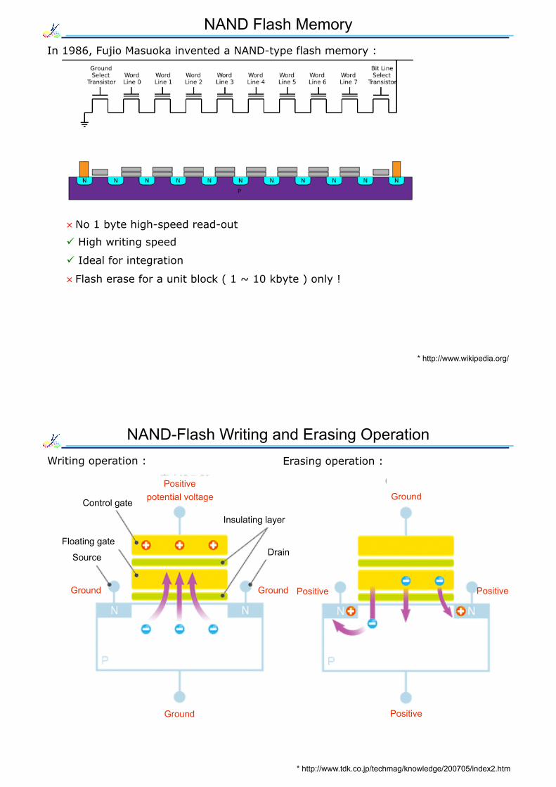
NAND-Flash Writing and Erasing Operation Writing operation : Erasing operation :
* http://www.tdk.co.jp/techmag/knowledge/200705/index2.htm
Positive potential voltage
Ground Ground
Control gate
Floating gate
Source
Insulating layer
Drain
Ground
Positive
Ground
Positive
Positive
13/11/14
3
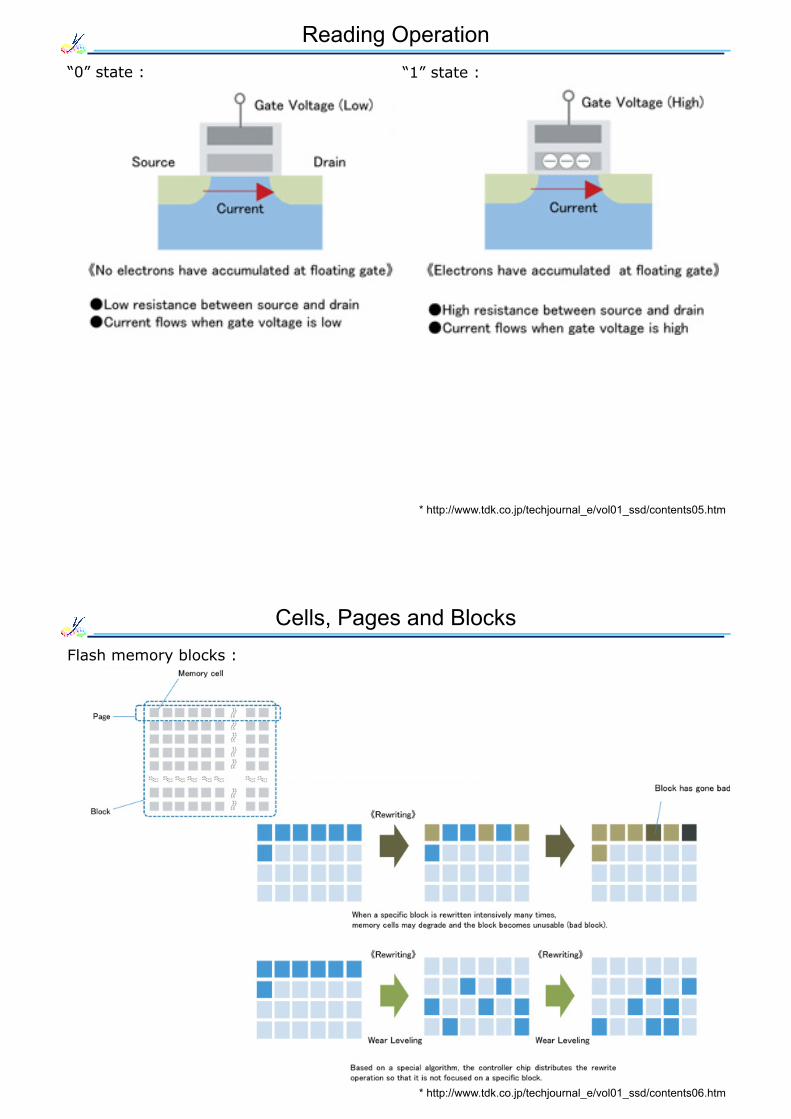
Reading Operation “0” state : “1” state :
* http://www.tdk.co.jp/techjournal_e/vol01_ssd/contents05.htm
Cells, Pages and Blocks Flash memory blocks :
* http://www.tdk.co.jp/techjournal_e/vol01_ssd/contents06.htm
13/11/14
4
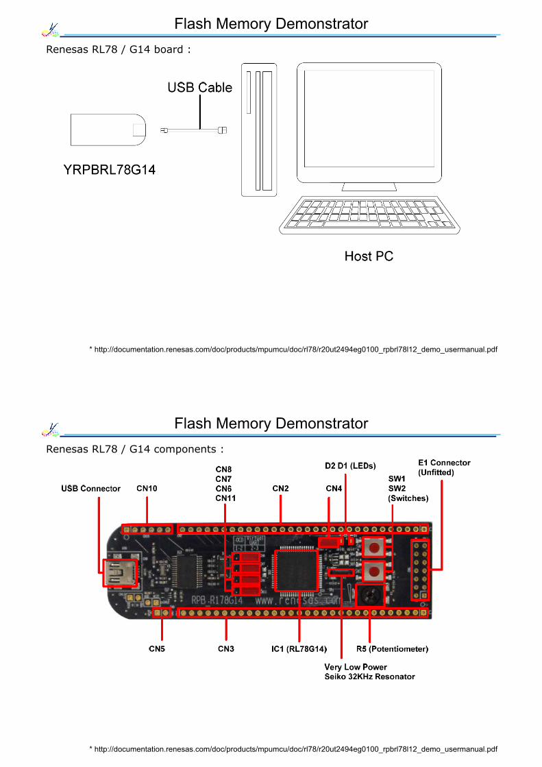
Flash Memory Demonstrator Renesas RL78 / G14 board :
* http://documentation.renesas.com/doc/products/mpumcu/doc/rl78/r20ut2494eg0100_rpbrl78l12_demo_usermanual.pdf
Flash Memory Demonstrator Renesas RL78 / G14 components :
* http://documentation.renesas.com/doc/products/mpumcu/doc/rl78/r20ut2494eg0100_rpbrl78l12_demo_usermanual.pdf

13/11/14
5
Getting Started Refer to Chapter 4 in the Manual :
* http://documentation.renesas.com/doc/products/mpumcu/doc/rl78/r20ut2494eg0100_rpbrl78l12_demo_usermanual.pdf
• Software installation (see Chapter 6)
• Software operation (Chapter 8)
• Analogue / digital converter demonstration (Section 8.3)
• Real time clock demonstration (Section 8.4)
→ Familiarise yourselves to the fundamental board operation.
• Memory demonstration (Section 8.5)
→ Learn writing operation into the flash memory.
• Low power demonstration (Section 8.6)
→ Learn low power consumption.
Discussion :
• Summarise the fundamental board operation.
• Summarise and discuss the writing operation.
• Compare the temperatures between the normal and low-power operation modes.
Flash Memory Evaluation Download CrystalDiskMark <http://crystalmark.info/?lang=en> :
* http://crystalmark.info/?lang=en
Discussion :
• Measure read / write speed of your own flash memory drives.
• Compare the above speed with those for USB 1.0 ~ 3.0.
• Discuss the development of the flash storages.
• Software installation
• Software operation (Chapter 8)
• http://crystalmark.info/software/CrystalDiskMark/manual-en/MainWindow.html