
Nanostructured Transition Metal Chalcogenides as Materials in


Advanced Electrode Materials

Scrivener Publishing100 Cummings Center, Suite 541J
Beverly, MA 01915-6106
Advanced Materials SeriesThe Advanced Materials Series provides recent advancements of the fascinating
field of advanced materials science and technology, particularly in the area of structure, synthesis and processing, characterization, advanced-state properties,
and applications. The volumes will cover theoretical and experimental approaches of molecular device materials, biomimetic materials, hybrid-type
composite materials, functionalized polymers, supramolecular systems, information- and energy-transfer materials, biobased and biodegradable or environmental friendly materials. Each volume will be devoted to one broad
subject and the multidisciplinary aspects will be drawn out in full.
Series Editor: Ashutosh TiwariBiosensors and Bioelectronics Centre
Linköping UniversitySE-581 83 Linköping
SwedenE-mail: [email protected]
Managing Editors: Sachin Mishra and Sophie Thompson
Publishers at ScrivenerMartin Scrivener ([email protected])
Phillip Carmical ([email protected])

Advanced Electrode Materials
Edited by
Ashutosh Tiwari, Filiz Kuralay and Lokman Uzun

Copyright © 2017 by Scrivener Publishing LLC. All rights reserved.
Co-published by John Wiley & Sons, Inc. Hoboken, New Jersey, and Scrivener Publishing LLC, Beverly, Massachusetts.Published simultaneously in Canada.
No part of this publication may be reproduced, stored in a retrieval system, or transmitted in any form or by any means, electronic, mechanical, photocopying, recording, scanning, or other wise, except as permit-ted under Section 107 or 108 of the 1976 United States Copyright Act, without either the prior writ-ten permission of the Publisher, or authorization through payment of the appropriate per-copy fee to the Copyright Clearance Center, Inc., 222 Rosewood Drive, Danvers, MA 01923, (978) 750-8400, fax (978) 750-4470, or on the web at www.copyright.com. Requests to the Publisher for permission should be addressed to the Permissions Department, John Wiley & Sons, Inc., 111 River Street, Hoboken, NJ 07030, (201) 748-6011, fax (201) 748-6008, or online at http://www.wiley.com/go/permission.
Limit of Liability/Disclaimer of Warranty: While the publisher and author have used their best efforts in preparing this book, they make no representations or warranties with respect to the accuracy or completeness of the contents of this book and specifically disclaim any implied warranties of merchant-ability or fitness for a particular purpose. No warranty may be created or extended by sales representa-tives or written sales materials. The advice and strategies contained herein may not be suitable for your situation. You should consult with a professional where appropriate. Neither the publisher nor author shall be liable for any loss of profit or any other commercial damages, including but not limited to spe-cial, incidental, consequential, or other damages.
For general information on our other products and services or for technical support, please contact our Customer Care Department within the United States at (800) 762-2974, outside the United States at (317) 572-3993 or fax (317) 572-4002.
Wiley also publishes its books in a variety of electronic formats. Some content that appears in print may not be available in electronic formats. For more information about Wiley products, visit our web site at www.wiley.com.
For more information about Scrivener products please visit www.scrivenerpublishing.com.
Cover design by Russell Richardson
Library of Congr ess Cataloging-in-Publication Data:
ISBN 978-1-119-24252-9
Printed in the United States of America
10 9 8 7 6 5 4 3 2 1
v
Contents
Preface xv
Part 1 State-of-the-Art Electrode Materials
1 Advances in Electrode Materials 3J. Sołoducho, J. Cabaj and D. Zając1.1 Advanced Electrode Materials for
Molecular Electrochemistry 41.1.1 Graphite and Related sp2-Hybridized
Carbon Materials 41.1.2 Graphene 6
1.1.2.1 Graphene Preparation 61.1.2.2 Engineering of Graphene 7
1.1.3 Carbon Nanotubes 81.1.3.1 Carbon Nanotube Networks for
Applications in Flexible Electronics 91.1.4 Surface Structure of Carbon Electrode Materials 11
1.2 Electrode Materials for Electrochemical Capacitors 121.2.1 Carbon-based Electrodes 121.2.2 Metal Oxide Composite Electrodes 131.2.3 Conductive Polymers-based Electrodes 151.2.4 Nanocomposites-based Electrode Materials for
Supercapacitor 161.3 Nanostructure Electrode Materials for Electrochemical
Energy Storage and Conversion 161.3.1 Assembly and Properties of Nanoparticles 17
1.4 Progress and Perspective of Advanced Electrode Materials 18
Acknowledgments 19References 19

vi Contents
2 Diamond-based Electrodes 27Emanuela Tamburri and Maria Letizia Terranova2.1 Introduction 272.2 Techniques for Preparation of Diamond Layers 28
2.2.1 HF-CVD Diamond Synthesis 302.2.2 MW-CVD Diamond Synthesis 312.2.3 RF-CVD Diamond Synthesis 31
2.3 Why Diamond for Electrodes? 322.4 Diamond Doping 33
2.4.1 In Situ Diamond Doping 342.4.2 Ion Implantation 37
2.5 Electrochemical Properties of Doped Diamonds 372.6 Diamond Electrodes Applications 39
2.6.1 Water Treatment and Disinfection 392.6.2 Electroanalytical Sensors 402.6.3 Energy Technology 45
2.6.3.1 Supercapacitors 452.6.3.2 Li Ion Batteries 492.6.3.3 Fuel Cells 51
2.7 Conclusions 52References 53
3 Recent Advances in Tungsten Oxide/Conducting Polymer Hybrid Assemblies for Electrochromic Applications 61Cigdem Dulgerbaki and Aysegul Uygun Oksuz3.1 Introduction 623.2 History and Technology of Electrochromics 633.3 Electrochromic Devices 63
3.3.1 Electrochromic Contrast 643.3.2 Coloration Efficiency 643.3.3 Switching Speed 653.3.4 Stability 653.3.5 Optical Memory 65
3.4 Transition Metal Oxides 673.5 Tungsten Oxide 673.6 Conjugated Organic Polymers 693.7 Hybrid Materials 703.8 Electrochromic Tungsten Oxide/Conducting
Polymer Hybrids 713.9 Conclusions and Perspectives 95Acknowledgments 99References 99

Contents vii
4 Advanced Surfactant-free Nanomaterials for Electrochemical Energy Conversion Systems: From Electrocatalysis to Bionanotechnology 103Yaovi Holade, Teko W. Napporn and Kouakou B. Kokoh4.1 Advanced Electrode Materials Design: Preparation and
Characterization of Metal Nanoparticles 1044.1.1 Current Strategies for Metal Nanoparticles
Preparation: General Consideration 1044.1.2 Emerged Synthetic Methods without Organic
Molecules as Surfactants 1094.2 Electrocatalytic Performances Toward Organic
Molecules Oxidation 1144.2.1 Electrocatalytic Properties of Metal Nanoparticles
in Alkaline Medium 1144.2.1.1 Electrocatalytic Properties Toward
Glycerol Oxidation 1144.2.1.2 Electrocatalytic Properties Toward
Carbohydrates Oxidation 1164.2.2 Spectroelectrochemical Characterization of the
Electrode–Electrolyte Interface 1184.2.2.1 Spectroelectrochemical Probing of
Electrode Materials Surface by CO Stripping 118
4.2.2.2 Spectroelectrochemical Probing of Glycerol Electrooxidation Reaction 120
4.2.2.3 Spectroelectrochemical Probing of Glucose Electrooxidation Reaction 121
4.2.3 Electrochemical Synthesis of Sustainable Chemicals: Electroanalytical Study 123
4.2.4 Electrochemical Energy Conversion: Direct Carbohydrates Alkaline Fuel Cells 128
4.3 Metal Nanoparticles at Work in Bionanotechnology 1314.3.1 Metal Nanoparticles at Work in Closed-biological
Conditions: Toward Implantable Devices 1314.3.2 Activation of Implantable Biomedical and
Information Processing Devices by Fuel Cells 1334.4 Conclusions 136Acknowledgments 137Notes 137References 138

viii Contents
Part 2 Engineering of Applied Electrode Materials
5 Polyoxometalate-based Modified Electrodes for Electrocatalysis: From Molecule Sensing to Renewable Energy-related Applications 149Cristina Freire, Diana M. Fernandes, Marta Nunes and Mariana Araújo5.1 Introduction 1505.2 POMs and POMs-based (Nano)Composites 151
5.2.1 Polyoxometalates 1515.2.2 Polyoxometalate-based (Nano)Composites 1545.2.3 General Electrochemical Behavior of POMs 157
5.3 POMs-based Electrocatalysis for Sensing Applications 1605.3.1 Reductive Electrocatalysis 161
5.3.1.1 Nitrite Reduction 1615.3.1.2 Bromate Reduction 1675.3.1.3 Iodate Reduction 1685.3.1.4 Hydrogen Peroxide Reduction Reaction 170
5.3.2 Oxidative Electrocatalysis 1735.3.2.1 Dopamine and Ascorbic Acid Oxidations 1735.3.2.2 l-Cysteine Oxidation 177
5.4 POMs-based Electrocatalysis for Energy Storage and Conversion Applications 1785.4.1 Oxygen Evolution Reaction 1795.4.2 Hydrogen Evolution Reaction 1835.4.3 Oxygen Reduction Reaction 185
5.5 Concluding Remarks 191Acknowledgments 193List of Abbreviations and Acronyms 193References 196
6 Electrochemical Sensors Based on Ordered Mesoporous Carbons 213Xiangjie Bo and Ming Zhou6.1 Introduction 2136.2 Electrochemical Sensors Based on OMCs 2176.3 Electrochemical Sensors Based on Redox
Mediators/OMCs 2226.4 Electrochemical Sensors Based on NPs/OMCs 226
6.4.1 Electrochemical Sensors Based on Transition Metal NPs/OMCs 228

Contents ix
6.4.2 Electrochemical Sensors Based on Noble Metal NPs/OMCs 230
6.5 Conclusions 233Acknowledgments 236References 236
7 Non-precious Metal Oxide and Metal-free Catalysts for Energy Storage and Conversion 243Tahereh Jafari, Andrew G. Meguerdichian, Ting Jiang, Abdelhamid El-Sawy and Steven L. Suib7.1 Metal–Nitrogen–Carbon (M–N–C) Electrocatalysts 244
7.1.1 Introduction 2447.1.2 Catalysts for Hydrogen Evolution Reaction 2457.1.3 Catalysts for Oxygen Evolution Reaction 2487.1.4 Catalysts for Oxygen Reduction Reaction 2497.1.5 None-heat-treated M–N–C Electrocatalysts 2507.1.6 Heat-treated M–N–C Electrocatalysts 2547.1.7 Conclusion 261
7.2 Transition Metal Oxide Electrode Materials for Oxygen Evolution Reaction, Oxygen Reduction Reaction and Bifuctional Purposes (OER/ORR) 2627.2.1 Introduction 2627.2.2 Oxygen Evolution Reaction 266
7.2.2.1 Synthesis Methodology 2677.2.2.2 OER Properties of Catalyst 2727.2.2.3 Morphology or Microstructure Analysis
of TM Oxide for OER 2747.2.3 Oxygen Reduction Reaction 276
7.2.3.1 Morphology or Microstructure Analysis 2777.2.3.2 ORR Properties of Catalyst 2787.2.3.3 Synthesis Methodology 2787.2.3.4 Theoretical Analyses of ORR Active
Catalysts 2797.2.4 Hydrogen Evolution Reaction 2797.2.5 Bifunctional Oxide Materials (OER/ORR) 281
7.2.5.1 Bifunctional Properties of Catalyst 2817.2.5.2 Dopant Effects 2837.2.5.3 Morphology or Microstructure Analysis 2837.2.5.4 Synthesis Methodology 284
7.2.6 Conclusion 285

x Contents
7.3 Transition Metal Chalcogenides, Nitrides, Oxynitrides, and Carbides 2857.3.1 Transition Metal Chalcogenides 2857.3.2 Transition Metal Nitrides 2947.3.3 Transition Metal Oxynitrides 2967.3.4 Transition Metal Carbides 298
7.4 Oxygen Reduction Reaction for Metal-free 3007.4.1 Different Doping Synthesis Strategies 3007.4.2 ORR Activity in Different Carbon Source 303
7.4.2.1 1D Carbon Nanotube Doped 3037.4.2.2 2D Graphene 306
7.4.3 Oxygen Evolution Reaction 308References 310
8 Study of Phosphate Polyanion Electrodes and Their Performance with Glassy Electrolytes: Potential Application in Lithium Ion Solid-state Batteries 321S. Terny and M.A. Frechero8.1 Introduction 3218.2 Glass Samples Preparation 3238.3 Nanostructured Composites Sample Preparation 3248.4 X-ray Powder Diffraction 325
8.4.1 X-ray Powder Diffraction Patterns of Glassy Materials 325
8.4.2 X-ray Powder Diffraction Patterns of Composites Materials 326
8.5 Thermal Analysis 3268.5.1 Thermal Analysis of Glassy Systems 3268.5.2 Thermal Analysis of Nanocomposites Materials 329
8.6 Density and Appearance 3308.6.1 Density and Oxygen Packing Density of Glassy
Materials 3308.6.2 Materials’ Appearance 331
8.6.2.1 Glasses 3318.6.2.2 Nanostructured Composites 332
8.7 Structural Features 3328.7.1 Glassy Materials 332
8.7.1.1 FTIR and Raman Spectroscopy 3348.7.2 Nanocomposites Materials 337
8.8 Electrical Behavior 3428.8.1 Glasses Materials 3428.8.2 Composite Materials 347
Contents xi
8.9 All-solid-state Lithium Ion Battery 3498.10 Final Remarks 350Acknowledgments 352References 352
9 Conducting Polymer-based Hybrid Nanocomposites as Promising Electrode Materials for Lithium Batteries 355O.Yu. Posudievsky, O.A. Kozarenko, V.G. Koshechko and V.D. Pokhodenko9.1 Introduction 3569.2 Electrode Materials of Lithium Batteries Based on
Conducting Polymer-based Nanocomposites Prepared by Chemical and Electrochemical Methods 3579.2.1 Host–guest Hybrid Nanocomposites 3579.2.2 Core–shell Hybrid Nanocomposites 361
9.3 Mechanochemical Preparation of Conducting Polymer-based Hybrid Nanocomposites as Electrode Materials of Lithium Batteries 3689.3.1 Principle of Mechanochemical Synthesis 3689.3.2 Mechanochemically Prepared Conducting
Polymer-based Hybrid Nanocomposite Materials for Lithium Batteries 370
9.4 Conclusion 384References 385
10 Energy Applications: Fuel Cells 397Mutlu Sönmez Çelebi10.1 Introduction 39810.2 Catalyst Supports for Fuel Cell Electrodes 399
10.2.1 Commercial Carbon Supports 399 10.2.2 Carbon Nanotube (CNT) Supports 401 10.2.3 Graphene Supports 403 10.2.4 Mesoporous Carbon Supports 405 10.2.5 Other Carbon Supports 406 10.2.6 Conducting Polymer Supports 408 10.2.7 Hybrid Supports 410 10.2.8 Non-carbon Supports 411
10.3 Anode and Cathode Catalysts for Fuel Cells 413 10.3.1 Anode Catalysts 413 10.3.2 Cathode Catalysts 418
10.4 Conclusions 420References 421

xii Contents
11 Novel Photoelectrocatalytic Electrodes Materials for Fuel Cell Reactions 435Mingshan Zhu, Chunyang Zhai and Cheng Lu11.1 Introduction 43511.2 Basic Understanding on the Improved
Catalytic Performance of Photo-responsive Metal/Semiconductor Electrodes 438
11.3 Synthetic Methods for Metal/Semiconductor Electrodes 440
11.3.1 Electrochemical Deposition 441 11.3.2 Chemical Reduction Method 442 11.3.3 Physical Mixing Method 443 11.3.4 Hydrothermal/Solvothermal Method 444 11.3.5 Microwave-assisted Method 445 11.3.6 Other Preparation Methods 445
11.4 Photo-responsive Metal/Semiconductor Anode Catalysts 446
11.4.1 TiO2 Nanoparticles 446 11.4.2 One-dimensional Well-aligned TiO2
Nanotube Arrays 448 11.4.3 Other Semiconductor Supports 449
11.5 Conclusions and Future Outlook 452References 453
12 Advanced Nanomaterials for the Design and Construction of Anode for Microbial Fuel Cells 457Lu Bai, Ming Zhou and Chaokang Gu12.1 Introduction 45812.2 Carbon Nanotubes-based Anode Materials for MFCs 45912.3 Graphene-based Anode Materials for MFCs 46612.4 Other Anode Materials for MFCs 47012.5 Conclusions 474Acknowledgments 475References 475
13 Conducting Polymer-based Electrochemical DNA Biosensing 485Filiz Kuralay13.1 Introduction 48613.2 Electrochemical DNA Biosensors 487

Contents xiii
13.3 Conducting Polymer-based Electrochemical DNA Biosensors 489
13.4 Conclusions and Outlook 493Acknowledgments 494References 494
Index 501


Preface
Among the hot topics concerning advanced materials are recent advances in electrode materials because of their importance not only in developing new biosensors but also in designing efficient batteries, fuel cells and, of course, energy storage and conversion systems. Therefore, we have tried to compile various valuable aspects of this hot topic as a part of the Advanced Materials Series.
In this book, a narrative is presented of recent advances in electrode materials and their novel applications, which are a cross section of advanced materials. Electrochemistry is a widely used branch of chemistry which combines chemical and electrical effects. It provides the advantages of high sensitivity, high performance and low cost. In electrochemistry, a well-designed electrode material is the key to many applications. Therefore, we have summarized different electrodes used in various fields for enhancing the quality of electrochemical systems. We begin with a chapter regarding advances in electrode materials, particularly those based on energy stor-age, since an electrode is one of the important parts of electrochemical capacitors as well as energy storage and conversion products. The major classes of suitable electrode materials used for capacitors are commonly activated nanoporous carbon, graphene, carbon nanotubes, conducting polymers, metal oxides and polymer composites, which have been exten-sively reported on in the literature.
Diamond-based electrodes have garnered great attention for use in electrochemical systems. Therefore, detailed techniques used in chemical vapor deposition (CVD) to generate polycrystalline and nanocrystalline diamond layers are also covered, along with methodologies employed to dope the diamond phase in order to obtain an electrically conductive mate-rial. Then, the use of diamond-based layers for the assembly of electrodes is summarized to inform readers in areas related to the environment and renewable energies, including food and pharmaceutical analysis, soil and water purification, supercapacitors, Li-ion cells and fuel cells. Recent advances in tungsten oxide/conducting polymer hybrid assemblies for elec-trochromic applications have taken place which emphasize the importance
xv

xvi Preface
of developing new technologies that can be used for electrochromic appli-cations. Tungsten oxide (WO3) has emerged as one of the key materials for electrochromic devices since it exhibits the best electrochromic activ-ity among transition metal oxides. The introduction of WO3/ conducting polymer-based hybrid materials has prompted the development of nano-composites with properties unmatched by conventional counterparts. The interdisciplinary research involving materials science, bioelectrochemis-try and electrochemistry is still the hallmark of many technological and fundamental breakthroughs. The effectiveness of surfactant-free metal nanoparticles as “abiotic” catalysts in biotechnology are outlined, based on systems harvesting energy from biological sources for various sensing and wireless information-processing devices for biomedical, homeland and environmental monitoring applications. In another chapter, polyoxometa-lates (POMs) based on concepts of biosensors for renewable energy appli-cations are summarized. POMs are a well-known class of discrete early transition metal-oxide clusters with a variety of sizes, shapes, compositions and physical and chemical properties, which undergo reversible multiva-lence reductions/oxidations. Electrochemical sensors based on ordered mesoporous carbons are also highlighted since they provide high sensitiv-ity and selectivity.
Conducting polymer-based electrochemical DNA biosensing is also detailed in the book. Electrode materials for fuel cells lead to important reactions such as oxygen evolution reactions (OER), hydrogen evolution reactions (HER), and oxygen reduction reactions (ORR). In metal-air bat-teries and fuel cells, the most sluggish reaction is the ORR reaction, which is the bottleneck of numerous electrochemical reactions. Key electrocata-lytic reactions occur at the cathode of a proton exchange membrane fuel cell (PEMFC). Therefore, inexpensive materials that have high activity, sta-bility, and resistance to methanol crossover effects for ORR-HOR and OER reactions have been summarized in one of the chapters. In another chap-ter, a study of phosphate polyanion electrodes and their performance with glassy electrodes for potential application in lithium-ion solid-state batter-ies is presented in order to stress the importance of new generation solid-state batteries. Then, in a related area, conducting polymer-based hybrid nanocomposites for lithium batteries are given. In this chapter, host-guest and core-shell hybrid nanocomposites based on conducting conjugated polymers and inorganic compounds, which are considered active compo-nents of the lithium batteries, are reported. Later on, electrode materials for fuel cell applications are categorized and evaluated in two separate parts as catalyst supports and anode/cathode catalysts. Platinum (Pt)-based cata-lysts make fuel cell technology less cost-effective due to the limited supply

Preface xvii
and high cost of Pt. Thus, research on the cost reduction of fuel cells is dealt with either by optimization of existing Pt catalysts or development of Pt or non-Pt alloy catalysts with new and improved electronic structures. Novel photoelectrocatalytic electrode materials for fuel cell reactions are also summarized, with the main focus of the chapter being the recent progress of novel photoresponsive electrodes as anode catalysts for improving the photoelectrocatalytic activity of low molecular weight alcohols oxidation under light irradiation. Finally, advanced nanomaterials for the design and construction of anode materials for microbial cells are detailed at the end of the book.
The invaluable efforts of distinguished researchers from ten different countries with seventeen different affiliations have helped build a com-prehensive book from the perspective of advanced materials. By including information presented by such a wide range of authors we hope to contrib-ute to the understanding of students and researchers as well as industrial partners from different fields.
Editors AshutoshTiwari, PhD, DSc
Filiz Kuralay, PhDLokman Uzun, PhD
September 2016


Part 1STATE-OF-THE-ART ELECTRODE
MATERIALS


3
Ashutosh Tiwari, Filiz Kuralay and Lokman Uzun (eds.) Advanced Electrode Materials, (3–26) © 2017 Scrivener Publishing LLC
1
Advances in Electrode MaterialsJ. Sołoducho*, J. Cabaj and D. Zając
Faculty of Chemistry, Wroclaw University of Science and Technology, Wrocław, Poland
AbstractElectrode is the key part of the electrochemical capacitors (also known as supercapacitors) as well as energy storage and conversion products or other electrochemical devices, so the electrode materials are the most important factors to determine the properties of these tools. The major classes of suitable electrode materials used for the capacitors as well as an energy storage and conversion materials or other electrochemical devices are activated nanoporous carbon, graphene, carbon nanotubes, conducting polymers, metal oxides, and polymer composites, which have been extensively reported in the literature. In addition, the wellknown applications of advanced electrodes in metals production, energy storage in batteries and supercapacitors, and catalyst supports have appeared in the literature on both carbon materials and their interactions with electrolytes and redox systems. Since the significant application of graphite electrodes for electrochemical production of alkali metals, carbon materials have been broadly used in both analytical and industrial electrochemistry. The oftencited benefits of carbon electrodes contain reasonable cost, wide potential window, relatively inert electrochemistry, and electrocatalytic activity for a variety of redox reactions. Energy storage techniques appear as one of the most promising options in harvesting renewably generated energy during the optimum manufacture period for future use. Of the available electrical energy storage devices, fuel cells, batteries, and capacitors have been the technology of choice for most applications. Herein, the storage principles and characteristics of electrode materials, including carbonbased materials, transition metal oxides, and conductive polymers for advanced electrodes are depicted briefly.
Keywords: Electrode material, semiconductors, carbon materials, electrochemistry, conducting polymers
*Corresponding author: [email protected]

4 Advanced Electrode Materials
1.1 Advanced Electrode Materials for Molecular Electrochemistry
Regardless of extensive developments of carbon materials for electrochemistry, recent years have brought essential novelties that impart the significance to the utility of the material in organic and biological electrochemistry. Fullerenes, vapordeposited carbon films, and microfabricated carbon structures tender features compared with the graphitic carbon electrodes in universal use in the early 1990s and also enable modern adoptions in electronics, sensing, as well as electrocatalysis [1].
Due to the facts, nanocarbon is believed to play a crucial role. Carbon nanoscience brings promise for an evolution in electronics in the future. Three important elements make sp2 carbon particular for facing the nanochallenges. First is the strong covalent sp2 bonding between atoms, next are the enlarged electron clouds coming from the pz orbitals, and third is the simplicity of the sp2 carbon system [2].
1.1.1 Graphite and Related sp2-Hybridized Carbon Materials
The energy difference between the 2s and 2p orbitals is less than the energy gain, through C–C bond. Due to the fact, when carbon atoms bind to each other, their 2s and 2p orbitals can mix. To generate the diamond structure, the orbitals for one 2s and three 2p electrons mix, creating four sp3 orbitals (regular tetrahedron). In comparison, in the sp2 configuration, the 2s and two 2p orbitals mix to generate three inplane covalent bonds. In this situation, each C atom has three nearest neighbors, creating the hexagonal planar network of graphene. At last, the sp hybridization, mixing the orbitals of only one 2s and one 2p electron is also possible, and it gives rise to linear chains of carbon atoms, the basis for polyene, the filling of the stem of certain nanotubes [3], and providing a step in the coalescence of adjacent nanotubes [4].
The idea of sp2 nanocarbons begins with the single graphene sheet (Figure 1.1), the planar lattice of sp2hybridized carbon atoms. The system can be large in the plane, and it is only one atom thick, thus representing a twodimensional sp2 nanocarbon [2].
Threedimensional (3D) graphite is one of the bestknown/investigated forms of pure carbon, being found as a natural source (mineral). Of all materials, graphite possesses the highest melting point (4200 K), the highest thermal conductivity (3000 W/mK), and a highroomtemperature electron mobility (30 000 cm2/Vs) [5]. Synthetic graphite was developed in 1960 by Arthur Moore [2] and was named highly oriented pyrolytic

Advances in Electrode Materials 5
Figure 1.1 Structures of sp2 carbon materials, including (a) singlelayer, (b) a singlewall carbon nanotube (SWCNT), and (c) a C60 fullerene.
(a) (b) (c)
Table 1.1 Applications of traditional graphitebased materials including carbon fibers [6].
Traditional graphite materials Commercial applications
Graphite and graphitebased products
Materialsprocessing applications such as furnaces/crucibles, large electrodes in metallurgical processes, electrical, and electronic devices such as electric brushes, membrane switches, variable resistors, etc.
Electrochemical applications for electrode materials in primary and secondary batteries, separators for fuel cells, nuclear fission reactors, bearings and seals (mechanical), and dispersions such as inks.
Carbonfiberbased products
Carbonfiber composites aerospace (70%), sporting goods (18%), industrial equipment (7%), marine (2%), and miscellaneous (3%).
Carbon–carbon composites
Hightemperature structural materials, aerospace applications, such as missile nose tips, reentry heat shields, etc. brakedisc applications (lightweight, high thermal conductivity, stability), rotating shafts, pistons, bearings (low coefficient of friction), biomedical implants such as bone plates (biocompatibility).
graphite. Graphite and its related carbon fibers [2] have been utilized commercially for decades [6]. Their utility ranges from a conductive fillers and mechanical structural reinforcements in composites to electrode materials exploiting their resiliency (Table 1.1) [6].

6 Advanced Electrode Materials
1.1.2 Graphene
Graphene is an encouraging newgeneration conducting material with the potential to displace customary electrode (i.e. indium tin oxide) in electrical and optical devices. It combines several advantageous features containing low sheet resistance, high optical transparency, and splendid mechanical properties. Recent study has concurred with growing interest in the application of graphene as an electrode material in transistors, lightemitting diodes, solar cells, and flexible devices.
Since discovered, graphene has attracted interest due to its benefits such as high charge mobility, transparency, mechanical strength, and flexibility [7]. Due to the fact, graphene is supposed to play a vital role as a transparent electrode in electronic and optoelectronic devices [7]. Transparent electrodes are a significant element of a number of devices, such as displays (liquid crystal displays, cellular phones, epaper), lightemitting diodes, and photovoltaic devices. Among these, graphene is significantly interesting because it has been successfully synthesized on a large scale as a good conducting and transferable film [7].
1.1.2.1 Graphene Preparation
Graphene has been produced by several methods (which were well reviewed by Jo et al. [7]), including:
a. precipitation on a silicon carbide surface [8],b. mechanical exfoliation from graphite [9],c. chemically converted graphene from solutionphase graphene
oxide [10], d. growth by chemical vapor deposition (CVD) on catalytic
metal surfaces [11].
The size and character of a graphene film depend on the technique used for its fabrication. Berger et al. reported the heat treatment of SiC in a vacuum or in an inert environment to generate a graphene layer on the SiC surface [12], which is a result of the evaporation of silicon atoms from the SiC surface and the resultant segregation of carbon atoms on the surface. It was expected that this procedure would be appropriate for the fabrication of highquality graphene; but, the size of a single domain of the layer thickness has not overstepped a few micrometers. There was also reported the successful isolation of graphene by mechanical exfoliation with Scotch tape [9]. This exfoliation method will remain the method of choice for fabricating proofofconcept devices [13].

Advances in Electrode Materials 7
In 2006, Stankovich et al. reported a solutionbased process for producing singlelayer graphene [14]. After oxidation by Hummers’ method, graphene oxide becomes a layered stack of puckered sheets with AB stacking [15]. Graphene oxide itself is not conducting, but the graphitic network can be substantially restored by thermal annealing or through treatment with chemical reducing agents. Moreover, electrical enhancement of reduced graphene oxide layer may be achieved by doping process and/or a hybrid approach with other conducting elements such as carbon nanotubes (CNTs) [16] and metal grids [17].
Precipitation on a silicon carbide surface and mechanical exfoliation techniques are not suitable for largescale fabrication of devices. In comparison, chemically converted graphene from solutionphase graphene oxide and CVDgrown graphene layers permit largescale graphene integration with other materials [18, 19].
1.1.2.2 Engineering of Graphene
High conductivity and low optical absorption execute graphene an extremely inviting material for a transparent conducting electrode. Graphene layers that have high conductivity and low optical loss can be modified to achieve i.e. doped graphene films and/or grapheme electrodes.
The usefulness of graphene in applications such as electrodes is widely directed by two crucial factors: (1) sheet resistance and (2) visiblelight transmission. The sheet resistance is lowered as the graphene layer becomes thicker, but the transmission is also decreased as the thickness grows up. An appropriate transparent conductor should be characterized with high electrical conductivity connected with low absorption of visible light [7].
To improve the conducting properties of graphene, the charge concentration of the carbon film has to be adjusted by shifting the Fermi level of graphene’s zerogap band structure away from the Dirac point, where the density of states is zero [20]. The required stiff band shift may be prompted by chemical doping [20], electrostatic gating [21], a metal contact [22], or dipole formation [23]. In example, hole (p) or electron (n) doping can be observed by utilization of elements as B or N [24], which can be immediately substituted into the carbon grate [25]. The nitrogen species in Ndoped graphene are pyridinic N and pyrrolic N, which are generated predominately by substituting a carbon atom with nitrogen along inplane edge or defect sites because such carbon atoms are more chemically active than those within the lattice of perfect graphene. Alike, in a Bdoped graphene grate are met by a B–C bond and B–O bond.

8 Advanced Electrode Materials
Graphene may also be doped through the adsorption of chemical species on its surface, i.e. by immersing graphene layers in AuCl3 solution [26]. HNO3 is another example of an adsorbate that can be utilized to pdope graphene lattices [27]. In fact, the modification of sheet resistance and work function by doping process is valid in enhancing the performance and efficiency of different electrical and optical devices based on graphene electrodes.
1.1.3 Carbon Nanotubes
A SWCNT (Figure 1.1) can be imagined as a cylinder generate by rolling up a graphene sheet along a vector Ch = na1 + ma2, where a1 and a2 are the basis vectors of the hexagonal crystal lattice of graphene. The indexes (n, m) state the two integral parameters (diameter and chirality) of the nanotube.
The unusual structure–property attitude creates SWCNTs as a candidate for molecular electronic tools such as channel material for fieldeffect transistors (FETs) [28]. Moreover, a number of researches have already reported that SWCNTs exhibit interesting electronic properties, which are well outside their standard material counterparts, i.e. the charge transport capability of metallic SWCNTs can attain 109 A/cm2 (better than aluminum or copper), while semiconducting SWCNTs can achieve fieldeffect mobilities up to 104 cm2 V−1s−1 [29]. However, tools based on separate SWCNTs suffer from weak uniformity and reproducibility, mostly in order to hardness in solid synthesis of nanotubes with homogeneous structural advantages, as well as governable setup of SWCNTs over a large area [30]. Due to the fact, macroscale setups of SWCNTs, particularly random networks and thin layers, are seemed to enable the most truthful adoptions of nanotubes in molecular electronics in the short time since they tender not only convenient technology but also unitary and reproducible output [30]. Moreover, SWCNT networks are in particular adequate for flexible and stretchable electronic devices since the lateral deformation of the curvy and entangled SWCNTs may accommodate really large strains [31]. Truly, there have already been a number of reports demonstrating the valid promise of nanotube networks as the channel materials and/or electrodes in various types of flexible/stretchable electronic tools, such as integrated circuits [32], sensors [31], organic lightemitting diodes [33], supercapacitors [34], touch panels [35], and other.
Several methods are accessible to create CNT networks and thin films as presented in Figure 1.2. In general, they may be grouped into two classes: dry processes and solution ones [36]. Dry techniques are mostly direct
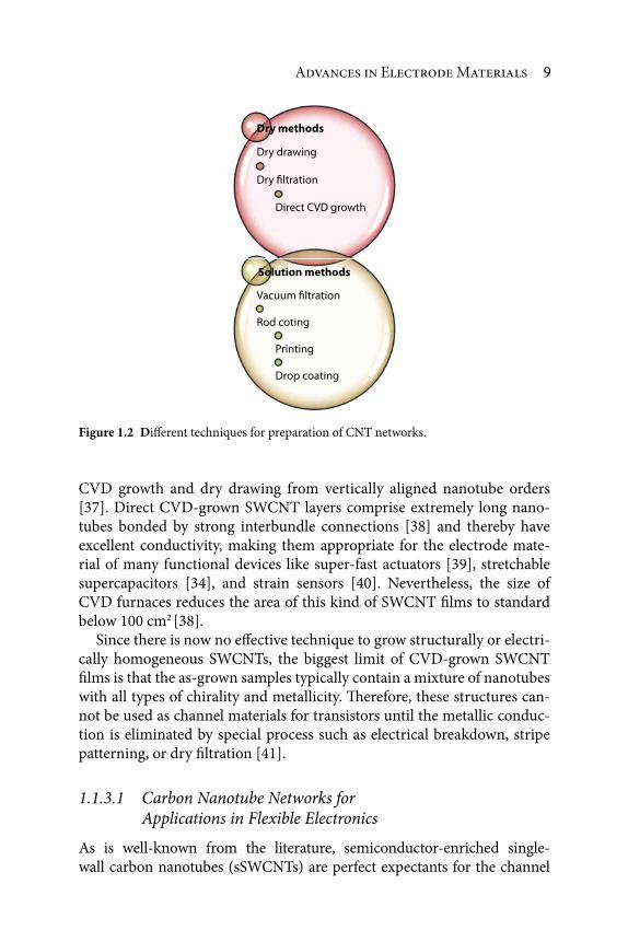
Advances in Electrode Materials 9
CVD growth and dry drawing from vertically aligned nanotube orders [37]. Direct CVDgrown SWCNT layers comprise extremely long nanotubes bonded by strong interbundle connections [38] and thereby have excellent conductivity, making them appropriate for the electrode material of many functional devices like superfast actuators [39], stretchable supercapacitors [34], and strain sensors [40]. Nevertheless, the size of CVD furnaces reduces the area of this kind of SWCNT films to standard below 100 cm2 [38].
Since there is now no effective technique to grow structurally or electrically homogeneous SWCNTs, the biggest limit of CVDgrown SWCNT films is that the asgrown samples typically contain a mixture of nanotubes with all types of chirality and metallicity. Therefore, these structures cannot be used as channel materials for transistors until the metallic conduction is eliminated by special process such as electrical breakdown, stripe patterning, or dry filtration [41].
1.1.3.1 Carbon Nanotube Networks for Applications in Flexible Electronics
As is wellknown from the literature, semiconductorenriched singlewall carbon nanotubes (sSWCNTs) are perfect expectants for the channel
Dry �ltration
Direct CVD growth
Solution methods
Vacuum �ltration
Rod coting
Printing
Drop coating
Dry methods
Dry drawing
Figure 1.2 Different techniques for preparation of CNT networks.

10 Advanced Electrode Materials
material of flexible thinfilm transistors (TFTs) due to the unexampled mixture of lowtemperature technology, mechanical facility, optical transparency, and unusual electrical character. By using highpurity sSWCNT solutions, Wang et al. fabricated waferscale nanotube networks with high density and uniformity [42], which in consequence provided the fabrication of TFTs and logical circuits on both rigid and flexible solids [43]. Due to the tradeoff between on/off ratio and transconductance, TFTs with wide channel lengths (high Ion/Ioff) are adequate for logical circuits, while the tools with short channel lengths (large gm) are appropriate for analog and radio frequency application. In addition, capacitance–voltage (C–V) measurements are performed to precisely determine the gate capacitance which in turn leads to an accurate assessment of the fieldeffect mobility (z), with a typical value of ~50 cm2 V−1 s−1 [43], similar to that of lowtemperature polysilicon and much higher than those of amorphous silicon and organic semiconductors. Moreover, the use of ultrathin polyimide solids results in highly flexible TFTs and integrated logical circuits, including inverter, NOR, and NAND gates. Such tools and circuits reveal sufficient stability after thousands of bending cycles. TFTs have also been incorporated into different functional systems, including sensors [44], displays [45], and electronic skins [46]. Substituting different type of sensors, such as chemical sensor, light sensor, and temperature sensor, for the pressure sensor could allow various functionalities of eskin or superior to natural skins and find a wide range of applications in smart robotics and security/healthmonitoring tools.
Huge progress has been observed recently in SWCNTbased flexible and stretchable electronics. Nevertheless, almost no SWCNTbased flexible product is commercially available at this moment [47]. A number of challenges remain to be conquered before SWCNTbased electronic tools and setups can be fabricated ready for the commercial applications.
In the material feature, while semiconductorenriched SWCNTs are already commercially available, there is still wide inhomogeneity in terms of chirality and nanotube length. It is clear that purity and sufficient homogeneity of the starting material is advantageous for steady tool performance. Moreover, long nanotubes are required to low the number of tubetotube junctions, which could lead to subsequent improvement in tool mobility. However, the dissolution and separation of long nanotubes (>10 μm) are not facile. Moreover, the effects of surfactants on tool electrical behaviors require more precise development. The surfactants used to disperse SWCNTs are hard to eliminate and can behave as obstacles for electronic conduction. Consequently, new surfactantfree procedures need to be investigated to effectively dissolve SWCNTs. Recent reports of


![Hydrogen-Evolution Catalysts Based on Non-Noble Metal ... · cial processes unattractive. Several non-noble metal materi-als, such as transition-metal chalcogenides,[2] carbides,[3]](https://static.fdocuments.net/doc/165x107/5d1f5e3088c993ce268cad2c/hydrogen-evolution-catalysts-based-on-non-noble-metal-cial-processes-unattractive.jpg)


![Nitrogen-rich transition metal nitrides - Eprints · PDF filecurrent knowledge of transition metal nitride-carbide ... [33] or radiofrequency sputtering ... There is a significant](https://static.fdocuments.net/doc/165x107/5aa4319d7f8b9ab4788b86b0/nitrogen-rich-transition-metal-nitrides-eprints-knowledge-of-transition-metal.jpg)


![Nitrogen-rich transition metal nitrides - Eprintseprints.soton.ac.uk/356185/1/356185.pdf · Nitrogen-rich transition metal nitrides Ashkan Salamat[a]*, Andrew L. Hector[b], Peter](https://static.fdocuments.net/doc/165x107/5af5ee5e7f8b9a9546900508/nitrogen-rich-transition-metal-nitrides-transition-metal-nitrides-ashkan-salamata.jpg)
