cryogenic deep reactive ion etching of silicon micro and - Aaltodoc
Upload
mehdi-naderiCategory
view
219download
0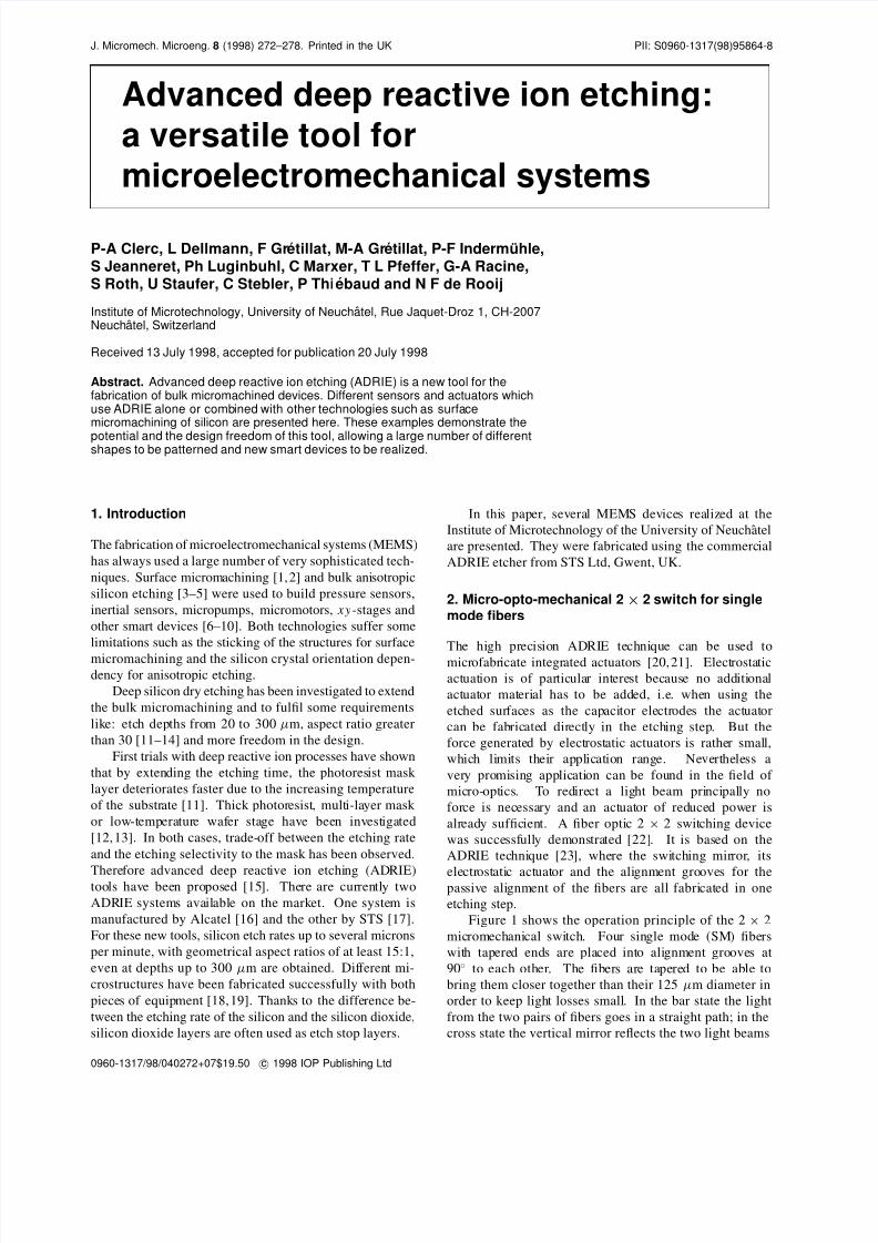
8/3/2019 Advanced deep reactive ion etching: a versatile tool for microelectromechanical systems
http://slidepdf.com/reader/full/advanced-deep-reactive-ion-etching-a-versatile-tool-for-microelectromechanical 1/7
J. Micromech. Microeng. 8 (1998) 272–278. Printed in the UK PII: S0960-1317(98)95864-8
Advanced deep reactive ion etching:a versatile tool formicroelectromechanical systems
P-A Clerc, L Dellmann, F Gretillat, M-A Gretillat, P-F Indermuhle,S Jeanneret, Ph Luginbuhl, C Marxer, T L Pfeffer, G-A Racine,S Roth, U Staufer, C Stebler, P Thiebaud and N F de Rooij
Institute of Microtechnology, University of Neuchatel, Rue Jaquet-Droz 1, CH-2007Neuchatel, Switzerland
Received 13 July 1998, accepted for publication 20 July 1998
Abstract. Advanced deep reactive ion etching (ADRIE) is a new tool for thefabrication of bulk micromachined devices. Different sensors and actuators whichuse ADRIE alone or combined with other technologies such as surfacemicromachining of silicon are presented here. These examples demonstrate the
potential and the design freedom of this tool, allowing a large number of differentshapes to be patterned and new smart devices to be realized.
1. Introduction
The fabrication of microelectromechanical systems (MEMS)
has always used a large number of very sophisticated tech-
niques. Surface micromachining [1, 2] and bulk anisotropic
silicon etching [3–5] were used to build pressure sensors,
inertial sensors, micropumps, micromotors, xy-stages and
other smart devices [6–10]. Both technologies suffer some
limitations such as the sticking of the structures for surface
micromachining and the silicon crystal orientation depen-dency for anisotropic etching.
Deep silicon dry etching has been investigated to extend
the bulk micromachining and to fulfil some requirements
like: etch depths from 20 to 300 µm, aspect ratio greater
than 30 [11–14] and more freedom in the design.
First trials with deep reactive ion processes have shown
that by extending the etching time, the photoresist mask
layer deteriorates faster due to the increasing temperature
of the substrate [11]. Thick photoresist, multi-layer mask
or low-temperature wafer stage have been investigated
[12, 13]. In both cases, trade-off between the etching rate
and the etching selectivity to the mask has been observed.
Therefore advanced deep reactive ion etching (ADRIE)tools have been proposed [15]. There are currently two
ADRIE systems available on the market. One system is
manufactured by Alcatel [16] and the other by STS [17].
For these new tools, silicon etch rates up to several microns
per minute, with geometrical aspect ratios of at least 15:1,
even at depths up to 300 µm are obtained. Different mi-
crostructures have been fabricated successfully with both
pieces of equipment [18, 19]. Thanks to the difference be-
tween the etching rate of the silicon and the silicon dioxide,
silicon dioxide layers are often used as etch stop layers.
In this paper, several MEMS devices realized at the
Institute of Microtechnology of the University of Neuchatel
are presented. They were fabricated using the commercial
ADRIE etcher from STS Ltd, Gwent, UK.
2. Micro-opto-mechanical 2× 2 switch for singlemode fibers
The high precision ADRIE technique can be used to
microfabricate integrated actuators [20, 21]. Electrostatic
actuation is of particular interest because no additional
actuator material has to be added, i.e. when using the
etched surfaces as the capacitor electrodes the actuator
can be fabricated directly in the etching step. But the
force generated by electrostatic actuators is rather small,
which limits their application range. Nevertheless a
very promising application can be found in the field of
micro-optics. To redirect a light beam principally no
force is necessary and an actuator of reduced power is
already sufficient. A fiber optic 2 × 2 switching device
was successfully demonstrated [22]. It is based on the
ADRIE technique [23], where the switching mirror, its
electrostatic actuator and the alignment grooves for thepassive alignment of the fibers are all fabricated in one
etching step.
Figure 1 shows the operation principle of the 2 × 2
micromechanical switch. Four single mode (SM) fibers
with tapered ends are placed into alignment grooves at
90◦ to each other. The fibers are tapered to be able to
bring them closer together than their 125 µm diameter in
order to keep light losses small. In the bar state the light
from the two pairs of fibers goes in a straight path; in the
cross state the vertical mirror reflects the two light beams
0960-1317/98/040272+07$19.50 c 1998 IOP Publishing Ltd

8/3/2019 Advanced deep reactive ion etching: a versatile tool for microelectromechanical systems
http://slidepdf.com/reader/full/advanced-deep-reactive-ion-etching-a-versatile-tool-for-microelectromechanical 2/7
ADRIE
Figure 1. Operation principle of 2× 2 fiber optic switch in(a) bar and (b) cross state.
Figure 2. Actuator–mirror structure fabricated in oneADRIE etching step on an SOI substrate. Themirror–actuator structure becomes moveable after partiallydissolving the buried oxide.
by 90
◦
in order to couple the light into the output fibersnormal to the input fibers. The quality of the vertical mirror
is of primary importance in order to keep the light loss
minimal also in the cross state. The mirror should be as
flat, vertical and thin as possible. Figure 2 shows an SEM
micrograph of the ADRIE etched vertical mirror, together
with the electrostatic actuator and the alignment grooves
for single mode fibers. The etching depth was 75 µm. A
minimal beam thickness of 2.3 µm for the mirror and the
spring structures was obtained. The surface roughness was
evaluated by atomic force microscopy to be around 36 nm
(rms) [23].
This one-mask fabrication process needs the use of
special silicon-on-insulator (SOI) substrates. The buriedoxide serves to stop the etching at a uniform thickness and
allows us to release the thin mechanical structures in a time
stopped sacrificial layer etching.
The switching time of a completed switch was about
0.2 ms, which is about a factor of 10 to 50 times faster than
conventional mechanical switches, with driving voltage
between 40 and 50 V. The light loss is below 1 dB in
the bar state, whereas in the cross state the loss was close
to 2 dB. This points out the high quality of the vertical
walls obtained by ADRIE.
Figure 3. SEM micrograph of fabricated monocrystallinesilicon membrane resonator. The outer diameter of the freestanding membrane is 3.4 mm. Thickness of themembrane is 20 µm.
3. Surface micromachined membrane resonatorsin view of their application in micromotors
A porous silicon layer has successfully been demonstrated
as a valuable sacrificial layer [24–27] to form free-standing
micromechanical structures. The fabrication process
developed here uses ADRIE and selective porosification of
silicon [24]. It is suitable for the fabrication of structures
ranging from µm to mm size. It is fully compatible
with standard CMOS processes when a non-contaminating
etchant such as TMAH is used for the etching of the
sacrificial layer. Among various applications, a millimeter
size resonator activated by piezoelectric layers will be
used as a component of miniaturized ultrasonic motors for
wristwatch applications.
An n-type epitaxial layer grown over a p-type silicon
wafer is patterned with ADRIE using photoresist as a mask.Vertical wall profiles of complex shaped structures with
thicknesses in the several tenths of micrometers range are
obtained with a high precision.
Subsequent porosification of the p-type bulk silicon
forms a well controlled porous silicon sacrificial layer
underneath the n-type epitaxial layer. Details of this process
have been discussed in [24].
Figure 3 demonstrates that 19 µm thick very wide free-
standing membranes can be fabricated. Up to 1.2 mm
overhanging diameters have been achieved by using a
200 µm × 200 µm square grid of 4 µm × 4 µm etching
holes. The membrane is attached to the substrate by a
central hub of 160 µm diameter. Figure 4 shows the air gapbetween the n-type silicon and the p-type substrate near the
free-standing edge of the membrane. Height to width aspect
ratio over 25:1 has been obtained for the vertical walls of
the resonator edges as well as for the etching holes. Note
the high precision of the free-standing silicon side walls
obtained by ADRIE.
The combination of a porous silicon sacrificial layer
with ADRIE of silicon has pointed out the high potential of
these techniques to be applied in the processing of various
complex actuator designs.
273

8/3/2019 Advanced deep reactive ion etching: a versatile tool for microelectromechanical systems
http://slidepdf.com/reader/full/advanced-deep-reactive-ion-etching-a-versatile-tool-for-microelectromechanical 3/7
P-A Clerc et al
Figure 4. Close-up of the air gap profile near the externaledge of the resonator. The holes in the membrane areused to underetch large areas.
Figure 5. Patterned thick photoresist mask for ADRIE.
4. Thick photoresist layers applied for theprotection of protruding structures during deepreactive ion etching processes
ADRIE needs sometimes to be performed after the
formation of protruding delicate parts of a device (for
example silicon tips on cantilevers for atomic forcemicroscopy [28,29] or tips on porous membranes for
electro-physiological studies [30]).
Thick photoresist (about 40 µm) was patterned and
used as a protective layer for protruding structures (sharp,
high aspect ratio atomic force microscope (AFM) tips) in
ADRIE etching (figure 5).
Figure 6 shows a 15 µm high sharp tip on a 65 µm
high pedestal. As can be seen on the inset, the tip was
perfectly protected during the etching. On other structures,
25 µm wide and 300 µm deep trenches were etched
without blunting the tip demonstrating the interest of this
technique [31].
5. Double octupole deflector for use in anelectron microcolumn
The fabrication of a double octupole deflector is part
of a project to fabricate a micromachined, low-energy
electron column for lithography applications [32–34]. The
advantages of such a column are the reduction of the
proximity effect by using low energy beams and also that
the miniaturization allows for the columns to be arrayed to
increase throughput. By applying suitable voltages to each
Figure 6. Sharp silicon tip on 65 µm high pedestal. Theinset shows a close-up view of the apex: scale bar is400 nm and curvature radius is estimated to be about10 nm.
Figure 7. SEM micrograph of the STS etched deflectorstructure.
of the eight electrodes the deflectors can be used to raster
the electron beam and also to correct astigmatism.
The device is etched by ADRIE to produce the 200 µm
high silicon electrodes (figure 7). The final structure
consists of two of these deflector chips anodically bonded
to a Pyrex spacer with a bore hole drilled into it. Finally
the chips are mechanically lapped to thin the silicon until
the trenches are reached, using the Pyrex as a support
(figure 8). Small etch pits were formed at the bottom of
the trench at the corners of features; however these wereof no concern as they were removed during lapping. The
sidewalls of the trench showed layers arising from zones
of different microroughness (figure 7). This roughness was
acceptable for our application although further optimization
of the ADRIE to reduce this roughness would be desirable.
Preliminary measurements obtained from a single
deflector, using a standard power supply with an applied
deflection voltage of ±20 V gave deflection angles along
the x and y axis of ±2.1◦ and ±2.4◦ respectively for an
electron energy of 150 eV. For an electron energy of 300 eV
274

8/3/2019 Advanced deep reactive ion etching: a versatile tool for microelectromechanical systems
http://slidepdf.com/reader/full/advanced-deep-reactive-ion-etching-a-versatile-tool-for-microelectromechanical 4/7
ADRIE
Figure 8. Cross-section of the final device.
Figure 9. Schematic representation of the device.
the x and y deflection angles were ±1.05 and ±1.15◦
respectively. Hence ADRIE has been successfully used
to fabricate double octupole deflectors for use in electron
microcolumns.
6. Electro-physiological monitoring of cells onperforated substrates
Microelectrode arrays for monitoring of extracellular
electrical activity of nerve cells in vitro have numerous
potential applications ranging from fundamental neural
network research to practical applications in e.g. drug
screening. Integrated usually on a solid silicon or glasssubstrate, these devices have proven their suitability for
electrophysiological monitoring. For some recent cell
culture techniques, microelectrode arrays on a perforated
substrate are required.
As shown in figure 9, an array of Pt microelectrodes
consisting of 30 electrodes (diameter of the active area:
10 µm) is realized on a micromachined silicon chip
perforated in its central region (3 mm × 4 mm). This area
(figure 10) is formed by an array of via holes spaced by
25 µm and of which the diameter is 35 µm. The resulting
porosity is about 25%.
In previously available technology, these holes were
obtained using a C2ClF5–SF6 plasma [11] on a 15 µm thick silicon membrane made by wet anisotropic etching. This
substrate was mechanically too fragile to allow the tissue
slice manipulations.
As shown in figure 10, the ADRIE gives the possibility
to etch 35 µm diameter holes through the 390 mm thickness
of a 4 in wafer.
Such devices were successfully used for stimulating
and recording experiments on organotypic cultures [30] and
point out the possibility of building small holes through
silicon wafers.
Figure 10. SEM micrograph of a 390 µm thick silicon chipperforated by ADRIE.
7. Processing of ultra-thin plates with arbitrarygeometric shapes
In most applications involving membrane processing
technology, the silicon areas on the wafer back side
are chemically wet etched in a solution of potassiumhydroxide (KOH). This relatively simple method allows
the microfabrication of high quality residual membranes
with well controlled thickness. Howewer, three major
disadvantages are encountered. First, many layers are not
compatible with KOH and must be protected during this
step. This is dramatically the case when a ferroelectric thin
film like lead zirconate titanate (PZT) is present on the top
side of the wafer [35]. A mechanical protection chuck is
then required. Secondly, with the chuck protection, very
thin membranes (less than two micrometers thick) having
large areas are difficult to fabricate, due to residual pressure
between the membrane and the mechanical protection. In
particular, multilayered membranes composed of layers
subjected to in-plane tension such as silicon nitride,
platinum and PZT thin film are very sensitive to any
small stress gradient between the chuck and the silicon
frame. KOH contamination of the whole wafer due
to one membrane break increases the difficulty of this
process. Thirdly, as already explained in the introduction,
only simple geometrical shapes (square or rectangle) are
generally processed with bulk micromachining. Polygonal,
elliptical or arbitrary shapes are not easily feasible.
Here we present the possibility of using STS technology
to process very thin composite plates with large areas over a
400 µm thick wafer. 0.45 µm thick silicon dioxide (SiO2)
is first thermally grown on both sides of the four inch
wafer, followed by the plasma-enhanced chemical vapourdeposition (PECVD) of 0.6 µm thick low stress silicon
nitride (SixNy) on one side. A Ta/Pt (10 nm/150 nm) metal
ground plane is then evaporated over the SixNy layer. The
membrane pattern is defined by a photolithography step
with an 8 µm thick positive resist. The silicon nitride is
etched by dry etching while the silicon oxide is removed by
wet chemical etching in a solution of buffered hydrofluoric
acid (BHF). In our case, only rectangular membranes
(figure 11) were tested with two different sizes: 1×8 mm2
and 2× 8 mm2.
275

8/3/2019 Advanced deep reactive ion etching: a versatile tool for microelectromechanical systems
http://slidepdf.com/reader/full/advanced-deep-reactive-ion-etching-a-versatile-tool-for-microelectromechanical 5/7
P-A Clerc et al
Figure 11. Photograph of four multilayer membranes(silicon nitride and platinum). Overall dimensions are 2 mmby 8 mm, while the thickness is 0.76 µm.
Figure 12. SEM close up of the vertical walls. The depth
of the cavity is 400 µm. The arrow shows remaining partsof a broken plate.
After 88 min mean time of silicon etching by the
ADRIE technique, a selective etch stop is provided by the
SiO2 underlying layer which is then wet etched. Figure 11
shows final composite suspended membranes having only
0.76 µm thickness. On the left part, two of them are
broken. In figure 12, a closer view of one broken membrane
with right angle profile emphasizes the potential of this
technology. Other membrane profiles are currently under
study.
8. Torque measurement microsystem
The realization of a torque measurement system is presented
in the following section. This system allows the friction of
the small size bearings and gears used in wrist watches to
be measured. It is also very accurate to characterize the
output torque of micromotors [36].
The microsystem is composed of two piezoresistive
force sensors of 6 mm by 6 mm and of an interface
micromechanical unit which insures the transmission of the
torque to the sensors. Each strength sensor consists of a
Figure 13. Picture of two sensors.
Figure 14. SEM of the force sensor back side, illustratingits design freedom.
circular membrane and of a central bump on which the forceis applied (figure 13). The latter serves also as the over-
range protection of the system. The piezoresistive sensing
resistors are placed on the top side of the membrane in
high stress locations. To obtain a sensitive system particular
attention has been given to their positioning and orientation.
This has been done by simulating the sensors on a finite
element modeling tool (ANSYSTM) [37, 38].
This device is a good example of the design freedom
which is given by the new ADRIE processes which do
not suffer the crystal orientation limitation of standard
anisotropic silicon etching [3]. ADRIE combined with the
use of silicon on insulator (SOI) wafers allows a selective
etch stop and very accurate membrane thickness to bedefined (figure 14). A structured glass [39] is then bonded
to the bottom side of the chip limiting the movement of the
central bump in the vertical direction and increasing the
stiffness of the whole chip.
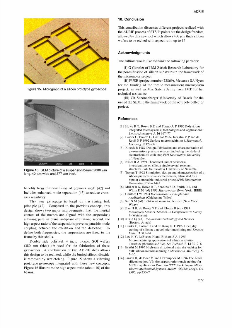
9. Silicon micromachined angular rate sensor
Low cost gyroscopes (angular rate sensors) are promising
devices for automotive applications [40–43]. In this paper,
a new silicon angular rate sensor is presented. Its design
276
8/3/2019 Advanced deep reactive ion etching: a versatile tool for microelectromechanical systems
http://slidepdf.com/reader/full/advanced-deep-reactive-ion-etching-a-versatile-tool-for-microelectromechanical 6/7
ADRIE
Figure 15. Micrograph of a silicon prototype gyroscope.
Figure 16. SEM picture of a suspension beam: 2000 µmlong, 40 µm wide and 377 µm thick.
benefits from the conclusion of previous work [42] and
includes enhanced mode separation [43] to reduce cross-
axis sensitivity.
This new gyroscope is based on the tuning fork
principle [42]. Compared to the previous concept, this
design shows two major improvements: first, the inertial
centers of the masses are aligned with the suspensions
allowing pure in plane antiphase excitation; second, the
high aspect ratio of the suspensions prevents parasitic mode
coupling between the excitation and the detection. Todefine both frequencies, the suspensions are fixed to the
frame by thin shells.
Double side polished, 4 inch, n-type, SOI wafers
(380 µm thick) are used for the fabrication of these
gyroscopes. A combination of two ADRIE steps allows
this design to be realized, while the buried silicon dioxide
is removed by wet etching. Figure 15 shows a vibrating
prototype gyroscope integrated with these new concepts.
Figure 16 illustrates the high aspect ratio (about 10) of the
beams.
10. Conclusion
This contribution discusses different projects realized with
the ADRIE process of STS. It points out the design freedom
allowed by this new tool which allows 400 µm thick silicon
wafers to be etched with aspect ratio up to 15.
Acknowledgments
The authors would like to thank the following partners:
(i) G Genolet of IBM Zurich Research Laboratory for
the porosification of silicon substrates in the framework of
the micromotor project.
(ii) FUSE (project number 22869), Mecanex SA Nyon
for the funding of the torque measurement microsystem
project, as well as Mrs Sabina Jenny from IMT for her
technical assistance.
(iii) Ch Schonenberger (University of Basel) for the
use of the SEM in the framework of the octupole deflector
project.
References
[1] Howe R T, Boser B E and Pisano A P 1996 Polysiliconintegrated microsystems: technologies and applicationsSensors Actuators A 56 167–77
[2] Linder C, Paratte L, Gretillat M-A, Jaecklin V P and deRooij N F 1992 Surface micromachining J. Micromech. Microeng. 2 122–32
[3] Kloeck B 1989 Design, fabrication and characterisation of piezoresistive pressure sensors, including the study of electrochemical etch stop PhD Dissertation Universityof Neuchatel
[4] Buser R A 1989 Theoretical and experimentalinvestigations on silicon single crystal resonantstructures PhD Dissertation University of Neuchatel
[5] Tschan T 1992 Simulation, design and characterization of asilicon piezoresistive accelerometer, fabricated by abipolar-compatible industrial process PhD DissertationUniversity of Neuchatel
[6] Muller R S, Howe R T, Senturia S D, Smith R L andWhite R M (ed) 1991 Microsensors (New York: IEEE)
[7] Gardner J W 1994 Microsensors: Principles and Applications (Chichester: Wiley)
[8] Sze S M (ed) 1994 Semiconductor Sensors (New York:Wiley)
[9] Bau H H, de Rooij N F and Kloeck B (ed) 1994 Mechanical Sensors (Sensors—a Comprehensive Survey7 (Weinheim)
[10] Ristic Lj (ed) 1994 Sensors Technology and Devices(Boston: Artech)
[11] Linder C, Tschan T and de Rooij N F 1992 Deep dry
etching of silicon: a novel micromachining tool Sensors Mater. 3 311–24
[12] Lee K Y, LaBianca H and Rishton S A 1995Micromachining applications of a high resolutionultrathick photoresist J. Vac. Sci. Technol. B 13 3012–6
[13] Esashi M 1995 High-rate directional deep dry etching forbulk silicon micromachining J. Micromech. Microeng. 55–10
[14] Jansen H, de Boer M and Elwenspoek M 1996 The black silicon method VI: high aspect ratio trench etching forMEMS applications Proc. 9th IEEE Workshop on Micro Electro Mechanical Systems, MEMS ’96 (San Diego, CA,1996) pp 250–7
277
8/3/2019 Advanced deep reactive ion etching: a versatile tool for microelectromechanical systems
http://slidepdf.com/reader/full/advanced-deep-reactive-ion-etching-a-versatile-tool-for-microelectromechanical 7/7
P-A Clerc et al
[15] Bhardwaj J K and Ashraf H 1995 Advanced silicon etchingusing high density plasmas Proc. SPIE 1995 Conf.: Micromachining and Microfabrication ProcessTechnology (Austin, TX, 1995) pp 224–33
[16] Bartha J W, Greschner J, Puech M and Maquin P 1995Low temperature etching of Si in high density plasmausing SF6 /O2 J. Microelectron. Eng. 27 453–6
[17] Coward S and Matthews D 1997 ZASE advances MEMStechnology MST News 20 23
[18] Klaasen E H, Petersen K, Noworolski J M, Logan J, Maluf N I, Brown J, Storment C, McCulley W and Kovacs GT A 1996 Silicon fusion bonding and deep reactive ionetching: a new technology for microstructures Sensors Actuators A 52 132–9
[19] Olsson A, Enoksson P, Stemme G and Stemme E 1997Micromachined flat-walled valveless diffuser pumps J. Microelectromech. Syst. 6 161–6
[20] Jaecklin V P, Linder C, de Rooij N F and Moret J M 1992Micromechanical comb actuators with low drivingvoltage J. Micromech. Microeng. 2 250–5
[21] Legtenberg R, Groeneveld A W and Elwenspoek M 1996Comb-drive actuators for large displacements J. Micromech. Microeng. 6 320–9
[22] Muller A, Gottert J and Mohr J 1993 LIGA microstructureson top of micromachined silicon wafers used to fabricatea micro-optical switch J. Micromech. Microeng. 3158–60
[23] Marxer C, Thio C, Gretillat M A, Anthamatten O, BaettigR, Valk B, Vogel P and de Rooij N F 1997 Verticalmirrors fabricated by deep reactive ion etching for fiberoptic switching applications IEEE J. Micro Electro Mech. Syst. 6 277–85
[24] Racine G-A, Genolet G, Clerc P-A, Despont M, Vettiger Pand de Rooij N F 1997 Porous silicon sacrificial layertechnique for the fabrication of free standing membraneresonators and cantilever arrays Proc. Eurosensors XI (Warsaw, 1997) vol 1, pp 285–8
[25] Beli T E, Gennissen P T J, DeMunter D and Kuhl M 1996Porous silicon as a sacrificial material J. Micromech. Microeng. 6 361–9
[26] Kaltas G and Nassiopoulos A G 1997 Application of porous silicon to bulk silicon micromachining Proc. Materials Research Society Symp. vol 459 (Pittsburgh,
PA: Materials Research Society) p 249[27] Smith R L and Collins S D 1992 Porous silicon formation
mechanisms J. Appl. Phys. 71 R1–22[28] Minne S C, Manalis S R and Quate C F 1995 Parallel
atomic force microscopy using cantilevers withintegrated piezoresistive sensors and integratedpiezoelectric actuators Appl. Phys. Lett. 67 3918
[29] Itoh T, Lee C and Suga T 1996 Deflection detection andfeedback actuation using a self-excited piezoelectricPb(Zr,Ti)O3 microcantilever for dynamic scanning forcemicroscopy Appl. Phys. Lett. 69 2036
[30] Thiebaud P, de Rooij N F, Koudelka-Hep M and StoppiniL 1997 Microelectrode arrays for electrophysiologicalmonitoring of hippocampal organotypic slice cultures IEEE Trans. Biomed. Eng. 40 1159–63
[31] Indermuhle P-F, Roth S, Dellmann L and de Rooij N FPatterned thick photoresist layers for protection of protruding structures during wet and dry etchingprocesses J. Micromech. Microeng. at press
[32] Chang T H P, Kern D P and Muray L P 1990Microminiaturization of electron optical systems J. Vac.Sci. Technol. B 8 1698
[33] Stebler C, Despont M, Staufer U, Chang T H P, Lee K Yand Rishton S A 1996 Microcolumn based low energye-beam writing Microelectron. Eng. 30 45
[34] Despont M, Staufer U, Stebler C, Gross H and Vettiger P1996 Electron-beam microcolumn fabrication and testing Microelectron. Eng. 30 69
[35] Luginbuhl Ph, Collins S D, Racine G-A, Gretillat M-A, deRooij N F, Brooks K G and Setter N 1998 Ultrasonicflexural Lamb-wave actuators based on PZT thin filmSensors Actuators A 64 41–9
[36] Gass V, van der Schoot B H, Jeanneret S and de Rooij N F1994 Micro-torque sensor based on differential forcemeasurement Proc. IEEE Micro Electro MechanicalSystems Workshop, MEMS ’94 (Oiso, 1994) pp 241–4
[37] Kanda Y 1982 A graphical representation of thepiezoresistance coefficients in silicon IEEE Trans.
Electron Devices ED-29 64–70[38] Peeters E 1994 Process development for 3D silicon
microstructures, with application to mechanical sensordevice PhD Dissertation University of Leuven
[39] Gretillat M-A, Paoletti F, Thiebaud P, Roth S,Koudelka-Hep M and de Rooij N F 1997 A new fabric-ation method for borosilicate glass capillary tubes withlateral inlets and outlets Sensors Actuators A 60 219–22
[40] Clark W-A, Howe R T and Horowitz R 1996 Siliconmicromachined Z-axis vibratory rate gyroscope Proc. IEEE Solid State Sensor and Actuator Workshop’96 (Hilton Head, SC, 1996) pp 283–7
[41] Brosnihan T-J, Bustillo J M, Pisano A P and Howe R T1997 Embedded interconnect and electrical isolation forhigh-aspect-ratio, SOI inertial instruments Dig. Tech.Papers Int. Conf. on Solid-State Sensors and Actuators,
Transducers’97 (Chicago, IL, 1997) vol 1, pp 637–40[42] Paoletti F, Gretillat M-A and de Rooij N F 1996 A silicon
micromachined vibrating gyroscope with piezoresistivedetection and electromagnetic excitation Proc. IEEE Micro Electro Mechanical Systems Workshop, MEMS ’96 (San Diego, CA, 1996) pp 162–7
[43] Wakatsuki N, Kudo S, Tanaka H, Masaaki O, Yamada S,Kikuchi K and Yamauchi M 1996 Improvement of piezoelectric vibratory gyroscope using LiTaO3 crystalProc. Symp. on Gyro Technology (Stuttgart, 1996)pp 6.0–11
278