Advanced core/multishell germanium/silicon nanowire...
3
Advanced core/multishell germanium/silicon nanowire heterostructures: Morphology and transport S. A. Dayeh, 1,a A. V. Gin, 2 and S. T. Picraux 1 1 Center for Integrated Nanotechnologies, Los Alamos National Laboratory, MS K771, Los Alamos, New Mexico 87544, USA 2 Center for Integrated Nanotechnologies, Sandia National Laboratories, MS 1303, Albuquerque, New Mexico 87185, USA Received 29 January 2011; accepted 14 March 2011; published online 22 April 2011 A precise level of control over morphology and transport in germanium/silicon core/multishell semiconductor nanowires is attained by interface engineering. Epitaxial in situ growth of such advanced heterostructures is achieved, enabling smooth and crystalline shell quality without ex situ thermal or chemical treatment. Transport simulation predicts such heterostructures with engineered energy band-edges will exhibit enhanced on-currents and transconductances over traditional device designs. Based on this synthesis approach, a 2 improvement in experimental hole mobility, transconductance, and on-currents is demonstrated for heterostructures with smooth surface morphologies compared to those with rough surface morphologies and record normalized on-currents for p-type field effect transistors are achieved. © 2011 American Institute of Physics. doi:10.1063/1.3574537 The formation of high quality epitaxial core/shell mate- rials composed of a semiconducting nanowire NW sur- rounded by one or more single crystal shells offers the op- portunity for additional control of charge transport in nanostructures. 1–6 While many NW core/shell materials sys- tems have recently gained interest, 7–11 NWs based on the germanium/silicon Ge/Si system with its 4.1% lattice mismatch are among the most interesting from technological and basic band gap engineering perspectives. 1,5,12,13 To avoid issues of Au diffusion which often accompany the synthesis of Ge/Si core/shell NWs, we utilize a growth procedure we have recently introduced that exploits a low temperature axial Si blocking layer to inhibit Au diffusion. 14 Here, we demonstrate in situ fabrication of single crystalline Ge/Si multishell radial heterostructured field effect transis- tors HFETs with and without Au diffusion and show how this approach allows NW heterostructure designs with sig- nificantly improved transconductances and hole mobilities. Our core/multishell design with engineered composition and doping demonstrate the highest reported maximum on- currents for p-type devices, an aspect of great importance for increased transistor switching speeds. Figures 1a–1d show transmission electron micro- scope images near the center of Ge NWs grown from 10, 30, 50, and 100 nm diameter Au colloids followed by a 2 min Ge shell deposition at a temperature of 410 ° C without a Si interfacial barrier layer. Rough NW surface morphology was observed indicative of locally Au-enhanced shell deposition due to Au diffusion on the NW sidewalls. With the addition of the low temperature Si interfacial barrier layer the result- ant Ge shell surface is extremely smooth for diameters 30 nm as shown in Figs. 1e–1h. For the smallest NW diameter, Au was not found at the tips of those NWs in Figs. 1a and 1e indicating loss of Au in both cases with and without a Si blocking layer during Ge shell growth, as ex- pected for sufficiently small diameters. 14 For the same growth time and temperature, the presence of Au on the NW surface leads to an enhanced growth rate of 0.375 nm / s Figs. 1e–1h whereas growth of the Ge shell without the presence of Au on the surface proceeds at a growth rate of 0.21 nm / s Figs. 1i–1l. Thus, the effect of a mono- layer of Au on the surface is to both catalyze faster deposi- tion rates and significantly increase surface roughness. For the core/shell NW growth with a Si interfacial barrier layer, the shell sidewall growth is smooth and a slight axial elon- gation occurs in conjunction with the radial shell deposition. These results demonstrate clear evidence of the effectiveness and importance of this growth procedure in inhibiting Au diffusion on the Ge NW sidewalls for the growth of high quality Ge shell layers. In addition, dopant incorporation through such controlled shell growth allows conformal and uniform distribution of dopant atoms, unlike the longitudi- nally nonuniform dopant incorporation during nominal NW growth resulting from mixed VLS and VS dopant deposition. 15 The in situ single-growth technique demonstrated in Fig. 1 for Ge/Ge core/shell NWs can also be extended to single crystal Ge/Si core/shell NWs in a single growth run without postgrowth chemical or thermal treatment. Since high tem- peratures and/or low SiH 4 partial pressures have been found to generally induce Au diffusion on Si NWs, 16 maintaining a SiH 4 partial pressure during transition from the Ge to Si growth temperature, in addition to the low temperature Si barrier layer, was necessary to avoid Au diffusion in the growth of the Si shells. Figures 1i–1k show a sequence of TEM images of Ge/Si core/shell NWs grown from 10, 30, and 50 nm diameter Au colloids without a Si barrier layer and without maintaining SiH 4 partial pressure during tem- perature ramp up, which results in Au diffusion and rough Si shell morphology. With a low temperature Si interfacial bar- rier layer and a SiH 4 partial pressure of 125 mTorr during temperature ramp up, Au diffusion on the Ge NW sidewalls was avoided and single crystal Ge/Si core/shell NWs were grown in a single growth run as demonstrated in Figs. 1l–1n. The Si shell thickness was chosen to be 3 nm, which is within the coherent critical thickness limit for all Ge a Electronic mail: [email protected]. APPLIED PHYSICS LETTERS 98, 163112 2011 0003-6951/2011/9816/163112/3/$30.00 © 2011 American Institute of Physics 98, 163112-1 Author complimentary copy. Redistribution subject to AIP license or copyright, see http://apl.aip.org/apl/copyright.jsp
Transcript of Advanced core/multishell germanium/silicon nanowire...

Advanced core/multishell germanium/silicon nanowire heterostructures:Morphology and transport
S. A. Dayeh,1,a� A. V. Gin,2 and S. T. Picraux1
1Center for Integrated Nanotechnologies, Los Alamos National Laboratory, MS K771, Los Alamos,New Mexico 87544, USA2Center for Integrated Nanotechnologies, Sandia National Laboratories, MS 1303, Albuquerque,New Mexico 87185, USA
�Received 29 January 2011; accepted 14 March 2011; published online 22 April 2011�
A precise level of control over morphology and transport in germanium/silicon core/multishellsemiconductor nanowires is attained by interface engineering. Epitaxial in situ growth of suchadvanced heterostructures is achieved, enabling smooth and crystalline shell quality without ex situthermal or chemical treatment. Transport simulation predicts such heterostructures with engineeredenergy band-edges will exhibit enhanced on-currents and transconductances over traditional devicedesigns. Based on this synthesis approach, a 2� improvement in experimental hole mobility,transconductance, and on-currents is demonstrated for heterostructures with smooth surfacemorphologies compared to those with rough surface morphologies and record normalizedon-currents for p-type field effect transistors are achieved. © 2011 American Institute of Physics.�doi:10.1063/1.3574537�
The formation of high quality epitaxial core/shell mate-rials composed of a semiconducting nanowire �NW� sur-rounded by one or more single crystal shells offers the op-portunity for additional control of charge transport innanostructures.1–6 While many NW core/shell materials sys-tems have recently gained interest,7–11 NWs based on thegermanium/silicon �Ge/Si� system with its 4.1% latticemismatch are among the most interesting from technologicaland basic band gap engineering perspectives.1,5,12,13
To avoid issues of Au diffusion which often accompanythe synthesis of Ge/Si core/shell NWs, we utilize a growthprocedure we have recently introduced that exploits a lowtemperature axial Si blocking layer to inhibit Au diffusion.14
Here, we demonstrate in situ fabrication of single crystallineGe/Si multishell radial heterostructured field effect transis-tors �HFETs� with and without Au diffusion and show howthis approach allows NW heterostructure designs with sig-nificantly improved transconductances and hole mobilities.Our core/multishell design with engineered composition anddoping demonstrate the highest reported maximum on-currents for p-type devices, an aspect of great importance forincreased transistor switching speeds.
Figures 1�a�–1�d� show transmission electron micro-scope images near the center of Ge NWs grown from 10, 30,50, and 100 nm diameter Au colloids followed by a 2 min Geshell deposition at a temperature of 410 °C without a Siinterfacial barrier layer. Rough NW surface morphology wasobserved indicative of locally Au-enhanced shell depositiondue to Au diffusion on the NW sidewalls. With the additionof the low temperature Si interfacial barrier layer the result-ant Ge shell surface is extremely smooth for diameters�30 nm as shown in Figs. 1�e�–1�h�. For the smallest NWdiameter, Au was not found at the tips of those NWs in Figs.1�a� and 1�e� indicating loss of Au in both cases �with andwithout a Si blocking layer� during Ge shell growth, as ex-pected for sufficiently small diameters.14 For the samegrowth time and temperature, the presence of Au on the NW
surface leads to an enhanced growth rate of �0.375 nm /s�Figs. 1�e�–1�h�� whereas growth of the Ge shell without thepresence of Au on the surface proceeds at a growth rate of�0.21 nm /s �Figs. 1�i�–1�l��. Thus, the effect of a mono-layer of Au on the surface is to both catalyze faster deposi-tion rates and significantly increase surface roughness. Forthe core/shell NW growth with a Si interfacial barrier layer,the shell sidewall growth is smooth and a slight axial elon-gation occurs in conjunction with the radial shell deposition.These results demonstrate clear evidence of the effectivenessand importance of this growth procedure in inhibiting Audiffusion on the Ge NW sidewalls for the growth of highquality Ge shell layers. In addition, dopant incorporationthrough such controlled shell growth allows conformal anduniform distribution of dopant atoms, unlike the longitudi-nally nonuniform dopant incorporation during nominal NWgrowth resulting from mixed VLS and VS dopantdeposition.15
The in situ single-growth technique demonstrated in Fig.1 for Ge/Ge core/shell NWs can also be extended to singlecrystal Ge/Si core/shell NWs in a single growth run withoutpostgrowth chemical or thermal treatment. Since high tem-peratures and/or low SiH4 partial pressures have been foundto generally induce Au diffusion on Si NWs,16 maintaining aSiH4 partial pressure during transition from the Ge to Sigrowth temperature, in addition to the low temperature Sibarrier layer, was necessary to avoid Au diffusion in thegrowth of the Si shells. Figures 1�i�–1�k� show a sequence ofTEM images of Ge/Si core/shell NWs grown from 10, 30,and 50 nm diameter Au colloids without a Si barrier layerand without maintaining SiH4 partial pressure during tem-perature ramp up, which results in Au diffusion and rough Sishell morphology. With a low temperature Si interfacial bar-rier layer and a SiH4 partial pressure of 125 mTorr duringtemperature ramp up, Au diffusion on the Ge NW sidewallswas avoided and single crystal Ge/Si core/shell NWs weregrown in a single growth run as demonstrated in Figs.1�l�–1�n�. The Si shell thickness was chosen to be �3 nm,which is within the coherent critical thickness limit for all Gea�Electronic mail: [email protected].
APPLIED PHYSICS LETTERS 98, 163112 �2011�
0003-6951/2011/98�16�/163112/3/$30.00 © 2011 American Institute of Physics98, 163112-1
Author complimentary copy. Redistribution subject to AIP license or copyright, see http://apl.aip.org/apl/copyright.jsp
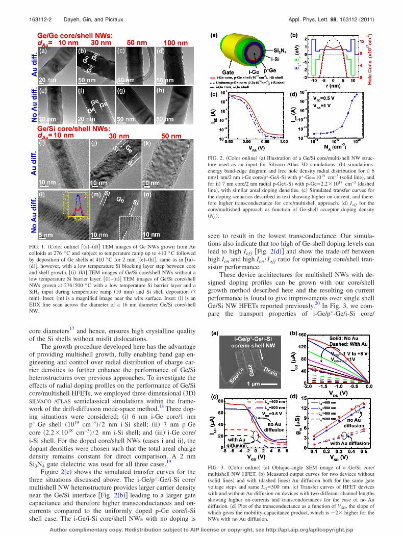
core diameters17 and hence, ensures high crystalline qualityof the Si shells without misfit dislocations.
The growth procedure developed here has the advantageof providing multishell growth, fully enabling band gap en-gineering and control over radial distribution of charge car-rier densities to further enhance the performance of Ge/Siheterostructures over previous approaches. To investigate theeffects of radial doping profiles on the performance of Ge/Sicore/multishell HFETs, we employed three-dimensional �3D�SILVACO ATLAS semiclassical simulations within the frame-work of the drift-diffusion mode-space method.18 Three dop-ing situations were considered; �i� 6 nm i-Ge core/1 nmp+-Ge shell �1019 cm−3� /2 nm i-Si shell; �ii� 7 nm p-Gecore �2.2�1018 cm−3� /2 nm i-Si shell; and �iii� i-Ge core/i-Si shell. For the doped core/shell NWs �cases i and ii�, thedopant densities were chosen such that the total areal chargedensity remains constant for direct comparison. A 2 nmSi3N4 gate dielectric was used for all three cases.19
Figure 2�c� shows the simulated transfer curves for thethree situations discussed above. The i-Ge/p+-Ge/i-Si core/multishell NW heterostructure provides larger carrier densitynear the Ge/Si interface �Fig. 2�b�� leading to a larger gatecapacitance and therefore higher transconductances and on-currents compared to the uniformly doped p-Ge core/i-Sishell case. The i-Ge/i-Si core/shell NWs with no doping is
seen to result in the lowest transconductance. Our simula-tions also indicate that too high of Ge-shell doping levels canlead to high Iof f �Fig. 2�d�� and show the trade-off betweenhigh Ion and high Ion / Iof f ratio for optimizing core/shell tran-sistor performance.
These device architectures for multishell NWs with de-signed doping profiles can be grown with our core/shellgrowth method described here and the resulting on-currentperformance is found to give improvements over single shellGe/Si NW HFETs reported previously.20 In Fig. 3, we com-pare the transport properties of i-Ge/p+-Ge/i-Si core/
FIG. 1. �Color online� ��a�–�d�� TEM images of Ge NWs grown from Aucolloids at 276 °C and subject to temperature ramp up to 410 °C followedby deposition of Ge shells at 410 °C for 2 min ��e�–�h��, same as in ��a�–�d��, however, with a low temperature Si blocking layer step between coreand shell growth. ��i�–�k�� TEM images of Ge/Si core/shell NWs without alow temperature Si barrier layer. ��l�–�n�� TEM images of Ge/Si core/shellNWs grown at 276 /500 °C with a low temperature Si barrier layer and aSiH4 input during temperature ramp �10 min� and Si shell deposition �7min�. Inset: �m� is a magnified image near the wire surface. Inset: �l� is anEDX line scan across the diameter of a 16 nm diameter Ge/Si core/shellNW.
FIG. 2. �Color online� �a� Illustration of a Ge/Si core/multishell NW struc-ture used as an input for Silvaco Atlas 3D simulations. �b� simulations:energy band-edge diagram and free hole density radial distribution for i� 6nm/1 nm/2 nm i-Ge core/p+-Ge/i-Si with p+-Ge=1019 cm−3 �solid line�, andfor ii� 7 nm core/2 nm radial p-Ge/i-Si with p-Ge=2.2�1018 cm−3 �dashedline�, with similar areal doping densities. �c� Simulated transfer curves forthe doping scenarios described in text showing higher on-current, and there-fore higher transconductance for core/multishell approach. �d� Iof f for thecore/multishell approach as function of Ge-shell acceptor doping density�NA�.
FIG. 3. �Color online� �a� Oblique-angle SEM image of a Ge/Si core/multishell NW HFET. �b� Measured output curves for two devices without�solid lines� and with �dashed lines� Au diffusion both for the same gatevoltage steps and same LG=500 nm. �c� Transfer curves of HFET deviceswith and without Au diffusion on devices with two different channel lengthsshowing higher on-currents and transconductances for the case of no Audiffusion. �d� Plot of the transconductance as a function of VSD, the slope ofwhich gives the mobility-capacitance product, which is �2� higher for theNWs with no Au diffusion.
163112-2 Dayeh, Gin, and Picraux Appl. Phys. Lett. 98, 163112 �2011�
Author complimentary copy. Redistribution subject to AIP license or copyright, see http://apl.aip.org/apl/copyright.jsp
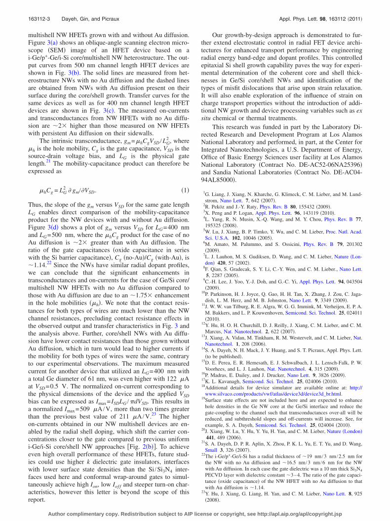
multishell NW HFETs grown with and without Au diffusion.Figure 3�a� shows an oblique-angle scanning electron micro-scope �SEM� image of an HFET device based on ai-Ge/p+-Ge/i-Si core/multishell NW heterostructure. The out-put curves from 500 nm channel length HFET devices areshown in Fig. 3�b�. The solid lines are measured from het-erostructure NWs with no Au diffusion and the dashed linesare obtained from NWs with Au diffusion present on theirsurface during the core/shell growth. Transfer curves for thesame devices as well as for 400 nm channel length HFETdevices are shown in Fig. 3�c�. The measured on-currentsand transconductances from NW HFETs with no Au diffu-sion are �2� higher than those measured on NW HFETswith persistent Au diffusion on their sidewalls.
The intrinsic transconductance, gm=�hCgVSD /LG2 , where
�h is the hole mobility, Cg is the gate capacitance, VSD is thesource-drain voltage bias, and LG is the physical gatelength.21 The mobility-capacitance product can therefore beexpressed as
�hCg = LG2 � gm/�VSD. �1�
Thus, the slope of the gm versus VSD for the same gate lengthLG enables direct comparison of the mobility-capacitanceproduct for the NW devices with and without Au diffusion.Figure 3�d� shows a plot of gm versus VSD for LG=400 nmand LG=500 nm, where the �hCg product for the case of noAu diffusion is �2� greater than with Au diffusion. Theratio of the gate capacitances �oxide capacitance in serieswith the Si barrier capacitance�, Cg �no-Au�/Cg �with-Au�, is�1.14.22 Since the NWs have similar radial dopant profiles,we can conclude that the significant enhancements intransconductances and on-currents for the case of Ge/Si core/multishell NW HFETs with no Au diffusion compared tothose with Au diffusion are due to an �1.75� enhancementin the hole mobilities ��h�. We note that the contact resis-tances for both types of wires are much lower than the NWchannel resistances, precluding contact resistance effects inthe observed output and transfer characteristics in Fig. 3 andthe analysis above. Further, core/shell NWs with Au diffu-sion have lower contact resistances than those grown withoutAu diffusion, which in turn would lead to higher currents ifthe mobility for both types of wires were the same, contraryto our experimental observations. The maximum measuredcurrent for another device that utilized an LG=400 nm witha total Ge diameter of 61 nm, was even higher with 122 �Aat VSD=0.5 V. The normalized on-current corresponding tothe physical dimensions of the device and the applied VSDbias can be expressed as Imax= ISDLG /�dVSD. This results ina normalized Imax=509 �A /V, more than two times greaterthan the previous best value of 211 �A /V.23 The higheron-currents obtained in our NW multishell devices are en-abled by the radial shell doping, which shift the carrier con-centrations closer to the gate compared to previous uniformi-Ge/i-Si core/shell NW approaches �Fig. 2�b��. To achieveeven high overall performance of these HFETs, future stud-ies could use higher k dielectric gate insulators, interfaceswith lower surface state densities than the Si /Si3N4 inter-faces used here and conformal wrap-around gates to simul-taneously achieve high Ion, low Iof f and steeper turn-on char-acteristics, however this letter is beyond the scope of thisreport.
Our growth-by-design approach is demonstrated to fur-ther extend electrostatic control in radial FET device archi-tectures for enhanced transport performance by engineeringradial energy band-edge and dopant profiles. This controlledepitaxial Si shell growth capability paves the way for experi-mental determination of the coherent core and shell thick-nesses in Ge/Si core/shell NWs and identification of thetypes of misfit dislocations that arise upon strain relaxation.It will also enable exploration of the influence of strain oncharge transport properties without the introduction of addi-tional NW growth and device processing variables such as exsitu chemical or thermal treatments.
This research was funded in part by the Laboratory Di-rected Research and Development Program at Los AlamosNational Laboratory and performed, in part, at the Center forIntegrated Nanotechnologies, a U.S. Department of Energy,Office of Basic Energy Sciences user facility at Los AlamosNational Laboratory �Contract No. DE-AC52-06NA25396�and Sandia National Laboratories �Contract No. DE-AC04-94AL85000�.
1G. Liang, J. Xiang, N. Kharche, G. Klimeck, C. M. Lieber, and M. Lund-strom, Nano Lett. 7, 642 �2007�.
2R. Peköz and J.-Y. Raty, Phys. Rev. B 80, 155432 �2009�.3X. Peng and P. Logan, Appl. Phys. Lett. 96, 143119 �2010�.4L. Yang, R. N. Musin, X.-Q. Wang, and M. Y. Chou, Phys. Rev. B 77,195325 �2008�.
5W. Lu, J. Xiang, B. P. Timko, Y. Wu, and C. M. Lieber, Proc. Natl. Acad.Sci. U.S.A. 102, 10046 �2005�.
6M. Amato, M. Palummo, and S. Ossicini, Phys. Rev. B 79, 201302�2009�.
7L. J. Lauhon, M. S. Gudiksen, D. Wang, and C. M. Lieber, Nature �Lon-don� 420, 57 �2002�.
8F. Qian, S. Gradecak, S. Y. Li, C.-Y. Wen, and C. M. Lieber., Nano Lett.5, 2287 �2005�.
9C.-H. Lee, J. Yoo, Y.-J. Doh, and G.-C. Yi, Appl. Phys. Lett. 94, 043504�2009�.
10P. Parkinson, H. J. Joyce, Q. Gao, H. H. Tan, X. Zhang, J. Zou, C. Jaga-dish, L. M. Herz, and M. B. Johnston, Nano Lett. 9, 3349 �2009�.
11J. W. W. van Tilburg, R. E. Algra, W. G. G. Immink, M. Verheijen, E. P. A.M. Bakkers, and L. P. Kouwenhoven, Semicond. Sci. Technol. 25, 024011�2010�.
12Y. Hu, H. O. H. Churchill, D. J. Reilly, J. Xiang, C. M. Lieber, and C. M.Marcus, Nat. Nanotechnol. 2, 622 �2007�.
13J. Xiang, A. Vidan, M. Tinkham, R. M. Westervelt, and C. M. Lieber, Nat.Nanotechnol. 1, 208 �2006�.
14S. A. Dayeh, N. H. Mack, J. Y. Huang, and S. T. Picraux, Appl. Phys. Lett.�to be published�.
15D. E. Perea, E. R. Hemesath, E. J. Schwalbach, J. L. Lensch-Falk, P. W.Voorhees, and L. J. Lauhon, Nat. Nanotechnol. 4, 315 �2009�.
16P. Madras, E. Dailey, and J. Drucker, Nano Lett. 9, 3826 �2009�.17K. L. Kavanagh, Semicond. Sci. Technol. 25, 024006 �2010�.18Additional details for device simulator are available online at: http://
www.silvaco.com/products/vwf/atlas/device3d/device3d_br.html.19Surface state effects are not included here and are expected to enhance
hole densities in the Ge NW core at the Ge/Si interface and reduce thegate-coupling to the channel such that transconductances over-all will bereduced, and subthreshold slopes and off-currents will increase. See, forexample, S. A. Dayeh, Semicond. Sci. Technol. 25, 024004 �2010�.
20J. Xiang, W. Lu, Y. Hu, Y. Yu, H. Yan, and C. M. Lieber, Nature �London�441, 489 �2006�.
21S. A. Dayeh, D. P. R. Aplin, X. Zhou, P. K. L. Yu, E. T. Yu, and D. Wang,Small 3, 326 �2007�.
22The i-Ge/p+-Ge/i-Si has a radial thickness of �19 nm /3 nm /2.5 nm forthe NW with no Au diffusion and �16.5 nm /3 nm /6 nm for the NWwith Au diffusion. In each case the gate dielectric was a 10 nm thick Si3N4
PECVD layer with dielectric constant �3–4. The ratio of the gate capaci-tance �oxide capacitance� of the NW HFET with no Au diffusion to thatwith Au diffusion is �1.14.
23Y. Hu, J. Xiang, G. Liang, H. Yan, and C. M. Lieber, Nano Lett. 8, 925�2008�.
163112-3 Dayeh, Gin, and Picraux Appl. Phys. Lett. 98, 163112 �2011�
Author complimentary copy. Redistribution subject to AIP license or copyright, see http://apl.aip.org/apl/copyright.jsp