ADVANCED CHIP MANUFACTURING WITH NEW MATERIALS · ›ASM technology focuses on enabling new...
34
ASM International Analyst and Investor Technology Seminar Semicon West July 13, 2016 ADVANCED CHIP MANUFACTURING WITH NEW MATERIALS
Transcript of ADVANCED CHIP MANUFACTURING WITH NEW MATERIALS · ›ASM technology focuses on enabling new...

ASM InternationalAnalyst and Investor Technology Seminar Semicon West July 13, 2016
ADVANCED CHIP MANUFACTURING WITH NEW MATERIALS

| 2
CAUTIONARY NOTE
Cautionary Note Regarding Forward-Looking Statements: All matters discussed in this
press release, except for any historical data, are forward-looking statements. Forward-
looking statements involve risks and uncertainties that could cause actual results to differ
materially from those in the forward-looking statements. These include, but are not limited
to, economic conditions and trends in the semiconductor industry generally and the timing
of the industry cycles specifically, currency fluctuations, corporate transactions, financing
and liquidity matters, the success of restructurings, the timing of significant orders, market
acceptance of new products, competitive factors, litigation involving intellectual property,
shareholders or other issues, commercial and economic disruption due to natural
disasters, terrorist activity, armed conflict or political instability, epidemics and other risks
indicated in the Company's reports and financial statements. The Company assumes no
obligation nor intends to update or revise any forward-looking statements to reflect future
developments or circumstances.

| 3
OUTLINE
› Exponentials in the industry› New Materials and 3D: Moore’s law enablers› ASM and New Materials
• ALD as enabler of new materials
• ASM New Materials development strategy
• ALD supply chain components
› ASM Products and selected applications› Summary and Conclusions
| 4
OUTLINE
› Exponentials in the industry› New Materials and 3D: Moore’s law enablers› ASM and New Materials
• ALD as enabler of new materials
• ASM New Materials development strategy
• ALD supply chain components
› ASM Products and selected applications› Summary and Conclusions

| 5
EXPONENTIALS IN THE INDUSTRY
Moore’s Law
Top: G. Moore, Electronics (1965); www.intel.com.Bottom: ASM; Techinsights and ASM (2013);
Density (xtor/chip)
Complexity (Mask Count)Memory Density (Mb/mm2)

| 6
OUTLINE
› Exponentials in the industry› New Materials and 3D: Moore’s law enablers› ASM and New Materials
• ALD as enabler of new materials
• ASM New Materials development strategy
• ALD supply chain components
› ASM Products and selected applications› Summary and Conclusions
| 7
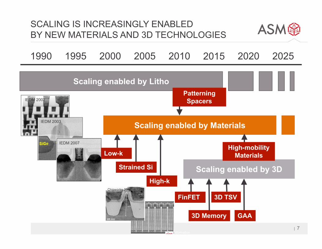
SCALING IS INCREASINGLY ENABLED BY NEW MATERIALS AND 3D TECHNOLOGIES
Scaling enabled by Litho
Scaling enabled by Materials
Scaling enabled by 3D
1995 2000 2005 2010 20151990 20252020
Strained Si
High-k
3D Memory
IEDM 2002
IEDM 2003
IEDM 2007
3D TSV
Confidential and Proprietary Information
PatterningSpacers
Low-k
FinFET
GAA
High-mobility Materials

| 8
SCALING BY MATERIALS AND 3D
2011
~2023
SiGe Si
• Density scaling (continuing Moore’s law) driving towards higher mobility materials and alternate device architectures
• Future systems will integrate much wider variety of materials and device structures

| 9
Higher Capacitance, Lower Leakage
NEW MATERIALS AND PROCESSES: MOORE’S LAW ENABLERS
High-k / Metal Gate
DRAM, RF, decoupling capacitors
Less Cross Talk, Faster Interconnect
(Porous) Low-k Materials
Improved Metals
(C) Intel
Higher Mobility, Lower Resistance
Strain and new Channel MaterialsNew metal contacts
STISi
High-k /metal gateS/D
contact
STI
Mitard et al., VLSI ‘16
Smaller Feature Sizes
SDQP for N7 and N5
E. Altamirano-Sánchez et al., SPIE Newsroom, 14 May ’16

| 10
NEW MATERIALS: MOORE’S LAW ENABLERS
10
sSOI/GeOIGe ILIII‐V IL
* GaNInSb
InGaAsGeSTORu
Other PM'sEUV
Other PM'sEUV
Co CoSi(C)P Si(C)PFDSOI FDSOISiC SiCAir AirSiCO SiCOLaO LaOLT SiO LT SiO
SiCN SiCN SiCNTiAlC MG TiAlC MG TiAlC MG
ZrO ZrO ZrOHf(Si)O Hf(Si)O Hf(Si)OAlO AlO AlOpSiOC pSiOC pSiOCSOI SOI SOI
SiGe(B) SiGe(B) SiGe(B)TaO TaO TaO TaOSOG SOG SOG SOGSiOC SiOC SiOC SiOC
Ta/TaN Ta/TaN Ta/TaN Ta/TaNCu Cu Cu CuSiOF SiOF SiOF SiOF
TiSi TiSi TiSi TiSi TiSiPtSi PtSi PtSi PtSi PtSi
TiW TiW TiW/TiN TiN TiN TiNWSi, MoSi WSi, W WSi, W W W W
BPSG BPSG BPSG BPSG BPSG BPSG BPSGAl Al Al Al Al Al Al Al
SiO, SiN SiO, SiN SiO, SiN SiO, SiN SiO, SiN SiO, SiN SiO, SiN SiO, SiNSi Si Si Si Si Si Si Si
1960 1970 1980 1990 2000 2010 2015 2020(*)
(*): Projection
Patterning RelatedBEOLFEOLStarting Materials
(IL: Interface Layer)
(PM: Patterning Materials)

| 11
OUTLINE
› Exponentials in the industry› New Materials and 3D: Moore’s law enablers› ASM and New Materials
• ALD as enabler of new materials
• ASM New Materials development strategy
• ALD supply chain components
› ASM Products and selected applications› Summary and Conclusions

| 12
ASM AND NEW MATERIALS
› ASM technology focuses on enabling new materials and new device
integration roadmapsz 3D transistor formation (FinFET & beyond FinFET)
z DRAM, Flash –planar and 3D NAND - and emerging memory
z More than Moore / IoT applications (MEMS, Sensors, Power)
› ALD (Atomic Layer Deposition) separates reactive precursors in time (or
space), and grows materials one “atomic” layer at a timez Superb control of uniformity, quality, and composition
z Conformal to any topography
› Enabling high quality materials at lower temperaturesz high-k metal gates
z low temp spacers for multi-patterning
z Other emerging applications

| 13
ALD AS ENABLER OF NEW MATERIALS -KEY STRENGTHS OF ALD
Composition Control
Excellent composition control for ternary alloys; all ALD solution demonstrated for GST
Ritala, E/Pcos 2012;
Step Coverage
42nm
43nm
AlN
Uniformity
30.5 nm AlN0.51% 3V
0.25% Full range
Interface Control
Atomically engineered interfaces to optimize leakage current, reliability and work-functions

| 14
CRITICAL ALD SUPPLY CHAIN COMPONENTS
Fundamental Capability
Process Performance Productivity Integrated
ProcessFinal Product
Capability
Pre-cursors
Pre-cursor Delivery, Valves
and Vessels
Reactors
Fab facilities,pumps & abatement
High productivity tools

| 15
OUTLINE
› Exponentials in the industry› New Materials and 3D: Moore’s law enablers› ASM and New Materials
• ALD as enabler of new materials
• ASM New Materials development strategy
• ALD supply chain components
› ASM Products and selected applications› Summary and Conclusions
| 16
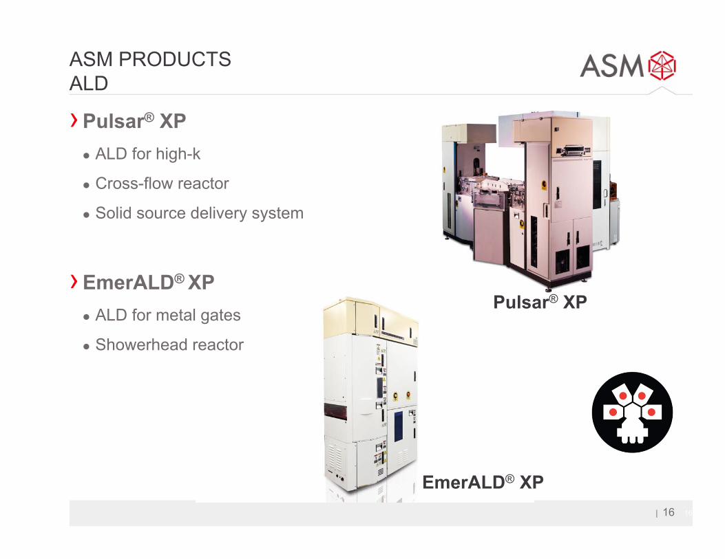
ASM PRODUCTS ALD
16
EmerALD® XP
Pulsar® XP
›Pulsar® XP z ALD for high-k
z Cross-flow reactor
z Solid source delivery system
›EmerALD® XP z ALD for metal gates
z Showerhead reactor

| 17
FINFET CHALLENGES:ALD ENABLES FURTHER SCALING IN 3D
• Materials properties and channel length must be uniform over fin height• Conformal coverage required• Aspect ratios increase going from 22nm to 14nm to 10nm• Æ ALD technology has become critical for HK and MG layers
Source: Intel

| 18
EXTENDIBILITY OF HAFNIUM BASED OXIDES
chipworks chipworks
45nm HK first RPMGPlanar FET
32 nm HK last RPMGPlanar FET
28nm HK first RPMGPlanar FET
22nm HK last RPMGFinFET
chipworks chipworks
chipworks
14nm HK last RPMGFinFET
16 nm HK last RPMGFinFET

| 19
ASM PRODUCTSPEALD AND PECVD
›XP8-DCMz High productivity single wafer tool for both PEALD and PECVD
applications
z Accommodates up to 8 chambers by DCM
z PEALD and PECVD can be integrated on the same platform
DCM (Dual Chamber Module)
| 20
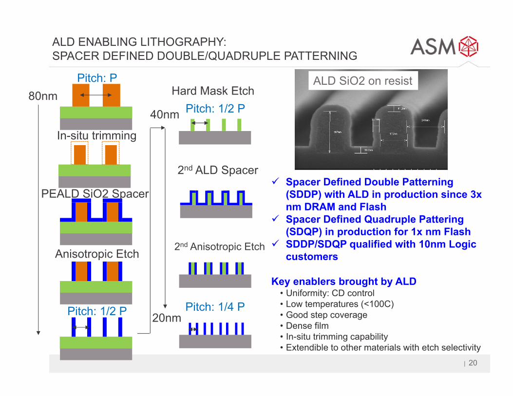
PEALD SiO2 Spacer
Anisotropic Etch
Pitch: P
Pitch: 1/2 P
80nmPitch: 1/2 P
2nd ALD Spacer
2nd Anisotropic Etch
Pitch: 1/4 P
Hard Mask Etch
20nm
ALD ENABLING LITHOGRAPHY:SPACER DEFINED DOUBLE/QUADRUPLE PATTERNING
ALD SiO2 on resist
40nm
In-situ trimming
9 Spacer Defined Double Patterning (SDDP) with ALD in production since 3x nm DRAM and Flash
9 Spacer Defined Quadruple Pattering (SDQP) in production for 1x nm Flash
9 SDDP/SDQP qualified with 10nm Logic customers
Key enablers brought by ALD• Uniformity: CD control• Low temperatures (<100C)• Good step coverage• Dense film• In-situ trimming capability• Extendible to other materials with etch selectivity

| 21
CD UNIFORMITY CONTROL
Cond ACond BCond C
� WiW uniformity is controlled by trimming and deposition� Trimming and deposition can mitigate the initial non-uniform resist pattern,
which is to help within wafer CD uniformity
Trimming SiO Deposition
Position on wafer [mm]
Position on wafer
Crit
ical
Dim
ensi
on
Position on wafer
Crit
ical
Dim
ensi
on
Position on wafer
Crit
ical
Dim
ensi
on
After lithography After trimming After SiO deposition & etch
Position on wafer [mm]
Arb
itrar
y U
nits
Arb
itrar
y U
nits

| 22
LINERS AND SPACERS FOR BEYOND 15nm FinFETs
ALD SiO2 and Si3N4 permanent spacersz Low temperature (260 ~ 550 qC)
z Conformal
z High quality (low WER, low leakage current)
40nm pitch
ALD SiO ALD SiN

| 23
Single Wafer ALD› Conformal thickness deposition is necessary for high-AR trench› The film quality of the sidewall needs to be equal to that of top/blanket› Deliver required electrical performance
Potential Applications:
Æ Development of High-temperature ALD SiO
HIGH QUALITY SIO
4. FinFET I/O Transistor Gate Oxide
IO gate SiO
Si Fin

| 24
METAL OXIDE ADVANCED HARD MASK FOR PATTERING
0
10
20
30
40
50
SiO 0.1 0.5 0.8 0.9 TiO
Dry
Etc
h R
ate
by G
as A
Dry
Etc
h R
ate
by G
as B
0
10
20
30
40
50
SiO 0.1 0.5 0.8 0.9 TiOSiO Æ SiO/Mox mix Æ Mox
ALD Mox Etching Hard Maskz Low/Tunable stress capable
z LT deposition: PR compatible
z Extension of etch selectivity portfolio
Mox
Photo Resist
SiO Æ SiO/Mox mix Æ Mox
(Arb
. Uni
ts)
(Arb
. Uni
ts)
| 25
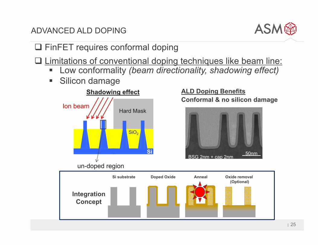
� FinFET requires conformal doping� Limitations of conventional doping techniques like beam line:� Low conformality (beam directionality, shadowing effect)� Silicon damage
Ion beam
Si
SiO2
Hard Mask
un-doped region
Shadowing effect ALD Doping Benefits Conformal & no silicon damage
ADVANCED ALD DOPING
50nmBSG 2nm + cap 2nm
Integration Concept
Doped Oxide AnnealSi substrate Oxide removal(Optional)

| 26
ASM PRODUCTS ADVANCED EPITAXY
26
Intrepid® XP
› Advanced transistors enabled with Intrepid® XPz Relaxed & strained epitaxy for Si, SiGe & Ge based
finFETs through 5nmz Channel, Source/Drain stressor, contact & passivation
cap layers
› Integrated, low thermal budget pre-clean module z High quality pre-Epi surface with low interface
contamination
› High productivity & lowest CoOz XP Platform with up to 4 process modulesz Differentiated Epi film growth enabling devices with
high drive currents & best-in-class productivityz High throughput Epi processes with excellent
uniformity, low defects & high doping levels

| 27
EPI Si:P PROCESS
› Epitaxial SiP film for nMOS finFETs
› Key Challengesz Good Epi process selectivity
z High P doping levels (>1E21 at/cm2) for lower
resistivity. • P concentration requirement increases at each node.
z Thickness and dopant uniformity and repeatability
z Low defects
z Throughput, especially at lower temps
› Integrated preclean required for pre-epi
surface control
J. Tolle, et. al., ECS 2012.

| 28
EPI LAYERS FOR POWER DEVICES
› Power devices require multiple & thick Epitaxial films to withstand high breakdown voltages (600V ~ 800V)
› Breakdown voltage of the device dictates number of Epi layers needed
› Doping level and uniformity of the Epi layers is critical and an ASM advantage
› In HVM at several power device manufacturers on 200 and 300mm
28
N+ Drain1st layer Epi
PR mask
B implant B implant
N+ Drain
1st layer Epi
2nd layer Epi3rd layer Epi
B implant B implant
PR mask
4th layer EpiMultiple epi steps

| 29
ASM PRODUCTS FURNACE CVD /DIFFUSION /BATCH ALD
› A412 PLUSz Dual boat/dual reactor systemz Clustering of different applications between reactors
possible – only vertical furnace in the market with this capability
z Up to 150 product wafer load sizez Stocker design with integrated N2-FOUP purge and
36 FOUP positions
› A400 for IoT and More than Moorez Dual boat/dual reactor system
› Applications:z Full range of applications for Logic, Memory, Power
and MEMS
z LPCVD Silicon, SiN, TEOS, HTOz Diffusion, Anneal, Cure, Reactive Curez Batch ALD (AlO, AlN, TiN, SiN, SiO, etc)
• No defects• No pattern collapse• No line wiggling

| 30
A400/A412 FURNACE - INNOVATION
Example 2: Etch stop layers (ESL)› Future nodes with complex patterning
require advanced ESL with high etch selectivity towards Si, SiO and SiN
› ESL (A** in figure below) was developed that protects substrate even for complex schemes:
Example 1: Voidless silicon gapfill. › Voidless gapfill of rectangular trenches is
a challenge for technologies beyond 10nm› Standard silicon gap fill:
› ASM solution. Voidless gap fill even for narrow widths, with high throughput:
Void
16 nm35 nm
A (ESL)
Substrate
A* (ESL)
Substrate
A** (ESL)
Substrate
Etch1 Etch2
Substrate
A* (ESL)
Substrate
A* (ESL)
SubstrateSubstrate
A** (ESL)
Substrate
A** (ESL)
Substrate
A** (ESL)
Substrate
OK
OK
OK OK
NOK; Substrate attacked
As deposited
Etch3
NOK; Substrate attacked

| 31
0
5
10
15
20
25
30
35
40
2014 2015 2016 2017 2018 2019 2020
$B
Wafer Fab Equipment by Node
7 nm and below
10 nm
14 nm
22 nm
32 nm
45 nm
65nm & above
31
WAFER FAB EQUIPMENT FORECAST
Advanced nodes: market segments with high expected growth
Gartner July, 2016
Key customer ALD penetrations in advanced nodes: market segments with high expected growth

| 32
OUTLINE
› Exponentials in the industry› New Materials and 3D: Moore’s law enablers› ASM and New Materials
• ALD as enabler of new materials
• ASM New Materials development strategy
• ALD supply chain components
› ASM Products and selected applications› Summary and Conclusions

| 33
SUMMARY AND CONCLUSIONS
› Scaling is increasingly enabled by new materials and 3D technologies
› ALD enables new materials and 3D
› Hafnium based ALD high-k gates on ASM Pulsar® extendable for 4 device generations
› ALD patterning films portfolio extended with metal oxide hardmasks
› ALD Doped oxides solution for fin doping
› High quality liners, spacers enabled by ALD
› Intrepid® XP, system with up to 4 Epi reactors, targeting strained Epi layers for CMOS, and Epsilon® 3200 for analog/power
› ASM’s Vertical Furnace is providing high productivity, in combination with continued process innovation

| 34