SHARC Processor ADSP-21367/ADSP-21368/ADSP-21369 · and the SHARC Processor .

ADSP-21065L SHARC® DSPUser’s Manual
Revision 2.0, July 2003
Part Number82-001833-01
Analog Devices, Inc.One Technology WayNorwood, Mass. 02062-9106 a

Copyright Information©2003 Analog Devices, Inc., ALL RIGHTS RESERVED. This document may not be reproduced in any form without prior, express written consent from Analog Devices, Inc.
Printed in the USA.
DisclaimerAnalog Devices, Inc. reserves the right to change this product without prior notice. Information furnished by Analog Devices is believed to be accurate and reliable. However, no responsibility is assumed by Analog Devices for its use; nor for any infringement of patents or other rights of third parties which may result from its use. No license is granted by implication or otherwise under the patent rights of Analog Devices, Inc.
Trademark and Service Mark NoticeThe Analog Devices logo, the SHARC logo, EZ-ICE, and SHARC are registered trademarks of Analog Devices, Inc.
VisualDSP++ is a trademark of Analog Devices, Inc.
All other brand and product names are trademarks or service marks of their respective owners.

ADSP-21065L SHARC DSP User’s Manual iii
CONTENTS
PREFACE
For Additional Information About Analog Products ...................... -xix
For Technical or Customer Support ............................................... -xx
What’s This Book About and Who’s It For? .................................... -xx
How to Use This Manual ............................................................ -xxii
Related Documents ..................................................................... -xxiv
Conventions of Notation .............................................................. -xxv
INTRODUCTION
Features and Benefits ..................................................................... 1-5
System-Level Enhancements .................................................... 1-6
Why Floating-Point DSP? ........................................................ 1-8
ADSP-21065L Architecture ........................................................... 1-9
DSP Core ................................................................................ 1-9
Dual-Ported Memory ............................................................ 1-16
External Port Interface ........................................................... 1-17
Host Interface ....................................................................... 1-17
I/O Processor ........................................................................ 1-18
Serial Ports ............................................................................ 1-18

CONTENTS
iv ADSP-21065L SHARC DSP User’s Manual
DMA Controller ................................................................... 1-19
Booting ................................................................................ 1-20
Development Tools ............................................................... 1-20
Summary of Features ................................................................. 1-22
Features and Benefits ............................................................ 1-22
Balanced Performance ........................................................... 1-24
Additional Literature ............................................................. 1-24
COMPUTATION UNITS
Data Formats ................................................................................ 2-4
Single-Precision Floating-Point Format .................................... 2-4
Extended-Precision FLoating-Point .......................................... 2-5
Short Word Floating-Point Format .......................................... 2-5
Exception Handling for FLoating-Point Operations ................. 2-6
Fixed-Point Format ................................................................. 2-7
Rounding Modes .................................................................... 2-7
Register File ................................................................................. 2-9
Individual Data Registers ...................................................... 2-10
Alternate Registers ................................................................ 2-11
Arithmetic Logic Unit (ALU) ...................................................... 2-12
ALU Operations ................................................................... 2-13
ALU Operating Modes .......................................................... 2-14
ALU Status Flags ................................................................... 2-16
ALU Instruction Set Summary .............................................. 2-21

ADSP-21065L SHARC DSP User’s Manual v
CONTENTS
Multiplier Unit ........................................................................... 2-26
Multiplier Operations ............................................................ 2-27
Fixed-Point Results ................................................................ 2-28
Using the MR Registers ......................................................... 2-28
Fixed-Point MR Register Operations ...................................... 2-30
Floating-Point Operating Modes ............................................ 2-32
Multiplier Status Flags ........................................................... 2-34
Multiplier Instruction Set Summary ....................................... 2-38
Shifter Unit ................................................................................ 2-41
Shifter Operations ................................................................. 2-41
Bit Field Deposit and Extract Operations ............................... 2-42
Shifter Status Flags ................................................................ 2-45
Shifter Instruction Summary .................................................. 2-47
Multifunction Operations ........................................................... 2-50
PROGRAM SEQUENCING
Instruction Cycle .......................................................................... 3-4
Program Sequencer Architecture .................................................... 3-6
Program Sequencer and System Registers ................................. 3-7
Program Sequencer Operation ..................................................... 3-10
Sequential Program Flow ....................................................... 3-10
Program Memory Data Accesses ............................................. 3-10
Branches ............................................................................... 3-11
Loops .................................................................................... 3-11

CONTENTS
vi ADSP-21065L SHARC DSP User’s Manual
Executing Conditional Instructions ............................................. 3-12
Branches (call, jump, rts, rti) ....................................................... 3-16
Delayed and Nondelayed Branches ........................................ 3-18
PC Stack ............................................................................... 3-24
Loops (DO UNTIL) ................................................................... 3-25
Restrictions and Short Loops ................................................. 3-27
Loop Address Stack ............................................................... 3-32
Loop Counters and Stack ...................................................... 3-34
Interrupts ................................................................................... 3-38
Interrupt Latency .................................................................. 3-40
Interrupt Vector Table ........................................................... 3-44
Interrupt Latch Register (IRPTL) .......................................... 3-44
Interrupt Priority .................................................................. 3-45
Interrupt Masking and Control ............................................. 3-46
Status Stack Save and Restore ................................................ 3-48
Software Interrupts ............................................................... 3-49
Clearing the Current Interrupt for Reuse ............................... 3-49
External Interrupt Timing and Sensitivity .............................. 3-50
Programmable Timers ................................................................. 3-53
Stack Flags ................................................................................. 3-54
Idle and Idle16 ........................................................................... 3-56
Instruction Cache ....................................................................... 3-58
Cache Architecture ................................................................ 3-58
Cache Efficiency ................................................................... 3-60

ADSP-21065L SHARC DSP User’s Manual vii
CONTENTS
Cache Disable and Cache Freeze ............................................ 3-61
DATA ADDRESSING
DAG Registers .............................................................................. 4-2
Alternate DAG Registers .......................................................... 4-3
DAG Operation ............................................................................ 4-6
Address Output and Modification ............................................ 4-6
Circular Buffer Addressing ....................................................... 4-9
Bit Reversal ........................................................................... 4-13
DAG Register Transfers ............................................................... 4-15
MEMORY
Transferring Data In and Out of Memory ...................................... 5-7
Dual Data Accesses .................................................................. 5-8
Using the Instruction Cache to Access PM Data ..................... 5-10
Generating Addresses for the PM and DM Buses .................... 5-11
Transferring Data Between the PM and DM Buses ................. 5-12
Memory Block Accesses and Conflicts .................................... 5-14
Memory Organization ................................................................. 5-16
Internal Memory Space .......................................................... 5-23
Multiprocessor Memory Space ............................................... 5-24
External Memory Space ......................................................... 5-26
Memory Space Access Restrictions ......................................... 5-27
Word Size and Memory Block Organization ................................ 5-28
Normal Versus Short Word Addressing ................................... 5-29
CONTENTS
viii ADSP-21065L SHARC DSP User’s Manual
Using 32- and 48-Bit Memory Words .................................... 5-30
Mixing 32- and 48-Bit Words in One Memory Block ............. 5-32
Fine Tuning Mixed Word Accesses ......................................... 5-35
Configuring Memory for 32- or 40-Bit Data .......................... 5-40
Using 16-Bit Short Word Accesses ......................................... 5-41
Interfacing with External Memory .............................................. 5-43
External Memory Banks ........................................................ 5-48
Executing Program from External Memory ............................ 5-49
Boot Memory Select (BSEL and BMS) ................................... 5-53
Wait States and Acknowledge ................................................ 5-53
External SDRAM Memory .................................................... 5-63
External Memory Access Timing ................................................. 5-65
External Memory .................................................................. 5-65
Multiprocessor Memory ........................................................ 5-67
DMA
DMA Controller Operation .......................................................... 6-7
Setting Up DMA Transfers ........................................................... 6-9
DMA Control Registers .............................................................. 6-11
External Port DMA Registers ................................................ 6-12
Serial Port DMA Control Registers ........................................ 6-22
DMA Channel Status Register ............................................... 6-24
DMA Controller Operation ........................................................ 6-27
DMA Channel Parameter Registers ........................................ 6-28
Internal Request and Grant ................................................... 6-35

ADSP-21065L SHARC DSP User’s Manual ix
CONTENTS
Setting DMA Channel Prioritization ...................................... 6-35
DMA Chaining ..................................................................... 6-39
Inserting a Chain ................................................................... 6-44
DMA Interrupts .................................................................... 6-45
Starting and Stopping DMA Sequences .................................. 6-48
External Port DMA ..................................................................... 6-50
External Port FIFO Buffers (EPBx) ........................................ 6-50
Generating Internal and External Addresses ............................ 6-55
External Port DMA Modes .................................................... 6-55
System Configurations for Interprocessor DMA ..................... 6-70
Interfacing with DMA Hardware ........................................... 6-72
Overall DMA Throughput .......................................................... 6-74
Concurrent Accesses to Internal Memory ............................... 6-74
Concurrent Accesses to External Memory ............................... 6-74
MULTIPROCESSING
Multiprocessing System Architecture ............................................. 7-6
Data Flow Multiprocessing ...................................................... 7-6
Cluster Multiprocessing ........................................................... 7-7
Multiprocessor Bus Arbitration .................................................... 7-10
Bus Arbitration Protocol ........................................................ 7-12
Bus Mastership Timeout ........................................................ 7-17
Core Priority Access ............................................................... 7-18
Bus Arbitration Synchronization After Reset .......................... 7-21
CONTENTS
x ADSP-21065L SHARC DSP User’s Manual
Data Transfers ............................................................................ 7-25
Writing the IOP Registers ..................................................... 7-26
Reading the IOP Registers ..................................................... 7-27
Transfers Through the EPBx Buffers ...................................... 7-27
Interacting with the Shadow Write FIFO ............................... 7-32
Bus Lock and Semaphores ........................................................... 7-34
Interprocessor Messages .............................................................. 7-36
Message Passing (MSGRx) .................................................... 7-37
Vector Interrupts (VIRPT) .................................................... 7-38
SYSTAT Register Status Bits ....................................................... 7-40
HOST INTERFACE
Host Control of the Processor ....................................................... 8-8
Acquiring the Bus ................................................................... 8-8
Host Transfers ....................................................................... 8-11
Asynchronous Transfer Timing .............................................. 8-11
Data Transfers ............................................................................ 8-16
Writing to the IOP Registers ................................................. 8-16
Reading the IOP Registers ..................................................... 8-17
Transfers Through the EPBx Buffers ...................................... 8-18
Performing Broadcast Writes ................................................. 8-23
Data Packing .............................................................................. 8-24
Packing Control Bits in SYSCON ......................................... 8-25
Packing Control Bits in DMACx ........................................... 8-28
Data Bus Lines and Host Bus Width ..................................... 8-30

ADSP-21065L SHARC DSP User’s Manual xi
CONTENTS
Interprocessor Messages ............................................................... 8-36
Message Passing (MSGRx) ..................................................... 8-37
Host Vector Interrupts (VIRPT) ............................................ 8-38
SYSTAT Register Bits .................................................................. 8-40
Interfacing with the System Bus .................................................. 8-44
Accessing the Cluster Bus and Slave Processors ....................... 8-44
Master Processor Accesses of the System Bus .......................... 8-46
Uniprocessor to Microprocessor Bus Interface ........................ 8-51
SERIAL PORTS
Serial Port Connections ................................................................. 9-4
SPORT Interrupts ................................................................... 9-6
SPORT RESET ............................................................................. 9-7
Using the Hardware Reset Method ........................................... 9-8
Using the Software Reset Method ............................................ 9-8
SPORT Control Registers and Data Buffers ................................... 9-9
Register Writes and Effect Latency ......................................... 9-13
Transmit and Receive Data Buffers (TX, RX) ......................... 9-13
Transmit and Receive Control Registers(STCTL, SRCTL) .............................................................. 9-15
Control Register Status Bits ................................................... 9-38
Clock and Frame Sync Frequencies(TDIV, RDIV) ................................................................... 9-39
Data Word Formats ..................................................................... 9-44
Data Type (DTYPE) .............................................................. 9-44

CONTENTS
xii ADSP-21065L SHARC DSP User’s Manual
Data Packing and Unpacking (PACK) ................................... 9-47
Endian Format (SENDN) ..................................................... 9-48
Word Length (SLEN) ............................................................ 9-48
Clock Signal Options .................................................................. 9-50
Internal vs. External Clocks ................................................... 9-50
Frame Sync Options ................................................................... 9-52
Frame Sync Requirement (TFSR/RFSR) ................................ 9-52
Frame Sync Source (ITFS/RTFS) ........................................... 9-54
Frame Sync Active State (LTFS/RTFS) ................................... 9-55
Frame Sync Clock Edge (CKRE) ........................................... 9-55
Frame Sync Insert (LAFS) ..................................................... 9-56
Frame Sync Data Dependency (DITFS) ................................. 9-57
Standard Mode ........................................................................... 9-59
Enabling Standard Mode (OPMODE, MCE) ........................ 9-59
Frame Sync Configuration (FS_BOTH) ................................ 9-59
Setting the Serial Clock Frequency (CLKDIV) ....................... 9-60
I2S Mode ................................................................................... 9-61
Setting the Internal Serial Clock Rate .................................... 9-61
I2S Control Bits .................................................................... 9-62
Multichannel Mode .................................................................... 9-67
Frame Syncs in Multichannel Mode ....................................... 9-69
Multichannel Control Bits ..................................................... 9-69
Channel Selection Registers (MTCSx, MRCSx, MTCCSx, MRCCSx) ............................ 9-72

ADSP-21065L SHARC DSP User’s Manual xiii
CONTENTS
SPORT Receive Comparison Registers (KEYWDx and IMASKx) ................................................... 9-73
Moving Data Between SPORTs and Memory ............................... 9-77
DMA Block Transfers ............................................................ 9-77
Single-Word Transfers ............................................................ 9-86
SPORT Loopback ....................................................................... 9-88
SPORT Pin Driver Considerations .............................................. 9-88
SPORT Programming Examples .................................................. 9-89
Single-Word Transfers Without Interrupts .............................. 9-89
Single-Word Transfers with Interrupts .................................... 9-91
DMA Transfers with Interrupts .............................................. 9-93
SDRAM INTERFACE
SDRAM Control Register (IOCTL) ............................................ 10-9
Configuring SDRAM Operation ............................................... 10-13
Setting the Refresh Counter Value (SDRDIV) ...................... 10-14
Setting the SDRAM Clock Enables(DSDCTL and DSDCK1) ................................................ 10-15
Setting the Number of SDRAM Banks (SDBN) ................... 10-16
Setting the External Memory Bank (SDBS) .......................... 10-16
Setting the SDRAM Buffering Option (SDBUF) .................. 10-17
Selecting the CAS Latency Value (SDCL) ............................. 10-18
Selecting the SDRAM’s Page Size (SDPGS) .......................... 10-18
Setting the SDRAM Power-Up Mode (SDPM) ..................... 10-19
Starting the SDRAM Power-Up Sequence (SDPSS) .............. 10-20

CONTENTS
xiv ADSP-21065L SHARC DSP User’s Manual
Starting Self-Refresh mode (SDSRF) ................................... 10-20
Selecting the Active Command Delay (SDTRAS) ................. 10-21
Selecting the Precharge Delay (SDTRP) ............................... 10-21
SDRAM Controller Operation .................................................. 10-23
DMA Operation ................................................................. 10-24
Multiprocessing Operation .................................................. 10-25
Accessing SDRAM .............................................................. 10-26
DQM Operation ................................................................ 10-27
Executing a Parallel Refresh Command ................................ 10-27
Entering and Exiting Self-Refresh Mode .............................. 10-28
Powering Up After Reset ..................................................... 10-28
SDRAM Controller Commands ................................................ 10-29
Act (Bank Activate) ............................................................. 10-30
Bstop (Burst Stop) .............................................................. 10-30
MRS (Mode Register Set) .................................................... 10-31
Pre (Precharge) .................................................................... 10-32
Read/Write ......................................................................... 10-33
Ref (Refresh) ....................................................................... 10-38
Sref (Self-Refresh) ............................................................... 10-39
ADSP-21065L SHARC DSP User’s Manual xv
CONTENTS
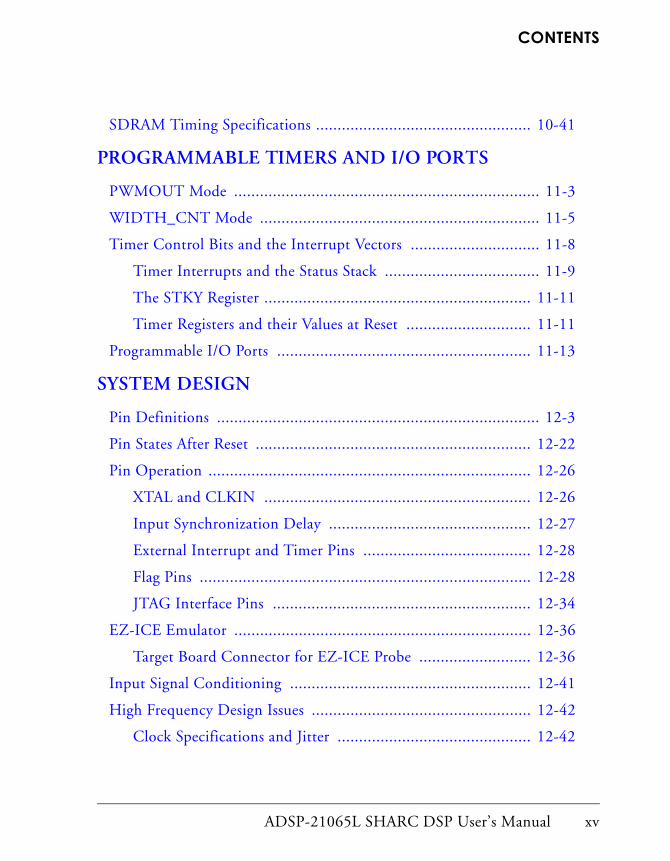
SDRAM Timing Specifications .................................................. 10-41
PROGRAMMABLE TIMERS AND I/O PORTS
PWMOUT Mode ....................................................................... 11-3
WIDTH_CNT Mode ................................................................. 11-5
Timer Control Bits and the Interrupt Vectors .............................. 11-8
Timer Interrupts and the Status Stack .................................... 11-9
The STKY Register .............................................................. 11-11
Timer Registers and their Values at Reset ............................. 11-11
Programmable I/O Ports ........................................................... 11-13
SYSTEM DESIGN
Pin Definitions ........................................................................... 12-3
Pin States After Reset ................................................................ 12-22
Pin Operation ........................................................................... 12-26
XTAL and CLKIN .............................................................. 12-26
Input Synchronization Delay ............................................... 12-27
External Interrupt and Timer Pins ....................................... 12-28
Flag Pins ............................................................................. 12-28
JTAG Interface Pins ............................................................ 12-34
EZ-ICE Emulator ..................................................................... 12-36
Target Board Connector for EZ-ICE Probe .......................... 12-36
Input Signal Conditioning ........................................................ 12-41
High Frequency Design Issues ................................................... 12-42
Clock Specifications and Jitter ............................................. 12-42

CONTENTS
xvi ADSP-21065L SHARC DSP User’s Manual
Clock Distribution .............................................................. 12-43
Point-to-Point Connections on Serial Ports .......................... 12-45
Signal Integrity ................................................................... 12-45
Other Recommendations and Suggestions ............................ 12-45
Decoupling Capacitors and Ground Planes .......................... 12-46
Oscilloscope Probes ............................................................. 12-47
Recommended Reading ....................................................... 12-47
Booting .................................................................................... 12-49
Selecting the Boot Mode ..................................................... 12-50
EPROM Booting ................................................................ 12-51
Booting From the Host ....................................................... 12-56
Multiprocessor Booting ....................................................... 12-58
No Boot Mode .................................................................... 12-60
Locating the Interrupt Vector Table ..................................... 12-61
Data Delays, Latencies, and Throughput ................................... 12-62
Execution Stalls ........................................................................ 12-66
PROGRAMMING CONSIDERATIONS
Extra Cycle Conditions ............................................................... 13-1
Nondelayed Branches ............................................................ 13-1
Program Memory Data Accesses with Cache Miss .................. 13-2
Loop Accesses of Program Memory Data ............................... 13-2
Using One- and Two-Instruction Loops ................................. 13-4
Writing to a DAG Register .................................................... 13-4
Programming Wait States ...................................................... 13-5

ADSP-21065L SHARC DSP User’s Manual xvii
Contents
Component Considerations ......................................................... 13-6
Computation Units ............................................................... 13-6
Data Address Generators ........................................................ 13-8
Memory ................................................................................ 13-9
INDEX

xviii ADSP-21065L SHARC DSP User’s Manual

ADSP-21065L SHARC DSP User’s Manual xix
PREFACEListing 1-0.
Listing 1-0.
Figure 1-0.
Table 1-0.
Congratulations on your purchase of Analog Devices ADSP-21065L
SHARC® DSP, the high-performance Digital Signal Processor of choice!
The ADSP-21065L is a 32-bit DSP with 544K bits of on-chip memory that is designed to support a wide variety of applications—audio, automo-tive, communications, industrial, and instrumentation.
For Additional Information About Analog Products
Analog Devices is online on the internet at http://www.analog.com. Our Web pages provide information on the company and products, including access to technical information and documentation, product overviews, and product announcements. You may also obtain additional information about Analog Devices and its products in any of the following ways:
• Visit our World Wide Web site at www.analog.com.
• FAX questions or requests for information to 1(617)461-3061.
• Send questions by mail to:
Analog Devices, Inc.One Technology WayP.O. Box 9106Norwood, MA 02062-9106USA

For Technical or Customer Support
xx ADSP-21065L SHARC DSP User’s Manual
• Access the division’s File Transfer Protocol (FTP) site at ftp ftp.analog.com or ftp 137.71.23.21 or ftp://ftp.anlog.com. This site is a mirror of the BBS.
For Technical or Customer SupportYou can reach our Customer Support group in the following ways:
• Visit our World Wide Web site at www.analog.com.
• Call the Analog Devices automated Customer Support Hot Line at 1(800)ANALOG-D.
• E-mail questions to [email protected] [email protected] (European customer support).
What’s This Book About and Who’s It For?The ADSP-21065L documentation set contains two manuals, the ADSP-21065L SHARC DSP User’s Manual and the ADSP-21065L SHARC DSP Technical Reference. These manuals are reference guides for hardware and software engineers who want to develop applications using the ADSP-21065L. These manuals assume the user has a working knowl-edge of the ADSP-21065L’s Super Harvard Architecture.
The ADSP-21065L SHARC DSP User’s Manual describes the architecture and operation of the ADSP-21065L’s individual components, intercom-ponent connections and access, off-chip connections and access, and the processor’s hardware/software interface. This information includes:
• Pin definitions and instructions for connecting the pins to external devices and peripherals in single- and multiprocessor systems.
• Processor features and instructions for configuring the processor for specific operation options.

ADSP-21065L SHARC DSP User’s Manual xxi
Preface
• Internal and external data paths and instructions for moving data between internal components and between the processor and exter-nal devices and peripherals.
• Timing, sequencing, and throughput of control signals and data accesses.
The ADSP-21065L SHARC DSP Technical Reference provides detailed technical information on programming the ADSP-21065L. This informa-tion includes:
• A description of each instruction in the processor’s instruction set, supported numeric formats, and the default bit definitions for all of the processor’s control and status registers.
• A description of the pins and the control and data registers of the JTAG test access port.
• A list of all vector interrupts and their addresses.
To supplement the information in these manuals, users can attend sched-uled workshops sponsored by Analog Devices, Inc. (ADI) and access other ADI documentation related specifically to this product. For details, see “Related Documents” on page xxiv.

How to Use This Manual
xxii ADSP-21065L SHARC DSP User’s Manual
How to Use This Manual
For information on… See…
ALU operation Chapter 2, Computation Units; Appendix B, Compute Operation Reference
Address generation Chapter 4, Data Addressing; Chapter 5, Mem-ory; Chapter 6, DMA
Booting Chapter 5, Memory; Chapter 7, System Design
Clock generation Chapter 9, Serial Ports; Chapter 11, Pro-grammable Timers and I/O Ports; Chapter 12, System Design
Computation units Chapter 2, Computation Units; Appendix B, Compute Operation Reference; Appendix C, Numeric Formats
Data delays,latencies,throughput
Chapter 10, SDRAM Interface; Chapter 12, System Design
Data packing Chapter 6, DMA; Chapter 8, Host Interface; Chapter 9, Serial Ports
DMA Chapter 6, DMA; Chapter 7, Multiprocessing; Chapter 8, Host Interface
External port Chapter 6, DMA; Chapter 7, Multiprocessing; Chapter 8, Host Interface
High-frequency design issues
Chapter 12, System Design
Host interface Chapter 8, Host Interface
Instruction cache Chapter 3, Program Sequencing; Chapter 5, Memory

ADSP-21065L SHARC DSP User’s Manual xxiii
Preface
Instruction set Appendix A, Instruction Set Reference; Appendix B, Compute Operation Reference; Appendix C, Numeric Formats
Internal buses Chapter 5, Memory; Chapter 6, DMA; Chapter 8, Host Interface
Interrupts Chapter 3, Program Sequencing; Chapter 5, Memory; Appendix F, Interrupt Vector Addresses
JTAG test port Chapter 12, System Design; Appendix D, JTAG Test Access Port
Memory Chapter 5, Memory
Multiplier operation Chapter2, Computation Units; Appendix B, Compute Operation Reference
Multiprocessing Chapter 7, Multiprocessing
Pin definitions Chapter 12, System Design
Processorarchitecture
Chapter 1, Introduction
Processorconfiguration
Appendix E, Control and Status Registers
Program flow Chapter 3, Program Sequencing
Programmable I/O ports
Chapter 11, Programmable Timers and I/O Ports
Programmable timers Chapter 11, Programmable Timers and I/O Ports
Programmingconsiderations
Chapter 13, Programming Considerations
For information on… See…

Related Documents
xxiv ADSP-21065L SHARC DSP User’s Manual
Related DocumentsFor information on related products, see the following documents avail-able from Analog Devices, Inc.:
• ADSP-21065L SHARC DSP, 198 MFLOPS, 3.3v Data Sheet(Rev. C, 6/03)
• VisualDSP++ Quick Installation Reference Card
• VisualDSP++ 3.0 User’s Guide for SHARC DSPs
• VisualDSP++ 3.0 Getting Started Guide for SHARC DSPs
Reset Chapter 7, Multiprocessing; Chapter 9, Serial Ports; Chapter 12, System Design
SDRAM interface Chapter 10 SDRAM Interface
Serial ports Chapter 9, Serial Ports
Shifter operation Chapter 2, Computation Units; Appendix B, Compute Operation Reference
System Design Chapter 12, System Design
Wait states Chapter 5, Memory; Chapter 12, System Design; Appendix E, Control and Status Reg-isters
Indexes Both manuals are cross-indexed. Pages with an alphabetic prefix (as C-12) reference information in ADSP-21065L SHARC DSP Techni-cal Reference. Pages with a numeric prefix (as 5-41) reference information in ADSP-21065L SHARC DSP User’s Manual.
For information on… See…
ADSP-21065L SHARC DSP User’s Manual xxv
Preface
• VisualDSP++ 3.0 C/C++ Compiler and Library Manual for SHARC DSPs
• VisualDSP++ 3.0 Linker and Utilities Manual for SHARC DSPs
• VisualDSP++ 3.0 Assembler and Preprocessor Manual for SHARC DSPs
• VisualDSP++ 3.0 Kernel (VDK) User’s Guide
• VisualDSP++ 3.0 Component Software Engineering User’s Guide
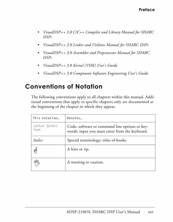
Conventions of NotationThe following conventions apply to all chapters within this manual. Addi-tional conventions that apply to specific chapters only are documented at the beginning of the chapter in which they appear.
This notation… Denotes…
Letter Gothic font
Code, software or command line options or key-words; input you must enter from the keyboard.
Italics Special terminology; titles of books.
A hint or tip.
A warning or caution.
Conventions of Notation
xxvi ADSP-21065L SHARC DSP User’s Manual

ADSP-21065L SHARC DSP User’s Manual 1-1
1 INTRODUCTIONFigure 1-0.
Table 1-0.
Listing 1-0.
The ADSP-21065L SHARC DSP is a high-performance, 32-bit digital signal processor for communications, digital audio, and industrial instru-mentation applications.
Along with a high-performance, 198 MFLOPS core, the ADSP-21065L has a dual-ported, on-chip SRAM and integrated I/O peripherals sup-ported by a dedicated I/O processor. With its on-chip instruction cache, the processor can execute every instruction in a single cycle. The ADSP-21065L is code-compatible with other members of the SHARC family.
Four independent buses for dual data, instructions, and I/O, and cross-bar-switch memory connections implement the ADSP-21065L’s Super Harvard Architecture.
The ADSP-21065L provides these features:
• 32-Bit IEEE floating-point computation units—Multiplier, ALU, and Shifter—that support 198 MFLOPS or 198, 32-bit fixed-point MOPS
• Data Register File
• Data Address Generators (DAG1, DAG2)
• Program Sequencer with Instruction Cache
• 544K bits of user-configurable, dual-ported SRAM
• External port for glueless interface to SDRAM and other off-chip memory and peripherals

1-2 ADSP-21065L SHARC DSP User’s Manual
• Host port and multiprocessor interface
• DMA controller to support ten DMA channels
• Serial ports with two receivers and two transmitters that support
TDM and I2S
• Two programmable timers and twelve programmable, general-pur-pose I/O ports
• JTAG test access port
Figure 1-1 shows the ADSP-21065L’s Super Harvard Architecture, which consists of a crossbar bus switch connecting the DSP core’s numeric pro-cessor to an independent I/O processor, dual-ported memory, and parallel system bus port.
Figure 1-1. Super Harvard Architecture
Dual-Ported,Multiaccess
Memory
NumericProcessor
I/O Processor&
DMA Controller
Parallel SystemBus Port
Crossbar BusInterconnect

ADSP-21065L SHARC DSP User’s Manual 1-3
Introduction
Figure 1-2, a detailed block diagram of the processor, shows its architec-tural features.
Figure 1-2. ADSP-21065L block diagram
Figure 1-2 also shows the ADSP-21065L’s on-chip buses: the PM (Pro-gram Memory) bus, made up of the PMA (Program Memory Address) and PMD (Program Memory Data) buses; the DM (Data Memory) bus, made up of the DMA (Data Memory Address) and DMD (Data Memory Data) buses; and the I/O bus, made up of the IOA (I/O Address) and IOD (I/O Data) buses.
The PM bus can access either instructions or data. During a single cycle, the processor can access two data operands, one over the PM bus and one over the DM bus, access an instruction from the cache, and perform a DMA transfer.
DATAADDR DATAADDR
BLO
CK
1
TWO INDEPENDENT
DUAL-PORTED BLOCKS
PROCESSORPORT
I/OPORT
ADDR DATA DATAADDR
BLO
CK
0
IOPRegisters
Control,Status, Timer,
&Data Buffers
DMAController
SPORT 0
SPORT 1
SDRAM Interface
HOST Port
Addr BusMux
Data BusMux
4
MultiprocessorInterface
DAG18x4x32
DAG28x4x24 Program
Sequencer
Instructioncache
32x48b
BusConnect
(PX)
Multiplier BarrelShifter
ALU
DataRegister
File
16x40b
24
32
48
40
PM Address Bus
DM Data Bus
PM Data Bus
DM Address Bus
7JTAGTest &
Emulation
IOA17
IOD48
24
32
(2 Rx, 2 Tx)
(2 Rx, 2 Tx)
(I2S)
(I2S)
I/O Processor
DSP Core Dual-Ported SRAM
External Port
1-4 ADSP-21065L SHARC DSP User’s Manual
The ADSP-21065L’s external port provides the processor’s interface to external memory, which is glueless to an SDRAM; memory-mapped I/O; a host processor; and another multiprocessing ADSP-21065L. The exter-nal port performs internal and external bus arbitration and supplies control signals to shared, global memory and I/O devices.
The documentation set, ADSP-21065L SHARC DSP User’s Manual and ADSP-21065L SHARC DSP Technical Reference, contain ADSP-21065L architectural information and the processor’s instruction set, which devel-opers need to design and program ADSP-21065L-based systems. For timing, electrical, and package specifications, see the processor’s data sheet.

ADSP-21065L SHARC DSP User’s Manual 1-5
Introduction
Features and BenefitsThe ADSP-21065L possesses the five central requirements for DSPs estab-lished in the ADSP-2106x SHARC DSP family of 32-bit floating-point DSPs:
• Fast, flexible arithmetic computation units
• Unconstrained data flow to and from the computation units
• Extended precision and dynamic range in the computation units
• Dual address generators
• Efficient program sequencing
Fast, Flexible Arithmetic . The ADSP-21065L executes all instructions in a single cycle. It provides fast cycle times, and, in addition to traditional multiplication, addition, subtraction, and combined multiplication/addi-tion, it also provides a complete set of arithmetic operations, including Seed 1/X, Seed 1√X, Min, Max, Clip, Shift, and Rotate. The ADSP-21065L is IEEE floating-point compatible and supports either interrupt-on-arithmetic or latched-status exception handling.
Unconstrained Data Flow. The ADSP-21065L has an enhanced Super Harvard architecture combined with a 10-port data register file. In every cycle, the processor can:
• Read or write two operands to or from the Register File,
• Supply two operands to the ALU,
• Supply two operands to the multiplier, and
• Receive two results from the ALU and multiplier.
The processor’s 48-bit orthogonal instruction word supports fully parallel data transfer and arithmetic operations in the same instruction.

Features and Benefits
1-6 ADSP-21065L SHARC DSP User’s Manual
40-Bit Extended Precision. The ADSP-21065L handles 32-bit IEEE floating-point format, 32-bit integer and fractional formats (twos-comple-ment and unsigned), and extended-precision, 40-bit IEEE floating-point format. The processor carries extended precision throughout its computa-tion units, limiting intermediate data truncation errors. When working with data on-chip, the processor can transfer the extended-precision, 32-bit mantissa to and from all computation units. The fixed-point for-mats have an 80-bit accumulator for true 32-bit fixed-point computations.
Dual Address Generators. The ADSP-21065L has two data address gener-ators (DAGs) that provide immediate or indirect (pre and postmodify) addressing. It supports modulus and bit-reverse operations with no con-straints on data buffer placement.
Efficient Program Sequencing. In addition to zero-overhead loops, the ADSP-21065L supports single-cycle setup and exit for loops. Loops are both nestable (six levels in hardware) and interruptible. The processors support both delayed and non-delayed branches.
System-Level EnhancementsThe ADSP-21065L includes several enhancements that simplify system development. The enhancements occur in three key areas:
• Architectural features supporting high-level languages and operat-ing systems
• IEEE 1149.1 JTAG serial scan path and on-chip emulation features
• Support of IEEE floating-point formats

ADSP-21065L SHARC DSP User’s Manual 1-7
Introduction
High-Level Languages. The ADSP-21065L’s architecture has several fea-tures that directly support high-level language compilers and operating systems:
• General purpose data and address register files
• 32-bit native data types
• Large address space
• Pre- and postmodify addressing
• Unconstrained circular data buffer placement
• On-chip program, loop, and interrupt stacks
Additionally, the ADSP-21065L architecture is designed specifically to support ANSI-standard Numerical C extensions—the first compiled lan-guage to support vector data types and operators for numeric and signal processing.
Serial Scan and Emulation Features. The ADSP-21065L supports the IEEE standard P1149.1 Joint Test Action Group (JTAG) standard for system test. This standard defines a method for serially scanning the I/O
status of each component in a system. The ADSP-21065L EZ-ICE® in-circuit emulator also uses the JTAG serial port to access the processor’s on-chip emulation features.
IEEE Formats. The ADSP-21065L supports IEEE floating-point data for-mats. This means that algorithms developed on IEEE-compatible processors and workstations are portable across processors without con-cern for possible instability introduced by biased rounding or inconsistent error handling.
Features and Benefits
1-8 ADSP-21065L SHARC DSP User’s Manual
Why Floating-Point DSP?A digital signal processor’s data format determines its ability to handle sig-nals of differing precision, dynamic range, and signal-to-noise ratios. However, ease-of-use and time-to-market considerations are often equally important.
Precision. The number of bits of precision of A/D converters has contin-ued to increase, and the trend is for both precision and sampling rates to increase.
Dynamic Range. Compression and decompression algorithms have tradi-tionally operated on signals of known bandwidth. These algorithms were developed to behave regularly, to keep costs down and implementations easy. Increasingly, however, the trend in algorithm development is to unconstrain the regularity and dynamic range of intermediate results. Adaptive filtering and imaging are two applications that require a wide dynamic range.
Signal-to-Noise Ratio. Audio, video, imaging, and speech recognition require wide dynamic range to discern selected signals occurring in noisy environments.
Ease-of-Use. In general, 32-bit, floating-point DSPs are easier to use and enable a quicker time-to-market than 16-bit, fixed-point processors. The extent to which this is true depends on the floating-point processor’s architecture. Consistency with IEEE workstation simulations and the elimination of scaling are two clear ease-of-use advantages. High-level lan-guage programmability, large address spaces, and wide dynamic range enable system development time to focus on algorithms and signal pro-cessing concerns, rather than assembly language coding, code paging, and error handling.
ADSP-21065L SHARC DSP User’s Manual 1-9
Introduction
ADSP-21065L ArchitectureThe rest of this chapter summarizes the architectural features of the ADSP-21065L SHARC DSP:
• DSP core
• Dual-ported memory
• External port interface
• Host processor interface
• I/O Processor
• Serial ports
• DMA controller
• Booting
• Development tools
The remaining chapters of this manual describe these features in detail.
DSP CoreThe ADSP-21065L’s DSP core consists of:
• Three computation units
• A data Register File
• A Program Sequencer and two Data Address Generators
• An Instruction Cache
• DSP core buses

ADSP-21065L Architecture
1-10 ADSP-21065L SHARC DSP User’s Manual
• Two programmable timers and 12 general-purpose I/Os
• Four external hardware interrupts
These additional features support and enhance the DSP core’s components:
• Context switching
• Comprehensive instruction set
Computation Units
The DSP core contains three independent computation units:
• ALU
Performs a standard set of arithmetic and logic operations in both fixed-point and floating-point formats.
• Multiplier with a fixed-point accumulator
Performs floating-point and fixed-point multiplication, and fixed-point multiply/add and multiply/subtract operations.
• Shifter
Performs logical and arithmetic shifts, bit manipulation, field deposit and extraction, and exponent derivation operations on 32-bit operands.
For meeting a wide variety of processing needs, the computation units process data in three formats:
• 32-bit, fixed-point
• 32-bit, floating-point
• 40-bit, floating-point
ADSP-21065L SHARC DSP User’s Manual 1-11
Introduction
The floating-point operations are single-precision, IEEE-compatible. The 32-bit floating-point format is the standard IEEE format, while the 40-bit IEEE extended-precision format has eight additional LSBs of mantissa for greater accuracy.
The computation units perform single-cycle operations—there is no com-putation pipeline. The units connect in parallel rather than serially. On the next cycle, the output of any unit can be the input of any other unit. In a multifunction computation, the ALU and multiplier perform inde-pendent, simultaneous operations.
Register File
Applications use a general-purpose data Register File to transfer data between the computation units and the data buses and to store intermedi-ate results.
For fast context switching, the Register File has two sets (primary and alternate) of 16 registers. All of the registers are 40-bits wide. The Register File, combined with the core’s Super Harvard Architecture, enables unconstrained data flow between the computation units and internal memory.
Program Sequencer and Data Address Generators
A Program Sequencer and two dedicated address generators supply addresses for memory accesses. Together the Program Sequencer and Data Address Generators (DAGs) enable computational operations to execute with maximum efficiency since they free up the computation units to pro-cess data exclusively.
Using its instruction cache, the ADSP-21065L can simultaneously fetch an instruction (from the cache) and access two data operands (from memory).

ADSP-21065L Architecture
1-12 ADSP-21065L SHARC DSP User’s Manual
The Data Address Generators implement circular data buffers in hardware.
The Program Sequencer supplies instruction addresses to program mem-ory. It controls loop iterations and evaluates conditional instructions. Using an internal loop counter and loop stack, the processor executes looped code with zero overhead. To loop or to decrement and test the counter requires no explicit jump instructions.
The processor uses pipelined fetch, decode, and execute cycles to achieve its fast execution rate. If an application uses external memories, the processor provides more time to complete an access than accesses requiring no decode cycle.
The DAGs generate memory addresses when data is transferred between memory and registers. Dual data address generators enable the processor to output simultaneous addresses for two operand reads or writes.
DAG1 supplies 32-bit addresses to data memory. DAG2 supplies 24-bit addresses to program memory for program memory data accesses.
Each DAG keeps track of up to eight address pointers, eight modifiers, and eight length values. You can modify a pointer used for indirect addressing with a value in a specified register, either before (premodify) or after (postmodify) the access. To perform automatic modulo addressing for circular data buffers, you can associate a length value with each pointer. And, you can locate circular buffers at arbitrary boundaries in memory. Each DAG register has an alternate register that you can activate for fast context switching.
Circular buffers enable efficient implementation of delay lines and other data structures required in digital signal processing and commonly used in digital filters and Fourier transforms. The DAG’s automatic handling of address pointer wraparound reduces overhead, increases performance, and simplifies implementation.
ADSP-21065L SHARC DSP User’s Manual 1-13
Introduction
Instruction Cache
The Program Sequencer includes a 32-word instruction cache that enables three-bus operation for fetching an instruction and two data values. The cache is selective—only instructions whose fetches conflict with program memory data accesses are cached. This feature enables full-speed execution of core looped operations, such as digital filter, multiply-accumulates, and FFT butterfly processing.
DSP Core Buses
The DSP core has four buses:
• Program Memory Address
Transfers the addresses for instructions.
• Data Memory Address
Transfers the addresses for data.
• Program Memory Data
Transfers instructions.
Since the PM Data bus is 48 bits wide, it can accommodate the 48-bit instruction width. Fixed-point and single-precision float-ing-point data is aligned to the upper 32 bits of this bus.
• Data Memory Data
Transfers data.
The DM Data bus is 40 bits wide and provides a path to transfer the contents of any register in the processor to any other register or to any data memory location in a single cycle. Fixed-point and sin-gle-precision floating-point data is aligned to the upper 32 bits of this bus.

ADSP-21065L Architecture
1-14 ADSP-21065L SHARC DSP User’s Manual
On the ADSP-21065L, data memory stores data operands, and program memory stores both instructions and data (filter coefficients, for example). This configuration enables the processor to perform dual data fetches when the instruction cache supplies the instruction.
The data memory address comes from one of two sources—an absolute value specified in the instruction code (direct addressing) or the output of a data address generator (indirect addressing).
Nearly every register in the ADSP-21065L’s core is classified as a universal register. Instructions are provided specifically for transferring data between universal registers or between a universal register and memory and for performing bitwise operations on their contents. Control registers, status registers, and individual data registers in the Register File are all universal registers.
The PX (bus connect) registers provide the path to pass data between the 48-bit PM Data bus and the 40-bit DM Data bus or between the 40-bit Register File and the PM Data bus. The hardware that implements these registers handles the 8-bit difference in width.
Programmable Timers and General-Purpose I/O Ports
The ADSP-21065L provides two independent programmable timer blocks. Each block can function in one of two modes—Timer Counter mode or Pulse Count and Capture mode.
In Timer Counter mode, the processor can generate a waveform with an arbitrary pulse width within a maximum period of 71.5 seconds. In Pulse Count and Capture mode, the processor can measure either the high or the low pulse width and period of an input waveform.
The ADSP-21065L provides twelve programmable, general-purpose I/O pins that can function as either input or output. As output, these pins can signal peripheral devices; as input, they can provide the test for condi-tional branching.

ADSP-21065L SHARC DSP User’s Manual 1-15
Introduction
Interrupts
The ADSP-21065L has four external hardware interrupts: three gen-eral-purpose interrupts IRQ2-0, and a special interrupt for reset. The processor also has internally generated interrupts for the timer, DMA con-troller operations, circular buffer overflow, stack overflows, arithmetic exceptions, multiprocessor vector interrupts, and user-defined software interrupts.
For the general-purpose external interrupts and the internal timer inter-rupt, the ADSP-21065L automatically stacks the arithmetic status and mode (MODE1) registers in parallel with the interrupt servicing. This enables four nesting levels of very fast service for these interrupts.
Context Switching
Many of the processor’s registers have alternate registers that applications can activate and use during interrupt servicing to implement a fast context switch.
Each of the data registers in the Register File, the DAG registers, and the multiplier result register have alternates. Registers active at reset are called primary registers, and the others are called alternate (or secondary ) regis-ters. Control bits in a mode control register determine which set of registers is active at any particular time.
Comprehensive Instruction Set
The ADSP-21065L instruction set provides a wide variety of program-ming capabilities. Multifunction instructions enable computations in parallel with data transfers and as simultaneous multiplier and ALU operations.
The addressing power of the ADSP-21065L provides flexibility in moving data both internally and externally. Every instruction can be executed in a single processor cycle. The ADSP-2106x SHARC DSP family assembly

ADSP-21065L Architecture
1-16 ADSP-21065L SHARC DSP User’s Manual
language uses an algebraic syntax for ease of coding and readability. A comprehensive set of development tools supports program development.
Dual-Ported MemoryThe ADSP-21065L contains 544K bits of on-chip SRAM, organized into two banks: Bank 0 has 288K bits, and Bank 1 has 256K bits. Bank 0 is configured with nine columns of 2Kx16 bits, and Bank 1 is configured with eight columns of 2Kx16 bits. Each memory block is dual-ported for single-cycle, independent accesses by the processor’s core and either its I/O processor or DMA controller. The dual-ported memory and separate on-chip buses allow two data transfers from the core and one from I/O, all in a single cycle.
On the ADSP-21065L, the memory can be configured as a maximum of 16K words of 32-bit data, 34K words for 16-bit data, 10K words of 48-bit instructions (and 40-bit data) or combinations of different word sizes up to 544K bits. All the memory can be accessed as 16 bit, 32 bit, or 48 bit.
The ADSP-21065L supports a 16-bit floating-point storage format, which effectively doubles the amount of data that it can store on-chip. Conver-sion between the 32-bit floating-point and 16-bit floating-point formats is done in a single instruction.
While each memory block can store combinations of code and data, accesses are most efficient when one block stores data, using the DM bus for transfers, and the other block stores instructions and data, using the PM bus for transfers. Using the DM and PM buses in this way, with one dedicated to each memory block, assures single-cycle execution with two data transfers, providing the instruction is available in the cache. Sin-gle-cycle execution is also maintained when one of the data operands is transferred to or from off-chip, through the ADSP-21065L’s external port.

ADSP-21065L SHARC DSP User’s Manual 1-17
Introduction
External Port InterfaceThe ADSP-21065L’s external port provides the processor’s interface to off-chip memory and peripherals. The 64M × 32-bit word, off-chip address space is included in the ADSP-21065L’s unified address space. The separate on-chip buses—for PM addresses, PM data, DM addresses, DM data, I/O addresses, and I/O data—are multiplexed at the external port to create an external system bus with a single 24-bit address bus and a single 32-bit data bus.
The ADSP-21065L provides an on-chip SDRAM controller that supports a glueless interface to standard 16Mb and 64Mb SDRAMs.
The on-chip decoding of high-order address lines to generate memory bank select signals facilitates the addressing of external memory devices.
The ADSP-21065L provides programmable memory wait states and exter-nal memory acknowledge controls to enable the processor to interface with peripherals with variable access, hold, and disable time requirements.
Host InterfaceThe ADSP-21065L’s host interface provides a connection to standard 8-, 16-, or 32-bit microprocessor buses that is easy and requires little addi-tional hardware.
The ADSP-21065L supports asynchronous transfers at speeds up to the processor’s full clock rate. The ADSP-21065L’s external port provides access to the processor’s host interface, which is memory mapped into the processor’s unified address space.
Two channels of DMA are available for the host interface, and they per-form code and data transfers with low software overhead. The host can directly read and write the IOP registers of the ADSP-21065L and can access the DMA channel setup and mailbox registers.

ADSP-21065L Architecture
1-18 ADSP-21065L SHARC DSP User’s Manual
Vector interrupt support provides efficient execution of host commands.
I/O ProcessorThe ADSP-21065L’s I/O Processor (IOP) includes two serial ports, each with two transmitters and two receivers, and a DMA controller.
Serial PortsThe ADSP-21065L features two synchronous serial ports that provide an inexpensive interface to a wide variety of digital and mixed-signal periph-eral devices.
The serial ports can operate at the full clock rate of the processor, provid-ing each with a maximum data rate of 30M bit/s. Each serial port has a primary and a secondary set of Tx and Rx channels, as shown in Figure 1-3.
Figure 1-3. Serial port input/output configuration
Independent transmit and receive functions provide greater flexibility for serial communications. Serial port data can be automatically transferred to and from on-chip memory through DMA. Each of the serial ports sup-
ports three operation modes: Standard mode, I2S mode (an interface

ADSP-21065L SHARC DSP User’s Manual 1-19
Introduction
commonly used by audio codecs), and TDM (Time Division Multiplex) multichannel mode.
The serial ports can operate with little-endian or big-endian transmission formats, with selectable word lengths of 3 to 32 bits. They offer selectable synchronization and transmit modes and optional µ-law or A-law com-panding. Serial port clocks and frame syncs can be internally or externally generated. The serial ports also include keyword and keymask features to enhance interprocessor communication.
DMA ControllerThe ADSP-21065L’s on-chip DMA controller enables zero-overhead data transfers without processor intervention. The DMA controller operates independently and invisibly to the processor’s core, enabling DMA opera-tions to occur while the core is simultaneously executing its program. Applications can use DMA transfers to download both code and data to the ADSP-21065L.
DMA transfers can occur between the ADSP-21065L’s internal memory and external memory, the processor’s serial ports, external peripherals, or a host processor. DMA transfers between external memory and external peripheral devices are another option. During DMA transfers, the DMA controller automatically packs and unpacks external bus words.
Ten channels of DMA are available on the ADSP-21065L—eight via the serial ports and two via the processor’s external port (for either host pro-cessor or other ADSP-21065L memory or I/O transfers).
Asynchronous off-chip peripherals can control the two external port DMA channels using the DMA request and grant lines (DMAR1-2 and DMAG1-2).
Other DMA features include interrupt generation upon completion of DMA transfers and DMA chaining for automatically linked DMA transfers.

ADSP-21065L Architecture
1-20 ADSP-21065L SHARC DSP User’s Manual
BootingApplications can boot the internal memory of the ADSP-21065L at sys-tem powerup from an 8-bit EPROM, a host processor, or external memory. The BMS (Boot Memory Select) and BSEL (EPROM Boot) pins select the boot source. Either 8-, 16-, or a 32-bit host processor can boot the ADSP-21065L.
Development ToolsThe ADSP-21065L is supported with a complete set of software and hard-ware development tools, including the EZ-ICE In-Circuit Emulator and
VisualDSP++ and SHARC tools development software.
The same EZ-ICE hardware that you use for the ADSP-21060/62, also fully emulates the ADSP-21065L, with the exception of displaying and modifying the two new SPORTs registers. The emulator will not display these two registers, but your code can still use them.
Both the SHARC DSP development tools family and the VisualDSP++ integrated project management and debugging environment support the ADSP-21065L. The VisualDSP++ project management environment enables you to develop and debug an application from within a single inte-grated program.
The SHARC DSP development tools include an easy to use assembler with instructions based on an algebraic syntax, a linker, a loader, a cycle-accurate instruction-level simulator, a C compiler, and a C run-time library that includes DSP and mathematical functions.
Debugging both C and assembly programs with the VisualDSP++ debug-ger, you can:
• View mixed C and assembly code
• Insert breakpoints
ADSP-21065L SHARC DSP User’s Manual 1-21
Introduction
• Set watchpoints
• Trace program execution
• Profile program execution
• Fill and dump memory
• Create custom debugger windows
The VisualDSP++ Integrated Development Environment (IDE) enables you to define and manage multiuser projects. Its dialog boxes and prop-erty pages enable you to configure and manage all of the SHARC DSP development tools. This capability enables you to:
• Control how the development tools process inputs and generate outputs.
• Maintain a one-to-one correspondence with the tool’scommand-line switches.
The EZ-ICE emulator uses the IEEE 1149.1 JTAG test access port of the ADSP-21065L processor to monitor and control the target board proces-sor during emulation. The EZ-ICE provides full-speed emulation to enable inspection and modification of memory, registers, and processor stacks. Use of the processor’s JTAG interface assures nonintrusive in-cir-cuit emulation—the emulator does not affect target system loading or timing.
In addition to the software and hardware development tools available from Analog Devices, third parties provide a wide range of tools support-ing the SHARC processor family.
Summary of Features
1-22 ADSP-21065L SHARC DSP User’s Manual
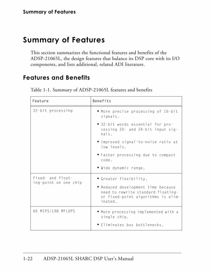
Summary of Features This section summarizes the functional features and benefits of the ADSP-21065L, the design features that balance its DSP core with its I/O components, and lists additional, related ADI literature.
Features and Benefits
Table 1-1. Summary of ADSP-21065L features and benefits
Feature Benefits
32-bit processing • More precise processing of 16-bit signals.
• 32-bit words essential for pro-cessing 20- and 24-bit input sig-nals.
• Improved signal-to-noise ratio at low levels.
• Faster processing due to compact code.
• Wide dynamic range.
Fixed- and float-ing-point on one chip
• Greater flexibility.
• Reduced development time because need to rewrite standard floating- or fixed-point algorithms is elim-inated.
66 MIPS/198 MFLOPS • More processing implemented with a single chip.
• Eliminates bus bottlenecks.
ADSP-21065L SHARC DSP User’s Manual 1-23
Introduction
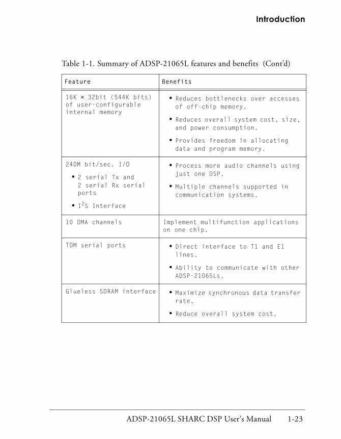
16K × 32bit (544K bits) of user-configurable internal memory
• Reduces bottlenecks over accesses of off-chip memory.
• Reduces overall system cost, size, and power consumption.
• Provides freedom in allocating data and program memory.
240M bit/sec. I/O
• 2 serial Tx and2 serial Rx serial ports
• I2S Interface
• Process more audio channels using just one DSP.
• Multiple channels supported in communication systems.
10 DMA channels Implement multifunction applications on one chip.
TDM serial ports • Direct interface to T1 and E1 lines.
• Ability to communicate with other ADSP-21065Ls.
Glueless SDRAM interface • Maximize synchronous data transfer rate.
• Reduce overall system cost.
Table 1-1. Summary of ADSP-21065L features and benefits (Cont’d)
Feature Benefits

Summary of Features
1-24 ADSP-21065L SHARC DSP User’s Manual
Balanced PerformanceFigure 1-4 shows how the ADSP-21065L’s design optimally balances its high-performance DSP core with its high-speed I/Os.
Figure 1-4. Balanced performance between the DSP core and I/O
Additional LiteratureThe following publications can be ordered from any Analog Devices sales office.
ADSP-21065L SHARC DSP, 198 MFLOPS, 3.3v Data Sheet(Rev. C, 6/03)
VisualDSP++ 3.0 User’s Guide for SHARC DSPsVisualDSP++ 3.0 Getting Started Guide for SHARC DSPsVisualDSP++ 3.0 C/C++ Compiler and Library Manual for SHARC DSPsVisualDSP++ 3.0 Linker and Utilities Manual for SHARC DSPsVisualDSP++ 3.0 Assembler and Preprocessor Manual for SHARC DSPsVisualDSP++ 3.0 Kernel (VDK) User’s GuideVisualDSP++ 3.0 Component Software Engineering User’s Guide
!"
#!$ "
!$ "
!$ "
!$ "

ADSP-21065L SHARC DSP User’s Manual 2-1
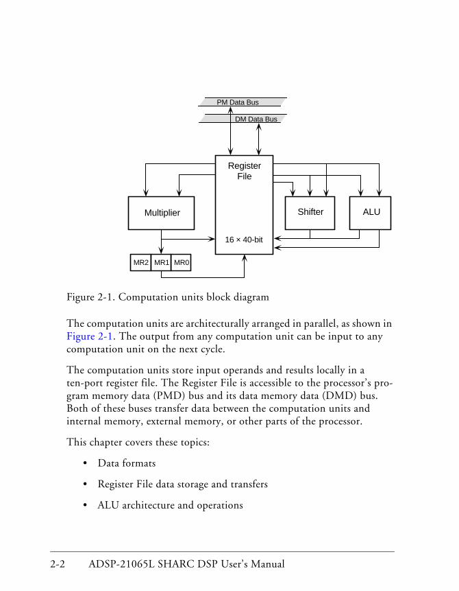
2 COMPUTATION UNITSFigure 2-0.
Table 2-0.
Listing 2-0.
The processor’s computation units provide the numeric processing power for performing DSP algorithms, performing operations on both fixed-point and floating-point numbers. Each computation unit executes instructions in a single cycle.
The processor contains three computation units:
• An arithmetic/logic unit (ALU)
Performs a standard set of arithmetic and logic operations in both fixed-point and floating-point formats.
• A multiplier
Performs floating-point and fixed-point multiplication as well as fixed-point dual multiply/add or multiply/subtract operations.
• A shifter
Performs logical and arithmetic shifts, bit manipulation, field deposit and extraction operations on 32-bit operands and can derive exponents as well.
2-2 ADSP-21065L SHARC DSP User’s Manual
Figure 2-1. Computation units block diagram
The computation units are architecturally arranged in parallel, as shown in Figure 2-1. The output from any computation unit can be input to any computation unit on the next cycle.
The computation units store input operands and results locally in a ten-port register file. The Register File is accessible to the processor’s pro-gram memory data (PMD) bus and its data memory data (DMD) bus. Both of these buses transfer data between the computation units and internal memory, external memory, or other parts of the processor.
This chapter covers these topics:
• Data formats
• Register File data storage and transfers
• ALU architecture and operations
RegisterFile
16 × 40-bit
Multiplier Shifter ALU
MR2 MR0MR1
DM Data Bus
PM Data Bus

ADSP-21065L SHARC DSP User’s Manual 2-3
Computation Units
• Multiplier architecture and operations
• Shifter architecture and operations
• Multifunction operations
Data Formats
2-4 ADSP-21065L SHARC DSP User’s Manual
Data FormatsThe processor’s computation units operate on a variety of data formats and support two rounding modes:
• IEEE 754/854 standard for single-precision floating-point format
• Extended-precision floating-point format
• Short word (16-bit) floating-point format
• 32-bit fixed-point format
• Round-toward-nearest and round-toward-zero rounding modes
The processor also provides exception handling for floating-point operations.
Single-Precision Floating-Point FormatThe processor’s Multiplier and ALU units support the single-precision, floating-point format specified in the IEEE 754/854 standard, as described in Appendix C, Numeric Formats. The processor is IEEE 754/854 compatible for single-precision, floating-point operations in all respects, except that:
• The processor does not provide inexact flags.
• NAN (Not-A-Number) inputs generate an invalid exception and return a quiet NAN (all 1s).
• The processor flushes denormal operands to 0 when they are input to a computation unit and do not generate an underflow exception.
It flushes to 0 any denormal or underflow result from an arithmetic operation and generates an underflow exception.
ADSP-21065L SHARC DSP User’s Manual 2-5
Computation Units
• The processor supports round-to-nearest and round-toward-zero modes, but does not support rounding to +Infinity or to –Infinity.
The processor also supports a 40-bit extended precision, floating-point mode, which includes eight additional LSBs of the mantissa and is compli-ant with the 754/854 standards. However, results in this format are more precise than the IEEE single-precision standard specifies.
Extended-Precision FLoating-PointFloating-point data can be either 32- or 40-bits wide. The RND32 bit in the MODE1 register determines the width:
RND32=0 Selects extended precision, floating-point format (eight bits of exponent and thirty-two bits of mantissa).
RND32=1 Selects normal IEEE precision (eight bits of exponent and twenty-four bits of mantissa).
The computation unit sets the eight LSBs of floating-point inputs to 0s before performing the operation.
It rounds the mantissa of a result to twenty-three bits (not including the hidden bit) and sets the eight LSBs of the 40-bit result to 0s to form a 32-bit number that is equivalent to the IEEE standard result.
Short Word Floating-Point FormatThe processor supports a 16-bit, floating-point data type and provides conversion instructions for it. The short float data format has an 11-bit mantissa with a 4-bit exponent and a sign bit. The 16-bit floating-point numbers reside in the lower sixteen bits of the 32-bit floating-point field.
Two shifter instructions, FPACK and FUNPACK, perform the packing and unpacking conversions between 32-bit and 16-bit floating-point
Data Formats
2-6 ADSP-21065L SHARC DSP User’s Manual
words. FPACK converts a 32-bit IEEE floating-point number to a 16-bit floating-point number. FUNPACK converts the 16-bit floating-point numbers back to 32-bit IEEE floating-point. Both instructions execute in a single cycle.
The short float type supports gradual underflow. This type sacrifices pre-cision for dynamic range. When packing a number that would have underflowed, the Shifter sets the exponent to 0 and right-shifts the man-tissa (including the hidden 1) the appropriate amount. The packed result is a denormal, which applications can unpack into a normal IEEE float-ing-point number.
Exception Handling for FLoating-Point OperationsBoth the Multiplier and ALU provide exception information when execut-ing floating-point operations. Each unit updates overflow, underflow, and invalid operation flags in the arithmetic status (ASTAT) register and in the sticky status (STKY) register. An underflow, overflow, or invalid oper-ation from any computation unit also generates a maskable interrupt. So, applications have three ways to handle floating-point exceptions:
• Interrupts
When your application must correct all exceptions as they occur, use an interrupt service routine to handle the exception condition immediately.
• ASTAT register
When your application needs to monitor a particular floating-point operation, test the exception flags in the ASTAT register that per-tain to a particular arithmetic operation after the processor has per-formed the operation.
ADSP-21065L SHARC DSP User’s Manual 2-7
Computation Units
• STKY register
When exception handling is noncritical, examine the exception flags in the STKY register at the end of a series of operations. If any flags are set, some of the results are incorrect.
Fixed-Point FormatThe processor always represents fixed-point numbers in 32-bit, left-justi-fied (occupy the thirty-two MSBs) format in its 40-bit data fields. You can treat these numbers as fractions or integers and as unsigned or twos-complement.
Each computation unit has its own restrictions on how you can mix these formats in a given operation.
The computation units read 32-bit operands from 40-bit registers, ignor-ing the eight LSBs, and write 32-bit results, zero-filling the eight LSBs.
Rounding ModesThe processor supports two modes of rounding. Both modes follow the IEEE 754 standard definitions.
• Round-Toward-Zero
If the processor cannot represent exactly the result before rounding in the destination format, it rounds the result to the number that is nearer to 0.
This method is equivalent to truncation.

Data Formats
2-8 ADSP-21065L SHARC DSP User’s Manual
• Round-Toward-Nearest
If the processor cannot represent exactly the result before rounding in the destination format, it rounds the result to the number that is nearer to the result before rounding.
If the result before rounding is exactly halfway between two num-bers in the destination format (differing by an LSB), the processor rounds the result to the number that has an LSB equal to 0.
Statistically, rounding up occurs as often as rounding down, so this method has no large sample bias.
Because the maximum floating-point value is one LSB less than the value that represents Infinity, in this mode, a result that is halfway between the maximum floating-point value and Infinity rounds to Infinity.

ADSP-21065L SHARC DSP User’s Manual 2-9
Computation Units
Register FileThe Register File provides the interface between the processor’s internal data buses and its computation units. It also provides local storage for operands and results.
The Register File has these structural and functional characteristics:
• Consists of sixteen primary registers and sixteen alternate (second-ary) registers.
• All of the individual data registers are forty bits wide.
• 32-bit data from the computation units is always left-justified.
• On register reads, the processor ignores the eight LSBs, and on reg-ister writes, it writes the eight LSBs with zeros (0).
Accesses of the Register File have these characteristics:
• Program memory data accesses and data memory accesses occur on the PM Data bus and DM Data bus, respectively.
• One PM Data bus and/or one DM Data bus access can occur in one cycle.
• Transfers between the Register File and the 40-bit DM Data bus are always forty bits wide.
• The Register File transfers data to and from the 48-bit PM Data bus in the most significant forty bits, writing zeros (0) in the lower eight bits on transfers to the PM Data bus.
Register File
2-10 ADSP-21065L SHARC DSP User’s Manual
• If the same location in the Register File is specified as both the source of an operand and the destination of a result or memory fetch, the read occurs in the first half of the cycle, and the write occurs in the second half.
This enables the processor to use the old data as the operand before it updates the location with the resulting new data.
• If writes to the same location take place in the same cycle, only the write with higher precedence actually occurs. The source of the write data determines the precedence.
In order of precedence, the sources for write data are:
• Data memory or universal register
• Program memory
• ALU
• Multiplier
• Shifter
Individual Data Registers In assembly language source code, the individual registers of the Register File carry a prefix. An F indicates floating-point computations, and an R indicates fixed-point computations.
The following instructions, for example, use the same registers:
F0=F1 * F2;floating-point multiply
R0=R1 * R2;fixed-point multiply
The F and R prefixes do not affect the 32-bit (or 40-bit) data transfer; they determine how the ALU, Multiplier, or Shifter treat the data only. You

ADSP-21065L SHARC DSP User’s Manual 2-11
Computation Units
can use either uppercase or lowercase letters for these prefixes since the assembler is case-insensitive.
Alternate RegistersTo implement fast context switching, the Register File has an a set of alternate registers. Each half of the Register File—the lower half, R0 through R7, and the upper half, R8 through R15—can independently activate its alternate register set.
Two bits in the MODE1 register select the active sets. To share data between contexts, you place the data to share in one half of the Register File and activate the alternate register set of the other half.
Note that one cycle of effect latency occurs from the time the instruction sets the bit in MODE1 to when the alternate registers are accessible.
For example,
BIT SET MODE1 SRRFL;/* activate alternate registers */NOP; /* wait until alternate registers
activate */R0=7;
Table 2-1. MODE1 bits that select the active register sets
Bit Name Definition
7 SRRFH Register file alternate select for R15-R8 (F15-F8)
10 SRRFL Register file alternate select for R7-R0 (F7-F0)

Arithmetic Logic Unit (ALU)
2-12 ADSP-21065L SHARC DSP User’s Manual
Arithmetic Logic Unit (ALU)The ALU performs arithmetic operations on fixed-point and float-ing-point data and logical operations on fixed-point data.
ALU fixed-point instructions operate on 32-bit, fixed-point operands and output 32-bit, fixed-point results.
ALU floating-point instructions operate on 32- or 40-bit, floating-point operands and output 32- or 40-bit, floating-point results.
ALU instructions include:
• Floating-point: addition, subtraction, dual addition/subtraction, average.
• Fixed-point: addition, subtraction, dual addition/subtraction, aver-age.
• Floating-point manipulation: binary log, scale, mantissa.
• Fixed-point: add with carry, subtract with borrow, increment, dec-rement.
• Logical AND, OR, XOR, NOT.
• Functions: absolute value, pass, min, max, clip, compare.
• Format conversion.
• Reciprocal and reciprocal square root primitives.
For details on dual add/subtract and parallel ALU and multiplier opera-tion, see “Multifunction Operations” on page 2-50.

ADSP-21065L SHARC DSP User’s Manual 2-13
Computation Units
ALU OperationsALU operations take one or two input operands, the X input and the Y input. These operands can be any data register in the Register File.
ALU operations usually return one result. The exceptions are:
• Dual add/subtract operations
These operations return two results.
• Compare operations
These operations return no result. They only update flags.
You can return ALU results to any location in the Register File.
The processor transfers input operands from the Register File during the first half of the cycle. It transfers results to the Register File during the sec-ond half of the cycle. This scheme enables the ALU to read and write the same location in the Register File in a single cycle.
For fixed-point operations, the processor treats both X and Y inputs as 32-bit, fixed-point operands and transfers the upper thirty-two bits from the source location in the Register File.
The results of fixed-point operations are always 32-bit, fixed-point values. Some floating-point operations (LOGB, MANT and FIX) can also yield fixed-point results. The processor transfers fixed-point results to the upper thirty-two bits of a location in the Register File and clears the lower eight bits of the location.
The format of fixed-point operands and results depends on the operation. Most arithmetic operations do not need to distinguish between integer and fraction formats. The processor treats fixed-point inputs to opera-tions, such as scaling a floating-point value, as integers. For determining status, such as overflow, the processor treats fixed-point arithmetic oper-ands and results as twos-complement numbers.

Arithmetic Logic Unit (ALU)
2-14 ADSP-21065L SHARC DSP User’s Manual
ALU Operating ModesThree bits in the MODE1 register affect the ALU:
• Saturation bit (ALUSAT)
This bit affects ALU operations that yield fixed-point results.
• Rounding mode bit (TRUNC)
• Rounding boundary bit (RND32)
Both rounding bits affect floating-point operations in both the ALU and the Multiplier.
Fixed-Point Saturation Mode
In saturation mode, all positive, fixed-point overflows cause the processor to return the maximum positive, fixed-point number (0x7FFF FFFF), and
Table 2-2. MODE1 ALU-related bits
Bit Name Description
13 ALUSAT Saturation mode.
0 = Disable ALU saturation
1 = Enable ALU saturation (full scale in fixed-point)
15 TRUNC Rounding mode.
0 = Round-to-nearest
1 = Truncation
16 RND32 Rounding boundary.
0 = Round to 40 bits
1 = Round to 32 bits

ADSP-21065L SHARC DSP User’s Manual 2-15
Computation Units
all negative overflows cause the processor to return the maximum negative number (0x8000 0000).
ALUSAT=0 Fixed-point results that overflow remain unsaturated; that is, the upper thirty-two bits of the result return unaltered.
ALUSAT=1 Fixed-point results that overflow are saturated; that is, for positive overflows, the processor returns 0x7FFF FFFF, and for negative overflows, it returns 0x8000 0000.
The ALU overflow flag reflects the ALU result before saturation.
Floating-Point Rounding Modes
The ALU supports two IEEE rounding modes. The TRUNC bit in the MODE1 register determines which rounding mode the processor uses for all ALU operations:
TRUNC=0 Selects the round-to-nearest mode.
TRUNC=1 Selects the round-to-zero mode.
Floating-Point Rounding Boundary
The results of floating-point ALU operations can be either 32-or 40-bit, floating-point data.
RND32=0 ALU inputs 40-bit operands unchanged and outputs 40-bit results from floating-point operations. Writes all 40 bits to the specified location in the Register File.
RND32=1 ALU flushes the eight LSBs of each input operand to 0s before performing the operation (except for the RND oper-ation) and outputs floating-point results in the 32-bit IEEE format. It clears the lower eight bits of the result.
In fixed-point to floating-point conversion, the rounding boundary is always forty bits, even if RND32=1.

Arithmetic Logic Unit (ALU)
2-16 ADSP-21065L SHARC DSP User’s Manual
ALU Status FlagsThe ALU updates seven status flags in the ASTAT register at the end of each operation. Table 2-3 lists and describes these ASTAT status flag bits.
The states of the seven flags reflect the result of the most recent ALU oper-ation. The ALU updates the compare accumulation (CACC) bits in ASTAT at the end of every compare operation.
The ALU also updates four sticky status flags in the STKY register, as shown in Table 2-4. Once set, a sticky flag remains high until explicitly cleared.
Table 2-3. ASTAT bit definitions for ALU status flags
Bit Name Description
0 AZ ALU result zero or floating-point underflow
1 AV ALU overflow
2 AN ALU result negative
3 AC ALU fixed-point carry
4 AS ALU X input sign (ABS, MANT operations)
5 AI ALU floating-point invalid operation
10 AF Last ALU operation was a floating-point opera-tion
24-31 CACC Compare Accumulation register (results of last eight compare operations)
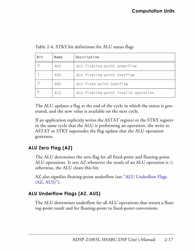
ADSP-21065L SHARC DSP User’s Manual 2-17
Computation Units
The ALU updates a flag at the end of the cycle in which the status is gen-erated, and the new value is available on the next cycle.
If an application explicitly writes the ASTAT register or the STKY register in the same cycle that the ALU is performing an operation, the write to ASTAT or STKY supersedes the flag update that the ALU operation generates.
ALU Zero Flag (AZ)
The ALU determines the zero flag for all fixed-point and floating-point ALU operations. It sets AZ whenever the result of an ALU operation is 0; otherwise, the ALU clears this bit.
AZ also signifies floating-point underflow (see "ALU Underflow Flags (AZ, AUS)").
ALU Underflow Flags (AZ, AUS)
The ALU determines underflow for all ALU operations that return a float-ing-point result and for floating-point to fixed-point conversions.
Table 2-4. STKY bit definitions for ALU status flags
Bit Name Description
0 AUS ALU floating-point underflow
1 AVS ALU floating-point overflow
2 AOS ALU fixed-point overflow
5 AIS ALU floating-point invalid operation
Arithmetic Logic Unit (ALU)
2-18 ADSP-21065L SHARC DSP User’s Manual
The ALU sets AUS whenever the result of an ALU operation is smaller than the smallest number the processor can represent in the output format.
The ALU sets AZ whenever a floating-point result is smaller than the smallest number the processor can represent in the output format.
ALU Negative Flag (AN)
The ALU determines the negative flag for all ALU operations. The ALU sets AN whenever the result of an ALU operation is negative. Otherwise, the ALU clears this bit.
ALU Overflow Flags (AV, AOS, AVS)
The ALU determines overflow for all fixed-point and floating-point ALU operations. For fixed-point results, the ALU sets AV and AOS whenever the XOR of the two most significant bits is 1. Otherwise, it clears AV.
For floating-point results, the ALU sets AV and AVS whenever the post-rounded result overflows (unbiased exponent > 127). Otherwise, it clears AV.
ALU Fixed-Point Carry Flag (AC)
The ALU determines the carry flag for all fixed-point ALU operations. For fixed-point arithmetic operations, the ALU sets AC if a carry out of the most significant bit of the result occurs. Otherwise, it clears AC.
The ALU clears AC for fixed-point logic, PASS, MIN, MAX, COMP, ABS, and CLIP operations. The ALU reads the AC flag in fixed-point addition with carry operations and in fixed-point subtraction with carry operations.

ADSP-21065L SHARC DSP User’s Manual 2-19
Computation Units
ALU Sign Flag (AS)
The ALU determines the sign flag for the fixed-point and floating-point ABS operations and the MANT operation only. The ALU sets AS if the input operand is negative. Otherwise, it clears AS.
This functionality differs from that of other ADSP-2100 family proces-sors, which do not update the AS flag on operations other than ABS.
ALU Invalid FLag (AI, AIS)
The ALU determines the invalid flag for all floating-point ALU operations.
The ALU sets AI and AIS whenever:
• An input operand is a NAN.
• The processor attempts to add oppositely signed Infinities.
• The processor attempts to subtract identically signed Infinities.
• Saturation mode is disabled, and a floating-point to fixed-point conversion results in an overflow or operates on an Infinity.
Otherwise, the ALU clears AI.
ALU Floating-Point Flag (AF)
The ALU determines AF for all fixed-point and floating-point ALU oper-ations. The ALU sets AF if the last operation was a floating-point operation. Otherwise, it clears AF.
ALU Compare Accumulation Operations
Bits 31:24 in the ASTAT register store the flag results of up to eight ALU compare operations. These bits form a right-shift register.
Arithmetic Logic Unit (ALU)
2-20 ADSP-21065L SHARC DSP User’s Manual
When the processor executes an ALU compare operation, it shifts the eight bits toward the LSB (bit 24 is lost). Then it writes the MSB, bit 31, with the result of the compare operation. If the X operand is greater than the Y operand in the compare instruction, the processor sets bit 31. Oth-erwise, it clears bit 31.
Graphics applications can use the accumulated compare flags to imple-ment two- and three-dimensional clipping operations.
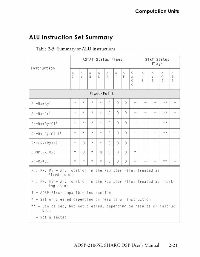
ADSP-21065L SHARC DSP User’s Manual 2-21
Computation Units
ALU Instruction Set Summary
Table 2-5. Summary of ALU instructions
Instruction
ASTAT Status Flags STKY Status Flags
AZ
AV
AN
AC
AS
AI
AF
CACC
AUS
AVS
AOS
AIS
Fixed-Point
Rn=Rx+Ry† * * * * 0 0 0 — — — ** —
Rn=Rx−RY† * * * * 0 0 0 — — — ** —
Rn=Rx+Ry+CI† * * * * 0 0 0 — — — ** —
Rn=Rx−Ry+CI−1† * * * * 0 0 0 — — — ** —
Rn=(Rx+Ry)/2 * 0 * * 0 0 0 — — — — —
COMP(Rx,Ry) * 0 * 0 0 0 0 * — — — —
Rn=Rx+CI * * * * 0 0 0 — — — ** —
Rn, Rx, Ry = Any location in the Register File; treated as fixed-point
Fn, Fx, Fy = Any location in the Register File; treated as float-ing-point
† = ADSP-21xx-compatible instruction
* = Set or cleared depending on results of instruction
** = Can be set, but not cleared, depending on results of instruc-tion
— = Not affected

Arithmetic Logic Unit (ALU)
2-22 ADSP-21065L SHARC DSP User’s Manual
Rn=Rx+CI−1 * * * * 0 0 0 — — — ** —
Rn=Rx+1 * * * * 0 0 0 — — — ** —
Rn=Rx−1 * * * * 0 0 0 — — — ** —
Rn=−Rx† * * * * 0 0 0 — — — ** —
Rn=ABS Rx† * * 0 0 * 0 0 — — — ** —
Rn=PASS Rx * 0 * 0 0 0 0 — — — — —
Rn=Rx AND Ry† * 0 * 0 0 0 0 — — — — —
Rn=Rx OR Ry† * 0 * 0 0 0 0 — — — — —
Rn=Rx XOR Ry† * 0 * 0 0 0 0 — — — — —
Table 2-5. Summary of ALU instructions (Cont’d)
Instruction
ASTAT Status Flags STKY Status Flags
AZ
AV
AN
AC
AS
AI
AF
CACC
AUS
AVS
AOS
AIS
Rn, Rx, Ry = Any location in the Register File; treated as fixed-point
Fn, Fx, Fy = Any location in the Register File; treated as float-ing-point
† = ADSP-21xx-compatible instruction
* = Set or cleared depending on results of instruction
** = Can be set, but not cleared, depending on results of instruc-tion
— = Not affected

ADSP-21065L SHARC DSP User’s Manual 2-23
Computation Units
Rn=NOT Rx† * 0 * 0 0 0 0 — — — — —
Rn=MIN(Rx, Ry) * 0 * 0 0 0 0 — — — — —
Rn=MAX(Rx, Ry) * 0 * 0 0 0 0 — — — — —
Rn=CLIP Rx BY Ry * 0 * 0 0 0 0 — — — — —
Floating-Point
Fn=Fx+Fy * * * 0 0 * 1 — ** ** — **
Fn=Fx−Fy * * * 0 0 * 1 — ** ** — **
Fn=ABS(Fx+Fy) * * 0 0 0 * 1 — ** ** — **
Fn=ABS(Fx−Fy) * * 0 0 0 * 1 — ** ** — **
Fn=(Fx+Fy)/2 * 0 * 0 0 * 1 — ** — — **
Table 2-5. Summary of ALU instructions (Cont’d)
Instruction
ASTAT Status Flags STKY Status Flags
AZ
AV
AN
AC
AS
AI
AF
CACC
AUS
AVS
AOS
AIS
Rn, Rx, Ry = Any location in the Register File; treated as fixed-point
Fn, Fx, Fy = Any location in the Register File; treated as float-ing-point
† = ADSP-21xx-compatible instruction
* = Set or cleared depending on results of instruction
** = Can be set, but not cleared, depending on results of instruc-tion
— = Not affected
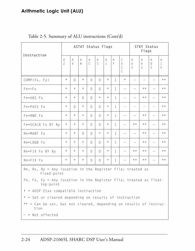
Arithmetic Logic Unit (ALU)
2-24 ADSP-21065L SHARC DSP User’s Manual
COMP(Fx, Fy) * 0 * 0 0 * 1 * — — — **
Fn=−Fx * * * 0 0 * 1 — — ** — **
Fn=ABS Fx * * 0 0 * * 1 — — ** — **
Fn=PASS Fx * 0 * 0 0 * 1 — — — — **
Fn=RND Fx * * * 0 0 * 1 — — ** — **
Fn=SCALB Fx BY Ry * * * 0 0 * 1 — ** ** — **
Rn=MANT Fx * * 0 0 * * 1 — — ** — **
Rn=LOGB Fx * * * 0 0 * 1 — — ** — **
Rn=FIX Fx BY Ry * * * 0 0 * 1 — ** ** — **
Rn=FIX Fx * * * 0 0 * 1 — ** ** — **
Table 2-5. Summary of ALU instructions (Cont’d)
Instruction
ASTAT Status Flags STKY Status Flags
AZ
AV
AN
AC
AS
AI
AF
CACC
AUS
AVS
AOS
AIS
Rn, Rx, Ry = Any location in the Register File; treated as fixed-point
Fn, Fx, Fy = Any location in the Register File; treated as float-ing-point
† = ADSP-21xx-compatible instruction
* = Set or cleared depending on results of instruction
** = Can be set, but not cleared, depending on results of instruc-tion
— = Not affected

ADSP-21065L SHARC DSP User’s Manual 2-25
Computation Units
For details on each of the ALU instructions, see “ALU Operations” on page B-2, in ADSP-21065L SHARC DSP Technical Reference.
Fn=FLOAT Rx BY Ry * * * 0 0 0 1 — ** ** — —
Fn=FLOAT Rx * 0 * 0 0 0 1 — — — — —
Fn=RECIPS Fx * * * 0 0 * 1 — ** ** — **
Fn=RSQRTS Fx * * * 0 0 * 1 — — ** — **
Fn=Fx COPYSIGN Fy * 0 * 0 0 * 1 — — — — **
Fn=MIN(Fx, Fy) * 0 * 0 0 * 1 — — — — **
Fn=MAX(Fx, Fy) * 0 * 0 0 * 1 — — — — **
Fn=CLIP Fx BY Fy * 0 * 0 0 * 1 — — — — **
Table 2-5. Summary of ALU instructions (Cont’d)
Instruction
ASTAT Status Flags STKY Status Flags
AZ
AV
AN
AC
AS
AI
AF
CACC
AUS
AVS
AOS
AIS
Rn, Rx, Ry = Any location in the Register File; treated as fixed-point
Fn, Fx, Fy = Any location in the Register File; treated as float-ing-point
† = ADSP-21xx-compatible instruction
* = Set or cleared depending on results of instruction
** = Can be set, but not cleared, depending on results of instruc-tion
— = Not affected
Multiplier Unit
2-26 ADSP-21065L SHARC DSP User’s Manual
Multiplier UnitThe Multiplier performs fixed-point or floating-point multiplication and fixed-point, multiply and accumulate operations.
It can perform fixed-point, multiply and accumulates with either cumula-tive addition or cumulative subtraction.
Through parallel operation of the ALU and Multiplier, using multifunc-tion instructions, applications can perform floating-point, multiply and accumulates. See “Multifunction Operations” on page 2-50.
Multiplier fixed-point instructions operate on 32-bit, fixed-point data and produce 80-bit results. These instructions treat inputs as fractional or integer, unsigned or twos-complement.
Multiplier floating-point instructions operate on 32- or 40-bit float-ing-point operands and output 32- or 40-bit floating-point results.
Multiplier instructions include:
• 32-bit, fixed-point multiplication.
• Fixed-point multiply and accumulate to eighty bits (with addition), with rounding optional.
• Fixed-point multiply and accumulate to eighty bits (with subtrac-tion), rounding optional.
• Round result register.
• Saturate result register.
• Clear result register.
• Floating-point multiplication.
ADSP-21065L SHARC DSP User’s Manual 2-27
Computation Units
Multiplier OperationsThe Multiplier takes two input operands, the X-input and the Y-input. These operands can be any of the data registers in the Register File.
Fixed-point operations can accumulate fixed-point results in either of the Multiplier’s two local result registers (MR) or write results back to the Register File. The processor can round or saturate results stored in the MR registers in separate operations.
Floating-point operations yield floating-point results, which the processor always writes directly back to the Register File.
The processor transfers input operands during the first half of the cycle and results during the second half of the cycle. This enables the Multiplier to read and write the same location in the Register File within a single cycle.
In fixed-point operations that use inputs from the Register File, the pro-cessor reads from the upper thirty-two bits of the source location.
You can input fixed-point operands in either integer or fractional format, but both operands must in the same format. The format of the result is the same as the format of the inputs.
You can input each fixed-point operand as either an unsigned or a twos-complement number. If both inputs are fractional and signed, the Multiplier automatically shifts the result left one bit to remove the redun-dant sign bit.
You specify the input data type within the multiplier instruction.
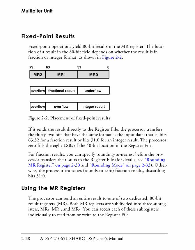
Multiplier Unit
2-28 ADSP-21065L SHARC DSP User’s Manual
Fixed-Point ResultsFixed-point operations yield 80-bit results in the MR register. The loca-tion of a result in the 80-bit field depends on whether the result is in fraction or integer format, as shown in Figure 2-2.
Figure 2-2. Placement of fixed-point results
If it sends the result directly to the Register File, the processor transfers the thirty-two bits that have the same format as the input data; that is, bits 63:32 for a fraction result or bits 31:0 for an integer result. The processor zero-fills the eight LSBs of the 40-bit location in the Register File.
For fraction results, you can specify rounding-to-nearest before the pro-cessor transfers the results to the Register File (for details, see “Rounding MR Register” on page 2-30 and “Rounding Mode” on page 2-33). Other-wise, the processor truncates (rounds-to-zero) fraction results, discarding bits 31:0.
Using the MR RegistersThe processor can send an entire result to one of two dedicated, 80-bit result registers (MR). Both MR registers are subdivided into three subreg-isters, MR2, MR1, and MR0. You can access each of these subregisters individually to read from or write to the Register File.

ADSP-21065L SHARC DSP User’s Manual 2-29
Computation Units
When reading data from MR2, the processor sign-extends the data to thirty-two bits (see Figure 2-3). When reading data from MR2, MR1, or MR0 and writing it to the Register File, the processor zero-fills the eight LSBs of the 40-bit location in the Register File.
Figure 2-3. MR transfer formats
The processor writes into MR2, MR1, or MR0 data from the thirty-two MSBs of a location in the Register File, ignoring the eight LSBs. It sign-extends into MR2 the data it wrote into MR1; that is, the processor repeats the MSB of MR1 in the sixteen bits of MR2. The processor does not sign-extend the data it writes to MR0.
The two MR registers are designated MRF (foreground) and MRB (back-ground). Foreground registers are those that the SRCU bit in the MODE1 register is currently activating, and background registers are those it is currently deactivating.
In the case where only one MR register is used at a time, the SRCU bit activates one or the other to implement context switching. However, unlike other registers for which alternate sets exist, both MR register sets are accessible at the same time.
All (fixed-point) accumulation instructions can specify either result regis-ter for accumulation, regardless of the state of the SRCU bit. So, instead of using the MR registers as primary and alternate registers, you can use
Sign Extend MR2 Zeros
16 bits 16 bits 16 bits
8-bits32-bits
MR0 Zeros
MR1 Zeros
8 bits32 bits
Multiplier Unit
2-30 ADSP-21065L SHARC DSP User’s Manual
them as two parallel accumulators. This feature supports complex math operations.
Transfers between MR registers and the Register File are considered com-putation unit operations since they involve the Multiplier. So, although the syntax for the transfer is the same as for any other transfer to or from the Register File, you specify an MR transfer in an instruction where a computation is normally specified. For example, the processor can per-form a multiply and accumulate in parallel with a data memory read, as in:
MRF=MRF-R5*R0, R6=DM(I1,M2),
or it can perform an MR transfer instead of the computation, as in:
R5=MR1F, R6=DM(I1,M2)
Fixed-Point MR Register OperationsIn addition to multiplication, fixed-point operations include accumula-tion, rounding, and saturation of fixed-point data. The three MR register operations are:
• Clear MR register
• Round MR register
• Saturate MR register
Clear MR Register
This operation resets the specified MR register to 0. Performed at the start of a multiply and accumulate operation, it removes results left over from the previous operation.
Rounding MR Register
Rounding of a fixed-point result occurs either as part of a multiply, a mul-tiply and accumulate, or an explicit operation on the MR register.

ADSP-21065L SHARC DSP User’s Manual 2-31
Computation Units
This operation applies only to fraction results (integer results are not affected) and rounds the 80-bit MR value to nearest at bit 32; that is, at the MR1-MR0 boundary.
Applications can send the rounded result in MR1 either to the Register File or back to the same MR register.
To round a fraction result to 0 (truncation) instead of to nearest, you sim-ply transfer the unrounded result from MR1, discarding the lower thirty-two bits in MR0.
Saturate MR Register
This operation sets MR to a maximum value if the MR value has over-flowed. Overflow occurs when the MR value is greater than the maximum value for the data format (unsigned or twos-complement and integer or fractional) that is specified in the saturate instruction.
This operation has six possible maximum values (values are in hexadeci-mal), as shown in Table 2-6.
Table 2-6. Valid MR maximum saturation values
Data Format MR2 MR1 MR0 Sign
Max. 2s-comp., Fractional
0000 7FFF FFFF FFFF FFFF +
FFFF 8000 0000 0000 0000 −
Max. 2s-comp., Integer
0000 0000 0000 7FFF FFFF +
FFFF FFFF FFFF 8000 0000 −
Max. unsigned, Fractional
0000 FFFF FFFF FFFF FFFF
Max. unsigned, Integer
0000 0000 0000 FFFF FFFF

Multiplier Unit
2-32 ADSP-21065L SHARC DSP User’s Manual
You can send the result from MR saturation to either the Register File or back to the same MR register.
Floating-Point Operating ModesTwo mode status bits in the MODE1 register affect multiplier (and ALU) operations:
• Rounding mode (TRUNC)
• Rounding boundary bits (RND32)
Although the processor supports these two rounding modes for fixed-point multiplier operations on fraction data, the Multiplier performs the round-to-nearest operation only. This is so because the Multiplier has a local result register for fixed-point operations, and it reads only the upper bits of the result and discards the lower bits, implicitly rounding-to-zero.
Table 2-7. MODE1 ALU and Multiplier operation status bits
Bit Name Description
0 TRUNC Rounding mode.
0= Round-to-nearest
1= Truncate
1 RND32 Rounding boundary.
0= Round to 40 bits
1= Round to 32 bits
ADSP-21065L SHARC DSP User’s Manual 2-33
Computation Units
Rounding Mode
The Multiplier supports two IEEE rounding modes for floating-point operations.
TRUNC=1 Rounds a floating-point result to 0 (truncation).
TRUNC=0 Rounds to nearest.
Rounding Boundary
Multiplier floating-point inputs and results can be either 32- or 40-bit floating-point data.
RND32=1 The processor flushes the eight LSBs of each input operand to 0s before multiplication and outputs floating-point results in the 32-bit IEEE format, clearing the lower eight bits of the 40-bit Register File location.
The processor rounds the mantissa of the result to twenty-three bits (not including the hidden bit).
RND32=0 The Multiplier inputs full 40-bit values from the Register File and outputs results in the 40-bit extended IEEE format, rounding the mantissa to thirty-one bits (not including the hidden bit).

Multiplier Unit
2-34 ADSP-21065L SHARC DSP User’s Manual
Multiplier Status FlagsThe Multiplier updates four status flags at the end of each operation. All of these flags appear in the ASTAT register. The states of these flags reflect the result of the most recent multiplier operation, as shown in Table 2-8.
The Multiplier also updates four sticky status flags in the STKY register, as shown in Table 2-9. Once set, a sticky flag remains high until it is explicitly cleared.
The Multiplier updates flags at the end of the cycle in which the status is generated, and results are available on the next cycle. If an application writes the ASTAT register or STKY register explicitly in the same cycle
Table 2-8. ASTAT multiplier status flags
Bit Name Description
6 MN Multiplier result negative
7 MV Multiplier overflow
8 MU Multiplier underflow
9 MI Multiplier floating-point invalid operation
Table 2-9. STCKY multiplier status flags
Bit Name Description
6 MOS Multiplier fixed-point overflow
7 MVS Multiplier floating-point overflow
8 MUS Multiplier underflow
9 MIS Multiplier floating-point invalid operation

ADSP-21065L SHARC DSP User’s Manual 2-35
Computation Units
that the Multiplier is performing an operation, the explicit write to ASTAT or STKY supersedes the update that the multiplier operation generates.
Multiplier Negative Flag (MN)
The Multiplier determines the negative flag for all multiplier operations. It sets MN whenever the result of a multiplier operation is negative. Oth-erwise, it clears MN.
Multiplier Overflow Flags (MV, MVS, MOS)
The Multiplier determines the overflow flag for all fixed-point and float-ing-point multiplier operations.
For floating-point results, the Multiplier sets MV and MVS whenever the post-rounded result overflows (unbiased exponent > 127).
For fixed-point results, MV and MOS depend on the data format, and the Multiplier sets them when upper bits in the MR register contain certain values, as shown in Table 2-10.
Table 2-10. MR values that set the MV and MOS flags for fixed-point results
Data Format MR Bits Value
Twos-Complement
Fractional Upper 17 bits of MR All 1s or not all 0s
Integer Upper 49 bits of MR All 1s or not all 0s
Unsigned
Fractional Upper 16 bits of MR Not all 0s
Integer Upper 48 bits of MR Not all 0s

Multiplier Unit
2-36 ADSP-21065L SHARC DSP User’s Manual
If the processor sends the fixed-point result to an MR register, the over-flowed portion of the result is available in MR1 and MR2 for integer results, or in MR2 only for fractional results.
Multiplier Invalid Operation Flag (MI)
The Multiplier determines the MI flag for floating-point multiplication. It sets MI whenever:
• An input operand is a NAN.
• The inputs are Infinity and Zero (0)—treats denormal inputs as 0s
Otherwise, it clears MI.
Multiplier Underflow Flag (MU, MUS)
The Multiplier determines underflow for all fixed-point and float-ing-point multiplier operations. It sets MU whenever the result of a multiplier operation is smaller than the smallest number the processor can represent in the output format. Otherwise, it clears MU.
For floating-point results, the Multiplier sets MU and MUS whenever the post-rounded result underflows (unbiased exponent < – 126). Denormal operands are treated as 0s, so they never cause underflows.
For fixed-point results, MU and MUS depend on the data format and the Multiplier sets them when the upper bits of the result contain certain val-ues, as shown in Table 2-11 on page 2-37.

ADSP-21065L SHARC DSP User’s Manual 2-37
Computation Units
If the processor sends the fixed-point result to an MR register, the under-flowed portion of the result is available in MR0 (fractional result only).
Table 2-11. Results that set the MU and MUS flags for fixed-point results
Data Format Bits Value
Twos-Complement
Fractional Upper 48 bits of MR
Lower 32 bits
All 0s or all 1s
Not all 0s
Integer Not possible Not Applicable
Unsigned
Fractional Upper 48 bits
Lower 32 bits
All 0s
Not all 0s
Integer Not possible Not Applicable

Multiplier Unit
2-38 ADSP-21065L SHARC DSP User’s Manual
Multiplier Instruction Set SummaryTable 2-12 lists the optional modifiers used in Multiplier fixed-point operations and shows where they appear in instruction syntax in the tables that follow.
Table 2-13 lists the symbols that appear in the multiplier instruction set summary tables that follow.
Table 2-12. Optional modifiers for Multiplier fixed-point instructions
( XInput
YInput
DataFormat,rounding
) S Signed inputU Unsigned inputI Integer input(s)F Fractional input(s)FR Fractional input(s), rounded
output(SF) Default format for 1-input
operations(SSF) Default format for 2-input
operations
Table 2-13. Table symbols for all Multiplier instructions
Symbol Meaning
* Set or cleared, depending on results
** Set, but not cleared, depending on results
— Not affected
Rn, Rx, Ry R15-R0 Register File locations, treated as fixed-point
Fn, Fx, Fy F15-F0 Register File locations, treated as float-ing-point
ADSP-21065L SHARC DSP User’s Manual 2-39
Computation Units
MRxF MR2F, MR1F, MR0F multiplier result accumulators, foreground
MRxB MR2B, MR1B, MR0B multiplier result accumulators, background
Table 2-14. Multiplier fixed-point instructionsASTAT Flags STKY FlagsMU
MN
MV
MI
MUS
MOS
MVS
MIS
Rn = Rx × Ry ( S S F ) * * * 0 — ** — —MRF U U IMRB FR
Rn=MRF +Rx × Ry ( S S F ) * * * 0 — ** — —Rn=MRB U U IMRF=MRB
FR
MRB=MRB
Rn=MRF −Rx × Ry ( S S F ) * * * 0 — ** — —Rn=MRB U U IMRF=MRB
FR
MRB=MRB
Table 2-13. Table symbols for all Multiplier instructions
Symbol Meaning

Multiplier Unit
2-40 ADSP-21065L SHARC DSP User’s Manual
For details on each of the Multiplier instructions, see “Multiplier Opera-tions” on page B-50, in ADSP-21065L SHARC DSP Technical Reference.
ASTAT Flags STKY FlagsMU
MN
MV
MI
MUS
MOS
MVS
MIS
Rn=SAT MRF (SI) * * * 0 — ** — —RN=SAT MRB (UI)MRF=SAT MRB
(SF)
MRB=SAT MRB
(UF)
Rn=RND MRF (SF) * * * 0 — ** — —RN=RND MRB (UF)MRF=RND MRBMRB=RND MRB
MRF = 0 0 0 0 0 — — — —MRB
MRxF = Rn 0 0 0 0 — — — —MRxB
Rn = MRxF 0 0 0 0 — — — —MRxB
Table 2-15. Multiplier floating-point instruction
Fn = Fx × Fy * * * 0 ** — ** **

ADSP-21065L SHARC DSP User’s Manual 2-41
Computation Units
Shifter UnitThe Shifter operates on 32-bit, fixed-point operands. It performs:
• Shifts and rotates from off-scale left to off-scale right.
• Bit manipulations bit set, clear, toggle, and test.
• Bit field manipulations extract and deposit.
• Support operations for conversions between fixed-point and float-ing-point numbers (exponent extract, number of leading 1s or 0s).
Shifter OperationsThe Shifter takes from one to three input operands:
• X-input
This input is operated on.
• Y-input
Specifies shift magnitudes, bit field lengths, or bit positions.
• Z-input
This operand is operated on and updated as, for example:
Rn = Rn OR LSHIFT Rx BY Ry
The Shifter returns one output to the Register File.
During the first half of the cycle, the Shifter fetches input operands from the upper thirty-two bits of a location in the Register File (bits 39:8) or from an immediate value in the instruction. During the second half of the cycle, it transfers results to the upper thirty-two bits of a register, filling the eight LSBs with zeros (0). This enables the Shifter to read and write the same location in the Register File in a single cycle.

Shifter Unit
2-42 ADSP-21065L SHARC DSP User’s Manual
The X-input and Z-input are always 32-bit, fixed-point values. The Y-input is either a 32-bit, fixed-point value or an 8-bit field (shf8) posi-tioned in the Register File as shown in Figure 2-4.
Figure 2-4. Register File fields for Shifter instructions
Some Shifter operations produce 8-bit or 6-bit results. The Shifter places these results in either the shf8 field or the bit6 field (see Figure 2-5 on page 2-42) and sign-extends them to 32 bits. This procedure ensures that the Shifter always returns a 32-bit result.
Bit Field Deposit and Extract OperationsThe Shifter’s bit field deposit (FDEP) and bit field extract (FEXT) instructions provide a way to manipulate groups of bits within a 32-bit, fixed-point integer word.
The Y-input for these instructions specifies two 6-bit values, bit6 and len6, positioned in the Ry register as shown in Figure 2-5.
Figure 2-5. Register File fields for FDEP and FEXT instructions
39 7 0
32-bit Y-input or result
39 15 7 0
shf8
8-bit Y-input or result
39 19 13 7 0
len6 bit6
12-bit Y-input

ADSP-21065L SHARC DSP User’s Manual 2-43
Computation Units
The Shifter interprets bit6 and len6 as positive integers. Bit6 is the start-ing bit position for the deposit or extract. Len6 is the length, in number of bits, of the field to deposit or extract.
The FDEP (field deposit) instructions take a group of bits from the input register Rx (starting at the LSB of the 32-bit integer field) and deposit them anywhere within the result register Rn (see Figure 2-6). The bit6 value specifies the starting bit position for the deposit.
Figure 2-6. Bit field of the FDEP instruction
The FEXT (field extract) instructions extract a group of bits from any-where within the input register Rx and place them in the result register Rn (aligned with the LSB of the 32-bit integer field). The bit6 value specifies the starting bit position for the extract.
39 19 13 7 0
len6 bit6Ry
Rn
Rx
39 7 0
39 7 0
deposit field
bit6 Reference point
len6 = Number of bits to take from Rx, starting from LSB of 32-bit field
Ry determines length of bit field to take from Rx and starting position for deposit in Rn
bit6 = Starting bit position for deposit, referenced from LSB of 32-bit field
Shifter Unit
2-44 ADSP-21065L SHARC DSP User’s Manual
Figure 2-7 illustrates the following field deposit instruction example:
R0=FDEP R1 BY R2;
Figure 2-7. Bit field deposit example
Figure 2-8 on page 2-45 illustrates the following field extract instruction example:
R3=FEXT R4 BY R5;
0 0 0 0 0 0 0 01 1 1 1 1 1 1 10 0 0 0 0 0 0 00 0 0 0 0 0 0 0
39 32 24 16
16
8
8
0
0
0x0000 00FF 00R1 0 0 0 0 0 0 0 0
0 0 0 0 0 0 0 0 0 0 0 0 0 0 0 00 0 00 11 00 00 00 000 0 0 0 0 0 1 00 0 0 0 0 0 0 0
39 32 24 16 8 0
len6 bit6 len6 = 8bit6 = 16
0x0000 0210 00R2
0 0 0 0 0 0 0 0 0 0 0 0 0 0 0 00 0 0 0 0 0 0 0
39 32 24 16 8 0
16 8 0
Starting bit positionfor deposit
Reference point
0x00FF 0000 00R0 1 1 1 1 1 1 1 1 0 0 0 0 0 0 0 0
ADSP-21065L SHARC DSP User’s Manual 2-45
Computation Units
Figure 2-8. Bit field extract example
Shifter Status FlagsThe Shifter returns three status flags at the end of the operation. All of these flags appear in the ASTAT register.
The Shifter updates these flags at the end of the cycle in which their status is generated, and the results are available on the next cycle. If an applica-tion writes the ASTAT register explicitly in the same cycle that the Shifter
Table 2-16. ASTAT Shifter status bits
Bit Name Description
11 SV Shifter overflow of bits to left of MSB
12 SZ Shifter result 0
13 SS Shifter input sign (for exponent extract opera-tions only)
0 0 0 0 0 0 0 0 0 0 0 0 0 0 0 00 0 000 111 000 111 111 1110 0 0 0 0 0 1 00 0 0 0 0 0 0 0
39 32 24 16 8 0
len6 bit6
0 0 0 0 0 0 0 0 0 0 0 0 0 0 0 00 0 0 0 0 1 1 10 0 0 0 0 0 0 00 0 0 0 0 0 0 0
39 32 24 16 8 0
16 8 0
1 0 0 0 0 1 1 1 0 0 0 0 0 0 0 00 0 0 0 0 0 0 00 0 0 0 0 0 0 01 0 0 0 0 0 0 0
39 32 24 16
16
8
8
0
0
Starting bit positionfor deposit
Reference point
0x0000 0217 00
0x8788 0000 00
0x0000 000F 00
len6 = 8bit6 = 23
R5
R3
R4

Shifter Unit
2-46 ADSP-21065L SHARC DSP User’s Manual
is performing an operation, the explicit write to ASTAT supersedes the update that the shift operation generates.
Shifter Overflow Flag (SV)
All shifter operations affect the SV flag. The Shifter sets SV whenever:
• It shifts significant bits to the left of the 32-bit, fixed-point field.
• It tests, sets, or clears a bit outside the 32-bit fixed-point field.
• It extracts a field that is partially or wholly to the left of the 32-bit, fixed-point field.
• A LEFTZ or LEFTO operation returns a result of 32.
Otherwise, it clears SV.
Shifter Zero Flag (SZ)
All shifter operations affect SZ. The Shifter sets SZ whenever:
• The result of a shifter operation is 0.
• A bit test instruction specifies a bit outside the 32-bit, fixed-point field.
Otherwise, it clears SZ.
Shifter Sign Flag (SS)
All shifter operations affect the SS flag.
For the two EXP (exponent extract) operations, the Shifter sets SS if the fixed-point input operand is negative and clears it if the operand is positive.
For all other shifter operations, the Shifter clears SS.

ADSP-21065L SHARC DSP User’s Manual 2-47
Computation Units
Shifter Instruction Summary
Table 2-17. Shifter instructions
Instruction
Flags
SZ SV SS
Rn = LSHIFT Rx BY Ry† * * 0
Rn = LSHIFT Rx BY <data8>† * * 0
Rn OR LSHIFT Rx BY Ry† * * 0
Rn OR LSHIFT Rx BY <data8>† * * 0
Rn = ASHIFT Rx BY Ry† * * 0
Rn = ASHIFT Rx BY <data8>† * * 0
Rn OR ASHIFT Rx BY Ry† * * 0
Rn OR ASHIFT Rx BY<data8>† * * 0
Rn = ROT Rx BY Ry * 0 0
Rn = ROT Rx BY<data8> * 0 0
Rn = BCLR Rx BY Ry * * 0
Rn = BCLR Rx BY<data8> * * 0
† = Compatible with ADSP-21xx instruction
* = Data-dependent
Rn, Rx, Ry = Any Register File location, bit fields used depend on instruction
Fn, Fx = Any Register File location, floating-point word

Shifter Unit
2-48 ADSP-21065L SHARC DSP User’s Manual
Rn = BSET Rx BY Ry * * 0
Rn = BSET Rx BY<data8> * * 0
Rn = BTGL Rx BY Ry * * 0
Rn = BTGL Rx BY<data8> * * 0
BTST Rx By BY * * 0
BTST Rx BY<data8> * * 0
Rn = FDEP Rx BY Ry * * 0
Rn = FDEP Rx BY <bit6>:<len6> * * 0
Rn = Rn OR FDEP Rx BY Ry * * 0
Rn = Rn OR FDEP Rx BY <bit6>:<len6> * * 0
Rn = FDEP Rx BY Ry(SE) * * 0
Rn = FDEP Rx BY <bit6>:<len6>(SE) * * 0
Rn = Rn OR FDEP Rx BY Ry (SE) * * 0
Rn = Rn OR FDEP Rx BY <bit6>:<len6>(SE) * * 0
Table 2-17. Shifter instructions
Instruction
Flags
SZ SV SS
† = Compatible with ADSP-21xx instruction
* = Data-dependent
Rn, Rx, Ry = Any Register File location, bit fields used depend on instruction
Fn, Fx = Any Register File location, floating-point word
ADSP-21065L SHARC DSP User’s Manual 2-49
Computation Units
For details on each of the Shifter instructions, see “Shifter Operations” on page B-63, in ADSP-21065L SHARC DSP Technical Reference.
Rn = FEXT Rx BY Ry * * 0
Rn = FEXT Rx BY <bit6>:<len6> * * 0
Rn = FEXT Rx BY Ry(SE) * * 0
Rn = FEXT Rx BY <bit6>:<len6>(SE) * * 0
Rn = EXP Rx(EX)† * 0 *
Rn = EXP Rx† * 0 *
Rn = LEFTZ Rx * * 0
Rn = LEFTO Rx * * 0
Rn = FPACK Fx 0 * 0
Rn = FUNPACK Rx 0 0 0
Table 2-17. Shifter instructions
Instruction
Flags
SZ SV SS
† = Compatible with ADSP-21xx instruction
* = Data-dependent
Rn, Rx, Ry = Any Register File location, bit fields used depend on instruction
Fn, Fx = Any Register File location, floating-point word
Multifunction Operations
2-50 ADSP-21065L SHARC DSP User’s Manual
Multifunction OperationsIn addition to the computations performed by each computation unit, the processor provides multifunction operations that combine parallel opera-tion of the Multiplier and the ALU or dual operations in the ALU.
The processor performs multifunction operations the same way it per-forms the two operations in corresponding single-function computations. It also determines flags for multifunction operations the same way it does for the same single-function computations, except that in the dual add and subtract computation, it ORs together the ALU flags from the two operations.
Each of the four input operands for computations that use both the ALU and Multiplier are constrained to a different set of four locations in the Register File, as summarized in Tables 2-18, 2-19, 2-20, and 2-21 and shown in Figure 2-9 on page 2-52. For example, R8, R9, R10 and R11 are the only valid X-inputs to the ALU. In all other operations, the input operands can be any location in the Register File.
In Tables 2-18, 2-19, 2-20, and 2-21, Ra, Rm, Rs, Rx, and Ry are any fixed-point location in the Register File, and Fa, Fm, Fs, Fx, and Fy are any floating-point location in the Register File. SSF is any signed X or Y fractional input, and SSFR is any signed X or Y fractional input, rounded-to-nearest output.
Table 2-18. Dual add and subtract instructions
Ra=Rx+Ry, Rs=Rx−RyFa=Fx+Fy, Fs=Fx−Fy
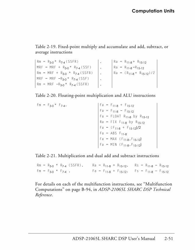
ADSP-21065L SHARC DSP User’s Manual 2-51
Computation Units
For details on each of the multifunction instructions, see “Multifunction Computations” on page B-94, in ADSP-21065L SHARC DSP Technical Reference.
Table 2-19. Fixed-point multiply and accumulate and add, subtract, or average instructions
Rm = R3-0 * R7-4 (SSFR) , Ra = R11-8 + R15-12
MRF = MRF + R3-0 * R7-4 (SSF) , Ra = R11-8 −R15-12
Rm = MRF + R3-0 * R7-4 (SSFR) , Ra = (R11-8 + R15-12)/2
MRF = MRF −R3-0 * R7-4 (SSF) ,
Rm = MRF −R3-0 * R7-4 (SSFR) ,
Table 2-20. Floating-point multiplication and ALU instructions
Fm = F3-0 * F7-4, Fa = F11-8 + F15-12
Fa = F11-8 − F15-12
Fa = FLOAT R11-8 by R15-12
Ra = FIX F11-8 by R15-12
Fa = (F11-8 + F15-12)/2Fa = ABS F11-8
Fa = MAX (F11-8,F15-12)Fa = MIN (F11-8,F15-12)
Table 2-21. Multiplication and dual add and subtract instructions
Rm = R3-0 * R7-4 (SSFR), Ra = R11-8 + R15-12, Rs = R11-8 − R15-12
Fm = F3-0 * F7-4 , Fa = F11-8 + F15-12, Fs = F11-8 − F15-12

Multifunction Operations
2-52 ADSP-21065L SHARC DSP User’s Manual
Figure 2-9. Input registers for multifunction computations (ALU and Multiplier)
R0—F0
R1—F1
R2—F2
R3—F3
R8—F8
R9—F9
R10—F10
R11—F11
R12—F12
R13—F13
R14—F14
R15—F15
R4—F4
R5—F5
R6—F6
R7—F7
Multiplier
ALU
Any Register
Any Register

ADSP-21065L SHARC DSP User’s Manual 3-1
3 PROGRAM SEQUENCINGFigure 3-0.
Table 3-0.
Listing 3-0.
The processor executes program instructions sequentially, in a linear flow, unless otherwise directed by various program structures:
• Loops
Execute one sequence of instructions several times, incurring zero overhead.
• Subroutines
Temporarily interrupt sequential flow to execute instructions from another part of program memory.
• Jumps
Permanently transfer program flow to another part of program memory.
• Interrupts
A special type of subroutine in which an event that happens at run time, not a program instruction, triggers the execution of the rou-tine.
• Idle
A special instruction that causes the processor to stop operations and hold its current state. When an interrupt occurs, the processor services the interrupt and continues normal execution.

3-2 ADSP-21065L SHARC DSP User’s Manual
Figure 3-1 on page 3-3 illustrates the variations in program flow that these program structures invoke.
To manage these program structures and the sequence of program flow, the core’s Program Sequencer:
• Selects the address of the next instruction, generating most of the addresses itself.
• Increments the fetch address.
• Maintains stacks.
• Evaluates conditions.
• Decrements the loop counter.
• Calculates new addresses.
• Maintains an instruction cache.
• Handles interrupts.
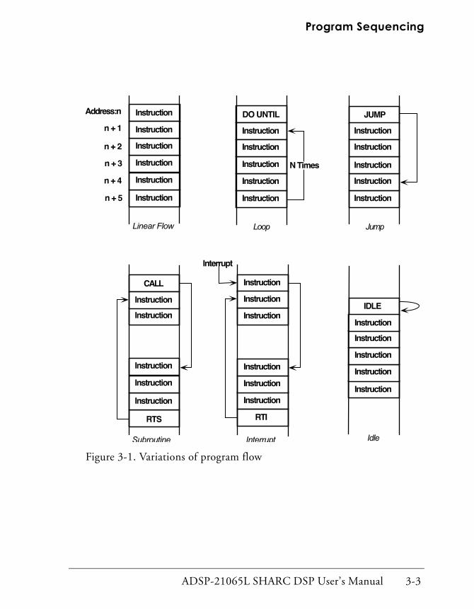
ADSP-21065L SHARC DSP User’s Manual 3-3
Program Sequencing
Figure 3-1. Variations of program flow
!
"
#
$%!!
%&
'
'(
')
'
'
*+
!,
-
Instruction Cycle
3-4 ADSP-21065L SHARC DSP User’s Manual
Instruction CycleThe ADSP-21065L processes instructions in three clock cycles:
• Fetch cycle
The processor reads the instruction from either the on-chip instruc-tion cache or from program memory.
• Decode cycle
The processor decodes the instruction, which generates conditions that control instruction execution.
• Execute cycle
The processor executes the instruction, completing the operations the instruction specified.
These cycles are overlapping, or pipelined, as shown in Table 3-1 on page 3-5. In sequential program flow, while the core is fetching one instruction, it is decoding the instruction it fetched in the previous cycle
When processing instructions, the processor uses its core clock, which runs at 2xCLKIN. Hereafter, in this chap-ter, all clock cycle references are to 2xCLKIN, unless oth-erwise noted.

ADSP-21065L SHARC DSP User’s Manual 3-5
Program Sequencing
and executing the instruction it fetched in the previous two cycles. Thus, throughput is one instruction per cycle.
Any nonsequential program flow can potentially decrease the processor’s instruction throughput. Nonsequential program operations include:
• Program memory data accesses that conflict with instruction fetches
• Jumps
• Subroutine calls and returns
• Interrupts and returns
• Loops
Table 3-1. Pipelined execution cycles
Time Instruction Sequence
(Cycles) Fetch Decode Execute
0 0x04
1 0x05 0x04
2 0x06 0x05 0x04
3 0x07 0x06 0x05
4 0x08 0x07 0x06

Program Sequencer Architecture
3-6 ADSP-21065L SHARC DSP User’s Manual
Program Sequencer ArchitectureFigure 3-2 shows the architecture of the Program Sequencer.
Figure 3-2. Block diagram of the Program Sequencer
The Program Sequencer selects the value of the next fetch address from several possible sources.
The fetch address register, decode address register, and program counter (PC) contain the addresses of the instructions the processor’s core is cur-rently fetching, decoding, and executing, respectively.
Applications use the PC stack in conjunction with the PC to store return addresses and top-of-loop addresses.
Loop AddressStack
Loop CountStack
LoopController
InterruptLatch
InterruptMask
InterruptMask Pointer
InterruptController
ProgramCounter
DecodeAddress
FetchAddress
ConditionLogic
InstructionCache
StatusStack
ASTAT MODE1
Instruction Latch
+DAG2
PCStack
+1
Next Address Multiplexer
InputFlags
InterruptVectorReturn Address
orTop of Loop
DirectBranch
PC-RelativeAddress
Internal PMD Bus
Loop Logic
IndirectBranch
Interrupts
Interrupt Logic
PMA Bus

ADSP-21065L SHARC DSP User’s Manual 3-7
Program Sequencing
The interrupt controller performs all functions related to interrupt pro-cessing, such as determining whether an interrupt is masked and generating the appropriate interrupt vector address.
The instruction cache enables the processor to access data in program memory and fetch an instruction (from the cache) in the same cycle. The DAG2 data address generator outputs program memory data addresses (for details, see Chapter 4, Data Addressing).
Using information from the status registers, the Program Sequencer evalu-ates conditional instructions and loop termination conditions.
The loop address stack and loop counter stack support nested loops.
The status stack stores status registers that provide support for implement-ing nested interrupt routines.
Program Sequencer and System RegistersTable 3-2 on page 3-8 lists the registers located in the Program Sequencer.
All registers in the Program Sequencer are universal registers, so they are accessible to other universal registers and to data memory. All registers and the tops of stacks are readable. All registers, except the fetch address, decode address, and PC, are writable.
Applications can write (and read) the PC stack pointer to push and pop the PC stack. Applications must issue explicit instructions to push or pop the loop address stack and the status stack.
Applications can use the System Register Bit Manipulation instruction to set, clear, toggle, or test specific bits in the system registers. For details, see Appendix A, Instruction Set Reference, in ADSP-21065L SHARC DSP Technical Reference.

Program Sequencer Architecture
3-8 ADSP-21065L SHARC DSP User’s Manual
Due to pipelining, writes to some of these registers do not take effect on the next cycle. For example, if you write the MODE1 register to enable ALU saturation mode, the change occurs two cycles after the write.
Some registers are not updated on the cycle immediately following a write; that is, an extra cycle occurs before a read of the register yields the new value. Table 3-2 and Table 3-3 on page 3-9 summarize the number of extra cycles that occur before a write takes effect (effect latency) and before a new value appears in the register (read latency) for Program Sequencer and system registers, respectively. A 0 indicates that the write takes effect or appears in the register on the next cycle after the write instruction exe-cutes. A 1 indicates one extra cycle.
Table 3-2. Program Sequencer registers read and effect latencies
Register Contents Bits Read Latency
Effect latency
FADDR fetch address 24 — —
DADDR decode address 24 — —
PC execute address 24 — —
PCSTK top of PC stack 24 0 0
PCSTKP PC stack pointer 5 1 1
LADDER top of loop address stack
32 0 0
CURLCNTR top of loop count stack (current loop count)
32 0 0
LCNTR loop count for next DO UNTIL loop
32 0 0
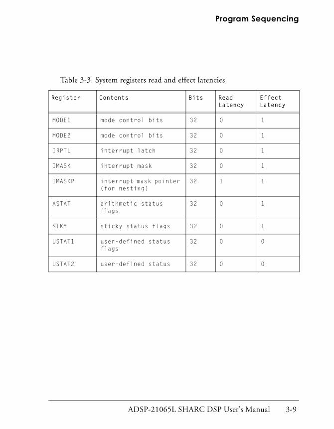
ADSP-21065L SHARC DSP User’s Manual 3-9
Program Sequencing
Table 3-3. System registers read and effect latencies
Register Contents Bits Read Latency
Effect Latency
MODE1 mode control bits 32 0 1
MODE2 mode control bits 32 0 1
IRPTL interrupt latch 32 0 1
IMASK interrupt mask 32 0 1
IMASKP interrupt mask pointer (for nesting)
32 1 1
ASTAT arithmetic status flags
32 0 1
STKY sticky status flags 32 0 1
USTAT1 user-defined status flags
32 0 0
USTAT2 user-defined status 32 0 0
Program Sequencer Operation
3-10 ADSP-21065L SHARC DSP User’s Manual
Program Sequencer OperationThis section describes how the Program Sequencer operates and defines the various kinds of program flow it supports.
Sequential Program FlowTo determine the next instruction address, the Program Sequencer exam-ines both the instruction currently executing and the current state of the processor. Unless it encounters a program structure that alters program flow, the Program Sequencer simply increments the fetch address to exe-cute instructions from program memory in sequential order.
Program Memory Data AccessesUsually, the processor’s core fetches an instruction from memory on each cycle. When the processor executes an instruction that requires it to read or write data to the same memory block that contains the instruction, the fetch causes a conflict for access to the block. To reduce delays such con-flicts cause, the processor uses its instruction cache.
The first time the processor encounters an instruction fetch that conflicts with a program memory data access, it must wait to fetch the instruction on the following cycle, causing a delay. To prevent the same delay from reoccurring, the processor automatically writes the fetched instruction to the instruction cache. The processor checks the instruction cache on every program memory data access. If the needed instruction is in the cache, the fetch from the cache occurs in parallel with the access to program memory data, avoiding a delay.

ADSP-21065L SHARC DSP User’s Manual 3-11
Program Sequencing
BranchesA branch occurs when the current fetch address does not follow the previ-ous fetch address sequentially. The processor supports jumps, calls, and returns.
In the Program Sequencer, a jump differs from a call only in that:
• Calls branch to a new location, but upon execution, the Program Sequencer pushes onto the PC stack a return address, which is avail-able when the processor executes a return instruction later.
• Jumps branch to a new location permanently and do not provide for a return.
LoopsThe processor supports program loops with the DO UNTIL instruction. The DO UNTIL instruction causes the processor to repeat a sequence of instructions until a specified condition tests true.
Executing Conditional Instructions
3-12 ADSP-21065L SHARC DSP User’s Manual
Executing Conditional InstructionsThe Program Sequencer evaluates conditions to determine whether to exe-cute a conditional instruction and when to terminate a loop. The conditions are based on information from the arithmetic status (ASTAT) register, mode control 1 (MODE1) register, flag inputs, and loop counter. See Chapter 2, Computation Units, for a description of the arithmetic ASTAT bits.
Each condition that the Program Sequencer evaluates has an assembler mnemonic and a unique code, used in a conditional instruction’s opcode. For most conditions, the Program Sequencer can test both true and false states (=0 and ≠0). Table 3-4 on page 3-13 defines the processor’s thirty-two condition and termination codes.
After it is set, applications can use the bit test flag (BTF), bit 18 of the ASTAT register, as the condition in a conditional instruction (with the mnemonic TF, see Table 3-4). The results of the BIT TST and BIT XOR forms of the System Register Bit Manipulation instruction, which applica-tions can use to test the contents of the processor’s system registers, set and clear this flag. For details, see Appendix A, Instruction Set Reference, in ADSP-21065L SHARC DSP Technical Reference.
The two conditions that lack complements are LCE/NOT LCE (loop counter expired/not expired) and TRUE/FOREVER. Context determines the interpretation of these condition codes. You use TRUE and NOT LCE in conditional instructions and FOREVER and LCE in loop termi-nation instructions.
The IF TRUE construct creates an unconditional instruction (the same effect as leaving out the condition entirely). A DO FOREVER instruction executes a loop indefinitely, until an interrupt or reset intervenes.
Applications typically use the LCE condition (loop counter expired) in DO UNTIL instructions. Because the LCE condition checks the value of the loop counter (CURLCNTR), avoid following a write from memory to
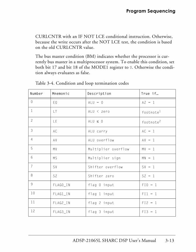
ADSP-21065L SHARC DSP User’s Manual 3-13
Program Sequencing
CURLCNTR with an IF NOT LCE conditional instruction. Otherwise, because the write occurs after the NOT LCE test, the condition is based on the old CURLCNTR value.
The bus master condition (BM) indicates whether the processor is cur-rently bus master in a multiprocessor system. To enable this condition, set both bit 17 and bit 18 of the MODE1 register to 0. Otherwise the condi-tion always evaluates as false.
Table 3-4. Condition and loop termination codes
Number Mnemonic Description True if…
0 EQ ALU = 0 AZ = 1
1 LT ALU < zero footnote1
2 LE ALU ≤ 0 footnote2
3 AC ALU carry AC = 1
4 AV ALU overflow AV = 1
5 MV Multiplier overflow MV = 1
6 MS Multiplier sign MN = 1
7 SV Shifter overflow SV = 1
8 SZ Shifter zero SZ = 1
9 FLAG0_IN flag 0 input FI0 = 1
10 FLAG1_IN flag 1 input FI1 = 1
11 FLAG2_IN flag 2 input FI2 = 1
12 FLAG3_IN flag 3 input FI3 = 1
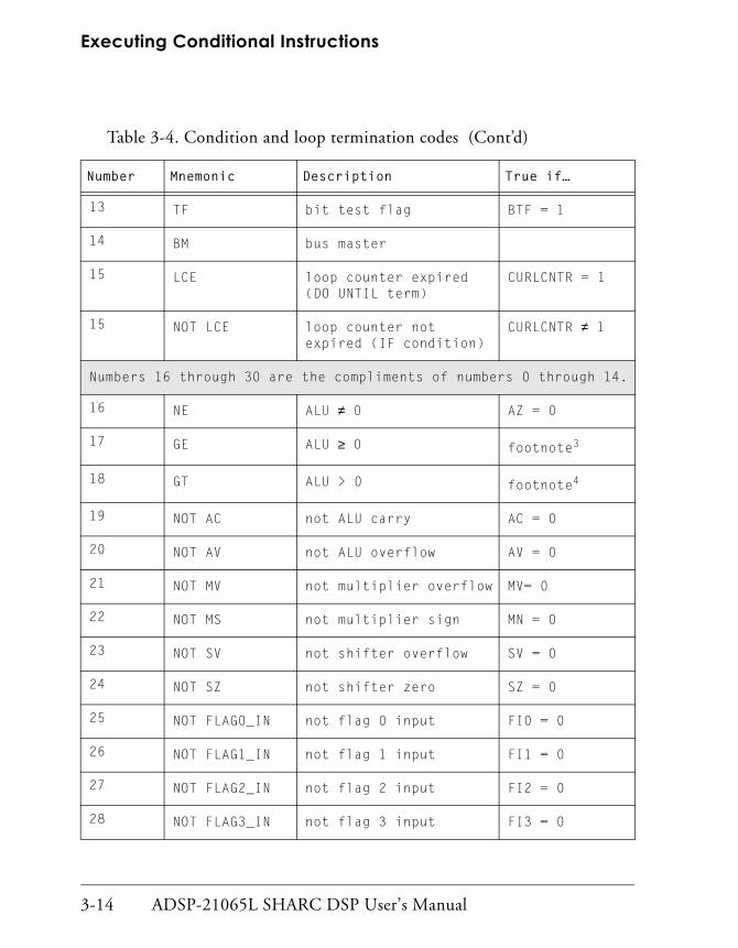
Executing Conditional Instructions
3-14 ADSP-21065L SHARC DSP User’s Manual
13 TF bit test flag BTF = 1
14 BM bus master
15 LCE loop counter expired(DO UNTIL term)
CURLCNTR = 1
15 NOT LCE loop counter not expired (IF condition)
CURLCNTR ≠ 1
Numbers 16 through 30 are the compliments of numbers 0 through 14.
16 NE ALU ≠ 0 AZ = 0
17 GE ALU ≥ 0 footnote3
18 GT ALU > 0 footnote4
19 NOT AC not ALU carry AC = 0
20 NOT AV not ALU overflow AV = 0
21 NOT MV not multiplier overflow MV= 0
22 NOT MS not multiplier sign MN = 0
23 NOT SV not shifter overflow SV = 0
24 NOT SZ not shifter zero SZ = 0
25 NOT FLAG0_IN not flag 0 input FI0 = 0
26 NOT FLAG1_IN not flag 1 input FI1 = 0
27 NOT FLAG2_IN not flag 2 input FI2 = 0
28 NOT FLAG3_IN not flag 3 input FI3 = 0
Table 3-4. Condition and loop termination codes (Cont’d)
Number Mnemonic Description True if…
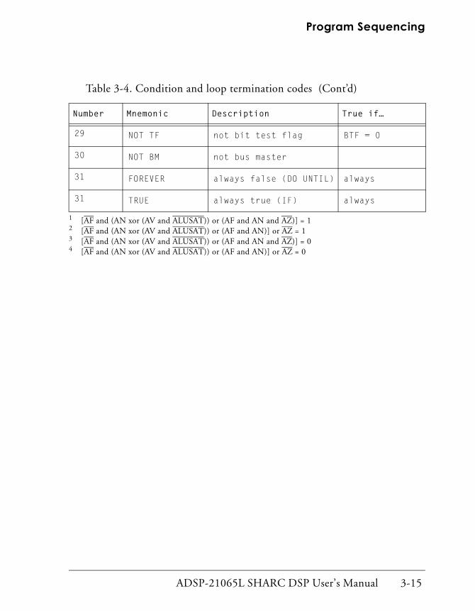
ADSP-21065L SHARC DSP User’s Manual 3-15
Program Sequencing
29 NOT TF not bit test flag BTF = 0
30 NOT BM not bus master
31 FOREVER always false (DO UNTIL) always
31 TRUE always true (IF) always
1 [AF and (AN xor (AV and ALUSAT)) or (AF and AN and AZ)] = 12 [AF and (AN xor (AV and ALUSAT)) or (AF and AN)] or AZ = 13 [AF and (AN xor (AV and ALUSAT)) or (AF and AN and AZ)] = 04 [AF and (AN xor (AV and ALUSAT)) or (AF and AN)] or AZ = 0
Table 3-4. Condition and loop termination codes (Cont’d)
Number Mnemonic Description True if…

Branches (call, jump, rts, rti)
3-16 ADSP-21065L SHARC DSP User’s Manual
Branches (call, jump, rts, rti)The CALL instruction initiates a subroutine. Both jumps and calls trans-fer program flow to another memory location, but a call also pushes a return address onto the PC stack, so it is available when a return from sub-routine instruction is later executed. Jumps branch to a new location, with no provision for return.
A return causes the processor to branch to the address stored at the top of the PC stack.
Returns are of two types:
• Return from subroutine (RTS)
• Return from interrupt (RTI)
Both instructions pop the return address off the PC stack, but the RTI instruction also:
• Pops the status stack if the ASTAT and MODE1 status registers have been pushed (if the interrupt was IRQ2-0, the timer interrupt, or the VIRPT vector interrupt).
• Clears the appropriate bit in the interrupt latch register (IRPTL) and the interrupt mask pointer (IMASKP).
You can specify a number of parameters for branches:
• Jumps, calls and returns can be conditional.
The Program Sequencer can evaluate any one of several status con-ditions to determine whether to take the branch. If no condition is specified, it always takes the branch.
ADSP-21065L SHARC DSP User’s Manual 3-17
Program Sequencing
• Jumps and calls can be indirect, direct, or PC-relative.
An indirect branch goes to an address that DAG2, one of the data address generators, supplies.
Direct branches jump to the 24-bit address that an immediate field in the branch instruction specifies.
PC-relative branches also use a value that the instruction specifies, but the Program Sequencer adds this value to the current PC value to compute the destination address.
• Jumps, calls and returns can be delayed or nondelayed.
In a delayed branch, the processor executes the two instructions that immediately follow the branch instruction.
In a nondelayed branch, the Program Sequencer suppresses the exe-cution of the two immediately following instructions, so the proces-sor executes NOPs instead.
• If it occurs inside a loop, the JUMP (LA) instruction causes an auto-matic loop abort.
When the loop aborts, the Program Sequencer pops the PC and loop address stacks once, so if the aborted loop was nested, the stacks still contain the correct values for the outer loop.
JUMP (LA) is similar to the C programming language’s break instruction, which prematurely terminates execution of a loop.
You cannot use JUMP (LA) in the last three instructions of a loop.

Branches (call, jump, rts, rti)
3-18 ADSP-21065L SHARC DSP User’s Manual
Delayed and Nondelayed BranchesAn instruction modifier DB indicates that a branch is delayed; otherwise, it is nondelayed.
If the branch is nondelayed, the processor does not execute the two instructions after the branch, which are in the fetch and decode stages (see Table 3-5 and Table 3-6). For a call, the decode address (the address of the instruction after the call) is the return address. During the two NOP cycles, the processor fetches and decodes the first instruction at the branch address.
Table 3-5. Nondelayed jump or call
Pipeline CLK1 CLK2 CLK3 CLK4
Execute n NOP NOP j
Decode n+1→nop n+2→nop j j+1
Fetch n+2 j j+1 j+2
n+1 suppressed n+2 suppressed; for call, n+1 pushed on PC stack
n = Branch instruction; j = Instruction at jump or call address
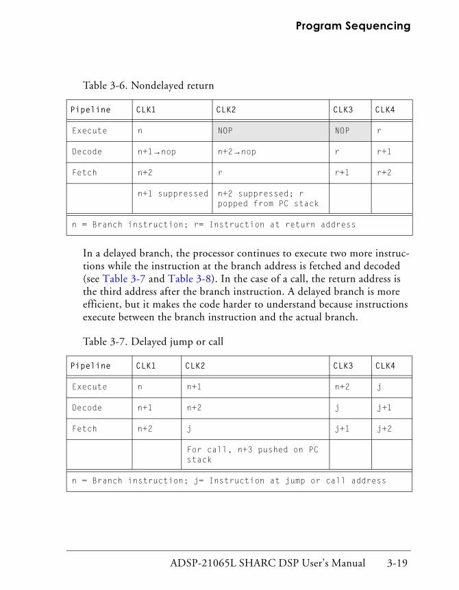
ADSP-21065L SHARC DSP User’s Manual 3-19
Program Sequencing
In a delayed branch, the processor continues to execute two more instruc-tions while the instruction at the branch address is fetched and decoded (see Table 3-7 and Table 3-8). In the case of a call, the return address is the third address after the branch instruction. A delayed branch is more efficient, but it makes the code harder to understand because instructions execute between the branch instruction and the actual branch.
Table 3-6. Nondelayed return
Pipeline CLK1 CLK2 CLK3 CLK4
Execute n NOP NOP r
Decode n+1→nop n+2→nop r r+1
Fetch n+2 r r+1 r+2
n+1 suppressed n+2 suppressed; r popped from PC stack
n = Branch instruction; r= Instruction at return address
Table 3-7. Delayed jump or call
Pipeline CLK1 CLK2 CLK3 CLK4
Execute n n+1 n+2 j
Decode n+1 n+2 j j+1
Fetch n+2 j j+1 j+2
For call, n+3 pushed on PC stack
n = Branch instruction; j= Instruction at jump or call address

Branches (call, jump, rts, rti)
3-20 ADSP-21065L SHARC DSP User’s Manual
Because of the instruction pipeline, the processor must execute sequen-tially a delayed branch instruction and the two instructions that follow it. None of the following instructions can occupy the two locations immedi-ately following a delayed branch instruction.
• PUSH and POP of the PC STACK: Push of the PC stack in the delayed branch should be followed by a pop. A value that is pushed in the delay branch of the call should be popped first in the called subroutine. The pop should then be followed by a return to subroutine “rts.” Consider the following example.
20119 call foo (db);2011A push PCSTK;2011B nop;2011C foo;
PCSTK 2011B - 2nd push due to PCSTK.2011C -1st push due to call.
This example shows that when you push the PCSTK during a delay slot, the PC stack pointer is pushed onto the PCSTK.
Table 3-8. Delayed return
Pipeline CLK1 CLK2 CLK3 CLK4
Execute n n+1 n+2 r
Decode n+1 n+2 r r+1
Fetch n+2 r r+1 r+2
r popped from PC stack
n = Branch instruction; r= Instruction at return address

ADSP-21065L SHARC DSP User’s Manual 3-21
Program Sequencing
Now you have to execute the following instruction before doing an “rts.”
pop PCSTK;rts(db);nop;nop;
If you do a push of a PC stack, you have to do a pop first and then an “rts.” If a value is popped inside the delay branch, the return address of the pushed subroutine is popped back and is, therefore, restricted.
• DO UNTIL: A loop that is inside the delay branch does a sequential operation after executing the loop and does not jump to the label. The reason is because running a loop in a delay branch flushes the destination address of the jump address out of the pipeline. Instead of the fetch, decode and execute stages in the pipeline, the loop instructions are in the pipeline and the operation is sequential thereafter. Look at the following example.
20118 LCNTR =10;20119 jump my(db); 2012C my:2011A do myl until LCE;2011B myl:r0 =r0 +r1;
2011C r2=r2+r3;2011D r1 =r1 +r2;
This example shows a loop inside a delay branch. Since the loop exe-cutes the instructions inside the loop 10 times, the address of the jump (2012C) destination is flushed. Therefore, instead of going to label “my” (2012C), the processor executes the next sequential instruction at address 2011C and then continues the sequential exe-cution. For this reason, the loop is restricted inside the delay branch.
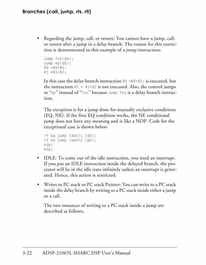
Branches (call, jump, rts, rti)
3-22 ADSP-21065L SHARC DSP User’s Manual
• Regarding the jump, call, or return: You cannot have a jump, call, or return after a jump in a delay branch. The reason for this restric-tion is demonstrated in this example of a jump instruction:
Jump foo(db);Jump my(db);R0 =R0+R1;R1 =R1+R2;
In this case the delay branch instruction R0 =R0+R1; is executed, but the instruction R1 = R1+R2 is not executed. Also, the control jumps to “my” instead of “foo” because Jump foo is a delay branch instruc-tion.
The exception is for a jump done for mutually exclusive conditions (EQ, NE). If the first EQ condition works, the NE conditional jump does not have any meaning and is like a NOP. Code for the exceptional case is shown below:
if eq jump label1 (db);if ne jump label2 (db);nop;nop;
• IDLE: To come out of the idle instruction, you need an interrupt. If you put an IDLE instruction inside the delayed branch, the pro-cessor will be in the idle state infinitely unless an interrupt is gener-ated. Hence, this action is restricted.
• Writes to PC stack or PC stack Pointer: You can write to a PC stack inside the delay branch by writing to a PC stack inside either a jump or a call.
The two instances of writing to a PC stack inside a jump are described as follows.

ADSP-21065L SHARC DSP User’s Manual 3-23
Program Sequencing
a. The PC stack has a value – When the PC stack already has a value and you write a value onto the PC stack, the value already in the PC stack is overwritten by the value written onto the PC stack. Since the value in the PC stack is corrupted, this action is restricted.
b. The PC stack is empty – When you write a value onto an empty PC stack, the PC stack will be empty even after you write the value onto the PC stack.
If you write to a PC stack inside a call, the value that is pushed onto the PC stack because of the call is overwritten by the value written onto the PC stack. Hence, when you do an “rts,” you return to the address that you had written onto the PC stack, not the address that you had pushed while branching to the subroutine. The explanation is shown in this example:
20111 call foo3(db);20112 PCSTK=0x2011C;20113 nop;20114
The value 20114 is pushed onto the PC stack. Since you are also writing the value 2011C to the PC stack, the value 20114 is overwritten by 2011C in the PC stack. When you come back by doing a “rts,” you return to the address 2011C, not to 20114. Therefore, this action is restricted.
The ADSP-21000 Family assembler checks for these exceptions.
Since the processor must execute a delayed branch instruction and the two following instructions sequentially, it does not process interrupts between execution of these instructions. The processor latches any interrupt that occurs during these instructions but does not process them until it exe-cutes the branch.

Branches (call, jump, rts, rti)
3-24 ADSP-21065L SHARC DSP User’s Manual
You can read the PC stack or PC stack pointer immediately after a delayed call or return, but the result will indicate that the return address on the PC stack has been pushed or popped, even though the branch has not actually occurred.
PC StackThe PC stack holds return addresses for subroutines, interrupt service rou-tines, and top-of-loop addresses for loops. The PC stack is thirty locations deep by 24-bits wide.
The Program Sequencer pops the PC stack during returns from interrupts (RTI), returns from subroutines (RTS), and terminations of loops. The stack is full when all entries are occupied; empty when no entries are occu-pied; and has overflowed if a call occurs when the stack is already full.
The sticky status register (STKY) stores the full and empty flags. The full flag causes a maskable interrupt.
A PC stack interrupt occurs when twenty-nine locations in the PC stack are filled (the almost full state). Entering the interrupt service routine then immediately causes a push on the PC stack, making it full. So, the inter-rupt is a stack full interrupt, even though the condition that triggers it is the almost full condition. The other stacks in the Program Sequencer, the loop address stack, loop counter stack, and status stack, are provided with overflow interrupts that are activated when a push occurs while the stack is in a full state.
The program counter stack pointer (PCSTKP) is a readable and writable register that contains the address of the top of the PC stack. The value of PCSTKP is 0 when the PC stack is empty; 1, 2,..., 30 when the stack con-tains data; and 31 when the stack has overflowed. A write to PCSTKP takes effect after a one-cycle delay. If the PC stack has overflowed, a write to PCSTKP has no effect.

ADSP-21065L SHARC DSP User’s Manual 3-25
Program Sequencing
Loops (DO UNTIL)The DO UNTIL instruction provides for efficient software loops, without the overhead of additional instructions to branch, test a condition, or dec-rement a counter.
A simple example of a loop looks like this:
LCNTR=30, DO label UNTIL LCE;R0=DM(I0,M0), F2=PM(I8,M8);R1=R0-R15;
label: F4=F2+F3;
When the processor executes a DO UNTIL instruction, the Program Sequencer pushes the address of the last loop instruction and the termina-tion condition for exiting the loop (both specified in the instruction) onto the loop address stack. It also pushes the top-of-loop address, which is the address of the instruction following the DO UNTIL instruction, onto the PC stack.
Because of the instruction pipeline—the fetch, decode, and execute cycles—the processor tests the termination condition before the end of the loop, so the next fetch either exits the loop or returns to the top. (If the loop is counter-based, the Program Sequencer decrements the counter.) Specifically, the Program Sequencer tests the condition when the instruc-tion two locations before the last instruction in the loop executes. (The last instruction resides at location e −2, where e is the end-of-loop address.) If the termination condition is false, the processor fetches the instruction from the top-of-loop address stored on the top of the PC stack. If the termination condition is true, the processor fetches the next

Loops (DO UNTIL)
3-26 ADSP-21065L SHARC DSP User’s Manual
instruction after the end of the loop and pops the loop stack and PC stack. Table 3-9 and Table 3-10 show these loop operations.
Table 3-9. Loop-Back
Pipeline CLK1 CLK2 CLK3 CLK4
Execute e −2 e −1 e b
Decode e −1 e b b+1
Fetch e b b+1 b+2
Termination con-dition tests false
Loop start address is top of PC stack
e = Loop end instruction; b = Loop start instruction
Table 3-10. Loop termination
Pipeline CLK1 CLK2 CLK3 CLK4
Execute e −2 e −1 e e+1
Decode e −1 e e+1 e+2
Fetch e e+1 e+2 e+3
Termination con-dition tests true
Loopback aborts; PC and loop stacks popped
e = Loop end instruction; b = Loop start instruction

ADSP-21065L SHARC DSP User’s Manual 3-27
Program Sequencing
Restrictions and Short LoopsThis section describes several programming restrictions placed on loops, and it explains restrictions that result from the three-instruction, fetch-decode-execute pipeline and restrictions that apply specifically to short loops of one and two instructions.
General Restrictions
• Nested loops cannot terminate on the same instruction.
• The last three instructions of a loop cannot be a branch (jump, call, or return).
This restriction also applies to one-instruction loops and two-instruction loops with only one iteration.
This rule has one exception—a nondelayed CALL (no DB modifier) paired with an RTS (LR) return from subroutine with loop reentry modifier. You can use the nondelayed CALL as one of the last three instructions of a loop (except in a one-instruction loop or a two-instruction, single-iteration loop.)
The RTS (LR) instruction ensures proper reentry into a loop. In counter-based loops, for example, to check the termination condi-tion, you decrement the current loop counter (CURLCNTR) while the instruction two locations before the end of the loop is executing. You can then use a nondelayed CALL in one of the last two loca-tions, providing you use an RTS (LR) instruction to return from the subroutine.
The loop reentry (LR) modifier assures proper reentry into the loop by preventing the loop counter from being decremented again (that is, twice for the same loop iteration).
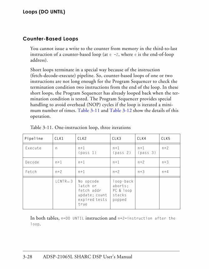
Loops (DO UNTIL)
3-28 ADSP-21065L SHARC DSP User’s Manual
Counter-Based Loops
You cannot issue a write to the counter from memory in the third-to-last instruction of a counter-based loop (at e −2, where e is the end-of-loop address).
Short loops terminate in a special way because of the instruction (fetch-decode-execute) pipeline. So, counter-based loops of one or two instructions are not long enough for the Program Sequencer to check the termination condition two instructions from the end of the loop. In these short loops, the Program Sequencer has already looped back when the ter-mination condition is tested. The Program Sequencer provides special handling to avoid overhead (NOP) cycles if the loop is iterated a mini-mum number of times. Table 3-11 and Table 3-12 show the details of this operation.
In both tables, n=DO UNTIL instruction and n+2=instruction after the loop.
Table 3-11. One-instruction loop, three iterations
Pipeline CLK1 CLK2 CLK3 CLK4 CLK5
Execute n n+1(pass 1)
n+1(pass 2)
n+1(pass 3)
n+2
Decode n+1 n+1 n+1 n+2 n+3
Fetch n+2 n+1 n+2 n+3 n+4
LCNTR←3 No opcode latch or fetch addr update; count expired tests true
loop-backaborts; PC & loop stacks popped

ADSP-21065L SHARC DSP User’s Manual 3-29
Program Sequencing
For no overhead, the processor must execute a loop of length one at least three times and a loop of length two at least twice.
Loops of length one that iterate only once or twice and loops of length two that iterate only once incur two cycles of overhead because of the two aborted instructions after the last iteration to clear the instruction pipeline.
Processing of an interrupt that occurs during the last iteration of a one-instruction loop that executes once or twice, a two-instruction loop that executes once, or the cycle following one of these loops (which is a NOP) is delayed one cycle. Similarly, in a one-instruction loop that exe-cutes at least three times (three nitrations), processing is delayed one cycle if the interrupt occurs during the third-to-last iteration.
Noncounter-Based Loops
A noncounter-based loop is one in which the loop termination condition is something other than LCE. When a noncounter-based loop is the outer
Table 3-12. One-instruction loop, two iterations (overhead = 2 cycles)
Pipeline CLK1 CLK2 CLK3 CLK4 CLK5 CLK6
Execute n n+1(pass 1)
n+1(pass 2)
NOP NOP n+2
Decode n+1 n+1 n+1→nop n+1→nop n+2 n+3
Fetch n+2 n+1 n+1 n+2 n+3 n+4
LCNTR←2 No opcode latch or fetch addr update
Count expired tests true
loop-backaborts; PC & loop stacks popped
Loops (DO UNTIL)
3-30 ADSP-21065L SHARC DSP User’s Manual
loop in a series of nested loops, the end address of the outer loop must be located at least two addresses after the end address of the inner loop.
To abort execution of a loop prematurely, use the JUMP (LA) instruction. When this instruction is located in the inner loop of a series of nested loops, and the outer loop is noncounter-based, the address the program jumps to cannot be the outer loop’s last instruction. It can, however, be the next-to-last instruction (or any earlier instruction).
Noncounter-based short loops terminate in a special way because of the instruction pipeline (fetch-decode-execute):
• In a three-instruction loop, the Program Sequencer tests the termi-nation condition when the processor executes the top-of-loop instruction.
When the condition becomes true, the Program Sequencer com-pletes one full pass of the loop before exiting it.
• In a two-instruction loop, the termination condition is checked dur-ing the last (second) instruction. See Table 3-13 and Table 3-14 on page 3-31 and page 3-32, respectively.
If the condition becomes true when the first instruction is executed, it tests true during the second, and the Program Sequencer com-pletes one more full pass before exiting the loop.
If the condition becomes true during the second instruction, how-ever, the Program Sequencer completes two more full passes before exiting the loop.
In a one-instruction loop, the termination condition is checked every cycle. When the condition becomes true, the Program Sequencer executes the loop three more times before exiting it.

ADSP-21065L SHARC DSP User’s Manual 3-31
Program Sequencing
In both examples, n=DO UNTIL instruction and n+3=instruction after the loop.
Table 3-13. Two-instruction loop, two iterations
Pipeline CLK1 CLK2 CLK3 CLK4 CLK5 CLK6
Execute n n+1(pass1)
n+2(pass1)
n+1(pass2)
n+2(pass2)
n+3
Decode n+1 n+2 n+1 n+2 n+3 n+4
Fetch n+2 n+1 n+2 n+3 n+4 n+5
LCNTR←2 PC stack sup-plies loop start addr
last fetch causes cond. test; tests true
Loop-back-aborts; PC & loop stacks popped
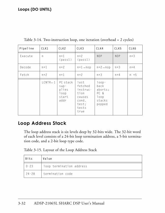
Loops (DO UNTIL)
3-32 ADSP-21065L SHARC DSP User’s Manual
Loop Address StackThe loop address stack is six levels deep by 32-bits wide. The 32-bit word of each level consists of a 24-bit loop termination address, a 5-bit termina-tion code, and a 2-bit loop type code.
Table 3-14. Two-instruction loop, one iteration (overhead = 2 cycles)
Pipeline CLK1 CLK2 CLK3 CLK4 CLK5 CLK6
Execute n n+1(pass1)
n+2(pass1)
NOP NOP n+3
Decode n+1 n+2 n+1→nop n+2→nop n+3 n+4
Fetch n+2 n+1 n+2 n+3 n+4 n +5
LCNTR←1 PC stack sup-plies loop start addr
last fetched instruc-tion causes cond. test; tests true
loop-back aborts; PC & loop stacks popped
Table 3-15. Layout of the Loop Address Stack
Bits Value
0-23 loop termination address
24-28 termination code

ADSP-21065L SHARC DSP User’s Manual 3-33
Program Sequencing
The processor stacks the loop termination address, termination code, and loop type code when it executes a DO UNTIL or a PUSH LOOP instruc-tion. It pops the stack two instructions before the end of the last loop iteration or when it executes a POP LOOP instruction. A stack overflows if a push occurs when all entries in the loop stack are occupied. The stack is empty when no entries are occupied. The sticky status register (STKY) contains the overflow and empty flags. Overflow causes a maskable interrupt.
The LADDR register contains the top of the loop address stack. It is read-able and writable over the DM Data bus. Reading and writing LADDR does not move the loop address stack pointer, but a stack push or pop, performed with explicit instructions, does move the stack pointer. LADDR contains the value 0xFFFF FFFF when the loop address stack is empty.
Because the Program Sequencer checks the termination condition two instructions before the end of the loop, it pops the loop stack before the end of the loop on the final iteration. If LADDR is read at either of these instructions, the value will no longer be the termination address for the loop.
29 reserved (always reads 0)
30-31 loop type code
00 = arithmetic condition-based (not LCE)
01 = counter-based, length 1
10 = counter-based, length 2
11 = counter-based, length > 2
Table 3-15. Layout of the Loop Address Stack (Cont’d)
Bits Value
Loops (DO UNTIL)
3-34 ADSP-21065L SHARC DSP User’s Manual
A jump out of a loop pops the loop address stack (and the loop count stack if the loop is counter-based) if the Loop Abort (LA) modifier is spec-ified for the jump. This action enables the loop mechanism to continue functioning correctly. Only one pop is performed, however, so you cannot use the loop abort to jump more than one level of nesting.
Loop Counters and StackThe loop counter stack is six levels deep by 32-bits wide. The loop counter stack works in synchronization with the loop address stack—both stacks always have the same number of locations occupied. So, the same empty and overflow status flags apply to both stacks.
The processor’s Program Sequencer operates two separate loop counters:
• The current loop counter (CURLCNTR)
Tracks iterations for an executing loop.
• The loop counter (LCNTR)
Holds the initial count value of the loop before it is executed. While setting up the count for an inner loop, two counters are needed to maintain the count for the outer loop.
The Current Loop Counter (CURLCNTR)
The top entry in the loop counter stack always contains the loop count currently in effect. This entry is the CURLCNTR register, which is read-able and writable over the DM Data bus. A read of CURLCNTR when the loop counter stack is empty gives the value 0xFFFF FFFF.
The Program Sequencer decrements the value of CURLCNTR for each loop iteration. Because it checks the termination condition two instruc-tion cycles before the end of the loop, the Program Sequencer also decrements the loop counter before the end of the loop. So, if you read

ADSP-21065L SHARC DSP User’s Manual 3-35
Program Sequencing
CURLCNTR at either of the last two loop instructions, the value read is the count for the next iteration.
The processor pops the loop counter stack two instructions before the end of the last loop iteration. When it does so, the new top entry of the stack becomes the CURLCNTR value, the count in effect for the executing loop. If no loop is executing, the value of CURLCNTR is 0xFFFF FFFF after the pop.
Writing CURLCNTR does not cause a stack push. So, if you write a new value to CURLCNTR, you change the count value of the loop currently executing. A write to CURLCNTR when no DO UNTIL LCE loop is executing has no effect.
Because the processor must use CURLCNTR to perform counter-based loops, some restrictions exist that determine when you can write CURL-CNTR. As mentioned earlier, you cannot issue a write to CURLCNTR from memory in the third-to-last instruction of a DO UNTIL LCE loop. You also cannot issue a write to CURLCNTR from memory in the instruction that follows an IF NOT LCE instruction.
The Loop Counter (LCNTR)
LCNTR is the value of the top of the loop counter stack plus one; that is, it is the location on the stack that takes effect on the next push of the loop stack. To set up a count value for a nested loop, without affecting the count value of the loop currently executing, you write the count value to
LCNTR. A value of 0 in LCNTR causes a loop to execute 232 times.
The DO UNTIL LCE instruction pushes the value of LCNTR on the loop count stack, so it becomes the new CURLCNTR value. Figure 3-3 on page 3-36 shows this process. The previous CURLCNTR value is pre-served one location down in the stack.

Loops (DO UNTIL)
3-36 ADSP-21065L SHARC DSP User’s Manual
Figure 3-3. Pushing the loop counter stack for nested loops
1. The processor is not executing a loop, and the loop counter stack is empty. The Program Sequencer loads LCNTR with aaaa aaaa.
2. The processor is executing a single loop. The Program Sequencer loads LCNTR with the value bbbb bbbb.
1
aaaa aaaa
0xFFFF FFFF
aaaa aaaa
LCNTR
CURLCNTR
LCNTR
CURLCNTR
LCNTR
3
aaaa aaaa
bbbb bbbb
cccc cccc
CURLCNTR
7
aaaa aaaa
bbbb bbbb
cccc cccc
dddd dddd
eeee eeee
ffff ffff
CURLCNTR
LCNTR
2
aaaa aaaa
bbbb bbbb
CURLCNTR
LCNTR
5
aaaa aaaa
bbbb bbbb
cccc cccc
dddd dddd
eeee eeee
CURLCNTR
LCNTR
CURLCNTR
LCNTR
6
aaaa aaaa
bbbb bbbb
cccc cccc
dddd dddd
eeee eeee
ffff ffff
4
aaaa aaaa
bbbb bbbb
cccc cccc
dddd dddd
ADSP-21065L SHARC DSP User’s Manual 3-37
Program Sequencing
3. The processor is executing two nested loops. The Program Sequencer loads LCNTR with the value cccc cccc.
4. The processor is executing three nested loops. The Program Sequencer loads LCNTR with the value dddd dddd.
5. The processor is executing four nested loops. The Program Sequencer loads LCNTR with the value eeee eeee.
6. The processor is executing five nested loops. The Program Sequencer loads LCNTR with the value ffff ffff.
7. The processor is executing six nested loops. The loop counter stack (LCNTR) is full.
A read of LCNTR when the loop counter stack is full results in invalid data. When the loop counter stack is full, the processor discards any data written to LCNTR.
If you read LCNTR during the last two instructions of a terminating loop, its value is the last CURLCNTR value for the loop.

Interrupts
3-38 ADSP-21065L SHARC DSP User’s Manual
InterruptsA variety of conditions, both internal and external to the processor, cause interrupts. An interrupt forces a subroutine call to a predefined address, the interrupt vector. The processor assigns a unique vector to each type of interrupt.
Externally, the processor supports three prioritized, individually maskable interrupts, each of which can be either level- or edge-triggered (MODE2 register). An external device asserting one of the processor’s interrupt inputs (IRQ2-0) causes these interrupts.
Arithmetic exceptions, stack overflows, and circular data buffer overflows are some of the internally-generated interrupts.
The processor deems an interrupt request valid if all of the following con-ditions are true:
• The request is not masked;
• Interrupts are globally enabled (IRPTEN=1);
• No higher-priority request is pending.
Valid requests invoke an interrupt service sequence that branches to the address reserved for that interrupt. Interrupt vectors are spaced at intervals of four instructions, but applications can branch to another region of memory to accommodate longer service routines. Program execution returns to normal sequencing when the processor executes an RTI (return from interrupt) instruction.
The processor cannot service an interrupt unless its core is executing instructions or is in the IDLE state. IDLE and IDLE16 are a special instructions that halt the processor’s core until an external interrupt or a timer interrupt occurs.
ADSP-21065L SHARC DSP User’s Manual 3-39
Program Sequencing
To process an interrupt, the processor’s Program Sequencer performs these actions:
1. Outputs the appropriate interrupt vector address.
2. Pushes the current PC value (the return address) on the PC stack.
If the interrupt is an external interrupt (IRQ2-0), the internal timer interrupt, or the VIRPT multiprocessor vector interrupt, the Pro-gram Sequencer pushes the current value of the ASTAT and MODE1 registers onto the status stack.
3. Sets the appropriate bit in the interrupt latch register (IRPTL).
4. Updates the interrupt mask pointer (IMASKP) to reflect the cur-rent interrupt nesting state.
The nesting mode (NESTM) bit in the MODE1 register deter-mines whether all interrupts or only lower priority interrupts are masked during the service routine.
At the end of the interrupt service routine, the RTI instruction causes the Program Sequencer to perform these actions:
1. Returns to the address stored at the top of the PC stack.
2. Pops this value off of the PC stack.
3. Pops the status stack if the ASTAT and MODE1 status registers were pushed (for the IRQ2-0 external interrupts, timer interrupt, or VIRPT vector interrupt).
4. Clears the appropriate bit in the interrupt latch register (IRPTL) and interrupt mask pointer (IMASKP).
Make sure your interrupt service routines, except for reset, end with a return-from-interrupt (RTI) instruction. After reset, the PC stack is empty and no return address exists, so make sure the last instruction of your reset service routine is a jump to the start of your program.
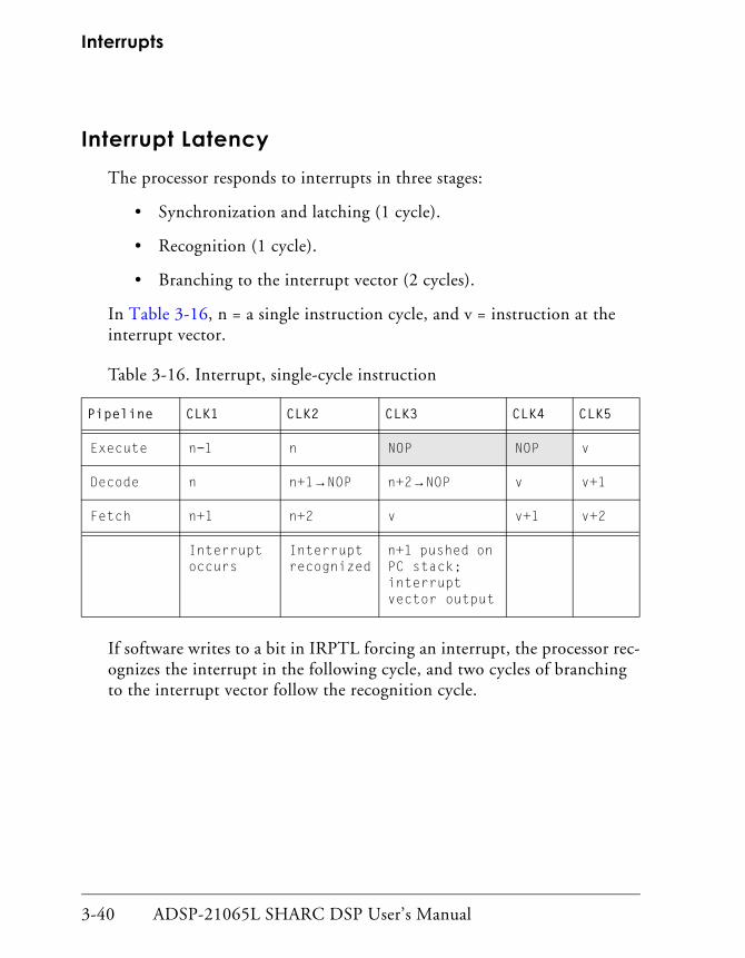
Interrupts
3-40 ADSP-21065L SHARC DSP User’s Manual
Interrupt LatencyThe processor responds to interrupts in three stages:
• Synchronization and latching (1 cycle).
• Recognition (1 cycle).
• Branching to the interrupt vector (2 cycles).
In Table 3-16, n = a single instruction cycle, and v = instruction at the interrupt vector.
If software writes to a bit in IRPTL forcing an interrupt, the processor rec-ognizes the interrupt in the following cycle, and two cycles of branching to the interrupt vector follow the recognition cycle.
Table 3-16. Interrupt, single-cycle instruction
Pipeline CLK1 CLK2 CLK3 CLK4 CLK5
Execute n−1 n NOP NOP v
Decode n n+1→NOP n+2→NOP v v+1
Fetch n+1 n+2 v v+1 v+2
Interrupt occurs
Interrupt recognized
n+1 pushed on PC stack; interrupt vector output

ADSP-21065L SHARC DSP User’s Manual 3-41
Program Sequencing
In Table 3-17, n = an instruction coinciding with a cache miss of a data access of program memory, and v = instruction at the interrupt vector.
In Table 3-18, n = a delayed branch instruction, v = instruction at the interrupt vector, and j = instruction at the branch address.
Table 3-17. Interrupt, program memory data access with cache miss
Pipeline CLK1 CLK2 CLK3 CLK4 CLK5 CLK6
Execute n−1 n NOP NOP NOP v
Decode n n+1→NOP n+1→NOP n+2→NOP v v+1
Fetch n+1 — n+2 v v+1 v+2
Inter-rupt occurs
Inter-rupt rec-ognized, but not pro-cessed; program memory data access
Inter-rupt pro-cessed
n+1 pushed onto PC stack; inter-rupt vector output

Interrupts
3-42 ADSP-21065L SHARC DSP User’s Manual
For most interrupts, internal and external, the core executes only one instruction after the interrupt occurs (and before the two instructions abort), while the processor fetches and decodes the first instruction of the service routine. After an arithmetic exception, however, two cycles occur before the processor starts processing an interrupt because of the one-cycle delay between an arithmetic exception and the update of the STKY register.
Table 3-19 on page 3-43 lists and the standard latency associated with the IRQ2-0 interrupts and the multiprocessor vector interrupt.
Table 3-18. Interrupt, delayed branch
Pipeline CLK1
CLK2
CLK3
CLK|4
CLK5
CLK6
CLK7
Execute n−1 n n+1 n+2 NOP NOP v
Decode n n+1 n+2 j→NOP j+1→NOP v v+1
Fetch n+1 n+2 j j+1 v v+1 v+2
Inter-rupt occurs
Inter-rupt recog-nized, but not pro-cessed
For call, n+3 pushed on PC stack; inter-rupt pro-cessed
j pushed on PC stack; inter-rupt vector output

ADSP-21065L SHARC DSP User’s Manual 3-43
Program Sequencing
If nesting is enabled and a higher priority interrupt occurs immediately after a lower priority interrupt, the service routine of the higher priority interrupt is delayed one additional cycle. (See “Interrupt Nesting and IMASKP” on page 3-46.) This delay enables execution of the first instruc-tion of the lower priority interrupt routine before that routine is interrupted.
Certain processor operations that span more than one cycle hold off inter-rupt processing. If an interrupt occurs during one of these operations, the processor synchronizes and latches it, but delays processing it. The opera-tions that delay interrupt processing this way are:
• A branch (call, jump, or return) and the following cycle, whether it is an instruction (in a delayed branch) or a NOP (in a nondelayed branch)
• The first of the two cycles needed to perform a program memory data access and an instruction fetch (when an instruction cache miss occurs).
• The third-to-last iteration of a one-instruction loop.
• The last iteration of a one-instruction loop executed once or twice, or the last iteration of a two-instruction loop executed once and the following cycle (which is a NOP).
Table 3-19. Minimum latency of the IRQ2-0 and VIRPT interrupts
Interrupt Minimum Latency
IRQ2-0 3 cycles
VIRPT 6 cycles
Interrupts
3-44 ADSP-21065L SHARC DSP User’s Manual
• The first of the two cycles needed to fetch and decode the first instruction of an interrupt service routine.
• Wait states for external memory accesses.
• An external memory access when the processor does not have con-trol of the external bus (during a host bus grant or when the proces-sor is a bus slave in a multiprocessing system).
Interrupt Vector TableThe IRPTL and IMASK registers contain all processor interrupts. For a complete list and detailed information, see Appendix F, Interrupt Vector Addresses, in ADSP-21065L SHARC DSP Technical Reference.
Interrupt Latch Register (IRPTL)The interrupt latch (IRPTL) register is a 32-bit register that latches inter-rupts. It indicates all interrupts the processor is currently servicing and those that are pending. Because this register is readable and writable, soft-ware can set or clear any interrupt, except reset. Writing to the reset bit (bit 1) in IRPTL places the processor in an illegal state.
When an interrupt occurs, it sets the corresponding bit in IRPTL. During execution of the interrupt’s service routine, this bit remains cleared—the processor clears it during each cycle. This scheme prevents the processor from latching the same interrupt while it executes the interrupt’s service routine.
A special method, however, enables applications to reuse an interrupt while the processor is servicing it. The clear interrupt (CI) modifier of the JUMP instruction provides this capability. See “Clearing the Current Interrupt for Reuse” on page 3-49.
IRPTL is cleared by a processor reset. The bits in the IMASK register cor-respond exactly to those in IRPTL.

ADSP-21065L SHARC DSP User’s Manual 3-45
Program Sequencing
Interrupt PriorityThe interrupt bits in IRPTL are ordered by priority. The interrupt prior-ity ranks from 0 (highest) to 31 (lowest).
Interrupt priority determines which interrupt the processor services first when more than one occurs in the same cycle and which interrupts are nested when nesting is enabled (see “Interrupt Nesting and IMASKP” on page 3-46).
The arithmetic interrupts—fixed-point overflow and floating-point over-flow, underflow, and invalid operation—are determined from flags in the sticky status register (STKY). Reading these flags, the service routine for one of these interrupts determines which condition caused the interrupt. The service routine must clear the appropriate STKY bit, to prevent the interrupt from remaining active after the service routine has finished.
When enabled, both of the programmable timers generate interrupts according to the operation mode in which they are set. You use the INT_HIx bits in the MODE2 register to configure each timer to either bit 4, TMZHI, or to bit 23, TMZLI of the IRPTL register. You can mask both of these interrupts in the IMASK register. (For details on configuring and using the programmable timers, see Chapter 11, Programmable Tim-ers and I/O Ports.)
The programmable timer feature enables you to choose the priority of the timer interrupt. You can configure both timers to latch to the same loca-tion or each timer to latch to a separate location. But, only the timer interrupt on the TMZHI bit pushes the status stack.
When both timers latch to the same location, the processor logically ORs both inputs and latches the value in the appropriate bit in the IRPTL reg-ister. To determine its source and service the interrupt, you must check its CNT_EXPx or PULSE_CAPx status bit in the STKY register.
Interrupts
3-46 ADSP-21065L SHARC DSP User’s Manual
Interrupt Masking and ControlTo enable and disable all interrupts, except reset, you set the global inter-rupt enable bit, IRPTEN, bit 12 in the MODE1 register. The processor clears this bit at reset. You must set this bit to enable interrupts.
Interrupt Mask Register (IMASK)
You can mask all interrupts, except reset. Masked means disable. Since the processor still latches (in IRPTL) interrupts that are masked, it processes interrupts that later become unmasked.
The IMASK register controls interrupt masking. The bits in IMASK cor-respond exactly to the bits in the IRPTL register.
For example, bit 10 in IMASK masks or unmasks the same interrupt that bit 10 in IRPTL latches.
• If a bit in IMASK is set (1), its interrupt is unmasked (enabled).
• If the bit is cleared (0), the interrupt is masked (disabled).
After reset, all interrupts except for reset and the EP0I interrupt for exter-nal port DMA channel 8 (bit 16 of IMASK) are masked. The reset interrupt is always nonmaskable. The processor automatically unmasks the EP0I interrupt after reset if an EPROM or a host is booting the processor.
Interrupt Nesting and IMASKP
The processor supports nesting of one interrupt service routine inside another. That is, a higher priority interrupt can interrupt a service routine. The nesting mode bit (NESTM) in the MODE1 register controls this feature.

ADSP-21065L SHARC DSP User’s Manual 3-47
Program Sequencing
NESTM=0 Disable interrupt service routine nesting.
The processor services any interrupt that occurs, but only after the routine finishes.
NESTM=1 Enable interrupt service routine nesting.
Higher priority interrupts can interrupt if they are not masked, but lower or equal priority interrupts cannot inter-rupt.
Make sure to change the NESTM bit outside of an interrupt service rou-tine or during the reset service routine only. Otherwise, interrupt nesting may not work correctly.
If nesting is enabled and a higher priority interrupt occurs immediately after a lower priority interrupt, the service routine of the higher priority interrupt is delayed one cycle. This enables execution of the first instruc-tion of the lower priority interrupt routine before the routine is interrupted.
In nesting mode, the processor uses the interrupt mask pointer (IMASKP) to create a temporary interrupt mask for each level of interrupt nesting—the IMASK value is not affected. The bits in IMASKP correspond to the same bits in IRPTL and IMASK and in the same order of priority. When an interrupt occurs, it sets its corresponding bit in IMASKP. The proces-sor changes IMASKP each time a higher priority interrupt interrupts a lower priority service routine. So, the bit in IMASKP that has the highest priority always corresponds to the interrupt the processor is servicing.
To generate a new temporary interrupt mask when nesting is enabled, the Program Sequencer masks all interrupts of equal or lower priority to the highest priority bit set in IMASKP and keeps higher priority interrupts the same as in IMASK. When it executes a return from an interrupt ser-vice routine (RTI), the Program Sequencer clears the highest priority bit set in IMASKP and masks all interrupts of equal or lower priority to the new highest priority bit set in IMASKP.

Interrupts
3-48 ADSP-21065L SHARC DSP User’s Manual
If nesting is disabled, the Program Sequencer masks out all interrupts and does not use IMASKP, although it still updates IMASKP to create a tem-porary interrupt mask.
The Program Sequencer updates IRPTL, but the processor does not vector to an interrupt that occurs while the processor is executing the interrupt’s service routine. The processor waits until the RTI finishes before vector-ing to the service routine again.
Status Stack Save and RestoreFor low-overhead interrupt servicing, the processor automatically saves and restores the status and mode contexts of the interrupted program. The three external interrupts (IRQ2-0), the timer interrupt, and the VIRPT vector interrupt cause an automatic push of ASTAT and MODE1 onto the status stack, which is five levels deep. The return from interrupt instruction RTI (and the JUMP (CI) instruction automatically pops these registers from the status stack. (See “Clearing the Current Interrupt for Reuse” on page 3-49.)
Pushing ASTAT and MODE1 preserves the status and control bit set-tings, so if the service routine alters these bits, the return from interrupt, RTI, automatically restores the original settings.
Only IRQ2-0, timer, and VIRPT interrupts push the status stack. All other interrupts require an explicit save and restore of the appropriate registers to memory.
Pushes and pops of the status stack do not affect the FLAG3-0 bits in ASTAT. The values of these bits carry over from the main pro-gram to the service routine and from the service routine back to the main program.

ADSP-21065L SHARC DSP User’s Manual 3-49
Program Sequencing
The top of the status stack contains the current values of ASTAT and MODE1. Reading and writing these registers does not move the stack pointer. Explicit PUSH and POP instructions, however, do move the stack pointer.
Software InterruptsThe processor provides software interrupts that emulate interrupt behav-ior but are activated through software instead of hardware.
Setting one of bits 28-31 in IRPTL with either a BIT SET instruction or a write to IRPTL activates a software interrupt. The processor branches to the corresponding interrupt routine if that interrupt is unmasked and interrupts are enabled.
Clearing the Current Interrupt for ReuseNormally, the processor ignores and does not latch an interrupt that reoc-curs while its service routine is executing. When the interrupt initially occurs, it sets its corresponding bit in IRPTL. During execution of the ser-vice routine, this bit remains cleared—the processor clears the bit during each cycle, preventing the processor from latching the same interrupt while it is executing the interrupt’s service routine.
The clear interrupt (CI) modifier of the JUMP instruction, however, enables an application to reuse an interrupt while it is undergoing servic-ing. This capability is useful in systems that require fast interrupt response and low interrupt latency. Be sure to place the JUMP (CI) instruction within the interrupt service routine. JUMP (CI) clears the status of the current interrupt without leaving the interrupt service routine. This reduces the interrupt routine to a normal subroutine and enables the interrupt to occur again, as a result of a different event or task in the system.

Interrupts
3-50 ADSP-21065L SHARC DSP User’s Manual
To reduce an interrupt service routine to a normal subroutine, the JUMP (CI) instruction clears the appropriate bit in the interrupt latch register (IRPTL) and interrupt mask pointer (IMASKP) and pops the status stack. This prevents the processor from clearing the interrupt’s latch bit (in IRPTL) in every cycle automatically, so the interrupt can occur again.
When returning from such a subroutine, the application must use the (LR) modifier of the RTS instruction (in case the interrupt occurred dur-ing the last two instructions of a loop). For details, see “General Restrictions” on page 3-27.
The following example shows how to use the (CI) modifier to reduce an interrupt service routine to a subroutine:
instr1; interrupt entry from main programJUMP(PC,3)(DB,CI); clear interrupt statusinstr3;instr4;instr5;RTS (LR); use LR modifier w/return from subrtn
The JUMP(PC,3)(DB,CI) instruction continues linear execution flow only by jumping to the location PC + 3 (instr5), with the processor exe-cuting the two intervening instructions (instr3, instr4) because of the delayed branch (DB). This JUMP instruction is only an example—a JUMP (CI) can jump to any location.
External Interrupt Timing and SensitivityEach of the processor’s three external interrupts, IRQ2-0, can be either level- or edge-triggered.
The processor samples interrupts twice every CLKIN cycle. Level-sensitive interrupts are considered valid if sampled active (low). A level-sensitive interrupt must go inactive (high) before the processor returns from the interrupt service routine. If a level-sensitive interrupt is still active when the processor samples it, the processor treats it as a new request, repeating

ADSP-21065L SHARC DSP User’s Manual 3-51
Program Sequencing
the same interrupt routine without returning to the main program (assuming no higher priority interrupts are active).
Edge-triggered interrupt requests are considered valid if sampled high in one cycle and low in the next. The interrupt can stay active indefinitely. To request another interrupt, the signal must go high, then low again.
Since they never a need to negate the request, edge-triggered interrupts require less external hardware than level-sensitive requests. However, mul-tiple interrupting devices can share a single level-sensitive request line on a wired-OR basis, which provides for easily expanded systems.
A bit for each interrupt in the MODE2 register indicates the sensitivity mode of each interrupt.
The processor accepts interrupts that are asynchronous to its clock; that is, an interrupt signal may change at any time. An asynchronous interrupt must be held low at least one CLKIN cycle to guarantee its sampling. Syn-chronous interrupts need only meet the setup and hold time requirements relative to the rising edge of CLKIN, as specified in the processor’s data sheet.
Asynchronous External Interrupts
Vector interrupts are used for interprocessor commands in multiprocessor systems. When an external processor, either another ADSP-21065L or a host, writes an address to the VIRPT register, it causes a vector interrupt.
Table 3-20. MODE2 interrupt mode bits
Bit Name Definition
0 IRQ0E 1 = edge-sensitive; 0 = level-sensitive
1 IRQ1E 1 = edge-sensitive; 0 = level-sensitive
2 IRQ2E 1 = edge-sensitive; 0 = level-sensitive

Interrupts
3-52 ADSP-21065L SHARC DSP User’s Manual
Multiprocessor Vector Interrupts (VIRPT)
When it services the vector interrupt, the processor automatically pushes the status stack and begins executing the service routine located at the address specified in VIRPT. The lower twenty-four bits of VIRPT contain the address, and applications can use the upper eight bits as data for the interrupt service routine. At reset, the processor initializes VIRPT to the standard address in the its interrupt vector table.
The minimum latency for vector interrupts is six cycles, five of which are NOPs. When the RTI (return from interrupt) instruction is reached in the service routine, the processor automatically pops the status stack.
The VIPD bit in SYSTAT reflects the status of the VIRPT register. If VIRPT is written while a previous vector interrupt is pending, the new vector address replaces the pending one. If VIRPT is written while a previ-ous vector interrupt is undergoing servicing, the processor ignores the new vector address, so no new interrupt is triggered. If the processor writes to its own VIRPT register, the write is ignored.
To use the processor’s vector interrupt feature, external processors per-form these actions:
1. Poll the VIRPT register until it reads a certain token value (0).
2. Write the vector interrupt service routine address to VIRPT.
When the service routine has finished, it writes the token back to VIRPT to indicate that it is done and that the processor can ini-tiate another vector interrupt.

ADSP-21065L SHARC DSP User’s Manual 3-53
Program Sequencing
Programmable TimersThe processor includes two programmable timers that your application can configure and use in either timer counter mode or in pulse counter/capture mode.
Each timer has one input/output pin—PWM_EVENTx. In timer counter mode (PMWOUT), this pin functions as an output pin, and in pulse counter/capture mode (WIDTH_CNT), this pin functions as an input pin.
Each timer has three registers—TPERIODx, TPWIDTHx, and TCOUNTx—that support timer functions. All timer registers are thirty-two bits wide, and the counters (TCOUNTx) use the system clock
(2x CLKIN), which evaluates to a maximum period of 71.5 sec ((232 -1)× 16.67ns system clock cycles) for the timer count.
For more details, see Chapter 11, Programmable Timers and I/O Ports.
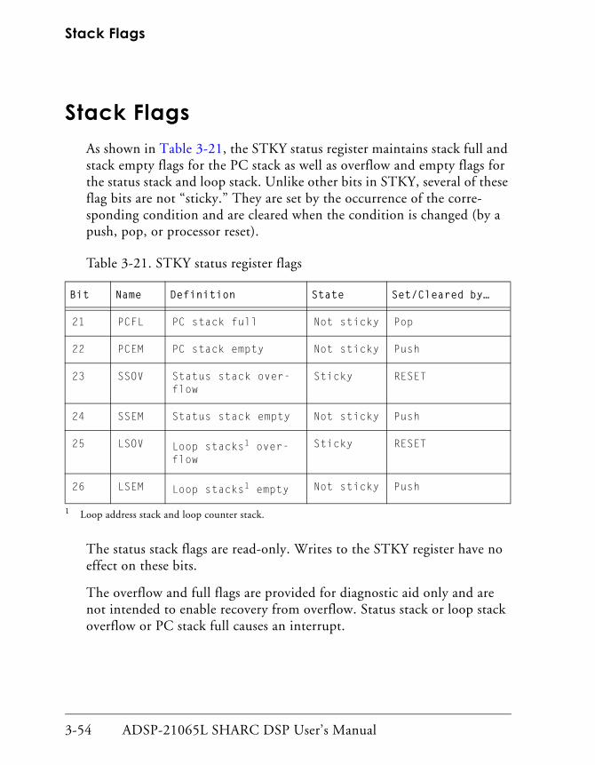
Stack Flags
3-54 ADSP-21065L SHARC DSP User’s Manual
Stack FlagsAs shown in Table 3-21, the STKY status register maintains stack full and stack empty flags for the PC stack as well as overflow and empty flags for the status stack and loop stack. Unlike other bits in STKY, several of these flag bits are not “sticky.” They are set by the occurrence of the corre-sponding condition and are cleared when the condition is changed (by a push, pop, or processor reset).
The status stack flags are read-only. Writes to the STKY register have no effect on these bits.
The overflow and full flags are provided for diagnostic aid only and are not intended to enable recovery from overflow. Status stack or loop stack overflow or PC stack full causes an interrupt.
Table 3-21. STKY status register flags
Bit Name Definition State Set/Cleared by…
21 PCFL PC stack full Not sticky Pop
22 PCEM PC stack empty Not sticky Push
23 SSOV Status stack over-flow
Sticky RESET
24 SSEM Status stack empty Not sticky Push
25 LSOV Loop stacks1 over-flow
1 Loop address stack and loop counter stack.
Sticky RESET
26 LSEM Loop stacks1 empty Not sticky Push

ADSP-21065L SHARC DSP User’s Manual 3-55
Program Sequencing
The empty flags facilitate stack saves to memory. You monitor the empty flag when saving a stack to memory to know when all values have been transferred. The empty flags do not cause interrupts because an empty stack is an acceptable condition.

Idle and Idle16
3-56 ADSP-21065L SHARC DSP User’s Manual
Idle and Idle16IDLE and IDLE16 are special instructions that halt the processor’s core in a low-power state until an external interrupt (IRQ2-0), timer interrupt, DMA interrupt, or VIRPT vector interrupt occurs.
When it executes an IDLE instruction, the processor fetches one more instruction at the current fetch address before suspending operation. The IDLE instruction does not affect the processor’s I/O processor, so any DMA transfers to or from internal memory continue uninterrupted.
Both the processor’s internal clock and the timer (if enabled) continue to run during IDLE. When an external interrupt (IRQ2-0), timer interrupt, DMA interrupt, or VIRPT vector interrupt occurs, the processor responds normally. After two cycles incurred in fetching and decoding the first instruction of the interrupt service routine, the processor continues exe-cuting instructions normally.
The IDLE16 instruction is a lower power version of the IDLE instruction. It executes a NOP and puts the processor in a low power state. Like the IDLE instruction, IDLE16 halts the processor, but the internal clock con-tinues to run at 1/16th the rate of CLKIN.
The processor remains in the low power state until an interrupt occurs.
To exit IDLE16, your application software can:
• Assert the external IRQx pin.
• Generate a timer interrupt.
After returning from the interrupt, execution continues at the instruction following the IDLE16 instruction.
While the processor is in IDLE16 mode, do not perform DMA transfers, SPORT transfers, or host transfers.
ADSP-21065L SHARC DSP User’s Manual 3-57
Program Sequencing
During IDLE16, the processor does not support:
• Host accesses
Make sure your application software does not assert HBR.
• Multiprocessor bus arbitration (synchronous accesses)
• External port DMA
• SDRAM accesses
• Serial port transfers

Instruction Cache
3-58 ADSP-21065L SHARC DSP User’s Manual
Instruction CacheThe processor’s on-chip instruction cache is a two-way, set-associative cache with entries for thirty-two instructions. This cache operates trans-parently to the programmer.
The processor caches only instructions that conflict with program memory data accesses (over the PMD bus with DAG2 generating the address on the PMA bus). This feature increases the efficiency of the cache consider-ably, surpassing performance of a cache that loads every instruction since, typically, only a few instructions must access data from a block of program memory.
Because of the three-stage instruction pipeline, if the instruction at address n requires a data access of program memory, it creates a conflict with the instruction fetch at address n+2, assuming sequential execution. The processor stores the fetched instruction (n+2) in the instruction cache, not the instruction that requires the data access of program memory.
If the instruction the processor needs is in the cache, a cache hit occurs—the cache provides the instruction while the processor performs a data access of program memory.
If the instruction the processor needs is not in the cache, a cache miss occurs, and the instruction fetch (from memory) takes place in the cycle following the data access of program memory and incurs one cycle of over-head. The Program Sequencer loads this instruction into the cache if the cache is enabled and not frozen, so the instruction (requiring program memory data) is available the next time the processor executes it.
Cache ArchitectureFigure 3-4 on page 3-59 shows a block diagram of the instruction cache. The cache contains thirty-two entries. An entry consists of a register pair

ADSP-21065L SHARC DSP User’s Manual 3-59
Program Sequencing
that contains an instruction and its address. Each entry has a valid bit, which is set if the entry contains a valid instruction.
The entries are divided into sixteen sets (numbered 15-0) of two entries each, entry 0 and entry 1. Each set has an LRU (Least Recently Used) bit whose value indicates which of the two entries contains the least recently used instruction (1=entry 1, 0=entry 0).
Each possible instruction address is mapped to a set in the cache by its four LSBs. When the processor needs to fetch an instruction from the cache, it uses the four address LSBs as an index to a particular set. Within that set, it checks the addresses of the two entries to see whether either contains the needed instruction. A cache hit occurs if the instruction is found, and the LRU bit is updated, if necessary, to indicate the entry that did not contain the needed instruction.
Figure 3-4. Instruction Cache architecture
A cache miss occurs if neither entry in the set contains the needed instruc-tion. If so, the processor loads a new instruction and its address into the least recently used entry of the set that matches the four LSBs of the address. It toggles the LRU bit to indicate that the other entry in the set is now the least recently used entry.
Set 0
Set 1
Set 2
Set 13
Set 14
Set 15
Instruction AddressLRUBit
ValidBit

Instruction Cache
3-60 ADSP-21065L SHARC DSP User’s Manual
Because the processor uses the four address LSBs of instructions to map them to sets, it doesn’t need to store these bits in the cache. The set in which the instruction has been stored implies the four address LSBs. A cache entry actually stores only bits 23:4.
Cache EfficiencyUsually, cache operation and its efficiency is not a concern. However, some situations can degrade cache efficiency, but your application can eas-ily remedy them.
When a cache miss occurs, the Program Sequencer loads the needed instruction into the cache, so if the same instruction is needed again, it is already there (causing a cache hit). However, if another instruction whose address is mapped to the same set displaces this instruction, a cache miss occurs. The LRU bits reduce cache misses since it takes fetches of at least two other instructions mapped to the same set to displace an instruction. If the processor repeatedly needs all three instructions mapped to the same set, cache efficiency (hit rate) can fall to zero (0). To avoid this, move one or more of the instructions to a new address, one that is mapped to a dif-ferent set.
Listing 3-1 is an example of cache-inefficient code:
Listing 3-1. Cache-inefficient code example
Address0x0100 lcntr=1024, do tight until lce;0x0101 r0=dm(i0,m0), pm(i8,m8)=f3;0x0102 r1=r0-r15;0x0103 if eq call (sub);0x0104 f2=float r1;0x0105 f3=f2*f2;0x0106 tight: f3=f3+f4;0x0107 pm(i8,m8)=f3;

ADSP-21065L SHARC DSP User’s Manual 3-61
Program Sequencing
•••0x0200 sub: r1=R13;0x0201 r14=pm(i9,m9);•••0x0211 pm(i9,m9)=r12;•••0x021F rts;
The data access of program memory at address 0x101 in the tight loop causes the Program Sequencer to cache the instruction at 0x103 (in set 3).
Each time the application calls the subroutine sub, the program memory data accesses at 0x201 and 0x211 load the instructions at 0x203 and 0x213 into set 3 and displace this instruction. If the subroutine is called only rarely during the loop execution, the impact will be minimal. If the subroutine is called frequently, the effect will be noticeable.
If the execution of the loop is time-critical, moving the subroutine up one location (starting at 0x201) is advisable, so the two cached instructions end up in set 4 instead of in set 3.
Cache Disable and Cache FreezeFreezing the cache prevents any changes to its contents—a cache miss does not result in storage of a new instruction in the cache.
Disabling the cache stops its operation completely. The access delays all instruction fetches that conflict with data accesses of program memory.

Instruction Cache
3-62 ADSP-21065L SHARC DSP User’s Manual
The CADIS (cache enable/disable) and CAFRZ (cache freeze) bits in the MODE2 register select the functions shown in Table 3-22.
After reset, the cache is cleared, so it contains no instructions, but is unfrozen and enabled.
Do not place an instruction that contains a data access of program mem-ory directly after a cache enable or a cache disable instruction—the processor must wait at least one cycle before executing the PM data access. You can insert a NOP instruction to provide this delay.
Bit 4 (CADIS) directs the sequencer to disable the cache (if 1) or enable the cache (if 0). Disabling the cache does not mark the current content of the cache as invalid. If the cache is enabled again, the existing content is used again. To clear the cache, use the FLUSH CACHE instruction.
If you are using self-modifying code (for example, software loader kernel) or software overlays, execute a FLUSH CACHE instruction followed by a NOP before executing the new code. Otherwise, old con-tent from the cache could still be used, even though the code has changed.
Table 3-22. MODE2 CADIS and CAFRZ bits
Bit Name Function
4 CADIS Cache Disable
19 CAFRZ Cache Freeze
ADSP-21065L SHARC DSP User’s Manual 4-1
4 DATA ADDRESSINGFigure 4-0.
Table 4-0.
Listing 4-0.
Maintaining pointers into memory, the processor’s two data address gen-erators (DAGs) simplify the task of organizing data. The DAGs enable the processor to address memory indirectly; that is, an instruction specifies a DAG register that contains the address of a value instead of the value.
Data address generator 1 (DAG1) generates 32-bit addresses on the DM Address Bus. Data address generator 2 (DAG2) generates 24-bit addresses on the PM Address Bus. Figure 4-1 on page 4-3 shows the basic architec-ture of both DAGs. For details, see “Generating Addresses for the PM and DM Buses” on page 5-11.
The DAGs provide hardware support for some functions commonly used in digital signal processing algorithms. Both DAGs support circular data buffers, which require software to advance a pointer repetitively through a range of memory locations. Both DAGs can also perform a bit-reversing operation, which outputs the bits of an address in reversed order.

DAG Registers
4-2 ADSP-21065L SHARC DSP User’s Manual
DAG RegistersEach DAG has four types of registers: Index (I), Modify (M), Base (B), and Length (L).
An I register acts as a pointer to memory, and an M register contains the value to increment the pointer. To vary the increment as needed, you modify an I register with different M values.
B and L registers work with circular data buffers only. These buffers oper-ate in pairs: B0 with L0, B4 with L4, B12 with L12, and so on. The B register holds the base address (first address) of a circular buffer. The cor-responding L register contains the number of locations in the circular buffer, defining its length.
Each DAG contains eight of each register type, as shown in Table 4-1.
Table 4-1. DAG registers
DAG1 (32-bit) DAG2 (24-bit)
B0-B7 B8-B15
I0-I7 I8-I15
M0-M7 M8-M15
L0-L7 L8-L15

ADSP-21065L SHARC DSP User’s Manual 4-3
Data Addressing
Figure 4-1. Architecture of the data address generators (DAGs)
Alternate DAG RegistersTo implement context switching, each DAG register has an alternate reg-ister. Figure 4-2 on page 4-4 shows how each DAG is organized into upper and lower halves for activating its alternate registers.
.
!
/0
.
/0
/0
1
%
/0
1
.2 3%456 /3%457
3- 5
+%.3%45
%.3%45
-
.23- 5
!
%4&8
%4&8) )
"

DAG Registers
4-4 ADSP-21065L SHARC DSP User’s Manual
Figure 4-2. Alternate DAG registers
The upper half of DAG1 contains I, M, B and L registers 4 through 7, and the lower half contains I, M, B and L registers 0 through 3.
Likewise, the upper half of DAG2 contains I, M, B and L registers 12 through 15, and the lower half contains I, M, B and L registers 8 through 11.
!
!
!
!
.
.
.
.
)
(
)
(
!)
!(
!
!
.)
.(
.
.
/
/
!/
!
!
!
./
.
.
.
)
(
)
(
!
!
!)
!(
.
.
.)
.(
,#.
#!
#9
#!
#9
%43 "75
%43+ ""75

ADSP-21065L SHARC DSP User’s Manual 4-5
Data Addressing
Table 4-2 shows the control bits in the MODE1 register that determine, for each half, whether the DAG’s primary or alternate registers are active.
This grouping of alternate registers enables you to pass pointers between contexts in each DAG.
Table 4-2. MODE1 DAG control bits for
Bit Name Definition
3 SRD1H DAG1 alternate register select (7-4)
4 SRD1L DAG1 alternate register select (3-0)
5 SRD2H DAG2 alternate register select (15-12)
6 SRD2L DAG2 alternate register select (11-8)
0 = primary registers; 1 = alternate registers

DAG Operation
4-6 ADSP-21065L SHARC DSP User’s Manual
DAG OperationDAG operations include:
• Address output with premodify or postmodify.
• Modulo addressing (for circular buffers).
• Bit-reversed addressing.
The DAGs right-shift short word addresses (16-bit data) by one bit before outputting them on the DM Address Bus. This enables internal memory to use the address directly. (For details, see “Using 16-Bit Short Word Accesses” on page 5-41.)
Address Output and ModificationThe processor can generate addresses in one of two ways:
• Premodify operation
The processor adds an offset (modifier), either an M register or an immediate value, to an I register and outputs the resulting address.
This operation does not update the value of the I register.
Neither the L register nor modulo logic affect a premodified address. Premodify addressing is always linear, never circular.
Restrictions on the use of premodify addressing operations may apply to some older silicon revisions. For details, see “Memory Organization” on page 5-16.
• Postmodify operation
The processor outputs the I register value as is and adds an M regis-ter or immediate value to form a new I register value.

ADSP-21065L SHARC DSP User’s Manual 4-7
Data Addressing
The width of an immediate modifier depends on the instruction. It can be as large as the width of the I register.
Figure 4-3 shows a comparison of the pre- and postmodify operations.
Figure 4-3. Comparison of premodify and postmodify operations
DAG Modify Instructions
In the processor’s assembly language, the positions of the index and modi-fier (M register or immediate value) in the instruction distinguishes the premodify and postmodify operations.
The I register coming before the modifier identifies the postmodify opera-tion. Conversely, the modifier coming before the I register identifies the premodify with no update operation. For example, the following instruc-tion accesses the program memory location with an address equal to the
If you use postmodify addressing without implementing a circu-lar buffer, make sure you set the corresponding L register to 0.
Uninitialized L registers cause unpredictable postmodify behav-ior.
'
- '
:-
'
'
:-
+, ;<
-
+# ;<
-
+3 0=05
3 0=05
+30= 05
30= 05

DAG Operation
4-8 ADSP-21065L SHARC DSP User’s Manual
value stored in I15, and the processor writes back the value I15 + M12 to the I15 register:
R6 = PM(I15,M12); Indirect addressing with postmodify
If the order in which the I and M registers appear in the instruction is reversed, the instruction accesses the location in program memory with an address equal to I15 + M12, but without changing the value of I15:
R6 = PM(M12,I15); Indirect addressing with premodify
Any M register can modify any I register within the same DAG (DAG1 or DAG2). So,
DM(M0,I2) = R0; valid instructionDM(M0,I14) = R0; invalid instruction
Immediate Modifiers
The magnitude of an immediate value that can modify an I register depends on the instruction type and whether the I register is in DAG1 or in DAG2.
DAG1 modify values can be up to 32-bits wide. DAG2 modify values can be up to 24-bits wide. Some instructions with parallel operations support modify values up to 6-bits wide only. For example:
• 32-bit modifier
R1=DM(0x00400000,I1); DM address = I1 + 0x0040 0000
• 6-bit modifier:
F6=F1+F2,PM(I8,0x0B)=ASTAT; PM address = I8, I8 = I8 + 0x0B

ADSP-21065L SHARC DSP User’s Manual 4-9
Data Addressing
Circular Buffer AddressingThe DAGs provide addressing of locations within a circular data buffer.
A circular buffer consists of a set of memory locations that stores data and an index pointer that steps through the buffer. For each step, the processor postmodifies and updates the buffer’s I register by adding the value (posi-tive or negative) specified in the M register to the value in the I register.
If the modified address pointer (M) falls outside the circular buffer, the processor either subtracts or adds, accordingly, the length of the buffer to the value to wrap the index pointer back to the start of the buffer (see Figure 4-4). The value of the base address of a circular buffer carries no restrictions.
Figure 4-4. Circular data buffers
For circular buffer addressing, you must use M registers to postmodify I registers, not to premodify them.
)
(
/
)
(
/
)
(
)
(
/
/
)
(
/
#> - :
#>- ?>- :
!@8
. 8
8)

DAG Operation
4-10 ADSP-21065L SHARC DSP User’s Manual
For example:
F1=DM(I0,M0);Use a postmodify operation tomodify circular buffers, not a premodifyoperation.
Circular Buffer Operation
To set up a circular buffer in assembly language, initialize an L register with a positive, nonzero value and load the corresponding B register with the base (starting) address of the buffer. The processor automatically loads the corresponding I register with this same starting address.
On the first postmodify access using the I register, the DAG outputs the I register value on the address bus and then modifies it by adding to it the value specified in the M register or an immediate value.
If the modified value is within the buffer’s range, the DAG writes it back to the I register. If the value is outside the buffer’s range, the DAG sub-tracts (or adds if the modify value is negative) the L register value to the modified value before writing the modified value back to the I register.
• If M is positive
Inew=Iold + M If Iold+M < Buffer base + length(end of buffer)
Inew=Iold + M–L If Iold+M ≥ Buffer base + length (end of buffer)
• If M is negative
Inew=Iold + M If Iold+M ≥ Buffer base(start of buffer)
Inew=Iold + M + L If Iold+M < Buffer base(start of buffer)
ADSP-21065L SHARC DSP User’s Manual 4-11
Data Addressing
Circular Buffer Registers
A circular buffer uses all four types of DAG registers:
• The I register contains the value the processor outputs on the address bus.
• The M register contains the postmodify value (positive or negative) that the processor adds to the I register at the end of each memory access.
You can use any M register providing it is located in the same DAG as the I register. And you can use noncorresponding M and I register combinations; for example, registers M2 and I4.
You can use an immediate value or an M register value for the mod-ifier. The magnitude of the modify value, whether from an M reg-ister or an immediate value, must be less than the length (L register) of the circular buffer.
• The L register sets the size of the circular buffer, defining the address range that the I register steps through.
The value of the L register must be positive and cannot have a value
greater than 231−1 (for L0 through L7) or 223 −1 (for L8 through L15). A value of 0 in an L register disables the circular buffer.
• After each access, the processor compares the modified I value to the B register value, or the sum of the B and L registers.
When the processor loads the B register, it also loads the corre-sponding I register with the same value. When it loads the I register,
If you use postmodify addressing without implementing a circular buffer, make sure you set the corresponding L register to 0.

DAG Operation
4-12 ADSP-21065L SHARC DSP User’s Manual
it does not change the value in the B register. You can read the B and I registers independently.
Circular Buffer Overflow Interrupts
Circular buffer overflow interrupts are useful in implementing, for exam-ple, a ping-pong routine that swaps I/O buffer pointers.
One set of registers in each DAG can generate an interrupt when a circular buffer overflows (address wraparound occurs). In DAG1, the registers are B7, I7, and L7, and in DAG2, they are B15, I15, and L15.
A circular buffer addressing operation that uses these registers and causes the processor to increment or decrement the address in the I register past the end or start of the circular buffer generates an interrupt. Which inter-rupt is generated depends on the register set the operation used, as shown in Table 4-3.
Specifically, an instruction generates an interrupt during its address post-modify when:
(for M<0) I + M < B(for M≥0) I + M ≥ B + L
Table 4-3. Circular buffer overflow interrupts
Interrupt Use DAG… Vector Addr SymbolicName1
1 These symbols are defined in the #include file def21065L.h. For details, see Appendix E, Control and Status Registers, in ADSP-21065L SHARC DSP Technical Reference.
DAG1 circular buffer 7 overflow
B7, I7, L7 0x54 CB7I
DAG2 circular buffer 15 overflow
B15, I15, L15 0x58 CB15I
ADSP-21065L SHARC DSP User’s Manual 4-13
Data Addressing
To mask these interrupts, clear the appropriate bit in the IMASK register.
In certain situations, you may want to use I7 or I15 without circular buff-ering, but with the circular buffer overflow interrupts unmasked. To disable generation of these interrupts, set the B7 and B15 registers in DAG1 and the L7 and L15 registers in DAG2 to values that ensure the conditions that generate interrupts never occur. For example, when access-ing the address range 0x1000 to 0x2000, set B=0x0000 and L=0xFFFF. (Setting the L register to zero (0) will not disable circular buffer interrupts.)
If you are using either of the circular buffer overflow interrupts, avoid using the corresponding I register(s) (I7 and I15) in the rest of your appli-cation software, or make sure your software sets the B and L registers accordingly to prevent spurious interrupt branching.
The STKY status register contains two bits that the processor sets when a circular buffer overflow occurs—bit 17 (DAG1 circular buffer 7 overflow) and bit 18 (DAG2 circular buffer 15 overflow). These bits are “sticky” and remain set until explicitly cleared.
Bit ReversalYou can bit-reverse memory addresses two ways:
• Enabling bit-reverse mode on DAG1 or DAG2 and using a specific I register (I0 or I8).
• Using the explicit bit-reverse instruction BITREV.
Using Bit-Reverse Mode
In bit reverse mode, DAG1 bit-reverses 32-bit address values output from I0, and DAG2 bit-reverses 24-bit address values output from I8.
The processor bit reverses the address values from the I0 and I8 registers only.

DAG Operation
4-14 ADSP-21065L SHARC DSP User’s Manual
This mode affects both premodify and postmodify operations.
The BR0 and BR8 bits in the MODE1 register enable these modes.
Bit reversal occurs at the output of the DAG and does not affect the value in I0 or I8. In postmodify operations, the processor does not bit reverse the update value.
For example:
I0=0x80400000;R1=DM(I0,3); DM address=0x201, I0=0x80400003
Using the Bit Reverse Instruction
The BITREV instruction modifies and bit reverses addresses in any DAG index register (I0-I15), without actually accessing memory. This instruc-tion operates independently of bit-reverse mode.
The BITREV instruction:
• Adds a 32-bit immediate value to a DAG1 index register. For a DAG2 index register, you can specify a zero immediate value only.
• Bit-reverses the result.
• Writes the result back to the same index register.
For example:
BITREV(I9,0); I9 = Bit-reverse of (I9+0)
Table 4-4. MODE1 bit reversal mode bits
Bit Name Description
0 BR8 Bit reverse mode for I8 (DAG2)
1 BR0 Bit reverse mode for I0 (DAG1)

ADSP-21065L SHARC DSP User’s Manual 4-15
Data Addressing
DAG Register TransfersDAG registers are part of the universal register set. You can write to them from memory, from another universal register, or from an immediate field in an instruction. Conversely, you can write DAG register contents to memory or to a universal register.
As shown in Figure 4-5, transfers between 32-bit DAG1 registers and the 40-bit Data Memory Data (DMD) bus are aligned to bits 39:8 of the DMD bus.
Figure 4-5. DAG register transfers
When the processor reads 24-bit DAG2 registers over the 40-bit DMD bus, it sign-extends M register values to 32 bits and zero-fills I, L, and B register values to 32 bits. The results are aligned to bits 39:8 of the DMD Bus.
When the processor writes the DAG2 registers from the DMD bus, it transfers bits 31:8 and ignores the rest.
/A /A
%43(2/5/?
/A
/A
%4325
%43(2/5
%4 =!=.:3(2/5
DAG Register Transfers
4-16 ADSP-21065L SHARC DSP User’s Manual
For certain instruction sequences that involve transfers to and from DAG registers, the processor inserts a NOP cycle automatically.
Certain other sequences, which the assembler does not support, cause incorrect results:
• Instructions that generate an extra NOP cycle
The processor automatically inserts a NOP cycle between two con-secutive instructions if the first instruction loads a DAG register and the second instruction uses any register in the same DAG for data addressing, modify instructions, or indirect jumps.
The processor inserts the NOP instruction to delay the second oper-ation since both operations need the same bus in the same cycle.
For example:
L2=8;DM(I0,M1)=R1;
Because L2 is in the same DAG as I0 (and M1), the processor inserts an extra cycle after the write to L2.
• Illegal instructions that generate incorrect results
You can execute the following types of instructions on the proces-sor, but they generate incorrect results and are unsupported:
• An instruction that uses indirect addressing from a DAG to store the same DAG register in memory, with or without updating the index register.
This instruction writes the wrong data to memory or updates the wrong index register.
For example: DM(M2,I1)=I0;orDM(I1,M2)=I0;
ADSP-21065L SHARC DSP User’s Manual 4-17
Data Addressing
• An instruction that uses indirect addressing from a DAG to load the same DAG register from memory and updates the index reg-ister.
This instruction either loads the DAG register or updates the index register, but not both.
For example: L2=DM(I1,M0);

DAG Register Transfers
4-18 ADSP-21065L SHARC DSP User’s Manual
ADSP-21065L SHARC DSP User’s Manual 5-1
5 MEMORYFigure 5-0.
Table 5-0.
Listing 5-0.
The processor’s dual-ported SRAM provides 544K bits of on-chip storage for program instructions and data.
The processor’s internal bus architecture provides a total memory band-width of 900M bytes/sec., enabling the core to access 660M bytes/sec. and the I/O processor to access 264M bytes/sec. of memory
The processor’s flexible memory structure enables:
• The processor’s core and I/O processor or DMA controller to inde-pendently access memory in the same cycle.
• The processor’s core to access both memory blocks in parallel using its PM and DM buses.
• Applications to configure memory to store 16-, 32-, 40-, or 48-bit words or combinations of these.
The processor uses 32-bit memory words for single-precision IEEE floating-point data and 48-bit words for instructions. It supports 16-bit short word format for integer or fractional data values.

5-2 ADSP-21065L SHARC DSP User’s Manual
Figure 5-1. ADSP-21065L block diagram
The following terms are used throughout this chapter:
DAGs Data Address Generators.
Generate indirect addresses for data reads and writes over the PM and DM buses. The DAGs generate addresses simultaneously for dual operand reads and writes if the instruction is available in the Instruction Cache. See also, Instruction Cache.
DAG1 generates 32-bit addresses for data transfers over the DM bus. DAG2 generates 24-bit addresses for data transfers over the PM bus.
For more information see, Chapter 4, Data Addressing.
DATAADDR DATAADDR
BLO
CK
1
TWO INDEPENDENT
DUAL-PORTED BLOCKS
PROCESSORPORT
I/OPORT
ADDR DATA DATAADDR
BLO
CK
0
IOPRegisters
DMAController
ProgramSequencer
Instructioncache
32x48b
24
32
48
40
PM Address Bus
DM Data Bus
PM Data Bus
DM Address Bus
IOA17
IOD48
I/O Processor
Dual-Ported SRAM
SDRAMInterface
MultiprocessorInterface
DATABus Mux
PMD
DMD
EPD
ADDRBus Mux
PMA
DMA
EPA
IOD
EP
D
DM
D
PM
D
EP
A
IOA
External PortDAG18x4x32
DAG28x4x24
BusConnect
(PX)
DSP Core
DataRegister
File
ADSP-21065L SHARC DSP User’s Manual 5-3
Memory
DM busData Memory bus.
Consists of the 32-bit Data Memory Address (DMA) bus and the 40-bit Data Memory Data (DMD) bus.
Controlled by the processor’s core, the DM bus provides a connec-tion between SRAM, core (DAGs, PX bus connect, Register File, Programs Sequencer, and Instruction Cache), I/O processor’s IOP registers, and the external port.
Used to transfer data between registers and between registers and external memory. Transfers are done within one clock cycle.
See also, PM bus.
External memory spaceMemory map area that corresponds to external memory.
See also, Internal memory space, Multiprocessor memory space.
External port Provides addressing of up to 64M words of additional, off-chip memory and access to other peripherals, a host processor, and the IOP registers of the other ADSP-21065L in a multiprocessing system.
Instruction CacheOne of two sources (PM bus and Instruction Cache) for tempo-rarily storing the next instruction that the processor needs to fetch.
When the Instruction Cache provides instructions, it eliminates PM bus conflicts that can occur when the core uses the PM bus to execute a dual-data access. This way, data accesses over the PM bus incur no extra cycles.
5-4 ADSP-21065L SHARC DSP User’s Manual
The Instruction Cache stores only those instructions that conflict with data accesses over the PM bus.
Internal memory space Memory map area that corresponds to the processor’s internal memory.
See also, External memory space, Multiprocessor memory space.
I/O bus The input/output bus connecting SRAM with the I/O processor.
Controlled by the I/O processor, the I/O bus enables concurrent data transfers between either memory block and the processor’s communications ports (the external port and serial ports).
See also, Memory blocks, External port.
IOP registersThe I/O processor’s I/O registers that provide the interface for:
• Accesses into the processor’s internal memory made by a host, another ADSP-21065L in a multiprocessor system, or any other peripheral device.
• Accesses into the processor’s configuration and status infor-mation made by the processor’s DMA controller.
For more information, see Chapter 8, Host Interface.
Memory blocksThe two partitions of the processor’s on-chip SRAM.
Block 0’s 288K bits of 6K x 48 memory is organized into nine col-umns of 16 x 2k. Block 1’s 256K bits of 8K x 32 memory is organized into eight columns of 16 x 2k.
ADSP-21065L SHARC DSP User’s Manual 5-5
Memory
The processor’s core and the I/O processor can access each block in every cycle. When both access the same block, the accesses incur no extra cycles.
Multiprocessor memory space Memory map area that corresponds to the IOP registers of another ADSP-21065L in a multiprocessor system.
See also, External memory space, Internal memory space.
PM bus Program Memory bus.
Consists of the Program Memory Address (PMA) bus, a 24-bit transmission path, and the Program Memory Data (PMD) bus, a 48-bit transmission path.
Controlled by the processor’s core, the PM bus provides a connec-tion between SRAM, core (DAGs, PX bus connect, Register File, Program Sequencer, and Instruction Cache), I/O processor’s IOP registers, and the external port.
Used to transfer instructions and data.
See also, DM bus.
Program SequencerGenerates 24-bit PM bus addresses for instruction fetches from memory.
See Chapter 3, Program Sequencing.
PX bus connectionProvides the internal exchange mechanism for passing data between the 48-bit PM bus and the 40-bit DM bus or the 40-bit Register File.

5-6 ADSP-21065L SHARC DSP User’s Manual
Consists of two subregisters, PX1 and PX2, which the processor’s core can access as one 48-bit register or as two separate registers, one 16-bit register (PX1) and one 32-bit register (PX2).
Register FileA set of 40-bit, universal registers located in the processor’s core in which the processor stores data to feed to or retrieve from the com-putation units.
See Chapter 2, Computation Units.
SDRAM interfacePart of the external port, the SDRAM interface enables the proces-sor to transfer data to and from off-chip synchronous DRAM at 2x CLKIN.
See Chapter 10, SDRAM Interface.

ADSP-21065L SHARC DSP User’s Manual 5-7
Memory
Transferring Data In and Out of MemoryThe processor has three internal buses connected to its dual-ported mem-ory—the PM bus, the DM bus, and the I/O bus. The PM and the DM buses connect to the memory’s processor port, and the I/O bus connects to the memory’s I/O port as shown in Figure 5-2.
Figure 5-2. Bus connections to on-chip SRAM memory
The processor’s core controls the PM and DM buses, and the I/O proces-sor controls the I/O bus. The I/O bus enables concurrent data transfers between either memory block and the processor’s communication ports (external and serial ports).
PROCESSORPORT
I/OPORT
ADDR
ADDR
ADDR
ADDR DATA
DATADATA
DATA
Two IndependentDual-Ported Blocks
Block 0 (6K x 48)
Blo
ck 1
(8K
x 3
2)
IOAIOD
PM One IOP AccessPer Cycle
(240 MBytes/s)Two Core AccessesPer Cycle
(660 MBytes/s)
DM DMPM

Transferring Data In and Out of Memory
5-8 ADSP-21065L SHARC DSP User’s Manual
Dual Data AccessesFigure 5-3 shows addresses that the processor generates for DM bus and PM bus accesses. (See page 5-20 for the processor’s address decoding table.) DAG1 generates DM bus addresses, and either the program sequencer or DAG2 generates PM bus addresses for instructions or data, respectively.
Figure 5-3. Memory address bits on the DM and PM buses
Although the processor has two separate internal buses, the Program Memory bus (PM) and the Data Memory bus (DM), memory itself remains undefined as either PM or DM, and applications can store data within program memory space. The processors’ modified Harvard archi-tecture enables applications to configure memory to store different combinations of code and data.
The independent PM and DM buses enable the core to simultaneously access instructions and data from the memory blocks. For single instruc-tions, however, core accesses of two words from the same memory block over the same bus incur an extra cycle. The core fetches instructions over the PM bus or from the instruction cache and data over both the DM bus using DAG1 and the PM bus using DAG2. Figure 5-2 on page 5-7 shows the memory bus connections on the processor.
31 30 29 28 27 26 25 24 23 22 21 20 19 18 17 16 15 14 13 12 11 10 9 8 7 6 5 4 3 2 1 0
% & Reserved
23 22 21 20 19 18 17 16 15 14 13 12 11 10 9 8 7 6 5 4 3 2 1 0
&
!'(
!'(
V = Virtual addressE = Memory addressS = IOP register addressM = IOP register spaceP = IOP register space address

ADSP-21065L SHARC DSP User’s Manual 5-9
Memory
Applications can configure the processor’s two memory blocks to store different combinations of 48-bit instruction words and 32-bit data words. However, configuring one block to contain a mix of instructions and PM bus data and the other block to contain DM bus data only achieves maxi-mum efficiency; that is, single-cycle execution of dual-data-access instructions.
This means for instructions that require two data accesses, the processor’s core uses the PM bus with DAG2 to access data from the mixed block and the DM bus with DAG1 to access data from the data-only block. The instruction for the core to fetch must be available in the instruction cache. As an alternative, the application can store one operand in external mem-ory space and the other in either block of internal memory space.
Typically, DSP applications, such as digital filters and FFTs, must access two data operands for some instructions. In a digital filter, for example, the filter can store coefficients in 32-bit words in the same memory block that contains the 48-bit instructions and store 32-bit data samples in the other block. This configuration facilitates single-cycle execution of dual-data-access instructions when the core uses DAG2 to access the filter coefficients over the PM bus, and the instruction is available in the instruction cache.
To ensure single-cycle, parallel accesses of two on-chip memory locations, the application must meet these conditions:
• The location of each address must be in a different internal memory block.
• DAG1 must generate one address, and DAG2 the other.
• The DAG1 address must point to a different memory block than the one from which the processor’s core is fetching the instructions.

Transferring Data In and Out of Memory
5-10 ADSP-21065L SHARC DSP User’s Manual
• The instruction takes the form:
compute, Rx=DM(I0 -I7,M0 -M7), Ry=PM(I8 -I15,M8 -M15);
Using the Instruction Cache to Access PM DataNormally, the processor fetches instructions over the 48-bit PM Data bus. Executing a dual-data-access instruction that requires reading or writing data over the PM bus, however, causes a bus conflict. By providing the instruction, the processor’s on-chip instruction cache can resolve this con-flict. The first time the instruction executes, the instruction cache stores it, making it available on the next fetch.
By providing the instruction, the cache enables the core to access data over the PM bus—the core fetches the instruction from the cache instead of from memory so that it can simultaneously transfer data over the PM bus. The instruction cache stores only those instructions whose fetches conflict with PM bus data accesses.
When the instruction to fetch is already cached—the instruction is exe-cuted within a loop—core data accesses over the PM bus incur no extra cycles. However, a cache miss always incurs an extra cycle when the core uses the PM bus to access both instruction and data, even if they are in different memory blocks.
In these instructions, reads and writes may be intermixed. A cache miss occurs whenever the fetched instruction is invalid during any DAG2 transfer. See “Instruction Cycle” on page 3-4.

ADSP-21065L SHARC DSP User’s Manual 5-11
Memory
Generating Addresses for the PM and DM BusesThe processor’s three internal buses—PM, DM, and I/O—connect to its dual-ported memory, with the PM and DM buses sharing one memory port, and the I/O bus connecting to the other.
The processor’s Program Sequencer and data address generators (DAGs) supply memory addresses. The Program Sequencer supplies 24-bit PM bus addresses for instruction fetches, and the DAGs supply addresses for data reads and writes. (See Figure 5-1 on page 5-2.)
Both data address generators enable indirect addressing of data. DAG1 supplies 32-bit addresses over the DM bus. DAG2 supplies 24-bit addresses for data accesses over the PM bus. If the instruction to fetch is available in the instruction cache, the DAGs can generate simultaneous addresses—over the PM bus and DM bus—for dual operand reads and writes.
The 48-bit PM Data bus transfers instructions (and data), and the 40-bit DM Data bus transfers data only. The PM Data bus is 48-bits wide to accommodate the 48-bit instruction width. When this bus transfers 32-bit data (floating- or fixed-point), the data is aligned to the upper 32 bits of the bus.
The 40-bit DM Data bus provides a path for transferring, in a single cycle, the contents of any register in the Register File to any other register or to any external memory location. Data addresses come from either an abso-lute value specified in the instruction (direct or immediate addressing) or from the output of a DAG (indirect addressing). Thirty-two-bit fixed-point and 32-bit single-precision floating-point data is aligned to the upper 32 bits of the DM Data bus.
The PX bus connect registers pass data between the 48-bit PM Data bus and the 40-bit DM Data bus or the 40-bit Register File. The PX registers contain hardware to handle the 8-bit difference in width.

Transferring Data In and Out of Memory
5-12 ADSP-21065L SHARC DSP User’s Manual
The three memory buses—PM, DM, and I/O—are multiplexed at the processor’s external port to create a single off-chip data bus (DATA31-0) and address bus (ADDR23-0).
Transferring Data Between the PM and DM BusesThe PX register provides an internal bus exchange path for transferring data between the 48-bit PM Data Bus and the 40-bit DM Data Bus. The 48-bit PX register consists of two subregisters, the PX1 and PX2 registers. PX1 is 16-bits wide and PX2 is 32-bits wide. Instructions can use the entire PX register or use PX1 and PX2 separately. Figure 5-4 shows the alignment of PX1 and PX2 within PX.
Figure 5-4. PX register
Instructions use the PX register(s) in universal register-to-register transfers or in memory-to-register (and vice versa) transfers. These transfers use either the PM Data Bus or the DM Data Bus. Instructions can read or write the PX register(s) from or to the PM Data Bus, the DM Data Bus, or the Register File.
Figure 5-5 shows the data alignment in PX register transfers. Transfers between PX2 and the PM Data Bus use the upper 32 bits of the PM Data Bus. On transfers from PX2, the sixteen LSBs of the PM Data Bus are filled with zeros. Transfers between PX1 and the PM Data Bus use the middle sixteen bits of the PM Data Bus. On transfers from PX1, bits PM15-0 and PM47-32 are filled with zeros (0).
47 15 0
PX2 PX1
PX Register

ADSP-21065L SHARC DSP User’s Manual 5-13
Memory
Figure 5-5. PX register transfers
16 zeros
PX2
47 15 0
PX1
16 zeros16 zeros
47 15 031
47 15 0
PX2 PX1
PX2
8 zeros
39 7 0
8 zeros
PX1
16 zeros
39 7 023
39 0
PX Register
Register File
47 7 0
PX Register
39 0
PX Register
To Internal Memory
47 7 0
8 zeros
PM Data Bus Transfers DM Data Bus or Register File Transfers
31
1516
0
47 0
To External Memory
PX1PX2
Can write PX2 or PX1, but not the entire PX register,to external memory
Transferring Data In and Out of Memory
5-14 ADSP-21065L SHARC DSP User’s Manual
When the combined PX register is used for PM Data Bus transfers, instructions can read or write the entire 48 bits to program memory. PX2 contains the thirty-two MSBs of the 48-bit word, and PX1 contains the sixteen LSBs. (PM Bus data is left-justified in the 48-bit word.)
For example, to write a 48-bit word to the memory location Port1 over the PM Data Bus, the instruction could use this syntax:
R0=0x9A00; /* load R0 with 16 LSBs */R1=0x12345678; /* load R1 with 32 MSBs */PX1=R0;PX2=R1;PM(Port1)=PX; /* write 16 LSBs on PM bus 15-0 and 32 MSBs
on PM bus 47-16 */
Data transfers between PX2 and the DM Data Bus or Register File use the upper thirty-two bits of the DM Data Bus or Register File. On transfers from PX2, the eight LSBs are filled with zeros (0). (See Figure 5-5 on page 5-13.) Data transfers between PX1 and the DM Data Bus or Register File use bits DM23-8 of the DM Data Bus are used. On transfers from PX1, bits DM7-0 and DM39-24 are filled with zeros (0).
When using the combined PX register for DM Data Bus transfers, instruc-tions can read or write the upper forty bits of PX. For transfers to or from internal memory, the lower eight bits are filled with zeros. For transfers to or from external memory, the entire forty-eight bits are transferred.
Memory Block Accesses and ConflictsAt any given time, any of the processor’s three internal buses, PM, DM, and I/O, may need to access one of the memory blocks. Both the proces-sor’s core (over either the PM or DM bus) and the I/O processor (over the I/O bus) can access each block of dual-ported memory in every cycle, without incurring extra cycles when they both access the same block.
ADSP-21065L SHARC DSP User’s Manual 5-15
Memory
A conflict occurs, however, when the core attempts two accesses in the same cycle to a single block; for example, an access by DAG1 over the DM bus and either the Program Sequencer or DAG2 over the PM bus. This access incurs an extra cycle—the DM bus access finishes first, and the PM bus access finishes in the following (extra) cycle.

Memory Organization
5-16 ADSP-21065L SHARC DSP User’s Manual
Memory OrganizationThe processor’s SRAM memory is partitioned into two blocks of unequal size, as shown in Figure 5-6.
Figure 5-6. Memory block organization
• Block 0
Contains 288K bits (6K x 48) and is physically organized into nine columns of 16 bits x 2K.
• Block 1
Contains 256K bits (8K x 32) and is physically organized into eight columns of 16 bits x 2K.
2K x 32
2K x 48 (Total 6K x 48)
(Total 8K x 32)
1 2 3 4 50 6 7 8 9 10 11 12 13 14 15
2K
16-bit wide columns
BLOCK 1
2K x 32
2K x 48 (Total 4K x 48)
(Total 8K x 32)
1 2 3 4 5 6 7 8
BLOCK 0
2K 1 2 3 4 5 6 7 98
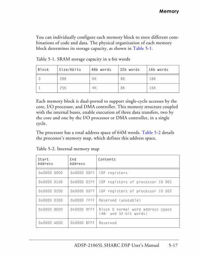
ADSP-21065L SHARC DSP User’s Manual 5-17
Memory
You can individually configure each memory block to store different com-binations of code and data. The physical organization of each memory block determines its storage capacity, as shown in Table 5-1.
Each memory block is dual-ported to support single-cycle accesses by the core, I/O processor, and DMA controller. This memory structure coupled with the internal buses, enable execution of three data transfers, two by the core and one by the I/O processor or DMA controller, in a single cycle.
The processor has a total address space of 64M words. Table 5-2 details the processor’s memory map, which defines this address space.
Table 5-1. SRAM storage capacity in x-bit words
Block Size/Kbits 48b words 32b words 16b words
0 288 6K 8K 18K
1 256 4K 8K 16K
Table 5-2. Internal memory map
Start Address
End Address
Contents
0x0000 0000 0x0000 00FF IOP registers
0x0000 0100 0x0000 01FF IOP registers of processor ID 001
0x0000 0200 0x0000 02FF IOP registers of processor ID 002
0x0000 0300 0x0000 7FFF Reserved (unusable)
0x0000 8000 0x0000 9FFF Block 0 normal word address space (48- and 32-bit words)
0x0000 A000 0x0000 BFFF Reserved
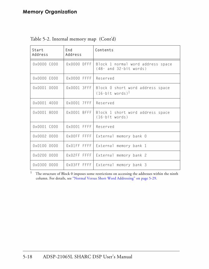
Memory Organization
5-18 ADSP-21065L SHARC DSP User’s Manual
0x0000 C000 0x0000 DFFF Block 1 normal word address space (48- and 32-bit words)
0x0000 E000 0x0000 FFFF Reserved
0x0001 0000 0x0001 3FFF Block 0 short word address space (16-bit words)1
0x0001 4000 0x0001 7FFF Reserved
0x0001 8000 0x0001 BFFF Block 1 short word address space (16-bit words)
0x0001 C000 0x0001 FFFF Reserved
0x0002 0000 0x00FF FFFF External memory bank 0
0x0100 0000 0x01FF FFFF External memory bank 1
0x0200 0000 0x02FF FFFF External memory bank 2
0x0300 0000 0x03FF FFFF External memory bank 3
1 The structure of Block 0 imposes some restrictions on accessing the addresses within the ninth column. For details, see “Normal Versus Short Word Addressing” on page 5-29.
Table 5-2. Internal memory map (Cont’d)
Start Address
End Address
Contents

ADSP-21065L SHARC DSP User’s Manual 5-19
Memory
The processor’s memory map is divided into three sections:
• Internal memory space
Corresponds to the processor’s IOP registers and normal word and short word addressing space.
The address boundaries for this space are:
0x0000 0000 to 0x0000 00FF IOP registers 0x0000 8000 to 0x0000 9FFF Block 0 normal0x0000 C000 to 0x0000 DFFF Block 1 normal0x0001 0000 to 0x0001 3FFF Block 0 short0x0001 8000 to 0x0001 BFFF Block 1 short
and, with reserved space interspersed between block segments at:
0x0000 A000 to 0x000 BFFF
0x0000 E000 to 0x000 FFFF
0x0001 4000 to 0x001 7FFF
0x0001 C000 to 0x001 FFFF
• Multiprocessor memory space
Corresponds to the IOP registers of the other processor in a multi-processor system.
The address boundary for this space is:
0x0000 0100 to 0x0000 02FF
• External memory space
Corresponds to off-chip memory and memory-mapped I/O devices.
The address boundary for this space is:
0x0002 0000 to 0x03FF FFFF

Memory Organization
5-20 ADSP-21065L SHARC DSP User’s Manual
Table 5-3 shows how the processor decodes and routes memory addresses over the DM and PM buses.
Table 5-3. Address decoding table for memory accesses
DM bit PM Bit Field Description
31-26 NA NA Reserved
25-24 NA V Virtual address.
00= Depends on E, S1-0, and M bits; address corresponds to local’s internal or external (Bank 0) memory or to remote processor’s IOP space.
01= External memory Bank 1, local processor
10= External memory Bank 2, local processor
11= External memory Bank 3, local processor
23-17 23-17 E Memory address.
00000[00] =Address in local or remote pro-cessor’s internal memory space.
xxxxx[xx] = Based on V bits; address in one of local’s four external memory banks.

ADSP-21065L SHARC DSP User’s Manual 5-21
Memory
16-15 16-15 S1 IOP register address (high order bits).
00= Based on M bits; address in local or remote processor’s IOP regis-ter
01= Normal word address in local’s internal memory
1x= Short word address in local’s internal memory
14-10 14-10 S0 IOP register address (low order bits).
00000 = Based on M bits; address in local or remote processor’s IOP regis-ter
xxxxx = Invalid if E or S bits =0s; oth-erwise, address in internal or external memory space (based on V, E, and S1 bits)
Table 5-3. Address decoding table for memory accesses (Cont’d)
DM bit PM Bit Field Description

Memory Organization
5-22 ADSP-21065L SHARC DSP User’s Manual
9-8 9-8 M IOP register space.
00= Address in local’s IOP register space
01= Address in IOP space of processor w/ID1
10= Address in IOP space of processor w/ID2
11= Invalid if E or S bits =0s; oth-erwise, address in internal or external memory space (based on V, E, and S1 bits)
7-0 7-0 P IOP register space address.
Table 5-3. Address decoding table for memory accesses (Cont’d)
DM bit PM Bit Field Description
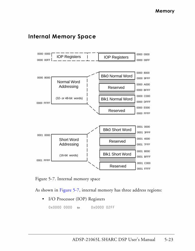
ADSP-21065L SHARC DSP User’s Manual 5-23
Memory
Internal Memory Space
Figure 5-7. Internal memory space
As shown in Figure 5-7, internal memory has three address regions:
• I/O Processor (IOP) Registers
0x0000 0000 to 0x0000 02FF
Short WordAddressing
(16-bit words)
0001 0000
0001 FFFF
Normal WordAddressing
(32- or 48-bit words)
0000 8000
0000 FFFF
0000 0000
0000 00FFIOP Registers
0000 0000
0000 00FFIOP Registers
Blk1 Normal Word
Blk0 Normal Word
Reserved
Reserved
0000 8000
0000 A000
0000 BFFF
0000 9FFF
0000 C000
0000 DFFF
0000 E000
0000 FFFF
Reserved
Blk0 Short Word
ReservedBlk1 Normal WordReserved
Blk1 Short Word
0001 0000
0001 4000
0001 7FFF
0001 3FFF
0001 8000
0001 BFFF
0001 C000
0001 FFFF

Memory Organization
5-24 ADSP-21065L SHARC DSP User’s Manual
The I/O Processor’s IOP registers are 256 memory-mapped regis-ters that control system configuration and various I/O operations. The address space between the IOP registers and normal word addresses—locations 0x0000 0300 to 0x0000 7FFF—is unusable memory, and applications should not write to it.
• Normal Word Addresses
Block 0 0x0000 8000 to 0x0000 9FFF
Block 1 0x0000 C000 to 0x0000 DFFF
The Interrupt Vector Table is located at the beginning of normal word addresses at:
0x0000 8000 to 0x0000 807F
• Short Word Addresses
Block 0 0x0001 0000 to 0x0001 3FFF
Block 1 0x0001 8000 to 0x0001 BFFF
Multiprocessor Memory Space
Figure 5-8. Multiprocessor memory space
Multiprocessor memory space maps to the IOP registers of the other ADSP-21065L in a multiprocessor system, enabling both processors to access the other’s memory-mapped IOP registers. On both processors, the
0000 0100
0000 01FF
0000 0100
0000 02FF 0000 0200
0000 02FF
MultiprocessorMemory Space
ID2 IOP Regs.
ID1 IOP Regs.

ADSP-21065L SHARC DSP User’s Manual 5-25
Memory
address range of the processor with ID1 is 0000 0100 to 0000 01FF, and the address range of the processor with ID2 is 0000 0200 to 0000 02FF.
As shown in Table 5-3 on page 5-20, when the E field of an address is zero and the M field is nonzero, the address falls within multiprocessor memory space. The value of M specifies the processor ID1-0 of the processor to access, and only that processor responds to the read or write cycle.
Instead of directly accessing its own internal memory, using its own ID, a processor can also access its memory through multiprocessor memory space. In this case, the core reads or writes to its own internal memory without accessing the external system bus. Only the processor’s core, not its DMA controller, can generate addresses for accessing its internal mem-ory through multiprocessor memory space.
If the processor attempts to access an invalid address in multiprocessor memory space, the other processor ignores written data and returns invalid data on a read.
For details on multiprocessor memory accesses, see Chapter 7, Multipro-cessing. For details on asynchronous accesses of multiple processors, see Chapter 8, Host Interface.
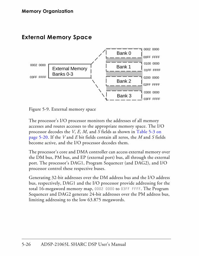
Memory Organization
5-26 ADSP-21065L SHARC DSP User’s Manual
External Memory Space
Figure 5-9. External memory space
The processor’s I/O processor monitors the addresses of all memory accesses and routes accesses to the appropriate memory space. The I/O processor decodes the V, E, M, and S fields as shown in Table 5-3 on page 5-20. If the V and E bit fields contain all zeros, the M and S fields become active, and the I/O processor decodes them.
The processor’s core and DMA controller can access external memory over the DM bus, PM bus, and EP (external port) bus, all through the external port. The processor’s DAG1, Program Sequencer (and DAG2), and I/O processor control these respective buses.
Generating 32-bit addresses over the DM address bus and the I/O address bus, respectively, DAG1 and the I/O processor provide addressing for the total 16-megaword memory map, 0002 0000 to 03FF FFFF. The Program Sequencer and DAG2 generate 24-bit addresses over the PM address bus, limiting addressing to the low 63.875 megawords.
0002 0000
0100 0000
01FF FFFFExternal MemoryBanks 0-3
0002 0000
03FF FFFF
00FF FFFF
0200 0000
02FF FFFF
0300 0000
03FF FFFF
Bank 0
Bank 3
Bank 2
Bank 1

ADSP-21065L SHARC DSP User’s Manual 5-27
Memory
Memory Space Access RestrictionsFollowing some basic rules, applications can use the processor’s three internal buses, PM, DM, and I/O, to access the processor’s memory map:
• The DM bus can access all memory spaces.
• The PM bus can access internal memory space and the lowest 63.875 megawords of external memory space only.
• The I/O bus can access all memory spaces except for the mem-ory-mapped IOP registers in internal memory space.

Word Size and Memory Block Organization
5-28 ADSP-21065L SHARC DSP User’s Manual
Word Size and Memory Block Organization
The processor’s internal memory accommodates the following word types:
• 48-bit instructions
• 40-bit extended precision, floating-point
These data are accessed in 48-bit words, with the 40 bits left-justi-fied in the 48-bit word (bits 47:8).
• 32-bit floating-point data
• 16-bit short word data
When the processor’s core accesses its internal memory, these rules deter-mine the word width of the access:
• Instruction fetches always read 48-bit words.
• Reads and writes using normal word addressing are either 32-or 48-bit words, depending on the memory block’s configuration in the SYSCON register.
• Reads and writes using short word addressing are always 16-bit words.
• PM bus (DAG2) reads and writes of the PX register are always 48-bit words, unless they use short word addressing.
• DM bus (DAG1) reads and writes of the PX register are always 40-bit words, unless they use short word addressing.

ADSP-21065L SHARC DSP User’s Manual 5-29
Memory
Normal Versus Short Word AddressingApplications can access the processor’s 544K bits of on-chip memory with either normal or short word addressing or with combinations of both.
When each word is 32 bits wide, the range of normal word addresses on each block is 8K words (16K words combined). In this configuration, however, some physical locations at the end of Block 0 become nonexist-ent. When each word is 48 bits wide, the range of normal word addresses on Block 0 is 6K words and on Block 1, 4K words (10K words combined). In this configuration, however, some physical locations at the end of Block 1 become nonexistent. For details on the physical mapping of 48-and 32-bit words, see “Mixing 32- and 48-Bit Words in One Memory Block” on page 5-32.
When each word is 16 bits wide, the range of short word addresses on Block 0 is 18K words and on Block 1, 16K words (34K words combined). On Block 0, however, the address range of the ninth column is noncontig-uous with the address range of the other eight columns. To address the ninth column for short word accesses, you must use the odd addresses between 0x14001 and 0x14FFF only. Even addresses between 0x14001 and 0x14FFF are undefined.
The PM and DM buses support both normal and short word addressing. Short word addressing increases the amount of 16-bit data that internal memory can store, and it enables MSW (most significant word) and LSW (least significant word) addressing format for 32-bit data words. Short word addressing of 16-bit data words is useful in array signal processing
Use caution when accessing the same physical location in mem-ory with both 32-and 48-bit words. For details, see “Interacting with the Shadow Write FIFO” on page 5-39.
Word Size and Memory Block Organization
5-30 ADSP-21065L SHARC DSP User’s Manual
systems. When it reads them from memory, depending on the SSE (short word sign-extension enable) bit in the MODE1 register, the processor either sign- extends or zero-fills 16-bit short words to 32-bit integers.
When configured for booting, the processor’s interrupt vector table is located at the start of normal word addressing, 0x0000 8000 –
0x0000 807F. When configured for “no boot” mode, the interrupt vector table is located in external memory, 0x0002 0000 to 0x0002 007F. If the IIVT (internal interrupt vector table) bit of the SYSCON register is set, the interrupt table resides in internal memory, regardless of the booting mode.
Using 32- and 48-Bit Memory WordsBecause each memory block is divided into columns that are 16-bits wide, 48-bit instruction words require three columns of contiguous memory, and 32-bit data words require two columns of contiguous memory. Six-teen-bit data words require one column.
Accordingly , the word width of an access determines how columns are grouped and how they are addressed for memory reads and writes.
For 48-bit instruction words, the access selects columns in groups of three. So, depending on the memory block accessed, a memory block consisting entirely of 48-bit instruction words has either three or two groups from which to select:
9 columns ÷ 3 columns per group = 3 groups (Block 0)
or
8 columns ÷ 3 columns per group = 2 groups (Block 1)
ADSP-21065L SHARC DSP User’s Manual 5-31
Memory
For Block 1, the last two columns are unused. So, a memory block that consists entirely of 48-bit words provides instruction storage for:
2K × 3 groups = 6K words (Block 0)
or
2K × 2 groups = 4K words (Block 1)
For 32-bit data words, the access selects columns in groups of two. So, a memory block consisting entirely of 32-bit data words has four groups to select from:
9 columns ÷ 2 columns per group = 4 groups (Block 0)
or
8 columns ÷ 2 columns per group = 4 groups (Block 1)
For Block 0, the last column is unused. So, a memory block that consists entirely of 32-bit data words provides instruction storage for:
2K × 4 groups = 8K words (Block 0 or Block 1)
Figure 5-11 on page 5-33 shows memory block configuration for four basic combinations of 32-bit data and 48-bit instructions.
Because the memory on the processor is arranged in eight and nine 16-bit columns, a similar set of calculations for 16-bit short words yields:
2K × 9 groups = 18K words of instruction storage
2K × 8 groups = 16K words of data storage
Figure 5-10 shows the ordering of 16-bit words within both 48-and 32-bit words and the initial addresses for each column of processor memory. All addresses indicate the first location of each column.
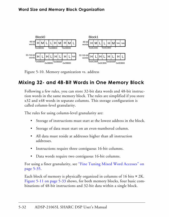
Word Size and Memory Block Organization
5-32 ADSP-21065L SHARC DSP User’s Manual
Figure 5-10. Memory organization vs. address
Mixing 32- and 48-Bit Words in One Memory BlockFollowing a few rules, you can store 32-bit data words and 48-bit instruc-tion words in the same memory block. The rules are simplified if you store x32 and x48 words in separate columns. This storage configuration is called column-level granularity.
The rules for using column-level granularity are:
• Storage of instructions must start at the lowest address in the block.
• Storage of data must start on an even-numbered column.
• All data must reside at addresses higher than all instruction addresses.
• Instructions require three contiguous 16-bit columns.
• Data words require two contiguous 16-bit columns.
For using a finer granularity, see “Fine Tuning Mixed Word Accesses” on page 5-35.
Each block of memory is physically organized in columns of 16 bits × 2K. Figure 5-11 on page 5-33 shows, for both memory blocks, four basic com-binations of 48-bit instructions and 32-bit data within a single block.
H M L H ML H M L0x08000 0x090000x08800
H HHL H L LL
0x088000x08000 0x09000
0x09800
32-/16-bitwords
32-/16-bitwords
Block0 Block148-bitwords H M L H ML NA
0x0C000 0x0C800
H HHL H L LL
0x0C8000x0C000 0x0D000
0x0D800
48-bitwords NA
NA

ADSP-21065L SHARC DSP User’s Manual 5-33
Memory
Figure 5-11. Example using words of mixed-length
A Three columns for instructions, four columns for data, and two unused columns, one between the 48-bit instructions and the 32-bit data and one at the end of the 32-bit data.
This configuration provides 2K of instruction storage and 4K of data storage. Column three is unused because the 32-bit data words must start on an even-numbered column, and column eight is unused because 32-bit data requires two columns.
1 2 3 4 5 6 7 8 9
1 2 3 4 5 6 7 8 9
32-bit data48-bit instructions
2x2 columns4K
32-bit data48-bit instructions
2 columns2K
3 columns2K
1 2 3 4 5 6 7 8
1 2 3 4 5 6 7 8
32-bit data48-bit instructions
32-bit data48-bit instructions
3 columns2K
2x2 columns4K
2 columns2K
2x3 columns4K
2x3 columns4K
BLOCK 1
BLOCK 0
A
B
C
D

Word Size and Memory Block Organization
5-34 ADSP-21065L SHARC DSP User’s Manual
B Six columns for instructions and two columns for data.
This configuration provides 4K of instruction storage and 2K of data storage.
C Three columns for instructions, four columns for data, and one unused column between the 48-bit instructions and the 32-bit data.
This configuration provides 2K of instruction storage and 4K of data storage. Column three is unused because the 32-bit data words must start on an even column number.
D Six columns for instructions and two columns for data.
This configuration provides 4K of instruction storage and 2K of data storage.
Table 5-4 shows the addressing in Block 0 (beginning address = 0x0000 8000) and in Block 1 (beginning address = 0x0000 C000) for each of the instruction and data combinations of Figure 5-11 on page 5-33.
Table 5-4. Address ranges for instructions and data
48-Bit Instructions 32-Bit Data
Start End Start End
A 0x0000 8000 0x0000 87FF 0x0000 9000 0x0000 9FFF
B 0x0000 8000 0x0000 8FFF 0x0000 9800 0x0000 9FFF
C 0x0000 C000 0x0000 C7FF 0x0000 D000 0x0000 DFFF
D 0x0000 C000 0x0000 CFFF 0x0000 D800 0x0000 DFFF

ADSP-21065L SHARC DSP User’s Manual 5-35
Memory
To determine the starting address of the 32-bit data, use the equations in Table 5-5.
Fine Tuning Mixed Word AccessesIf you must mix 48-bit instructions and 32-bit data words with finer gran-ularity than previously described, you need an in-depth understanding of the processor’s internal memory. This section details the low-level organi-zation and addressing of the internal memory blocks.
Low-Level Physical Mapping of Memory Blocks
Each block of memory is organized into columns that are 16-bits wide and 2K high, enabling each column to contain 2K 16-bit words. Block 0 con-tains nine columns, and Block 1 contains eight columns.
For reads or writes of 48-bit and 32-bit words, the thirteen LSBs of the address select a row from each column. The MSBs of the address control which columns are selected. For reads or writes of 16-bit short words, the address is right-shifted one place before it’s applied to memory (see Figure 5-12 on page 5-36). This frees bit 0 of the address to select between the MSW and LSW format of 32-bit data.
Table 5-5. Equation for determining the starting address of 32-bit data
Starting Address
B + m + 2048 + (2048 * i) + 1
B =beginning address of memory blockn =number of 48-bit instruction word locationsi =integer portion of [(n − 1) ÷ 2048]m =(n − 1) mod 2048

Word Size and Memory Block Organization
5-36 ADSP-21065L SHARC DSP User’s Manual
For any access, the word width of the access determines which columns are selected. For 48-bit words, the columns are selected in groups of three, and address bits 13:15 select the group. For 32-bit words, the columns are selected in groups of two, and address bits 13:15 select the group.
16-bit short word accesses are handled differently to provide easy access to the MSW and LSW of 32-bit data. In the processor’s DAGs, a single arithmetic right shift of the short word address provides the physical address of the destination 32-bit word. If the value of the bit shifted out is zero (0), the access is to the LSW, otherwise it is to the MSW. To imple-ment this, first you select columns in groups of two with address bits 13:15 and then select between the two columns in the group with the short word address bit shifted out.
Figure 5-12. Preprocessing 16-bit short word addresses
Restrictions on Storing Mixed Words
Although they are grouped differently within a memory block, 48-bit and 32-bit words attempt to use the same address area. This can cause errors when an application mixes 48-bit instructions and 32-bit data within the same block. (Since 32-bit and 16-bit words use the same grouping struc-ture but different addresses, an application can freely mix them within the
15 01213
1110 0001
31 24 17 16 15 0
BlockSelect
ColumnAddress
Row Address
Shift Right
High/LowWord (16-bit) Select
Short WordAddress
Physical AddressApplied toMemory Block

ADSP-21065L SHARC DSP User’s Manual 5-37
Memory
same memory block.) Remember that storing all 48-bit instructions at addresses lower than all 32-bit data prevents one overlapping the other.
Figure 5-13 on page 5-38 shows how 48-bit words fill a memory block and exactly where you can place 32-bit words. If the number of 48-bit word locations to allocate is n and the beginning address of the block is B, Table 5-6 shows the address where contiguous 32-bit data can begin.
Figure 5-13 on page 5-38 also shows that when 48-bit and 32-bit data are mixed in the same block with finer than column-level granularity, usable but discontiguous blocks of 32-bit memory are created.
Table 5-6. Starting address for contiguous 32-bit data
(n–1) ÷ 2048 Contiguous 32b DataStart Address
0 B + 2K m + 1
1 B + 4K m + 1
B = Beginning address of memory blockn = Number of 32b data word locationsm = (n – 1) mod 2048
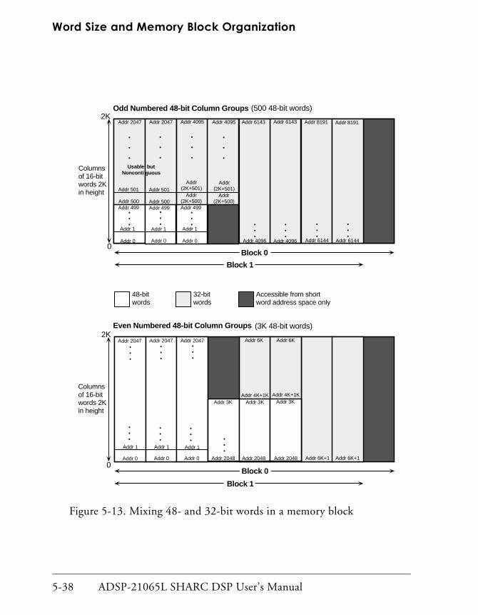
Word Size and Memory Block Organization
5-38 ADSP-21065L SHARC DSP User’s Manual
Figure 5-13. Mixing 48- and 32-bit words in a memory block
0
2K
Addr 0
Addr 2047 Addr 6K
Addr 2048
Addr 1
.
.
.
Addr 2047Addr 2047 Addr 6K
Addr 3K Addr 3KAddr 3KAddr 4K+1K Addr 4K+1K
Addr 6K+1 Addr 6K+1Addr 2048Addr 2048Addr 0Addr 0
Addr 1 Addr 1
.
.
.... .
.
.
.
.
....
.
.
.
Block 1
Block 0
0
Addr 20472K
.
.
.
Addr 501
Addr 500Addr 499
Addr 1
Addr 0
.
.
.
Addr 2047
.
.
.
Addr 501
Addr 500Addr 499
Addr 1
Addr 0
.
.
.
Addr 4095
.
.
.
Addr(2K+501)
Addr(2K+500)Addr 499
Addr 1
Addr 0
.
.
.
Addr 4095
.
.
.
Addr(2K+501)
Addr(2K+500)
Addr 6143 Addr 6143 Addr 8191Addr 8191
Addr 4096 Addr 4096 Addr 6144 Addr 6144
.
.
....
.
.
....
Block 0
Usable butNonconti guous
Block 1
32-bitwords
48-bitwords
Accessible from shortword address space only
Odd Numbered 48-bit Column Groups
Even Numbered 48-bit Column Groups
(500 48-bit words)
(3K 48-bit words)
Columnsof 16-bitwords 2Kin height
Columnsof 16-bitwords 2Kin height

ADSP-21065L SHARC DSP User’s Manual 5-39
Memory
To use all of the memory block, allocate 48-bit words in 4K word incre-ments (six columns). Even when all memory is used, a range of addresses that does not access any valid word exists between the 48-bit word region and the contiguous 32-bit word region.
To mix 16-bit words with 48-bit words, map the 16-bit words into 32-bit word space, and allocate memory for 32-bit words using the same method described here.
Interacting with the Shadow Write FIFO
Because the processor’s internal memory must operate at high speeds, writes to the memory do not go directly into the memory array, but instead into the Shadow Write FIFO.
The Shadow Write FIFO is a cache that temporarily stores the I/O proces-sor’s or core’s last two data writes before transferring them into internal memory. It stores the data and an address tag that corresponds to the data’s location in internal memory. Caching increases the speed at which internal memory operates.
When an internal memory write cycle occurs, the Shadow Write FIFO loads the data at the top (data from the first of two previous reads) into memory and loads the new data into the bottom. This operation is nor-mally transparent since the Shadow Write FIFO intercepts and temporarily stores any reads of the last two locations written. You need be aware of the Shadow Write FIFO only when you mix 48-bit and 32-bit word accesses to the same locations in memory.
The Shadow Write FIFO cannot differentiate between the mapping of 48-bit words and the mapping of 32-bit words. (See Figure 5-10 on page 5-32.) So, if you write a 48-bit word to memory and then try to read the data with a 32-bit word access, the Shadow Write FIFO will not intercept the read and will return incorrect data.
Word Size and Memory Block Organization
5-40 ADSP-21065L SHARC DSP User’s Manual
If you must mix 48-bit accesses and 32-bit accesses to the same locations this way, flush the Shadow Write FIFO with two dummy writes before you attempt to read the data.
Configuring Memory for 32- or 40-Bit Data You can configure each block of internal memory to store either sin-gle-precision 32-bit data or extended-precision 40-bit data. To configure data storage, set the IMDWx bits, IMDW0 and IMDW1, in the SYSCON register. If IMDWx = 0, the processor performs 32-bit data accesses. If IMDWx = 1, the processor performs 40-bit data accesses.
If an application attempts to write 40-bit data from a 48-bit word to a memory block configured for 32-bit data, the processor truncates the lower sixteen bits of the 48-bit word. Similarly, on an attempt to read 40-bit data, the processor fills the lower eight bits of the data with zeros. The only exception to these rules occurs in transfers involving the PX register.
For all reads and writes of the PX register, the processor performs 48-bit accesses. If you must store any 40-bit data in a memory block configured for 32-bit words, use the PX register to access the 40-bit data in 48-bit words. For 48-bit writes of 40-bit data from the PX register to 32-bit memory, make sure that the physical memory space of the 48-bit destina-tion does not corrupt any 32-bit data.
You can change the value of the IMDWx bits during system operation, but doing so affects all types of memory access, including processor–to–processor reads and writes, host–to–processor reads and writes, DMA transfers, and interrupt data areas.

ADSP-21065L SHARC DSP User’s Manual 5-41
Memory
Because the processor’s memory blocks must store either 32-bit or 40-bit data, DMA transfers automatically read or write the proper word width. This simplifies setting up DMA channels for a system. DMA transfers between serial ports and memory are limited to a maximum 32-bit word width.
Using 16-Bit Short Word AccessesBoth 32-bit data accesses and 48-bit instruction fetches must use normal word addressing. But 16-bit data accesses can use short word addressing.
Short word addressing increases the amount of 16-bit data that the proces-sor can store in internal memory, and it enables MSW (most significant word) and LSW (least significant word) addressing of 32-bit words. Bit 0 of the address selects between MSW and LSW addressing of 32-bit words.
Applications can access a single location in memory (that is, the lower 16 bits of a 32-bit word) using normal word addressing or short word addressing. The short word address is a left shift of the corresponding nor-mal word address. This enables easy conversion between short word addresses and normal word addresses for the same physical location.
The word width of data accesses and the value of the arithmetic precision mode bit RND32 are unrelated. This enables occa-sional use of 32-bit data in extended-precision, 40-bit systems, without having to toggle the value of RND32.
You can mix 32-bit words and 16-bit short words in the same memory block with no restrictions.
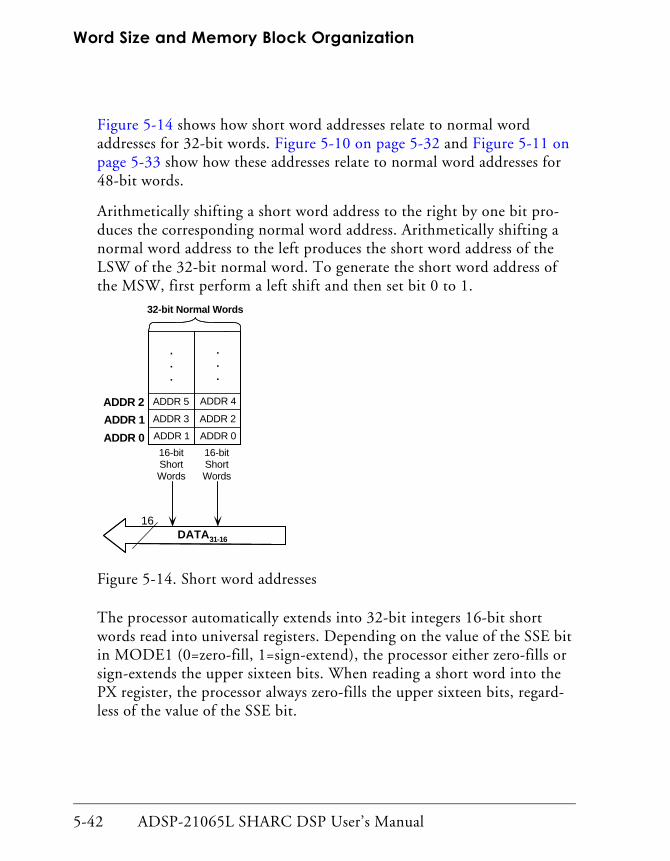
Word Size and Memory Block Organization
5-42 ADSP-21065L SHARC DSP User’s Manual
Figure 5-14 shows how short word addresses relate to normal word addresses for 32-bit words. Figure 5-10 on page 5-32 and Figure 5-11 on page 5-33 show how these addresses relate to normal word addresses for 48-bit words.
Arithmetically shifting a short word address to the right by one bit pro-duces the corresponding normal word address. Arithmetically shifting a normal word address to the left produces the short word address of the LSW of the 32-bit normal word. To generate the short word address of the MSW, first perform a left shift and then set bit 0 to 1.
Figure 5-14. Short word addresses
The processor automatically extends into 32-bit integers 16-bit short words read into universal registers. Depending on the value of the SSE bit in MODE1 (0=zero-fill, 1=sign-extend), the processor either zero-fills or sign-extends the upper sixteen bits. When reading a short word into the PX register, the processor always zero-fills the upper sixteen bits, regard-less of the value of the SSE bit.
ADDR 5
ADDR 3
ADDR 1
ADDR 4
ADDR 2
ADDR 0
ADDR 2
ADDR 1
ADDR 0
.
.
.
.
.
.
DATA31-16
16
16-bitShortWords
16-bitShortWords
32-bit Normal Words
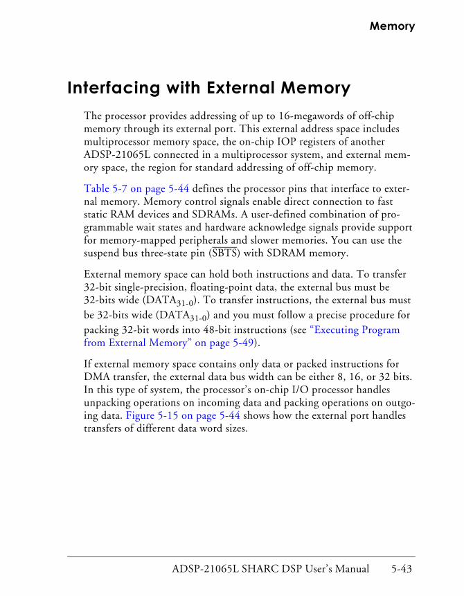
ADSP-21065L SHARC DSP User’s Manual 5-43
Memory
Interfacing with External MemoryThe processor provides addressing of up to 16-megawords of off-chip memory through its external port. This external address space includes multiprocessor memory space, the on-chip IOP registers of another ADSP-21065L connected in a multiprocessor system, and external mem-ory space, the region for standard addressing of off-chip memory.
Table 5-7 on page 5-44 defines the processor pins that interface to exter-nal memory. Memory control signals enable direct connection to fast static RAM devices and SDRAMs. A user-defined combination of pro-grammable wait states and hardware acknowledge signals provide support for memory-mapped peripherals and slower memories. You can use the suspend bus three-state pin (SBTS) with SDRAM memory.
External memory space can hold both instructions and data. To transfer 32-bit single-precision, floating-point data, the external bus must be 32-bits wide (DATA31-0). To transfer instructions, the external bus must be 32-bits wide (DATA31-0) and you must follow a precise procedure for packing 32-bit words into 48-bit instructions (see “Executing Program from External Memory” on page 5-49).
If external memory space contains only data or packed instructions for DMA transfer, the external data bus width can be either 8, 16, or 32 bits. In this type of system, the processor’s on-chip I/O processor handles unpacking operations on incoming data and packing operations on outgo-ing data. Figure 5-15 on page 5-44 shows how the external port handles transfers of different data word sizes.
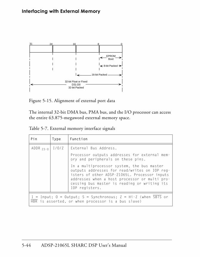
Interfacing with External Memory
5-44 ADSP-21065L SHARC DSP User’s Manual
Figure 5-15. Alignment of external port data
The internal 32-bit DMA bus, PMA bus, and the I/O processor can access the entire 63.875-megaword external memory space.
Table 5-7. External memory interface signals
Pin Type Function
ADDR 23-0 I/O/Z External Bus Address.
Processor outputs addresses for external mem-ory and peripherals on these pins.
In a multiprocessor system, the bus master outputs addresses for read/writes on IOP reg-isters of other ADSP-21065L. Processor inputs addresses when a host processor or multi pro-cessing bus master is reading or writing its IOP registers.
I = Input; O = Output; S = Synchronous; Z = Hi-Z (when SBTS or HBR is asserted, or when processor is a bus slave)
32-bit Float or FixedD31-D0
32-bit Packed
16-bit Packed
8-bit Packed
EPROMBoot
31 24 16 8 0
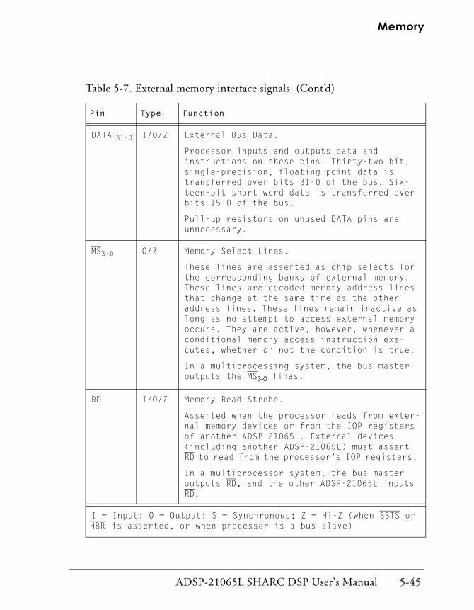
ADSP-21065L SHARC DSP User’s Manual 5-45
Memory
DATA 31-0 I/O/Z External Bus Data.
Processor inputs and outputs data and instructions on these pins. Thirty-two bit, single-precision, floating point data is transferred over bits 31-0 of the bus. Six-teen-bit short word data is transferred over bits 15-0 of the bus.
Pull-up resistors on unused DATA pins are unnecessary.
MS3-0 O/Z Memory Select Lines.
These lines are asserted as chip selects for the corresponding banks of external memory. These lines are decoded memory address lines that change at the same time as the other address lines. These lines remain inactive as long as no attempt to access external memory occurs. They are active, however, whenever a conditional memory access instruction exe-cutes, whether or not the condition is true.
In a multiprocessing system, the bus master outputs the MS3-0 lines.
RD I/O/Z Memory Read Strobe.
Asserted when the processor reads from exter-nal memory devices or from the IOP registers of another ADSP-21065L. External devices (including another ADSP-21065L) must assert RD to read from the processor’s IOP registers.
In a multiprocessor system, the bus master outputs RD, and the other ADSP-21065L inputs RD.
Table 5-7. External memory interface signals (Cont’d)
Pin Type Function
I = Input; O = Output; S = Synchronous; Z = Hi-Z (when SBTS or HBR is asserted, or when processor is a bus slave)
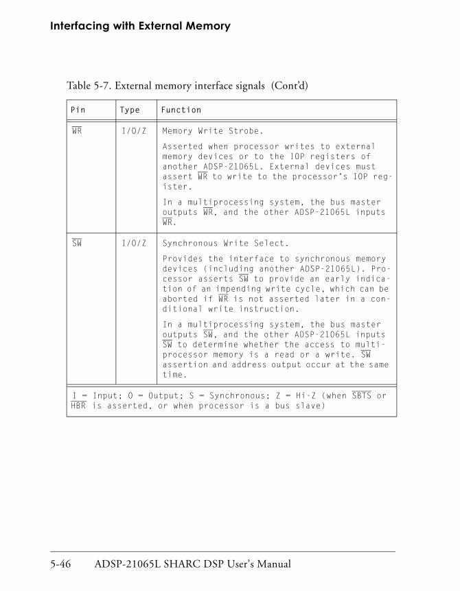
Interfacing with External Memory
5-46 ADSP-21065L SHARC DSP User’s Manual
WR I/O/Z Memory Write Strobe.
Asserted when processor writes to external memory devices or to the IOP registers of another ADSP-21065L. External devices must assert WR to write to the processor’s IOP reg-ister.
In a multiprocessing system, the bus master outputs WR, and the other ADSP-21065L inputs WR.
SW I/O/Z Synchronous Write Select.
Provides the interface to synchronous memory devices (including another ADSP-21065L). Pro-cessor asserts SW to provide an early indica-tion of an impending write cycle, which can be aborted if WR is not asserted later in a con-ditional write instruction.
In a multiprocessing system, the bus master outputs SW, and the other ADSP-21065L inputs SW to determine whether the access to multi-processor memory is a read or a write. SW assertion and address output occur at the same time.
Table 5-7. External memory interface signals (Cont’d)
Pin Type Function
I = Input; O = Output; S = Synchronous; Z = Hi-Z (when SBTS or HBR is asserted, or when processor is a bus slave)

ADSP-21065L SHARC DSP User’s Manual 5-47
Memory
ACK I/O/S Memory Acknowledge.
External devices can deassert ACK to add wait states to an external memory access. I/O devices, memory controllers, or other periph-erals use ACK to hold off completion of an access to external memory.
In a multiprocessing system, the slave pro-cessor deasserts the bus master’s ACK input to add wait states to an access of its internal memory. The bus master has a keeper latch on its ACK pin, which maintains the input at the level it was driven to last.
Table 5-7. External memory interface signals (Cont’d)
Pin Type Function
I = Input; O = Output; S = Synchronous; Z = Hi-Z (when SBTS or HBR is asserted, or when processor is a bus slave)
Interfacing with External Memory
5-48 ADSP-21065L SHARC DSP User’s Manual
External Memory BanksExternal memory is divided into four banks of fixed size. All banks, except bank 0, can address all 16M words of external memory. Because part of the first 16M words of external memory is in internal memory, bank 0 is limited to 15.875M words of address space.
Because of its size, bank 0 imposes limitations on some applications but not on others. For example, you wouldn’t want to use a 16M x 32 mem-ory in bank 0 because part of that address space is inaccessible. However, if you want to run code from external memory, you must do so from bank 0.
External memory’s extremely flexible architecture enables you to use any kind of memory in any bank. If you use SDRAM, you can map it to only one bank.
Because the size of the external memory banks is fixed, any address gener-ated within any external memory bank address space causes assertion of the corresponding MSx line. So, code your application to avoid generating addresses that do not map to physical devices.
Since all external memory space is banked, when you configure the blocks with bus idle, only transitions from reading one bank to reading another or to writing to the same bank generates an inactive bus cycle. Therefore, if you use several external devices, we recommend that you map each one to a different bank.
Each bank is associated with its own wait-state generator, enabling you to memory map slower peripheral devices into a bank that you have config-ured with a specific number of wait states. By mapping peripherals into different banks, you can accommodate I/O devices with different timing requirements. When you map SDRAM to a bank, make sure you program that bank with zero (0) wait states, so the SDRAM device operates properly.

ADSP-21065L SHARC DSP User’s Manual 5-49
Memory
Bank 0 starts at address 0x0002 0000 in external memory, followed by bank 1 at 0x0100 0000, bank 2 at 0x0200 0000, and bank 3 at 0x0300 0000. Whenever the processor generates an address located within one of the four banks, it asserts the corresponding memory select line, MS3-0.
You can use the MS3-0 outputs as chip selects for memories or for other external devices and eliminate the need for external decoding logic.
The MS3-0 lines are decoded memory address lines that change at the same time as the other address lines. While no external memory access is occur-ring, the MS3-0 lines are inactive. However, they are active during execution of a conditional memory access instruction, whether or not the condition is true. To ensure proper operation on systems that use the SW signal but are unable to abort such accesses, avoid using conditional mem-ory write instructions.
Executing Program from External MemoryTo execute 48-bit instructions from external memory, the processor packs 32-bit words in external memory into internal 48-bit instructions and vice versa. This kind of packing differs from the packing modes DMA control-ler accesses or host accesses use, and it is performed in these two cases only:
• The Program Sequencer initiates an external access to fetch an instruction.
• The processor loads data from external memory into the PX register.
The processor’s internal memory is divided into two blocks, but the external memory space is divided into four banks.
Interfacing with External Memory
5-50 ADSP-21065L SHARC DSP User’s Manual
Table 5-8 shows an example of the packing scheme the processor uses to store 48-bit instructions in external memory.
The processor stores an instruction in two consecutive internal memory locations, with the first sixteen of the forty-eight bit instruction in an even address, and the remaining thirty-two bits in the next location.
To generate a corresponding address in external memory for the first part of the instruction, the processor left-shifts bits 15:0 to generate bits 16:1 (ADDR16-0) in external memory. The processor leaves bits 23:17 unal-tered. Each access of external memory to fetch an instruction or to load the PX register translates into two accesses to successive locations. ADDR0 is 0 for the first access and 1 for the second. In this way, internal address 0x20000 on the PMA bus aligns with the beginning of external memory at 0x20000.
The processor supports program execution from external mem-ory bank 0 only.
Table 5-8. Example addresses for external program execution
Address/bits 31 bits 16 15 bits 0
0x20010 INSTR0[15:0]
0x20011 INSTR0[47:16]
0x20012 INSTR1[15:0]
0x20013 INSTR1[47:16]

ADSP-21065L SHARC DSP User’s Manual 5-51
Memory
To generate a corresponding address in external memory for the second part of the instruction, the processor increments the address of the previ-ous access by one.
Table 5-9 shows the address generation scheme. This scheme limits the size of the internal contiguous program segments to 64K.
On the PMA bus, 64K memory space maps to 128K memory space in x32 external memory. A program segment can start on any 128K boundary of external memory. Although the PMA bus provides only 64K of contigu-ous program memory space, to use multiple segments, programs can incorporate JUMP instructions towards the end of individual 64K segments.
As shown in Table 5-9, ranges of segmented addresses on the PMA bus give rise to continuous addresses in external memory. It is possible to entirely use up bank 0 (0x20000-0xFFFFFF) storing program.
Table 5-9. External memory address generation scheme
Segment PMA ADDR
1 0x20000
0x20001
0x2FFFF
6
4
K
0x20000/1
0x20002/3
0x3FFFE/F
1
2
8
K
2 0x40000
0x4FFFF
6
4
K
0x40000/1
0x5FFFE/F
1
2
8
K
Interfacing with External Memory
5-52 ADSP-21065L SHARC DSP User’s Manual
Program addresses in certain ranges are unavailable for program segments (for example, 0x30000-0x3FFFF), and some of these address regions may be unavailable for data segments too. This is so because any data access to a location (for example, 0x30000) occurs to a physical location where part of an instruction (0x28000 in this case) may be stored. Make sure you select data segments carefully to avoid corrupting program memory in external memory.
The processor drives the address for any data access as is on the ADDR pins, performing no packing. It does not support 40-bit data accesses from external memory. Programs must store 40-bit data in internal memory only.
3 0x60000
0x6FFFF
6
4
K
0x60000/1
0x7FFFE/F
1
2
8
K
.
.
.
.
.
.
.
.
.
.
.
.
.
.
.
The value in the bit position that corresponds to PM19-16 must be an even number. An odd numbered value in this position conflicts with valid segments.
Table 5-9. External memory address generation scheme (Cont’d)
Segment PMA ADDR

ADSP-21065L SHARC DSP User’s Manual 5-53
Memory
Boot Memory Select (BSEL and BMS)When BSEL is connected to VDD, BMS becomes an output pin, and the processor starts up in EPROM boot mode. The processor assumes that the EPROM’s data bus is 8-bits wide. For EPROM booting, make sure you connect BMS to the EPROM’s chip select pin and the EPROM and pro-cessor data buses together LSB to LSB. This configuration enables applications to access a separate external memory space for booting.
In EPROM boot mode, when the processor generates EPROM addresses, it:
• Uses the EBxWM and EBxWS bits in the WAIT register to config-ure wait states.
• Drives the MSx pins high.
Only the master processor drives BMS output. For details on EPROM booting, see Chapter 12, System Design.
Wait States and AcknowledgeYou use the processor’s WAIT register, an IOP control register, to config-ure external memory wait states and the processor’s response to the ACK signal.
To simplify the interface between the processor and slow external memo-ries and peripherals, the processor provides a variety of methods for extending off-chip memory accesses:
• External
The processor samples its acknowledge input (ACK) during each clock cycle.

Interfacing with External Memory
5-54 ADSP-21065L SHARC DSP User’s Manual
If it latches a low value, the processor inserts a wait state by holding the address and strobes valid for an additional cycle. If the value of ACK is high, the processor completes the cycle.
• Internal
The processor ignores the ACK input.
Control bits in the WAIT register specify the number of wait states for the access. You can specify a different number of wait states for each bank of external memory. The processor uses the 1x CLKIN to count the number of wait state cycles.
• Both
The processor samples its ACK input in each clock cycle.
If it latches a low value, the processor inserts a wait state. If the value of ACK is high, the processor completes the cycle only if the number of wait states (specified in WAIT) have expired.
In this mode, the WAIT-programmed wait states specify a mini-mum number of cycles per access, and an external device can use the ACK pin to extend the access as necessary. The ACK signal may be transitioning (be undefined) until the internally programmed wait states have finished; that is, the processor does not sample ACK until the programmed wait states have finished. No metastability problems will occur.
• Either
The processor completes the cycle as soon as it samples the ACK input as high or when the WAIT-programmed number of wait states have expired, whichever occurs first.
In this mode, a system with two different types of peripherals could use ACK to shorten the access for the faster peripheral and use the programmed wait states for the slower peripheral.

ADSP-21065L SHARC DSP User’s Manual 5-55
Memory
The method selected for one memory bank is independent of the method selected for any other bank. So, you can map devices of different speeds into different memory banks to maintain the appropriate wait state control.
The WAIT Register
The bits in the WAIT register enable you to configure:
• For each bank of external memory, the wait state mode.
• For each bank of external memory, the number of wait states.
• A single wait state for multiprocessor memory space.
• A single idle cycle for DMA Handshaking.
The WAIT register initializes to 0x21AD 6B5A after processor reset. This configures the processor for:
• Six internal wait states.
• Dependence on both software-programmed wait states and external acknowledge for all memory banks.
• Multiprocessor memory space wait state enabled. (For details, see “Multiprocessor Memory Space Wait States and Acknowledge” on page 5-61).
For proper SDRAM operation, make sure your application pro-grams a zero (EBxWS=000) wait state for the external memory bank to which it maps.
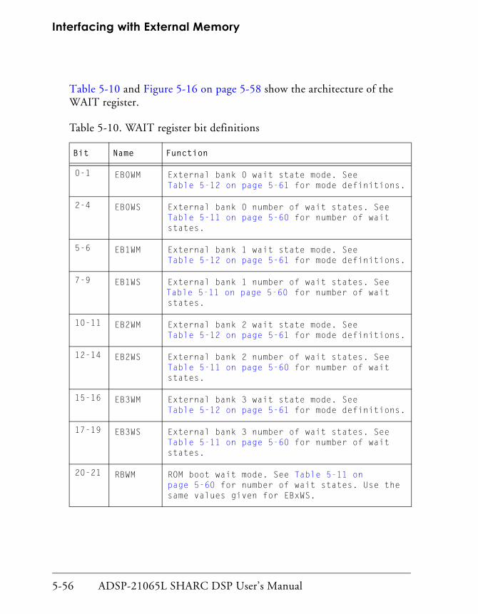
Interfacing with External Memory
5-56 ADSP-21065L SHARC DSP User’s Manual
Table 5-10 and Figure 5-16 on page 5-58 show the architecture of the WAIT register.
Table 5-10. WAIT register bit definitions
Bit Name Function
0-1 EB0WM External bank 0 wait state mode. See Table 5-12 on page 5-61 for mode definitions.
2-4 EB0WS External bank 0 number of wait states. See Table 5-11 on page 5-60 for number of wait states.
5-6 EB1WM External bank 1 wait state mode. See Table 5-12 on page 5-61 for mode definitions.
7-9 EB1WS External bank 1 number of wait states. See Table 5-11 on page 5-60 for number of wait states.
10-11 EB2WM External bank 2 wait state mode. See Table 5-12 on page 5-61 for mode definitions.
12-14 EB2WS External bank 2 number of wait states. See Table 5-11 on page 5-60 for number of wait states.
15-16 EB3WM External bank 3 wait state mode. See Table 5-12 on page 5-61 for mode definitions.
17-19 EB3WS External bank 3 number of wait states. See Table 5-11 on page 5-60 for number of wait states.
20-21 RBWM ROM boot wait mode. See Table 5-11 on page 5-60 for number of wait states. Use the same values given for EBxWS.
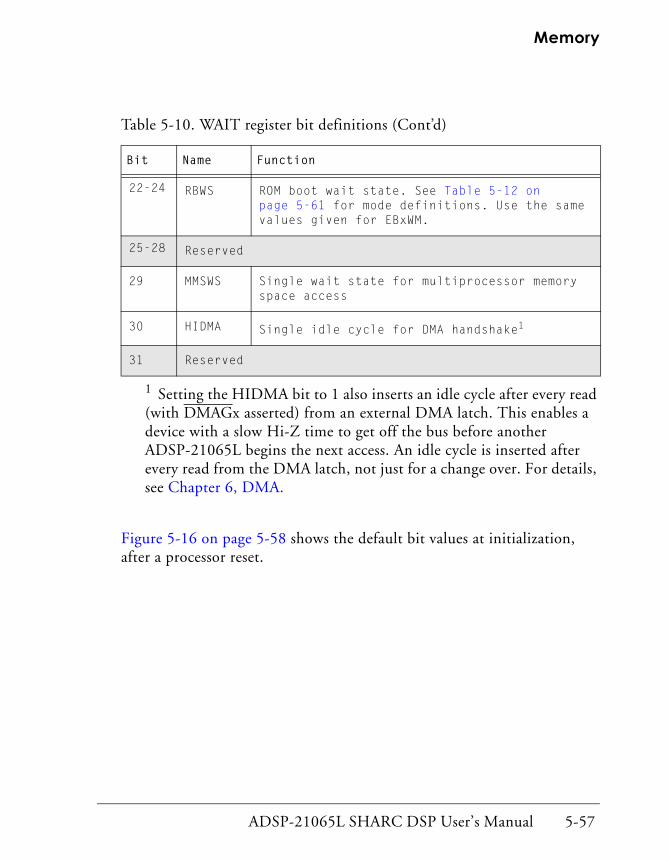
ADSP-21065L SHARC DSP User’s Manual 5-57
Memory
Figure 5-16 on page 5-58 shows the default bit values at initialization, after a processor reset.
22-24 RBWS ROM boot wait state. See Table 5-12 on page 5-61 for mode definitions. Use the same values given for EBxWM.
25-28 Reserved
29 MMSWS Single wait state for multiprocessor memory space access
30 HIDMA Single idle cycle for DMA handshake1
31 Reserved
1 Setting the HIDMA bit to 1 also inserts an idle cycle after every read (with DMAGx asserted) from an external DMA latch. This enables a device with a slow Hi-Z time to get off the bus before another ADSP-21065L begins the next access. An idle cycle is inserted after every read from the DMA latch, not just for a change over. For details, see Chapter 6, DMA.
Table 5-10. WAIT register bit definitions (Cont’d)
Bit Name Function
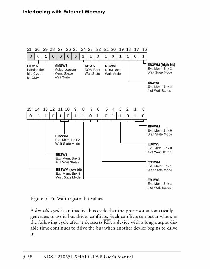
Interfacing with External Memory
5-58 ADSP-21065L SHARC DSP User’s Manual
Figure 5-16. Wait register bit values
A bus idle cycle is an inactive bus cycle that the processor automatically generates to avoid bus driver conflicts. Such conflicts can occur when, in the following cycle after it deasserts RD, a device with a long output dis-able time continues to drive the bus when another device begins to drive it.
31 30 29 28 27 26 25 24 23 22 21 20 19 18 17 16
0 0 00001 01101011 1
EB3WSExt. Mem. Bnk 3# of Wait States
EB3WM (high bit)Ext. Mem. Bnk 3Wait State Mode
HIDMAHandshakeIdle Cyclefor DMA
MMSWSMultiprocessorMem. SpaceWait State
15 14 13 12 11 10 9 8 7 6 5 4 3 2 1 0
0 1 10101 10110101 0
EB3WM (low bit)Ext. Mem. Bnk 3Wait State Mode
EB2WSExt. Mem. Bnk 2# of Wait States
EB2WMExt. Mem. Bnk 2Wait State Mode
EB1WSExt. Mem. Bnk 1# of Wait States
EB1WMExt. Mem. Bnk 1Wait State Mode
EB0WMExt. Mem. Bnk 0Wait State Mode
EB0WSExt. Mem. Bnk 0# of Wait States
RBWSROM BootWait State
RBWMROM BootWait Mode

ADSP-21065L SHARC DSP User’s Manual 5-59
Memory
To avoid this conflict, the processor generates bus idle cycle only on tran-sitions from reading one bank to reading another or to writing to the same bank. In other words, a bus idle cycle is generated after a read, except in the case of consecutive reads of the same bank. Normally, the processor’s bus idle cycle period is one full CLKIN cycle. When an SDRAM access occurs after an access that causes a bus idle cycle, however, the bus idle cycle period is only half of one CLKIN cycle.
Figure 5-17 shows the effects of the bus idle cycle option.
Figure 5-17. Bus idle cycle
For a device with a slow disable time, make sure your application enables bus idle cycle for the bank it uses. To do so, in the WAIT register, set the EBxWS bits for the particular bank as shown in Table 5-11 on page 5-60.
1xCLK
ADDRSWMS3-0
RD
WR
Access Bus Idle Cycle Read from different bank or write
Address changes
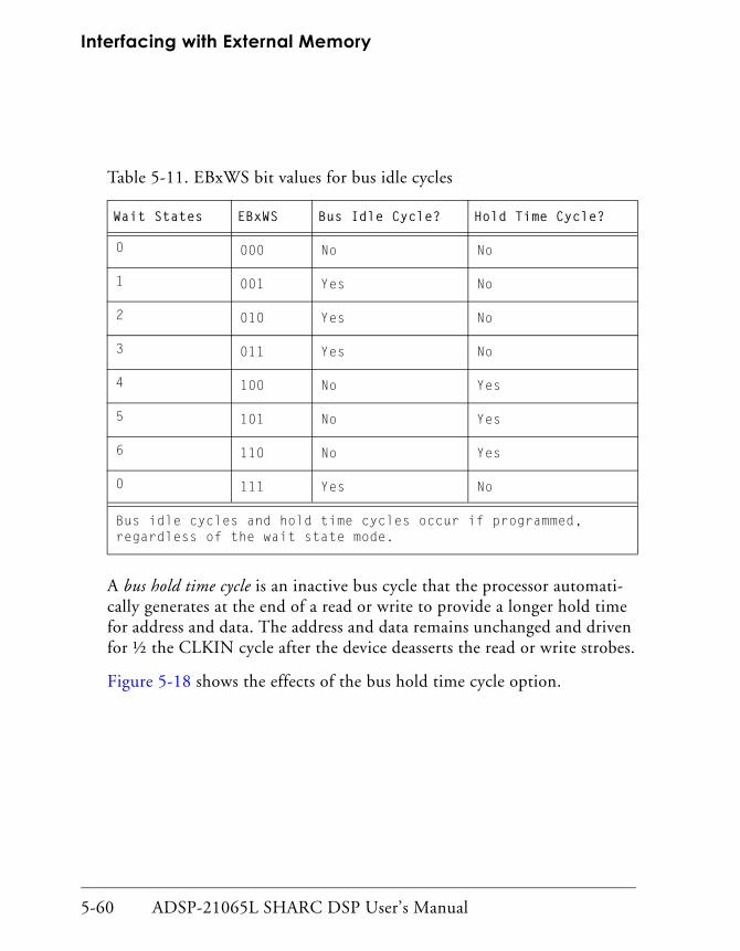
Interfacing with External Memory
5-60 ADSP-21065L SHARC DSP User’s Manual
A bus hold time cycle is an inactive bus cycle that the processor automati-cally generates at the end of a read or write to provide a longer hold time for address and data. The address and data remains unchanged and driven for ½ the CLKIN cycle after the device deasserts the read or write strobes.
Figure 5-18 shows the effects of the bus hold time cycle option.
Table 5-11. EBxWS bit values for bus idle cycles
Wait States EBxWS Bus Idle Cycle? Hold Time Cycle?
0 000 No No
1 001 Yes No
2 010 Yes No
3 011 Yes No
4 100 No Yes
5 101 No Yes
6 110 No Yes
0 111 Yes No
Bus idle cycles and hold time cycles occur if programmed, regardless of the wait state mode.
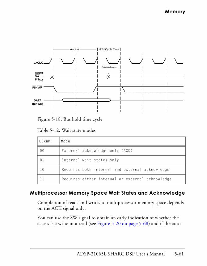
ADSP-21065L SHARC DSP User’s Manual 5-61
Memory
Figure 5-18. Bus hold time cycle
Multiprocessor Memory Space Wait States and Acknowledge
Completion of reads and writes to multiprocessor memory space depends on the ACK signal only.
You can use the SW signal to obtain an early indication of whether the access is a write or a read (see Figure 5-20 on page 5-68) and if the auto-
Table 5-12. Wait state modes
EBxWM Mode
00 External acknowledge only (ACK)
01 Internal wait states only
10 Requires both internal and external acknowledge
11 Requires either internal or external acknowledge
1xCLK
ADDRSWMS3-0
RD WR
Access Hold Cycle Time
Address changes
DATA(for WR)

Interfacing with External Memory
5-62 ADSP-21065L SHARC DSP User’s Manual
matic wait state option is enabled, adding a single wait state to all accesses of multiprocessor memory space.
To use the automatic wait state option, you set the MMSWS (multipro-cessor memory space wait state) bit in the WAIT register.
Use the automatic wait state option whenever the external system bus is heavily loaded—under conditions that prevent the system from meeting the synchronous timing requirements for interprocessor communications. See the processor’s data sheet for these specifications.
In this mode, the processors follow this procedure:
1. The master processor inserts the wait state.
2. In response, the slave processor drives ACK low in the first cycle, even if it has MMSWS=1.
If the master processor has MMSWS=1, it ignores ACK in the first cycle and responds to it in the second cycle. This setting provides longer set up times for the slave’s signals ADDR, RD, WR, and DATA (written to the slave). And it provides a longer set up time for the bus master’s ACK signal.
MMSWS=1 does not affect other set up and hold times. For example, it does not change hold times for the slave’s RD, WR, or DATA (written to the slave) or set up and hold times for the bus master’s DATA (read from the slave).
In a multiprocessor system, the value of the MMSWS bit must be the same on both processors.
ADSP-21065L SHARC DSP User’s Manual 5-63
Memory
External SDRAM MemoryApplications with large amounts of data can use off-chip SDRAM mem-ory for bulk storage. The processor’s SDRAM controller provides a glueless interface to standard 16M, 64M, and 128M SDRAMs. For details, see Chapter 10, SDRAM Interface.
Suspending Bus Three-state (SBTS)
External devices can assert the processor’s SBTS input to place the external bus address, data, selects, and strobes in a high-impedance state for the following cycle.
If the processor attempts to access external memory while SBTS is asserted, the processor halts, and the access to memory is delayed until the external device deasserts SBTS.
Use SBTS only to recover from deadlock with a host processor. (For details, see Chapter 8, Host Interface.)
SBTS causes the processor to place these pins in a high-impedance state.
Normal SBTS Operation: HBR not Asserted
Asserting SBTS places the external bus address, data, selects, and strobes in a high-impedance state for the following cycle.
If SBTS is asserted while an external access is in progress, the processor aborts the access (as if ACK were deasserted) and restarts the access after SBTS is deasserted.
• ADDR23-0 • BMS • DATA31-0
• DMAG2-1 • MS3-0 • RD
• SW • WR

Interfacing with External Memory
5-64 ADSP-21065L SHARC DSP User’s Manual
If SBTS is asserted while no external access is in progress, the processor puts the external bus pins in a high impedance state and continues run-ning until it initiates an external access (at which time the processor halts). In this case, the memory access begins in the cycle after the deassertion of SBTS.
When SBTS is deasserted, the processor reasserts the RD, WR, and DMAGx strobes (if they were asserted before) after the external address becomes valid (at normal timing within the cycle). The processor also resets the wait state counter, even if the processor is held in reset (RESET asserted).
SBTS differs from HBR since it takes effect in the next cycle, even if an external access is in progress (but not finished). Use SBTS only when accessing an external device, such as an SDRAM or cache memory, where the access must be held off to prepare for it. Using SBTS at other times—such as during ADSP-21065L-to-ADSP-21065L accesses or during asser-tion of DMAGx—results in incorrect operation.
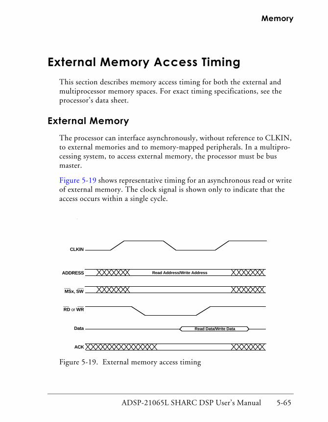
ADSP-21065L SHARC DSP User’s Manual 5-65
Memory
External Memory Access TimingThis section describes memory access timing for both the external and multiprocessor memory spaces. For exact timing specifications, see the processor’s data sheet.
External MemoryThe processor can interface asynchronously, without reference to CLKIN, to external memories and to memory-mapped peripherals. In a multipro-cessing system, to access external memory, the processor must be bus master.
Figure 5-19 shows representative timing for an asynchronous read or write of external memory. The clock signal is shown only to indicate that the access occurs within a single cycle.
Figure 5-19. External memory access timing
CLKIN
ADDRESS
ACK
RD or WR
MSx, SW
Data
Read Address/Write Address
Read Data/Write Data
External Memory Access Timing
5-66 ADSP-21065L SHARC DSP User’s Manual
Bus Master Reads of External Memory
External memory reads follow this sequence (see Figure 5-19):
1. The processor drives the read address and asserts a memory select signal (MS3-0) to indicate the selected bank.
The processor does not deassert the memory select signal between successive accesses of the same memory bank.
2. The processor asserts the read strobe (unless the access is aborted due to a conditional instruction).
3. The processor determines whether it needs to insert wait states.
If so, the memory select and read strobe remain active for one or more additional cycles. The state of the external acknowledge sig-nal (ACK), the internally programmed wait state count, or a combination of the two determine the wait states.
4. The processor latches in the data.
5. The processor deasserts the read strobe.
6. If initiating another memory access, the processor drives the address and memory select lines for the next cycle.
If a memory read is part of a conditional instruction that remains unexe-cuted because the condition is false, the processor still drives the address and memory select lines for the read, but it does not assert the read strobe or read any data.
ADSP-21065L SHARC DSP User’s Manual 5-67
Memory
Bus Master Writes of External Memory
External memory writes follow this sequence (see Figure 5-19 on page 5-65):
1. The processor drives the write address and asserts a memory select signal to indicate the selected bank.
The processor does not deassert the memory select signal between successive accesses of the same memory bank.
2. The processor asserts the write strobe and drives the data (unless the memory access is aborted due to a conditional instruction).
3. The processor determines whether it needs to insert wait states.
If so, the memory select and write strobe remain active for one or more additional cycles. The state of the external acknowledge sig-nal, the internally programmed wait state count, or a combination of the two determine the wait states.
4. The processor deasserts the write strobe near the end of the cycle.
5. The processor puts its data outputs in a high impedance state.
6. If initiating another memory access, the processor drives the address and memory select lines for the next cycle.
If a memory write is part of a conditional instruction that remains unexe-cuted because the condition is false, the processor still drives the address and memory select lines for the write, but it does not assert the write strobe or drive any data.
Multiprocessor MemoryFigure 5-20 on page 5-68 shows timing for multiprocessor memory accesses. For details on multiprocessor memory accesses, see Chapter 7, Multiprocessing.

External Memory Access Timing
5-68 ADSP-21065L SHARC DSP User’s Manual
Figure 5-20. Multiprocessor memory access timing
ADDRESS WriteAddr
ACK
WR
SW
Data Write Data
RD
Read Data
Read AddrWrite Addr
Write Data

ADSP-21065L SHARC DSP User’s Manual 6-1
6 DMAFigure 6-0.
Listing 6-0.
Table 6-0.
Table 6-0.
Direct Memory Access (DMA) provides a mechanism for transferring an entire block of data.
The processor’s on-chip DMA controller relieves the core processor of moving data between internal memory and an external data source or external memory. Fully integrated, the DMA controller enables the pro-cessor’s core or an external device to specify data transfer operations and return to normal processing while the DMA controller carries out data transfers independently and transparently.
The DMA controller can transfer blocks of data between:
• Internal memory and external memory or memory-mapped periph-erals
• Internal memory and the IOP registers of another ADSP-21065L
• Internal memory and a host
• Internal memory and serial port I/O
• External memory and external peripherals
To ensure compatibility between its internal 32- and 48-bit structure and 16- and 32-bit peripheral devices, the processor packs and unpacks exter-nal bus words.
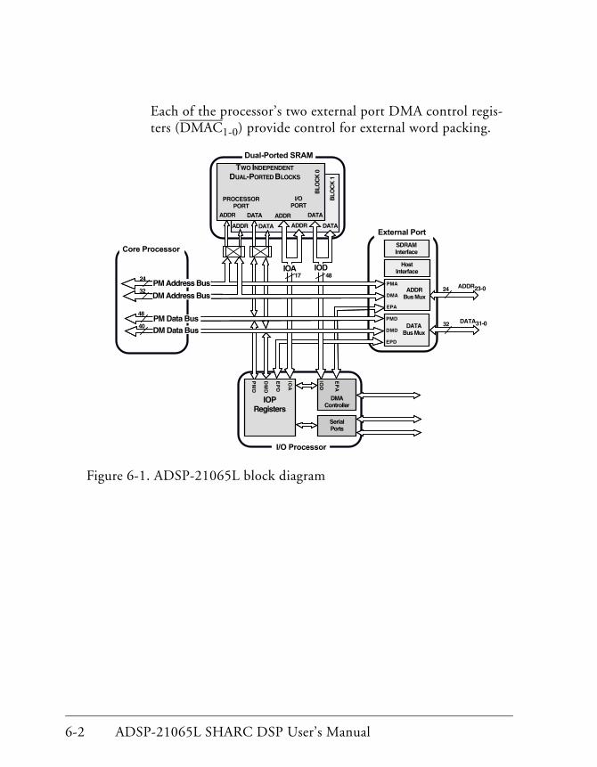
6-2 ADSP-21065L SHARC DSP User’s Manual
Each of the processor’s two external port DMA control regis-ters (DMAC1-0) provide control for external word packing.
Figure 6-1. ADSP-21065L block diagram
%%% %%%
.!
$
B
C ,+,,
%!2+,.!$B#
+$,##+
6+
% %% %%%
.!
$
B
)
)/
)
#%
9
%%.0
+
,+
%.0
+%
%
,+%
# +
+
%$
+%.
%.
+ .
.
)/ %
%%2
%2
)
%
,+
+
,+
%
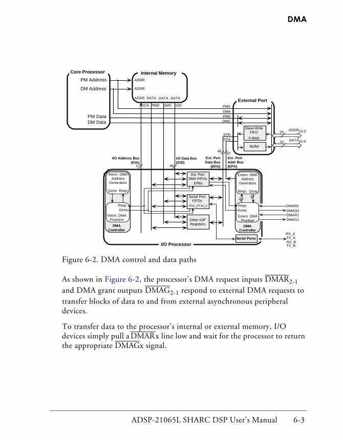
ADSP-21065L SHARC DSP User’s Manual 6-3
DMA
Figure 6-2. DMA control and data paths
As shown in Figure 6-2, the processor’s DMA request inputs DMAR2-1 and DMA grant outputs DMAG2-1 respond to external DMA requests to transfer blocks of data to and from external asynchronous peripheral devices.
To transfer data to the processor’s internal or external memory, I/O devices simply pull a DMARx line low and wait for the processor to return the appropriate DMAGx signal.
I/O Processor
Intern. DMAAddress
Generators
Grnts Reqs.
Intern. DMAPrioritzer
Reqs.Grnts
DMAController
Ext. PortDMA FIFOs
EPBx
Serial PortFIFOs
RXx_z/TXx_z
Other IOPRegisters
Extern. DMAAddress
Generators
GrntsReqs.
Extern. DMAPrioritzer
Reqs.Grnts
DMAController
Serial Ports
44
ADDR
DATA DATA
ADDR
Internal Memory
ADDR DATA
17
I/O Address Bus(IOA)
Core Processor
External Port
ADDR23-024
32 DATA31-0
PM Address
DM Address
PM DataDM Data
Slave WriteFIFO
4 deep
Buffer
48
I/O Data Bus(IOD)
48 32
PMADMA
DMDPMD
IOA IODPMD DMD
Ext. PortData Bus
(EPD)
EPAEPD
Ext. PortAddr Bus(EPA)
DMAR1DMAG1
DMAR0DMAG0
TX_ARX_A
RX_BTX_B
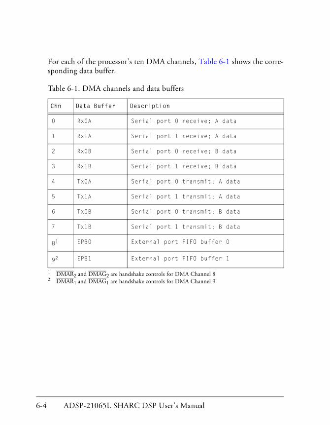
6-4 ADSP-21065L SHARC DSP User’s Manual
For each of the processor’s ten DMA channels, Table 6-1 shows the corre-sponding data buffer.
Table 6-1. DMA channels and data buffers
Chn Data Buffer Description
0 Rx0A Serial port 0 receive; A data
1 Rx1A Serial port 1 receive; A data
2 Rx0B Serial port 0 receive; B data
3 Rx1B Serial port 1 receive; B data
4 Tx0A Serial port 0 transmit; A data
5 Tx1A Serial port 1 transmit; A data
6 Tx0B Serial port 0 transmit; B data
7 Tx1B Serial port 1 transmit; B data
81
1 DMAR2 and DMAG2 are handshake controls for DMA Channel 8
EPB0 External port FIFO buffer 0
92
2 DMAR1 and DMAG1 are handshake controls for DMA Channel 9
EPB1 External port FIFO buffer 1

ADSP-21065L SHARC DSP User’s Manual 6-5
DMA
The following terms are used throughout this chapter:
External port FIFO buffersEPB1-0. The IOP registers used for external port DMA transfers and single-word data transfers from another ADSP-21065L or from a host. These buffers are 6-deep FIFOs.
DMACx control registersThe DMA control registers for the EPBx external port buffers DMAC1-0. These correspond to EPB1-0, respectively.
DMA parameter registersThe registers used to set up a DMA transfer. These registers include: address (IIx), modifier (IMx), count (Cx), chain pointer (CPx), and so on.
SPORTSerial port.
Transfer control block (TCB)A set of DMA parameter register values stored in internal memory that the processor’s DMA controller downloads for chained DMA operations.
TCB chain loadingThe process by which the processor’s DMA controller downloads a transmit control block from memory and autoinitializes the DMA parameter registers.

6-6 ADSP-21065L SHARC DSP User’s Manual
The following conventions of notation are used throughout this chapter:
In register names,
• x = SPORT number (0/1)
• y = transmit or receive (T/R)
• z = data channel (A/B).
For example, in the notation DMACx for a DMA control register, x = SPORT number.
In the notation TXx_z for a DMA data buffer:
• TX = Transmit data buffer
• x = 0 or 1 (SPORT)
• z = A or B (data channel)
In the notation IIyx_z for a DMA parameter register:
• II = Index register
• y = R or T (Receive or Transmit)
• x = 0 or 1 (SPORT)
• z = A or B (data channel)

ADSP-21065L SHARC DSP User’s Manual 6-7
DMA
DMA Controller OperationThe processor’s DMA controller performs four basic types of DMA trans-fer operations:
• External port block data transfers
This type of transfer moves data between the processor’s internal memory and external memory, a host, another processor, or a mem-ory-mapped device.
The application must program the DMA controller with the size and address of the internal memory buffer, the address increment, and the direction of transfer. The application may need to supply an external address also.
Once programmed, the DMA controller automatically begins trans-fers and continues until it has transferred the entire buffer to or from internal memory.
The processor supports four external port DMA transfer modes: master mode, handshake mode, external handshake mode, and paced master mode. For details, see “External Port DMA Modes” on page 6-55.
• Serial port I/O data transfers
This type of transfer handles data transmitted and received through the processor’s serial ports.
As with external port transfers, the application must configure an internal memory buffer, but the DMA controller accesses the Tx or Rx serial port buffer instead of the EPBx buffer.
The direction of the serial port determines the direction of the data transfer. When the port receives data, the DMA controller automat-ically transfers it to internal memory. Likewise, when the port must
DMA Controller Operation
6-8 ADSP-21065L SHARC DSP User’s Manual
transmit a word, the DMA controller automatically fetches the word from internal memory.
• Transfers between external devices and external memory.
The processor also supports data transfers between an external device and external memory. This type of transfer does not interfere with internal operations that do not use the external port.
External devices participate in DMA transfers in one of two ways:
• They read or write to one of the processor’s DMA buffers.
• They assert a DMA request input (DMARx) to request ser-vice.
• DMA chaining
Applications can program one DMA transfer operation, upon fin-ishing, to autoinitialize another one on the same channel.
ADSP-21065L SHARC DSP User’s Manual 6-9
DMA
Setting Up DMA TransfersThe master processor or a host can program DMA operations. To do so, the application must write to the processor’s memory-mapped DMA con-trol and parameter registers. This includes writing a set of memory buffer parameters to the DMA parameter registers and loading:
• The IIyx_z register with the starting address of the buffer.
• The IMyx_z register with an address modifier.
• The Cyx_z register with a word count.
Each external port and each serial port has a DMA enable bit (DEN) in its main control register (DMACx) that enables DMA operation. Once set up and enabled, DMA channels automatically transfer data words they receive to the buffer in internal memory. Likewise, when the processor is ready to transmit data, DMA channels automatically transfer data from internal memory to the DMA buffer register. Transfer continues until the entire data buffer has been received or transmitted.
The processor generates a DMA interrupt when it completes the transfer of an entire block of data. An interrupt occurs when the DMA channel’s count register Cyx_z (and ECEPx register in master mode only) decre-ments to zero (0). The processor latches and masks DMA interrupts in the IRPTL and IMASK registers, respectively. These registers are located in the processor’s core, not in its memory-mapped IOP register space.
To start a new DMA sequence after the current one finishes, applications must follow these steps:
1. Clear the DEN bit;
2. Write new parameters to the II, IM, and C registers;

Setting Up DMA Transfers
6-10 ADSP-21065L SHARC DSP User’s Manual
3. Set the DEN bit to re-enable DMA.
For chained DMA operations, this is not necessary. For details, see “DMA Chaining” on page 6-39.
ADSP-21065L SHARC DSP User’s Manual 6-11
DMA
DMA Control RegistersThe registers that control and configure DMA operations are part of the memory-mapped IOP register set. To access these registers, applications write to or read from the appropriate address in memory.
This section describes the various operating modes of the DMA controller and associated control registers and bits. For details on the IOP registers, see Appendix E, Control and Status Registers, in ADSP-21065L SHARC DSP Technical Reference.
Table 6-2 lists the DMA control registers and data buffer registers. Because the serial port DMA control bits are located in the SPORT con-trol registers, they do not appear in this table. For details, see “Serial Port DMA Control Registers” on page 6-22.
Table 6-2. DMA control, buffer, and parameter registers
Register Width Description
EPB0 48 External port DMA FIFO buffer 0
EPB1 48 External port DMA FIFO buffer 1
DMAC0 16 DMA channel 8 control register for Ext. port buffer 0 (EPB0)
DMAC1 16 DMA channel 9 control register for Ext. port buffer 1 (EPB1)
DMASTAT 32 DMA channel status register
IIR0A, IMR0A, CR0A, CPR0A, GPR0A
16-18 DMA channel 0 parameter registers (SPORT0 receive, A data)
IIR0B, IMR0B, CR0B, CPR0B, GPR0B
16-18 DMA channel 1 parameter registers (SPORT0 receive, B data)
DMA Control Registers
6-12 ADSP-21065L SHARC DSP User’s Manual
External Port DMA RegistersEach external port DMA channel has its own control register, DMACx (see Figure 6-3), that corresponds to either DMA channel 8 or 9.
All bits are active high unless otherwise noted.
IIR1A, IMR1A, CR1A, CPR1A, GPR1A
16-18 DMA channel 2 parameter registers (SPORT1 receive, A data)
IIR1B, IMR1B, CR1B, CPR1B, GPR1B
16-18 DMA channel 3 parameter registers (SPORT1 receive, B data)
IIT0A, IMT0A, CT0A, CPT0A, GPT0A
16-18 DMA channel 4 parameter registers (SPORT0 transmit, A data)
IIT0B, IMT0B, CT0B, CPT0B, GPT0B
16-18 DMA channel 5 parameter registers (SPORT0 transmit, B data)
IIT1A, IMT1A, CT1A, CPT1A, GPT1A
16-32 DMA channel 6 parameter registers (SPORT1 transmit, A data)
IIT1B, IMT1B, CT1B, CPT1B, GPT1B
16-32 DMA channel 7 parameter registers (SPORT1 transmit, B data)
IIEP0, IMEP0, CEP0, CPEP0, GPEP0, EIEP0, EMEP0, ECEP0
16-32 DMA channel 8 parameter registers (External port FIFO buffer 0)
IIEP1, IMEP1, CEP1, CPEP1, GPEP1, EIEP1, EMEP1, ECEP1
16-32 DMA channel 9 parameter registers (External port FIFO buffer 1)
Table 6-2. DMA control, buffer, and parameter registers (Cont’d)
Register Width Description

ADSP-21065L SHARC DSP User’s Manual 6-13
DMA
Figure 6-3. DMACx registers
31 30 29 28 27 26 25 24 23 22 21 20 19 18 17 16
0 0 00000 00000000 0
15 14 13 12 11 10 9 8 7 6 5 4 3 2 1 0
0 0 00000 00000000 0
FLSHFlush Ext. Port FIFO1=flush
EXTENExt. Devices toExt. Mem. DMA1=ext. mode
INTIOSingle-word Interrupts - ext. port FIFO0=disable1=enable
MASTERDMAMastermode0=disable1=enable
DENDMA Enable for ext. port0=disable1=enable
CHENDMA Chaining Enable for ext. port0=disable1=enable
TRANDMA chn. direction0=read from ext. mem.1=write to ext. mem.
FSExt. Port FIFO Status00=empty10=partially full11=full
PSPacking Status read-only00=packing done01=1st stage all modes10=2nd stage 16 to 48 mode or 32 to 48 mode
DTYPEData Type0=data1=instructions
PMODEPacking Mode00=no packing01=16/3210=16/4811=32/48
MSWFMost Significant Word First packing order0=disable1=enable
HSHAKEDMAHandshake0=disable1=enable
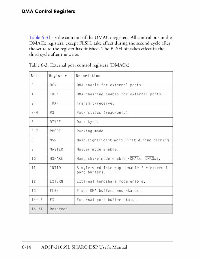
DMA Control Registers
6-14 ADSP-21065L SHARC DSP User’s Manual
Table 6-3 lists the contents of the DMACx registers. All control bits in the DMACx registers, except FLSH, take effect during the second cycle after the write to the register has finished. The FLSH bit takes effect in the third cycle after the write.
Table 6-3. External port control registers (DMACx)
Bits Register Description
0 DEN DMA enable for external ports.
1 CHEN DMA chaining enable for external ports.
2 TRAN Transmit/receive.
3-4 PS Pack status (read-only).
5 DTYPE Data type.
6-7 PMODE Packing mode.
8 MSWF Most significant word first during packing.
9 MASTER Master mode enable.
10 HSHAKE Hand shake mode enable (DMARx, DMAGx).
11 INTIO Single-word interrupt enable for external port buffers.
12 EXTERN External handshake mode enable.
13 FLSH Flush DMA buffers and status.
14-15 FS External port buffer status.
16-31 Reserved

ADSP-21065L SHARC DSP User’s Manual 6-15
DMA
DEN Enables DMA for the external port buffers.
CHENEnables chained DMA transfers.
Setting CHEN=1 and DEN=0 places the DMA channel in chain inser-tion mode. In this mode, the application can insert a new DMA chain into the current chain without affecting the current DMA transfer. This mode is similar to setting CHEN=1 and DEN=1, except it disables automatic chaining when the current DMA transfer ends.
Table 6-4 lists the modes selected by the CHEN and DEN bits.
TRANSpecifies the direction of data transfer.
TRAN = 1 Transmit; read from internal memory to EPBx (slave mode) or to the external bus through the EPBx buffers (master mode).
TRAN = 0 Receive; write to internal memory from the external bus through the EPBx buffers.
Table 6-4. CHEN and DEN modes
CHEN DEN Mode
0 0 Chaining disabled, DMA disabled
0 1 Chaining disabled, DMA enabled
1 0 Chaining enabled, DMA enabled, autochain-ing disabled (chain insertion mode)
1 1 Chaining enabled, DMA enabled, autochain-ing enabled
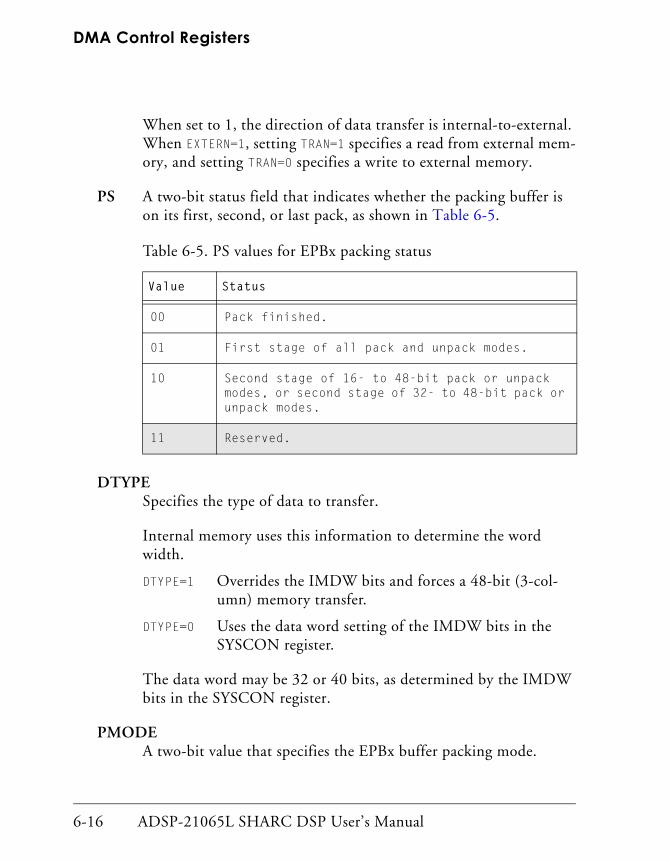
DMA Control Registers
6-16 ADSP-21065L SHARC DSP User’s Manual
When set to 1, the direction of data transfer is internal-to-external. When EXTERN=1, setting TRAN=1 specifies a read from external mem-ory, and setting TRAN=0 specifies a write to external memory.
PS A two-bit status field that indicates whether the packing buffer is on its first, second, or last pack, as shown in Table 6-5.
DTYPESpecifies the type of data to transfer.
Internal memory uses this information to determine the word width.
DTYPE=1 Overrides the IMDW bits and forces a 48-bit (3-col-umn) memory transfer.
DTYPE=0 Uses the data word setting of the IMDW bits in the SYSCON register.
The data word may be 32 or 40 bits, as determined by the IMDW bits in the SYSCON register.
PMODEA two-bit value that specifies the EPBx buffer packing mode.
Table 6-5. PS values for EPBx packing status
Value Status
00 Pack finished.
01 First stage of all pack and unpack modes.
10 Second stage of 16- to 48-bit pack or unpack modes, or second stage of 32- to 48-bit pack or unpack modes.
11 Reserved.
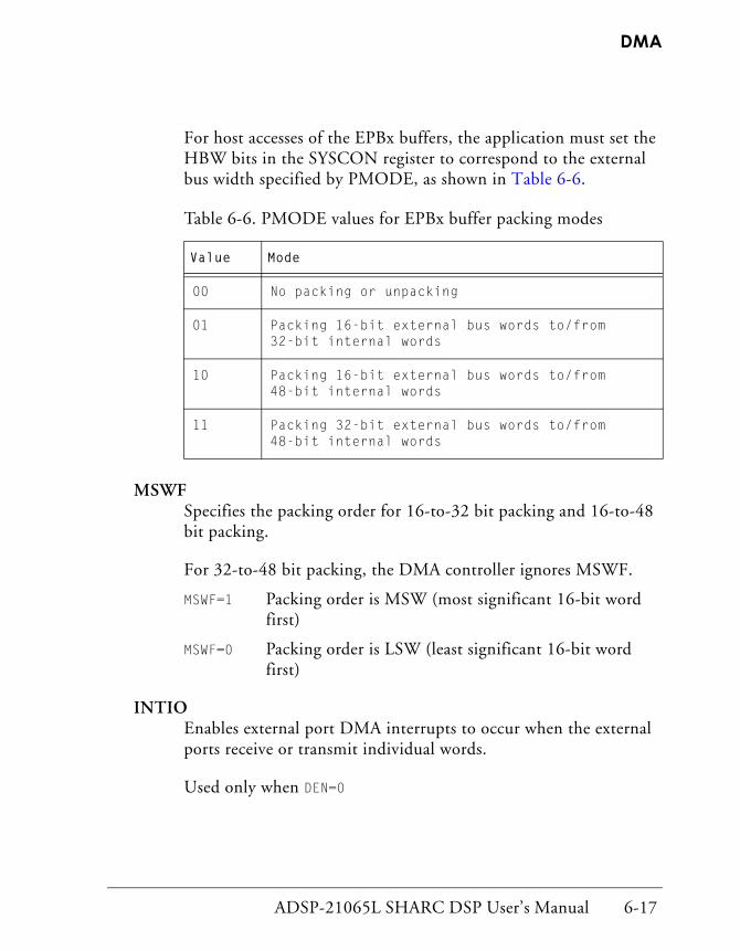
ADSP-21065L SHARC DSP User’s Manual 6-17
DMA
For host accesses of the EPBx buffers, the application must set the HBW bits in the SYSCON register to correspond to the external bus width specified by PMODE, as shown in Table 6-6.
MSWFSpecifies the packing order for 16-to-32 bit packing and 16-to-48 bit packing.
For 32-to-48 bit packing, the DMA controller ignores MSWF.
MSWF=1 Packing order is MSW (most significant 16-bit word first)
MSWF=0 Packing order is LSW (least significant 16-bit word first)
INTIOEnables external port DMA interrupts to occur when the external ports receive or transmit individual words.
Used only when DEN=0
Table 6-6. PMODE values for EPBx buffer packing modes
Value Mode
00 No packing or unpacking
01 Packing 16-bit external bus words to/from 32-bit internal words
10 Packing 16-bit external bus words to/from 48-bit internal words
11 Packing 32-bit external bus words to/from 48-bit internal words

DMA Control Registers
6-18 ADSP-21065L SHARC DSP User’s Manual
Generating DMA interrupts this way is useful for implementing interrupt-driven, single-word transfers that are under control of the processor’s core.
Setting INTIO=1 and:
TRAN=0 Causes the interrupts to occur when the EPBx input buffer is “not empty.”
TRAN=1 Causes the interrupts to occur when an output buffer is “not full.”
FLSH Reinitializes the state of the DMA channel, clearing the FS and PS status bits (setting them to 0).
This procedure flushes the external port FIFO buffer, the DMA request counter, and any partially packed data words. It also resets any internal DMA states. The entire procedure has a two-cycle latency.
FLSH is a self-clearing control bit, which is not latched and always reads as 0.
To avoid unexpected results, use the FLSH bit to clear the DMA channel only when the channel is inactive. To determine if the channel is active, read the DMASTAT register. (For any channel, the processor sets the channel active status bit in DMASTAT if DMA is enabled for the channel and the current DMA sequence is still in progress.)
Set the FLSH bit to 1 only when the DEN bit is 0 or at the same time you clear the DEN bit. Do not set FLSH to 1 in the same write that you set DEN to 1.
FS A two-bit status field that indicates whether data is present in the EPBx FIFO buffer.

ADSP-21065L SHARC DSP User’s Manual 6-19
DMA
When the processor is transmitting data to an external device, these status bits indicate whether the buffer has room for more data.
As shown in Table 6-7, when the processor is receiving data, these status bits indicate whether the buffer has new (unread) data.
MASTERMaster Mode DMA Enable.
The MASTER, HSHAKE, and EXTERN bits are used in combina-tion, as described Table 6-8.
HSHAKEDMA Handshake Mode Enable.
The MASTER, HSHAKE, and EXTERN bits are used in combina-tion, as described in Table 6-8.
EXTERNSpecifies an external memory to external device DMA transfer.
In this mode, HSHAKE must equal 1, and MASTER must equal 0.
Table 6-7. FS EPBx FIFO buffer status values
Value Status
00 Empty
01 Undefined
10 Partially full
11 Full
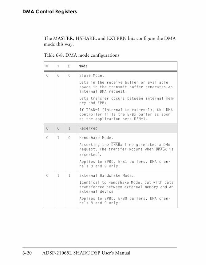
DMA Control Registers
6-20 ADSP-21065L SHARC DSP User’s Manual
The MASTER, HSHAKE, and EXTERN bits configure the DMA mode this way.
Table 6-8. DMA mode configurations
M H E Mode
0 0 0 Slave Mode.
Data in the receive buffer or available space in the transmit buffer generates an internal DMA request.
Data transfer occurs between internal mem-ory and EPBx.
If TRAN=1 (internal to external), the DMA controller fills the EPBx buffer as soon as the application sets DEN=1.
0 0 1 Reserved
0 1 0 Handshake Mode.
Asserting the DMARx line generates a DMA request. The transfer occurs when DMAGx is asserted*.
Applies to EPB0, EPB1 buffers, DMA chan-nels 8 and 9 only.
0 1 1 External Handshake Mode.
Identical to Handshake Mode, but with data transferred between external memory and an external device
Applies to EPB0, EPB0 buffers, DMA chan-nels 8 and 9 only.
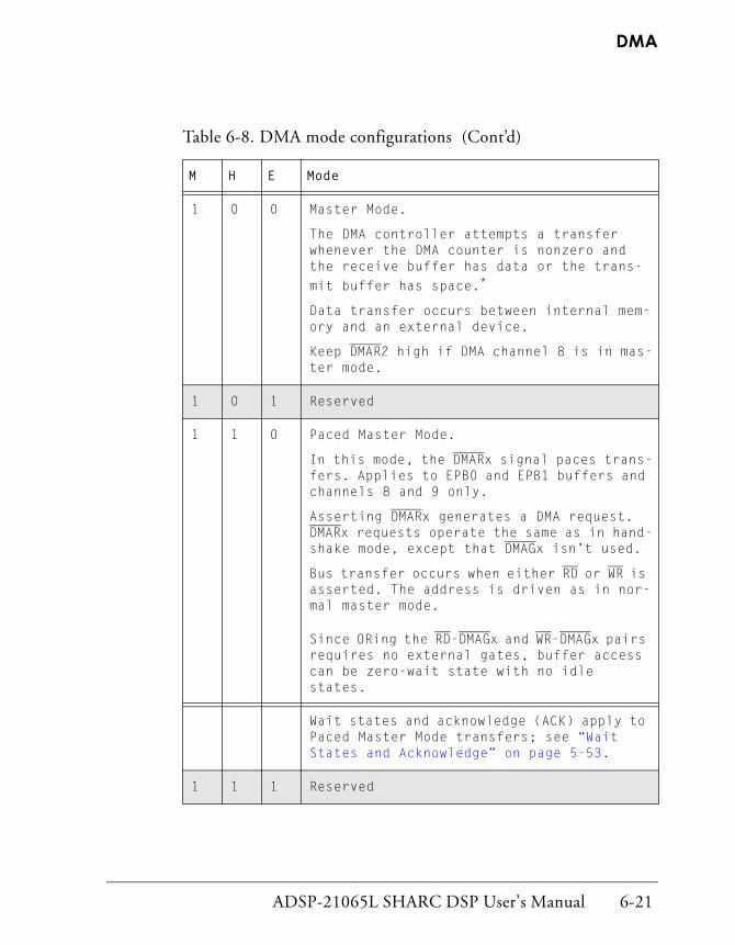
ADSP-21065L SHARC DSP User’s Manual 6-21
DMA
1 0 0 Master Mode.
The DMA controller attempts a transfer whenever the DMA counter is nonzero and the receive buffer has data or the trans-mit buffer has space.*
Data transfer occurs between internal mem-ory and an external device.
Keep DMAR2 high if DMA channel 8 is in mas-ter mode.
1 0 1 Reserved
1 1 0 Paced Master Mode.
In this mode, the DMARx signal paces trans-fers. Applies to EPB0 and EPB1 buffers and channels 8 and 9 only.
Asserting DMARx generates a DMA request. DMARx requests operate the same as in hand-shake mode, except that DMAGx isn’t used.
Bus transfer occurs when either RD or WR is asserted. The address is driven as in nor-mal master mode.
Since ORing the RD-DMAGx and WR-DMAGx pairs requires no external gates, buffer access can be zero-wait state with no idle states.
Wait states and acknowledge (ACK) apply to Paced Master Mode transfers; see “Wait States and Acknowledge” on page 5-53.
1 1 1 Reserved
Table 6-8. DMA mode configurations (Cont’d)
M H E Mode

DMA Control Registers
6-22 ADSP-21065L SHARC DSP User’s Manual
Serial Port DMA Control RegistersThe processor’s two serial ports, SPORT0 and SPORT1, can use DMA transfers to handle transmit and receive data. As shown in Table 6-9, DMA channels 0-7 are assigned to the serial ports.
The direction of SPORT DMA transfers is hardwired:
• Receive channels transfer data to internal memory.
• Transmit channels transfer data from internal memory.
The processor transmits 32-bit words internally between the RX and TX buffers and memory. Using the SPORTs’ packing capability, you can con-figure the processor to receive and transmit 16-bit serial words, two at a time. For details, see Chapter 10, Serial Ports.
Table 6-9. Serial port DMA channel assignments
DMA Chn
Data Buffer
Description
0 RX0_A Serial port 0; receive A data
1 RX0_B Serial port 0; receive B data
2 RX1_A Serial port 1; receive A data
3 RX1_B Serial port 1; receive B data
4 TX0_A Serial port 0; transmit A data
5 TX0_B Serial port 0; transmit B data
6 TX1_A Serial port 1; transmit A data
7 TX1_B Serial port 1; transmit B data
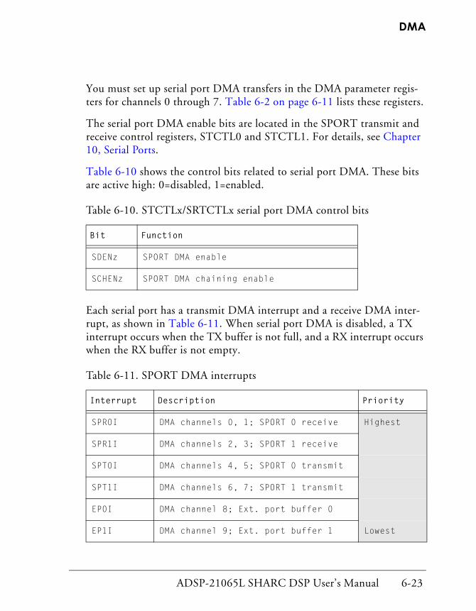
ADSP-21065L SHARC DSP User’s Manual 6-23
DMA
You must set up serial port DMA transfers in the DMA parameter regis-ters for channels 0 through 7. Table 6-2 on page 6-11 lists these registers.
The serial port DMA enable bits are located in the SPORT transmit and receive control registers, STCTL0 and STCTL1. For details, see Chapter 10, Serial Ports.
Table 6-10 shows the control bits related to serial port DMA. These bits are active high: 0=disabled, 1=enabled.
Each serial port has a transmit DMA interrupt and a receive DMA inter-rupt, as shown in Table 6-11. When serial port DMA is disabled, a TX interrupt occurs when the TX buffer is not full, and a RX interrupt occurs when the RX buffer is not empty.
Table 6-10. STCTLx/SRTCTLx serial port DMA control bits
Bit Function
SDENz SPORT DMA enable
SCHENz SPORT DMA chaining enable
Table 6-11. SPORT DMA interrupts
Interrupt Description Priority
SPR0I DMA channels 0, 1; SPORT 0 receive Highest
SPR1I DMA channels 2, 3; SPORT 1 receive
SPT0I DMA channels 4, 5; SPORT 0 transmit
SPT1I DMA channels 6, 7; SPORT 1 transmit
EP0I DMA channel 8; Ext. port buffer 0
EP1I DMA channel 9; Ext. port buffer 1 Lowest

DMA Control Registers
6-24 ADSP-21065L SHARC DSP User’s Manual
DMA Channel Status RegisterThe DMA controller maintains a 32-bit, read-only status register, DMASTAT, that provides information on the state of each of the proces-sor’s DMA channels.
Table 6-12 lists the bits and their definitions. Bits 0 through 9 indicate which DMA channels are active, with bit 0 corresponding to channel 0, and so on. Bits 10 through 19 indicate the DMA chaining status for each channel.
• Channel active status
1 = Active; transferring data or waiting to transfer the current block, not transferring TCB.
0 = Inactive; DMA disabled, transfer complete or transferring TCB.
• Channel chaining status
1 = Transferring TCB or waiting to transfer TCB.
Often, a DMA channel must wait to get control of the pro-cessor’s internal I/O bus before it can transfer the TCB. The length of the wait depends on the number of DMA channels active at the same time.
0 = Chaining disabled or not transferring TCB
Table 6-12. Bit definitions of the DMASTATx registers
Bit DMA Channel Status for…
0 0 Rx0_A
1 2 Rx1_A
2 4 Tx0_A

ADSP-21065L SHARC DSP User’s Manual 6-25
DMA
3 6 Tx1_A
4 1 Rx0_B
5 3 Rx1_B
6 8 EPB0
7 9 EPB1
8 5 Tx0_B
9 7 Tx1_B
10 0 Chaining on Rx0_A
11 2 Chaining on Rx1_A
12 4 Chaining on Tx0_A
13 6 Chaining on Tx1_A
14 1 Chaining on Rx0_B
15 3 Chaining on Rx1_B
16 8 Chaining on EPB0
17 9 Chaining on EPB1
18 5 Chaining on Tx0_B
19 7 Chaining on Tx1_B
20-31 Reserved
Table 6-12. Bit definitions of the DMASTATx registers (Cont’d)
Bit DMA Channel Status for…
DMA Control Registers
6-26 ADSP-21065L SHARC DSP User’s Manual
For a particular channel, the processor sets the channel active status bit if DMA is enabled and the current DMA transfer has not finished. It sets the chaining status bit if the channel is currently loading a TCB or if it is pre-paring to load a TCB. A single cycle of latency occurs between the time the processor changes the internal status and the time it updates the DMASTAT register.
As an alternative to interrupt-driven DMA, your application can poll DMASTAT to determine when a single DMA transfer has finished. To do so, the application reads DMASTAT to see if both status bits for the chan-nel are inactive. If so, the DMA sequence has finished.
Polling DMASTAT while the DMA controller is transferring data through an EPBx buffer may cause the processor to deassert its BRx line for one cycle. During this cycle, the host or another processor can take control of the bus, stalling the DMA transfer until the processor regains bus mastership.
Do not use polling if chaining is enabled because the next DMA sequence may have started by the time the processor returns the polled status.

ADSP-21065L SHARC DSP User’s Manual 6-27
DMA
DMA Controller OperationDMA controller operations occur over the internal I/O bus. The serial ports and external port connect to internal memory over the I/O Data bus (IOD), and the DMA controller generates internal memory addresses on the I/O Address bus (IOA).
The DMA controller maintains two DMA channels used by the external port and eight DMA channels used by the serial ports. Each DMA channel consists of a set of parameter registers that specify a data buffer in internal memory and hardware that an I/O port uses to request DMA service.
To transfer data, the DMA controller accepts internal requests from I/O ports and sends back an internal grant when it services the ports. The DMA controller contains priority logic that determines which channel can drive the bus in any given cycle. Because internal memory has separate ports for core and I/O accesses, DMA transfers never conflict with the core over access of internal memory.
Each external port DMA channel has a control and a status register (read-only) that set the channel’s operating mode and return its status information, respectively. External devices have access to all of the DMA control and parameter registers, which enables a host or other ADSP-21065L to set up a DMA channel and initiate transfers, without involving the local ADSP-21065L. To set up a DMA channel on itself, the processor writes to its own DMA control and parameter registers.
You can configure the external port DMA channels to transmit or receive data from internal memory, but since they are unidirectional, external port DMA channels either transmit or receive data only.
DMA Controller Operation
6-28 ADSP-21065L SHARC DSP User’s Manual
DMA Channel Parameter RegistersThe processor’s DMA channels and Data Address Generators (DAGs) operate similarly. Each channel has a set of parameter registers that includes an index register (IIyx_z), a modify register (IMyx_z), and a count register (Cyx_z). (For a complete list of these parameter registers, see Table 6-13 on page 6-31.) You use the index and modify registers to set up a data buffer in internal memory. You use the count register to determine when the processor generates an interrupt for the channel.
The application must initialize the index register with a starting address for the data buffer. The processor drives the address in the index register on its IOA (I/O Address) bus and applies it to internal memory during each DMA cycle. A DMA cycle is a clock cycle in which a DMA transfer is proceeding.
All addresses in the 17-bit index registers are offset by 0x0000 8000, the first internal RAM location, before the DMA controller uses them. The DMA controller cannot perform transfers to short word address space. (Using the processor's external port and serial port packing capability, however, you can transfer 16-bit short word data within 32-bit words.)
After transferring each data word to or from internal memory, the DMA controller adds the modify value to the index register to generate the address for the next DMA transfer. (It adds the modify value to the index value and writes the new value back to the index register.)
To enable both incrementing and decrementing, the modify value in the IM register is a signed integer. The modify value is fixed to 1 for DMA channels 0 through 7.
ADSP-21065L SHARC DSP User’s Manual 6-29
DMA
Each DMA channel has a count register (Cyx_z), which the application must initialize with the word count of the data to transfer. The count reg-ister decrements at the end of each DMA transfer. When the count register value reaches 0, the processor can generate an interrupt for the channel.
To start a new DMA sequence after the current one has finished:
1. Clear the DEN enable bit DMA interrupts.
2. Write new parameters to the II, IM, and C registers.
3. Set the DEN bit to re-enable DMA.
For chained DMA operations, this step is unnecessary.
If the index register (II) is modified past its maximum 17-bit value (the value falls outside the normal word address range of internal memory), the register wraps around to the beginning address of the particular block, where DMA transfers continue.
For block 0, the maximum bit value is x0000 9FFF, and the starting address is x0000 8000. For block 1, the maximum bit value is x0000 DFFF, and the starting address is x0000 C000. For details, see “Memory Organization” on page 5-16.
Initializing a channel’s count register with 0 does not disable DMA transfers on the channel. Instead, the channel performs
216 transfers because the first transfer starts before the controller tests the count value.
To disable a DMA channel, you clear the DMA enable bit in the channel’s control register.

DMA Controller Operation
6-30 ADSP-21065L SHARC DSP User’s Manual
Each DMA channel also has a chain pointer register (CPyx_z) and a gen-eral-purpose register (GPyx_z). You use the CP register to set up chained DMA operations and the GP register for any general purpose, such as stor-ing the address of the previously used buffer.
The external port DMA channels (EPBx) each contain three additional parameter registers:
• External index register (EIEPx)
• External modify register (EMEPx)
• External count register (ECEPx)
(Serial port DMA channels do not have these registers.)
You use the EIEP, EMEP, and ECEP registers to generate 32-bit addresses that are driven out of the external port for master mode DMA transfers between internal memory and external memory or devices.
The MASTER bit of each DMACx control register configures Master Mode. In Master Mode only, you must load the ECEP register with the number of external bus transfers to perform. (This count differs from the number of words the DMA controller transfers when you use word pack-ing.) EIEPx cannot index internal memory.
If the index register (EIEPx) is modified past its maximum 32-bit value (the value falls outside the external memory bank address range of internal memory), the processor continues to drive the ADDRx, RD, WR, and DATAx lines, but it does not drive any of the MSx lines. So, when the index register over-flows, the processor gives no indication that it has, and no mem-ory reads or writes occur.
You can use the upper bits of ADDRx to generate addresses out-side the external memory bank address range.
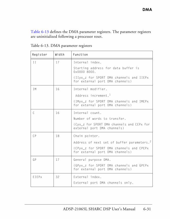
ADSP-21065L SHARC DSP User’s Manual 6-31
DMA
Table 6-13 defines the DMA parameter registers. The parameter registers are uninitialized following a processor reset.
Table 6-13. DMA parameter registers
Register Width Function
II 17 Internal index.
Starting address for data buffer is 0x0000 8000.
(IIyx_z for SPORT DMA channels and IIEPx for external port DMA channels)
IM 16 Internal modifier.
Address increment.1
(IMyx_z for SPORT DMA channels and IMEPx for external port DMA channels)
C 16 Internal count.
Number of words to transfer.
(Cyx_z for SPORT DMA channels and CEPx for external port DMA channels)
CP 18 Chain pointer.
Address of next set of buffer parameters.2
(CPyx_z for SPORT DMA channels and CPEPx for external port DMA channels)
GP 17 General purpose DMA.
(GPyx_z for SPORT DMA channels and GPEPx for external port DMA channels)
EIEPx 32 External index.
External port DMA channels only.

DMA Controller Operation
6-32 ADSP-21065L SHARC DSP User’s Manual
Table 6-14 lists the parameter registers for each DMA channel.
EMEPx 32 External modifier.
External port DMA channels only.
ECEPx 32 External count.
External port DMA channels only.
1 The modify value of DMA channels 0-7 is fixed to 1.2 Lower 17 bits (bits 16-0) contain the memory address of the next set of parameters for chained
DMA operations. Most significant bit (bit 17) is the PCI bit (Program-Controlled Interrupts), which determines whether the DMA interrupts occur at the completion of each DMA sequence.
Table 6-14. Parameter registers of each DMA channel
DMA Chn Registers Description
0 IIR0A, IMR0A1, CR0A, CPR0A, GPR0A
SPORT 0 receive; A data
1 IIR0B, IMR0B, CR0B, CPR0B, GPR0B
SPORT 0 receive; B data
2 IIR1A, IMR1A, CR1A, CPR1A, GPR0A
SPORT 1 receive; A data
3 IIR1B, IMR1B, CR1B, CPR1B, GPR1B
SPORT 1 receive; B data
4 IIT0A, IMT0A, CT0A, CTR0A, GPT0A
SPORT0 Transmit; A data
5 IIT0B, IMT0B, CT0B, CPT0B, GPT0B
SPORT0 Transmit; B data
Table 6-13. DMA parameter registers (Cont’d)
Register Width Function

ADSP-21065L SHARC DSP User’s Manual 6-33
DMA
Figure 6-4 on page 6-34 shows a block diagram of the DMA controller’s address generator.
6 IIT1A, IMT1A, CT1A, CTR1A, GPT1A
SPORT 1 Transmit; A data
7 IIT1B, IMT1B, CT1B, CPT1B, GPT1B
SPORT 1 Transmit; B data
8 IIEP0, IMEP0, CEP0, CPEP0, GPEP0, EIEP0, EMEP0, ECEP0
External Port Buffer 0
9 IIEP1, IMEP1, CEP1, CPEP1, GPEP1, EIEP1, EMEP1, ECEP1
External Port Buffer 1
1 The values in the IMyx_z registers are fixed to 1.
Table 6-14. Parameter registers of each DMA channel (Cont’d)
DMA Chn Registers Description

DMA Controller Operation
6-34 ADSP-21065L SHARC DSP User’s Manual
Figure 6-4. DMA address generation
DMA Word Counter
CxCount
CPxChain Pointer
MUX
+
Local Bus
GPxGeneral Purpose
working register−1
IIxIndex (Address)
IMxModifier
MUX+
Local Bus
InternalMemoryAddress
Postmodify
DMA Address Generator
DMA Address Generator(External Memory)
For External Port DMA Channels Only
EIxExt. Index (Addr)
EMxExt. Modifier
+
Local Bus
ExternalMemoryAddress
Postmodify
ECxExt. Count
+−1
ADSP-21065L SHARC DSP User’s Manual 6-35
DMA
Internal Request and GrantThe processor’s I/O ports use internal DMA request and grant handshake hardware and protocol to communicate with the DMA controller.
Each serial port and external port DMA channel has one request and one grant line. When an I/O port needs to write data to internal memory, it asserts its request line. The DMA controller prioritizes this request with all other valid DMA requests. See Figure 6-2 on page 6-3.
When a channel’s request takes highest priority, the DMA controller asserts that channel’s internal grant line and starts the transfer in the next cycle. The DMA controller follows the same sequence when an I/O port requests read data from internal memory.
If a DMA channel is disabled, the DMA controller does not assert the channel’s grant line, even if the channel has data to transfer.
Setting DMA Channel PrioritizationSince more than one DMA channel can have a request active in any cycle, the DMA controller uses a prioritization scheme to select which channel to service.
Prioritization enables the DMA controller to determine which channel can use the IOD bus to access memory. Except for the external port DMA channels, the processor always uses a fixed prioritization scheme. For external port DMA prioritization, see Table 6-15 on page 6-36, which lists, in descending order, the prioritization of I/O bus accesses, including DMA channels.
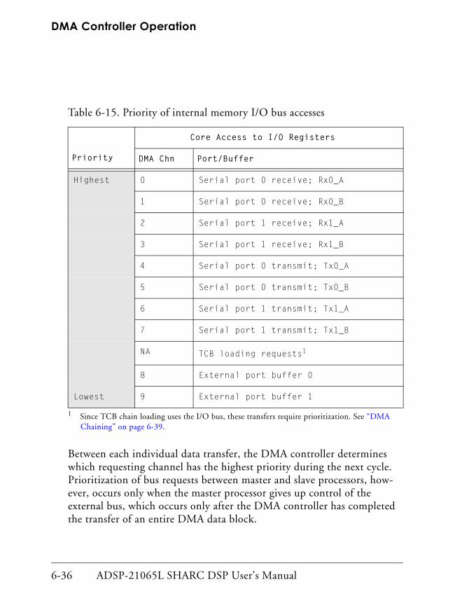
DMA Controller Operation
6-36 ADSP-21065L SHARC DSP User’s Manual
Between each individual data transfer, the DMA controller determines which requesting channel has the highest priority during the next cycle. Prioritization of bus requests between master and slave processors, how-ever, occurs only when the master processor gives up control of the external bus, which occurs only after the DMA controller has completed the transfer of an entire DMA data block.
Table 6-15. Priority of internal memory I/O bus accesses
Priority
Core Access to I/O Registers
DMA Chn Port/Buffer
Highest 0 Serial port 0 receive; Rx0_A
1 Serial port 0 receive; Rx0_B
2 Serial port 1 receive; Rx1_A
3 Serial port 1 receive; Rx1_B
4 Serial port 0 transmit; Tx0_A
5 Serial port 0 transmit; Tx0_B
6 Serial port 1 transmit; Tx1_A
7 Serial port 1 transmit; Tx1_B
NA TCB loading requests1
1 Since TCB chain loading uses the I/O bus, these transfers require prioritization. See “DMA Chaining” on page 6-39.
8 External port buffer 0
Lowest 9 External port buffer 1
ADSP-21065L SHARC DSP User’s Manual 6-37
DMA
Rotating Priority for External Port Channels
You can program the DMA controller to use a rotating priority scheme for the two external port channels. To do so, you set the DCPR bit in the SYSCON register.
The DCPR bit enables rotating priority for external port DMA channels 8 and 9.
DCPR = 0 disable
DCPR = 1 enable
When rotating priority is enabled, high priority shifts back and forth between DMA channels 8 and 9 after each single-word transfer.
For example, rotation proceeds this way:
1. After reset, the default priority ordering, from high to low, is chan-nel 8 to channel 9.
2. A single transfer is performed on channel 8.
The processor prioritizes external direct accesses of internal memory and TCB chain loading with the DMA channels.
It does so to prevent contention over the internal I/O bus since these accesses occur over it. TCB chain loading has higher prior-ity than external port accesses to enable chaining of serial port DMA transfers, which cannot be held off, even when the exter-nal port is attempting an access in every cycle. (For details, see “Transfer Control Blocks and Chain Loading” on page 6-41.)

DMA Controller Operation
6-38 ADSP-21065L SHARC DSP User’s Manual
3. With rotating priority enabled (DCPR=1), priority shifts to channel 9.
The external port channel priorities do not change relative to the serial port channel priorities. At reset, the processor clears the DCPR bit, disabling rotating priority.
When using fixed priority for the external port DMA channels, the high-est priority is assigned to channel 8, and the lowest priority is assigned to channel 9. To redefine this priority, you assign channel 9 the highest priority.
To do so:
1. Disable external port DMA channel 8 only.
2. Select rotating priority, set DCPR = 1.
3. Generate at least one transfer on channel 9.
4. Disable rotating priority (DCPR = 0), and re-enable both external port DMA channels.
Table 6-16 illustrates this procedure.
Table 6-16. Example changing priority assignment
Priority @… Highest Lowest
Reset DMA 8 DMA 9
Follow steps 1-4 above to make DMA 8 lowest priority.
Reorder DMA 9 DMA 8

ADSP-21065L SHARC DSP User’s Manual 6-39
DMA
DMA ChainingDMA chaining enables the processor’s DMA controller to autoinitialize itself between multiple DMA transfers. Using chaining, you can set up multiple DMA operations in which each operation has different attributes.
In chained DMA operations, the processor automatically sets up another DMA transfer when its DMA controller has transmitted or received the entire contents of the current buffer. The processor supports DMA chain-ing on the same channel only. It does not support cross-channel chaining.
You use the chain pointer register (CP) to point to the next set of DMA parameters stored in internal memory. This new set of parameters is called a transfer control block (TCB). To set up the next DMA sequence, the pro-cessor’s DMA controller automatically reads the TCB from internal memory and loads the parameter values into the channel parameter regis-ters. This procedure is called TCB chain loading.
A DMA sequence is the sum of the DMA transfers for a single channel, starting with the initialization of the parameter registers and ending with the point at which the decrementing count register reaches zero (0).
Each DMA channel has a chaining enable bit (CHEN) in its correspond-ing control register. To enable chaining, you set this bit to 1, and to disable chaining, you write all zeros (0s) to the address field of the chain pointer register (CP).
With chaining enabled, to initiate DMA transfers, you write a memory address to the CP register. This is also an easy way to start a single DMA sequence, which includes no subsequent chained DMA transfers. Since you can load the CP register any time during the DMA sequence, you can disable chaining on a DMA channel (CP register address field = 0x0000) until an event occurs that loads the CP register with a non-zero value.
The lower seventeen bits of the 18-bit wide CP register is the memory address field, which is offset by 0x0000 8000 before the DMA controller

DMA Controller Operation
6-40 ADSP-21065L SHARC DSP User’s Manual
uses it. Bit 17, the PCI (Program-Controlled Interrupts) bit, is a control bit and the most significant bit of the CP register.
Used in conjunction with the interrupt’s mask bit in IMASK, the PCI bit selects whether or not an interrupt occurs at the completion of the current DMA sequence, but only on DMA channels with chaining enabled (CHEN=1).
PCI=1 Enables the corresponding DMA channel interrupt, which occurs when the count register reaches 0.
PCI=0 Disables the DMA channel’s interrupt.
For nonchained DMA operations, you must use the IMASK register to disable the interrupt. But you can still mask out (disable), in the IMASK register, interrupt requests enabled by the PCI bit. Figure 6-5 shows the CP register and PCI bit.
Figure 6-5. Chain pointer register and PCI bit
Because the PCI bit is not part of the memory address in the CP register, take care when writing and reading addresses to and from the register. To prevent errors, mask out the PCI bit (bit 17) when you copy the address in CP to another address regis-ter.
17 16 15 14 13 12 11 10 9 8 7 6 5 4 3 2 1 0
PCI bit Memory Address field(Address of next TCB)

ADSP-21065L SHARC DSP User’s Manual 6-41
DMA
The processor loads the general-purpose (GP) register from memory with the other parameter registers. You can use it during chained DMA sequences to point to the last DMA sequence that the DMA controller finished transferring. This procedure enables an application to determine the location of the last full (or empty) data buffer. Since a general-purpose register has no dedicated functionality, you can use it for any purpose.
Transfer Control Blocks and Chain Loading
During TCB chain loading, the processor loads the DMA channel param-eter registers with values retrieved from internal memory. The CP register contains the chain pointer, which is the highest address of the TCB. The TCB is stored in consecutive locations.
Table 6-17 shows the TCB-to-register loading sequence for the external port and serial port DMA channels. The loading sequence is the order in which the DMA controller reads and loads each word of the TCB into its corresponding register.
Figure 6-6 on page 6-43 shows how to set up in memory the TCB for an external port DMA chain, which is referenced to the address pointer con-tained in the CP register of the previous DMA operation in the chain.
Table 6-17. TCB chain loading sequence
Address + Offset Ext. Port Buffers
Serial Ports
CPyx_z + 0x0000 8000 IIEPx IIyx_z
CPyx_z - 1 + 0x0000 8000 IMEPx IMyx_z
CPyx_z - 2 + 0x0000 8000 CEPx Cyx_z
CPyx_z - 3 + 0x0000 8000 CPEPx CPyx_z

DMA Controller Operation
6-42 ADSP-21065L SHARC DSP User’s Manual
TCB chain loading is requested the same way as all other DMA opera-tions. The processor latches and holds a TCB loading request in the DMA controller until the TCB becomes the request with highest priority. As in normal DMA operation, the I/O Processor prioritizes and transfers the TCB registers individually. If multiple chaining requests are present, the DMA controller transfers the TCB registers for the highest priority DMA channel first. A channel with higher priority cannot interrupt a channel that is currently chain loading. See Table 6-15 on page 6-36 for DMA channel request priorities.
CPyx_z - 4 + 0x0000 8000 GPEPx GPyx_z
CPyx_z - 5 + 0x0000 8000 EIEPx
CPyx_z - 6 + 0x0000 8000 EMEPx
CPyx_z - 7 + 0x0000 8000 ECEPx
CPyx_z - 8 + 0x0000 8000 —
Table 6-17. TCB chain loading sequence (Cont’d)
Address + Offset Ext. Port Buffers
Serial Ports

ADSP-21065L SHARC DSP User’s Manual 6-43
DMA
Figure 6-6. TCB memory setup for external port DMA channels
Setting Up and Starting a Chain
To setup and initiate a chain of DMA transfers:
1. Set up all TCBs in internal memory.
2. Write to the appropriate DMA control register, and set DEN=1 and CHEN=1.
3. To start the chain, write to the channel’s CP register the last address (the address of the II register value) of the first TCB.
Before starting the first transfer, the DMA controller autoinitializes itself with the first TCB. On completion of this transfer, the DMA controller starts the next transfer if the current chain pointer address is nonzero. The DMA controller uses this address as the pointer to the next TCB.
ECx
EMx
EIx
GPx
CPx
Cx
IMx
IIx
Address
CPx −7
CPx −6
CPx −5
CPx −4
CPx −3
CPx −2
CPx −1
CPx
Address pointerto next TCB
Lowest address
Highest address
DMA Controller Operation
6-44 ADSP-21065L SHARC DSP User’s Manual
Inserting a ChainYou can insert a high priority DMA operation or chain into an active DMA chain.
Setting CHEN=1 and DEN=0 places the DMA channel in chain insertion mode. In this mode, a new DMA chain inserted into the current chain does not affect the current DMA operation. The processor’s core writes a TCB into the channel parameter registers to insert the new chain.
In this mode, the DMA channel operates normally (as with CHEN=1 and DEN=1), except that at the end of the current DMA transfer, automatic chaining is disabled, and an interrupt request occurs. This interrupt request is independent of the PCI bit state.
Use this sequence to insert a DMA subchain while another chain is active:
1. To enter chain insertion mode, set CHEN=1 and DEN=0 in the appro-priate DMA control register.
The DMA interrupt occurs to indicate when the current DMA sequence has finished.
2. Write the CP register value into the CP position of the last TCB in the new chain.
The address field of the CP registers is only seventeen bits wide. A symbolic address written directly to the CP register can cause a conflict between bit 17 and the PCI bit. Be sure to clear the upper bits of the address first, before you AND in the PCI bit separately (if necessary).
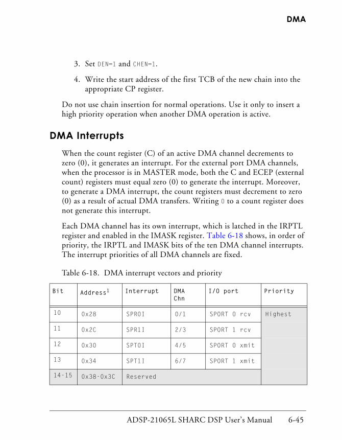
ADSP-21065L SHARC DSP User’s Manual 6-45
DMA
3. Set DEN=1 and CHEN=1.
4. Write the start address of the first TCB of the new chain into the appropriate CP register.
Do not use chain insertion for normal operations. Use it only to insert a high priority operation when another DMA operation is active.
DMA InterruptsWhen the count register (C) of an active DMA channel decrements to zero (0), it generates an interrupt. For the external port DMA channels, when the processor is in MASTER mode, both the C and ECEP (external count) registers must equal zero (0) to generate the interrupt. Moreover, to generate a DMA interrupt, the count registers must decrement to zero (0) as a result of actual DMA transfers. Writing 0 to a count register does not generate this interrupt.
Each DMA channel has its own interrupt, which is latched in the IRPTL register and enabled in the IMASK register. Table 6-18 shows, in order of priority, the IRPTL and IMASK bits of the ten DMA channel interrupts. The interrupt priorities of all DMA channels are fixed.
Table 6-18. DMA interrupt vectors and priority
Bit Address1 Interrupt DMA Chn
I/O port Priority
10 0x28 SPR0I 0/1 SPORT 0 rcv Highest
11 0x2C SPR1I 2/3 SPORT 1 rcv
12 0x30 SPT0I 4/5 SPORT 0 xmit
13 0x34 SPT1I 6/7 SPORT 1 xmit
14-15 0x38-0x3C Reserved

DMA Controller Operation
6-46 ADSP-21065L SHARC DSP User’s Manual
When DMA chaining is enabled, you can use the PCI bit in the CP regis-ter, instead of IMASK, to enable and disable DMA interrupts for each channel configured for chaining.
PCI=1 DMA interrupt requests occur when the count register reaches zero (0).
PCI=0 DMA interrupts disabled.
The PCI bit is valid only when DMA chaining is enabled. If chaining is disabled, you must use the IMASK register to disable interrupts. You can still mask out (disable) interrupt requests enabled by PCI in the IMASK register.
The processor’s I/O ports can generate DMA interrupts without using DMA. In this case, two conditions generate an interrupt:
• The receive buffer contains data.
• The transmit buffer has space.
Generating DMA interrupts this way is useful for implementing inter-rupt-driven I/O controlled by the processor’s core. Multiple interrupts can occur if several I/O ports transmit or receive data in the same cycle. To perform single-word, non-DMA interrupt-driven transfers on the external port, you must set the INTIO bit in the appropriate DMACx control register.
16 0x40 EP0I 8 EPB0
17 0x44 EP1I 9 EPB1 Lowest
1 Offset from base address: 0x0000 8000 for interrupt vector table in internal memory, 0x0002 0000 for interrupt vector table in external memory.
Table 6-18. DMA interrupt vectors and priority (Cont’d)
Bit Address1 Interrupt DMA Chn
I/O port Priority
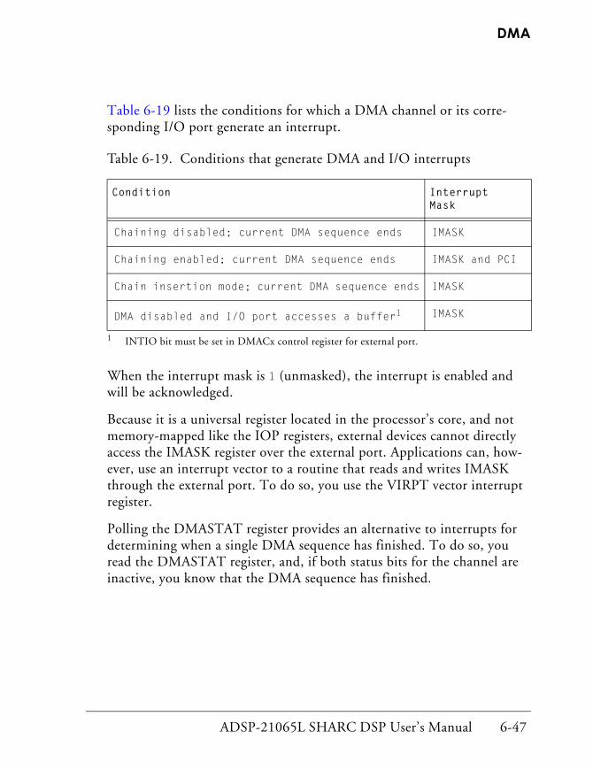
ADSP-21065L SHARC DSP User’s Manual 6-47
DMA
Table 6-19 lists the conditions for which a DMA channel or its corre-sponding I/O port generate an interrupt.
When the interrupt mask is 1 (unmasked), the interrupt is enabled and will be acknowledged.
Because it is a universal register located in the processor’s core, and not memory-mapped like the IOP registers, external devices cannot directly access the IMASK register over the external port. Applications can, how-ever, use an interrupt vector to a routine that reads and writes IMASK through the external port. To do so, you use the VIRPT vector interrupt register.
Polling the DMASTAT register provides an alternative to interrupts for determining when a single DMA sequence has finished. To do so, you read the DMASTAT register, and, if both status bits for the channel are inactive, you know that the DMA sequence has finished.
Table 6-19. Conditions that generate DMA and I/O interrupts
Condition Interrupt Mask
Chaining disabled; current DMA sequence ends IMASK
Chaining enabled; current DMA sequence ends IMASK and PCI
Chain insertion mode; current DMA sequence ends IMASK
DMA disabled and I/O port accesses a buffer1
1 INTIO bit must be set in DMACx control register for external port.
IMASK
DMA Controller Operation
6-48 ADSP-21065L SHARC DSP User’s Manual
Starting and Stopping DMA SequencesThe way DMA sequences start depends on whether DMA chaining is enabled. When chaining is disabled, only the DMA enable bit (DEN) enables or disables DMA transfers.
A DMA sequence starts when one of the following occurs:
• Chaining is disabled, and the DMA enable bit (DEN) transitions from low to high.
• Chaining is enabled, DMA is enabled (DEN=1), and the application writes a nonzero value to the CP register address field.
In this case, TCB chain loading of the channel parameter registers occurs first.
• Chaining is enabled, the CP register address field is nonzero, and the current DMA sequence finishes.
In this case, TCB chain loading occurs.
Polling DMASTAT while the DMA controller is transferring data through an EPBx buffer may cause the processor to deassert its BRx line for one cycle. During this cycle, the host or another processor can take control of the bus, stalling the DMA transfer until the processor regains bus mastership.
Do not use polling if chaining is enabled because the next DMA sequence may have started by the time the processor returns the polled status.

ADSP-21065L SHARC DSP User’s Manual 6-49
DMA
A DMA sequence ends when one of the following occurs:
• The count register decrements to 0 (for external port channels, both C and ECEP).
• Chaining is disabled, and the channel’s DEN bit transitions from high to low.
If the DEN bit goes low and chaining is enabled, the channel enters chain insertion mode, and the DMA sequence continues. (For details, see “Inserting a Chain” on page 6-44.)
To start a new DMA sequence after the current one has finished:
1. Clear the DEN bit.
2. Write new parameters to the II, IM, and C registers.
3. Set the DEN bit to re-enable DMA.
(For chained DMA operations, however, this is not necessary. See “DMA Chaining” on page 6-39.)
When the DEN bit goes high again, the DMA sequence continues from where it stopped (for nonchained opera-tions only).

External Port DMA
6-50 ADSP-21065L SHARC DSP User’s Manual
External Port DMAChannels 8 and 9 are the external port DMA channels.
These DMA channels enable efficient data transfers between the proces-sor’s internal memory and external memory or devices. DMA transfers between the processor and any external device that lacks bus master capa-bility use these channels.
External Port FIFO Buffers (EPBx)DMA Channels 8 and 9 are associated with the external port FIFO data buffers, EPB0 and EPB1.
Each buffer acts as a six-location FIFO, and each has two ports—a read port and a write port. Each port can connect to either the EPD (External Port Data) bus or to the IOD (I/O Data) bus, the PM Data bus, or the DM Data bus. (See Figure 6-2 on page 6-3.)
The FIFO structure enables DMA transfers at full processor clock fre-quency since reads and writes of the same data can occur at the same time through the FIFO’s separate read and write ports.
You can use the external port FIFO buffers for non-DMA, single-word data transfers too. For details, see Chapter 8‚ Host Interface.
To flush (clear) an external port buffer, write 1 to the FLSH bit in the appropriate DMACx control register. Do so only when DMA for the channel is disabled.
Do not attempt core reads or writes of an EPBx buffer when a DMA operation using that buffer is in progress. Doing so cor-rupts the DMA data.

ADSP-21065L SHARC DSP User’s Manual 6-51
DMA
The FLSH bit is not latched internally and always reads as 0. Status can change in the following cycle.
Do not enable and flush an external port buffer in the same cycle.
External Port DMA Data Packing
Each external port buffer contains data packing logic to pack 8-, 16-, or 32-bit external bus words into 32- or 48-bit internal words. The packing logic is reversible to unpack 32-bit or 48-bit internal data into 8-, 16-, or 32-bit external data.
The PMODE bits in the DMACx control registers determine the packing mode for internal bus words, and the HBW bits in the SYSCON register determine the packing mode for external bus words. The type of access, host or processor-to-processor or processor-to-memory, determines which packing bits you need to set to select a packing mode.
For processor accesses of another ADSP-21065L or of memory while using master mode, paced master mode, or handshake mode DMA, to pack and unpack individual data words, you must set the PMODE bits only (HBW bits have no effect), as shown in Table 6-20.
Table 6-20. PMODE values for EPBx buffer packing modes
Value Mode
00 No packing or unpacking
01 Packing 16-bit external bus words to/from 32-bit internal words
10 Packing 16-bit external bus words to/from 48-bit internal words
11 Packing 32-bit external bus words to/from 48-bit internal words

External Port DMA
6-52 ADSP-21065L SHARC DSP User’s Manual
For host accesses, to pack and unpack individual data words, you must set both the PMODE bits in the appropriate DMACx control register and the HBW bits in the SYSCON register, as shown in Table 6-21.
The external port buffer can pack data in most significant word first (MSWF) order or in least significant word first (LSWF) order. Setting the MSWF bit to 1 in the DMACx control register selects MSW mode for both packing and unpacking operations. The MSWF bit has no effect when PMODE=11 or PMODE=00.
The packing sequence for downloading processor instructions from a 32-bit bus (PMODE=11, HBW=00) takes three cycles for every two words, as Table 6-22 shows.
Table 6-21. Packing modes using PMODE and HBW bits
DMA Packing Mode Host Bus Width
PMODE Internal bits 00 (32b) 01 (16b) 10 (8b)
00 Invalid for host DMA transfers through the EPBx buffers. Valid only for nonhost-based DMA transfers.
01 32 No pack 16 ↔ 32 8 ↔ 32
10 48 32 ↔ 48 16 ↔ 48 8 ↔ 48
11 Identical to PMODE = 10
Table 6-22. Packing sequence for downloading instructions from a 32-bit bus
Transfer Data bus lines 31-16 Data Bus Lines 15-0
First Word 1; bits 47-32 Word 1; bits 31-16
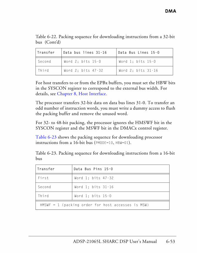
ADSP-21065L SHARC DSP User’s Manual 6-53
DMA
For host transfers to or from the EPBx buffers, you must set the HBW bits in the SYSCON register to correspond to the external bus width. For details, see Chapter 8‚ Host Interface.
The processor transfers 32-bit data on data bus lines 31-0. To transfer an odd number of instruction words, you must write a dummy access to flush the packing buffer and remove the unused word.
For 32- to 48-bit packing, the processor ignores the HMSWF bit in the SYSCON register and the MSWF bit in the DMACx control register.
Table 6-23 shows the packing sequence for downloading processor instructions from a 16-bit bus (PMODE=10, HBW=01).
Second Word 2; bits 15-0 Word 1; bits 15-0
Third Word 2; bits 47-32 Word 2; bits 31-16
Table 6-23. Packing sequence for downloading instructions from a 16-bit bus
Transfer Data Bus Pins 15–0
First Word 1; bits 47-32
Second Word 1; bits 31-16
Third Word 1; bits 15-0
HMSWF = 1 (packing order for host accesses is MSW)
Table 6-22. Packing sequence for downloading instructions from a 32-bit bus (Cont’d)
Transfer Data bus lines 31-16 Data Bus Lines 15-0

External Port DMA
6-54 ADSP-21065L SHARC DSP User’s Manual
The HMSWF bit determines whether the I/O processor packs the most significant 16-bit word or the least significant 16-bit word first. See Chap-ter 5, Memory, for details on allocating memory for different word widths.
The packing sequence for downloading processor instructions from an 8-bit bus (PMODE=10, HBW=10) takes six cycles for each word, as Table 6-24 shows.
The HMSWF bit in SYSCON determines whether the I/O processor packs the most significant or least significant 8-bit word first.
Packing Status
Each external port DMA control register contains a 2-bit PS field, which indicates the number of short words currently packed in the EPBx buffer. The PS status field behaves the same way during packing and unpacking operations. All packing functions are available for all types of DMA transfer.
Table 6-24. Host to processor, 8- to 48-bit word packing
Transfer Data Bus Pins 7-0
First Word 1; bits 47-40
Second Word 1; bits 39-32
Third Word 1; bits 31-24
Fourth Word 1; bits 23-16
Fifth Word 1; bits 15-8
Sixth Word 1; bits7-0
HMSWF = 1 (packing order for host accesses is MSW)

ADSP-21065L SHARC DSP User’s Manual 6-55
DMA
Generating Internal and External AddressesFor DMA transfers between the processor’s internal memory and external memory, the DMA controller must generate addresses in both memories. The external port DMA channels contain both EIEP (External Index) and EMEP (External Modifier) registers to generate external addresses. The EIEP register provides the external port address for the current DMA cycle, and it is updated with the modifier value in EMEP for the next external memory access.
To support the wide range of data packing options provided for external DMA transfers, the EIEP and EMEP registers can generate addresses at a different rate than the internal address generating registers IIEP and IMEP. For this reason, the internal and external address generators oper-ate independently, and the ECEP (External Count) register serves as the external DMA word counter.
When, for example, a 16-bit DMA device reads data from the processor’s internal memory, two external 16-bit transfers occur for each 32-bit inter-nal memory word, and the ECEP (external) word count is twice the value of the CEP (internal) word count.
External Port DMA ModesThe MASTER, HSHAKE, and EXTERN bits of each DMACx control register select the DMA operation mode for the channel. You can set up each external port DMA channel to operate in one of five DMA modes as shown in Table 6-25 on page 6-56.
Only master mode initiates transfers, and all other modes act as slave, requiring an external device to initiate each transfer.

External Port DMA
6-56 ADSP-21065L SHARC DSP User’s Manual
Table 6-25 shows how the MASTER, HSHAKE, and EXTERN bits in combination configure the DMA mode.
Table 6-25. DMACx register DMA mode configuration bit combinations
M H E Mode1
0 0 0 Slave Mode.
The DMA controller generates a DMA request whenever an Rx buffer is not empty or a Tx buffer is not full.2
0 0 1 Reserved.
0 1 0 Handshake Mode.
Applies to the EPBx buffers (channels 8 and 9) only.
The DMA controller generates a DMA request when the DMARx line is asserted and begins transferring the data when the processor asserts the DMAGx line.
0 1 1 External Handshake Mode.
Applies to the EPBx buffers (channels 8 and 9) only.
Identical to Handshake Mode, except the DMA con-troller transfers the data between external memory and an external device.
The processor does not support this mode on an external memory bank mapped to SDRAM.
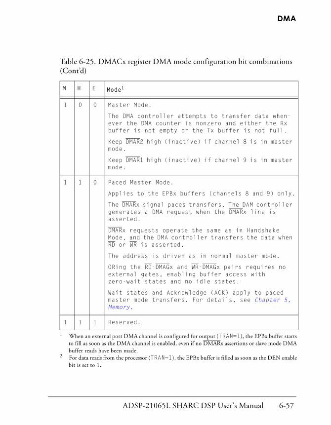
ADSP-21065L SHARC DSP User’s Manual 6-57
DMA
1 0 0 Master Mode.
The DMA controller attempts to transfer data when-ever the DMA counter is nonzero and either the Rx buffer is not empty or the Tx buffer is not full.
Keep DMAR2 high (inactive) if channel 8 is in master mode.
Keep DMAR1 high (inactive) if channel 9 is in master mode.
1 1 0 Paced Master Mode.
Applies to the EPBx buffers (channels 8 and 9) only.
The DMARx signal paces transfers. The DAM controller generates a DMA request when the DMARx line is asserted.
DMARx requests operate the same as in Handshake Mode, and the DMA controller transfers the data when RD or WR is asserted.
The address is driven as in normal master mode.
ORing the RD-DMAGx and WR-DMAGx pairs requires no external gates, enabling buffer access with zero-wait states and no idle states.
Wait states and Acknowledge (ACK) apply to paced master mode transfers. For details, see Chapter 5, Memory.
1 1 1 Reserved.
1 When an external port DMA channel is configured for output (TRAN=1), the EPBx buffer starts to fill as soon as the DMA channel is enabled, even if no DMARx assertions or slave mode DMA buffer reads have been made.
2 For data reads from the processor (TRAN=1), the EPBx buffer is filled as soon as the DEN enable bit is set to 1.
Table 6-25. DMACx register DMA mode configuration bit combinations (Cont’d)
M H E Mode1

External Port DMA
6-58 ADSP-21065L SHARC DSP User’s Manual
Master Mode
For a channel configured for master mode, the DMA controller generates internal DMA requests for the channel until the DMA sequence has finished.
While in master mode, the processor drives the external bus control signals.
Setting DMACx bits,
MASTER=1
HANDSHAKE=0
EXTERN=0
places the corresponding DMA channel in master mode. You can specify master mode independently for each external port DMA channel.
Examples of DMA master mode operations include:
• Transfers between internal memory and external memory.
• Transfers from internal memory to external devices.
In both cases, the data is set up in memory, so the processor can run the complete sequence without having to interact with other devices.
Paced Master Mode
In paced master mode, DMARx requests operate the same way as in hand-shake mode, but DMAGx is inactive. The slave processor asserts DMARx to initiate each transfer.
Serial port DMA channels do not have the MASTER control bit and do not operate in master mode.
ADSP-21065L SHARC DSP User’s Manual 6-59
DMA
The processor responds to requests with the RD or WR strobe only. This method enables both the DMA controller and core I/O to share the same buffer without external gating.
To extend paced master mode accesses, you can:
• Use the ACK pin.
• Use wait states programmed in the WAIT register.
• Hold the DMARx pin low.
Slave Mode
Clearing the DMACx bits MASTER, HANDSHAKE, and EXTERN con-figures the corresponding DMA channel for slave mode. In slave mode, the processor does not drive the external bus control signals.
In slave mode, the DMA channel cannot initiate external memory trans-fers independently, regardless of the programmed direction of data transfer. To initiate a DMA transfer to or from the processor configured for slave mode, an external device must read or write to the appropriate EPBx buffer.
The direction of date transfer through the EPBx buffers determines the behavior of the DMA channels:
• Internal to external
Transfers occur between internal memory and the EPBx buffers. The DMA channel automatically performs enough transfers to keep the EPBx buffer full. (Each EPBx buffer is a six-location FIFO.)
• External to internal
Transfers occur between external devices and the EPBx buffers. The DMA channel does not initiate any internal DMA transfers until the EPBx buffer contains valid data.

External Port DMA
6-60 ADSP-21065L SHARC DSP User’s Manual
Slave mode does not use the EIEP, EMEP, or ECEP registers.
External to Internal. In slave mode, block transfers of data from an exter-nal device into the processor’s internal memory follow this sequence:
1. To initialize the channel, the external device writes to the DMA channel parameter registers, II, IM, and C, and to the DMACx control register.
2. The external device begins writing data to the EPBx buffer.
3. When the EPBx buffer contains a valid data word, it signals the DMA controller to request an internal DMA cycle.
Depending on the packing mode selected, the EPBx buffer may require one or more external memory cycles to acquire a valid data word.
4. When DMAGx is asserted, the DMA controller performs the inter-nal transfer and empties the EPBx FIFO buffer.
Even if the internal DMA transfer is held off, the external device can still write to the EPBx buffer again since the buffer is a six-deep FIFO.
5. When the EPBx FIFO fills up, the processor deasserts the REDY signal to hold off the external device.
6. The processor continues to deassert REDY until the internal DMA transfer has finished, freeing space in the EPBx buffer. To config-ure the buffer to operate this way, clear the BHD (Buffer Hang Disable) bit in the SYSCON register.

ADSP-21065L SHARC DSP User’s Manual 6-61
DMA
Internal to External. In slave mode, block transfers of data from the pro-cessor’s internal memory to an external device through the external port follow this sequence:
1. Immediately after it is enabled, the DMA controller requests inter-nal DMA transfers to fill up the EPBx FIFO buffer.
2. When the buffer fills up, the DMA controller deasserts the request.
3. The external device reads the buffer, causing the EPBx buffer to become “partially empty.”
Depending on the packing mode selected, the external device may require one or more external memory cycles to read the EPBx buffer.
4. The DMA controller asserts the internal DMA request again.
5. If, because of internal bus conflicts, the internal DMA transfers do not fill the EPBx FIFO buffer at the same rate the external device empties it, the processor deasserts the REDY signal to hold off the external device until the EPBx buffer contains valid data.
To configure the buffer to operate this way, clear the BHD (Buffer Hang Disable) bit in the SYSCON register.
System-Level Considerations. Slave mode DMA is useful in systems with a host processor because it enables the host to access any internal memory location in the processor while limiting the address space the host must
The processor deasserts REDY during a write only when the EPBx FIFO buffer is full. REDY remains asserted at the end of a block transfer if the EPBx buffer is empty or partially full. For reads, the buffer is empty at the end of the block transfer, and the processor deasserts REDY if an additional read is attempted.

External Port DMA
6-62 ADSP-21065L SHARC DSP User’s Manual
recognize—only the address space of the processor’s IOP registers. Slave mode DMA is also useful for interprocessor DMA transfers.
Handshake Mode
Slave mode DMA has one drawback that occurs when the processor inter-faces with a slow host. Regardless of who initiates the transfer, a slow host holds up the external bus during a transfer and prevents any other transac-tions from proceeding. To avoid this delay, use the DMA handshake mode.
In handshake mode:
• The host can make a DMA request without mastering the bus.
• The processor in master mode can use the bus without waiting for the transfer to finish.
In this scenario, the host asserts the DMARx pin. When the processor is ready to do the transfer, it can complete it in one bus cycle.
DMA channels 8 and 9, for external port buffers EPB0 and EPB1, each have a set of external handshake controls, DMARx and DMAGx. DMAR2 is the request signal, and DMAG2 is the grant signal for EPB0 and channel 8. Likewise, DMAR1 is the request signal, and DMAG1 is the grant signal for EPB1 and channel 9.
These signals provide the hardware handshake for DMA transfers between the processor and an external device that does not have bus mastership capability.
If you enable an external port DMA channel, but do not intend to use the handshake signals, be sure to keep the corresponding DMARx signal high.

ADSP-21065L SHARC DSP User’s Manual 6-63
DMA
Setting the HSHAKE bit to 1 in a channel’s DMACx register enables handshake mode DMA for the channel:
MASTER=0 The processor handshakes, returning the DMAGx signal.
MASTER=1 The DMA channel operates in paced master mode.
DMA handshaking occurs asynchronously up to the processor’s full clock speed. For the source and destination of the data, you can select either the processor’s internal memory or its external memory. Make sure your application loads the ECEP external count register whenever it performs external DMA transfers.
During DMA transfers between itself and an external device, the processor keeps its MS3-0 memory select lines deasserted because the transfer does not access external memory space. In external handshake mode, however, the processor asserts its MS3-0 lines to provide the address and strobes for transfers between an external DMA device and external memory.
The DMA handshake uses the rising and falling edges of DMARx. The processor interprets a falling edge as “begin a DMA access,” and it inter-prets the rising edge as “complete the DMA access.” See Figure 6-7 on page 6-66.
To request access of the EPBx buffer, the external device pulls DMARx low. The processor detects and synchronizes the falling edge of DMARx to its system clock. For the processor to recognize the DMARx line’s transi-tion to low in a particular cycle, the transition must meet the setup time specified in the processor’s data sheet. Otherwise, the processor may not recognize the transition until the following cycle.
When it recognizes the request, the processor, if it is not already bus mas-ter or if the buffer is not blocked, begins arbitrating for the external bus. When the processor becomes the bus master, it drives DMAGx low until it detects DMARx deasserted. This enables the external device, until it is ready to proceed, to hold off the processor. If no pipelined requests

External Port DMA
6-64 ADSP-21065L SHARC DSP User’s Manual
occurred, the processor deasserts DMAGx in the cycle after the external device deasserts DMARx.
If the external device does not need to extend the grant cycle, it can deas-sert DMARx immediately after asserting it, provided this procedure meets the minimum pulse width timing requirements specified in the processor’s data sheet. In this scenario, DMAGx is a short pulse, and the external bus is used for one cycle only.
The DMA controller has a three-cycle pipeline similar to the Program Sequencer’s fetch–decode–execute pipeline:
• DMA request and arbitration occur in the fetch cycle.
• DMA address generation and bus arbitration occur in the decode cycle
• The data transfer occurs in the execute cycle.
Using the rising and falling edges of DMARx makes better use of the pipe-line and, if appropriate, enables data transfers up to the processor’s full clock rate.
The external device need not wait for the DMAGx grant signal before making another request. The processor stores and maintains requests in an internal working counter. The counter holds a maximum of six requests, so the external device can make up to six requests before the processor ser-vices the first one.
The processor asserts DMAGx in response to DMARx only for the num-ber of transfers specified in the counter. DMAGx remains deasserted if requests exceed this number. You use the flush bit (FLSH) in the DMACx control register to clear any extra requests.
More than six requests without a grant can cause unpredictable results.

ADSP-21065L SHARC DSP User’s Manual 6-65
DMA
When the DMAGx grant signal arrives, the external device must make sure that:
• It is able to accept each word for a read.
• The data for each write request is immediately available.
To ensure immediate availability of data, place it in an external FIFO.
When transferring DMA data at the processor’s full clock speed, you may need a two- or three-deep data pipeline to handle the latency between request and grant. For example, the external device might issue three con-secutive requests rapidly and condition a fourth request on whether the processor issued a grant in response to the requests. Baring this caveat, DMA transfers can occur at up to the processor’s full clock rate for both reads and writes. The processor clears the stored requests when the appli-cation writes a 1 to the flush bit (FLSH) in the channel’s DMACx control register.
Because the external device can control completion of a request, it does not need data available before making a request. If, however, the data remains unavailable for two cycles and DMARx remains low for that time, the processor and the external bus may be held inactive. Each DMA trans-fer occupies the external bus for only one cycle if the request is deasserted

External Port DMA
6-66 ADSP-21065L SHARC DSP User’s Manual
before the grant has been asserted. Otherwise, the external bus is held for the time DMARx is asserted.
Figure 6-7. DMA handshake timing with asynchronous requests
For asynchronous DMA DMARx requests, as shown in Figure 6-7:
• The falling edge of DMARx initiates a DMA request on the proces-sor. When writing, the device must provide data before the proces-sor deasserts DMAGx. If the data is unavailable, the device can continue to assert DMARx (hold it low) until the data becomes available. When this occurs, the processor attempts to service the request, but it is delayed until the rising edge of DMARx.
data validdata valid data
data validvalid
CLK
DATA31-0
DMAGx
1st DMArequest
2nd DMArequest
BusTransition
Cycle(not bus master)
DMA device mustplace data in bufferprior to DMAG fallingedge if no wait state
DMA device need not providedata until this cycle if wait state
DMAR rising edgeenables 1st DMAGto complete
DMAG has a wait state because DMARremained asserted in the cycle prior tothe DMAG assertion
DMARx

ADSP-21065L SHARC DSP User’s Manual 6-67
DMA
• After DMARx, a minimum delay of three cycles occurs before the processor asserts DMAGx and the external DMA device transfers the data to the processor or to external memory.
If, however, a higher priority DMA operation is requesting service or another ADSP-21065L is currently using the bus, the processor may not be able to issue a DMAGx grant for several cycles after a DMA request. So, the external device must not assume that the grant will arrive within two cycles, unless higher priority DMA operations are disabled and the external bus is available.
• DMA requests are pipelined in the processor.
The processor keeps track of a maximum of six requests when it is unable to service them immediately and services them based on pri-ority. Tracking enables DMA transfers to occur at up to the proces-sor’s full clock rate.
The external device is responsible for keeping track of requests, monitoring grants, and pipelining the data when operation is at full clock rate.
An EPBx buffer that is full during a write or empty during a read creates a blocked condition and prevents the processor from beginning arbitration for the external bus in response to DMARx. Arbitration begins again when the DMA controller services the EPBx buffer, changing its state and clear-ing the block.
Disabling an external port DMA channel disables its corresponding DMARx and DMAGx pins. When re-enabling DMA, the processor ignores DMARx assertions for a maximum of two cycles after the instruc-tion that enables DMA (DEN=1) in handshake mode as shown in Figure 6-8 on page 6-68. The processor holds DMAGx high.
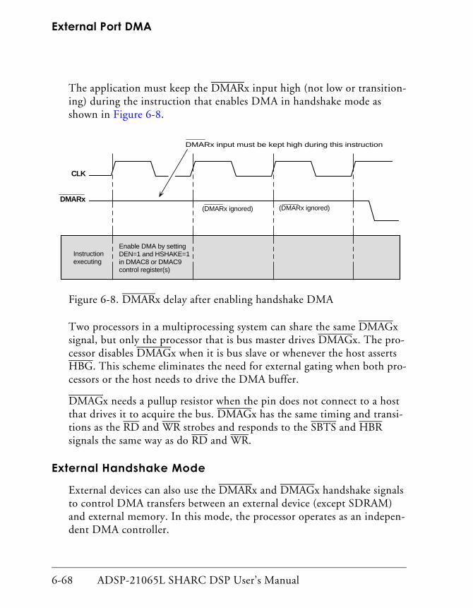
External Port DMA
6-68 ADSP-21065L SHARC DSP User’s Manual
The application must keep the DMARx input high (not low or transition-ing) during the instruction that enables DMA in handshake mode as shown in Figure 6-8.
Figure 6-8. DMARx delay after enabling handshake DMA
Two processors in a multiprocessing system can share the same DMAGx signal, but only the processor that is bus master drives DMAGx. The pro-cessor disables DMAGx when it is bus slave or whenever the host asserts HBG. This scheme eliminates the need for external gating when both pro-cessors or the host needs to drive the DMA buffer.
DMAGx needs a pullup resistor when the pin does not connect to a host that drives it to acquire the bus. DMAGx has the same timing and transi-tions as the RD and WR strobes and responds to the SBTS and HBR signals the same way as do RD and WR.
External Handshake Mode
External devices can also use the DMARx and DMAGx handshake signals to control DMA transfers between an external device (except SDRAM) and external memory. In this mode, the processor operates as an indepen-dent DMA controller.
(DMARx ignored) (DMARx ignored)
DMARx input must be kept high during this instruction
CLK
DMARx
Instructionexecuting
Enable DMA by settingDEN=1 and HSHAKE=1in DMAC8 or DMAC9control register(s)

ADSP-21065L SHARC DSP User’s Manual 6-69
DMA
To configure a channel for external handshake mode, you set the follow-ing bits in the DMACx control register:
EXTERN =1
HSHAKE =1
MASTER =0
These transfers are similar to standard DMA transfers, but with a few differences:
• In external handshake mode, transfers require the DMA controller to generate external memory access cycles.
• DMARx and DMAGx retain the same functionality, but instead of simply generating DMAGx, the processor also outputs addresses, MS3-0 memory selects, and the RD and WR strobes, and it responds to ACK.
The processor holds DMAGx low until the ACK line is released or any wait states finish.
• The access to external memory behaves exactly as if the processor’s core requested it.
The processor’s EPBx buffers do not latch or drive any data, how-ever, and the processor’s DMA controller performs no internal memory DMA transfer.
• To generate the external memory addresses and word count, you must preload the DMA channel’s EIEP, EMEP, and ECEP param-eter registers.
• Since internal DMA transfers do not occur in this mode, you cannot use the PCI bit of the CPEP register to disable the DMA interrupt. Instead, you must use the IMASK register.
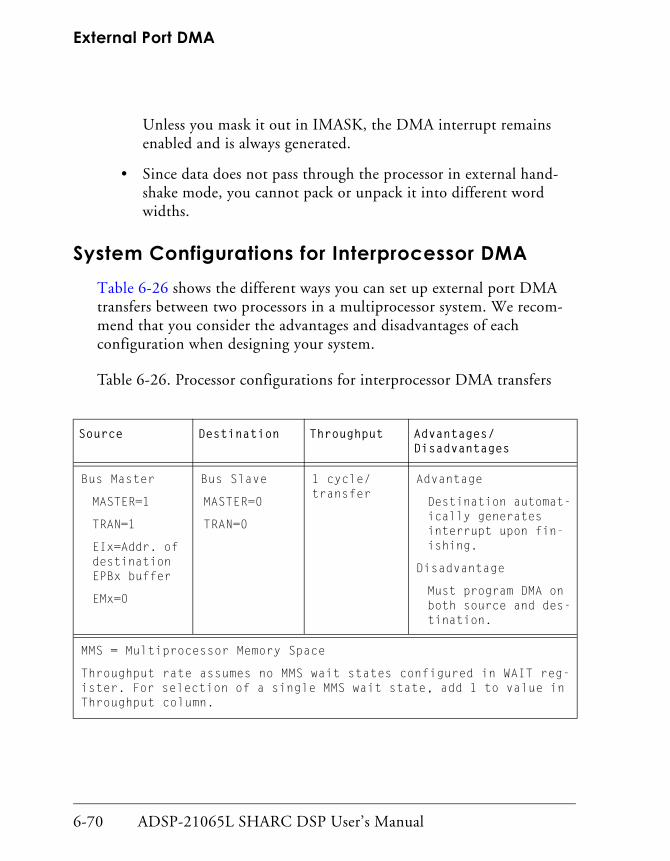
External Port DMA
6-70 ADSP-21065L SHARC DSP User’s Manual
Unless you mask it out in IMASK, the DMA interrupt remains enabled and is always generated.
• Since data does not pass through the processor in external hand-shake mode, you cannot pack or unpack it into different word widths.
System Configurations for Interprocessor DMATable 6-26 shows the different ways you can set up external port DMA transfers between two processors in a multiprocessor system. We recom-mend that you consider the advantages and disadvantages of each configuration when designing your system.
Table 6-26. Processor configurations for interprocessor DMA transfers
Source Destination Throughput Advantages/Disadvantages
Bus Master
MASTER=1
TRAN=1
EIx=Addr. of destination EPBx buffer
EMx=0
Bus Slave
MASTER=0
TRAN=0
1 cycle/ transfer
Advantage
Destination automat-ically generates interrupt upon fin-ishing.
Disadvantage
Must program DMA on both source and des-tination.
MMS = Multiprocessor Memory Space
Throughput rate assumes no MMS wait states configured in WAIT reg-ister. For selection of a single MMS wait state, add 1 to value in Throughput column.

ADSP-21065L SHARC DSP User’s Manual 6-71
DMA
Bus Slave
MASTER=0
TRAN=1
Bus Master
MASTER=1
TRAN=0
EIx=Addr. of source EPBx buffer
EMx=0
2 cycles/ transfer
Advantage
Source automati-cally generates interrupt upon fin-ishing.
Disadvantage
Slower throughput.
Must program on both source and destina-tion.
Table 6-26. Processor configurations for interprocessor DMA transfers (Cont’d)
Source Destination Throughput Advantages/Disadvantages
MMS = Multiprocessor Memory Space
Throughput rate assumes no MMS wait states configured in WAIT reg-ister. For selection of a single MMS wait state, add 1 to value in Throughput column.

External Port DMA
6-72 ADSP-21065L SHARC DSP User’s Manual
Interfacing with DMA HardwareFigure 6-9 shows a typical DMA interface between two multiprocessing ADSP-21065Ls and an external device.
Figure 6-9. Example DMA hardware interface
In this example, both processors are configured for handshake mode operation.
Both external latches act as a mailbox between the external device and the processors. The latches enable DMA transfers to take only one processor
001
010
RD
WR
ACK
MS3-0
HBR
HBG
ID2-0
BR1
BR2ADDR23-0
DATA31-0
DMAR1
DMAG1
DMAR2
DMAG2
ADSP-21065
D Q
OE
Latch
RD
WR
ACK
MS3-0
HBR
HBG
ID2-0
BR1
BR2
ADDR23-0
DATA31-0
DMAR1
DMAG1
DMAR2
DMAG2
ADSP-21065
D Q
OE
Latch
ADDR
DATA
OE
WE
ACK
CS
ExternalMemory
16, 32, or 48
16, 32, or 48 DMA Data Bus
DMA Data Bus
DMA Read Req.
DMA Read Grant
DMA Write Req.
DMA Write Grant
Com
mon
Req
. Lin
e
Com
mon
Gra
nt L
ine
5
3
5
3

ADSP-21065L SHARC DSP User’s Manual 6-73
DMA
bus cycle, even when the external device is slow. The DMARx and DMAGx signals control the latches directly.
When the external device is writing data to a latch, it uses the DMAGx signal as the output enable signal for the latch. When the external device is reading from a latch, it uses the DMAGx signal to clock the data on its ris-ing edge.
Figure 6-10 shows the timing relationships between DMARx, DMAGx, and the data transfer. See the processor’s data sheet for exact specifications.
Figure 6-10. DMARx and DMAGx timing

Overall DMA Throughput
6-74 ADSP-21065L SHARC DSP User’s Manual
Overall DMA ThroughputThis section describes the overall DMA throughput when several DMA channels try to access internal or external memory at the same time.
Concurrent Accesses to Internal MemoryThe DMA channels arbitrate for access to the processor’s internal memory.
The DMA controller determines, on a cycle-by-cycle basis, which channel gains access to the internal I/O bus and, consequently, which channel gets to read or write to internal memory. Table 6-15 on page 6-36 shows the priority of the DMA channels.
Each DMA transfer takes only one clock cycle, even when the DMA con-troller grants different DMA channels access on sequential cycles. That is, switching between channels incurs no loss in overall throughput. So, four serial port DMA channels, each transferring one byte per cycle, would have the same I/O transfer rate as one external port DMA channel trans-ferring data to internal memory on every cycle. Any combination of serial port and external port transfers has the same maximum transfer rate.
Concurrent Accesses to External Memory When the DMA transfer is between the processor’s internal and external memory, the transfer to external memory may incur one or more wait states.
External memory wait states, however, do not reduce the overall internal DMA transfer rate if other channels have data available to transfer. That is, uncompleted external transfers do not hold up the processor’s internal I/O data bus.
ADSP-21065L SHARC DSP User’s Manual 6-75
DMA
For data transfers from internal memory to external memory, the DMA controller places the data in the external port’s EPBx buffer first and then begins the access to external memory independently. (Likewise, for exter-nal-to-internal DMA, the DMA controller does not make the internal DMA request until the data from external memory is in the EPBx buffer.)
In both cases, the external DMA address generator—the EIEP and EMEP parameter registers—maintains the external address until the data transfer has finished. The internal and external address generators of each DMA channel operate independently.
Since EXTERN mode DMA transfers between an external device and external memory do not use the processor’s internal resources, they do not affect internal DMA throughput.

Overall DMA Throughput
6-76 ADSP-21065L SHARC DSP User’s Manual
ASDP-21065L SHARC DSP User’s Manual 7-1
7 MULTIPROCESSINGFigure 7-0.
Table 7-0.
Listing 7-0.
The processor includes functionality and features that enable users to design multiprocessing DSP systems. These features include
• Distributed on-chip bus arbitration logic for bus mastership.
This feature enables the processor to access external memory and the IOP registers of another ADSP-21065L in the system.
• Bus locking capability.
This feature enables the processor to perform indivisibleread-modify-write sequences for semaphores.
In a multiprocessor system with two processors sharing the external bus (see Figure 7-1 on page 7-2), either of the processors can become the bus master. Unless it relinquishes control to the host, the bus master controls the external bus, which consists of the DATA31-0, ADDR23-0, and associ-ated control lines. The bus master always retains control of the SDRAM control pins—CAS, DQM, MSx, RAS, SDA10, SDCKE, SDCLKx, and SDWE.

7-2 ASDP-21065L SHARC DSP User’s Manual
Figure 7-1. A basic multiprocessing system
ADDR23-0
DATA31-0
ADSP-21065L#1
CLKIN
RESET
ID1-0
CPA
BR1
BR2
RD
WR
ACK
MS3-0
BMS
SBTS
SW
CS
HBR
HBG
REDY
RAS
CAS
DQM
SDWE
SDCLK1-0SDKE
SDA10
CONTROL
ADDR23-0
DATA31-0
CLKIN
RESET
ID1-0
CPA
BR1
BR2
ADSP-21065L#2
RAS
CAS
DQM
WE
CLK
CKE
A10
SDRAM(Optional)
ADDRDATACS
ADDR
DATA
BootEPROM
(Optional)
CS
RESET
Clock
01
10
ADDR
DATA
Host Processor(Optional)
CO
NT
RO
L
DA
TA
AD
DR
ES
S
CS
SPORT0
SPORT1
CONTROL
SPORT0
SPORT1
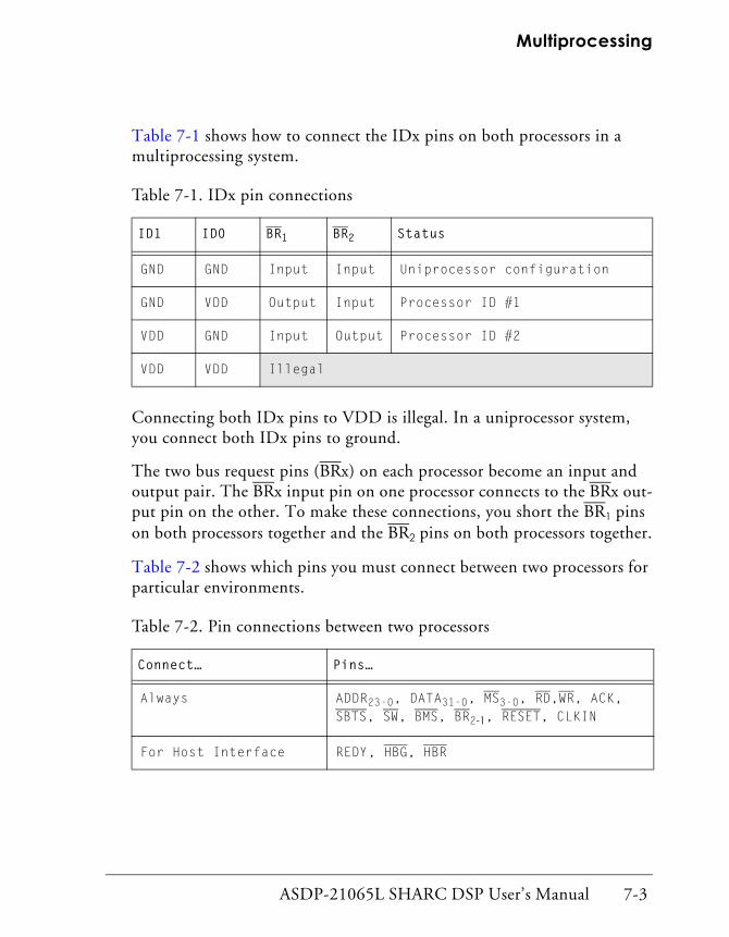
ASDP-21065L SHARC DSP User’s Manual 7-3
Multiprocessing
Table 7-1 shows how to connect the IDx pins on both processors in a multiprocessing system.
Connecting both IDx pins to VDD is illegal. In a uniprocessor system, you connect both IDx pins to ground.
The two bus request pins (BRx) on each processor become an input and output pair. The BRx input pin on one processor connects to the BRx out-put pin on the other. To make these connections, you short the BR1 pins on both processors together and the BR2 pins on both processors together.
Table 7-2 shows which pins you must connect between two processors for particular environments.
Table 7-1. IDx pin connections
ID1 ID0 BR1 BR2 Status
GND GND Input Input Uniprocessor configuration
GND VDD Output Input Processor ID #1
VDD GND Input Output Processor ID #2
VDD VDD Illegal
Table 7-2. Pin connections between two processors
Connect… Pins…
Always ADDR23-0, DATA31-0, MS3-0, RD,WR, ACK, SBTS, SW, BMS, BR2-1, RESET, CLKIN
For Host Interface REDY, HBG, HBR

7-4 ASDP-21065L SHARC DSP User’s Manual
The IOP registers of the system’s processors collectively are called multi-processor memory space. Multiprocessor memory space is mapped into the unified address space of each processor. For details, see Chapter 5‚ Memory.
Once a processor becomes the bus master, it can directly read and write any of the slave’s IOP registers, including its external port FIFO data buff-ers. For example, the master processor can write to a slave’s IOP registers to set up DMA transfers or to send a vector interrupt.
The following terms are used throughout this chapter:
DMACx control registersThe DMA control registers for the EPBx external port buffers DMAC0-1, which correspond to EPB0-1, respectively. For details, see Chapter 6‚ DMA and Appendix E‚ Control and Status Registers in ADSP-21065L SHARC DSP Technical Reference.
External busACK, ADDR23-0, BMS, CAS DATA31-0, DQM, MS3-0, RAS, RD, SDA10, SBTS, SDCKE, SDCLK1-0, SDWE, SW, and WR signals.
External port FIFO buffersEPB1-0, the IOP registers used for external port DMA transfers and single-word data transfers from another processor or from a host. The EPBx buffers are 6-deep FIFOs.
For SDRAM systems CAS, DQM,RAS, SDA10, SDCKE, SDCLK0-1, SDWE
For Core Priority Access Functions
CPA
Table 7-2. Pin connections between two processors (Cont’d)
Connect… Pins…
ASDP-21065L SHARC DSP User’s Manual 7-5
Multiprocessing
IOP registerOne of the control, status, or data buffer registers of the processor’s on-chip I/O processor.
Master processorThe processor that has gained control of the bus from the other ADSP-21065L or from a host.
Multiprocessor memory spaceMemory map area that corresponds to the IOP registers of the other processor in a multiprocessing system. This address space is mapped into the processor’s unified address space.
Multiprocessor systemA system with two processors and with or without a host. The external bus connects both processors.
Single-word data transfersReads and writes to the EPBx external port buffers, performed externally by the master processor or internally by the slave proces-sor’s core. These accesses occur only when DMA has been disabled in the DMACx control register.
Slave processorThe processor that has relinquished control of the bus to the other ADSP-21065L or to a host.
For multiprocessing operations, the processor uses the sys-tem clock which runs at 1xCLKIN. Hereafter, in this chapter, all clock cycle references are to 1xCLKIN, unless otherwise noted.
For details on clock cycles and data throughput, see Table 12-11 on page 12-30.

Multiprocessing System Architecture
7-6 ASDP-21065L SHARC DSP User’s Manual
Multiprocessing System ArchitectureThe nodes in a multiprocessor system communicate through a single, shared global memory over a parallel bus.
Multiprocessing systems must overcome two problems—interprocessor communication overhead and data bandwidth bottlenecks. The proces-sor’s architecture supports two basic multiprocessing topologies that address these problems:
• Data flow multiprocessing
• Cluster multiprocessing
Data Flow MultiprocessingFor applications that require high computational bandwidth, but only limited flexibility, data flow multiprocessing is the best solution.
In this scenario, you partition your algorithm sequentially across both processors and pass data linearly across them, as shown in Figure 7-2.
Figure 7-2. Data flow multiprocessing
The processor is ideally suited for data flow multiprocessing applications because it eliminates the need to use interprocessor data FIFOs and exter-nal memory. For most applications using this topology, the processor’s internal memory is usually sufficient to contain both code and data.
%#+2(!
D
%#+2(!
D
#
+#
+
#
+
#
+
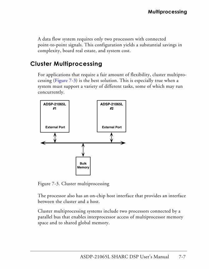
ASDP-21065L SHARC DSP User’s Manual 7-7
Multiprocessing
A data flow system requires only two processors with connected point-to-point signals. This configuration yields a substantial savings in complexity, board real estate, and system cost.
Cluster MultiprocessingFor applications that require a fair amount of flexibility, cluster multipro-cessing (Figure 7-3) is the best solution. This is especially true when a system must support a variety of different tasks, some of which may run concurrently.
Figure 7-3. Cluster multiprocessing
The processor also has an on-chip host interface that provides an interface between the cluster and a host.
Cluster multiprocessing systems include two processors connected by a parallel bus that enables interprocessor access of multiprocessor memory space and to shared global memory.
%#+2(!
D
%#+2(!
D
,0 +,0 +
.E
"7
Multiprocessing System Architecture
7-8 ASDP-21065L SHARC DSP User’s Manual
In a typical cluster, two processors and a host can arbitrate for the bus. The on-chip bus arbitration logic enables these processors to share the par-allel bus. The processor’s on-chip features help reduce the need for extra hardware in the cluster configuration. This configuration often eliminates the need for external memory, both local and global.
The processor supports a fixed priority scheme, bus locking, timed release, and core access preemption of background DMA transfers. The on-chip bus arbitration logic ensures that bus mastership transitions incur only one cycle of overhead. Processor accesses of an external address automati-cally generate a bus request. These extensive bus sharing features free designers from the time and risk involved in developing their own shared-bus logic and timing.
Once a processor gains bus mastership, it can access external memory or the IOP registers of the other processor. To transfer data to the other pro-cessor, the bus master sets up a DMA channel for the transfer.
Both processors are mapped into a common memory map. Each has a unique ID, which identifies its address space within the unified memory map of the system cluster. Both processor’s IOP registers and external memory are part of this unified address space. Memory mapping elimi-nates the need for external memory to pass messages between processors, and it simplifies software communications. Since processors can write directly into each other’s IOP registers, it saves an extra transfer step.
The processor’s on-chip SRAM helps to eliminate the need for local mem-ory. Larger applications, however, may require storing blocks of data and code in shared bulk memory and swapping them in and out of a proces-sor’s internal memory transparently.
The cluster configuration enables a very fast node-to-node data transfer rate. It also enables a simple and efficient software communications model. For example, one processor can perform all of the required setup operations for a DMA transfer, insuring that the other processor com-pletes the DMA transfer uninterrupted.
ASDP-21065L SHARC DSP User’s Manual 7-9
Multiprocessing
The architecture of the processor’s internal memory supports the I/O needs of multiprocessor systems (for details, see Chapter 5‚ Memory). The on-chip, dual-ported RAM enables full-speed interprocessor transfers con-current with dual accesses by the processor’s computational core. These transfers steal no cycles from the core, and the processor continues to exe-cute at 2xCLKIN.

Multiprocessor Bus Arbitration
7-10 ASDP-21065L SHARC DSP User’s Manual
Multiprocessor Bus ArbitrationTwo processors share the external bus with no additional arbitration cir-cuitry. The processor’s on-chip bus arbitration logic enables connection of two processors and a host.
The BR2-1, HBR, and HBG signals provide bus arbitration. BR2-1 arbi-trate between the processors, and HBR and HBG pass control of the bus between the master processor and the host. Table 7-3 lists and describes the pins the processor uses in a multiprocessing system.
Table 7-3. Multiprocessing signals
Signal Type Definition
BR2-1 I/O/S Multiprocessing Bus Requests.
Used by multiprocessing processors to arbi-trate for bus mastership. A processor drives its own BRx line only (corresponding to the value of its ID1-0 inputs) and monitors all others.
ID1-0 I Multiprocessing ID.
Determines which multiprocessing bus request (BR2-1) the processor uses. ID=01 corre-sponds to BR1, ID=10 corresponds to BR2. ID=00 used in single-processor systems.
These lines are a system configuration selection and are hardwired or changed at reset only.

ASDP-21065L SHARC DSP User’s Manual 7-11
Multiprocessing
The ID1-0 pins provide a unique identity for each processor in a multipro-cessing system. Assign one processor ID= 01 and the other ID=10. (For the bus synchronization scheme to function properly, you must assign one processor ID= 01.) Processor 01 holds the external bus control lines stable during reset.
When the ID1-0 inputs of a processor are equal to 01 or 10, the processor configures itself for a multiprocessor system and maps its internal memory and IOP registers into the multiprocessor memory space. ID=00 config-ures the processor for a single-processor system. ID=11 is reserved, so do not use it.
Reading the CRBM (2:0) bits of the SYSTAT register, both processors in a multiprocessor system can determine which processor is the current bus master. These bits contain the value of the ID1-0 inputs of the current bus master.
CPA (o/d) I/O Core Priority Access.
Asserting its CPA pin enables the slave’s core to interrupt background DMA transfers of the other processor and access the exter-nal bus.
CPA is an open drain output that connects to both processors in the system. The CPA pin has an internal 5 KΩ pull-up resistor.
If not required in the system, leave the CPA pin unconnected.
A=Asynchronous;(a/d)=Active Drives; I=Input; O=Output;(o/d)=Open Drain; S = synchronous
Table 7-3. Multiprocessing signals (Cont’d)
Signal Type Definition
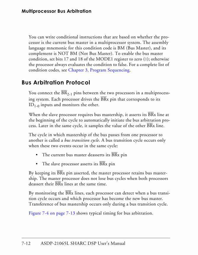
Multiprocessor Bus Arbitration
7-12 ASDP-21065L SHARC DSP User’s Manual
You can write conditional instructions that are based on whether the pro-cessor is the current bus master in a multiprocessor system. The assembly language mnemonic for this condition code is BM (Bus Master), and its complement is NOT BM (Not Bus Master). To enable the bus master condition, set bits 17 and 18 of the MODE1 register to zero (0); otherwise the processor always evaluates the condition to false. For a complete list of condition codes, see Chapter 3‚ Program Sequencing.
Bus Arbitration ProtocolYou connect the BR2-1 pins between the two processors in a multiprocess-ing system. Each processor drives the BRx pin that corresponds to its ID1-0 inputs and monitors the other.
When the slave processor requires bus mastership, it asserts its BRx line at the beginning of the cycle to automatically initiate the bus arbitration pro-cess. Later in the same cycle, it samples the value of the other BRx line.
The cycle in which mastership of the bus passes from one processor to another is called a bus transition cycle. A bus transition cycle occurs only when these two events occur in the same cycle:
• The current bus master deasserts its BRx pin
• The slave processor asserts its BRx pin
By keeping its BRx pin asserted, the master processor retains bus master-ship. The master processor does not lose bus cycles when both processors deassert their BRx lines at the same time.
By monitoring the BRx lines, each processor can detect when a bus transi-tion cycle occurs and which processor has become the new bus master. Transference of bus mastership occurs only during a bus transition cycle.
Figure 7-4 on page 7-13 shows typical timing for bus arbitration.
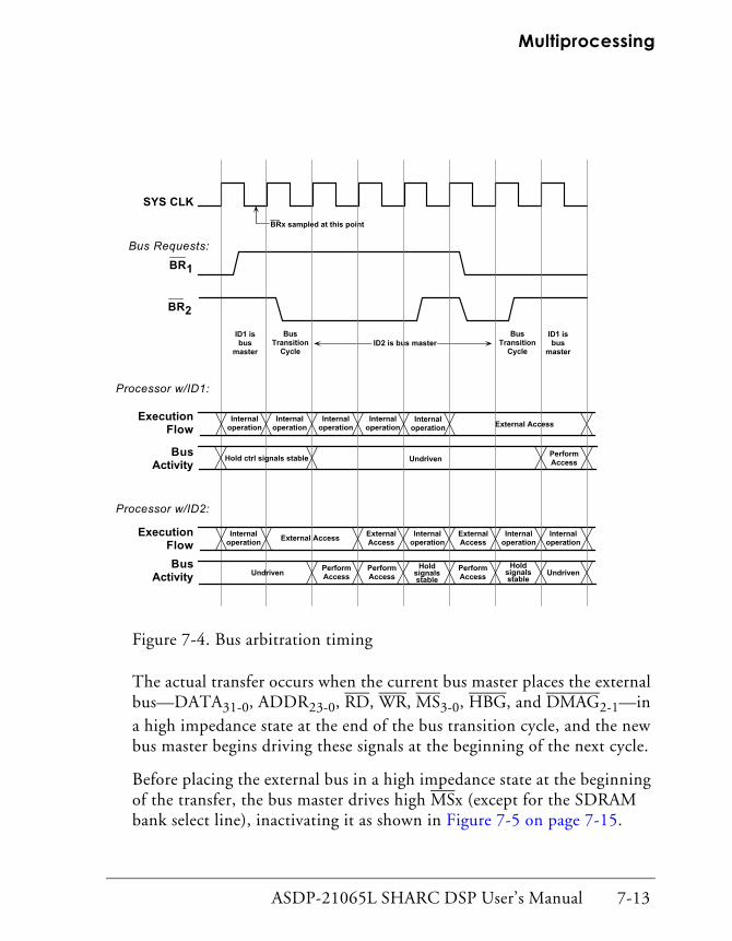
ASDP-21065L SHARC DSP User’s Manual 7-13
Multiprocessing
Figure 7-4. Bus arbitration timing
The actual transfer occurs when the current bus master places the external bus—DATA31-0, ADDR23-0, RD, WR, MS3-0, HBG, and DMAG2-1—in a high impedance state at the end of the bus transition cycle, and the new bus master begins driving these signals at the beginning of the next cycle.
Before placing the external bus in a high impedance state at the beginning of the transfer, the bus master drives high MSx (except for the SDRAM bank select line), inactivating it as shown in Figure 7-5 on page 7-15.
!" #$
%$! &'
(
()!"
!" #$
)!
"
)!
"
" "
!$*#
%$! &'
!$*#
" "
" "
" "
" "
%" $$
+","$$
- "* .$"/ )
" "
%" $$ " "
%" $$
%" $$
" "
" "
- "* +","$$
+","$$
+","$$
- "* .
/ )
./ )
Multiprocessor Bus Arbitration
7-14 ASDP-21065L SHARC DSP User’s Manual
Execution of external accesses are delayed during bus transition cycles. For example, when the slave processor needs to perform an external read or write, and it asserts its BRx line to automatically initiate the bus arbitra-tion process, the read or write is delayed until the processor receives bus mastership.
If the processor’s core, not the DMA controller, generates the read or write, program execution stops until the instruction finishes.
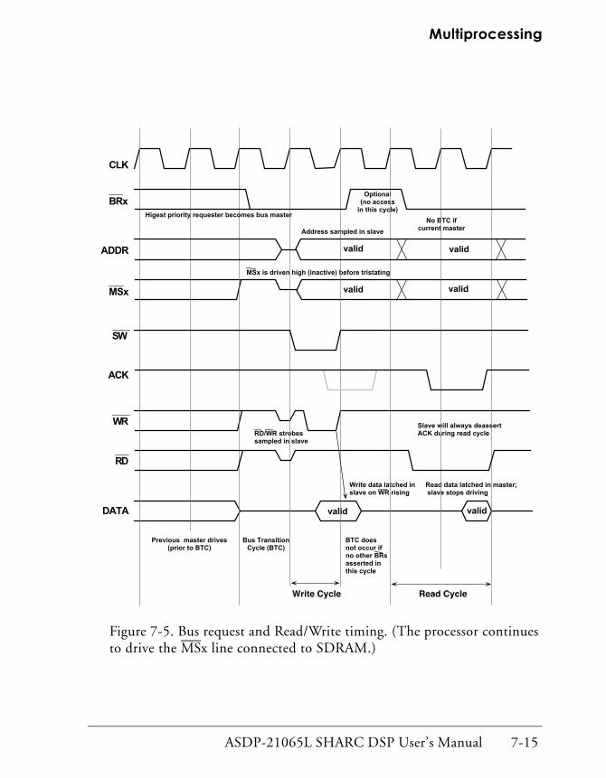
ASDP-21065L SHARC DSP User’s Manual 7-15
Multiprocessing
Figure 7-5. Bus request and Read/Write timing. (The processor continues to drive the MSx line connected to SDRAM.)
" *
0 1 $$ $#$2
,$!"" "
**
*''#"!" /"$#$
!" #$12
3
* *
3"$ * 3" /
$ "4*"* /
+"*!""*1""2
$$!", "" $#$
53") *
3
"* /1 $*2),"" /
./""#"6!")$)!"
* *

Multiprocessor Bus Arbitration
7-16 ASDP-21065L SHARC DSP User’s Manual
To acquire bus mastership and perform an external read or write over the bus, the slave processor:
1. Determines if the instruction that it is executing requires an off-chip access.
2. Asserts its BRx line at the beginning of the cycle.
Until the slave acquires bus mastership, the processor’s core or DMA controller generates extra cycles.
3. Waits for the current bus master to deassert its BRx line and ini-tiate a bus transition cycle.
At the end of the bus transition cycle, the current bus master releases the bus, and the new bus master starts driving it.
Whenever the bus master stops using the bus, it deasserts its BRx line, enabling the other processor to gain mastership if needed. If the slave pro-cessor does not assert its BRx line when the master deasserts its, the master processor retains control of the bus and continues to drive the memory control signals until:
• It needs to use the bus again.
or
• The slave processor asserts its BRx line.
Whenever it executes a conditional external access, the processor attempts to become bus master, even if the access aborts.

ASDP-21065L SHARC DSP User’s Manual 7-17
Multiprocessing
While waiting to acquire bus mastership and perform a DMA transfer, the slave processor asserts its BRx line. If the slave’s core accesses the DMA address (DA) group of IOP registers, the processor deasserts its BRx line until the core completes its access. For a list of the registers in the DA group, see Table E-11 on page E-33, and, for a list of all IOP register groups, see Table E-15 on page E-43, in ADSP-21065L SHARC DSP Technical Reference.
Bus Mastership Timeout You may want to limit how long a bus master can own the bus. To do so, you force the bus master to deassert its BRx line after a specified number of cycles, giving the slave processor a chance to acquire bus mastership.
To set up a bus master timeout, load the BMAX register as follows.
BMAX = (2 * maximum # of CLKIN cycles) – 2
As an example to ensure that any processor retains the bus for a maximum of 10 CLKIN cycles when another slave is requesting the bus, BMAX can be cal-culated as follows.
BMAX = (2 * 10) - 2 = 18
In SDRAM systems, the current master processor asserts its BRx line if the SDRAM controller needs to perform a refresh opera-tion, or the application sets the self-refresh bit in the IOCTL reg-ister. It continues to assert its BRx line until the SDRAM device enters into self-refresh mode.
For SDRAM accesses, the current master processor continues to assert its BRx line if the SDRAM device is still bursting data. In this case, the current master processor deasserts its BRx line such that the SDRAM device stops its data burst before the end of the bus transition cycle.
Multiprocessor Bus Arbitration
7-18 ASDP-21065L SHARC DSP User’s Manual
The minimum value for BMAX is 2, which enables the processor to retain bus mastership for 4 CLKIN cycles.
Each time the processor acquires bus mastership, it loads the value in BMAX into its BCNT register. The processor decrements BCNT each 2xCLKIN cycle in which it performs a read or write over the bus and the slave processor requests the bus. Any time the master processor deasserts its BRx line, it reloads BCNT from BMAX.
When BCNT decrements to zero (0), the bus master:
1. Completes its off-chip read or write.
2. Deasserts its own BRx line, delaying any new off-chip accesses.
This procedure initiates the transfer of bus mastership. If the slave proces-sor is deasserting its BRx request line when the master’s BCNT reaches 0, the master processor keeps asserting its BRx line and does not reload BNCT from BMAX. If the ACK signal is holding off an access when BCNT reaches 0, the master processor retains bus mastership until that access finishes.
If BCNT reaches 0 while bus lock is active, the master processor deasserts its BRx line only after the bus lock is removed. (The BUSLK bit in the MODE2 register enables bus lock. See “Bus Lock and Semaphores” on page 7-34.)
While the master processor is servicing HBR, it stops decrementing BCNT until the host deasserts HBR.
Core Priority AccessAs shown in Figure 7-6 on page 7-19, the Core Priority Access signal, CPA, enables the slave’s core to access the external bus and take priority over ongoing DMA transfers.

ASDP-21065L SHARC DSP User’s Manual 7-19
Multiprocessing
Figure 7-6. Core priority access timing
Normally, during external port DMA transfers, the slave’s core cannot use the external bus until the DMA transfer has finished. By asserting its CPA pin, however, the slave processor’s core can acquire the bus without wait-ing for the DMA operation to finish.
If the CPA signal isn’t used in a multiprocessor system, the master proces-sor relinquishes the bus to the slave processor only when one of the following occurs:
• A cycle in which the master processor does not perform an external bus access
• A bus timeout
If a slave processor needs to send a high priority message or perform an important data transfer, usually, it must wait until any DMA operation finishes. But the CPA signal enables the slave to perform its higher priority bus access with less delay.
"6!
#
+
"$$"6!)# ,"$"
"$$"6! #
12!" #$1! )!"$"$$2
!"","$"$$
')!"/ "+ ,","($#$
+$/ $#$
+"*!!
#"$"'!$"$$ /"

Multiprocessor Bus Arbitration
7-20 ASDP-21065L SHARC DSP User’s Manual
When the slave processor has a pending core access of the bus, it asserts both its CPA pin and its bus request (BRx) pin. CPA is an open-drain out-put and connects both processors in a system. Both processors have a 5 KΩ pull-up resistor on this pin, enabling them to share it. Either proces-sor can assert CPA, and the internal resistors (or an additional external resistor for quicker pull-up) pull it high when it’s released. Both proces-sors can assert this line at the same time.
When CPA is active, the current master processor deasserts its BRx line and relinquishes the bus, providing its core does not have an external access pending. The current bus master never asserts CPA because it already has control of the bus.
In the cycle (≥1 cycle for SDRAM systems, see page 7-19) after the slave asserts CPA, only the processor’s core with a pending external access asserts its bus request. Bus arbitration now proceeds as usual when the pre-vious bus master releases its BRx line.
The processor that becomes bus master releases CPA immediately, the pull-up resistors pull the CPA signal high, and arbitration proceeds nor-mally. The previous bus master, having deasserted its BRx line in response to CPA, reasserts BRx in the cycle after it samples CPA high.
In summary, when a slave processor uses its CPA signal, the following sequence occurs: (see Figure 7-6 on page 7-19)
1. The slave processor asserts both its CPA pin and its BRx pin when its core has an external bus access pending.
2. When the common CPA line is asserted, the master processor, if its core has no external accesses pending, deasserts its BRx line in the next cycle and relinquishes the bus after completing its current access. (≥1 cycle for SDRAM systems, see page 7-19)

ASDP-21065L SHARC DSP User’s Manual 7-21
Multiprocessing
3. In the cycle after the slave asserts CPA, arbitration occurs normally between the processors when both assert their respective BRx lines.
4. The new master processor releases CPA immediately after acquiring the bus.
Both processors arbitrate as usual while CPA is asserted, but each asserts its BRx line only if its core needs to make an access over the external bus.
When CPA is released, both processors resume normal BRx operation one cycle after sampling CPA high. After releasing its CPA, the new bus master ignores the CPA pin for two cycles. This reduces the possibility of losing bus mastership unnecessarily while the common pull-up resistors pull the CPA signal high. Because a resistor, which may have a time constant greater than one cycle, pulls up CPA, both processors may not detect CPA high in the same cycle.
In systems that do not require core access priority, leave the CPA pin unconnected. The processors will arbitrate normally.
Bus Arbitration Synchronization After ResetWhen you use the RESET pin to reset a multiprocessing system, the bus arbitration logic on each processor must resynchronize to insure that only one processor drives the external bus.
During synchronization, one processor becomes the bus master, and the other processor acknowledges it. Synchronization must occur before the processors can actively arbitrate for the bus. The bus synchronization scheme also enables the system to safely bring each processor in and out of reset.
A soft reset (SRST) also resynchronizes the processor.
For the bus synchronization scheme to function properly, you must assign one processor in the system ID=01. The processor with ID1 holds the external bus control lines stable during reset. When the processor is

Multiprocessor Bus Arbitration
7-22 ASDP-21065L SHARC DSP User’s Manual
assigned ID=00 (single-processor mode), it disables bus arbitration synchronization.
After reset, both processors follow this procedure to resynchronize their bus arbitration logic and define the bus master:
1. The processor with ID=10 deasserts its BR2 line during reset and for at least two cycles after, until its bus arbitration logic is synchronized.
After reset, a processor considers itself synchronized in the cycle in which it detects only one BRx line asserted.
The BRx line that is asserted identifies the bus master, and both processors update their internal records (CRBM bits in the SYS-TAT register) accordingly.
2. The processor with ID= 01 asserts its BR1 line during and at least one cycle after reset.
If its BR1 line remains the only one asserted during reset and the following cycle, this processor drives the memory control lines to prevent glitches in their signals. (This processor does not perform reads or writes over the bus.)
If this processor is synchronized by the end of the two cycles fol-lowing reset, it becomes the bus master. If not, it deasserts BR1 and waits until it is.
When a processor has synchronized itself, it sets the BSYN bit in the SYSTAT register.
The processor with ID=01 maintains correct logic levels on the RD, WR, MS3-0, HBG, and the SDRAM signals—CAS, DQM, RAS, SDA10, SCCLK, SDCKE, and SDWE—during reset.

ASDP-21065L SHARC DSP User’s Manual 7-23
Multiprocessing
Because an erroneous write to the soft reset bit (SRST) in the SYSCON register can reset the processor with ID=01, that processor behaves this way during reset:
1. It asserts BR1 to gain control of the bus.
2. It drives the RD, WR, MS3-0, DMAG1, DMAG2, HBG, and the SDRAM signals—CAS, DQM, RAS, SDA10, SCCLK, SDCKE, and SDWE—only if it determines it has control of the bus.
Two conditions determine whether the processor has control of the bus:
• In the previous cycle, BR1 was asserted and BR2 was deasserted,
and
• In the previous cycle, HBG was deasserted.
The processor with ID=01 continues to drive the RD, WR, MS3-0, DMAG1, DMAG2, and HBG and the SDRAM signals—CAS, DQM, RAS, SDA10, SCCLK, SDCKE, and SDWE—for two cycles after reset, as long as neither HBG nor BR2 are asserted. At the end of the second cycle, the processor assumes bus mastership if it is synchronized, and normal bus arbitration begins in the following cycle. If it remains unsynchronized, the processor deasserts BR1, stops driving the memory control signals, and does not arbitrate for the bus until it becomes synchronized.
Although the bus synchronization scheme supports reset of individual processors, the processor with ID=01 may fail to drive the memory control signals if it is in reset while the processor with ID=10 asserts its BR2 line.
If the processor with ID= 01 has asserted HBG while it is in reset, it becomes synchronized when the host or external RESET circuitry deas-serts RESET. This protocol enables the host to use the bus while the processors are in reset.

Multiprocessor Bus Arbitration
7-24 ASDP-21065L SHARC DSP User’s Manual
If a host attempts to reset the master processor (which is driving the HBG output), the host immediately loses control of the bus.
During reset, the master processor pulls the ACK line high with an inter-nal 2 kΩ equivalent resistor.

ASDP-21065L SHARC DSP User’s Manual 7-25
Multiprocessing
Data TransfersThe master processor can read and write all of the slave processor’s IOP registers to:
• Control and configure the slave’s operation (SYSCON and SYS-TAT registers).
• Communicate with the slave’s core (MSGRx).
• Send a vector interrupt (VIRPT).
• Set up DMA transfers (DMACx).
• Transfer data.
To do so, the master processor reads or writes the address of the appropri-ate IOP register in multiprocessor memory space.
The slave processor monitors the address lines driven on the external bus and responds to any address that falls within its region of multiprocessor memory space.
These accesses are invisible to the slave’s core because they are performed through the external port, over the on-chip I/O bus—not the DM bus or PM bus. This is an important distinction, because it enables the slave’s core to continue executing program uninterrupted. (See Figure 8-1 on page 8-2.)
For heavily loaded buses, or when using external data buffers, you can add a single wait state to all multiprocessor memory accesses. To do so, you set the MMSWS bit in the WAIT register. (For details, see “Multiprocessor Memory Space Wait States and Acknowledge” on page 5-61.)

Data Transfers
7-26 ASDP-21065L SHARC DSP User’s Manual
Writing the IOP Registers
When the master processor writes to a slave processor, the slave’s I/O pro-cessor latches the address and data on-chip, buffering the address and data in a special set of FIFO buffers, the slave write FIFO, at the external port pins (see Figure 8-1 on page 8-2). If the master processor attempts addi-tional writes when this FIFO buffer is full, the slave processor deasserts ACK until the buffer is no longer full.
In the next cycle after the slave’s I/O processor latches the address and data, the slave write FIFO attempts to complete the write internally to the target IOP register. This enables the master processor to perform writes at the full clock rate.
Writes to the IOP registers usually occur in the following one or two cycles. Writes take more than two cycles only when a full buffer delayed a write in the previous cycle.
If the EPBx buffer and the slave write FIFO are full when the master pro-cessor attempts a write, the slave deasserts ACK until buffer space is available. The EPBx buffer usually empties within one cycle, creating a write latency, unless higher priority, on-chip DMA transfers are in progress.
Data in the slave write FIFO delays a master processor read. This delay prevents the master processor from reading invalid data and from per-forming operations out of sequence.
Because the external port buffers (EPBx), which are also IOP reg-isters, are six-deep FIFO buffers, writes to them execute slightly differently than writes to the other IOP registers. And, the mas-ter processor uses them to perform DMA transfers. For details, see “Transfers Through the EPBx Buffers” on page 7-27.
ASDP-21065L SHARC DSP User’s Manual 7-27
Multiprocessing
Reading the IOP RegistersWhen the master processor reads a slave processor, the slave’s I/O proces-sor latches the address on-chip, and the slave asserts ACK. When the slave processor reads the corresponding IOP register location, it drives the data off-chip and asserts ACK. Unlike writes, the processor cannot pipeline reads. Reads occur one at a time only.
Writes have a maximum pipelined throughput of one per cycle, and reads have a maximum throughput of one every one 1xCLKIN cycle. See Chapter 12‚ System Design. Because of this low bandwidth, direct reads are not the most efficient method of transferring data out of a slave processor.
Transfers Through the EPBx BuffersIn addition to reads and writes of the other IOP registers, the master pro-cessor can transfer data to and from the slave processor’s internal memory space through its external port FIFO buffers, EPB0 and EPB1.
Through the EPBx buffers, the master processor can perform:
• Single-word transfers
The processor’s core handles internal single-word transfers.
• DMA block transfers
The processor’s DMA controller handles internal DMA transfers.
Each EPBx buffer has a read port and a write port. Both ports can connect internally to the EPD (External Port Data) bus, the IOD (I/O Data) bus, the PM Data bus, or the DM Data bus as shown in Figure 7-1 on page 7-2.
When the master processor writes to the slave processor’s EPBx buffers, the slave’s I/O processor latches and buffers the address and data on-chip,
Data Transfers
7-28 ASDP-21065L SHARC DSP User’s Manual
just as it does for writes to the other IOP registers. And, if additional writes occur when the slave write FIFO buffer is full, the slave deasserts ACK and waits for space to become available in the buffer.
But, because both of the EPBx buffers, which are part of the IOP register set, are six-location FIFOs, the master processor can perform up to six writes before encountering a delay, or write latency. (The external port FIFO buffers can be delayed up to four cycles if all of the serial port DMA channels are active or up to nine cycles per chain during a DMA chaining operation.)
Single-Word Transfers
When the master processor writes a single data word to a slave’s EPBx buffers, the slave’s core must read the data. Conversely, when the slave’s core writes a single piece of data to one of its EPBx buffers, the master processor must perform an external bus read cycle to obtain it. Because the EPBx buffers are six-deep, bidirectional FIFOs, the cores of both proces-sors have extra time to read the data. This functionality enables efficient, continuous, single-word transfers to occur in real-time, with low latency and no DMA.
If the master processor attempts to read from an empty EPBx buffer on the slave, the slave holds off the access with the ACK signal until the buffer receives data from the core. If the slave’s core attempts to write to a full EPBx buffer, the slave processor delays the access, and its core hangs until the master processor reads the buffer. To prevent the slave’s core from hanging, set the Buffer Hang Disable bit (BHD=1) in the SYSCON register. To determine the status of a particular EPBx buffer, read the appropriate DMACx register.
Similarly, if the master processor attempts to write to a full EPBx buffer on the slave processor, the slave delays the access with ACK until its core reads the buffer. If the slave’s core attempts to read from an empty buffer, the slave processor delays the access, and its core hangs until the master
ASDP-21065L SHARC DSP User’s Manual 7-29
Multiprocessing
processor writes the buffer. To prevent this hang condition, set BHD=1 in the SYSCON register.
To flush (clear) either EPBx buffer, write 1 to the FLSH bit in the corre-sponding DMACx control register. The processor does not latch this bit internally, and this bit always reads as 0.
Status can change in the following cycle.
Do not enable and flush an EPBx buffer in the same cycle.
Interrupts for Single-Word Transfers. You can use the interrupts for the two external port DMA channels to control single-word data transfers between the master processor and the slave.
To do so, set two bits in the DMACx control register:
DEN=0 Disables DMA
INTIO=1 Enables interrupt-driven I/O DMA interrupts
For details, see Chapter 6‚ DMA and Appendix E‚ Control and Status Registers in ADSP-21065L SHARC DSP Technical Reference.
With this configuration, the interrupt is generated whenever data becomes available in the read port of the EPBx buffer or whenever the write port has no new data to transmit. Then, either the slave’s core or an external device, such as the master processor or host, can read or write the EPBx buffer. Generating interrupts this way is useful for implementing inter-rupt-driven I/O that the slave’s core controls.
You can mask out (disable) this interrupt in the IMASK register. If you re-enable it later in IMASK, make sure you clear the corresponding
To perform single-word, non-DMA transfers through the EPBx buffers, you must clear the DMA enable bit (DEN) in the appro-priate DMACx control register.

Data Transfers
7-30 ASDP-21065L SHARC DSP User’s Manual
IRPTL latch bit to clear any interrupt request that might have occurred in the interim, before you re-enabled the interrupt.
DMA Transfers
The master processor can also set up DMA transfers to and from a slave’s internal memory space. The master processor writes to the slave’s DMA control and parameter registers to set up an external port DMA operation. This is the most efficient way to transfer blocks of data between two processors.
• DMA transfers to internal memory space .
The master processor sets up external port DMA channels to trans-fer data to and from the slave’s internal memory space, or it can use the DMA request and grant lines (DMARx and DMAGx) to transfer data directly to or from the slave’s internal memory space.
• DMA transfers to external memory space.
Using the DMA request and grant lines (DMARx and DMAGx), the master processor sets up an external port DMA channel to transfer data directly to the slave’s external memory space.
See Chapter 6‚ DMA for details on setting up DMA operations.
Transfers to Internal Memory Space. To set up DMA channels to transfer data to and from the slave’s internal memory space, the master processor initializes the slave’s DMA control and parameter registers for the particu-lar channel. Once the DMA channel is set up, the master processor reads from or writes to the corresponding EPBx buffer on the slave.
If the slave’s EPBx buffer is empty (or full), the access is extended until data is available (or stored). This method enables fast and efficient data transfers.
ASDP-21065L SHARC DSP User’s Manual 7-31
Multiprocessing
The master processor sets up a channel for either slave mode DMA or for handshake mode DMA. To do so, the it sets the MASTER, HSHAKE, and EXTRERN bits in the channel’s DMACx register appropriately.
For slave mode DMA, it sets:
MASTER = 0
HSHAKE = 0
EXTERN = 0
In slave mode DMA, if the buffer is empty (or full), the slave’s DMA con-troller extends the access until data is available (or stored). This method enables fast and efficient data transfers.
To pack and unpack DMA data, you select the packing mode in the PMODE bits of the external port DMA control registers (DMAC0 and DMAC1).You can select 16-bit to 32- or 48-bit and 32-to-48-bit packing and unpacking. For details, see “External Port DMA Data Packing” on page 6-51.
For handshake mode DMA, it sets:
MASTER = 0
HSHAKE = 1
EXTERN = 0
In handshake mode DMA, the master processor can also use the DMARx and DMAGx handshake signals for a DMA transfer.
DMA Transfers to External Memory Space. To use the slave’s DMA con-troller to transfer data directly to external memory space, you must use the external handshake mode for external port DMA channel 8 or 9.
Data Transfers
7-32 ASDP-21065L SHARC DSP User’s Manual
For external handshake mode DMA, set:
MASTER =0
HSHAKE = 1
EXTERN = 1
This mode provides the DMARx and DMAGx handshaking for this type of transfer.
Since the data passes through the DMA controller and not the processor, you cannot pack the data.
For details on using DMA, see Chapter 6‚ DMA.
Interacting with the Shadow Write FIFOBecause the processor’s internal memory must operate at high speeds, writes to the memory do not go directly into the memory array, but into a two-deep FIFO called the Shadow Write FIFO.
When an internal memory write cycle occurs, the processor loads into memory the data in the Shadow Write FIFO and loads the new data into the Shadow Write FIFO. Normally, this operation is transparent since the processor intercepts and routes to the FIFO any reads of the last two loca-tions written. You need be aware of the Shadow Write FIFO only when you mix 48- and 32-bit word accesses to the same locations in memory.
The Shadow Write FIFO cannot differentiate between the mapping of 48-bit words and the mapping of 32-bit words. (See Figure 5-10 on page 5-32.) So, if you write a 48-bit word to memory and try to read the data with a 32-bit word access, the Shadow Write FIFO will not intercept the read, and the processor will return incorrect data.
ASDP-21065L SHARC DSP User’s Manual 7-33
Multiprocessing
If you must mix 48- and 32-bit accesses to the same locations, flush out the Shadow Write FIFO with two dummy writes before you attempt to read the data.
Bus Lock and Semaphores
7-34 ASDP-21065L SHARC DSP User’s Manual
Bus Lock and SemaphoresYou can use semaphores in multiprocessor systems to enable both proces-sors to share resources, such as memory or I/O.
A semaphore is a flag that either processor sharing the resource can read and write. The value of the semaphore indicates when the processor can access the resource. Semaphores are also useful for synchronizing the tasks each processor is performing separately.
The bus lock feature enables the processor to read and modify a sema-phore in a single indivisible operation—a key requirement of multiprocessing systems.
Semaphores can reside in external memory or in an IOP register, such as a message register (MSGRx). When attempting a read-modify-write opera-tion on a semaphore, a processor must have bus mastership for the duration of the operation. If both processors obey this rule, both can per-form read-modify-write operations on semaphores.
A processor adheres to this rule when it uses its bus lock feature to lock in its mastership of the bus. Doing so, it prevents the other processor from simultaneously accessing the semaphore.
To request bus lock, you set the BUSLK bit in the MODE2 register. Then, the processor initiates the bus arbitration process, asserting its BRx line. When it becomes bus master, the processor locks the bus, keeping its BRx line asserted, even when not performing an external read or write, to maintain its bus mastership. The processor ignores HBR during a bus lock. When the BUSLK bit is cleared, the processor deasserts its BRx line to relinquish control of the bus.
While the BUSLK bit is set, the processor can execute a conditional instruction using the BM or NOT BM condition codes to determine who is current bus master. For example:
IF NOT BM JUMP(PC,0);/* wait for bus mastership */

ASDP-21065L SHARC DSP User’s Manual 7-35
Multiprocessing
If it is not the current bus master, the processor can either wait until it gains control of the bus, or it can clear its BUSLK bit and try again later. If it is the current bus master and the semaphore resides in external mem-ory space, the processor can proceed with reading or writing the semaphore. If it is the current bus master and the semaphore resides in IOP register space, the processor must test the status of the SWPD bit (SYSTAT register) before proceeding to read or write the semaphore.
In summary, to perform a read-modify-write operation, write code that follows these steps:
1. Set the BUSLK bit in MODE2 to request a bus lock.
2. Wait to acquire bus mastership.
If the semaphore resides in IOP register space, wait until SWPD=0.
3. Read the semaphore, test it, then write to it.

Interprocessor Messages
7-36 ASDP-21065L SHARC DSP User’s Manual
Interprocessor MessagesTo communicate with the slave processor, the master processor writes messages to the slave’s IOP registers.
The MSGR7-0 registers are general-purpose registers, which applications can use to pass messages or to implement semaphores and resource sharing between two processors.
You can use the MSGRx and VIRPT registers for interprocessor commu-nications in the following ways:
• Message Passing
The master processor can read or write any of the slave’s eight mes-sage registers, MSGR7-0, to pass messages.
• Vector Interrupts
The master processor can write the address of an interrupt service routine to the slave’s VIRPT register to generate a vector interrupt.
Doing so causes an immediate, high-priority interrupt on the slave that, when serviced, causes the slave processor to branch to the spec-ified service routine.
The MSGRx and VIRPT registers also support the host interface. Since these registers can be shared resources within a single processor, conflicts can occur. Your system software is responsible for preventing such con-flicts. For details, see Appendix E‚ Control and Status Registers, in ADSP-21065L SHARC DSP Technical Reference.

ASDP-21065L SHARC DSP User’s Manual 7-37
Multiprocessing
Message Passing (MSGRx)The master processor has three software protocols available to it for com-municating with a slave through the slave’s MSGRx message registers:
• Vector-interrupt-driven
The master fills predetermined MSGRx registers on the slave with data and writes the address of the service routine to the slave’s VIRPT register to trigger a vector interrupt.
After the slave’s service routine reads the data from the MSGRx reg-isters, it must write 0 to VIRPT to tell the master it has completed the read.
• Register handshake
You designate four of the MSGRx registers as follows:
• A receive register (R)
• A receive handshake register (RH)
• A transmit register (T)
• A transmit handshake register (TH).
Register handshaking follows this sequence:
1. To pass data to the slave processor, the master processor writes data into T and then writes 1 into TH.
2. When the slave processor sees 1 in TH, it reads the data from T and then writes 0 back into TH.
The service routine can also use one of the slave’s FLAG11-0 pins to tell the master it has finished.

Interprocessor Messages
7-38 ASDP-21065L SHARC DSP User’s Manual
3. When the master processor sees 0 in TH, it knows that the trans-fer has finished.
4. The slave processor follows a similar sequence when it passes data to the master processor through R and RH.
• Register write-back
This method is similar to the register handshake method, but uses only the T and R data registers.
Register write-back follows this sequence:
1. The master processor writes data to T.
2. When the slave processor sees a nonzero value in T, it retrieves it and writes 0 back into T.
3. The master processor uses a similar sequence to receive data.
This method is simpler and works well as long as the data to pass does not include 0.
Vector Interrupts (VIRPT)The processor uses vector interrupts to respond to interprocessor com-mands from the other processor or from a host. When the other processor or an external device writes an address to the processor’s VIRPT register, it generates a vector interrupt.
Servicing a Vector Interrupt
When it services a vector interrupt, the processor automatically pushes the status stack and begins executing the service routine located at the address specified in VIRPT. The lower twenty-four bits of VIRPT contain the address. Optionally, you can use the upper eight bits to pass data for the

ASDP-21065L SHARC DSP User’s Manual 7-39
Multiprocessing
interrupt service routine to read. At reset, the processor reinitializes VIRPT to its standard address in the interrupt vector table.
The minimum latency for vector interrupts is six cycles, five of which are NOPs. When the interrupt service routine reaches the RTI (return from interrupt) instruction, the processor automatically pops the status stack.
Make sure your interrupt service routine checks the VIPD bit in the SYS-TAT register. This bit indicates the status of the VIRPT register:
• If the master processor writes the slave’s VIRPT while a previous vector interrupt is pending, the new vector address replaces the pending one.
• If the master processor writes the slave’s VIRPT while the slave is servicing a previous occurrence of the vector interrupt, the slave ignores the new vector address, so the write doesn’t generate a new interrupt.
• If the processor writes to its own VIRPT register, the write doesn’t generate an interrupt.
To use the slave processor’s vector interrupt feature, the master processor performs this procedure:
1. Polls the slave’s VIRPT register until it reads a certain token value (for example, 0).
2. Writes the vector interrupt service routine address to VIRPT.
When the service routine is finished, the slave processor writes the token back into VIRPT to indicate that it has finished and that it is ready to accept another vector interrupt.
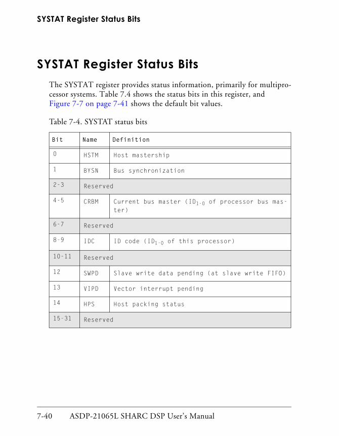
SYSTAT Register Status Bits
7-40 ASDP-21065L SHARC DSP User’s Manual
SYSTAT Register Status BitsThe SYSTAT register provides status information, primarily for multipro-cessor systems. Table 7.4 shows the status bits in this register, and Figure 7-7 on page 7-41 shows the default bit values.
Table 7-4. SYSTAT status bits
Bit Name Definition
0 HSTM Host mastership
1 BYSN Bus synchronization
2-3 Reserved
4-5 CRBM Current bus master (ID1-0 of processor bus mas-ter)
6-7 Reserved
8-9 IDC ID code (ID1-0 of this processor)
10-11 Reserved
12 SWPD Slave write data pending (at slave write FIFO)
13 VIPD Vector interrupt pending
14 HPS Host packing status
15-31 Reserved
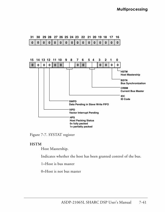
ASDP-21065L SHARC DSP User’s Manual 7-41
Multiprocessing
Figure 7-7. SYSTAT register
HSTMHost Mastership.
Indicates whether the host has been granted control of the bus.
1=Host is bus master
0=Host is not bus master
/()/
()/()
9 @-
.#7@A
$
$.
F -+
9+ E#
87- E
8- 7- E
+# C; ;
SYSTAT Register Status Bits
7-42 ASDP-21065L SHARC DSP User’s Manual
BSYN Bus Synchronization.
Indicates when the processor’s bus arbitration logic is synchronized after reset. (See “Bus Arbitration Synchronization After Reset” on page 7-21.)
1=Synchronized
0=Not synchronized
CRBMCurrent Bus Master.
Indicates the ID code of the processor that is the current bus mas-ter. If CRBM is equal to the ID of this processor then it is the current bus master. CRBM is only valid for ID2-0 > 0 (greater than zero). When ID2-0=00, CRBM is always 1.
IDC ID Code.
Indicates the ID2-0 inputs of this processor.
SWPDSlave write pending data.
Indicates valid data is pending in the slave write FIFO.
1=Data pending
0=No data pending
VIPD Vector Interrupt Pending.
Indicates that a pending vector interrupt has not yet been serviced.
The VIPD bit is set when the VIRPT register is written to and is cleared upon return from the interrupt service routine.

ASDP-21065L SHARC DSP User’s Manual 7-43
Multiprocessing
The master processor (or host) that issued the vector interrupt should monitor this bit to determine when the service routine has finished, and when a new vector interrupt can be issued.
1=Vector interrupt pending
0=No vector interrupt pending
HPS Host Packing Status.
Indicates when host word packing is completed or, if not, what stage of the process is taking place.
0=Partially packed
1=Fully packed

SYSTAT Register Status Bits
7-44 ASDP-21065L SHARC DSP User’s Manual

ADSP-21065L SHARC DSP User’s Manual 8-1
8 HOST INTERFACEFigure 8-0.
Table 8-0.
Listing 8-0.
The host interface provides an asynchronous connection to standard 8-, 16-, and 32-bit microprocessor buses and supports asynchronous transfers at speeds up to 1xCLKIN.
The host interface enables a host to:
• Gain control of the processor and its external bus.
Once in control the host can access any of the processor’s resources.
• Read and write any of the processor’s IOP registers, including the EPBx FIFO buffers.
All of the internal IOP registers and resources of any processor’s I/O processor are available to the host. The host uses specific IOP con-trol and status registers to control and configure the processor and to set up DMA transfers. Once set up, the processor’s on-chip DMA controller controls DMA transfers.
• Transfer code and data to and from the processor over the two exter-nal port DMA channels.
DMA transfers incur low software overhead.
• Pack and unpack 8-, 16-, and 32- bit host data to and from 32- or 48-bit internal data.
• Use interprocessor messages and vector interrupts to ensure host commands execute efficiently.
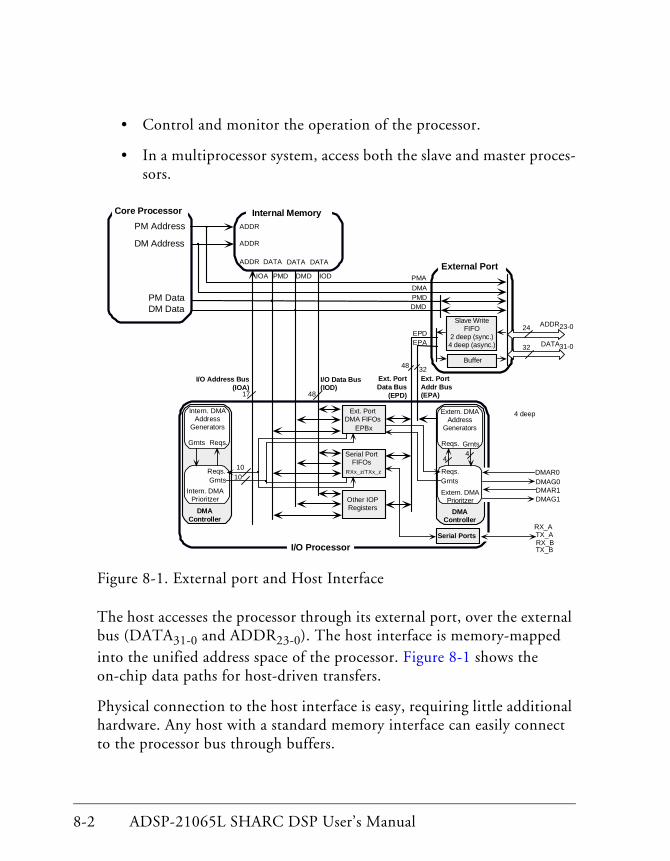
8-2 ADSP-21065L SHARC DSP User’s Manual
• Control and monitor the operation of the processor.
• In a multiprocessor system, access both the slave and master proces-sors.
Figure 8-1. External port and Host Interface
The host accesses the processor through its external port, over the external bus (DATA31-0 and ADDR23-0). The host interface is memory-mapped into the unified address space of the processor. Figure 8-1 shows the on-chip data paths for host-driven transfers.
Physical connection to the host interface is easy, requiring little additional hardware. Any host with a standard memory interface can easily connect to the processor bus through buffers.
I/O Processor
Intern. DMAAddress
Generators
Grnts Reqs.
Intern. DMAPrioritzer
Reqs.Grnts
DMAController
Ext. PortDMA FIFOs
EPBx
Serial PortFIFOs
RXx_z/TXx_z
Other IOPRegisters
Extern. DMAAddress
Generators
GrntsReqs.
Extern. DMAPrioritzer
Reqs.Grnts
DMAController
Serial Ports
44
ADDR
DATA DATA
ADDR
Internal Memory
ADDR DATA
17
I/O Address Bus(IOA)
Core Processor
External Port
Slave WriteFIFO
2 deep (sync.)4 deep (async.)
Buffer
ADDR23-024
32 DATA31-0
PM Address
DM Address
PM DataDM Data
4 deep
48
I/O Data Bus(IOD)
48 32
PMADMA
DMDPMD
IOA IODPMD DMD
Ext. PortData Bus
(EPD)
EPAEPD
Ext. PortAddr Bus(EPA)
DMAR1DMAG1
DMAR0DMAG0
TX_ARX_A
RX_BTX_B
1010

ADSP-21065L SHARC DSP User’s Manual 8-3
Host Interface
Table 8-1 lists and describes the pins used to interface with a host.
Table 8-1. Host interface pins
Pin Type Definition
HBR I/A Host Bus Request.
Host must assert this pin to request control of the processor’s external bus.
In a multiprocessing system, when the host asserts HBR, the processor that is bus mas-ter relinquishes the bus and asserts HBG.
To relinquish the bus, the processor places the address, data select, and strobe lines in a high-impedance state.
HBR has priority over all processor bus requests, BRx, in a multiprocessing system.
HBG I/O Host Bus Grant.
The processor asserts HBG to acknowledge an HBR bus request and indicate that the host can take control of the external bus. The processor holds HBG low until the host releases HBR.
In a multiprocessing system, only the master processor outputs HBG.
CS I/A Chip Select.
Host asserts to select a processor.
A = Asynchronous; (a/d) = Active Drive; I=Input; O = Output; (o/d) = Open Drain; S = Synchronous
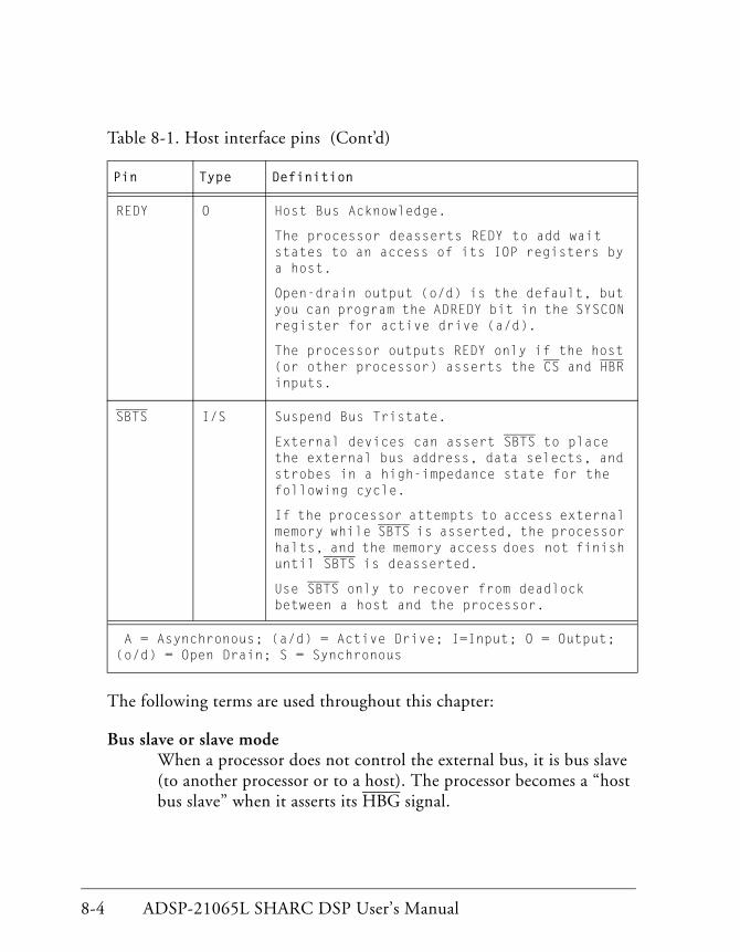
8-4 ADSP-21065L SHARC DSP User’s Manual
The following terms are used throughout this chapter:
Bus slave or slave modeWhen a processor does not control the external bus, it is bus slave (to another processor or to a host). The processor becomes a “host bus slave” when it asserts its HBG signal.
REDY O Host Bus Acknowledge.
The processor deasserts REDY to add wait states to an access of its IOP registers by a host.
Open-drain output (o/d) is the default, but you can program the ADREDY bit in the SYSCON register for active drive (a/d).
The processor outputs REDY only if the host (or other processor) asserts the CS and HBR inputs.
SBTS I/S Suspend Bus Tristate.
External devices can assert SBTS to place the external bus address, data selects, and strobes in a high-impedance state for the following cycle.
If the processor attempts to access external memory while SBTS is asserted, the processor halts, and the memory access does not finish until SBTS is deasserted.
Use SBTS only to recover from deadlock between a host and the processor.
Table 8-1. Host interface pins (Cont’d)
Pin Type Definition
A = Asynchronous; (a/d) = Active Drive; I=Input; O = Output; (o/d) = Open Drain; S = Synchronous
ADSP-21065L SHARC DSP User’s Manual 8-5
Host Interface
Bus transition cycle (BTC)In a multiprocessor system, a cycle in which control of the external bus passes from one processor to another.
Cluster busIn a multiprocessor system, the path connecting one processor’s external bus to the other’s. See also, External bus.
DMACx control registersDMA control registers for the EPBx external port buffers: DMAC0 and DMAC1 correspond to EPB0 and EPB1, respectively (see Chapter 6, DMA, and Appendix E, Control and Status Registers, in ADSP-21065L SHARC DSP Technical Reference).
DMA transfersInternal transfers of data blocks that the processor’s DMA control-ler, not its core, handles.
External busThe processor’s ACK, ADDR23-0, BMS, CAS, DATA31-0, DQM, MS3-0, RAS, RD, SDA10, SBTS, SDCKE, SDCLK0-1, SDWE, SW, and WR, signals.
External port FIFO buffersEPBx buffers. A host or another processor uses these IOP registers for external port DMA transfers and single-word data transfers. These buffers are six-deep FIFOs.
Host A host microprocessor.
Host transfersAsynchronous accesses of the processor by the host. After acquiring control of the processor’s external bus, the host must assert the CS pin of the processor it wants to access.

8-6 ADSP-21065L SHARC DSP User’s Manual
Host transition cycle (HTC)A cycle in which control of the external bus passes from the proces-sor to the host. During this cycle, the processor stops driving the RD, WR, ADDR23-0, MS3-0 (except the MSx line connected to an SDRAM device), SW, and DMAGx signals, which the host must then drive.
IOP registerOne of the control, status, or data buffer registers of the processor’s on-chip I/O processor.
Local busIn a multiprocessor system, the path connecting one processor’s external bus to local memory or to a system bus buffer. See also, External bus, Cluster bus.
Master processorThe ADSP-21065L that is bus master.
Multiprocessor systemA system with two processors, with or without a host. The proces-sors connect directly over the external bus.
Multiprocessor memory spacePortion of the processor’s memory map that includes the IOP reg-isters of the other processor in a multiprocessing system. This address space is mapped into the processor’s unified address space.
ProcessorAn ADSP-21065L.
Single-word data transfersReads and writes of the EPBx external port buffers, performed externally by a host or internally by the core. DMA must be dis-abled in the processor’s DMACx control register.

ADSP-21065L SHARC DSP User’s Manual 8-7
Host Interface
Slave processorAn ADSP-21065L that is not bus master.
For operations that involve the host interface, the processor uses the system clock, which runs at 1xCLKIN. Hereafter, in this chapter, all clock cycle references are to 1xCLKIN, unless other-wise noted.
For details on clock cycles and data throughput, see Table 12-19 on page 12-62.
Host Control of the Processor
8-8 ADSP-21065L SHARC DSP User’s Manual
Host Control of the ProcessorThe HBR, HBG, and REDY signals enable a host to gain control of a pro-cessor and its external bus. Once granted control, the host can transfer 8-, 16-, or 32-bit data asynchronously to and from the processor.
Acquiring the BusTo gain access to the processor,
1. The host asserts HBR, the host bus request signal.
HBR has priority over all BRx multiprocessor bus requests. When asserted, HBR causes the current master processor to relinquish the bus to the host as soon as the current bus cycle finishes.
2. The current master processor asserts HBG as soon as the current bus operation finishes to signal that it is transferring control of the bus.
The cycle in which control of the bus transfers is called a host tran-sition cycle (HTC).
Figure 8-2 on page 8-10 shows the timing for bus acquisition by the host.
3. The current master processor continues to assert HBG during the bus transition cycle (BTC), until the host deasserts HBR.
HBG freezes processor/multiprocessor bus arbitration while the host owns the bus. While HBG is asserted, the other processor con-tinues to assert and deassert its BRx line as in normal operation, but no BTCs occur.
The current master processor holds its BRx line low the entire time the host controls the bus.

ADSP-21065L SHARC DSP User’s Manual 8-9
Host Interface
The host should use HBG to enable its signal buffers (see Figure 8-8 on page 8-45.)
Once it has gained control of the bus, the host can initiate asynchronous transfers. To do so, the host:
1. Asserts the CS pin of the processor that it wants to access and per-forms the asynchronous read or write.
2. Drives the ADDR7-0 and either the M address field bits as 0 or any E address field bits as 1 (for details, see Table 5-3 on page 5-20), RD, WR, and SW signals during the HTC in which it gains control of the bus (see Figure 8-3 on page 8-13).
The host must continue to drive these signals for the entire time it owns the bus. In addition, it must either drive the MS3-0 lines (except the MSx line connected to an SDRAM device) and the DMAG1 and DMAG2 grant lines, or these lines must be pulled weakly up or down. (You need pull the DMAGx lines up or down weakly only if they connect externally.) The master processor places these lines in a high impedance state to enable the host to use them.

Host Control of the Processor
8-10 ADSP-21065L SHARC DSP User’s Manual
Figure 8-2. Example timing for bus acquisition
During read-modify-write operations, to avoid temporary loss of bus mas-tership, the host must continue asserting HBR until it completes the last data transfer.
The following restrictions apply to host acquisitions of the bus:
• If the host asserts HBR while the processor is in reset, the processor responds with HBG only after multiprocessor synchronization has finished. If the processor is ID0 (single-processor system), it responds with HBG immediately.
!!
"#$%
&#'!!
&#$
!
!!
!!
%!&#'(
)( $*$
&#'!!
&
+
)&+)
%
%
&
+
)&+)

ADSP-21065L SHARC DSP User’s Manual 8-11
Host Interface
For details, see “Bus Arbitration Synchronization After Reset” on page 7-21.
• The host must not deassert HBR during a host access.
• If SBTS is asserted after HBR, the processor may enter slave mode and suspend any unfinished access to the external bus.
(For details, see “Resolving Bus Access Deadlock” on page 8-49.)
Once the it has finished its task, the host can deassert HBR to relinquish control of the bus. The master processor deasserts HBG in response.
In the next cycle, the master processor regains control of the bus, and nor-mal multiprocessor arbitration resumes. The host must not deassert HBR until after it has completed its last data transfer with the processor.
Host TransfersAfter acquiring control of the processor’s external bus, the host must assert the CS pin of the processor it wants to access. Doing so informs the pro-cessor that it will be transferring data asynchronously with the host. The host must then drive the offset address of the IOP register it wants to access. To simplify hardware requirements for the external interface logic, the host need drive ADDR7-0 only and either the M address field bits as 0 or the appropriate E address field bits as 1 (for M and E address field defi-nitions, see Table 5-3 on page 5-20).
Asynchronous Transfer TimingWhen a host asserts a processor’s CS chip select, the selected processor deasserts the REDY signal with a delay of approximately 10 ns. For exact timing specifications, see the processor’s data sheet.
Host Control of the Processor
8-12 ADSP-21065L SHARC DSP User’s Manual
At this time, CS, not RD or WR, causes the processor to deassert REDY because the host interface buffers for RD and WR may not be enabled if the bus master has not asserted HBG.
The host can assert CS before or after it asserts HBR, but the processor will not reassert REDY until after the bus master has asserted HBG and the host has applied a RD or WR strobe. This is true only if a RD or WR strobe is active when the processor asserts HBG; otherwise, the tTRDYHG switching characteristic determines the timing. (See the timing section of the processor’s data sheet.)
The processor asserts REDY before a RD or WR and deasserts REDY only if it is not ready to complete the read or write. The only exception occurs when the host first asserts CS. The REDY pin defaults to open-drain out-put to facilitate interfacing to common buses. To change it to an active-drive output, set ADREDY=1 in the SYSCON register.
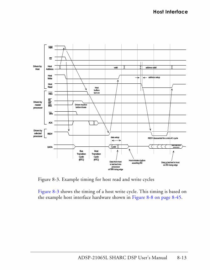
ADSP-21065L SHARC DSP User’s Manual 8-13
Host Interface
Figure 8-3. Example timing for host read and write cycles
Figure 8-3 shows the timing of a host write cycle. This timing is based on the example host interface hardware shown in Figure 8-8 on page 8-45.
HBR
HostAddress
CS
Hostbuffersturn on
valid address valid
HBG
Driven byHost
Driven by master
processor
DATA
BRx
ACK
REDYdata setup
valid
BusTransition
Cycle(BTC)
HostTransition
Cycle(HTC)
REDY deasserted for a min of 1 cycle
valid data fromprocessor
Data from hostis latched into
processoron WR rising edge
Host tristates beforeasserting RD
Driven byselected
processor
Data is latched in hoston RD rising edge
HostWrite
HostRead
RDWRMSx Driven inactive
before trisate
address setup
Host Control of the Processor
8-14 ADSP-21065L SHARC DSP User’s Manual
A host write cycle follows this sequence:
1. The host asserts the address.
Since the system bus interface address comparator decodes HBR and CS, the host need not supply them directly. The selected pro-cessor deasserts REDY immediately.
2. The host asserts WR and drives data (according to the timing requirements specified in the data sheet).
3. The selected processor asserts REDY when it is ready to accept the data.
This occurs after the current bus master has completed its current transfer and has asserted HBG. HBG enables the host interface buffers to drive onto the processor’s bus.
4. The host deasserts WR when REDY is high and stops driving data.
5. The selected processor latches data on the rising edge of WR.
After the first word, the write sequence is:
6. The host asserts WR and drives data (according to the timing requirements specified in the processor’s data sheet).
7. The processor deasserts REDY if it is not ready to accept data.
8. The host deasserts WR when REDY is high and stops driving data.
9. The selected processor latches data on the rising edge of WR.
In a multiprocessor system, if the ADREDY bit is cleared (0) on both pro-cessors, the host can assert both processor’s CS pins at the same time during a write, but not during a read because of bus conflict.

ADSP-21065L SHARC DSP User’s Manual 8-15
Host Interface
To enable full speed asynchronous writes, the processor latches data at the I/O pins in a four-level FIFO buffer, the slave write FIFO (see Figure 8-1 on page 8-2). This buffering enables the processor to resynchronize previ-ously written words while a host is writing a new word, and it enables asynchronous writes to occur at speeds up to 1xCLKIN.
Figure 8-3 on page 8-13 also shows the timing of a host read cycle. This timing is based on the example host interface hardware shown in Figure 8-8 on page 8-45.
A host read cycle follows this sequence:
1. The host asserts the address.
The system bus interface address comparator decodes HBR and the appropriate CS line again. The selected processor deasserts REDY immediately and asserts HBG.
2. The host asserts RD.
3. The selected processor drives data onto the bus and asserts REDY when the data is available.
4. The host latches the data and deasserts RD.
After the first word, the read sequence is:
5. The host asserts RD.
6. The selected processor deasserts REDY then asserts REDY, driving data when it becomes available.
7. The host deasserts RD when REDY is high and latches the data.
The maximum throughput for reads is one every two CLKIN cycles.
Data Transfers
8-16 ADSP-21065L SHARC DSP User’s Manual
Data TransfersThe host or the bus master can read and write all of the I/O processor’s IOP registers to:
• Control and configure the processor’s operation (SYSCON and SYSTAT).
• Communicate with the processor’s core (MSGRx).
• Set up DMA transfers (DMACx).
• Transfer data.
To do so, the host asserts the processor’s CS line and writes the offset address of the IOP register it wants to access in the lower eight bits of the external address bus and writes either 0 to the M address field bits or 1 to the appropriate E address field bits (see Table 5-3 on page 5-20).
These accesses are invisible to the processor’s core because they use the external port and the on-chip I/O bus—not the DM bus or the PM bus (see Figure 8-1 on page 8-2). This is an important distinction because it enables the processor’s core to continue executing program uninterrupted.
Writing to the IOP Registers
When the host writes to a slave processor, the slave’s I/O processor latches the address and data on-chip, buffering the address and data in a special set of FIFO buffers, the slave write FIFO, at the external port pins (see
Because the external port buffers (EPBx), which are also IOP reg-isters, are six-deep FIFO buffers, writes to them execute slightly differently than writes to the other IOP registers. And, the host uses them to perform DMA transfers. For details, see “Transfers Through the EPBx Buffers” on page 8-18.

ADSP-21065L SHARC DSP User’s Manual 8-17
Host Interface
Figure 8-1 on page 8-2). If the host attempts additional writes when this FIFO buffer is full, the processor deasserts REDY until the buffer is no longer full.
In the next cycle after the I/O processor latches the write data, the slave write FIFO attempts to complete the write internally to the target IOP register. This enables the host or master processor to perform writes at the full clock rate.
Writes to the IOP registers usually occur in the following one or two cycles. Writes take more than two cycles only if a full EPBx buffer delayed a write in the previous cycle.
If the EPBx buffer and slave write FIFO are full when the host attempts a write, the processor deasserts REDY until buffer space is available. The EPBx buffer usually empties out within one cycle, creating a write latency, unless higher priority, on-chip DMA transfers are in progress.
Data in the slave write FIFO delays a host read. This delay prevents the host from reading invalid data and from performing operations out of sequence.
Reading the IOP RegistersWhen the host or master processor reads a slave processor, the slave’s I/O processor latches the address on-chip and deasserts REDY. When the slave processor reads the corresponding IOP register location, it drives the data off-chip and asserts REDY. Unlike writes, reads cannot be pipelined; they occur one at a time only.
Writes have a maximum pipelined throughput of one per CLKIN cycle, and reads have a maximum throughput of one every two CLKIN cycles. For details, see Chapter 12, System Design. Because of this low band-width, reads are not the most efficient method of transferring data out of a slave processor.
Data Transfers
8-18 ADSP-21065L SHARC DSP User’s Manual
Transfers Through the EPBx BuffersIn addition to reads and writes of the other IOP registers, the host can transfer data to and from the processor’s internal memory space through its external port FIFO buffers, EPB0 and EPB1.
Through the EPBx buffers, the host can perform:
• Single-word transfers
The processor’s core handles internal single-word transfers.
• DMA block transfers
The processor’s DMA controller handles internal DMA transfers.
Each EPBx buffer has a read port and a write port. Both ports can connect internally to either the EPD (External Port Data) bus, the IOD (I/O Data) bus, the PM Data bus, or the DM Data bus as shown in Figure 8-1 on page 8-2.
When the host writes to a slave processor’s EPBx buffers, the slave’s pro-cessor latches and buffers the address and data on-chip, just as it does for writes to the other IOP registers. And, if additional writes occur when the slave write FIFO buffer is full, the processor deasserts REDY and waits for room in the buffer.
But because both of the EPBx buffers, which are part of the IOP register set, are six-location FIFOs, the host can perform up to six writes before encountering a delay, a write latency. (The external port FIFO buffers can be delayed for up to four CLKIN cycles if all of the serial port DMA chan-nels are active or for up to four CLKIN cycles per chain during a DMA chaining operation.)
ADSP-21065L SHARC DSP User’s Manual 8-19
Host Interface
Single-Word Transfers
When the host writes a single data word to the EPBx buffers, the proces-sor’s core must read the data. Conversely, when the processor’s core writes a single piece of data to one of the EPBx buffers, the host must perform an external read cycle to obtain it. Because the EPBx buffers are six-deep, bidirectional FIFOs, the host and the processor’s core have extra time to read the data. This functionality enables efficient, continuous, single-word transfers to occur in real-time, with low latency and no DMA.
If the host attempts a read from an empty EPBx buffer, the processor holds off the access with the REDY signal until the buffer receives data from the core. If the processor’s core attempts to write to a full EPBx buffer, the processor delays the access, and the core hangs until the host reads the buffer. To prevent the core from hanging, set the Buffer Hang Disable bit (BHD=1) in the SYSCON register. To determine the status of a particular EPBx buffer, read the appropriate DMACx register.
Similarly, if the host attempts a write to a full EPBx buffer, the processor holds off the access with REDY until the processor’s core reads the buffer. If the core attempts to read from an empty buffer, the processor delays the access, and the core hangs until the host writes to the buffer. To prevent this hang condition, set BHD=1 in the SYSCON register. With BHD=1, how-ever, reads may access invalid data, and writes may not finish.
To flush (clear) either EPBx buffer, write a 1 to the FLSH bit in the corre-sponding DMACx control register. The processor does not latch this bit internally, and it always read as 0. Status can change in the following cycle. Do not enable and flush an EPBx buffer in the same cycle.
To pack and unpack individual data words, you must set both the PMODE bits in the appropriate DMACx control register and the HBW bits in the SYSCON register. For details, see Table 8-2 on page 8-24.

Data Transfers
8-20 ADSP-21065L SHARC DSP User’s Manual
For single-word transfers, you must also set the TRAN bit in the EPBx DMACx control register appropriately:
TRAN=1 For host reads of the EPBx register
TRAN=0 For host writes to the EPBx register
Interrupts for Single-Word Transfers. You can use the interrupts for the two external port DMA channels to control single-word data transfers between the host and the processor’s core. To do so, set the DEN and INTIO bits in the DMACx control register:
DEN=0 Disable DMA
INTIO=1 Enable interrupt-driven I/O
For details, see Chapter 6, DMA, and Appendix E, Control and Status Registers, in ADSP-21065L SHARC DSP Technical Reference.
With this configuration, the interrupt is generated whenever data becomes available in the read port of the EPBx buffer or whenever the write port does not have new data to transmit. Then, either the processor’s core or an external device, such as the host, can read or write the EPBx buffer. Gen-erating interrupts this way is useful for implementing interrupt-driven I/O that the processor’s core controls.
You can mask out (disable) this interrupt in the IMASK register. Before you re-enable it in IMASK, make sure you clear the corresponding IRPTL latch bit to clear any interrupt request that might have occurred in the interim.
To perform single-word, non-DMA transfers through the EPBx buffers, you must clear the DMA enable bit (DEN=0) in the appropriate DMACx control register.

ADSP-21065L SHARC DSP User’s Manual 8-21
Host Interface
DMA Transfers
The host can also set up DMA transfers to and from the processor’s inter-nal or external memory space. Once the host has gained control of the processor, it can access the on-chip DMA control and parameter registers to set up an external port DMA operation. This is the most efficient way to transfer blocks of data.
• DMA transfers to internal memory space.
The host can set up external port DMA channels to transfer data to and from the processor’s internal memory space, or it can use the DMA request and grant lines (DMARx, DMAGx) to transfer data directly to or from the processor’s internal memory space.
• DMA transfers to external memory space.
Using the DMA request and grant lines (DMARx, DMAGx), the host can set up an external port DMA channel to transfer data directly to or from the processor’s external memory space.
Transfers to Internal Memory Space. To set up DMA channels to transfer data to and from internal memory space, the host must initialize the pro-cessor’s control and parameter registers for the particular channel. Once the DMA channel is set up, the host simply reads from or writes to the corresponding EPBx buffer.
The hosts sets up a channel for either slave mode DMA or handshake mode DMA. To do so, the host sets the MASTER, HSHAKE, and EXTERN bits in the channel’s DMACx register appropriately.
For slave mode DMA, set:
MASTER = 0
HSHAKE = 0
EXTERN = 0
Data Transfers
8-22 ADSP-21065L SHARC DSP User’s Manual
In slave mode DMA, if the buffer is empty (or full), the processor’s DMA controller extends the access until data is available (or stored). This method enables fast and efficient data transfers.
To pack and unpack DMA data, you select the packing mode in the PMODE bits of the external port DMA control registers (DMAC0 and DMAC1) and the HBW bits in the SYSCON register. See Table 8-2 on page 8-24 for the available packing modes.
For handshake mode DMA, set:
MASTER = 0
HSHAKE = 1
EXTERN = 0
In handshake mode DMA, the host can also use the DMARx and DMAGx handshake signals for a DMA transfer, but not when it has asserted HBR to gain control of the bus.
DMA Transfers to External Memory Space. To use the processor’s DMA controller to transfer data directly from the host to external memory space, you must use the external handshake mode for external port DMA channel 8 or 9.
For external handshake mode DMA, set:
MASTER =0
HSHAKE = 1
EXTERN = 1
This mode provides the DMARx and DMAGx handshaking for this type of transfer.

ADSP-21065L SHARC DSP User’s Manual 8-23
Host Interface
These transfers have the following restrictions:
• The host cannot use HBR to gain control of the bus.
• Since the data passes through the DMA controller and not the pro-cessor, you cannot pack the data.
For details on using DMA, see Chapter 6, DMA.
Performing Broadcast WritesBroadcast writes enable simultaneous transmission of data to both proces-sors in a multiprocessing system. The host can perform broadcast writes to the same IOP register on both processors. You can use broadcast writes to implement semaphores in a multiprocessing system and to simultaneously download code or data to both processors. For details, see “Bus Lock and Semaphores” on page 7-34.
To implement broadcast writes, the host must assert CS on both processors.
During a broadcast write, both processors:
• Accept the write as if either is the only device addressed.
• Use REDY to add wait states to the host’s broadcast write if neces-sary.
The host must wire-OR both processors’ REDY lines together and configure ADREDY in SYSCON for open-drain output.
In this configuration, REDY appears asserted only when both pro-cessors are ready. (This is true only if REDY is not actively pulled up.)

Data Packing
8-24 ADSP-21065L SHARC DSP User’s Manual
Data PackingFor accesses to all IOP registers, except the EPBx buffers, the processor packs and unpacks host data to and from 32-bit internal words. To specify the host’s bus width, you set the HBW bits in the SYSCON register (see Table 8-3 on page 8-26).
For accesses to the EPBx buffers, the host interface has data packing logic to pack 8-, 16-, or 32-bit external host bus words into 32- or 48-bit inter-nal words. The packing logic is reversible to unpack 32-bit or 48-bit internal data into 8-, 16-, or 32-bit external data. Bits in both the DMACx control registers and the SYSCON register determine the data packing mode for EPBx transfers.
To pack and unpack individual data words, you set both the PMODE bits in the appropriate DMACx control register and the HBW bits in the SYSCON register. The PMODE bits determine the width of internal words, and the HBW bits determine the width of external words. Table 8-2 shows the packing modes available with various combinations of the PMODE and HBW bits.
Table 8-2. Packing mode bits for EPBx transfers
DMA Packing Mode Host Bus Width
PMODE Internal bits 00 (32b) 01 (16b) 10 (8b)
00 Invalid for host DMA transfers using the EPBx buffers. Use only with nonhost DMA transfers.
01 32 No pack 16 ↔ 32 8 ↔ 32
10 48 32 ↔ 48 16 ↔ 48 8 ↔ 48
11 Identical to PMODE = 10

ADSP-21065L SHARC DSP User’s Manual 8-25
Host Interface
Packing Control Bits in SYSCONFigure 8-4 shows the SYSCON register bits that affect host data packing and memory width and Table 8-3 on page 8-26 describes them.
Figure 8-4. SYSCON register bits
31 30 29 28 27 26 25 24 23 22 21 20 19 18 17 16
0 0 00000 00000000 0
15 14 13 12 11 10 9 8 7 6 5 4 3 2 1 0
0 0 00000 00001000 0
EBPRExt. Bus Priority00=even01=core processor10=I/O processor
DCPRDMA Chn. 8–9 Priority1=rotating0=sequential
BHDBuffer Hang Disable
0=enable1=disable
ADREDYActive Drive REDY0=open drain (o/p)
1=active drive (a/d)
IMDW1Int. Mem. Blk1
Data Width0=32-bit data1=40-bit data
IMDW0Int. Mem. Blk0
Data Width0=32-bit data1=40-bit data
SRSTSoftware Reset
BSOBoot Select Override
HBWHost Bus Width00=32 bits01=16 bits10=8 bits11=reserved
IIVTInt. Interrupt VectorTable(no boot mode)
HMSWFHost Packing Order-MSW First0=LSW1=MSW
HPFLSHHost PackingStatus Flush
Data Packing
8-26 ADSP-21065L SHARC DSP User’s Manual
After reset, the SYSCON register initializes to 0x0000 0020, which causes the processor to assume an 8-bit bus for the host. To change this selection, you must write four 8-bit words to SYSCON (in the HBW bits), even if the host bus is 16- or 32-bits wide.
Table 8-3. SYSCON control bits
Bit Name Description
4-5 HBW Host packing mode.
Specifies the external word width of the host bus for host accesses to the processor’s IOP registers.
00= 32-bit host bus
01= 16-bit host bus
10= 8-bit host bus
All IOP registers share one 16-bit write latch. The write latch transfers data to the appropriate channel only after it accumu-lates 16-bits. So, to prevent data corrup-tion, the host must write to the processor’s IOP registers in 8-bit word pairs, maintain-ing control of the bus through both writes of a word pair.
11= reserved; invalid value
If the host access is a read or write of any IOP register other than the external port FIFO buff-ers (EPB0 or EPB1), the internal word width is always 32 bits, regardless of the width of the host bus.

ADSP-21065L SHARC DSP User’s Manual 8-27
Host Interface
6 HMSWF Host packing order.
Specifies the packing order of host-accessed words. The I/O processor ignores HMSWF for 32-to-48 bit packing.
0= LSW first
1= MSW first
7 HPFLSH Host packing status flush.
Resets the host packing status. Host accesses must not occur while the processor’s core is writing the HPFLSH bit.
A two cycle latency always occurs before the flush takes effect and the host can resume nor-mal operations.
HPFLSH always reads as 0.
8 IMDW01 Internal memory block 0 data width.
Selects the data word width for block 0 of internal memory.
0= 32-bit data
1= 40-bit data
9 IMDW11 Internal memory block 1 data width.
Selects the data word width for block 1 of internal memory.
0= 32-bit data
1= 40-bit data
1 This bit has no affect on fetches of 48-bit instructions in a memory block. For details, see Chapter 5, Memory.)
Table 8-3. SYSCON control bits (Cont’d)
Bit Name Description
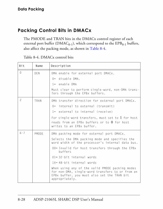
Data Packing
8-28 ADSP-21065L SHARC DSP User’s Manual
Packing Control Bits in DMACxThe PMODE and TRAN bits in the DMACx control register of each external port buffer (DMAC0-1), which correspond to the EPB0-1 buffers, also affect the packing mode, as shown in Table 8-4.
Table 8-4. DMACx control bits
Bit Name Description
0 DEN DMA enable for external port DMACx.
0= disable DMA.
1= enable DMA
Must clear to perform single-word, non-DMA trans-fers through the EPBx buffers.
2 TRAN DMA transfer direction for external port DMACx.
0= internal to external (transmit)
1= external to internal (receive)
For single-word transfers, must set to 1 for host reads from an EPBx buffers or to 0 for host writes to an EPBx buffer.
6-7 PMODE DMA packing mode for external port DMACx.
Selects the DMA packing mode and specifies the word width of the processor’s internal data bus.
00= Invalid for host transfers through the EPBx buffers
01= 32-bit internal words
1X= 48-bit internal words
When using any of the valid PMODE packing modes for non-DMA, single-word transfers to or from an EPBx buffer, you must also set the TRAN bit appropriately.

ADSP-21065L SHARC DSP User’s Manual 8-29
Host Interface
See Table 8-2 on page 8-24 for details on how the PMODE bits and HBW bits combine to affect the packing mode when using the EPBx buffers.
To change the host packing mode, follow these steps:
1. Write to the SYSCON register and change the value of HBW.
2. Read SYSCON to ensure that the write was successful.
Since this read functions as an interlock only, ignore the read data.
3. Repeat step 1 to flush the read since it might have occurred in the previous packing mode.
4. Wait four cycles.
During packed transfers with a slow host, the host can relinquish the bus before the I/O processor has finished packing the current word. That is, the host can release the bus after writing the first part of the word and reassert HBR later to write the second part of the word. You could imple-ment this scheme to enable another processor to write to this processor without the write affecting the host packing operation.

Data Packing
8-30 ADSP-21065L SHARC DSP User’s Manual
Data Bus Lines and Host Bus WidthTable 8-5 shows which data bus lines the processor uses for different host bus widths and packing modes.
If the host bus width is 32 bits and no packing (HBW = 00) is selected for an access, the processor inputs whatever data is on the external bus and drives DATA31-0 with whatever data is in the corresponding memory bits.
If the host bus width is 16 bits and 32 or 48-bit packing (HBW=1x) is selected, the processor ignores the upper 16 bits of the 32-bit external data bus when inputting data, and it drives these bits as 0s when outputting data.
If the host bus width is 8 bits and 32 or 48-bit packing (HBW=1x) is selected, the processor ignores the upper 24 bits of the 32-bit external data bus when inputting data, and it drives these bits as 0s when outputting data.
Table 8-5. Host bus width and data bus lines
HBW Data In Data Out
32 bits Processor inputs and outputs 32-bit data over the external bus (DATA31-0) as is.
16 bits Processor ignores upper 16 bits of the external bus (DATA31-16).
Processor outputs 0s in the upper 16 bits of the exter-nal bus (DATA31-16).
8 bits Processor ignores upper 24 bits of the external bus (DATA31-8).
Processor outputs 0s on the upper 24 bits of the exter-nal bus (DATA31-8).

ADSP-21065L SHARC DSP User’s Manual 8-31
Host Interface
Figure 8-5 shows how the processor transfers different data word sizes over the external port.
Figure 8-5. External port data alignment
32-Bit Data Packing and Unpacking
Using typical bus interface hardware as shown in Figure 8-8 on page 8-45, when a host reads a 32-bit word with 16-bit unpacking, the host performs the following sequence. (See Figure 8-6 on page 8-32 for an example tim-ing diagram of this host read sequence.)
1. The host drives an address, asserting CS, and asserts RD to initiate a read cycle.
2. The selected processor deasserts REDY, latches the address, and performs an internal read to get the data.
3. When the processor has the data, it asserts REDY and drives the first 16-bit word.
4. The host latches the data and deasserts RD.
32-bit Float or FixedD31-D0
32-bit Packed
16-bit Packed
8-bit Packed
EPROMBoot
31 24 16 8 0
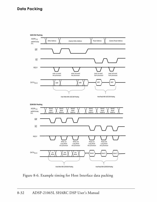
Data Packing
8-32 ADSP-21065L SHARC DSP User’s Manual
Figure 8-6. Example timing for Host Interface data packing
Word1Write
Address
1stWord
Word1
REDY
32/48 Bit Packing
ADDR7-0
DATA31-0
Word1Write
Address
Word2Write
Address
Word1Read
Address
Word2Read
Address
Word2Read
Address
Write 1stLong Word
into processor
Write 2ndLong Word
into processor
Read 1stLong Word
into processor
Read 2ndLong Word
into processor
2ndWord
3rdWord
Word 2 Word 3
Host Write With 32/48 Bit Packing Host ReadWith32/48 Bit Packing
WR
RD
Write Address (Same) Write Address Read Address (Same) Read Address
REDY
write 1st wordinto processor
write 2nd wordinto processor
read 1st wordfrom processor
read 2nd wordfrom processor
valid valid valid valid
16/32 Bit Packing
DATA15-0
Host Write With 16/32 Bit Packing HostRead With16/32Bit Packing
WR
RD
andM=0oranyE=1
ADDR7-0andM=0oranyE=1

ADSP-21065L SHARC DSP User’s Manual 8-33
Host Interface
5. The host initiates another read access, driving the address of the data to access and then asserting RD.
6. The processor transmits the second 16-bit word.
Using typical bus interface hardware as shown in Figure 8-8 on page 8-45, when a the host writes a 32-bit word with 16-bit packing, the host per-forms the following sequence. (See Figure 8-6 on page 8-32 for an example timing diagram of this host write sequence.)
1. The host drives the write address, asserting CS, and asserts WR to initiate a write cycle.
2. The processor asserts REDY when it is ready to accept data.
3. The host drives the address and the first 16-bit word and deasserts WR (high).
4. The processor latches the first 16-bit word.
5. The host drives the same address and asserts WR again to initiate another write cycle for the second 16-bit word.
6. After the processor accepts the second word, it performs an internal write to its IOP register.
If it has not completed the internal write by the time the host tries another access and the slave write FIFO has no space, the processor delays that access with REDY.
While the processor is waiting for another word from the host to complete the packed word, the HPS bits in the SYSTAT register are nonzero. (See “SYSTAT Register Bits” on page 8-40.) Because the Host Interface has only one packing buffer, the host must com-plete each packed read or write before beginning another.
Data Packing
8-34 ADSP-21065L SHARC DSP User’s Manual
For 8-bit hosts, reads and writes follow these same sequences, except that 8-bit hosts must perform four reads or four writes to transfer a 32-bit word.
48-Bit Instruction Packing
Using the EPBx buffers, a host can also download and upload 48-bit instructions over its 8-, 16- or 32-bit bus.
A 32-bit host transfers 32-bit data on DATA31-0. To transfer an odd num-ber of instruction words, you must flush the packing buffer with a dummy access to remove the unused word.
The packing sequence for downloading instructions from a 32-bit host bus takes three cycles for every two words as shown in Table 8-6.
For 32-to-48-bit packing, the processor ignores the HMSWF bit in the SYSCON register.
The packing sequence for downloading or uploading instructions over a 16-bit host bus takes three cycles for every word (see Table 8-7). The
Table 8-6. Host to processor, 32- to 48-bit word packing
Transfer Data bus lines 31-16 Data Bus Lines 15-0
First Word 1; bits 47-32 Word 1; bits 31-16
Second Word 2; bits 15-0 Word 1; bits 15-0
Third Word 2; bits 47-32 Word 2; bits 31-16
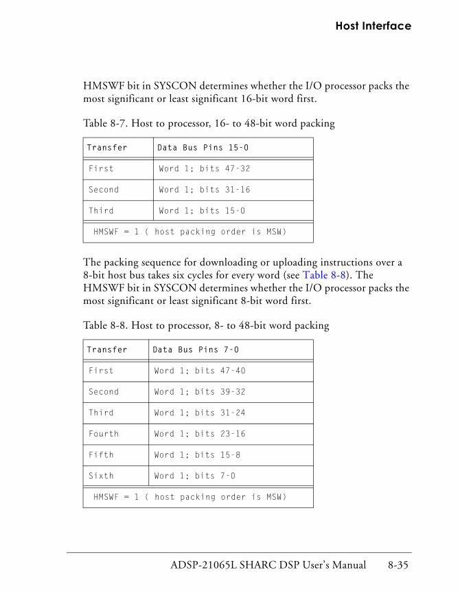
ADSP-21065L SHARC DSP User’s Manual 8-35
Host Interface
HMSWF bit in SYSCON determines whether the I/O processor packs the most significant or least significant 16-bit word first.
The packing sequence for downloading or uploading instructions over a 8-bit host bus takes six cycles for every word (see Table 8-8). The HMSWF bit in SYSCON determines whether the I/O processor packs the most significant or least significant 8-bit word first.
Table 8-7. Host to processor, 16- to 48-bit word packing
Transfer Data Bus Pins 15-0
First Word 1; bits 47-32
Second Word 1; bits 31-16
Third Word 1; bits 15-0
HMSWF = 1 ( host packing order is MSW)
Table 8-8. Host to processor, 8- to 48-bit word packing
Transfer Data Bus Pins 7-0
First Word 1; bits 47-40
Second Word 1; bits 39-32
Third Word 1; bits 31-24
Fourth Word 1; bits 23-16
Fifth Word 1; bits 15-8
Sixth Word 1; bits 7-0
HMSWF = 1 ( host packing order is MSW)

Interprocessor Messages
8-36 ADSP-21065L SHARC DSP User’s Manual
Interprocessor MessagesOnce granted control of the processor, the host can communicate with it by writing messages to its memory-mapped IOP registers. In a multipro-cessor system, the host can access the IOP registers of both processors.
The MSGR7-0 registers are general-purpose registers that you can use to pass messages between the host and the processor or to implement sema-phores and resource sharing between both processors.
You can use the MSGRx and VIRPT registers for message passing in the following ways:
• Message passing
The host can use any of the eight message registers, MSGR7-0, to communicate with the processor.
• Vector interrupts
The host can write the address of an interrupt service routine to the VIRPT register to issue a vector interrupt to the processor. This causes an immediate high-priority interrupt on the processor that, when serviced, causes the processor to branch to the specified service routine.
Since resources within a single processor can share these registers, conflicts can occur. Your system software is responsible for preventing such con-flicts. For details, see Appendix E, Control and Status Registers, in ADSP-21065L SHARC DSP Technical Reference.
The MSGRx and VIRPT registers also support shared-bus multiprocessing through the external port.
ADSP-21065L SHARC DSP User’s Manual 8-37
Host Interface
Message Passing (MSGRx)The host has three software protocols available to it for communicating with the processor through the processor’s MSGRx message registers:
• Vector-interrupt-driven
The host fills predetermined MSGRx registers with data and writes the address of the service routine to VIRPT to trigger a vector inter-rupt.
The service routine reads the data from the MSGRx registers and writes 0 to VIRPT to tell the host it is done. Alternatively, the service routine could signal the host using one of the processor’s FLAG3-0 pins.
• Register handshake
You designate four of the MSGRx registers as follows:
• A receive register (R)
• A receive handshake register (RH)
• A transmit register (T)
• A transmit handshake register (TH)
To pass data to the processor, the host writes data into T and then writes 1 into TH. When the processor sees 1 in TH, it reads the data from T and then writes 0 back to TH. When the host sees 0 in TH, it knows that the transfer has finished.
The processor follows the same sequence to pass data to the host through R and RH.

Interprocessor Messages
8-38 ADSP-21065L SHARC DSP User’s Manual
• Register write-back.
This method is similar to the register handshake method, but uses the T and R data registers only.
The host writes data to T. When the processor sees a non-zero value in T, it retrieves the value and writes 0 back to T.
The host uses a similar sequence to receive data.
This method works well only if the data to pass does not include 0.
Host Vector Interrupts (VIRPT)The processor uses vector interrupts to respond to interprocessor com-mands from the host or from another ADSP-21065L. When the host writes an address to the processor’s VIRPT register, it generates a vector interrupt.
When it services a vector interrupt, the processor automatically pushes the status stack and begins executing the service routine located at the address specified in VIRPT. The lower twenty-four bits of VIRPT contain the address. Optionally, you can use the upper eight bits as data for the inter-rupt service routine to read. At reset, the processor reinitializes VIRPT to its standard address in the interrupt vector table.
The minimum latency for vector interrupts is six cycles, five of which are NOPs. When the interrupt service routine reaches the RTI (return from interrupt) instruction, the processor automatically pops the status stack.
Make sure your system software checks the VIPD bit in the SYSTAT reg-ister. This bit reflects the status of the VIRPT register:
• If the host writes the VIRPT while a previous vector interrupt is pending, the new vector address replaces the pending one.
ADSP-21065L SHARC DSP User’s Manual 8-39
Host Interface
• If the host writes VIRPT while the processor is servicing an inter-rupt, the processor ignores the new vector address, so the host’s write doesn’t generate a new interrupt.
• A processor write to its own VIRPT register doesn’t generate an interrupt.
Using the processor’s vector interrupt feature, the host could perform the following procedure:
1. Poll the VIRPT register until it reads a certain token value (for example, 0).
2. Write the vector interrupt service routine address to VIRPT.
When the service routine is finished, the processor would write the token back to VIRPT to tell the host that it is finished.
3. Initiate another vector interrupt if necessary.

SYSTAT Register Bits
8-40 ADSP-21065L SHARC DSP User’s Manual
SYSTAT Register BitsThe SYSTAT register provides multiprocessing status information prima-rily. Figure 8-7 on page 8-43 shows the status bits in this register, and Table 8-9 describes them.
Table 8-9. SYSTAT status bits
Bit Name Description
0 HSTM Host mastership.
Indicates whether the host has been granted control of the bus.
0= Host is not bus master
1= Host is bus master
1 BSYN Bus synchronization.
Indicates when the processor’s bus arbitration logic is synchronized after reset. (See “Bus Arbitration Synchronization After Reset” on page 7-21 for detailed information.)
0= Bus arbitration logic is not synchronized
1= Bus arbitration logic is synchronized
2-3 Reserved
4-5 CRBM Current bus master.
ID2-0 of the current bus master.
If CRBM = ID of this processor, this processor is the current bus master.
CRBM is valid only for ID2-0> 0.
When ID2-0 = 000, CRBM is always 1.
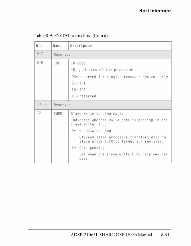
ADSP-21065L SHARC DSP User’s Manual 8-41
Host Interface
6-7 Reserved
8-9 IDC ID code.
ID1-0 pinouts of the processor.
00= reserved for single-processor systems only
01= ID1
10= ID2
11= reserved
10-11 Reserved
12 SWPD Slave write pending data.
Indicates whether valid data is pending in the slave write FIFO.
0= No data pending
Cleared after processor transfers data in slave write FIFO to target IOP register.
1= Data pending
Set when the slave write FIFO receives new data.
Table 8-9. SYSTAT status bits (Cont’d)
Bit Name Description

SYSTAT Register Bits
8-42 ADSP-21065L SHARC DSP User’s Manual
13 VIPD Vector interrupt pending.
Indicates that a pending vector interrupt has not yet been serviced.
0= No vector interrupt pending
Cleared on return from interrupt service routine.
1= Vector interrupt pending
Set when the VIRPT register has been writ-ten.
The host or other processor that issued the vector interrupt monitors this bit to determine when the service routine has finished and when it can issue a new vector interrupt.
14 HPS Host packing status.
Indicates whether host word packing has fin-ished or the stage packing is in. (For details, see “Data Packing” on page 8-24.)
0= Fully packed
1= Partially packed
15-31 Reserved
Table 8-9. SYSTAT status bits (Cont’d)
Bit Name Description

ADSP-21065L SHARC DSP User’s Manual 8-43
Host Interface
Figure 8-7. SYSTAT register bits
/()/
()/()
9 @-
.#7@A
$
$.
F -+
9+ E#
87- E
8- 7- E
+# C; ;
Interfacing with the System Bus
8-44 ADSP-21065L SHARC DSP User’s Manual
Interfacing with the System BusConsider a multiprocessor subsystem, consisting of two processors with local memory, as one of several processing elements connected together over a system bus. The ISA bus and the PCI bus are examples of such systems.
In these subsystems, the processing elements arbitrate through an arbitra-tion unit for control of the system bus. To arbitrate and become bus master, a device must be able to drive a bus request signal and respond to a bus grant signal. The arbitration unit, a device external to the processor, determines which request to grant in any given cycle.
Accessing the Cluster Bus and Slave ProcessorsFigure 8-8 on page 8-45 shows an example of a basic interface to a system bus that isolates the processor cluster bus from the system bus. The cluster bus connects two processors and an external memory device together.
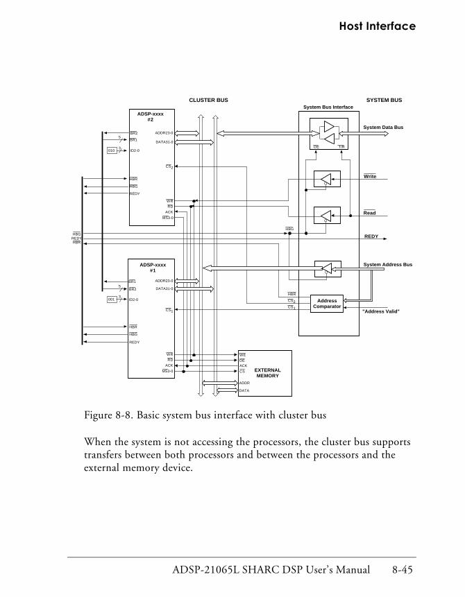
ADSP-21065L SHARC DSP User’s Manual 8-45
Host Interface
Figure 8-8. Basic system bus interface with cluster bus
When the system is not accessing the processors, the cluster bus supports transfers between both processors and between the processors and the external memory device.
ADSP-xxxx#1
ADDR23-0
DATA31-0
ID2-0
ADSP-xxxx#2
ADDR23-0
DATA31-0
ID2-0
WR
RD
ACK
MS3-0
HBR
HBG
BR2
BR1
001
010
5
3
3
5
HBR
HBG
WR
RD
ACK
MS3-0
ADDR
DATA
EXTERNALMEMORY
CS
ACKOE
WE
System Data Bus
REDY
REDY
Write
Read
System Address Bus
AddressComparator
CS1
HBG
HBR
CS2
CS2CS1
REDYHBGREDYHBR
System Bus Interface
OE T/R
CLUSTER BUS SYSTEM BUS
BR1
BR2
"Address Valid"

Interfacing with the System Bus
8-46 ADSP-21065L SHARC DSP User’s Manual
System accesses of the processors follow this procedure:
1. When the system wants to access a processor, it executes a read or write to the address range of the subsystem’s IOP registers.
2. The address comparator in the system bus interface detects a local access and asserts HBR and the CS line of the appropriate processor.
3. The selected processor holds off the system bus with REDY until it is ready to accept the data.
4. The master processor asserts the HBG signal.
HBG enables the system bus buffers, while the read and write sig-nals control the buffers’ direction for data.
To avoid glitches on the HBR line when addresses are changing, an address latch enable signal from the system or the system read or write sig-nals can qualify the address comparator. These methods cause the address comparator to deassert HBR each time the system deasserts a read or write or the address changes. Because these techniques deassert HBR with each access, the overhead of an HTC (Host Transition Cycle) occurs as part of each access. To avoid this type of overhead, latch HBG during long sequences of bus accesses.
Master Processor Accesses of the System BusFigure 8-9 on page 8-47 shows a more complex, bidirectional system interface in which a processor becomes bus master to access the system bus.

ADSP-21065L SHARC DSP User’s Manual 8-47
Host Interface
Figure 8-9. Bidirectional system bus interface
Before it begins the access, the processor generates the system bus request signal to request permission to become bus master. The system bus arbi-tration unit determines when to respond with the system bus grant signal on pin FLAG0.
The method a processor uses to arbitrate for the system bus depends on whether its core or its DMA controller initiates the access.
ADSP-xxxx#1
ADDR23-0
DATA23-0
ID2-0
ADSP-xxxx#2
ADDR23-0
DATA31-0
ID2-0
WR
RDACK
MS3-0
HBR
HBG
BR1
001
010
5
3
3
BR25
HBR
HBG
WR
RD
ACK
MS3-0
ADDR
DATA
EXTERNALMEMORY
CS
ACK
OE
WE
System Data Bus
REDY
REDY
Host Write
Host Read
System Address Bus
FLAG0
FLAG0
System Bus Grant
AddressComparator
CS1
SBTS
HBG
HBR
CS2
SBTS
CS2
CS1
REDYHBGREDYHBR
ACK
MS3-0
System Bus Request
System Bus Interface
WR
RD
HBG
"Address Valid"
BR1
BR2
CLUSTER BUS SYSTEM BUS

Interfacing with the System Bus
8-48 ADSP-21065L SHARC DSP User’s Manual
Core Accesses of the System Bus
The processor’s core uses one of two methods to access the system bus:
• The core sets a flag (FLAGx) and waits for the system bus grant sig-nal through another FLAG.
This method avoids tying up the local bus during the wait. Tying the system bus grant signal to an interrupt pin enables the proces-sor’s core to continue doing useful work while it waits.
• The processor’s core assumes that the system bus is available, and if it isn’t, the core either waits or aborts the access.
The processor asserts one of its memory select lines MS3-0 to begin the access. Doing so also asserts the system bus request signal. If the system bus is unavailable (FLAG0 is deasserted), the system bus interface asserts ACK to hold off the processor. Although this approach is simple, accesses to a busy system bus tie up both the processor and the cluster bus. To resolve this, you can use the Type 10 instruction (see page A-52, in ADSP-21065L SHARC DSP Tech-nical Reference):
IF condition JUMP(addr), ELSE compute, DM(addr) = dreg;
In this example, the Type 10 instruction aborts the bus access if the condition, the system bus grant signal (FLAG0), is false and causes a branch to a try again later routine. This method works well if the system bus grant signal (FLAG0) is asserted most of the time.
If you don’t use the Type 10 instruction and the processor’s core attempts an access before the bus has been granted, the access can cause a deadlock condition.
ADSP-21065L SHARC DSP User’s Manual 8-49
Host Interface
Resolving Bus Access Deadlock
It’s rare but possible for both the system and the processor to try to access each other’s bus in the same cycle, causing a deadlock in which ACK remains deasserted, so neither access can finish.
Normally, the master processor, in response to an HBR request, asserts HBG after the completion of the current access. If it is accessing the sys-tem bus at the same time, however, the master processor does not assert HBG because the current access cannot finish.
To break this type of deadlock, once your software detects it (both sides have enabled a system bus to cluster bus buffer), assert the SBTS (Suspend Bus Three-state pin) input for one or more cycles. (For details, see page 8-50.)
When the host asserts both SBTS and HBR, the processor enters slave mode and suspends its external access. This enables the system’s access to the cluster bus to proceed after the processor asserts HBG.
Apply the SBTS and HBR combination only when a processor’s access to the system bus causes a deadlock. Do not apply it during a cluster bus transfer because doing so causes two assertions of the WR signal, once before SBTS is asserted and once after the access resumes. With transfers between two processors over the cluster bus, this procedure violates the slave’s timing requirements.
Results of using the SBTS/HBR combination depend on the conditions under which it was applied:
• When the host asserts both SBTS and HBR in the same cycle that the processor is performing an external access, the external access is suspended until the host deasserts both SBTS and HBR.
• When the host asserts SBTS and HBR during an external DMA access, the processor does not assert HBG until the access has fin-ished.

Interfacing with the System Bus
8-50 ADSP-21065L SHARC DSP User’s Manual
• When the host asserts SBTS and HBR while bus lock is set, the pro-cessor places its bus signals in a high impedance state, but does not enter slave mode.
The host can suspend a processor’s access in progress and gain access to the processor’s internal resources, if:
• The access originates from the processor’s core, not its DMA con-troller;
• Bus lock is disabled.
To do so, the host performs this procedure:
1. After it asserts HBR, the host asserts SBTS for one or more cycles.
If SBTS is asserted one or more cycles after the processor recognizes HBR, the processor is guaranteed to assert HBG in the next cycle. The host must deassert SBTS between the time it receives HBG and the time it deasserts HBR.
2. The host drives both RD and WR strobes to their correct value (within the setup time specified in the processor’s data sheet) after the processor asserts HBG.
The host can then perform as many accesses as needed.
The host has full control of the bus and can access the other the processor or other peripherals on the bus.
3. The host deasserts HBR.
4. One cycle after deasserting HBG, the processor restarts its sus-pended access.
DMA Controller Accesses of the System Bus
Unlike with core accesses, with DMA controller accesses, you cannot use the SBTS and HBR combination to resolve a system bus deadlock because
ADSP-21065L SHARC DSP User’s Manual 8-51
Host Interface
once a DMA word transfer has begun in the processor, it must finish (the DMA controller must receive the ACK signal). If the host asserts SBTS and HBR during a DMA access, the master processor does not assert HBG until the access cycle has finished. Preventing the single DMA access from finishing can create a deadlock condition.
To prevent system bus deadlock when using DMA, your software must make sure that the system bus arbitration unit has asserted the system bus grant signal before it initiates the DMA sequence. If a higher priority access needs attention, to hold off the DMA sequence, the host can assert HBR at any time after a word has been transferred.
To prevent another deadlock, make sure the system bus arbitration unit asserts the system bus grant signal before the host deasserts HBR. When the DMA sequence finishes, make sure the DMA interrupt service routine clears the external system bus request flag.
Because the system bus is likely to be substantially slower than the proces-sor’s cluster bus, using DMA handshake mode may improve performance on the cluster bus. In this case, you tie the system bus grant signal to the DMA request line, DMARx. Then the DMA controller initiates access to the cluster bus and the system bus only when the system bus is available.
Using a FIFO in the system bus interface to post DMA data from the clus-ter bus may also increase performance on the cluster bus, offsetting a slow system bus.
Uniprocessor to Microprocessor Bus InterfaceOne processor without external memory can connect more or less directly to a host’s bus, requiring few or no buffers. This type of connection assumes that the processor can execute its application from internal mem-ory most of the time, with only occasional need to request an external access.

Interfacing with the System Bus
8-52 ADSP-21065L SHARC DSP User’s Manual
In this configuration, the host continuously asserts HBR, unless it detects BR1 (the BRx line of the processor with ID1). Then, when the host is ready to give up its bus, it deasserts HBR to enable the processor to per-form an external access.
Most of the time, however, the host can read or write to the processor at will. To do so, the host asserts CS and initiates handshaking with REDY. In this scenario, the processor need not respond with HBG.
ADSP-21065L SHARC DSP User’s Manual 9-1
9 SERIAL PORTSFigure 9-0.
Table 9-0.
Listing 9-0.
The processor has two independent, synchronous serial ports, SPORT0 and SPORT1, that provide an I/O interface to peripheral devices.
Each serial port has a set of control registers and data buffers. With a range of clock and frame synchronization options, the SPORTs support a variety of serial communication protocols and provide a glueless hardware inter-face to industry-standard data converters and CODECs.
The processor’s serial ports provide these features and capabilities:
• Two transmit and two receive channels per serial port.
Each serial port can transmit and receive data simultaneously for full duplex operation.
• Inexpensive eight- or six-line connection to peripheral devices for two-way communication.
• Independent transmit and receive functions.
Independent functioning provides greater flexibility for serial com-munications.
• Double buffering of data.
• Integral hardware for µ-law and A-law companding.
• Operation at processor’s full clock rate.
This capability provides each with a maximum data rate ofnM bit/s, where n equals the processor’s input clock frequency.

9-2 ADSP-21065L SHARC DSP User’s Manual
• Core controlled interrupt-driven, single-word transfers to and from on-chip memory.
• DMA controller controlled block transfers to and from on-chip memory, including chained DMA operations of multiple data blocks.
• Three operation modes: standard, I2S, and multichannel.
In standard mode, one or both transmit channels can transmit, and one or both receive channels can receive.
In I2S mode, one or both transmit channels can transmit, and one or both receive channels can receive. Each channel either transmits or receives L and R channels.
In both standard and I2S modes, when both A and B channels are used, they transmit or receive data simultaneously, sending or receiving bit 0 on the same edge of the serial clock, bit 1 on the next edge of the serial clock, and so on.
In multichannel mode, each SPORT can receive and transmit data selectively from channels of a time-division-multiplexed serial bit-stream—a useful option for T1 interfaces.
• Support for internally or externally generated serial clock and frame sync signals in a wide range of frequencies.
• Support for data words of 3- to 32-bits and MSB or LSB formats.

ADSP-21065L SHARC DSP User’s Manual 9-3
Serial Ports
Figure 9-1. Serial port block diagram
HardwareCompanding
(compression)
DM Data busPM Data busI/O Data bus
32
32 32
32 32
32 32
32 32
Tx0_ATransmit Data Buffer
Tx0_BTransmit Data Buffer
Rx0_AReceive Data Buffer
Rx0_BReceive Data Buffer
HardwareCompanding(expansion)
Transmit ShiftRegister
Transmit ShiftRegister
Receive ShiftRegister
Receive ShiftRegister
Serial PortControl
DT0A DR0ADT0B DR0B
TCLKn RCLKnTFSn
TFSn
RFSn
RFSn

Serial Port Connections
9-4 ADSP-21065L SHARC DSP User’s Manual
Serial Port ConnectionsFigure 9-1 on page 9-3 shows the architecture of each serial port and Table 9-1 lists and describes the pins.
A serial port receives serial data on its DR input and transmits serial data on its DT output. It can receive and transmit simultaneously for full duplex operation.
Serial communications are synchronized to a clock signal—a clock pulse must accompany every data bit. Each serial port can generate or receive its
Table 9-1. Serial port pins
Function
SPORT0 SPORT1
A Chn B Chn A Chn B Chn
Transmit data DT0A DT0B DT1A DT1B
Transmit clock TCLK0 TCLK1
Transmit frame sync/word select
TFS0 TFS1
Receive data DR0A DR0B DR1A DR1B
Receive clock RCLK0 RCLK1
Receive frame sync RFS0 RFS1
For non-multichannel mode the processor drives the DT pins only when actively transmitting data, (that is, a frame sync has been rec-ognized and data has not finished transmitting). Otherwise, they are three-stated. In multichannel mode, DT is driven if the transmitter is active in that time slot. Otherwise, it is in a high impedance state (if it is in an inactive slot).

ADSP-21065L SHARC DSP User’s Manual 9-5
Serial Ports
own transmit clock signal (TCLK) and receive clock signal (RCLK). You configure internally-generated serial clock frequencies in a serial port’s TDIVx and RDIVx registers.
You can use frame synchronization to signal data, signaling either at the beginning of an individual word or at the beginning of a block of words. Configuration of the frame sync signals depends on the type of serial device connected to the processor. Each serial port can generate or receive its own transmit frame sync (TFS) signal and receive frame sync (RFS) sig-nal. You configure internally-generated frame sync frequencies in a serial port’s TDIVx and RDIVx registers.
Figure 9-1 on page 9-3 shows the components of a serial port. The proces-sor’s core writes data for transmission to the TX buffer. Serial port hardware compresses (optional) the data, then automatically transfers it to the transmit shift register. The transmit shift register shifts the data out on the SPORT’s DT pin synchronously to the TCLK transmit clock. When using framing signals, the TFS signal indicates the beginning of the serial word transmission. With serial port enabled (SPEN=1), the processor always drives the DT pin, unless the channel is operating in multichannel mode and an inactive time slot occurs. (For details, see “Multichannel Mode” on page 9-67.)
Likewise, the receive shift register shifts in data from the SPORT’s DR pin synchronously to the RCLK receive clock. When using framing signals, the RFS signal indicates the beginning of the serial word reception. When the receive shift register shifts in an entire word, serial port hardware expands (optional) the data, then automatically transfers it to the RX buffer.
Because the processor’s SPORTs are not UARTs, they cannot communicate with an RS-232 device or with any other asyn-chronous communications protocol.
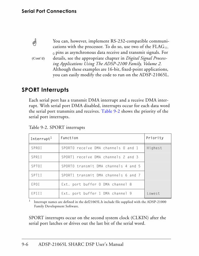
Serial Port Connections
9-6 ADSP-21065L SHARC DSP User’s Manual
SPORT InterruptsEach serial port has a transmit DMA interrupt and a receive DMA inter-rupt. With serial port DMA disabled, interrupts occur for each data word the serial port transmits and receives. Table 9-2 shows the priority of the serial port interrupts.
SPORT interrupts occur on the second system clock (CLKIN) after the serial port latches or drives out the last bit of the serial word.
(Cont’d)
You can, however, implement RS-232-compatible communi-cations with the processor. To do so, use two of the FLAG11-
0 pins as asynchronous data receive and transmit signals. For details, see the appropriate chapter in Digital Signal Process-ing Applications Using The ADSP-2100 Family, Volume 2. Although these examples are 16-bit, fixed-point applications, you can easily modify the code to run on the ADSP-21065L.
Table 9-2. SPORT interrupts
Interrupt1
1 Interrupt names are defined in the def21065L.h include file supplied with the ADSP-21000 Family Development Software.
Function Priority
SPR0I SPORT0 receive DMA channels 0 and 1 Highest
SPR1I SPORT1 receive DMA channels 2 and 3
SPT0I SPORT0 transmit DMA channels 4 and 5
SPT1I SPORT1 transmit DMA channels 6 and 7
EP0I Ext. port buffer 0 DMA channel 8
EP1II Ext. port buffer 1 DMA channel 9 Lowest
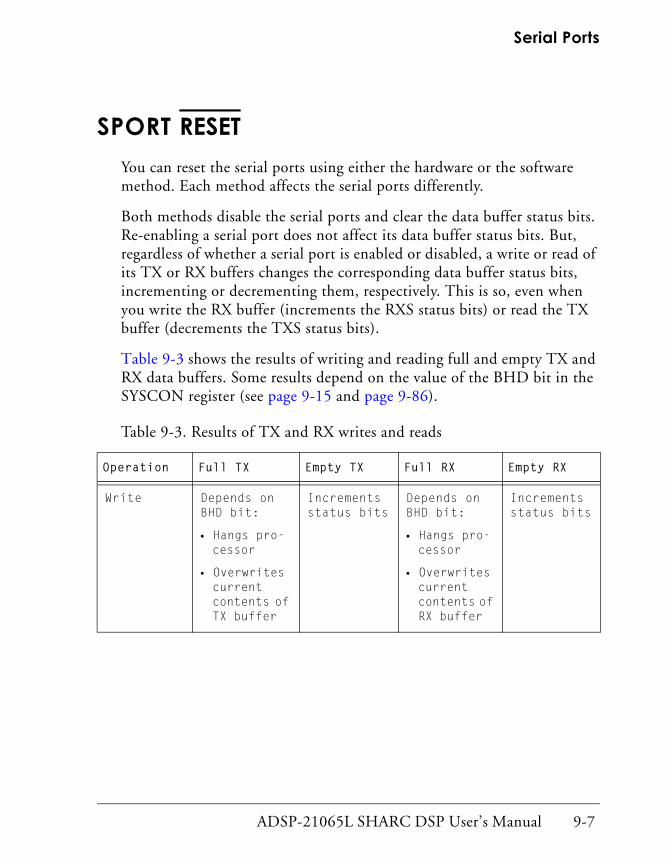
ADSP-21065L SHARC DSP User’s Manual 9-7
Serial Ports
SPORT RESETYou can reset the serial ports using either the hardware or the software method. Each method affects the serial ports differently.
Both methods disable the serial ports and clear the data buffer status bits. Re-enabling a serial port does not affect its data buffer status bits. But, regardless of whether a serial port is enabled or disabled, a write or read of its TX or RX buffers changes the corresponding data buffer status bits, incrementing or decrementing them, respectively. This is so, even when you write the RX buffer (increments the RXS status bits) or read the TX buffer (decrements the TXS status bits).
Table 9-3 shows the results of writing and reading full and empty TX and RX data buffers. Some results depend on the value of the BHD bit in the SYSCON register (see page 9-15 and page 9-86).
Table 9-3. Results of TX and RX writes and reads
Operation Full TX Empty TX Full RX Empty RX
Write Depends on BHD bit:
• Hangs pro-cessor
• Overwrites current contents of TX buffer
Increments status bits
Depends on BHD bit:
• Hangs pro-cessor
• Overwrites current contents of RX buffer
Increments status bits
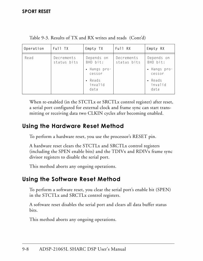
SPORT RESET
9-8 ADSP-21065L SHARC DSP User’s Manual
When re-enabled (in the STCTLx or SRCTLx control register) after reset, a serial port configured for external clock and frame sync can start trans-mitting or receiving data two CLKIN cycles after becoming enabled.
Using the Hardware Reset MethodTo perform a hardware reset, you use the processor’s RESET pin.
A hardware reset clears the STCTLx and SRCTLx control registers (including the SPEN enable bits) and the TDIVx and RDIVx frame sync divisor registers to disable the serial port.
This method aborts any ongoing operations.
Using the Software Reset MethodTo perform a software reset, you clear the serial port’s enable bit (SPEN) in the STCTLx and SRCTLx control registers.
A software reset disables the serial port and clears all data buffer status bits.
This method aborts any ongoing operations.
Read Decrements status bits
Depends on BHD bit:
• Hangs pro-cessor
• Reads invalid data
Decrements status bits
Depends on BHD bit:
• Hangs pro-cessor
• Reads invalid data
Table 9-3. Results of TX and RX writes and reads (Cont’d)
Operation Full TX Empty TX Full RX Empty RX

ADSP-21065L SHARC DSP User’s Manual 9-9
Serial Ports
SPORT Control Registers and Data BuffersEach SPORT has a set of control and configuration registers and data buffers, as shown in Table 9-4. These registers and buffers are part of the IOP register set.
Table 9-4. SPORT control and data registers
Register Function
STCTLx SPORT transmit control register
TXx_z1
1 x = Serial port 0 or 1; z = Channel A or B
Transmit data buffer
TDIVx Transmit clock and frame sync divisors
MTCSx Multichannel transmit select
MTCCSx Multichannel transmit compand select
SRCTLx SPORT receive control register
RXx_z1 Receive data buffer
RDIVx Receive clock and frame sync divisors
MRCSx Multichannel receive select
MRCCSx Multichannel receive companding select
KEYWDx SPORT receive comparison register
IMASKx SPORT receive comparison mask

SPORT Control Registers and Data Buffers
9-10 ADSP-21065L SHARC DSP User’s Manual
Table 9-5 shows the memory-mapped address and reset initialization value of each SPORT register. All of these registers are 32 bits wide.
Table 9-5. SPORT registers memory-mapped addresses and reset values
Register Address Reset Description
STCTL0 0x00E0 0x0000 0000 SPORT0 transmit control reg-ister
SRCTL0 0x00E1 0x0000 0000 SPORT0 receive control reg-ister
TX0_A 0x00E2 None SPORT0 transmit data buffer;A data
RX0_A 0x00E3 None SPORT0 receive data buffer; A data
TDIV0 0x00E4 None SPORT0 transmit divisor
Reserved 0x00E5
RDIV0 0x00E6 None SPORT0 receive divisor
Reserved 0x00E7
MTCS0 0x00E8 None SPORT0 multichannel transmit select
MRCS0 0x00E9 None SPORT0 multichannel receive select
MTCCS0 0x00EA None SPORT0 multichannel transmit compand select
MRCCS0 0x00EB None SPORT0 multichannel receive compand select
KEYWD0 0x00EC None SPORT0 receive comparison register

ADSP-21065L SHARC DSP User’s Manual 9-11
Serial Ports
IMASK0 0x00ED None SPORT0 receive comparison mask register
TX0_B 0x00EE None SPORT0 transmit data buffer;B data
RX0_B 0x00EF None SPORT0 receive data buffer; B data
STCTL1 0x00F0 0x0000 0000 SPORT1 transmit control reg-ister
SRCTL1 0x00F1 0x0000 0000 SPORT1 receive control reg-ister
TX1_A 0x00F2 None SPORT1 transmit data buffer;A data
RX1_A 0x00F3 None SPORT1 receive data buffer; A data
TDIV1 0x00F4 None SPORT1 transmit divisor
Reserved 0x00F5
RDIV1 0x00F6 None SPORT1 receive divisor
Reserved 0x00F7
MTCS1 0x00F8 None SPORT1 multichannel transmit select
MRCS1 0x00F9 None SPORT1 multichannel receive select
MTCCS1 0x00FA None SPORT1 multichannel transmit compand select
Table 9-5. SPORT registers memory-mapped addresses and reset values
Register Address Reset Description

SPORT Control Registers and Data Buffers
9-12 ADSP-21065L SHARC DSP User’s Manual
To program the SPORT control registers, you write to the appropriate address in memory. Applications can use the symbolic names of the regis-ters and individual control bits. The file def21065L.h, provided in the INCLUDE directory of the ADSP-21000 Family Development Software, con-tains the #define definitions for these symbols. See Appendix E, Control and Status Registers, in ADSP-21065L SHARC DSP Technical Reference, for a listing of the file’s contents.
All control and status bits in the SPORT registers are active high unless otherwise noted.
Because the SPORT registers are memory-mapped, you cannot write them with data coming directly from memory. Instead, you must write or read them from or to the processor’s core registers, usually one of the Register File’s general-purpose universal registers (R15–R0).
External devices, such as another ADSP-21065L or a host, can write and read the SPORT control registers to set up a serial port DMA operation, for example.
MRCCS1 0x00FB None SPORT1 multichannel receive compand select
KEYWD1 0x00FC None SPORT1 receive comparison register
IMASK1 0x00FD None SPORT1 receive comparison mask register
TX1_B 0x00FE None SPORT1 transmit data buffer;B data
RX1_B 0x00FF None SPORT1 receive data buffer; B data
Table 9-5. SPORT registers memory-mapped addresses and reset values
Register Address Reset Description

ADSP-21065L SHARC DSP User’s Manual 9-13
Serial Ports
When changing operating modes, write the serial port’s control register, STCTLx or SRCTLx, with all 0s to clear it before you write the new mode to the register.
Register Writes and Effect LatencyThe processor completes internal writes to SPORT registers at the end of the same CLKIN cycle in which they begin. So the newly written value is available in the register on the next cycle. But when a write to one of the STCTLx or SRCTLx control registers immediately follows a read of the same register, the write takes at least two cycles to finish.
After a write to a SPORT register, control and mode bit changes take effect by the end of the second CLKIN cycle after the write has finished. Two CLKIN cycles after they are enabled (in the STCTLx or SRCTLx reg-ister), the serial ports can start transmitting or receiving, losing no serial clock cycles from that point on.
Transmit and Receive Data Buffers (TX, RX)TX0_A and TX0_B are the transmit data buffers for SPORT0, and TX1_A and TX1_B are the transmit data buffers for SPORT1. Either the DMA controller or the processor’s core program must load these 32-bit buffers with the data to transmit.
RX0_A and RX0_B are the receive data buffers for SPORT0, and RX1_A and RX1_B are the receive data buffers for SPORT1. The receive shift reg-ister automatically loads these 32-bit buffers when the serial port has received an entire word. The receive and transmit buffers right-justify words containing less than thirty-two bits.
TX Buffer Operation
Because they have a data register and an output shift register, the TX buff-ers behave like two-location FIFOs (see Figure 9-1 on page 9-3).
SPORT Control Registers and Data Buffers
9-14 ADSP-21065L SHARC DSP User’s Manual
You can store only two 32-bit words in a TX buffer at a time. When the TX buffer is loaded and the serial port has transmitted the previous word, the TX buffer automatically loads its contents into the transmit shift regis-ter. This transfer generates an interrupt, signaling that the TX buffer is not full and ready to accept the next word. When serial port DMA is enabled or the corresponding mask bit in the IMASK register is set, this interrupt does not occur.
When a transmit frame synch occurs and the TX buffer contains no new data, the processor sets the transmit underflow status bit (TUVF) in the transmit control register. The TUVF status bit is sticky (the application must explicitly clear the bit), and you must disable the serial port to clear it.
RX Buffer Operation
Because they have two data register and an input shift register, the RX buffers behave like three-location FIFOs (see Figure 9-1 on page 9-3).
You can store two 32-bit words in an RX buffer while the receive shift reg-ister is shifting in a third word. The third word overwrites the second if the processor’s core or the DMA controller has not read the first word. When this occurs, the processor sets the receive overflow status bit (ROVF) in the receive control register. The RX buffer can receive almost three entire words without an internal read before overflow occurs. The processor generates the overflow status on the last bit of third word. The ROVF status bit is sticky, and you must disable the serial port to clear it.
When the RX buffer has received a word (the buffer is not empty), it gener-ates an interrupt. When serial port DMA is enabled or the corresponding bit in the IMASK register is set, the processor masks this interrupt.
Reading and Writing RX, TX
If the processor’s core attempts to read from an empty RX buffer or to write to a full TX buffer, the processor delays the access until the external

ADSP-21065L SHARC DSP User’s Manual 9-15
Serial Ports
I/O device accesses the buffer. This delay is called a core processor hang. To avoid hanging the processor’s core, read the buffer’s full or empty status (in STCTLx or SRCTLx) before accessing a TX or RX buffer. To prevent this type of hang condition globally, set the BHD (Buffer Hang Disable) bit in the SYSCON register (see Table 9-3 on page 9-7).
The processor updates the status bits in STCTLx and SRCTLx during core reads and writes, even when the serial port is disabled. For details, see page 9-7.
Make sure your application disables a serial port when it writes to the serial port’s RX buffer or reads from the serial port’s TX buffer; for exam-ple, if it tests the results of companding.
Transmit and Receive Control Registers(STCTL, SRCTL)
The main control registers for each serial port are the transmit control reg-ister, STCTLx, and the receive control register, SRCTLx. See Table 9-6 and Table 9-7 on page 9-21 for the bit definitions of these registers. For default bit values, see Figure 9-2 on page 9-18, Figure 9-3 on page 9-19, Figure 9-4 on page 9-20, Figure 9-5 on page 9-23, Figure 9-6 on page 9-24, and Figure 9-7 on page 9-25. Some bit definitions depend on the mode of operation for which the serial port is configured.
Table 9-6. STCTLx transmit control bits
Bit I2S Mode Standard Mode Multichannel Mode
0 SPEN_A SPEN_A Reserved
1 Reserved DTYPE DTYPE
2 Reserved DTYPE DTYPE
3 Reserved SENDN SENDN

SPORT Control Registers and Data Buffers
9-16 ADSP-21065L SHARC DSP User’s Manual
4 SLEN0 SLEN0 SLEN0
5 SLEN1 SLEN1 SLEN1
6 SLEN2 SLEN2 SLEN2
7 SLEN3 SLEN3 SLEN3
8 SLEN4 SLEN4 SLEN4
9 PACK PACK PACK
10 MSTR ICLK Reserved
11 OPMODE OPMODE OPMODE
12 Reserved CKRE CKRE
13 Reserved TFSR Reserved
14 Reserved ITFS Reserved
15 DITFS DITFS DITFS
16 L_FIRST LTFS LTFS
17 Reserved LAFS Reserved
18 SDEN_A SDEN_A SDEN_A
19 SCHEN_A SCHEN_A SCHEN_A
20 SDEN_B SDEN_B MFD
21 SCHEN_B SCHEN_B MFD
Table 9-6. STCTLx transmit control bits (Cont’d)
Bit I2S Mode Standard Mode Multichannel Mode
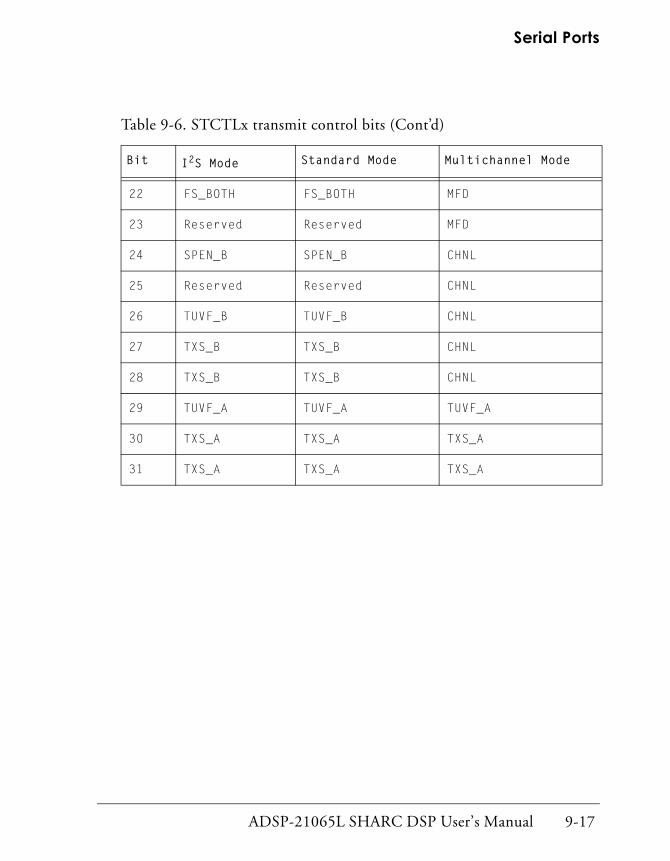
ADSP-21065L SHARC DSP User’s Manual 9-17
Serial Ports
22 FS_BOTH FS_BOTH MFD
23 Reserved Reserved MFD
24 SPEN_B SPEN_B CHNL
25 Reserved Reserved CHNL
26 TUVF_B TUVF_B CHNL
27 TXS_B TXS_B CHNL
28 TXS_B TXS_B CHNL
29 TUVF_A TUVF_A TUVF_A
30 TXS_A TXS_A TXS_A
31 TXS_A TXS_A TXS_A
Table 9-6. STCTLx transmit control bits (Cont’d)
Bit I2S Mode Standard Mode Multichannel Mode

SPORT Control Registers and Data Buffers
9-18 ADSP-21065L SHARC DSP User’s Manual
Figure 9-2. STCTLx transmit control register—Standard mode
31 30 29 28 27 26 25 24 23 22 21 20 19 18 17 16
0 0 00000 00000000 0
15 14 13 12 11 10 9 8 7 6 5 4 3 2 1 0
0 0 00000 00000000 0
OPMODEOperation Mode
0=non-I2S mode1=I2S mode
DITFSTFS Data
Dependency0=depend.
1=independ.
SLENSerial Word Length -1
SPEN_ASPORT Enable A0=disable1=enable
PACK16/32-bit pack0=no pack1=pack
ITFSTFS Source
0=external1=internal
LTFSActive Low TFS0=active high1=active low
SDEN_ASPORT xmit DMA enable A0=disable1=enable
TXS_AStatus *
TX A Data Buffer00=empty
10=partially full11=full
TUVF_AStatus * (sticky)TX A Underflow
SCHEN_ASPORT xmit DMA chaining enable A0=disable1=enableSDEN_B
SCHEN_B
FS_BOTHWord Select
0=issue if data in either Tx
1=issue only if data in both Tx
TXS_B *
TUVF_B *
SPEN_BSPORT Enable B
0=disable1=enable
* Status is read-only
LAFSLate TFS0=early1=late
TFSRTFS Requirement
0=no TFS required1=TFS required CKRE
Active Clock Edge0=falling edge1=rising edge
ICLKXmit Clk Source0=external1=internal
SENDNEndian word format0=MSB first1=LSB first
DTYPEData Type00=r-justify; fill MSB w/0s01=r-justify; sign-ext MSB10=compand µ-law11=compand A-law

ADSP-21065L SHARC DSP User’s Manual 9-19
Serial Ports
Figure 9-3. STCTLx transmit control register—I2S mode
31 30 29 28 27 26 25 24 23 22 21 20 19 18 17 16
0 0 00000 00000000 0
15 14 13 12 11 10 9 8 7 6 5 4 3 2 1 0
0 0 00000 00000000 0
OPMODEOperation Mode
0=non-I2S mode1=I2S mode
DITFSData Dependency TFS0=data dependent1=data independent
SLENSerial Word Length -1
SPEN_ASPORT Enable A0=disable1=enable
PACK16/32-bit packing0=no pack1=pack
MSTRMaster/Slave mode0=TX is slave1=TX is master
L_FIRSTXmit left chn. first0=right chn. first1=left chn. first
SDEN_ASPORT DMA enable A0=disable1=enable
TXS_AStatus *TX A Data Buffer00=empty10=partially full11=full
TUVF_AStatus * (sticky)TX A Underflow
SCHEN_ASPORT xmit DMA chaining enable A0=disable1=enable
SDEN_B
SCHEN_B
FS_BOTHWord Select0=issue if data in either Tx1=issue only if data in both Tx
TXS_B *
TUVF_B *
SPEN_BSPORT Enable B0=disable1=enable
* Status is read-only

SPORT Control Registers and Data Buffers
9-20 ADSP-21065L SHARC DSP User’s Manual
Figure 9-4. STCTLx transmit control register—multichannel mode
31 30 29 28 27 26 25 24 23 22 21 20 19 18 17 16
0 0 00000 00000000 0
SDEN_ASPORT xmit DMA enable A0=disable1=enable
TXS_AStatus *TX A Data Buffer00=empty10=partially full11=full
TUVF_AStatus * (sticky)TX A Underflow
SCHEN_ASPORT xmit DMA chaining enable A0=disable1=enable
MFDMultichn Frame Delay
CHNL*Currently Selected Chn
* Status is read-only
LTFSActive State TFS0=active high1=active low
15 14 13 12 11 10 9 8 7 6 5 4 3 2 1 0
0 0 00000 00000000 0
OPMODEOperation Mode
0=non-I2S mode1=I2S mode
DITFSTFS Data Dependency0=depend.1=independ.
SLENSerial Word Length -1
PACK16/32-bit pack0=no pack1=pack
CKREActive Clock Edge0=falling edge1=rising edge
SENDNEndian word format0=MSB first1=LSB first
DTYPEData Typex0=r-justify; fill MSB w/0sx1=r-justify; sign-ext MSB0x=compand µ-law1x=compand A-law
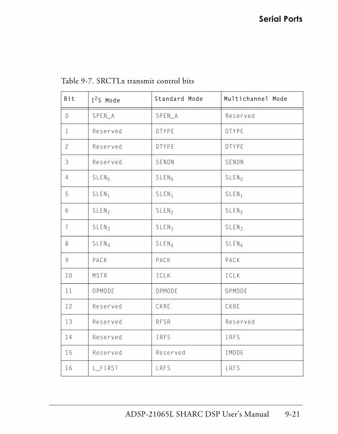
ADSP-21065L SHARC DSP User’s Manual 9-21
Serial Ports
Table 9-7. SRCTLx transmit control bits
Bit I2S Mode Standard Mode Multichannel Mode
0 SPEN_A SPEN_A Reserved
1 Reserved DTYPE DTYPE
2 Reserved DTYPE DTYPE
3 Reserved SENDN SENDN
4 SLEN0 SLEN0 SLEN0
5 SLEN1 SLEN1 SLEN1
6 SLEN2 SLEN2 SLEN2
7 SLEN3 SLEN3 SLEN3
8 SLEN4 SLEN4 SLEN4
9 PACK PACK PACK
10 MSTR ICLK ICLK
11 OPMODE OPMODE OPMODE
12 Reserved CKRE CKRE
13 Reserved RFSR Reserved
14 Reserved IRFS IRFS
15 Reserved Reserved IMODE
16 L_FIRST LRFS LRFS

SPORT Control Registers and Data Buffers
9-22 ADSP-21065L SHARC DSP User’s Manual
17 Reserved LAFS Reserved
18 SDEN_A SDEN_A SDEN_A
19 SCHEN_A SCHEN_A SCHEN_A
20 SDEN_B SDEN_B IMAT
21 SCHEN_B SCHEN_B Reserved
22 SPL SPL Reserved
23 Reserved MCE MCE
24 SPEN_B SPEN_B NCH
25 Reserved Reserved NCH
26 ROVF_B ROVF_B NCH
27 RXS_B RXS_B NCH
28 RXS_B RXS_B NCH
29 ROVF_A ROVF_A ROVF_A
30 RXS_A RXS_A RXS_A
31 RXS_A RXS_A RXS_A
Table 9-7. SRCTLx transmit control bits (Cont’d)
Bit I2S Mode Standard Mode Multichannel Mode
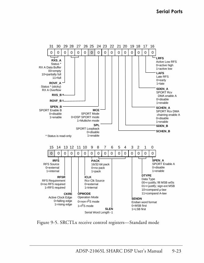
ADSP-21065L SHARC DSP User’s Manual 9-23
Serial Ports
Figure 9-5. SRCTLx receive control registers—Standard mode
31 30 29 28 27 26 25 24 23 22 21 20 19 18 17 16
0 0 00000 00000000 0
15 14 13 12 11 10 9 8 7 6 5 4 3 2 1 0
0 0 00000 00000000 0
OPMODEOperation Mode
0=non-I2S mode1=I2S mode
SLENSerial Word Length -1
SPEN_ASPORT Enable A0=disable1=enable
PACK16/32-bit pack0=no pack1=pack
IRFSRFS Source
0=external1=internal
LRFSActive Low RFS0=active high1=active low
SDEN_ASPORT Rcv DMA enable A0=disable1=enable
RXS_AStatus *
RX A Data Buffer00=empty
10=partially full11=full
ROVF_AStatus * (sticky)RX A Overflow
SCHEN_ASPORT Rcv DMA chaining enable A0=disable1=enableSDEN_B
SCHEN_B
SPLSPORT Loopback
0=disable1=enable
RXS_B *
ROVF_B *
SPEN_BSPORT Enable B
0=disable1=enable
* Status is read-only
LAFSLate RFS0=early1=late
RFSRRFS Requirement
0=no RFS required1=RFS required
CKREActive Clock Edge
0=falling edge1=rising edge
ICLKRcv Clk Source0=external1=internal
SENDNEndian word format0=MSB first1=LSB first
DTYPEData Type00=r-justify; fill MSB w/0s01=r-justify; sign-ext MSB10=compand µ-law11=compand A-law
MCESPORT Mode
0=DSP SPORT mode1=Multichn mode
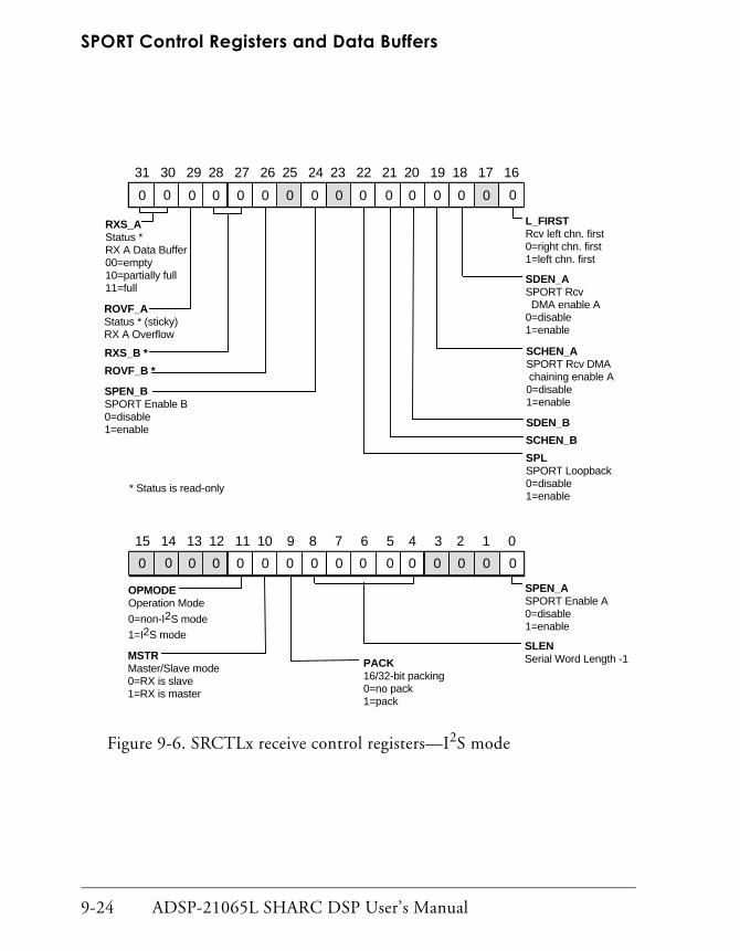
SPORT Control Registers and Data Buffers
9-24 ADSP-21065L SHARC DSP User’s Manual
Figure 9-6. SRCTLx receive control registers—I2S mode
31 30 29 28 27 26 25 24 23 22 21 20 19 18 17 16
0 0 00000 00000000 0
15 14 13 12 11 10 9 8 7 6 5 4 3 2 1 0
0 0 00000 00000000 0
OPMODEOperation Mode
0=non-I2S mode1=I2S mode
SLENSerial Word Length -1
SPEN_ASPORT Enable A0=disable1=enable
PACK16/32-bit packing0=no pack1=pack
MSTRMaster/Slave mode0=RX is slave1=RX is master
L_FIRSTRcv left chn. first0=right chn. first1=left chn. first
SDEN_ASPORT Rcv DMA enable A0=disable1=enable
RXS_AStatus *RX A Data Buffer00=empty10=partially full11=full
ROVF_AStatus * (sticky)RX A Overflow
SCHEN_ASPORT Rcv DMA chaining enable A0=disable1=enable
SDEN_B
SCHEN_B
SPLSPORT Loopback0=disable1=enable
RXS_B *
ROVF_B *
SPEN_BSPORT Enable B0=disable1=enable
* Status is read-only

ADSP-21065L SHARC DSP User’s Manual 9-25
Serial Ports
Figure 9-7. SRCTLx receive control registers—multichannel mode
31 30 29 28 27 26 25 24 23 22 21 20 19 18 17 16
0 0 00000 00000000 0
SDEN_ASPORT rcv DMA enable A0=disable1=enable
RXS_AStatus *
RX A Data Buffer00=empty
10=partially full11=full
ROVF_AStatus * (sticky)RX A Underflow
SCHEN_ASPORT rcv DMA chaining enable A0=disable1=enable
MCESPORT Mode
0=DSP SPORT mode1=Multichn Mode
NCHNumber of Chns -1
* Status is read-only
LRFSActive StateRFS0=active high1=active low
15 14 13 12 11 10 9 8 7 6 5 4 3 2 1 0
0 0 00000 00000000 0
OPMODEOperation Mode
0=non-I2S mode1=I2S mode
IMODERcv Compare
0=disable1=enable
SLENSerial Word Length -1
PACK16/32-bit pack0=no pack1=pack
CKREActive Clock Edge
0=falling edge1=rising edge
SENDNEndian word format0=MSB first1=LSB first
DTYPEData Typex0=r-justify; fill MSB w/0sx1=r-justify; sign-ext MSB0x=compand µ-law1x=compand A-lawICLK
Rcv Clk Source0=external1=internal
IMATRcv Compare Data
0=accept if false1=accept if true
IRFSRFS Source
0=external1=internal
SPORT Control Registers and Data Buffers
9-26 ADSP-21065L SHARC DSP User’s Manual
Bit definitions of the STCTLx and SRCTLx control register parameters are:
CHNLCurrent channel selected.
Multichannel mode only. STCTLx register.
Read-only, sticky status bits.
Identifies the currently selected transmit channel slot (0 to 31).
CKREFrame sync clock edge.
Standard and multichannel modes only. STCTLx and SRCTLx registers.
Selects the active edge of the serial port clock on which to sample or drive data and frame syncs.
In standard mode only, you can set this parameter separately for transmit and receive channels.
0 = Falling edge
1 = Rising edge
(Frame sync is level-sensitive, not edge-sensitive.)
DITFSData independent TFS.
All operation modes. STCTLx register.
Selects when the processor generates the transmit frame sync signal.

ADSP-21065L SHARC DSP User’s Manual 9-27
Serial Ports
0 = Data dependent TFS.
TFS signal generated only when new data is in SPORT chan-nel’s transmit data buffer and TDIV period occurs as programmed in the TDIV register.
1 = Data independent TFS.
TFS signal generated regardless of the validity of the data present in SPORT channel’s transmit data buffer. The proces-sor generates the TFS signal at the frequency specified by the value you load in the TDIV register.
DTYPEData type.
Standard and multichannel modes only. STCTLx and SRCTLx registers.
Selects the companding and MSB format of serial words loaded into the TX and RX buffers. (The transmit shift register does not 0-fill or sign-extend TX data words.)
Selection differs between modes.
For standard mode, selection of companding mode and MSB for-mat are exclusive:
00 =Right justify; fill unused MSBs with 0s.
01 =Right justify; sign-extend into unused MSBs.
10 =Compand using µ_law. (Primary channels only)
11 =Compand using A_law. (Primary channels only)
For multichannel mode, selection of companding mode and MSB format are independent:

SPORT Control Registers and Data Buffers
9-28 ADSP-21065L SHARC DSP User’s Manual
x0 =Right justify; fill unused MSBs with 0s.
x1 =Right justify; sign-extend into unused MSBs.
0x =Compand using µ_law.
1x =Compand using A_law.
FS_BOTHFrame sync both.
I2S and standard modes only. STCTLx register.
Selects when during transmission to issue the word select.
0 = Issue word select if data in either transmit channel.
1 = Issue word select only if data in both transmit channels.
ICLK Transmit and receive clock sources.
Standard and multichannel modes only. STCTLx and SRCTLx registers.
Selects the clock source to use to transmit and to receive data. In standard mode only, you can set this parameter separately for trans-mit and receive channels.
0 = Use an external clock.
1 = Use processor’s internal clock.
IMAT Receive comparison accept data.
Multichannel mode only. SRCTLx register.
Selects the method to use for evaluating whether to accept received data.

ADSP-21065L SHARC DSP User’s Manual 9-29
Serial Ports
0 = Accept the received data if the KEYWD compares false.
1 = Accept the received data if the KEYWD compares true.
IMODEReceive comparison enable.
Multichannel mode only. SRCTLx register.
Enables and disables the receive comparison option.
0 = Disable receive comparison.
1 = Enable receive comparison.
IRFS RFS source.
Standard and multichannel modes only. SRCTLx register.
Selects the source to generate frame sync signals for received data.
0 = Use external source.
1 = Use processor’s internal serial clock.
ITFS TFS source.
Standard mode only. STCTLx register.
Selects the source to generate frame sync signals for transmit data.
0 = Use external source.
1 = Use processor’s internal serial clock.
LAFS Late TFS/RFS.
Standard mode only. STCTLx and SRCTLx registers.
SPORT Control Registers and Data Buffers
9-30 ADSP-21065L SHARC DSP User’s Manual
Selects when to generate the receive frame sync signal.
0 = Generate early, during the serial clock cycle immediately pre-ceding the first data bit.
1 = Generate late, during the first bit of each data word.
L_FIRSTLeft/right channel transmit/receive first.
I2S mode only. STCTLx and SRCTLx registers.
Selects which I2S channel to transmit or receive first.
0 = Right channel first.
1 = Left channel first.
LRFS Active state RFS.
Standard and multichannel modes only. SRCTLx register.
Selects the logic level of the received frame sync signals. Active high (0) is the default.
0 = Active high.
1 = Active low (inverted).
LTFS Active state TFS.
Standard and multichannel modes only. STCTLx register.
Selects the logic level of the transmit frame sync signals. Active high (0) is the default.

ADSP-21065L SHARC DSP User’s Manual 9-31
Serial Ports
0 = Active high.
1 = Active low (inverted).
MCE Multichannel mode enable.
Standard and multichannel modes only. SRCTLx register.
One of two configuration bits that enable and disable multichannel mode on receive serial port channels. See also, OPMODE.
0 = Disable multichannel operation.
1 = Enable multichannel operation if OPMODE=0.
MFD Multichannel frame delay.
Multichannel mode only. STCTLx register.
Sets the interval, in number of serial clock cycles, between the transmit frame sync pulse and the first data bit. Provides support for different types of T1 interface devices.
Valid values range from 0 to 15.
0 = No delay; frame sync pulse concurrent with first data bit.
1:15 =Corresponding number of intervening serial clock cycles.
MSTRSPORT transmit and receive master mode.
I2S mode only. STCTLx and SRCTLx registers.
Selects the clock and word-select source for transmitting or for receiving.

SPORT Control Registers and Data Buffers
9-32 ADSP-21065L SHARC DSP User’s Manual
0 = Use external clock and word-select source; transmitter or receiver is slave.
1 = Use internal clock and word-select source; transmitter or receiver is master.
NCH Number of channel slots.
Multichannel mode only. SRCTLx register.
Selects the number of channel slots (maximum of 32) to use for multichannel operation.
Use this formula to calculate the value for NCH:
NCH = Actual number of channel slots -1.
Valid values for actual number of channel slots range from 1 to 32.
OPMODESPORT operation mode.
All operation modes. STCTLx and SRCTLx registers.
Enables and disables I2S operation mode. When this bit is set, the processor ignores the MCE bit.
0 = Disable I2S mode.
Depending on the MCE bit, sets the channel in either standard mode or multichannel mode.
1 = Enable I2S mode.
PACKPacking 16/32 bit.
All operation modes. STCTLx and SRCTLx registers.
ADSP-21065L SHARC DSP User’s Manual 9-33
Serial Ports
Selects whether the serial port packs external words of 16 bits or less into internal 32-bit words and vice versa.
0 = Disable packing.
1 = Enable packing.
RFSR RFS requirement.
Standard mode only. SRCTLx register.
Selects whether receive serial port communications require frame sync signals.
0 = Not required.
(Only a single frame sync signal required to initiate communi-cations; ignored after first bit received.)
1 = Every data word requires a frame sync signal.
ROVFReceive overflow status.
All operation modes. SRCTLx register.
Read-only, sticky status bit.
Indicates when the channel has received new data while the RXS buffer is full. New data overwites existing data.
0 = No new data.
1 = New data.
RXS Receive data buffer status.
All operation modes. SRCTLx register.

SPORT Control Registers and Data Buffers
9-34 ADSP-21065L SHARC DSP User’s Manual
Read-only, sticky status bit.
Indicates the status of the channel’s receive buffer contents.
00 =Buffer empty.
01 =Reserved.
10 =Buffer partially full.
11 =Buffer full.
SCHENSPORT DMA chaining.
All operation modes for primary (A) SPORT channels. I2S and standard modes only for secondary (B) SPORT channels. STCTLx and SRCTLx registers.
Enables and disables SPORT DMA chaining.
0 = Disable DMA chaining.
1 = Enable DMA chaining.
SDENSPORT DMA enable.
All operation modes for primary (A) SPORT channels. I2S and standard modes only for secondary (B) SPORT channels. STCTLx and SRCTLx registers.
Enables and disables SPORT DMA.
0 = Disable DMA.
1 = Enable DMA.

ADSP-21065L SHARC DSP User’s Manual 9-35
Serial Ports
SENDNEndian data word format.
Standard and multichannel modes only. STCTLx and SRCTLx registers.
Selects whether the serial word is transmitted or received MSB or LSB first.
0 = MSB first.
1 = LSB first.
SLEN Serial word length.
All operation modes. STCTLx and SRCTLx registers.
Selects the number of bits the serial word contains. The SPORTs handle serial words containing from 3 to 32 bits.
Use this formula to calculate the value for SLEN:
SLEN = Actual serial word length -1
SPEN SPORT enable.
I2S and standard modes only. STCTLx and SRCTLx registers.
Enables and disables the SPORT. Performs a software reset.
SLEN ≠ 0 or 1
SPORT Control Registers and Data Buffers
9-36 ADSP-21065L SHARC DSP User’s Manual
0 = Disable SPORT.
Aborts any ongoing operation and clears the status bits.
1 = Enable SPORT.
SPORTS ready to transmit or receive two cycles after enabling.
SPL SPORT loopback mode.
I2S and standard modes only. SRCTLx register.
Sets the channel in or out of loopback mode. Loopback mode enables developers to run internal tests and to debug applications.
0 = Disable loopback mode.
1 = Enable loopback mode.
TFSR Transmit frame sync requirement.
Standard mode only. STCTLx register.
Selects whether transmit serial port communications require frame sync signals.
0 = Not required.
(Only a single frame sync signal required to initiate communi-cations; ignored after first bit transmitted.)
1 = Every data word requires a frame sync signal.
TUVFTransmit underflow status.
All operation modes. STCTLx register.
Read-only, sticky status bit.

ADSP-21065L SHARC DSP User’s Manual 9-37
Serial Ports
Indicates whether the TFS signal (from internal or external source) occurred while the TXS buffer was empty. The SPORTs transmit data whenever they detect a TFS signal.
0 = No TFS signal occurred.
1 = TFS signal occurred.
TXS Transmit data buffer status.
All operation modes. STCTLx register.
Read-only, sticky status bit.
Indicates the status of the channel’s transmit buffer contents.
00 =Buffer empty.
01 =Reserved.
10 =Buffer partially full.
11 =Buffer full.
Hereafter in this chapter, unless referring to a specific case, reg-isters and control parameters are referred to by the descriptive part of their symbolic names only or with x or _z included to indicate serial port and/or channel specification, respectively. (For example, SRCTLx, SPEN, or SCHEN_Z.)
However to use the symbolic names in your application, you must write the correct symbolic name in its entirety. For exam-ple, SPEN_A or SPEN_B, not SPEN or SPEN_Z; STCTL1 or STCTL0, not STCTLx or STCTl.
SPORT Control Registers and Data Buffers
9-38 ADSP-21065L SHARC DSP User’s Manual
Control Register Status BitsThe STCTLx and SRCTLx status bits are read-only, sticky bits that pro-vide information about the status of a particular SPORT channel.
The STCTLx and SRCTLx status bits are:
• CHNL Current Channel Selected status bits
• ROVF Receive Overflow status bit
• RXS Receive Data Buffer status bits
• TUVF Transmit Underflow status bit
• TXS Transmit Data Buffer status bits
Current Channel Selected Status Bits (CHNL)
During multichannel operation, the CHNL status bits indicate which of the thirty-two channel slots (CHNL31-0) the serial port is currently selected.
Receive Overflow Status Bit (ROVF)
The processor sets the ROVF bit whenever the serial port receives new data while the RX buffer is full. In this case, the new data overwrites the existing data.
Receive Data Buffer Status Bits (RXS)
The RXS status bits indicate whether the RX buffer is full (11), empty (00), or partially full (10).
You can test the RXS status bits to determine if the RX data buffer has free space or if it contains data. To test for space, test for RXS0=0. To test for data, test for RXS1=1.
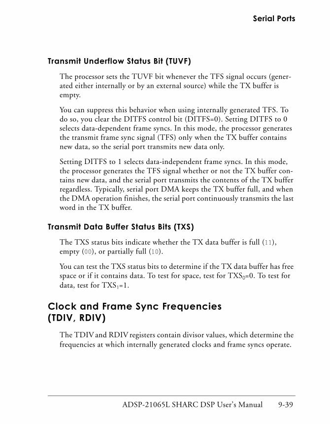
ADSP-21065L SHARC DSP User’s Manual 9-39
Serial Ports
Transmit Underflow Status Bit (TUVF)
The processor sets the TUVF bit whenever the TFS signal occurs (gener-ated either internally or by an external source) while the TX buffer is empty.
You can suppress this behavior when using internally generated TFS. To do so, you clear the DITFS control bit (DITFS=0). Setting DITFS to 0 selects data-dependent frame syncs. In this mode, the processor generates the transmit frame sync signal (TFS) only when the TX buffer contains new data, so the serial port transmits new data only.
Setting DITFS to 1 selects data-independent frame syncs. In this mode, the processor generates the TFS signal whether or not the TX buffer con-tains new data, and the serial port transmits the contents of the TX buffer regardless. Typically, serial port DMA keeps the TX buffer full, and when the DMA operation finishes, the serial port continuously transmits the last word in the TX buffer.
Transmit Data Buffer Status Bits (TXS)
The TXS status bits indicate whether the TX data buffer is full (11), empty (00), or partially full (10).
You can test the TXS status bits to determine if the TX data buffer has free space or if it contains data. To test for space, test for TXS0=0. To test for data, test for TXS1=1.
Clock and Frame Sync Frequencies(TDIV, RDIV)
The TDIV and RDIV registers contain divisor values, which determine the frequencies at which internally generated clocks and frame syncs operate.
SPORT Control Registers and Data Buffers
9-40 ADSP-21065L SHARC DSP User’s Manual
Figure 9-8 shows and Table 9-8 lists and defines the contents of theTDIV0 and TDIV1 registers.
Figure 9-8. TDIVx transmit divisor registers
Table 9-8. Transmit divisor register bit fields
Bits Name Definition
15-0 TCLKDIV Transmit clock divisor
31-16 TFSDIV Transmit frame sync divisor
31 30 29 28 27 26 25 24 23 22 21 20 19 18 17 16
15 14 13 12 11 10 9 8 7 6 5 4 3 2 1 0
TFSDIV
TCLKDIV
Transmit Frame Sync Divisor
Transmit Clock Divisor

ADSP-21065L SHARC DSP User’s Manual 9-41
Serial Ports
Figure 9-9 shows and Table 9-9 lists and defines the contents of the RDIV0 and RDIV1 registers.
Figure 9-9. RDIVx receive divisor registers
The TCLKDIV and RCLKDIV bit fields specify the number of times to divide the processor’s system clock (CLKIN) to generate the transmit and receive clocks. The divisor is a 16-bit value, which provides a wide range of serial clock rates.
Table 9-9. Receive divisor register bit fields
Bits Name Definition
15-0 RCLKDIV Receive clock divisor
31-16 RFSDIV Receive frame sync divisor
31 30 29 28 27 26 25 24 23 22 21 20 19 18 17 16
15 14 13 12 11 10 9 8 7 6 5 4 3 2 1 0
RFSDIV
RCLKDIV
Receive Frame Sync Divisor
Receive Clock Divisor

SPORT Control Registers and Data Buffers
9-42 ADSP-21065L SHARC DSP User’s Manual
Use this equation to calculate the serial clock frequency:
fCLKIN is the 1x frequency for the processor, and xCLKDIV is at least equal to 1.
Use this equation to calculate the value of xCLKDIV, given the CLKIN frequency and target serial clock frequency:
When frame sync is internally generated, TFSDIV and RFSDIV specify the number of transmit or receive clock cycles the processor counts before it generates a TFS or RFS pulse. You can use a frame sync this way to ini-tiate periodic transfers. The processor counts serial clock cycles whatever the clock source, internal or external.
Use this equation to calculate the number of serial clock cycles between frame synch pulses:
No. cycles between frame sync assertions = xFSDIV + 1
Use this equation to determine the value of xFSDIV, given the serial clock frequency and target frame sync frequency:
serial clock frequency 2xfCLKINxCLKDIV 1+( )
------------------------------------------=
xCLKDIV 2 f× CLKINserial clock frequency----------------------------------------------------- 1–=
xFSDIV serial clock frequencyframe sync frequency----------------------------------------------------- 1 –=
ADSP-21065L SHARC DSP User’s Manual 9-43
Serial Ports
The frame sync is continuously active if xFSDIV=0. However, to avoid causing an external device to abort the current operation or causing other unpredictable results, use a value for xFSDIV such that
FSDIV ≥ SLEN = serial word length −1
(Use the value of the SLEN field in the transmit or receive control register.)
If not using the serial port, you can use the xFSDIV divisor as a counter for dividing an external clock or for generating a periodic pulse or periodic interrupt. For this function, the serial port must be enabled.
Restrictions on Using Maximum Clock Rate
A delay occurs between the arrival of the transmit clock signal at the TCLKx pin and the output of serial data. This delay may limit the operat-ing speed of the receiver. For exact timing specifications, see the data sheet.
For reliable operation, we recommend that you use full-speed, serial clocks only when receiving with an externally generated clock and externally gen-erated frame sync (ICLK=0, IRFS=0).
Externally-generated, late transmit frame syncs (LAFS) experience a simi-lar delay between their arrival and data output, which can also limit the maximum speed of serial clocks. For exact timing specifications, see the data sheet.
Although the serial ports handle words with lengths of three to thirty-two bits, transmitting or receiving words smaller than four bits at the proces-sor’s full serial clock rate may cause loss of data when DMA chaining is enabled. Chaining takes over the processor’s internal I/O bus for several cycles while the DMA controller loads new TCB parameters. During this period, receive data in the RX buffer may be overwritten.

Data Word Formats
9-44 ADSP-21065L SHARC DSP User’s Manual
Data Word FormatsThe DTYPE, PACK, SENDN, and SLEN bits of the STCTLx and SRCTLx control registers format data words transmitted through the serial ports.
Data Type (DTYPE)The DTYPE field of the STCTLx and SRCTLx control registers, shown in Table 9-10, specifies the justification format and the companding format of the data when the serial port is configured for standard or multichannel operation.
For standard operation, the DTYPE field specifies one of four data for-mats. Data justification and companding formats are separate and exclusive options.
The RX and TX shifter registers apply these formats to serial data words when they are loaded into the RX and TX buffers. (Since only the signifi-cant bits of the serial data word are transmitted, the TX shift register does not actually zero-fill or sign-extend TX data words.)
For multichannel operation, the DTYPE field specifies one of four data types, as shown in Table 9-11. Because the justification and companding
Table 9-10. Data formats for nonmultichannel operation
DTYPE Data Formatting
00 Right justify; fill unused MSBs with zeros (0)
01 Right justify; extend sign into unused MSBs
10 Compand using µ -law
11 Compand using A-law

ADSP-21065L SHARC DSP User’s Manual 9-45
Serial Ports
format options function independently, the low bit specifies the justifica-tion format, and the high bit specifies the companding format.
The multichannel compand select registers, MTCCSx and MRCCSx, enable companding on specific transmit and receive channel slots. (For details, see “Channel Selection Registers (MTCSx, MRCSx, MTCCSx, MRCCSx)” on page 9-72.) Linear transfers occur on a channel slot that is active and has companding disabled. Companded transfers occur on a channel slot that is active and has companding enabled.
In STCTLx, bit 0 of DTYPE selects transmit sign extension for all trans-mit channels. In SRCTLx, bit 0 of DTYPE selects receive sign extension for all receive channels. With bit 0 set, sign extension occurs on selected channels that have companding disabled. If this bit is cleared, the data word contains 0s in its MSBs.
Companding
Companding (compressing and expanding) is the process of logarithmi-cally encoding and decoding data to minimize the number of bits that must be transmitted.
The processor’s serial ports support the two most widely used companding algorithms—A-law and µ-law—according to ITU G.711 specification. In standard and multichannel modes, you can select a companding algorithm
Table 9-11. Data formats for multichannel operation
DTYPE Data Formatting
x0 Right justify; fill unused MSBs with zeros (0)
x1 Right justify; extend sign into unused MSBs
0x Compand using µ -law
1x Compand using A-law

Data Word Formats
9-46 ADSP-21065L SHARC DSP User’s Manual
independently for each SPORT. (In standard mode, only the primary channels support companding.)The DTYPE field in the STCTLx and SRCTLx control registers selects the companding algorithm.
With companding enabled, the data in the Rx0_A or Rx1_A buffer is the right-justified, sign-extended expanded value of the eight LSBs received. Likewise, a write to Tx0_A and Tx1_A compresses the 32-bit value into eight LSBs (sign-extended to the width of the transmit word) before trans-mission. If the 32-bit value is greater than the13-bit A-law or 14-bit µ-law maximum, the TX buffer automatically compresses it to the maximum value.
Because the values in the TX and RX buffers are companded in place, you can use the companding hardware without transmitting (or receiving) data, for example, during testing or debugging. This operation requires a single cycle of overhead. For companding to execute properly, program the SPORT registers prior to loading data values into the SPORT buffers.
To compand data in place:
1. Enable companding.
Set the DTYPE field of the STCTLx transmit control register appropriately.
2. Write a 32-bit data word to TX.
(Companding is calculated in this cycle.)
3. Wait one cycle.
You can either insert a NOP instruction or not. Either way, the processor’s core is held off for one cycle. (This delay enables the serial port companding hardware to reload TX with the com-panded value.)
4. Read the 8-bit companded value from TX.
ADSP-21065L SHARC DSP User’s Manual 9-47
Serial Ports
To expand data in place, use the same procedure, but replace TX with RX. When performing this procedure, make sure to set the serial word length (SLEN) in the SRCTLx control register appropriately.
With companding enabled, interfacing the processor’s serial ports to a code requires little additional programming effort. With companding dis-abled, two formats for received data words of fewer than 32 bits are available (for details, see “Data Type (DTYPE)” on page 9-44).
Data Packing and Unpacking (PACK) You can pack received data words of sixteen bits or less into 32-bit internal data words, and unpack 32-bit internal data words into 16-bit data words for transmission.
The PACK bit in the SRCTLx and STCTLx control registers enable word packing and unpacking.
In SRCTLx:
PACK=1 Pack two words received successively into a single 32-bit word.
In STCTLx:
PACK=1 Unpack each 32-bit word into two 16-bit words and trans-mit.
Packing right-justifies the first 16-bit (or smaller) data word in bits 15-0 of the packed word and right-justifies the second 16-bit (or smaller) word in bits 31-16. This procedure reverses during transmit (unpacking) operations.
You can compand and pack/unpack data concurrently.
Data Word Formats
9-48 ADSP-21065L SHARC DSP User’s Manual
With packing enabled, 32-bit packed words, not each 16-bit data word, generates the transmit and receive interrupts.
Endian Format (SENDN)Endian format determines whether the processor transmits the serial word MSB-first or LSB-first.
The SENDN bit in the STCTLx and SRCTLx control registers select endian format.
SENDN_z=0 Transmit or receive serial words MSB-first.
SENDN_z=1 Transmit or receive serial words LSB-first.
Word Length (SLEN)The serial ports handle word lengths that range from three to thirty-two bits.
The five-bit SLEN field in the STCTLx and SRCTLx control registers configures the word length. The processor uses this value to determine how many bits to shift into or out of the shift register.
Using short word space addresses, you can read and write 16-bit data words that have been packed into 32-bit words and stored in normal word space in internal memory.

ADSP-21065L SHARC DSP User’s Manual 9-49
Serial Ports
The value of SLEN is equal to the word length minus one:
SLEN = Serial Word Length -1
The RX and TX buffers right-justify words smaller than thirty-two bits, so they occupy the least significant bit positions.
Transmitting or receiving words smaller than four bits at the processor’s full clock rate can cause loss of data when DMA chaining is enabled. Because chaining takes over the processor’s internal I/O bus for several cycles while the DMA controller loads new TCB chain parameters, received data in the RX buffer may be overwritten during this period.
SLEN ≠ 0 or 1
Clock Signal Options
9-50 ADSP-21065L SHARC DSP User’s Manual
Clock Signal OptionsEach serial port has a transmit clock signal TCLKx and a receive clock sig-nal RCLKx.
The ICLK and CKRE bits of the STCTLx and SRCTLx control registers configure the clock signals for standard and multichannel operation modes only.
The ICLK bits select the source of the transmit and receive clock signals. The CKRE bits select which clock edge (rising or falling) to use for syn-chronizing transmit and receive frames and for sampling data.
You configure the serial clock frequency in the TDIVx and RDIVx registers.
To use a single clock for both input and output, tie the receive clock pin to the transmit clock pin.
Internal vs. External ClocksYou can configure an internal or external clock source for the transmit and receive operations independently. The ICLK bit in the STCTLx and SRCTLx control registers selects the clock source.
When ICLK=1, the processor generates the clock signal, and the TCLKx or RCLKx pins are output pins.
The value of the serial clock divisor TCLKDIV or RCLKDIV in the TDIVx or RDIVx register, sets the clock frequency.
ADSP-21065L SHARC DSP User’s Manual 9-51
Serial Ports
When ICLK=0, the processor accepts the clock signal as an input on the TCLKx or RCLKx pins.
The processor does not require synchronization between an externally gen-erated serial clock and its system clock.
In this mode, the processor ignores the serial clock divisors in the TDIVx and RDIVx registers.

Frame Sync Options
9-52 ADSP-21065L SHARC DSP User’s Manual
Frame Sync OptionsFraming signals indicate the beginning of each serial word transfer. For frame sync operation, the processor supports a variety of framing options. Framing options on transmit and receive serial port channels are indepen-dent and configured separately in the STCTRLx and SRCTLx control registers.
The processor supports these frame sync options:
• Frame sync requirement (TFSR/RFSR)
• Frame sync source (ITFS/IRFS)
• Frame sync active state (LTFS/LRFS)
• Frame sync clock edge (CKRE)
• Frame sync insert (LAFS)
• Frame sync data dependency (DITFS)
Frame Sync Requirement (TFSR/RFSR)Using frame sync signals is optional in serial port communications. In standard mode only, the TFSR (transmit frame sync required) and RFSR (receive frame sync required) control bits determine whether frame sync signals are required.
When TFSR=1 or RFSR=1, every data word requires a frame sync signal. To enable continuous transmissions from the ADSP-21065L, the processor must load each new data word into the TX buffer before shifting out and transmitting the last bit of the previous word. (See “Frame Sync Data Dependency (DITFS)” on page 9-57.)
ADSP-21065L SHARC DSP User’s Manual 9-53
Serial Ports
When TFSR=0 or RFSR=0, data words do not require the corresponding frame sync signal, but initiating communications requires a single frame sync. After the processor transfers the first bit, it ignores the frame sync signal and continuously transmits data words unframed.
Figure 9-10 on page 9-54 shows framed serial transfers, which have the following characteristics:
• TFSR and RFSR bits in STCTLx, SRCTLx control registers deter-mine framed or unframed mode.
• Framed mode requires a framing signal for every word. Unframed mode ignores the framing signal after the first word.
• Unframed mode is appropriate for continuous reception.
• Active-low or active-high frame syncs selected with LTFS and LRFS bits of STCTLx, SRCTLx control registers.
When DMA is enabled with frame syncs not required, chaining may hold off DMA requests or the DMA controller may not ser-vice requests frequently enough to guarantee continuous, unframed data flow.
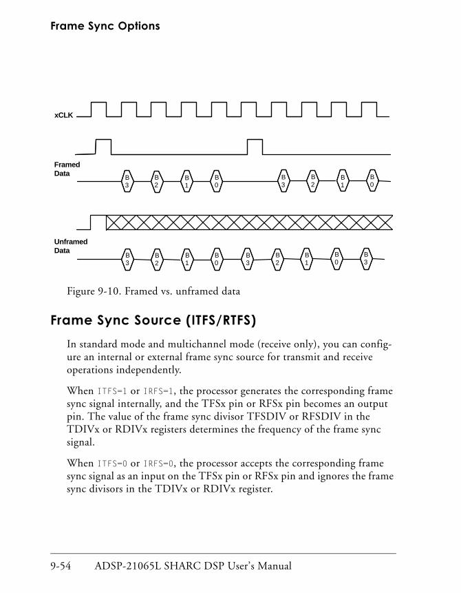
Frame Sync Options
9-54 ADSP-21065L SHARC DSP User’s Manual
Figure 9-10. Framed vs. unframed data
Frame Sync Source (ITFS/RTFS)In standard mode and multichannel mode (receive only), you can config-ure an internal or external frame sync source for transmit and receive operations independently.
When ITFS=1 or IRFS=1, the processor generates the corresponding frame sync signal internally, and the TFSx pin or RFSx pin becomes an output pin. The value of the frame sync divisor TFSDIV or RFSDIV in the TDIVx or RDIVx registers determines the frequency of the frame sync signal.
When ITFS=0 or IRFS=0, the processor accepts the corresponding frame sync signal as an input on the TFSx pin or RFSx pin and ignores the frame sync divisors in the TDIVx or RDIVx register.
B1
B1
B1
B2
B2
B2
B2
B1
B3
B3
B3
B3
B3
B0
B0
B0
B0
xCLK
FramedData
UnframedData

ADSP-21065L SHARC DSP User’s Manual 9-55
Serial Ports
All of the various frame sync options are available whether the signal is generated internally or externally.
Frame Sync Active State (LTFS/RTFS)In standard mode and multichannel mode, you can configure the logic level of frame sync signals for active high operation or for active low (inverted) operation.
When LTFS=0 or LRFS=0, the corresponding frame sync signal is active high. This value is the default configuration, and a processor reset initial-izes the LTFS and LRFS bits to 0.
When LTFS=1 or LRFS=1, the corresponding frame sync signal is active low.
Frame Sync Clock Edge (CKRE)In standard mode and multichannel mode, you can configure on which edge of serial port clock signals the processor samples data and frame syncs—either on the rising edge or on the falling edge.
For transmit data and frame syncs, setting CKRE=1 selects the rising edge of TCLKx. CKRE=0 selects the falling edge of TCLKx. Data and frame sync signals change state on whatever clock edge is not selected.
For receive data and frame syncs, setting CKRE=1 causes the processor to clock data in on the rising edge of RCLKx. CKRE=0 causes the processor to clock data in on the falling edge of RCLKx.
If you connect the transmit and receive functions of two serial ports together, make sure you configure the connections with the same value for CKRE, so the processor drives internally generated signals on one edge and samples received signals on the opposite edge.

Frame Sync Options
9-56 ADSP-21065L SHARC DSP User’s Manual
Frame Sync Insert (LAFS)In standard mode, you can configure when the processor generates frame sync signals (for multichannel mode, MFD=1, see page 9-67). Frame sync signals can occur during the first bit of each data word (late) or during the serial clock cycle immediately preceding the first bit (early).
Setting LAFS=0 selects early frame sync mode (normal operation). In this mode, the first bit of the transmit data word is available (and the first bit of the receive data word is latched) in the serial clock cycle after the frame sync is asserted, and the frame sync is not checked again until the entire word has been transmitted (or received). (In multichannel operation, this occurs when frame delay is 1.)
In early frame sync mode, if data transmission is continuous (the first bit of the next word immediately follows the last bit of each word), the frame sync signal occurs during the last bit of each word. In early frame sync mode, the processor asserts internally generated frame syncs for one clock cycle.
Setting LAFS=1 selects late frame sync mode. In this mode, the first bit of the transmit data word is available (and the first bit of the receive data word is latched) in the same serial clock cycle that the frame sync is asserted. (In multichannel operation, this occurs when frame delay is 0.)
Serial clock edges latch receive data bits, but the frame sync signal is checked during the first bit of each word only. In late frame sync mode, the processor continues to assert internally generated frame syncs for the entire length of the data word. Externally generated frame syncs are checked during the first bit only.
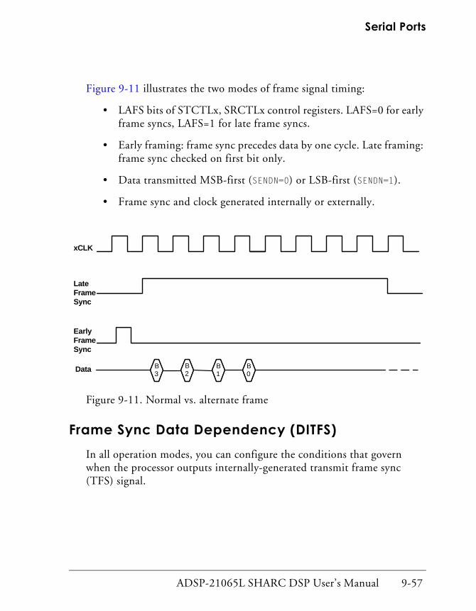
ADSP-21065L SHARC DSP User’s Manual 9-57
Serial Ports
Figure 9-11 illustrates the two modes of frame signal timing:
• LAFS bits of STCTLx, SRCTLx control registers. LAFS=0 for early frame syncs, LAFS=1 for late frame syncs.
• Early framing: frame sync precedes data by one cycle. Late framing: frame sync checked on first bit only.
• Data transmitted MSB-first (SENDN=0) or LSB-first (SENDN=1).
• Frame sync and clock generated internally or externally.
Figure 9-11. Normal vs. alternate frame
Frame Sync Data Dependency (DITFS)In all operation modes, you can configure the conditions that govern when the processor outputs internally-generated transmit frame sync (TFS) signal.
B3
B1
B2
B0
xCLK
LateFrameSync
Data
EarlyFrameSync
Frame Sync Options
9-58 ADSP-21065L SHARC DSP User’s Manual
Normally, the processor outputs a TFS only when the TX buffer has data ready to transmit (data-dependent transmit frame sync). DITFS (data-independent transmit frame sync) mode enables the processor to continu-ously generate the TFS signal, with or without new data.
When DITFS=0, the processor outputs TFS only when the TX buffer con-tains a new data word. Once loaded into the TX buffer, a new data word is transmitted two cycles after the processor generates the next TFS. Data-dependent mode provides the method to transmit data at specific times only.
When DITFS=1, the processor outputs TFS at its programmed interval, regardless of whether new data is available in the TX buffer. In data-inde-pendent mode, with each assertion of TFS, the processor transmits whatever data is present in the TX buffer. When old data is retransmitted, the processor sets the transmit underflow status bit (TUVF) in the STCTLx control register. The processor also sets the TUVF status bit if the TX buffer does not have new data when an externally generated TFS occurs. In data-independent mode, the first internally generated TFS is delayed until data has been loaded into the TX buffer.
With DITFS=1, initiating a transfer requires a single write to the TX data register.

ADSP-21065L SHARC DSP User’s Manual 9-59
Serial Ports
Standard ModeIn standard mode, you can enable either one or both of the SPORTs’ transmit channels. The frame sync source determines their transmit configuration.
When using both transmitters simultaneously, both TX buffers must con-tain data. For continuous transmission, both TX buffers must contain new data.
The receiving SPORT receives on both Rx_A and Rx_B. But only a SPORT with DMA enabled generates DMA requests or DMA interrupts upon receiving data.
Each SPORT transmit and receive channel has its own channel enable, DMA enable, and chaining enable bits in its STCTLx and SRCTLx con-trol register.
The SPORTs support companding on the primary channels, Tx_A and Rx_A, only.
Enabling Standard Mode (OPMODE, MCE)You enable standard mode with the OPMODE and MCE bits (STCTLx and SRCTLx). To do so, set both bits to 0.
Frame Sync Configuration (FS_BOTH)In standard mode, FS_BOTH (STCTLx) specifies when the processor generates the transmit frame sync signal.
FS_BOTH=0 Generate frame sync when data is available in either trans-mit channel.
FS_BOTH=1 Generate frame sync only when data is available in both transmit channels.

Standard Mode
9-60 ADSP-21065L SHARC DSP User’s Manual
When both transmitters are transmitting simultaneously (FS_BOTH=1), the processor generates frame syncs only when both transmitters contain data. For continuous transmission when using both transmitters simulta-neously, both transmitters must contain new data.
To implement this mode, you must also configure the processor for data-dependent TFS and as TFS source:
DITFS=0
ITFS=1
Setting the Serial Clock Frequency (CLKDIV)You can set the serial clock frequency for the processors internal clocks. For details see, “Clock and Frame Sync Frequencies (TDIV, RDIV)” on page 9-39.
ADSP-21065L SHARC DSP User’s Manual 9-61
Serial Ports
I2S ModeI2S mode supports the Inter-IC sound bus protocol developed for exchanging audio data between digital audio processors over a serial link.
The I2S bus transmits audio data and control signals over separate lines. The data line carries two multiplexed data channels, the left channel and the right channel.
In I2S mode:
• Both SPORT transmit channels (Tx_A and Tx_B) always transmit
simultaneously, each transmitting left and right I2S channels.
• Both SPORT receive channels (Rx_A and Rx_B) always receive
simultaneously, each receiving left and right I2S channels.
• Data always transmits in MSB format.
• You can select either DMA-driven or interrupt-drive data transfers.
• TFS and RFS are the transmit and receive word select signals.
• Multichannel operation and companding are not supported.
Each SPORT transmit and receive channel has its own channel enable, DMA enable, and chaining enable bits in its STCTLx and SRCTLx con-trol register.
Setting the Internal Serial Clock RateYou can program the serial clock rate (xCLKDIV value) for internal clocks in the CLKDIV registers. For details, see “Clock and Frame Sync Fre-quencies (TDIV, RDIV)” on page 9-39.

I2S Mode
9-62 ADSP-21065L SHARC DSP User’s Manual
In I2S mode, you must load both the TDIV register and the RDIV register with the same value as SLEN. For example, for 8-bit data words (SLEN=7), you must set TFSDIV = 7 and RFSDIV = 7.
I2S Control BitsSeveral bits in the STCTLx and SRCTLx control registers enable and con-
figure I2S operation:
• Operation mode (OPMODE)
• Multichannel enable (MCE)
• Word length (SLEN)
• I2S channel transfer order (L_FIRST)
• Frame sync (word select) generation (FS_BOTH)
• Master mode enable (MSTR)
• DMA enable (SDEN)
• DMA chaining enable (SCHEN)
Enabling I2S mode (OPMODE, MCE)
You enable I2S mode with the OPMODE and MCE bits (STCTLx and SRCTLx). With SPENx=1, set
OPMODE=1 Enable I2S mode
MCE=0 Disable multichannel mode
ADSP-21065L SHARC DSP User’s Manual 9-63
Serial Ports
Setting the Word Length (SLEN)
The SPORTs handle data words containing from 3 to 32 bits. You can set the number of bits transmit and receive data words contain. For details, see “Word Length (SLEN)” on page 9-48.
The transmitter always sends the MSB of the next word one clock cycle after the word select (TFS) signal changes.
In I2S mode, you must load the FSDIV register with the same value as SLEN. For example, for 8-bit data words (SLEN=7), you must set FSDIV= 7. For details, see “Clock and Frame Sync Frequencies (TDIV, RDIV)” on page 9-39.
Selecting the I2S Transmit and Receive Channel Order (L_FIRST)
You can configure which I2S channel each SPORT channel transmits or receives first. By default, the SPORT channels transmit and receive on the
right I2S channel first. The left and right I2S channels are time-duplexed data channels.
To select the channel order, set the L_FIRST bit:
L_FIRST=0 Transmit or receive on right channel first.
L_FIRST=1 Transmit or receive on left channel first.
Selecting the Frame Sync options (FS_BOTH)
The processor uses TFS and RFS as transmit and receive word select sig-nals. You can configure when the processor generates the transmit word select signal based on the data in the transmit channels.

I2S Mode
9-64 ADSP-21065L SHARC DSP User’s Manual
FS_BOTH=0 Generate word select signal if either transmit channel con-tains data.
FS_BOTH=1 Generate word select signal only if both transmit channels contain data.
The word select signal changes one clock cycle before the MSB of the data word transmits, enabling the slave transmitter to derive synchronous tim-ing of the serial data and enabling the receiver to store the previous data word and clear its input for the next one.
When using both transmitters (FS_BOTH=1) and MSTR=1 and DITFS=0, the processor generates a frame sync signal only when both transmit buffers contain data because both transmitters share the same CLKDIV and TFS. So, for continuous transmission, both transmit buffers must contain new data. To enable continuous transmission when only one transmit buffer contains new data, set FS_BOTH=0.
When using both transmitters and MSTR=1 and DITFS=1, the processor gen-erates a frame sync signal at the frequency set by FSDIV=x whether or not the transmit buffers contain new data. In this case, the processor ignores the FS_BOTH bit. The DMA controller or the application is responsible for filling the transmit buffers with data.
Enabling SPORT Master Mode (MSTR)
You can configure the SPORTs transmit and receive channels for master or slave mode. In master mode, the processor generates the word select and serial clock signals for the transmitter or receiver internally. In slave mode, an external source generates the word select and serial clock signals for the transmitter or receiver.
MSTR=0 Use external word select and clock source; transmitter or receiver is slave.
MSTR=1 Use processor’s internal clock for word select and clock source; transmitter or receiver is master.

ADSP-21065L SHARC DSP User’s Manual 9-65
Serial Ports
Enabling SPORT DMA (SDEN)
You can enable or disable DMA independently on any of the SPORT’s transmit and receive channels.
SDEN_z=0 Disables DMA and set channel in interrupt-driven data transfer mode.
SDEN_z=1 Enable DMA and set channel in DMA-driven data transfer mode.
Interrupt-Driven Data Transfer Mode. In this mode, both transmit-ters share a common interrupt vector and both receivers share a common interrupt vector.
The SPORT generates an interrupt whenever the transmit buffer has a vacancy or whenever the receive buffer has data. To determine the source of an interrupt, applications must check the TXSx or RXSx data buffer status bits, respectively.
DMA-Driven Data Transfer Mode. Each transmitter and receiver has its own set of DMA registers. (For details, see Chapter 6, DMA.) The
same DMA channel drives both the left and right I2S channels for the transmitter or for the receiver. The software application must demultiplex the left and right channel data received by the RX buffer.
Both transmitters share a common interrupt vector and both receivers share a common interrupt vector. The DMA controller generates an inter-rupt at the end of DMA transfer only.

I2S Mode
9-66 ADSP-21065L SHARC DSP User’s Manual
Figure 9-12 shows the relationship between FS (word select), serial clock,
and I2S data. Timing for word select is the same as for frame sync. (Note that this example uses early frame sync.)
Figure 9-12. Word select timing in I2S mode
A1
A2
A3
B1
B2
B3
xCLK
FS/WS
I2SData
Left Channel Right Channel

ADSP-21065L SHARC DSP User’s Manual 9-67
Serial Ports
Multichannel ModeThe processor’s serial ports support multichannel operation, which enables a SPORT to communicate in a time-division-multiplexed (TDM) serial system.
In multichannel communications, each data word in the serial bit stream occupies one channel slot. Data word 0 occupies channel slot 0, data word 1 occupies channel slot 1, …, and data word n occupies channel slot n. In this way, each data word in the stream belongs to the next consecutive channel slot so that, for example, a 24-word block of data contains one word for each of 24 channel slots.
A SPORT can automatically select words for particular channel slots while ignoring others. The processor supports up to thirty-two channel slots for transmitting or receiving—each SPORT can receive and transmit data selectively from any of the thirty-two channel slots.
On each channel slot, a SPORT can:
• Transmit data
• Receive data
• Transmit and receive data
• Do nothing
Multichannel mode also supports data companding and DMA transfers.
In this mode only, if the SPORT is enabled, the processor puts the DT pin in a high-impedance state when an inactive channel slot occurs.
In multichannel mode, the TCLKx pin is always an input and must connect to its corresponding RCLKx pin.

Multichannel Mode
9-68 ADSP-21065L SHARC DSP User’s Manual
Figure 9-13 shows example timing for a multichannel transfer, which has the following characteristics:
• Uses TDM method, where serial data is sent or received on different channel slots sharing the same serial bus.
• The number of channel slots is selected with the NCH bits of SRCTLx: NCH=(# of channels) – 1.
• Can independently select transmit and receive channels.
• RFS signals start of frame.
• TFS is used as “Transmit Data Valid” for external logic; active only during transmit channels.
• Example: Receive on channels 0 and 2 and transmit on channels 1 and 2.
Figure 9-13. Multichannel operation
B2
SCLK
DR
RFS
B3 B2 B1 B0 B3 B2
IGNOREDB0 B3
TFS
DT
B1B2B3
WORD 0 WORD 1 WORD 2

ADSP-21065L SHARC DSP User’s Manual 9-69
Serial Ports
Frame Syncs in Multichannel ModeAll receiving and transmitting devices in a multichannel system must have the same timing reference. The RFS signal provides this reference, indicat-ing the start of a block (or frame) of multichannel data words.
With multichannel mode enabled, the SPORT’s transmitter and receiver both use RFS as a frame sync, whether RFS is internally or externally gen-erated. The RFS signal synchronizes the channel slots and restarts each multichannel sequence. RFS assertion occurs at the beginning of the chan-nel 0 data word.
TFS functions as a transmit data valid signal, which is active during trans-mission of an enabled word. Since the processor puts the serial port’s DTx pin in a high-impedance state when the time slot is inactive, the TFS sig-nal specifies whether or not the processor is driving the DTx pin. The processor drives TFS in multichannel mode, whether or not ITFS=0 (external TFS source).
Transmission begins after the TX transmit buffer is loaded and the proces-sor generates the TFS signal. With serial port DMA enabled, transmission can occur several cycles after the multichannel transmission is enabled. If your application requires a deterministic start time, have it preload the TX buffer.
In multichannel mode, TFS remains unconnected normally, and the serial ports’ RFS pins connect together.
Multichannel Control BitsSeveral bits in the STCTLx and SRCTLx control registers enable and con-figure multichannel operation:
• Operation mode (OPMODE)
• Multichannel enable (MCE)

Multichannel Mode
9-70 ADSP-21065L SHARC DSP User’s Manual
• Number of channel slots (NCH)
• Current channel slot indicator (CHNL)
• Multichannel frame delay (MFD)
• Channel slot transmit/receive select (MTCS/MRCS)
• Channel slot transmit/receive compand select (MTCCS/MRCCS)
Operation Mode (OPMODE)
The operation mode bit enables and disables I2S mode and redefines the SPORT control bits accordingly. The multichannel enable (MCE) bit
affects SPORT operation only when I2S mode is disabled.
Multichannel Enable (MCE)
Setting the MCE bit enables multichannel mode only when OPMODE=0.
MCE=1 Enable multichannel operation.
MCE=0 Disable all multichannel operations.
Multichannel operation activates three cycles after MCE is set. Internally generated frame sync signals activate four cycles after MCE is set.
Setting the MCE bit enables multichannel operation for the SPORTs pri-mary set of transmit and receive channels. Therefore, if the receiving SPORT is in multichannel mode, the transmitting SPORT is too.
ADSP-21065L SHARC DSP User’s Manual 9-71
Serial Ports
Number of Channel Slots
The five-bit NCH field (SRCTLx) sets the number of channel slots to use in multichannel operation. Set NCH to the actual number of channels minus one:
NCH = Number of Channels −1
The SPORTs support up to thirty-two channel slots.
Current Channel Selected
The five-bit CHNL field (STCTLx) indicates which channel slot is cur-rently selected during multichannel operation. This field is a read-only status indicator. CHNL(4:0) increments modulo NCH(4:0) as the SPORT services each channel slot.
Multichannel Frame Delay
The four-bit MFD field (STCTLx) specifies a delay, in number of serial clock cycles, between the frame sync pulse and the first data bit in multi-channel mode. Multichannel frame delay enables the processor to work with different types of T1 interface devices.
MFD=0 No delay; frame sync concurrent with the first data bit.
MFD=x Frame sync delayed x clock cycles.
The maximum is 15 clock cycles. Because blocks of data occur back to back, new frame sync may occur before data from the last frame has been received.
When the processor is RFS source in a multiprocessor system and the sys-tem’s serial clock is equal to CLKIN (processor clock), use an MFD ≥ 1. Otherwise, the system’s master processor will not recognize the first frame sync after multichannel operation has been enabled. (It will, however, rec-ognize all succeeding frame syncs.)

Multichannel Mode
9-72 ADSP-21065L SHARC DSP User’s Manual
Channel Selection Registers (MTCSx, MRCSx, MTCCSx, MRCCSx)
You can enable and disable specific channel slots individually to select which words are received and transmitted during multichannel communications.
The processor transmits and receives only data words from enabled chan-nel slots and ignores data words on disabled channel slots. The SPORTs support a maximum of thirty-two channel slots for transmitting and for receiving.
The multichannel selection registers enable and disable (activate and deac-tivate) individual transmit and receive channel slots and enable and disable companding on them. Table 9-12 lists the registers for each serial port.
Each register has thirty-two bits that correspond to the thirty-two channel slots. Setting a bit activates the corresponding channel slot, so the SPORT
Table 9-12. Multichannel selection register definitions
Register Selects…
MTCSx Multichannel transmit select.
Specifies the active transmit channels.
MRCSx Multichannel receive select.
Specifies the active receive channels.
MTCCSx Multichannel transmit compand select.
Specifies which active channels are companded.
MRCCSx Multichannel receive compand select.
Specifies which active receive channels are com-panded.
ADSP-21065L SHARC DSP User’s Manual 9-73
Serial Ports
selects the data word it contains from the multiple-word data block. For example, setting bit 0 selects data word 0, setting bit 12 selects data word 12, and so on.
Setting a particular bit to 1 in the MTCSx register causes the SPORT to transmit the data word in that channel slot’s position in the data stream. Clearing the bit to 0 puts the SPORT’s DT (data transmit) pin into Hi-Z during the time of that channel slot.
Setting a particular bit to 1 in the MRCSx register causes the SPORT to receive the data word in that channel slot’s position in the data stream. The processor loads the received word into the RX buffer. Clearing the bit to 0 causes the SPORT to ignore the data.
You can also select companding on a per channel basis. The MTCCSx and MRCCSx registers specify companding for any active channel slots. Set-ting a bit to 1 in these registers causes the SPORT to compand the data word using either the A-law or µ-law companding algorithm. All channels configured for companding must use the same companding algorithm. (To select the companding algorithm, see “Data Type (DTYPE)” on page 9-44).
SPORT Receive Comparison Registers (KEYWDx and IMASKx)
In SPORT multichannel mode (MCE=1), the 32-bit receive comparison (KEYWDx) and receive comparison mask (IMASKx) registers aid multi-processor communications.
The KEYWDx register stores the pattern against which to match the incoming data. The corresponding IMASKx register specifies which bits in the received data to compare. Setting a bit in IMASKx to 1 masks the cor-responding bit in the KEYWDx register, removing it from comparison.
The receiving processor compares the received data with the data pattern in its KEYWDx register. Depending on the results, the processor accepts

Multichannel Mode
9-74 ADSP-21065L SHARC DSP User’s Manual
the received data or ignores it. On acceptance, depending on the SDENx setting in SRCTLx, the receiver either requests a DMA transfer to internal memory or generates an interrupt.
These bits (SRCTL) control the operation of the receive comparison in multichannel mode, as shown in Table 9-13.
With receive comparison enabled, companding is disabled on both trans-mitter and receiver.
The MTCCSx register, which selects multichannel companding when receive comparison is disabled, determines whether the DSP performs a KEYWD comparison for the enabled received channel slots.
MTCCSx=0 On channel slot x, disable receive comparison and always accept received data.
MTCCSx=1 On channel slot x, enable comparison and accept or reject received data based on comparison results and IMAT value (SRCTLx).
The receive comparison feature enables the SPORT to determine whether to generate either a DMA request or an interrupt when received data matches a specified condition on a specified channel. Otherwise, every time it received data the SPORT would have to interrupt the processor,
Table 9-13. SRCTL control bits for receive comparison
IMODE IMAT Selects…
0 x Receive comparison disabled.
1 0 Accept receive data if the KEYWD compares false.
1 1 Accept receive data if the KEYWD compares true.
ADSP-21065L SHARC DSP User’s Manual 9-75
Serial Ports
which would have to determine whether the data was meant for it. And SPORT data is often in transit to other than the processor. With the receive comparison feature, you can program a SPORT on a particular processor to interrupt only on messages meant for its processor.
For example, consider two ADSP-21065s (A and B) which use SPORT0 in multichannel mode for interprocessor communications. Processors A and B use channel slots 0 and 1, respectively, to transmit control information between them. To transmit data, processor A uses channel slots 2 through 16, and processor B uses channel slots 17 through 31.
Because channel slots 0 and 1 carry control information between the pro-cessors, receive comparison on incoming data is enabled only on these channel slots. Initially, receive may be disabled on channel slots 2 through 31. In this example, the programmed key word for processor B to compare against is START TRANSMIT TO B.
To check for this keyword, processor B:
1. Sets the KEYWDx register to START TRANSMIT TO B.
2. In IMASKx, sets bits 31:16 to 0 and sets bits 15:0 to 1
This step enables receive comparison on bits 31:16 only. Assume that the code for START TRANSMIT TO B uses bits 31:16 only and that bits 15:0 indicate the transmission source and data channel slots.
3. Sets the IMODE and IMAT (SRCTLx) bits to 1.
This step enables the SPORT to generate either an interrupt or DMA request only if the incoming data matches the KEYWDx.
4. Sets bits 0 and 1 of MTCCSx to 1 and clears the remaining bits 31:2.
This step enables comparison only on channel slots 0 and 1.

Multichannel Mode
9-76 ADSP-21065L SHARC DSP User’s Manual
Communication between the two processors follows this sequence:
1. Until it receives the START TRANSMIT TO B keyword, processor B ignores all transmissions that it receives.
2. To initiate transmission to B, processor A sends the START TRANS-MIT TO B keyword on channel slot 0.
3. When processor B’s receive comparison logic recognizes the START TRANSMIT TO B keyword, the SPORT interrupts its processor.
4. Processor B analyzes the remaining 16-bits and determines that the transmit source is processor A and that the data is on channel slots 2:16.
5. Because processor A is using channel slots 2 through 16 to transmit data, processor B enables receive channel slots 2 through 16 and sends a READY TO RECEIVE DATA message to processor A on channel slot 1.
6. After receiving this message, processor A sends the data on channel slots 2 through 16.
If the transfer protocol uses a fixed number of bytes in each mes-sage, to confirm that the data transferred accurately, processor B can return a checksum message to processor A after receiving A's message.

ADSP-21065L SHARC DSP User’s Manual 9-77
Serial Ports
Moving Data Between SPORTs and Memory
You can transfer transmit and receive data between the SPORTs and on-chip memory in one of two ways: with single-word, core transfers or with DMA block transfers. Both methods are interrupt-driven and use the same internally generated interrupts.
When serial port DMA is disabled (STCTLx or SRCTLx), the SPORT generates an interrupt every time it receives a data word or starts to trans-mit a data word.
SPORT DMA provides a mechanism for receiving or transmitting an entire block of serial data before the SPORT generates the interrupt. The processor’s on-chip DMA controller handles the DMA transfer, enabling the core to continue executing program until the entire block of data has been transmitted or received. Service routines that operate on blocks of data instead of single words significantly reduce overhead.
DMA Block TransfersThe processor’s on-chip DMA controller enables automatic DMA trans-fers between internal memory and the two serial ports.
Eight DMA channels support serial port operations—each SPORT has two channels for receiving data and two channels for transmitting data. Table 9-14 on page 9-78 lists each serial port DMA channels and its data buffer.

Moving Data Between SPORTs and Memory
9-78 ADSP-21065L SHARC DSP User’s Manual
Because of their relatively low service rate and their inability to hold off incoming data, the SPORT DMA channels have higher priority than external port DMA channels. Because they have higher priority, the DMA controller performs SPORT DMA transfers first when it receives multiple DMA requests in the same cycle.
Although DMA transfers always use 32-bit words, the serial ports can han-dle word sizes from 3 to 32 bits. If serial words are 16 bits or smaller, the SPORTs can pack them into 32-bit words for each DMA transfer. You configure packing with the PACK bit in the STCTLx and SRCTLx con-trol registers.
Table 9-14. DMA serial port channels
Channel Data Buffer
Description Priority
1 Rx0_A SPORT0 Receive, A data Highest
2 Rx0_B SPORT0 Receive, B data
3 Rx1_A SPORT1 Receive, A data
4 Rx1_B SPORT1 Receive, B data
5 Tx0_A SPORT0 Transmit, A data
6 Tx0_B SPORT0 Transmit, B data
7 Tx1_A SPORT1 Transmit, A data
8 Tx1_B SPORT1 Transmit, B data
9 EPB0 External port FIFO buffer 0
10 EPB1 External port FIFO buffer 1 Lowest

ADSP-21065L SHARC DSP User’s Manual 9-79
Serial Ports
With packing enabled (PACK=1), the SPORT generates the transmit and receive interrupts for the 32-bit packed words, not for each 16-bit serial word.
The following sections describe serial port DMA operations. For details on other DMA operations, see Chapter 6, DMA.
Setting Up DMA on SPORT Channels
Each SPORT DMA channel has an enable bit SDEN in its STCTLx and SRCTLx control registers.
When DMA is disabled for a particular channel, the SPORT generates an interrupt every time it receives a data word or starts transmitting a data word (see “Single-Word Transfers” on page 9-86).
Each channel also has a DMA chaining enable bit SCHEN in its STCTLx and SRCTLx control registers. For details, see “SPORT DMA Chaining” on page 9-85.
To set up a serial port DMA channel, you write a set of memory buffer parameters to the SPORT DMA parameter registers shown in Table 9-15 on page 9-80. Note that xy in the register names in the Register column indicates four registers, and each corresponds to a different DMA channel. For example, IIRxy represents IIR0A – DMA channel 0, IIR0B – DMA channel 1, IIR1A – DMA channel 2, and IIR1B – DMA channel 3. For a complete list of these registers, see the Symbol Definitions File (def21065L.h) in the ADSP-21065L SHARC DSP Technical Reference.
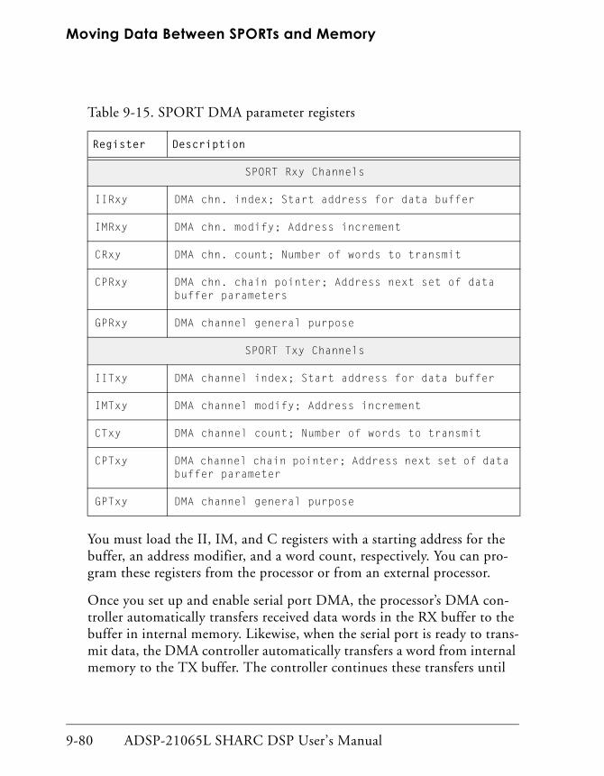
Moving Data Between SPORTs and Memory
9-80 ADSP-21065L SHARC DSP User’s Manual
You must load the II, IM, and C registers with a starting address for the buffer, an address modifier, and a word count, respectively. You can pro-gram these registers from the processor or from an external processor.
Once you set up and enable serial port DMA, the processor’s DMA con-troller automatically transfers received data words in the RX buffer to the buffer in internal memory. Likewise, when the serial port is ready to trans-mit data, the DMA controller automatically transfers a word from internal memory to the TX buffer. The controller continues these transfers until
Table 9-15. SPORT DMA parameter registers
Register Description
SPORT Rxy Channels
IIRxy DMA chn. index; Start address for data buffer
IMRxy DMA chn. modify; Address increment
CRxy DMA chn. count; Number of words to transmit
CPRxy DMA chn. chain pointer; Address next set of data buffer parameters
GPRxy DMA channel general purpose
SPORT Txy Channels
IITxy DMA channel index; Start address for data buffer
IMTxy DMA channel modify; Address increment
CTxy DMA channel count; Number of words to transmit
CPTxy DMA channel chain pointer; Address next set of data buffer parameter
GPTxy DMA channel general purpose

ADSP-21065L SHARC DSP User’s Manual 9-81
Serial Ports
the entire data buffer is received or transmitted—when the count register reaches zero.
When the count register of an active DMA channel reaches zero (0), the SPORT generates the corresponding interrupt.
SPORT DMA Parameter Registers
A DMA channel consists of a set of parameter registers that implement a data buffer in internal memory and the hardware that the serial port uses to request DMA service.
The parameter registers for each SPORT DMA channel are shown in Table 9-15 on page 9-80. These registers are part of the processor’s mem-ory-mapped IOP register set, and their addresses are shown in Table 9-16 on page 9-82.
The DMA channels operate similarly to the processor’s data address gener-ators (DAGs). Each channel has an index register (II) and a modify register (IM) for setting up a data buffer in internal memory. You must initialize the index register with the starting address of the data buffer. After it transfers each serial I/O word to or from the SPORT, to generate the address for the next DMA transfer, the DMA controller adds the mod-ify value to the index register. The modify value in the IM register is a signed integer, which provides capability for both incrementing and decre-menting the buffer pointer.
Each DMA channel has a count register C, which you must initialize with a word count that specifies the number of words to transfer. The count register decrements after each DMA transfer on the channel. When the word count reaches zero, the SPORT generates the interrupt for the chan-nel and automatically disables the DMA channel. The DEN bit in the SxCTLx register is not cleared and should be cleared before a new DMA is started.
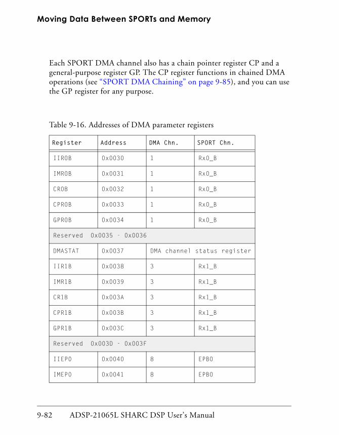
Moving Data Between SPORTs and Memory
9-82 ADSP-21065L SHARC DSP User’s Manual
Each SPORT DMA channel also has a chain pointer register CP and a general-purpose register GP. The CP register functions in chained DMA operations (see “SPORT DMA Chaining” on page 9-85), and you can use the GP register for any purpose.
Table 9-16. Addresses of DMA parameter registers
Register Address DMA Chn. SPORT Chn.
IIR0B 0x0030 1 Rx0_B
IMR0B 0x0031 1 Rx0_B
CR0B 0x0032 1 Rx0_B
CPR0B 0x0033 1 Rx0_B
GPR0B 0x0034 1 Rx0_B
Reserved 0x0035 - 0x0036
DMASTAT 0x0037 DMA channel status register
IIR1B 0x0038 3 Rx1_B
IMR1B 0x0039 3 Rx1_B
CR1B 0x003A 3 Rx1_B
CPR1B 0x003B 3 Rx1_B
GPR1B 0x003C 3 Rx1_B
Reserved 0x003D - 0x003F
IIEP0 0x0040 8 EPB0
IMEP0 0x0041 8 EPB0

ADSP-21065L SHARC DSP User’s Manual 9-83
Serial Ports
CEP0 0x0042 8 EPB0
CPEP0 0x0043 8 EPB0
GPEP0 0x0044 8 EPB0
EIEP0 0x0045 8 EPB0
EMEP0 0x0046 8 EPB0
ECEP0 0x0047 8 EPB0
IIEP1 0x0048 9 EPB1
IMEP1 0x0049 9 EPB1
CEP1 0x004A 9 EPB1
CPEP1 0x004B 9 EPB1
GPEP1 0x004C 9 EPB1
EIEP1 0x004D 9 EPB1
EMEP1 0x004E 9 EPB1
ECEP1 0x004F 9 EPB1
IIT0B 0x0050 5 Tx0_B
IMT0B 0x0051 5 Tx0_B
CT0B 0x0052 5 Tx0_B
CPT0B 0x0053 5 Tx0_B
GPT0B 0x0054 5 Tx0_B
Table 9-16. Addresses of DMA parameter registers (Cont’d)
Register Address DMA Chn. SPORT Chn.

Moving Data Between SPORTs and Memory
9-84 ADSP-21065L SHARC DSP User’s Manual
Reserved 0x0055 - 0x0057
IIT1B 0x0058 7 Tx1_B
IMT1B 0x0059 7 Tx1_B
CT1B 0x005A 7 Tx1_B
CPT1B 0x005B 7 Tx1_B
GPT1B 0x005C 7 Tx1_B
Reserved 0x005D - 0x005F
IIR0A 0x0060 0 Rx0_A
IMR0A 0x0061 0 Rx0_A
CR0A 0x0062 0 Rx0_A
CPR0A 0x0063 0 Rx0_A
GPR0A 0x0064 0 Rx0_A
Reserved 0x0065 - 0x0067
IIR1A 0x0068 2 Rx1_A
IMR1A 0x0069 2 Rx1_A
CR1A 0x006A 2 Rx1_A
CPR1A 0x006B 2 Rx1_A
GPR1A 0x006C 2 Rx1_A
Reserved 0x006D - 0x006F
Table 9-16. Addresses of DMA parameter registers (Cont’d)
Register Address DMA Chn. SPORT Chn.

ADSP-21065L SHARC DSP User’s Manual 9-85
Serial Ports
SPORT DMA Chaining
In chained DMA operations, the processor’s DMA controller automati-cally sets up another DMA transfer when the contents of the current buffer have been transmitted (or received). The chain pointer register (CP) functions as a pointer to the next set of buffer parameters stored in memory. The DMA controller automatically downloads these buffer parameters to set up the next DMA sequence. For details, see Chapter 6, DMA.
DMA chaining occurs independently for the transmit and receive channels of each serial port. Each SPORT DMA channel has a chaining enable bit SCHEN (STCTLx and SRCTLx).
IIT0A 0x0070 4 Tx0_A
IMT0A 0x0071 4 Tx0_A
CT0A 0x0072 4 Tx0_A
CPT0A 0x0073 4 Tx0_A
GPT0A 0x0074 4 Tx0_A
Reserved 0x0075 - 0x0077
IIT1A 0x0078 6 Tx1_A
IMT1A 0x0079 6 Tx1_A
CT1A 0x007A 6 Tx1_A
CPT1A 0x007B 6 Tx1_A
GPT1A 0x007C 6 Tx1_A
Table 9-16. Addresses of DMA parameter registers (Cont’d)
Register Address DMA Chn. SPORT Chn.

Moving Data Between SPORTs and Memory
9-86 ADSP-21065L SHARC DSP User’s Manual
SCHEN_z=0 Disable DMA chaining
SCHEN_z=1 Enable DMA chaining
(You can also write all 0s to the address field of the chain pointer register (CP) to disable chaining.)
Single-Word TransfersThe SPORTs can also transfer individual data words, generating interrupts for each 32-bit word transfer.
When a serial port is enabled and DMA is disabled (STCTLx or SRCTLx), the SPORT generates DMA interrupts whenever:
• The RX buffer has received an entire word.
• The TX buffer is not full.
This behavior enables you to use single-word interrupts to implement interrupt-driven I/O on the serial ports.
Whenever the processor’s core program reads a word from a serial port’s RX buffer or writes a word to its TX buffer, make sure it checks the buffer’s full/empty status first to avoid hanging the core. (This can happen to an external device too, such as a host processor, when it is reading or writing a serial port buffer.) To check buffer status, read the RXS bits or the TXS bits in the SRCTLx or STCTLx control register.
Reading from an empty RX buffer or writing to a full TX buffer causes the processor (or external device) to hang, waiting for the status to change. To prevent this hang condition, in the SYSCON register, set the BHD (Buffer Hang Disable) bit to 1.
The processor updates the status bits in STCTLx and SRCTLx during core reads and writes, even when the serial port is disabled. For details, see page 9-7.

ADSP-21065L SHARC DSP User’s Manual 9-87
Serial Ports
Multiple interrupts can occur if both SPORTs transmit or receive data in the same cycle. You can mask out any interrupt in the IMASK register. If you re-enable the interrupt in IMASK later, clear the corresponding inter-rupt latch bit in IRPTL in case the interrupt occurred while it was masked.
With serial port data packing enabled (PACK=1), the SPORT generates the transmit and receive interrupts for the 32-bit packed words, not for each 16-bit serial word.
SPORT Loopback
9-88 ADSP-21065L SHARC DSP User’s Manual
SPORT LoopbackIn standard and I2S modes, the SPL bit (SPORT loopback mode) in the SRCTLx control register configures the serial port for internal loopback connection. SPORT loopback mode enables you to test the serial port’s internal operation.
SPL=0 Disable SPORT loopback mode.
SPL=1 Enable SPORT loopback mode.
With loopback enabled, the DRx, RCLKx, and RFSx signals of the SPORT’s receive section internally connect to the DTx, TCLKx, and TFSx signals of the transmit section. The DTx, TCLKx, and TFSx signals are active and available at their respective pins, while the processor ignores the DRx, RCLKx, and RFSx pins.
In loopback mode, you can use only the transmit clock and transmit frame sync options, and you must make sure that you set up the serial port cor-rectly in the STCTLx and SRCTLx control registers.
Loopback mode does not support multichannel operation.
SPORT Pin Driver ConsiderationsThe processor has very fast drivers on all output pins, including the serial ports. If connections on the data, clock, or frame sync lines are longer than six inches, we recommend that you use a series termination for strip lines on point-to-point connections. Because of the edge rates, this hard-ware may be necessary even for low-speed serial clocks.
ADSP-21065L SHARC DSP User’s Manual 9-89
Serial Ports
SPORT Programming ExamplesThe processor provides three ways to control serial port communications and memory-to-SPORT data transfers:
• Single-word transfers under core processor control with no inter-rupts.
• Single-word transfers under core processor control with interrupts.
• DMA transfers with interrupts.
The three examples presented next illustrate each of these methods. Each example uses SPORT0 to transmit eight 32-bit words from a data buffer in internal memory.
Each of the three control schemes also operates in multichannel mode and with any of the serial clock and frame sync options.
Single-Word Transfers Without Interrupts The processor’s core will stall (i.e. hang) when it attempts to write data to a full TX buffer or read data from an empty RX buffer. This provides a very simple method of controlling the SPORT—placing the instruction that writes data to TX or reads data from RX in a loop. Program execution will stall at this instruction, until the SPORT is ready to transmit new data or has received new data.
Listing 9-1 on page 9-90 shows the code for this example, which sets up a loop to transmit data out of SPORT0. Although this technique provides a very simple programming solution, it prevents the processor’s core from handling any other tasks while waiting for the serial port. The interrupt-driven technique described in the following section alleviates this.
SPORT Programming Examples
9-90 ADSP-21065L SHARC DSP User’s Manual
Listing 9-1. SPORT transmit example code
/* */SPORT Transmit Example: Uses the feature that the processor core will stall when attempting to write to a full TX register. This example sets up a loop to transmit the data in the memory buffer source./* */
#define N 8#include “def21065L.h” /* Use symbolic register name */
.segment/dm dm32_b1; /* Data segment name described in ldf file */
.var source[N]= 0x11111111, 0x22222222, 0x33333333, 0x44444444 0x55555555, 0x66666666, 0x77777777, 0x88888888;
.endseg;
.segment/pm rst_svc; /* Reset vector from ldf file */nop; /* First location is used for booting */jumpstart;
.endseg;
/* Main Routine */
.segment/pm pm48_1b0; /* Main code segment from ldf file. */
start:r0=0x00270007; /* TDIV0 register: TCLKDIV=7,TFSDIV=39 */dm(TDIV0)=r0; /* sclock=CLKIN/8, framerate=sclock/20 */
r0=0x000064f1; /* STCTL0 register */dm(STCTL0)=r0; /* SPEN=1, (SPORT enabled) */
/* SLEN=15, (16-bit word) *//* ICLK=1, (internal tx clock) *//* TFSR=1, (require TFS) *//* ITFS=1, (internal TFS) *//* DITFS=0, (data-depedent FS) */
b0=source; /* Pointer to source; i0=b0 automatically */10=@source;

ADSP-21065L SHARC DSP User’s Manual 9-91
Serial Ports
lcntr=N, do tx_loop until lce;r0=dm(i0,1); /* Get data from source buffer. */
tx_loop: dm(TX0_A)=r0; /* Write transmit register, core *//* will wait until SPORT output *//* buffer is not full */
idle;.endseg;/* */
Single-Word Transfers with InterruptsWhile the non-interrupt-driven solution of the previous example provides a very simple control scheme, it prevents the processor’s core from han-dling any additional tasks while it is stalled. In most real-time applications, the DSP must process data while new data is being received. It may also need to perform background tasks between data transfers.
In most systems, therefore, the DSP processor must be able to continue executing its program at all times. Using the serial port receive and trans-mit interrupts allows this to happen, by interrupting the core processor only when a new data word has been received or when a new data word can be transmitted. The interrupt service routine then performs the data transfer between internal memory and the serial port’s TX or RX buffer.
Listing 9-2 shows the code for this example. Note that the interrupt used is the SPORT0 Transmit DMA Channel interrupt (SPT0I)—when serial port DMA is disabled, this interrupt becomes a single-word transmit interrupt.
Listing 9-2. SPORT interrupt-driven transmit example
/* */2106x Interrupt Driven SPORT Transmit ExampleThis example uses interrupts to notify the core when new data isrequired. The buffer “source” is transmitted.
/* */#define N 8#include “def21065L.h” /*Use symbolic register names */.segment/dm dm32_b1; /* Data segment name described in ldf file */

SPORT Programming Examples
9-92 ADSP-21065L SHARC DSP User’s Manual
.var source[N]= 0x11111111, 0x22222222, 0x33333333, ox44444444 0x55555555, 0x66666666, 0x77777777, 0x88888888
.endseg;
.segment/pm rst_svc; /* Reset vector from ldf file. */nop; /* First location is used for booting */jump start;
.endseg;
.segment/pm spt0_svc; /* SPORT0 TX interrupt vector. */jump s0tx;
.endseg;/* Main routine *.segment/pm pm48_1b0; /*Main code segment from ldf file */
start:r0=0x00270007; /* TDIV0 register: TCLKDIV=7,TFSDIV=39 */dm(TDIV0)=r0; /* sclock=2CLKIN/8, framerate=sclock/20 */
r0=0x000064f1; /* STCTL0 register */dm((STCTL0)=r0 /* SPEN=1, (SPORT enabled) */
/* SLEN=15, (16-bit word) *//* ICLK=1, (internal tx clock) *//* TFSR=1, (require TFS) *//* ITFS=1, (internal TFS) *//* DITFS=0, (data dependent FS) */
b0=source; /* Pointer to source; i0=b0 automatically. */l0=@source;
bit set imask SPT0I;/* Enable SPORT0 TX interrupt */bit set model IRPTN;
r0=dm(i0,1; /* Write first value to TX0 to kick off SPORT */
dm(TX0_A)=r0;
wait: idle; /* Wait for SPORT0 TX interrupts. */jump wait;
/* SPORT0 Transmit Interrupt Routine */s0tx: rti (db);
r0=dm(i0,1); /* Get data from source buffer */dm(TX0_A)=ro; /* Write transmit register */
.endseg;/* */

ADSP-21065L SHARC DSP User’s Manual 9-93
Serial Ports
DMA Transfers with InterruptsThis example shows how to use the processor’s on-chip DMA controller to handle serial port I/O. The DMA controller performs the data transfers between internal memory and the SPORTs, providing the most efficient way to handle input and output of multiple-word blocks of data. Once it has been set up, the DMA controller operates independently from the pro-cessor’s core. It interrupts core execution only when an entire block of data has been received (or transmitted). This frees the core to continue with other tasks.
Listing 9-3 shows the code for this example, which uses the serial port’s loopback mode. The program first sets up the SPORT1 DMA channels by loading values into the DMA parameter registers, then writes to the SRCTL1 and STCTL1 registers and waits to be interrupted.
Listing 9-3. SPORT DMA-driven loopback example
/* */ADSP-21065L DMA-Driven SPORT Loopback Example:
This example sets up a SPORT DMA transfer and receive for serial port 1 in the loopback mode. The buffer "source" is DMAed out of the sport. The loopback DMA programming mode internally attaches DT1, TFS1, and TCLK1 to DR1, RFS1, and RCLK1. The receive DMA places the data in the buffer "destination"./ */
#define N 8#include "def21065L.h" /* Use symbolic register names */
.segment/dm dm32_b1; /* Data segment name described in ldf. file.*/
.var source[N]= 0x11111111, 0x22222222, 0x33333333, 0x44444444, 0x55555555, 0x66666666, 0x77777777, 0x88888888;.var destination[N];.endseg;
SPORT Programming Examples
9-94 ADSP-21065L SHARC DSP User’s Manual
.segment/pm rst_svc; /* Reset vector from ldf. file.*/ nop; /* First location is used for booting.*/ jump start;.endseg;
.segment/pm spr1_svc; /* SPORT1 rx interrupt vector.*/ jump s1rx;.endseg;
/* main routine */ .segment/pm pm48_1b0;/* Main code segment from ldf. file */
start:r0=source;dm(IIT1A)=r0; /* Set DMA tx index to start of source buffer */r0=destination;dm(IIR1A)=r0; /* Set DMA rx index to start of dest. buffer */r0=1;dm(IMT1A)=r0; /* Set DMA modify (stride) to 1.*/dm(IIR1A)=r0;r0=@source;dm(CT1A)=r0; /* Set DMA count to length of data buffer */dm(CR1A)=r0;
r0=0x004421f1; /* SRCTL1 Register: */dm(SRCTL1)=r0; /* SPEN=1, (SPORT1 enabled) */
/* SLEN=31, (32-bit word) *//* RFSR=1, (require RFS) *//* SDEN=1, (rx DMA enable) *//* SPL=1, (loop back DT to DR & TFS to RFS) */
r0=0x00270007; /* TDIV0 Register: TCLKDIV=7, TFSDIV=39 */dm(TDIV1)=r0; /* sclock=2CLKIN/8, framerate=sclock/2 0 */
r0=0x000465f1; /* STCTL1 Register: */dm(STCTL1)=r0; /* SPEN=1, (SPORT1 enabled) */
/* SLEN=31,(32-bit word) *//* ICLK=1, (internal tx clock) *//* TFSR=1, (require TFS) *//* ITFS=1, (internal TFS) *//* DITFS=0,(data dependent FS),all other bits=0 *//* SDEN=1, (tx dma enable), this kicks it off */

ADSP-21065L SHARC DSP User’s Manual 9-95
Serial Ports
bit set imask SPR1I; /* Enable SPORT1 rx interrupt */bit set mode1 IRPTEN;/* Global interrupt enable */
wait:idle; /* Wait for SPORT1 rx interrupt */jump wait; /* Ends up here after entire DMA complete */
/* SPORT1 Receive Interrupt Routine */
s1rx:rti; /* This interrupt will occur only once */
.endseg;/* */

SPORT Programming Examples
9-96 ADSP-21065L SHARC DSP User’s Manual

ADSP-21065L SHARC DSP User’s Manual 10-1
10 SDRAM INTERFACEFigure 10-0.
Listing 10-0.
Table 10-0.
The processor’s SDRAM interface enables it to transfer data to and from synchronous DRAM (SDRAM) at 2xCLKIN. The synchronous approach coupled with 2xCLKIN frequency supports data transfer at a high throughput—up to 264M bytes/sec. All inputs are sampled and all out-puts are valid at the rising edge of the clock SDCLK.
The processor’s SDRAM controller provides a glueless interface with stan-dard SDRAMs and supports:
• 16M, 64M, and 128M SDRAMs and x4, x8, x16, or x32 configu-rations.
You can connect up to eight x4 (excluding 128M devices), four x8, two x16, or one x32 SDRAM to the processor’s external port, ADDR23-0 bus.
• Up to 16 Mwords of SDRAM in external memory.
• Zero wait state, 66 Mwords/sec. with some access types.
• Full page burst length only for page read and write operations.
• SDRAM page sizes of 1024, 512, and 256 words.
• A programmable refresh counter to coordinate between varying clock frequencies and the SDRAM’s required refresh rate.
• Buffering for multiple SDRAMs connected in parallel.
• Shared SDRAM devices in a multiprocessing system.
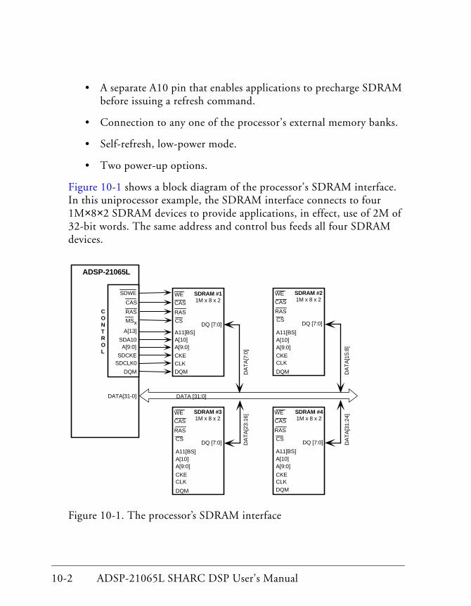
10-2 ADSP-21065L SHARC DSP User’s Manual
• A separate A10 pin that enables applications to precharge SDRAM before issuing a refresh command.
• Connection to any one of the processor’s external memory banks.
• Self-refresh, low-power mode.
• Two power-up options.
Figure 10-1 shows a block diagram of the processor’s SDRAM interface. In this uniprocessor example, the SDRAM interface connects to four 1M×8×2 SDRAM devices to provide applications, in effect, use of 2M of 32-bit words. The same address and control bus feeds all four SDRAM devices.
Figure 10-1. The processor’s SDRAM interface
DATA[31-0]
ADSP-21065L
MSx
RAS
CAS
DQM
SDWE
SDCLK0SDCKE
CONTROL
A[9:0]
A[13]
SDA10
RAS
CAS
DQM
WE
CLKCKE
SDRAM #11M x 8 x 2
A11[BS]DQ [7:0]
A[9:0]
CS
A[10]
DATA [31:0]
RAS
CAS
DQM
WE
CLKCKE
SDRAM #31M x 8 x 2
A11[BS]
DQ [7:0]
A[9:0]
CS
A[10]
RAS
CAS
DQM
WE
CLKCKE
SDRAM #21M x 8 x 2
A11[BS]
DQ [7:0]
A[9:0]
CS
A[10]
RAS
CAS
DQM
WE
CLKCKE
SDRAM #41M x 8 x 2
A11[BS]
DQ [7:0]
A[9:0]
CS
A[10]
DA
TA
[15:
8]D
AT
A[3
1:24
]
DA
TA
[7:0
]D
AT
A[2
3:16
]

ADSP-21065L SHARC DSP User’s Manual 10-3
SDRAM Interface
Figure 10-2 shows another uniprocessor example in which the SDRAM interface connects to multiple banks of SDRAM to provide 512M of SDRAM in ×4 I/O configuration, which results in 16M × 32-bit words. In this example, OxA and OxB output from the registered buffers are the same signal, but buffered separately. In the registered buffers, a delay of one clock cycle occurs between input (Ix) and its corresponding output (OxA or OxB).
Figure 10-2. Uniprocessor system with multiple SDRAM devices
DATA[31-0]
ADSP-21065L
MS3
RAS
CAS
DQM
SDWE
SDCLK0
SDCKE
CONTROL
A[13:11]
A[9:0]
SDA10
SDCLK1
RegisteredBuffers
I0
I5
I4
I3
I2
I1
O0A
O5A
O4A
O3A
O2A
O1A
O0B
O5B
O4B
O3B
O2B
O1B
Ix[13:0] Oxa[13:0]
Oxb[13:0]
RAS
CAS
DQM
WE
CLKCKE
SDRAM #14M x 4 x 4
DATA [3:0]
A[13:0]CS
RAS
CAS
DQM
WE
CLKCKE
SDRAM #34M x 4 x 4
DATA [3:0]
A[13:0]CS
RAS
CAS
DQM
WE
CLKCKE
SDRAM #24M x 4 x 4
DATA [3:0]
A[13:0]CS
RAS
CAS
DQM
WE
CLKCKE
SDRAM #44M x 4 x 4
DATA [3:0]
A[13:0]CS
RAS
CAS
DQM
WE
CLKCKE
SDRAM #84M x 4 x 4
DATA [3:0]
A[13:0]CS
RAS
CAS
DQM
WE
CLK
CKE
SDRAM #64M x 4 x 4
DATA [3:0]
A[13:0]CS
RAS
CAS
DQM
WE
CLKCKE
SDRAM #74M x 4 x 4
DATA [3:0]
A[13:0]CS
RAS
CAS
DQM
WE
CLK
CKE
SDRAM #54M x 4 x 4
DATA [3:0]
A[13:0]CS
Ab[13:0]
Aa[13:0]
[23:20]
[27:24]
[31:28]
[7:4]
[15:12]
[11:8]
[19:16][3:0]
Ab[13:0]
D Q
D Q
Addr [14]
Ctrl [6]
20
20 SDRAM Bank 1Addr & Ctrl
SDRAM Bank 2Addr & Ctrl

10-4 ADSP-21065L SHARC DSP User’s Manual
Table 10-1 lists and describes the processor’s SDRAM pins and their connections.
Table 10-1. SDRAM pin connections
Pin Type Description
CAS I/O/Z SDRAM Column Address Select pin. Connect to SDRAM’s CAS buffer pin.
DQM O/Z SDRAM Data Mask pin. Connect to SDRAM’s DQM buffer pin.
The processor drives this pin high during reset, until SDRAM is started.
MSx O/Z Memory select lines of external memory bank configured for SDRAM. Connect to SDRAM’s CS (chip select) pin.
RAS I/O/Z SDRAM Row Address Select pin. Connect to SDRAM’s RAS pin.
SDA10 O/Z SDRAM A10 pin. SDRAM interface uses this pin to retain control of the SDRAM device during host bus requests. Connect to SDRAM’s A10 pin
SDCKE I/O/Z SDRAM Clock Enable pin. Connect to SDRAM’s CKE pin.
SDCLK0 O/S/Z SDRAM SDCLK0 output pin. Connect to the SDRAM’s CLK pin.
SDCLK1 O/S/Z SDRAM SDCLK1 output pin. Connect to the SDRAM’s CLK pin.
SDWE I/O/Z SDRAM Write Enable pin. Connect to SDRAM’s WE or W buffer pin.
I = Input; O = Output; S = Synchronous; Z = Hi-Z
ADSP-21065L SHARC DSP User’s Manual 10-5
SDRAM Interface
The following terms are used throughout this chapter:
Bank Activate commandActivates the selected bank and latches in a new row address. It must be applied before a read or write command.
Burst lengthDetermines the number of words the SDRAM inputs or outputs after detecting a write or read command, respectively.
The processor supports full-page mode only.
During a full-page burst cycle, the SDRAM generates all subse-quent addresses internally by incrementing the column address sequentially.
See also, page size.
Burst Stop commandOne of several ways to terminate a burst read or write operation.
Terminates the current burst operation, but leaves the bank open for future reads or writes to the same page of the active bank.
Burst typeDetermines the order in which the SDRAM delivers or stores burst data after detecting a read or write command, respectively.
The processor supports sequential accesses only.
CAS latency (also tAA, tCAC, CL)The delay, in clock cycles, between when the SDRAM detects the read command and when it provides the data at its output pins.
The speed grade of the device and the application’s clock frequency determine the value of the CAS latency.

10-6 ADSP-21065L SHARC DSP User’s Manual
The application must program the CAS latency value into the IOCTL register after power up.
CBR Automatic refresh (CAS before RAS) mode.
In this mode, the SDRAM drives its own refresh cycle with no external control input. At cycle end, all SDRAM banks are pre-charged (idle).
DQM Data I/O Mask function.
Asserted during a precharge command or when a burst stop com-mand interrupts a burst write.
When asserted during a write cycle, this signal interrupts and dis-ables the write operation immediately.
IOCTL registerIOP register that contains programmable SDRAM control and configuration parameters that support different vendor’s timing and power-up sequence requirements.
Mode registerThe SDRAM’s configuration register that contains user-defined parameters (corresponds to the processor’s IOCTL register). After initial power-up and before executing a read or write command, the application must program the Mode register.
Page sizeThe size, in words, of the SDRAM’s page. The processor supports 1024-, 512-, and 256-word page sizes.
For 128M SDRAM devices with 2K page size, the SDRAM con-troller stops the burst after the first 1K words.
Programmable option in the IOCTL register.

ADSP-21065L SHARC DSP User’s Manual 10-7
SDRAM Interface
Precharge commandPrecharges (closes) an active bank.
SDRDIVProgrammable Refresh Counter.
An IOP register containing a refresh counter value.
Clock supplied to the SDRAM can vary between 20 and 60MHz. This counter enables applications to coordinate CLK rate with the SDRAM’s required refresh rate.
Self-RefreshThe SDRAM’s internal timer initiates automatic refresh cycles periodically, without external control input. Places the SDRAM device in a low-power mode.
Programmable option in the IOCTL register.
tRAS Active Command time.
Required delay between issuing an activate command and issuing a precharge command. A vendor-specific value.
Programmable option in the IOCTL register.
tRC Bank Cycle time.
Required delay between successive Bank Activate commands to the same bank. A vendor-specific value. Equal to tRP+tRAS.
The processor fixes the value of this parameter, so it is a nonpro-grammable option.
10-8 ADSP-21065L SHARC DSP User’s Manual
tRCD RAS to CAS delay.
Required delay between a Bank Activate command and the start of the first read or write operation. A vendor-specific value. Equal to CAS latency.
The processor fixes the value of this parameter, so it is a nonpro-grammable option.
tRP Precharge time.
Required delay between issuing a precharge command and issuing an activate command. A vendor-specific value.
Programmable option in the IOCTL register.

ADSP-21065L SHARC DSP User’s Manual 10-9
SDRAM Interface
SDRAM Control Register (IOCTL)SDRAMs are available from several vendors—IBM, Micron Electronics, Texas Instruments, and others. Each vendor has different requirements for the power-up sequence and timing parameters—tRAS (Active to Precharge command delay) and tRP (Precharge to Active command delay)—for their SDRAM product.
To support multiple vendors, the processor’s IOCTL register, shown in Figure 10-3 on page 10-12, contains programmable SDRAM control bits. The IOCTL register is an I/O processor register, which does not support bitwise operations.
To meet your SDRAM’s particular requirements, set the corresponding IOCTL control bits accordingly, as shown in Table 10-2. The IOP address of the IOCTL register is 0x2E.
Table 10-2. IOCTL control bits
Bit Name Description
10 DSDCTL Disable SDCLK0, RAS, CAS, SDWE, DQM, SDCKE.
Disables all SDRAM signals.
0= enable
1= disable
11 DSDCK1 Disable SDCLK1.
Disables SDCLK1 signal only.
0= enable
1= disable

SDRAM Control Register (IOCTL)
10-10 ADSP-21065L SHARC DSP User’s Manual
12-14 SDPGS SDRAM page size.
000=1024 words
001=512 words
010=256 words
others = reserved
15 SDSRF SDRAM self-refresh mode.
0= disable
1= enable
This control bit always reads zero (0).
16-17 SDCL SDRAM CAS latency.
Sets the delay, in number of clock cycles, between the time the SDRAM detects the read command and the time the data is available at its outputs.
01= 1 cycle
10= 2 cycles
11= 3 cycles
18-20 SDTRAS SDRAM tRAS spec in number of clock cycles.
21-23 SDTRP SDRAM, tRP spec in number of clock cycles.
24 SDPM SDRAM power-up option.
Specifies the sequence of commands in the SDRAM power-up cycle.
0= precharge, 8 CBR ref, mode reg set
1= precharge, mode reg set, 8 CBR ref
Table 10-2. IOCTL control bits (Cont’d)
Bit Name Description

ADSP-21065L SHARC DSP User’s Manual 10-11
SDRAM Interface
25-27 SDBS SDRAM Bank select.
Specifies the processor’s external memory bank to which the SDRAM connects.
000=no SDRAM
100=bank0
101=bank1
110=bank2
111=bank3
28 SDBUF SDRAM Buffer.
Enables/disables pipelining of address and control signals when using external buff-ering between the processor and SDRAM. Supports multiple SDRAMs connected in par-allel.
0= disable
1= enable
29-30 SDBN SDRAM number of banks.
Specifies the number of banks the SDRAM contains.
00= 2 banks
01= 4 banks
1x= reserved
31 SDPSS Start SDRAM power up sequence.
Write 1 to initiate power up sequence. SDPSS always reads as 0.
Table 10-2. IOCTL control bits (Cont’d)
Bit Name Description

SDRAM Control Register (IOCTL)
10-12 ADSP-21065L SHARC DSP User’s Manual
See Chapter 11‚ Programmable Timers and I/O Ports, for the definition of bits 7:0.
Figure 10-3. IOCTL Register Definition
0 0 00000 00000000 0
31 30 29 28 27 26 25 24 23 22 21 20 19 18 17 16
SDCLSDRAMCAS Latency01=1 clk cycle10=2 clk cycles11=3 clk cycles
SDTRPSDRAM tRP Spec.(# clk cycles)
SDTRASSDRAM tRAS Spec.(# clk cycles)
SDPMSDRAMPower Up Mode0=prechg, 8 CBR refs., mode reg set1=prechg, mode reg. set, 8 CBR refs.
SDPSSSDRAM
Power Up Seq.Write 1 to start
SDBNSDRAM
# of banks00=2 banks01=4 banks
1x=reserved
SDBUFExt. SDRAM
ctrl/addr Buffer0=No buffer
1=With buffer
SDBSSDRAM Ext.Bank Select
000=None100=Bank 0101=Bank 1110=Bank 2111=Bank 3
0 0 00000 00000000 0
15 14 13 12 11 10 9 8 7 6 5 4 3 2 1 0
SDSFRSDRAM
Self-Refresh0=disable1=enable
SDPGSSDRAM Page Size
000=1024 words001=512 words010=256 words
others=reserved
FLG6O
DSDCK1SDCLK1 Disable
0=enable1=disable
DSDCTLSDCLK0 Disable0=enable1=disable
FLG7O
FLG4OGen. Purpose I/OUser-defined0=input1=output
FLG8O
FLG5O
FLG11O
FLG10O
FLG9O
ADSP-21065L SHARC DSP User’s Manual 10-13
SDRAM Interface
Configuring SDRAM OperationThe processor’s IOCTL register stores the configuration of the SDRAM interface. Writing some configuration parameters initiates commands that take effect immediately.
Before starting the SDRAM power-up sequence, your application must write all of the SDRAM configuration parameter values to the IOCTL register, and, at initial power-up, set the SDRDIV register.
In the SDRDIV register, a memory-mapped IOP register, you set the value for the SDRAM refresh counter.
In the IOCTL register, you program the parameter bits to:
• Set the SDRAM clock enables (DSDCTL and DSDCK1).
• Select the number of banks the SDRAM contains (SDBN).
• Select the external memory bank configured for and connected to the SDRAM (SDBS).
• Set the SDRAM buffering option (SDBUF).
• Select the CAS latency value (SDCL).
• Select the SDRAM page size (SDPGS).
• Select the SDRAM power-up mode (SDPM).
• Start the SDRAM power-up sequence (SDPSS).
• Start SDRAM self-refresh mode (SDSRF).
• Set the Active Command delay (SDTRAS).
• Set the Precharge delay (SDTRP).
Configuring SDRAM Operation
10-14 ADSP-21065L SHARC DSP User’s Manual
Setting the Refresh Counter Value (SDRDIV)Since the clock supplied to the SDRAM can vary between 20MHz and 60MHz, the processor provides a programmable refresh counter, SDRDIV, to coordinate the supplied clock rate with the SDRAM device’s required refresh rate.
Your application must write to SDRDIV the delay, in number of clock cycles, that must occur between consecutive refresh commands.
To calculate the value of the refresh counter for which to program the SDRDIV register, use this equation:
Where:
CL= CAS latency programmed in the IOCTL register.
tRP= tRP spec programmed in the IOCTL register.
For example, for an IBM SDRAM with:
Ref. rate= 4096 cycles/64ms.
CLKIN= 33 MHz
CL= 2
tRP= 2
Write this value to the SDRDIV register before writing the SDRAM parameter values to the IOCTL register.
SDRDIV= [(2 x fCLKIN)/(SDRAM refresh rate)] −CL −tRP −4

ADSP-21065L SHARC DSP User’s Manual 10-15
SDRAM Interface
The equation yields:
[(2x30x(106))/(4096/64x(10−3))]−2−2−4 = 930 (decimal)
Setting the SDRAM Clock Enables(DSDCTL and DSDCK1)
Systems with several SDRAM devices connected in parallel that require buffering between the processor and multiple SDRAM devices may also generate increased clock loads.
To meet higher clock load requirements, the processor provides two SDRAM clock control pins, SDCLK0 and SDCLK1. These pins eliminate the need for off-chip clock buffers.
The DSDCTL and DSDCK1 bits in the IOCTL register provide control for the SDRAM clock control pins.
The DSDCTL bit enables you to Hi-Z all of the SDRAM control pins DQM, CAS, RAS, SDWE, and SDCKE and the SDCLK0 pin:
DSDCTL=0 Enable all SDRAM control pins.
DSDCTL=1 Disable all SDRAM control pins.
The DSDCK1 bit enables you to Hi-Z the SDCLK1 pin only:
DSDCK1=0 Enable SDCLK1.
DSDCK1=1 Disable SDCLK1.
If your system does not use SDRAM, set both DSDCTL and DSDCK1 to 1.
If your system uses SDRAM, but the clock load is minimal, set DSDCTL to 0 and DSDCK1 to 1 This setting enables the SDCLK0 pin and all related SDRAM control pins, but disables (puts in Hi-Z) the second clock pin SDCLK1.

Configuring SDRAM Operation
10-16 ADSP-21065L SHARC DSP User’s Manual
If your system uses SDRAM and the clock load is heavy—such as a system using registered buffers and eight ×4 SDRAMs to get ×32-bit data—set both DSDCTL and DSDCK1 to 0. This setting enables SDCLK0, SDCLK1, and all SDRAM control pins. In this configuration, SDCLK0 and SDCLK1 can each share half of the clock load. See Figure 10-2 on page 10-3.
Setting the Number of SDRAM Banks (SDBN)The SDBN bit defines for the processor’s SDRAM controller the number of banks your SDRAM device contains.
The SDRAM controller uses this value and the value you assign to the SDPGS (page size) bit to map the address bits on the processor’s internal 32-bit address (DMA/PMA/EPA) bus into SDRAM column address, row address, and bank select address.
The SDBN bits in the IOCTL register select the number of banks the SDRAM contains:
SDBN=00 2 banks.
SDBN=01 4 banks.
SDBN=1x Reserved.
Setting the External Memory Bank (SDBS)When you use SDRAM, you must connect its CS line to one of the pro-cessor’s external memory banks MS3-0 and, in the IOCTL register, configure that bank for SDRAM operation.
ADSP-21065L SHARC DSP User’s Manual 10-17
SDRAM Interface
The SDBS bits in the IOCTL register configure one of the processor’s external memory banks for SDRAM operation:
SDBS=000 No SDRAM.
SDBS=100 Bank 0.
SDBS=101 Bank 1.
SDBS=110 Bank 2.
SDBS=111 Bank 3.
Setting the SDRAM Buffering Option (SDBUF)To meet overall system timing requirements, systems that employ several SDRAM devices connected in parallel may require buffering between the processor and multiple SDRAM devices.
To meet such timing requirements and enable intermediary buffering, the processor supports pipelining of SDRAM address and control signals.
The pipeline bit SDBUF in the IOCTL register enables this mode:
SDBUF=0 Disable pipelining.
SDBUF=1 Enable pipelining.
Make sure your application programs a zero (0) wait state for the external memory bank to which the SDRAM device maps. That is, set EBxWS=000 in the WAIT register.
You cannot use external handshake and paced master mode DMA on the external memory bank to which you map an SDRAM device.

Configuring SDRAM Operation
10-18 ADSP-21065L SHARC DSP User’s Manual
When SDBUF=1, the SDRAM controller delays the data in write accesses one cycle, enabling the processor to latch the address and controls exter-nally. In read accesses, the SDRAM controller samples data one cycle later.
Selecting the CAS Latency Value (SDCL)The CAS latency value defines the delay, in number of clock cycles, between the time the SDRAM detects the read command and provides the data at its output pins. This parameter enables your application to match SDRAM operation with the processor’s ability to latch the data output.
CAS latency does not apply to write cycles.
The SDCL bits in the IOCTL register select the CAS latency value:
SDCL=01 1 clock cycle.
SDCL=10 2 clock cycles.
SDCL=11 3 clock cycles.
Generally, the frequency of the operation determines the value of the CAS latency. For more details, see the documentation that accompanied your SDRAM device.
Selecting the SDRAM’s Page Size (SDPGS)The processor supports full-page burst length only. The SDPGS bit defines for the processor’s SDRAM controller the page size, in number of words, of the SDRAM’s banks.
The SDRAM controller uses this value and the value you assign to the SDBN (number of banks) bit to map the address bits on the processor’s internal 32-bit address (DMA/PMA/EPA) bus into SDRAM column address, row address, and bank select address.
ADSP-21065L SHARC DSP User’s Manual 10-19
SDRAM Interface
Page length depends on the I/O organization and column addressing of the SDRAM’s internal banks. For example, a 16Mb SDRAM organized as 2 M × 4 I/O × 2 Banks has a page size of 1024 words.
The SDPGS bits in the IOCTL register select the SDRAM page length:
SDPGS=000 1024 words.
SDPGS=001 512 words.
SDPGS=010 256 words.
All other values are reserved.
Setting the SDRAM Power-Up Mode (SDPM)To avoid unpredictable start-up modes, SDRAM devices must follow a specific initialization sequence during power up. The processor provides two commonly used power-up options. This parameter enables your application to accommodate power-up requirements of your SDRAM.
The SDPM bit in the IOCTL register selects the SDRAM power-up mode:
SDPM=0 The SDRAM controller issues, in this order:A precharge commandEight CBR refresh cyclesAn MRS (Mode Register Set) command
SDPM=1 The SDRAM controller issues, in this order:A precharge commandAn MRS (Mode Register Set) commandEight CBR refresh cycles
For details, see the documentation that accompanied your SDRAM device.

Configuring SDRAM Operation
10-20 ADSP-21065L SHARC DSP User’s Manual
Starting the SDRAM Power-Up Sequence (SDPSS)Before starting the power-up sequence, your application must write the IOCTL register to configure the SDRAM parameters. Whenever it does, your application must write to all of the register bits, regardless of the number of parameter values that will not change.
To start the SDRAM power-up sequence, you write a 1 to the SDPSS bit in the IOCTL register. The initialization sequence executed during power-up depends on the value of the SDPM bit (page 10-19).
The SDPSS bit always reads as zero (0).
For more details, see the documentation that accompanied your SDRAM device.
Starting Self-Refresh mode (SDSRF)The processor supports SDRAM self-refresh mode. In self-refresh mode, the SDRAM performs refresh operations internally, without external con-trol, reducing the SDRAM’s power consumption
The SDSRF bit in the IOCTL register enables and disables the self-refresh option:
SDSRF=0 Disable self-refresh mode.
SDSRF=1 Enable self-refresh mode.
Make sure your application initializes the SDRDIV register before it starts the power-up sequence. After power up, make sure it waits one cycle before it writes the IOCTL register to issue another SDRAM command.
ADSP-21065L SHARC DSP User’s Manual 10-21
SDRAM Interface
When SDSRF=1, the processor’s SDRAM controller issues a Sref command to the SDRAM device or devices, putting them into self-refresh mode immediately. For details, see “Sref (Self-Refresh)” on page 10-39.
Selecting the Active Command Delay (SDTRAS)The tRAS value (Active Command delay) defines the required delay, in number of clock cycles, between the time the SDRAM controller issues a Bank Activate command and the time it issues a Precharge command.
This parameter enables your application to accommodate your SDRAM’s timing requirements.
The SDTRAS bits in the IOCTL register select the tRAS value. For example:
SDTRAS=001 1 clock cycle.
SDTRAS=010 2 clock cycles.
SDTRAS=111 7 clock cycles.
For more details, see the documentation that accompanied your SDRAM device.
Selecting the Precharge Delay (SDTRP)The tRP value (Precharge delay) defines the required delay, in number of clock cycles, between the time the SDRAM controller issues a Precharge command and the time it issues a Bank Activate command.
This parameter enables your application to accommodate your SDRAM’s timing requirements.

Configuring SDRAM Operation
10-22 ADSP-21065L SHARC DSP User’s Manual
The SDTRP bits in the IOCTL register select the tRP value. For example:
SDTRP=001 1 clock cycle.
SDTRP=010 2 clock cycles.
SDTRP=111 7 clock cycles.

ADSP-21065L SHARC DSP User’s Manual 10-23
SDRAM Interface
SDRAM Controller OperationFor page read and write operations, the processor’s SDRAM controller programs the SDRAM device for full page burst length. Since all SDRAM devices can terminate an active burst sequence and start a new one, the SDRAM controller issues all commands to support this operation.
For page read and write operations, the SDRAM starts the access at the column address defined at the beginning of the cycle in the ADDR bits.
Table 10-3 lists the data throughput rates for the processor’s core or DMA read/write accesses to SDRAM. All clock cycles are 2xCLKIN and these data assume:
• CAS latency = 2 cycles (SDCL=2)
• No SDRAM buffering (SDBUF=0)
• RAS precharge (tRP) = 2 cycles (SDTRP=2)
• Active command time (tRAS) = 3 cycles (SDTRP=3).
Table 10-3. Throughput for core or DMA read/write operations
Accesses Operations Page Throughput per 2xCLKIN (32-bit words)1, 2
Sequential, uninterrupted
Read Same 1 word/1 cycle
Sequential, uninterrupted
Write Same 1 word/1 cycle
Nonsequential,uninterrupted
Read Same 1 word/4 cycles(CL+2)
tRAS = Active to precharge time; tRP = Precharge time; CL = CAS latency

SDRAM Controller Operation
10-24 ADSP-21065L SHARC DSP User’s Manual
DMA OperationFor DMA mode data transfers to or from SDRAM, one full page can be accessed at full throughput if the external address incrementor = 1. If the external address incrementor is >1, one full page can be written at full throughput, but reads incur overhead.
Nonsequential, uninterrupted
Write Same 1 word/1 cycle
Both Alternating
read/write
Same Average rate = 2.5 cycles per word (reads = 4 cycles; writes = 1 cycle)
Nonsequential Reads Different 1 word/8 cycles
(tRP +2CL+2)
Nonsequential Writes Different 1 word/5 cycles
(tRP +CL+1)
Autorefresh before read
Reads Different 1 word/13 cycles
(2tRP +tRAS +2CL+2)
Autorefresh before write
Writes Different 1 word/10 cycles
(2tRP +tRAS +CL+1)
1 For 48-bit words, add one clock cycle to the throughput value or to the average access rate.2 With SDRAM buffering enabled (SDBUF=1), replace any instance of (CL) with (CL+1)..
Table 10-3. Throughput for core or DMA read/write operations
Accesses Operations Page Throughput per 2xCLKIN (32-bit words)1, 2
tRAS = Active to precharge time; tRP = Precharge time; CL = CAS latency

ADSP-21065L SHARC DSP User’s Manual 10-25
SDRAM Interface
When a page miss occurs, before executing the read/write command, the SDRAM controller executes a Burst Stop command followed by a Pre-charge and a Bank Activate command.
For an SDRAM read, a latency (equal to CAS latency) exists from the start of the read command until data is available from the SDRAM. For the first read in a sequence of reads, the latency will always exist. Subsequent reads will not have a latency if the address is sequential and uninterrupted.
Multiprocessing OperationIn a multiprocessing environment, both processors share the SDRAM. While the bus master always drives SDRAM input signals (including clock), the slave processor tracks the commands the master processor issues to the SDRAM. This tracking helps to synchronize the SDRAM refresh counters and to avoid needless refreshing operations.
When one processor receives bus mastership from the other, it executes a Precharge command before its first access to SDRAM only if the previous master had accessed SDRAM. The application must initialize the relevant bits in the IOCTL and SDRDIV registers of both processors to the same values.
If the system uses no SDRAM (as indicated in IOCTL), bus transition proceeds normally (see Chapter 7, Multiprocessing).
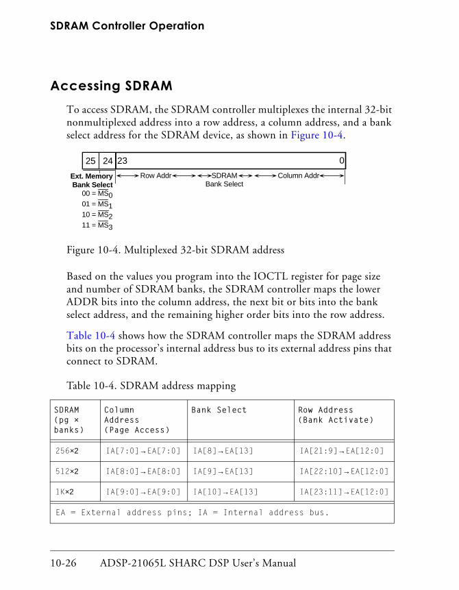
SDRAM Controller Operation
10-26 ADSP-21065L SHARC DSP User’s Manual
Accessing SDRAMTo access SDRAM, the SDRAM controller multiplexes the internal 32-bit nonmultiplexed address into a row address, a column address, and a bank select address for the SDRAM device, as shown in Figure 10-4.
Figure 10-4. Multiplexed 32-bit SDRAM address
Based on the values you program into the IOCTL register for page size and number of SDRAM banks, the SDRAM controller maps the lower ADDR bits into the column address, the next bit or bits into the bank select address, and the remaining higher order bits into the row address.
Table 10-4 shows how the SDRAM controller maps the SDRAM address bits on the processor’s internal address bus to its external address pins that connect to SDRAM.
Table 10-4. SDRAM address mapping
SDRAM(pg × banks)
Column Address(Page Access)
Bank Select Row Address(Bank Activate)
256×2 IA[7:0]→EA[7:0] IA[8]→EA[13] IA[21:9]→EA[12:0]
512×2 IA[8:0]→EA[8:0] IA[9]→EA[13] IA[22:10]→EA[12:0]
1K×2 IA[9:0]→EA[9:0] IA[10]→EA[13] IA[23:11]→EA[12:0]
EA = External address pins; IA = Internal address bus.
23
Column AddrRow Addr
025 24
SDRAMBank Select
Ext. MemoryBank Select
00 = MS001 = MS110 = MS211 = MS3
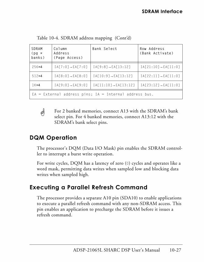
ADSP-21065L SHARC DSP User’s Manual 10-27
SDRAM Interface
DQM OperationThe processor’s DQM (Data I/O Mask) pin enables the SDRAM control-ler to interrupt a burst write operation.
For write cycles, DQM has a latency of zero (0) cycles and operates like a word mask, permitting data writes when sampled low and blocking data writes when sampled high.
Executing a Parallel Refresh CommandThe processor provides a separate A10 pin (SDA10) to enable applications to execute a parallel refresh command with any non-SDRAM access. This pin enables an application to precharge the SDRAM before it issues a refresh command.
256×4 IA[7:0]→EA[7:0] IA[9:8]→EA[13:12] IA[21:10]→EA[11:0]
512×4 IA[8:0]→EA[8:0] IA[10:9]→EA[13:12] IA[22:11]→EA[11:0]
1K×4 IA[9:0]→EA[9:0] IA[11:10]→EA[13:12] IA[23:12]→EA[11:0]
For 2 banked memories, connect A13 with the SDRAM’s bank select pin. For 4 banked memories, connect A13:12 with the SDRAM’s bank select pins.
Table 10-4. SDRAM address mapping (Cont’d)
SDRAM(pg × banks)
Column Address(Page Access)
Bank Select Row Address(Bank Activate)
EA = External address pins; IA = Internal address bus.
SDRAM Controller Operation
10-28 ADSP-21065L SHARC DSP User’s Manual
Connecting this pin to the SDRAM’s A10 line and using it, instead of ADDR10, to precharge the SDRAM device enables the processor to retain control of the SDRAM device while a host requests and controls the exter-nal ADDR23-0 bus.
Entering and Exiting Self-Refresh ModeWriting 1 to the SDSRF bit in the IOCTL register causes the SDRAM controller to issue a Sref command to the SDRAM device. When the Sref command is issued depends on whether or not the processor’s core or DMA controller is engaged in an external SDRAM access.
If no external SDRAM access is in progress, the SDRAM controller issues the Sref command immediately. Otherwise, it delays issuing the Sref com-mand until the processor’s core or DMA controller completes its current SDRAM access and any subsequent access requests.
Once the SDRAM device enters into self-refresh mode, the SDRAM con-troller resets the SDSRF bit in the IOCTL register. The SDSRF bit always reads as 0, regardless of a pending request. The SDRAM controller ignores another self-refresh request (SDSRF=1) when the SDRAM device is already in self-refresh mode.
The application cannot clear the SDSRF bit (SDSRF=0) to cancel self-refresh mode. The SDRAM device exits self-refresh mode only when it receives a core or DMA access request from the SDRAM controller.
Powering Up After ResetAfter reset, once the application has written the IOCTL register, the con-troller initiates the power-up sequence. The SDPM bit of the IOCTL register determines the exact sequence. In a multiprocessing environment, either processor initiates the power-up sequence. A software reset does not reset the controller and will not reinitiate a power-up sequence.
ADSP-21065L SHARC DSP User’s Manual 10-29
SDRAM Interface
SDRAM Controller CommandsThis section provides a description of each of the commands the proces-sor’s on-chip SDRAM controller uses to manage the SDRAM interface. These commands are transparent to applications.
The SDRAM commands are:
• Act (bank activate)
Activates a page in the required bank.
• Bstop (burst stop)
Terminates the currently executing burst read or write operation.
• MRS (mode register self-refresh)
Initializes the SDRAM operation parameters during the power-up sequence.
• Pre (precharge)
Precharges the active bank.
• Read/write
• Ref (refresh)
Causes the SDRAM to enter refresh mode and generate all addresses internally.
• Sref (self-refresh)
Places the SDRAM in self-refresh mode, in which it controls its refresh operations internally.

SDRAM Controller Commands
10-30 ADSP-21065L SHARC DSP User’s Manual
• NOP (no operation)
If a read or write is followed by a NOP, the SDRAM will start the full page burst.
Act (Bank Activate) A Bank Activate command is required if the next data access is in a differ-ent page.
The SDRAM controller executes a Pre command followed by an Act com-mand to activate the page in the required bank. Only one bank at a time can be active.
The SDRAM pin state during the Act command is:
Bstop (Burst Stop)A Burst Stop command terminates the currently executing burst read or burst write operation prematurely, but leaves the bank open for future reads or writes to the same page of the active bank.
Pin State
MSx1
1 X = One of the processor’s external mem-ory banks configured for SDRAM.
Low
CAS High
RAS Low
SDWE High
SDCKE High

ADSP-21065L SHARC DSP User’s Manual 10-31
SDRAM Interface
The SDRAM pin state during the Bstop command is:
MRS (Mode Register Set)Part of the power-up sequence. Initializes the SDRAM operation parameters.
MRS uses SDRAM address bits A0-A13 as data input.
To start the power-up sequence, you write 1 to the SDPSS bit in the IOCTL register. The SDPM bit specifies the exact sequence of commands The SDRAM controller uses in the power-up procedure.
MRS initializes the following parameters:
• Burst length Full page; bits 2:0; fixed in processor.
• Burst type Sequential; bit 3; fixed in processor.
Pin State
MSx1
1 X = One of the processor’s external mem-ory banks configured for SDRAM.
Low
CAS High
DQM High (write only)
RAS High
SDWE Low
SDCKE High
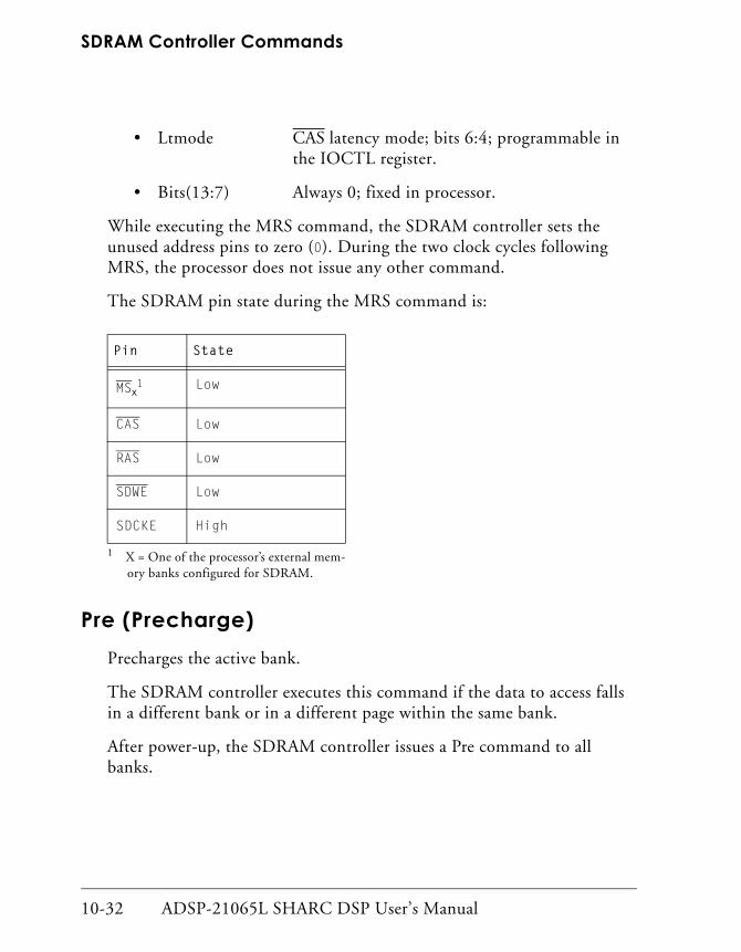
SDRAM Controller Commands
10-32 ADSP-21065L SHARC DSP User’s Manual
• Ltmode CAS latency mode; bits 6:4; programmable inthe IOCTL register.
• Bits(13:7) Always 0; fixed in processor.
While executing the MRS command, the SDRAM controller sets the unused address pins to zero (0). During the two clock cycles following MRS, the processor does not issue any other command.
The SDRAM pin state during the MRS command is:
Pre (Precharge)Precharges the active bank.
The SDRAM controller executes this command if the data to access falls in a different bank or in a different page within the same bank.
After power-up, the SDRAM controller issues a Pre command to all banks.
Pin State
MSx1
1 X = One of the processor’s external mem-ory banks configured for SDRAM.
Low
CAS Low
RAS Low
SDWE Low
SDCKE High

ADSP-21065L SHARC DSP User’s Manual 10-33
SDRAM Interface
The SDRAM pin state during the Pre command is:
Read/WriteThe SDRAM controller executes a Read/Write command if the next read/write data falls in the currently active page.
Read Commands
For the Read command, the SDRAM controller asserts the CAS, MSx, and SDA10 pins to enable the SDRAM to latch the column address. The column address determines the burst start address.
Figure 10-5 shows an example timing of a read command that reads four sequential addresses and terminates with a burst stop (Bstop) command. The tRCD parameter determines the delay between Act and Read com-mands. Data is available after the tRCD and CAS latency requirements are met.
Pin State
MSx1
1 X = One of the processor’s external mem-ory banks configured for SDRAM.
Low
CAS High
RAS Low
SDWE Low
SDCKE High
SDA10 High

SDRAM Controller Commands
10-34 ADSP-21065L SHARC DSP User’s Manual
Figure 10-5. Example timing of a read command
The SDRAM pin state during the Read command is:
Pin State
MSx1 Low
CAS Low
RAS High
SDWE High
SDCKE High
SDA10 Low
+ % .-+ + + + + + +
% % % %
% % % %
% % % %
0$!B
$"
$%# 78
$B,=G
$%# 78
$B,=G
$%# 78
$B,=G
) ( /
$
? 78$%# 7H
H
+
+
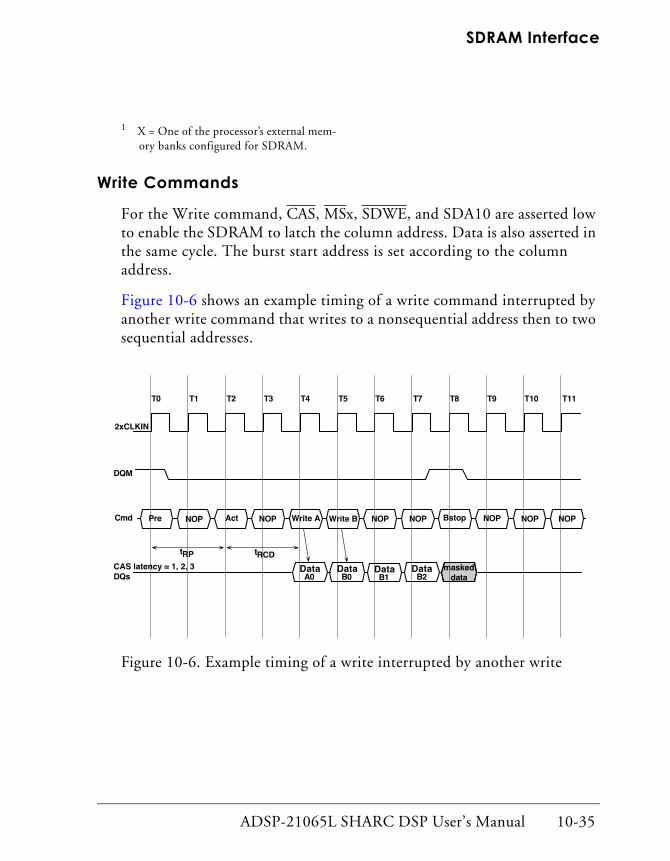
ADSP-21065L SHARC DSP User’s Manual 10-35
SDRAM Interface
Write Commands
For the Write command, CAS, MSx, SDWE, and SDA10 are asserted low to enable the SDRAM to latch the column address. Data is also asserted in the same cycle. The burst start address is set according to the column address.
Figure 10-6 shows an example timing of a write command interrupted by another write command that writes to a nonsequential address then to two sequential addresses.
Figure 10-6. Example timing of a write interrupted by another write
1 X = One of the processor’s external mem-ory banks configured for SDRAM.
+ % C% .-+ + +C. + + + +
% . .
.
" E
0$!B
$"
$%# 78==
G
G
) ( /
$+
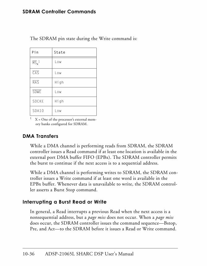
SDRAM Controller Commands
10-36 ADSP-21065L SHARC DSP User’s Manual
The SDRAM pin state during the Write command is:
DMA Transfers
While a DMA channel is performing reads from SDRAM, the SDRAM controller issues a Read command if at least one location is available in the external port DMA buffer FIFO (EPBx). The SDRAM controller permits the burst to continue if the next access is to a sequential address.
While a DMA channel is performing writes to SDRAM, the SDRAM con-troller issues a Write command if at least one word is available in the EPBx buffer. Whenever data is unavailable to write, the SDRAM control-ler asserts a Burst Stop command.
Interrupting a Burst Read or Write
In general, a Read interrupts a previous Read when the next access is a nonsequential address, but a page miss does not occur. When a page miss does occur, the SDRAM controller issues the command sequence—Bstop, Pre, and Act—to the SDRAM before it issues a Read or Write command.
Pin State
MSx1
1 X = One of the processor’s external mem-ory banks configured for SDRAM.
Low
CAS Low
RAS High
SDWE Low
SDCKE High
SDA10 Low

ADSP-21065L SHARC DSP User’s Manual 10-37
SDRAM Interface
If a Write (on page) interrupts a burst Read in progress, the SDRAM con-troller asserts a Burst Stop command and waits until the external data bus is three-stated before it issues a Write command.
Either a Read or another Write (if it is nonsequential) or a Bstop inter-rupts a burst Write in progress. If the internal refresh counter asserts a refresh request, it delays any new access until the SDRAM controller exe-cutes a Ref command.
A special situation occurs when the CAS latency = 1 and the processor must perform this sequence of operations:
1. Page write to location xyz.
2. No SDRAM operation by the core or DMA controller.
3. Page read from location abc.
Normally, to perform this sequence, the SDRAM controller issues these commands:
4. Write
5. Bstop
6. Read
The burst stop command asserts DQM to mask write data within the burst stop cycle. But since the DQM standard is always DQM latency = 2, with CAS latency = 1 (SDCL=1), no data is available at the SDRAM output pins for the read.
To avoid this situation, the SDRAM controller inserts a NOP between a Burst Stop command and a Read command only when the CAS latency is 1 (SDCL=1):
1. Write
2. Bstop

SDRAM Controller Commands
10-38 ADSP-21065L SHARC DSP User’s Manual
3. NOP
4. Read
Ref (Refresh)Requests the SDRAM to perform a CBR (CAS before RAS) transaction. Ref causes the SDRAM to generate all addresses internally.
Before executing the Ref command, the SDRAM controller executes a Pre command to the active bank (after tRAS min). It executes the next Act command only after a minimum delay equal to tRC.
The SDRAM pin state during the Ref command is:
The IOP address of the SDRDIV register maps to 0x20.
Setting the Delay Between Ref Commands
You use the processor’s SDRDIV register to set the number of clock cycles between two Ref commands. Your application must program the SDRDIV register before it writes to the IOCTL register. The SDRAM
Pin State
MSx1
1 X = One of the processor’s external mem-ory bank s configured for SDRAM.
Low
CAS Low
RAS Low
SDWE High
SDCKE High
ADSP-21065L SHARC DSP User’s Manual 10-39
SDRAM Interface
controller makes an internal CBR Ref request to the SDRAM based on this value. Before servicing a refresh request, the SDRAM controller com-pletes a current burst. The master processor always executes a refresh command.
Multiprocessing Operation
In a multiprocessing environment, both processors share the SDRAM. While the bus master always drives SDRAM input signals (including clock), the slave processor tracks the commands the master processor issues to the SDRAM. This tracking helps to synchronize the SDRAM refresh counters and to avoid needless refreshing operations.
When one ADSP-21065L receives bus mastership from the other, it exe-cutes a Precharge command before its first access to SDRAM only if the previous master accessed SDRAM.
If the Ref request arrives from the refresh counter during a bus transition cycle, the new bus master immediately issues a Ref command. The new bus master is aware of the Ref request because the refresh counter runs on both processors. The refresh counters on both processors reload synchro-nously because the slave watches the external SDRAM control pins to see when the master has executed the refresh command.
The master processor retains mastership of the SDRAM control pins (RAS, CAS, SDWE, SDCKE, SDCLK, DQM, MSx, SDA10) when the host assumes control of the system bus—HBG is asserted. This enables the master processor to issue Ref commands as necessary.
Sref (Self-Refresh)The Sref command causes the SDRAM to perform refresh operations internally, without any external control. Before executing the Sref com-mand, the SDRAM precharges the active bank.
Writing a 1 to the SDSRF bit of the IOCTL register enables Sref mode.

SDRAM Controller Commands
10-40 ADSP-21065L SHARC DSP User’s Manual
The SDRAM controller automatically asserts an Sref exit cycle if an SDRAM access occurs during the Sref period. After executing a Sref exit command, the SDRAM controller waits for 2 + tRC cycles to execute a CBR (CAS before RAS) refresh cycle. After the CBR refresh command, the SDRAM controller waits for tRC number of cycles before executing a bank activate command.
To reduce system power demand, three cycles after entering SREF, the SDRAM controller holds SDCLKx low, and two cycles before exiting SREF, it restores SDCLKx.
The SDRAM pin state during the Sref command is:
For details on SDRAM controller operation on entry and exit from self-refresh mode, see “Entering and Exiting Self-Refresh Mode” on page 10-28.
Pin State
MSx1
1 X = One of the processor’s external mem-ory bank s configured for SDRAM.
Low2
2 The processor asserts MSx high for two cycles when exiting self-refresh mode.
CAS Low
RAS Low
SDWE High
SDCKE Low

ADSP-21065L SHARC DSP User’s Manual 10-41
SDRAM Interface
SDRAM Timing SpecificationsTo support key timing requirements and power-up sequences for different SDRAM vendors, the processor provides programmability for tRAS and tRP and a power-up sequence mode (see the IOCTL register bit definitions).
Your application must set, in the IOCTL register, the CAS latency based on the frequency of the operation. (For details, see your SDRAM vendor’s data sheet.)
For other parameters, the SDRAM controller assumes:
• Bank cycle time tRC = tRAS + tRP
• RAS to CAS delay tRCD = CAS latency
Bit definitions for the SYSCON register are shown in Figure 10-4 on page 10-26.

SDRAM Timing Specifications
10-42 ADSP-21065L SHARC DSP User’s Manual

ADSP-21065L SHARC DSP User’s Manual 11-1
11 PROGRAMMABLE TIMERS AND I/O PORTS
Figure 11-0.
Table 11-0.
Listing 11-0.
The processor has two identical timer blocks, each of which has two basic functions:
• Pulse Width Waveform Generation/ PWMOUT (PWMOUT mode)
• Pulse Width Count/Capture. (WIDTH_CNT mode)
You can configure the timer in either mode. The timer has one input/out-put pin—PWM_EVENTx. This pin functions as an output pin in the PWMOUT mode and as an input pin in the WIDTH_CNT mode. To implement these functions, each timer has three registers—TPERIODx, TPWIDTHx, and TCOUNTx.
All timer counters are 32-bits wide and use the processor’s 2xCLKIN internal clock, which evaluates to a maximum period of 71.5 sec
((232-1) * 16.67 ns internal clock cycles) for the timer count.
To enable or disable the timer, you set or clear the TIMENx bit in the MODE2 register. Figure 11-1 on page 11-2 shows the timer’s enable and disable timing.

11-2 ADSP-21065L SHARC DSP User’s Manual
Figure 11-1. Timer enable and disable timing
2xCLK
PWMOUT
2xCLKTCOUNT=M TCOUNT=
M+1TCOUNT=
M+1TCOUNT=
M+1
Timer Enable
Set TIMEN(MODE2)
TimerEnabled
TPERIOD = 0x4TPWIDTH = 0x2TCOUNT = 1
TCOUNT=xx TCOUNT=xx TCOUNT=1 TCOUNT=2 TCOUNT=4TCOUNT=3
Clear TIMEN(MODE2)
TimerDisabled
Timer Disable
ADSP-21065L SHARC DSP User’s Manual 11-3
Programmable Timers and I/O Ports
PWMOUT ModeIn PWMOUT mode, the PWM_EVENTx is an output pin. To select it, you set the PWMOUTx bit high in the MODE2 register. The registers TPERIODx and TPWIDTHx contain the values of the timer count period and PWM output pulse width respectively.
To avoid unpredictable results of the PWM_EVENTx signal:
• Initialize TPWIDTHx and TPERIODx before enabling the timer.
• Do not alter TPWIDTHx and TPERIODx while the timer is enabled.
• Make sure the value of TPWIDTHx is less than the value of TPERIODx.
When the timer is enabled in this mode, the PWM_EVENTx is pulled low each time the TCOUNTx (up counter) value equals the TPERIODx value, and it is pulled high when the TCOUNTx value equals the TPWIDTHx value. TCOUNTx is reset once to 0x0000 0001 when the timer is enabled and each time TCOUNTx reaches the TPERIODx value. See Figure 11-1 on page 11-2.
When TCOUNTx equals TPERIODx, a timer interrupt (if enabled) is generated, and the CNT_EXPx/CNT_OVFx bit in the STKY register is set. The CNT_EXPx/CNT_OVFx bit is a sticky bit, and software must reset it explicitly. At reset, its value is 0. Figure 11-2 shows the timer flow.

PWMOUT Mode
11-4 ADSP-21065L SHARC DSP User’s Manual
Figure 11-2. Timer Flow Diagram–PWMOUT Mode
Data Bus
RESET
TIMER_ENABLE
Set CNT_EXP bit
TPERIODx TPWIDTx
CLOCK
Yes
Interrupt
Set PWMOUNT High
Set PWMOUNT Low
PWM_EVENTx
Equal?
TCOUNTx
Yes
PWMOUTLogic
1
1
Equal?

ADSP-21065L SHARC DSP User’s Manual 11-5
Programmable Timers and I/O Ports
WIDTH_CNT ModeIn the WIDTH_CNT mode, the PWM_EVENTx is an input pin. To select this mode, you set the PWMOUTx bit low in the MODE2 register.
When enabled in this mode, the timer resets TCOUNTx to 0x0000 0001 when it detects the leading edge of the PWM_EVENTx pin and starts counting (increments).
When it detects the trailing edge, the timer captures the current value of the TCOUNTx into the TPWIDTHx register. At the leading edge, the timer transfers the current value of the TCOUNTx into the TPERIODx register. This timing, shown in Figure 11-3, assumes the leading edge is set as 0 → 1.
Figure 11-3. WIDTH_CNT mode timing
In this case, your software application can measure both the pulse width and the pulse period values, which are available in the TPWIDTHx and the TPERIODx registers, respectively.
0x00000001 0x00000002 0x00000003 0x00000001
2xCLK
PWM_EVENT
1st LeadingEdge
Detected
FramingEdge
Detected
TCOUNT
2nd LeadingEdge
Detected
Transferedto
TPERIOD
Transferedto
TPWIDTH

WIDTH_CNT Mode
11-6 ADSP-21065L SHARC DSP User’s Manual
To control the definition of leading edge and trailing edge of the PWM_EVENTx, you set the PULSE_HIx bit in the MODE2 register.
A timer interrupt (if enabled) is generated when the timer captures either the pulse width or the pulse period value, which depends on the value of the PERIOD_CNTx bit in the MODE2 register.
If the PERIOD_CNTx is set high, the interrupt and the PULSE_CAPx bits (in the STKY register) get set when the pulse period value is captured. If the PERIOD_CNTx is set low, then the interrupt and the PULSE_CAPx are set when the pulse width value is captured.
A timer interrupt (if enabled) is also generated if the counter TCOUNTx reaches a value of 0xFFFF FFFF:
• Before the edge for the pulse period is detected if PERIOD_CNTx is high
• Before the edge for the pulse width is detected if the PERIOD_CNTx is low.
In addition, the status bit CNT_EXPx/CNT_OVFx in the STKY register is set, indicating that TCOUNTx overflowed before the timer counted the
maximum (232−2) intervening clock cycles.
PULSE_CAPx and CNT_EXPx/CNT_OVFx are sticky bits, and software has to explicitly clear them.
Note that the TPERIODx, TPWIDTHx and TCOUNTx (x=0,1) are all IOP memory mapped registers, not universal registers. Figure 11-4 on page 11-7 shows the timer flow.
TPERIODx and TPWIDTHx are read-only registers when the timer is enabled in WIDTH_CNT mode.
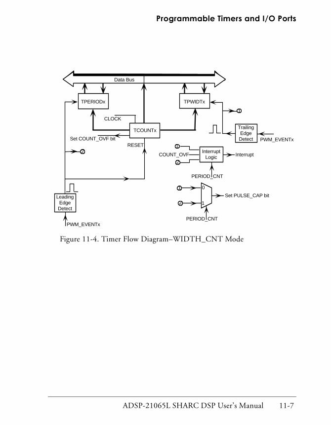
ADSP-21065L SHARC DSP User’s Manual 11-7
Programmable Timers and I/O Ports
Figure 11-4. Timer Flow Diagram–WIDTH_CNT Mode
Data Bus
RESETSet COUNT_OVF bit
TPERIODx TPWIDTx
CLOCK
Interrupt
Set PULSE_CAP bit
PERIOD_CNT
PWM_EVENTx
TCOUNTx
1
1
2
LeadingEdgeDetect
2
COUNT_OVF
PWM_EVENTx222
TrailingEdgeDetect
InterruptLogic
1
2
PERIOD_CNT
0
1

Timer Control Bits and the Interrupt Vectors
11-8 ADSP-21065L SHARC DSP User’s Manual
Timer Control Bits and the Interrupt Vectors
This section describes the timer control bit definitions and the MODE2 register definitions.
TIMENxTimer enable (x=0,1)
0 = Disable
1 = Enable
PWMOUTxPWMOUT/WIDTH_CNT control (x=0,1)
1 = PWM_EVENT is a PWMOUT output.
0 = PWM_EVENT is an WIDTH_CNT input. (default)
PULSE_HIx (x=0,1)Applies to the WIDTH_CNT mode only
0 = 0 to 1 transition is leading edge in the WIDTH_CNT mode.
1 = 1 to 0 transition is leading edge in the WIDTH_CNT mode.
PERIOD_CNTxEnable period count (applicable only to the WIDTH_CNT mode)
0 = Enable width count.
Interrupt and the PULSE_CAPx bits are set when pulse width is captured.
1 = Enable period count.

ADSP-21065L SHARC DSP User’s Manual 11-9
Programmable Timers and I/O Ports
Interrupt and the PULSE_CAPx bits are set when pulse period is captured.
INT_HIxInterrupt vector location. (x=0,1)
The two timers generate interrupts, and these can be latched either at bit 4 (TMZHI) or at bit 23 (TMZLI) of the IRPTL register, as shown in Table 11-1. In addition, these interrupts can be masked using the IMASK register.
Timer Interrupts and the Status StackOnly the timer interrupt on the TMZHI bit pushes the status stack, so, in the above combinations, 00 will not push the status stack, but both 01 and 10 will push the status stack, depending on which timer is programmed to cause the TMZHI interrupt. When using the 11 combination, interrupts generated by either timer push the status stack.
When using the 00 and 11 combinations, the processor latches a logical OR function of the two timer interrupts into the interrupt latch register. The software checks the CNT_EXPx and the EDGE_CAPx bits, deter-mines the source of the interrupt, and takes appropriate action.
Figure 11-5 on page 11-10 shows the mapping of the MODE2 register.
Table 11-1. Timer status
INT_HI1 INT_HI0 Status
0 0 Both timers latch to TMZLI
0 1 timer1 => TMZLI, timer0 => TMZHI
1 0 timer1 => TMZHI, timer0 => TMZLI
1 1 Both timers latch to TMZHI

Timer Control Bits and the Interrupt Vectors
11-10 ADSP-21065L SHARC DSP User’s Manual
Figure 11-5. MODE2 Register
31 30 29 28 27 26 25 24 23 22 21 20 19 18 17 16
1 1 00000 00000000 0
FLG1O0=input1=output
Processor ID
CAFRZ0=cache updates1=cache freeze
Silicon Rev. #
FLG3O
FLG2O
15 14 13 12 11 10 9 8 7 6 5 4 3 2 1 0
0 0 00000 00000000 0
IRQOE0=level-sensitive1=edge-sensitive
PERIOD_CNT00=enable width count1=enable period count
TIMEN00=disable timer1=enable timer
CADIS0=enable cache1=disable cache
INT_HI0Intrpt vector location
BUSLK0=no ext. bus lock1=ext. bus lock
PWMOUT00=WIDTH_CNT input
1=PWMOUT output
PERIOD_CNT1
TIMEN1
PWMOUT1
INT_HI1
PULSE_HI1Leading edge trans.
(WIDTH_CNT mode )0=0-1 transition1=1-0 transition
PULSE_HI0
FLG0O
IRQ1E
IRQ2E
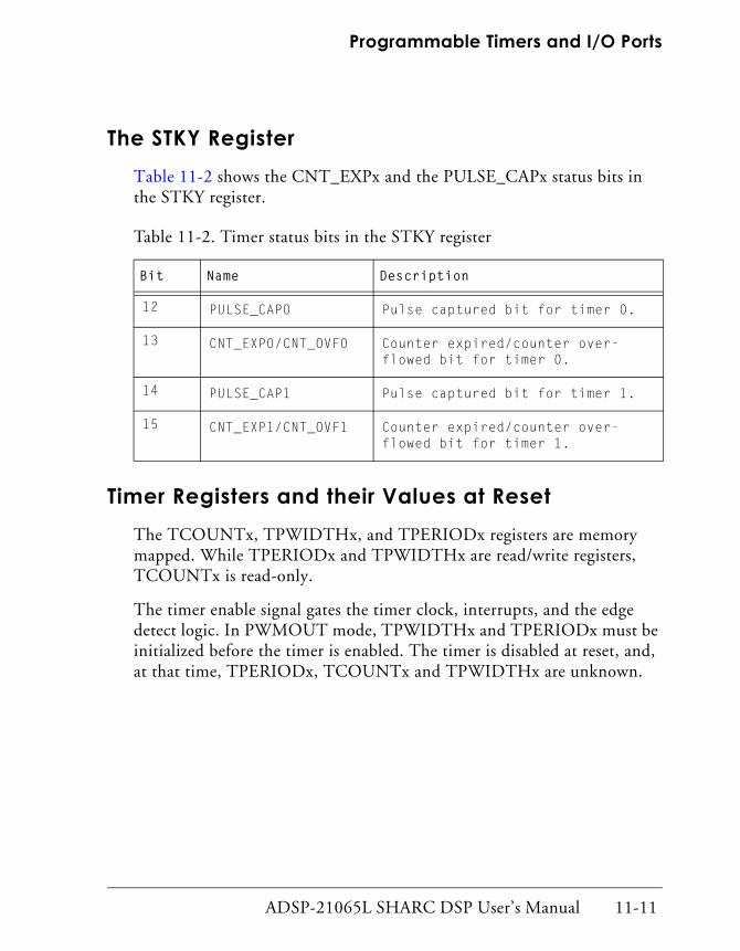
ADSP-21065L SHARC DSP User’s Manual 11-11
Programmable Timers and I/O Ports
The STKY RegisterTable 11-2 shows the CNT_EXPx and the PULSE_CAPx status bits in the STKY register.
Timer Registers and their Values at ResetThe TCOUNTx, TPWIDTHx, and TPERIODx registers are memory mapped. While TPERIODx and TPWIDTHx are read/write registers, TCOUNTx is read-only.
The timer enable signal gates the timer clock, interrupts, and the edge detect logic. In PWMOUT mode, TPWIDTHx and TPERIODx must be initialized before the timer is enabled. The timer is disabled at reset, and, at that time, TPERIODx, TCOUNTx and TPWIDTHx are unknown.
Table 11-2. Timer status bits in the STKY register
Bit Name Description
12 PULSE_CAP0 Pulse captured bit for timer 0.
13 CNT_EXP0/CNT_OVF0 Counter expired/counter over-flowed bit for timer 0.
14 PULSE_CAP1 Pulse captured bit for timer 1.
15 CNT_EXP1/CNT_OVF1 Counter expired/counter over-flowed bit for timer 1.
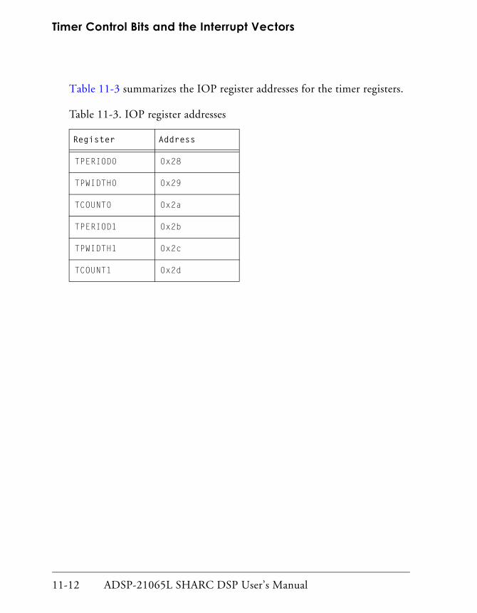
Timer Control Bits and the Interrupt Vectors
11-12 ADSP-21065L SHARC DSP User’s Manual
Table 11-3 summarizes the IOP register addresses for the timer registers.
Table 11-3. IOP register addresses
Register Address
TPERIOD0 0x28
TPWIDTH0 0x29
TCOUNT0 0x2a
TPERIOD1 0x2b
TPWIDTH1 0x2c
TCOUNT1 0x2d

ADSP-21065L SHARC DSP User’s Manual 11-13
Programmable Timers and I/O Ports
Programmable I/O PortsThe processor has twelve flag pins FLAG11-0, which are programmable, general-purpose I/O ports.
The MODE2 register configures the functionality, or direction, of the pins FLAG3-0, and the ASTAT register reflects the value of these flag bits.
The functionality of the FLAG11-4 pins is similar to that of the FLAG3-0, but the IOP registers IOCTL and IOSTAT contain their control and sta-tus bits.
You cannot execute the bitwise operations, such as BIT TST, BIT CLR, and so on, directly on the IOP registers. To perform these operations on the FLAG4-11 pins, you must first transfer the contents of the IOSTAT register (shown in Figure 11-6) to the Register File or to another universal register.
Figure 11-6. IOSTAT register
31 30 29 28 27 26 25 24 23 22 21 20 19 18 17 16
0 0 00000 00000000 0
15 14 13 12 11 10 9 8 7 6 5 4 3 2 1 0
0 0 00000 00000000 0
FLG4
FLG11FLG10FLG9FLG8
FLG7FLG6FLG5
FLGx = FLAGx pin value
Programmable I/O Ports
11-14 ADSP-21065L SHARC DSP User’s Manual
ASTAT is a universal register, so the status on FLAG3-0 can be checked and manipulated using the bitwise operations directly. This is the differ-ence between the FLAG3-0 and the rest of the FLAG pins.
For detailed description of the IOCTL register, where the directions on the I/O ports are set, see Chapter 10, SDRAM Interface.
For a description of the IOSTAT register, see Figure 11-6.
The IOP address locations for the IOCTL and the IOSTAT registers are 0x2e and 0x2f respectively.

ADSP-21065L SHARC DSP User’s Manual 12-1
12 SYSTEM DESIGNFigure 12-0.
Table 12-0.
Listing 12-0.
This chapter provides hardware, software, and system design information to aid users in developing systems built on the ADSP-21065L Digital Sig-nal Processor.
This chapter describes the processor’s pins and shows how to use these sig-nals in your system. This information includes:
• Pin definitions, connections, and states during and after reset.
• Operation of XTAL and CLKIN pins
• Operation of the interrupt and timer pins
• Operation of the FLAG11-0 pins
• Operation of the JTAG interface pins
• Operation of the EZ-ICE Emulator pins
• Input signal conditioning
• High frequency design considerations
• Booting procedures
Figure 12-1 shows example pin connections in a single-processor system. Figure 7-1 on page 7-2 shows example pin connections in a multiproces-sor system.
12-2 ADSP-21065L SHARC DSP User’s Manual
Figure 12-1. Basic single-processor system
%2
%%2
!"#$%&
'"
$!B
,#,
2
$+%
.
.
C
%$B
#2
.#
#.#
#C
$#
9.
9.4
,<
%#
$%#
G
#C,
#$!B2
#B,
#%
&
%#
$%#
G
C,
$!B
$B,
%
3- 5
%
%%
$#
%
%%
3- 5
$#
,#,
$E
%
%%
3- 5$#
%
%
$
!
%
,#
#
1I%
1I.
1I%
1I.
1I%
1I.
1I%1I.
#
"
1%!
;!%42
*%4
+CI,F,0
G2

ADSP-21065L SHARC DSP User’s Manual 12-3
System Design
Pin DefinitionsThis section lists and describes the processor’s pins. Synchronous inputs (S) must meet timing requirements with respect to CLKIN (or to TCK for TMS and TDI). Asynchronous inputs (A) can be asserted asynchronously to CLKIN (or to TCK for TRST).
The following tables list and describe the processor’s pins:
• External port pins Table 12-1 on page 12-4
• Host interface pins Table 12-2 on page 12-7
• SDRAM interface pins Table 12-3 on page 12-10
• Serial port pins Table 12-4 on page 12-11
• System control pins Table 12-5 on page 12-13
• JTAG and emulator pins Table 12-6 on page 12-19
• Miscellaneous pins Table 12-7 on page 12-20
Tie or pull up unused inputs to VDD or GND, except for
• ADDR23-0
• DATA31-0
• FLAG11-0
• SW
• Inputs that have internal pull-up or pull-down resistors (CPA, ACK, DTxX, DRxX, TCLKx, RCLKx, TMS, and TDI)
Leave these pins floating. These pins have a logic-level hold circuit that prevents their input from floating internally.
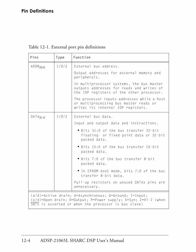
Pin Definitions
12-4 ADSP-21065L SHARC DSP User’s Manual
Table 12-1. External port pin definitions
Pins Type Function
ADDR23-0 I/O/Z External bus address.
Output addresses for external memory and peripherals.
In multiprocessor systems, the bus master outputs addresses for reads and writes of the IOP registers of the other processor.
The processor inputs addresses while a host or multiprocessing bus master reads or writes its internal IOP registers.
DATA31-0 I/O/Z External bus data.
Input and output data and instructions.
• Bits 31:0 of the bus transfer 32-bit floating- or fixed-point data or 32-bit packed data.
• Bits 15:0 of the bus transfer 16-bit packed data.
• Bits 7:0 of the bus transfer 8-bit packed data.
• In EPROM boot mode, bits 7:0 of the bus transfer 8-bit data.
Pull-up resistors on unused DATAx pins are unnecessary.
(a/d)=Active drain; A=Asynchronous; G=Ground; I=Input; (o/d)=Open drain; O=Output; P=Power supply; S=Syn; Z=Hi-Z (when SBTS is asserted or when the processor is bus slave)

ADSP-21065L SHARC DSP User’s Manual 12-5
System Design
DMAG1 O/Z DMA grant 1.
DMA channel 9.
DMAG2 O/Z DMA grant 2.
DMA channel 8.
DMAR1 I/A DMA request1.
DMA channel9.
DMAR2 I/A DMA request 2.
DMA channel 8.
MS3-0 O/Z Memory select lines.
Asserted as chip selects for the corre-sponding banks of external memory. You must define the memory banks in the SYSCON reg-ister.
These lines are decoded memory address lines that change at the same time as the other address lines. These lines remain inactive while no access to external memory occurs. They are active, however, during execution of a conditional memory access instruction, whether or not the condition is true.
In multiprocessing systems, the master pro-cessor outputs the MS3-0 lines.
Table 12-1. External port pin definitions (Cont’d)
Pins Type Function
(a/d)=Active drain; A=Asynchronous; G=Ground; I=Input; (o/d)=Open drain; O=Output; P=Power supply; S=Syn; Z=Hi-Z (when SBTS is asserted or when the processor is bus slave)

Pin Definitions
12-6 ADSP-21065L SHARC DSP User’s Manual
SBTS I/S Suspend bus three-state.
External devices can assert this pin to place the external bus address, data, selects, and strobes—but not the SDRAM con-trol pins—in a high-impedance state for the following cycle.
Any attempt to access external memory while SBTS is asserted stops the processor and suspends the memory access. The processor completes the memory access when SBTS is deasserted.
Use SBTS to recover from deadlock between a host and processor only.
SW I/O/Z Synchronous write select.
Interfaces with synchronous memory devices, including another processor, to provide early indication of an impending write cycle.
The processor asserts this pin when a write cycle is pending. If WR is not asserted later in the write cycle (for example, in a conditional write instruction), the appli-cation can abort the cycle.
In multiprocessing systems, the master pro-cessor outputs SW, and the slave inputs SW to determine if the multiprocessor memory access is a read or write.
Table 12-1. External port pin definitions (Cont’d)
Pins Type Function
(a/d)=Active drain; A=Asynchronous; G=Ground; I=Input; (o/d)=Open drain; O=Output; P=Power supply; S=Syn; Z=Hi-Z (when SBTS is asserted or when the processor is bus slave)
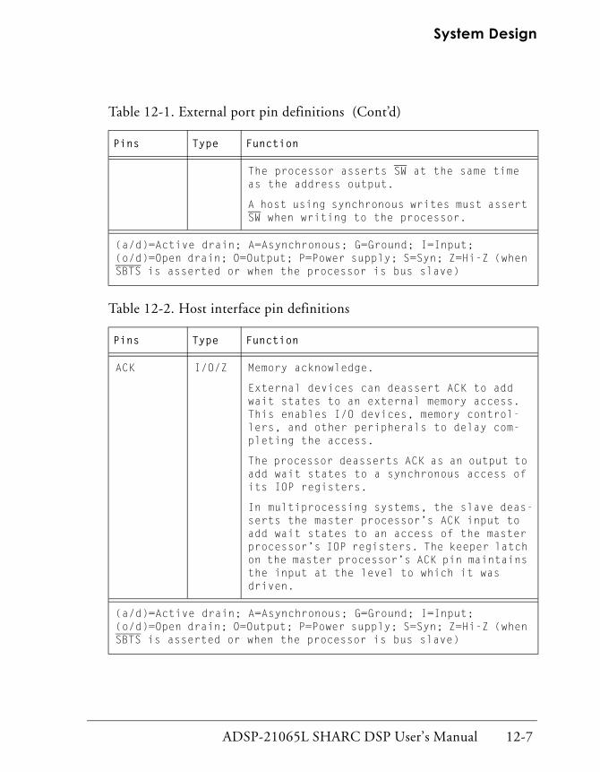
ADSP-21065L SHARC DSP User’s Manual 12-7
System Design
The processor asserts SW at the same time as the address output.
A host using synchronous writes must assert SW when writing to the processor.
Table 12-2. Host interface pin definitions
Pins Type Function
ACK I/O/Z Memory acknowledge.
External devices can deassert ACK to add wait states to an external memory access. This enables I/O devices, memory control-lers, and other peripherals to delay com-pleting the access.
The processor deasserts ACK as an output to add wait states to a synchronous access of its IOP registers.
In multiprocessing systems, the slave deas-serts the master processor’s ACK input to add wait states to an access of the master processor’s IOP registers. The keeper latch on the master processor’s ACK pin maintains the input at the level to which it was driven.
(a/d)=Active drain; A=Asynchronous; G=Ground; I=Input; (o/d)=Open drain; O=Output; P=Power supply; S=Syn; Z=Hi-Z (when SBTS is asserted or when the processor is bus slave)
Table 12-1. External port pin definitions (Cont’d)
Pins Type Function
(a/d)=Active drain; A=Asynchronous; G=Ground; I=Input; (o/d)=Open drain; O=Output; P=Power supply; S=Syn; Z=Hi-Z (when SBTS is asserted or when the processor is bus slave)
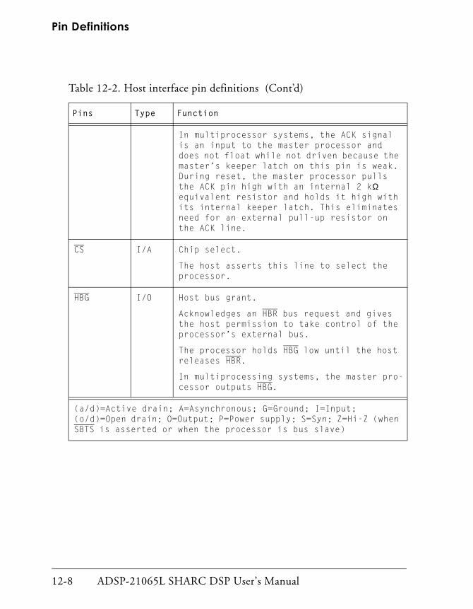
Pin Definitions
12-8 ADSP-21065L SHARC DSP User’s Manual
In multiprocessor systems, the ACK signal is an input to the master processor and does not float while not driven because the master’s keeper latch on this pin is weak. During reset, the master processor pulls the ACK pin high with an internal 2 kΩ equivalent resistor and holds it high with its internal keeper latch. This eliminates need for an external pull-up resistor on the ACK line.
CS I/A Chip select.
The host asserts this line to select the processor.
HBG I/O Host bus grant.
Acknowledges an HBR bus request and gives the host permission to take control of the processor’s external bus.
The processor holds HBG low until the host releases HBR.
In multiprocessing systems, the master pro-cessor outputs HBG.
Table 12-2. Host interface pin definitions (Cont’d)
Pins Type Function
(a/d)=Active drain; A=Asynchronous; G=Ground; I=Input; (o/d)=Open drain; O=Output; P=Power supply; S=Syn; Z=Hi-Z (when SBTS is asserted or when the processor is bus slave)

ADSP-21065L SHARC DSP User’s Manual 12-9
System Design
HBR I/A Host bus request.
The host processor must assert this line to request control of the processor’s external bus.
In multiprocessing systems, the master pro-cessor relinquishes the bus and asserts HBG in response to this request.
To relinquish the bus, the master processor places the address, data, select, and strobe lines in a high-impedance state, but continues to drive the SDRAM control pins.
In multiprocessing systems, HBR has prior-ity over all processor bus requests (BRx).
REDY(o/d) O Host bus acknowledge.
the processor deasserts this line to add wait states to an asynchronous access of its IOP registers made by the host proces-sor.
By default, the output is open drain (o/d). To change output to active drive (a/d), set the ADREDY bit in the SYSCON register.
Table 12-2. Host interface pin definitions (Cont’d)
Pins Type Function
(a/d)=Active drain; A=Asynchronous; G=Ground; I=Input; (o/d)=Open drain; O=Output; P=Power supply; S=Syn; Z=Hi-Z (when SBTS is asserted or when the processor is bus slave)
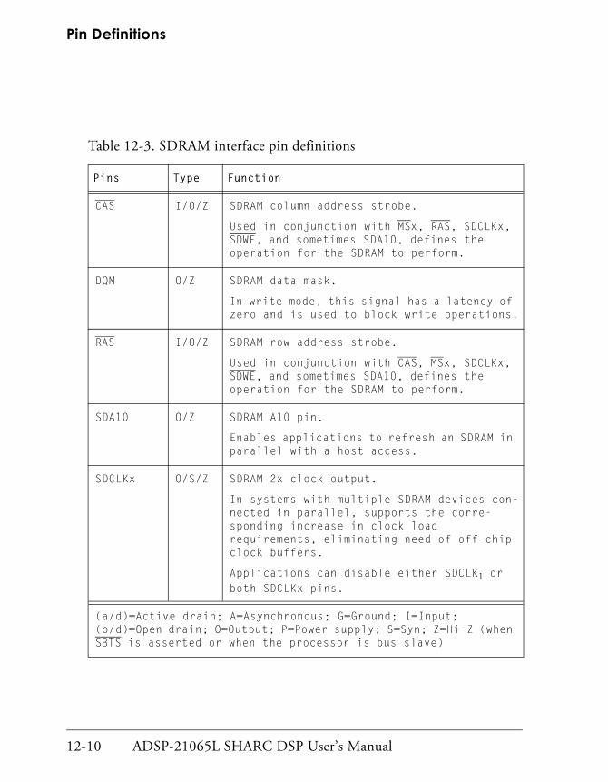
Pin Definitions
12-10 ADSP-21065L SHARC DSP User’s Manual
Table 12-3. SDRAM interface pin definitions
Pins Type Function
CAS I/O/Z SDRAM column address strobe.
Used in conjunction with MSx, RAS, SDCLKx, SDWE, and sometimes SDA10, defines the operation for the SDRAM to perform.
DQM O/Z SDRAM data mask.
In write mode, this signal has a latency of zero and is used to block write operations.
RAS I/O/Z SDRAM row address strobe.
Used in conjunction with CAS, MSx, SDCLKx, SDWE, and sometimes SDA10, defines the operation for the SDRAM to perform.
SDA10 O/Z SDRAM A10 pin.
Enables applications to refresh an SDRAM in parallel with a host access.
SDCLKx O/S/Z SDRAM 2x clock output.
In systems with multiple SDRAM devices con-nected in parallel, supports the corre-sponding increase in clock load requirements, eliminating need of off-chip clock buffers.
Applications can disable either SDCLK1 or both SDCLKx pins.
(a/d)=Active drain; A=Asynchronous; G=Ground; I=Input; (o/d)=Open drain; O=Output; P=Power supply; S=Syn; Z=Hi-Z (when SBTS is asserted or when the processor is bus slave)

ADSP-21065L SHARC DSP User’s Manual 12-11
System Design
SDCKE I/O/Z SDRAM clock enable.
Enables and disables the CLK signal.
Used to enter self-refresh.
SDWE I/O/Z SDRAM write enable.
Used in conjunction with CAS, MSx, RAS, SDCLKx, and sometimes SDA10, defines the operation for the SDRAM to perform.
Table 12-4. Serial port pin definitions
Pins Type Function
DRx_X I Data receive.
SPORTs 0/1, channels A /B.
Each DRxX pin has a 50 kΩ internal pull-up resistor.
DTx_X O Data transmit.
SPORTs 0/1, channels A /B.
Each DTxX pin has a 50 kΩ internal pull-up resistor.
(a/d)=Active drain; A=Asynchronous; G=Ground; I=Input; (o/d)=Open drain; O=Output; P=Power supply; S=Syn; Z=Hi-Z (when SBTS is asserted or when the processor is bus slave)
Table 12-3. SDRAM interface pin definitions (Cont’d)
Pins Type Function
(a/d)=Active drain; A=Asynchronous; G=Ground; I=Input; (o/d)=Open drain; O=Output; P=Power supply; S=Syn; Z=Hi-Z (when SBTS is asserted or when the processor is bus slave)

Pin Definitions
12-12 ADSP-21065L SHARC DSP User’s Manual
RCLKx I/O Receive clock for SPORTs 0 and 1.
Each RCLK pin has a 50 kΩ internal pull-up resistor.
RFSx I/O Receive frame sync for SPORTs 0 and 1.
TCLKx I/O Transmit clock for SPORTs 0 and 1.
Each TCLK pin has a 50 kΩ internal pull-up resistor.
TFSx I/O Transmit frame sync for SPORTs 0 and 1.
Table 12-4. Serial port pin definitions (Cont’d)
Pins Type Function
(a/d)=Active drain; A=Asynchronous; G=Ground; I=Input; (o/d)=Open drain; O=Output; P=Power supply; S=Syn; Z=Hi-Z (when SBTS is asserted or when the processor is bus slave)

ADSP-21065L SHARC DSP User’s Manual 12-13
System Design
Table 12-5. System control pin definitions
Pins Type Function
BMS I/O/Z Boot memory select.
This is a system configuration selection that you need to hard wire.
• Output
Used as chip select for boot EPROM devices when BSEL=1.
In multiprocessor systems, the master processor outputs BMS.
• Input
When asserted, indicates no booting will occur.
The processor will begin executing instructions from external memory.
When an output, this pin is three-statable in EPROM boot mode only. For details, see “Booting” on page 12-49.
BMSTR O Bus master output.
Used in multiprocessor systems only.
Indicates whether the processor is current bus master of the shared external bus.
The processor asserts this pin high only while it is bus master. Do not connect to BMSTR on another ADSP-21065L.
(a/d)=Active drain; A=Asynchronous; G=Ground; I=Input; (o/d)=Open drain; O=Output; P=Power supply; S=Syn; Z=Hi-Z (when SBTS is asserted or when the processor is bus slave)
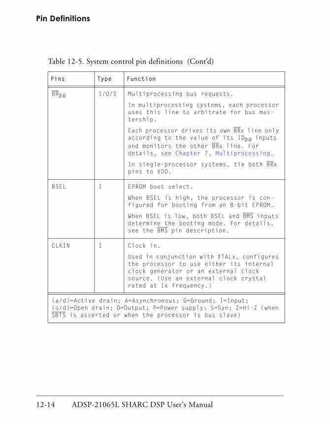
Pin Definitions
12-14 ADSP-21065L SHARC DSP User’s Manual
BR2-0 I/O/S Multiprocessing bus requests.
In multiprocessing systems, each processor uses this line to arbitrate for bus mas-tership.
Each processor drives its own BRx line only according to the value of its ID2-0 inputs and monitors the other BRx line. For details, see Chapter 7‚ Multiprocessing.
In single-processor systems, tie both BRx pins to VDD.
BSEL I EPROM boot select.
When BSEL is high, the processor is con-figured for booting from an 8-bit EPROM.
When BSEL is low, both BSEL and BMS inputs determine the booting mode. For details, see the BMS pin description.
CLKIN I Clock in.
Used in conjunction with XTALx, configures the processor to use either its internal clock generator or an external clock source. (Use an external clock crystal rated at 1x frequency.)
Table 12-5. System control pin definitions (Cont’d)
Pins Type Function
(a/d)=Active drain; A=Asynchronous; G=Ground; I=Input; (o/d)=Open drain; O=Output; P=Power supply; S=Syn; Z=Hi-Z (when SBTS is asserted or when the processor is bus slave)

ADSP-21065L SHARC DSP User’s Manual 12-15
System Design
CLKIN (Cont’d)
I • Internal clock generator
Connecting the necessary components to CLKIN and XTALx enables the internal clock generator.
The processor’s internal clock generator multiplies the 1x clock to generate 2x clock for its core and SDRAM interface.
• The processor drives 2x clock out on the SDCLKx pins for the SDRAM interface to use.
• External clock source
Connecting the 1x external clock to CLKIN while leaving XTALx unconnected configures the processor to use the external clock source.
The instruction cycle rate is equal to 2x CLKIN.
You cannot halt, change, or operate CLKIN below the specified frequency.
Table 12-5. System control pin definitions (Cont’d)
Pins Type Function
(a/d)=Active drain; A=Asynchronous; G=Ground; I=Input; (o/d)=Open drain; O=Output; P=Power supply; S=Syn; Z=Hi-Z (when SBTS is asserted or when the processor is bus slave)
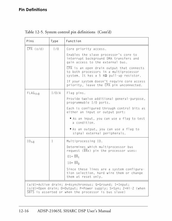
Pin Definitions
12-16 ADSP-21065L SHARC DSP User’s Manual
CPA (o/d) I/O Core priority access.
Enables the slave processor’s core to interrupt background DMA transfers and gain access to the external bus.
CPA is an open drain output that connects to both processors in a multiprocessor system. It has a 5 KΩ pull-up resistor.
If your system doesn’t require core access priority, leave the CPA pin unconnected.
FLAG11-0 I/O/A Flag pins.
Provide twelve additional general-purpose, programmable I/O ports.
Each is configured through control bits as either an input or output port:
• As an input, you can use a flag to test a condition.
• As an output, you can use a flag to signal external peripherals.
ID1-0 I Multiprocessing ID.
Determines which multiprocessor bus request (BRx) pin the processor uses:
01= BR1
10= BR2
Since these lines are a system configura-tion selection, hard wire them or change them at reset only.
Table 12-5. System control pin definitions (Cont’d)
Pins Type Function
(a/d)=Active drain; A=Asynchronous; G=Ground; I=Input; (o/d)=Open drain; O=Output; P=Power supply; S=Syn; Z=Hi-Z (when SBTS is asserted or when the processor is bus slave)

ADSP-21065L SHARC DSP User’s Manual 12-17
System Design
IRQ2-0 I/A Interrupt request lines.
Either edge-triggered or level-sensitive.
PWM_EVENT1-0 I/O/A PWM output/event capture.
IN PMWOUT mode, this pin is an output that functions as a timer counter.
In WIDTH_CNT mode, this pin is an input that functions as a pulse counter/event capture.
RD I/O/Z Memory read strobe.
Asserted when the processor reads from external memory devices or from the other processor in a multiprocessor system.
External devices, including another pro-cessor, must assert RD to read from the processor’s IOP register.
In multiprocessing systems, the master processor outputs RD, and the slave inputs RD.
Except during a host transition cycle (HTC), do not deassert the RD strobe (low-to-high transition) while ACK or REDY are deasserted. Doing so causes the pro-cessor to hang.
Operation of the RD signal changes when a host asserts CS. For details, see “Host Transfers” on page 8-11.
Table 12-5. System control pin definitions (Cont’d)
Pins Type Function
(a/d)=Active drain; A=Asynchronous; G=Ground; I=Input; (o/d)=Open drain; O=Output; P=Power supply; S=Syn; Z=Hi-Z (when SBTS is asserted or when the processor is bus slave)
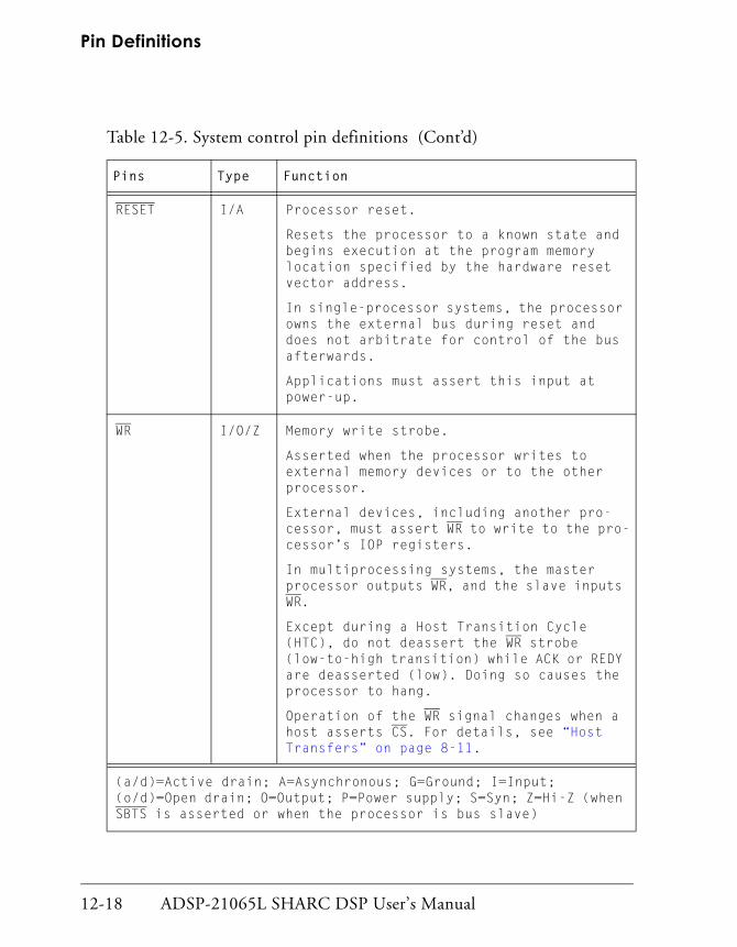
Pin Definitions
12-18 ADSP-21065L SHARC DSP User’s Manual
RESET I/A Processor reset.
Resets the processor to a known state and begins execution at the program memory location specified by the hardware reset vector address.
In single-processor systems, the processor owns the external bus during reset and does not arbitrate for control of the bus afterwards.
Applications must assert this input at power-up.
WR I/O/Z Memory write strobe.
Asserted when the processor writes to external memory devices or to the other processor.
External devices, including another pro-cessor, must assert WR to write to the pro-cessor’s IOP registers.
In multiprocessing systems, the master processor outputs WR, and the slave inputs WR.
Except during a Host Transition Cycle (HTC), do not deassert the WR strobe (low-to-high transition) while ACK or REDY are deasserted (low). Doing so causes the processor to hang.
Operation of the WR signal changes when a host asserts CS. For details, see “Host Transfers” on page 8-11.
Table 12-5. System control pin definitions (Cont’d)
Pins Type Function
(a/d)=Active drain; A=Asynchronous; G=Ground; I=Input; (o/d)=Open drain; O=Output; P=Power supply; S=Syn; Z=Hi-Z (when SBTS is asserted or when the processor is bus slave)

ADSP-21065L SHARC DSP User’s Manual 12-19
System Design
XTAL O Crystal oscillator terminal.
Used in conjunction with CLKIN to enable the processors internal clock generator or to disable it to use an external clock source.
Table 12-6. JTAG and emulator pin definitions
Pins Type Function
EMU (O/D) O Emulation status.
Connect to the ADSP-21065L EZ-ICE target only.
TCK I Test clock (JTAG).
Provides an asynchronous clock for the JTAG boundary scan.
TDI I/S Test data input (JTAG).
Serial data input to the boundary scan path.
This pin has an internal 20 kΩ pull-up resistor.
(a/d)=Active drain; A=Asynchronous; G=Ground; I=Input; (o/d)=Open drain; O=Output; P=Power supply; S=Syn; Z=Hi-Z (when SBTS is asserted or when the processor is bus slave)
Table 12-5. System control pin definitions (Cont’d)
Pins Type Function
(a/d)=Active drain; A=Asynchronous; G=Ground; I=Input; (o/d)=Open drain; O=Output; P=Power supply; S=Syn; Z=Hi-Z (when SBTS is asserted or when the processor is bus slave)

Pin Definitions
12-20 ADSP-21065L SHARC DSP User’s Manual
TDO O Test data output (JTAG).
Serial scan output from the boundary scan path.
TMS I/S Test mode select (JTAG).
Controls the test state machine.
This pin has an internal 20 kΩ pull-up resistor.
TRST I/A Test reset (JTAG).
Resets the test state machine.
After power-up, applications must assert (pulse) or hold this pin low. Do not leave this pin unconnected.
This pin has an internal 20 kΩ pull-up resistor.
Table 12-7. Miscellaneous pin definitions
Pins Type Function
GND G Power supply return
NC — Do not connect
VDD P Power supply
(a/d)=Active drain; A=Asynchronous; G=Ground; I=Input; (o/d)=Open drain; O=Output; P=Power supply; S=Syn; Z=Hi-Z (when SBTS is asserted or when the processor is bus slave)
Table 12-6. JTAG and emulator pin definitions (Cont’d)
Pins Type Function
(a/d)=Active drain; A=Asynchronous; G=Ground; I=Input; (o/d)=Open drain; O=Output; P=Power supply; S=Syn; Z=Hi-Z (when SBTS is asserted or when the processor is bus slave)

ADSP-21065L SHARC DSP User’s Manual 12-21
System Design
Figure 12-2 shows how the processor transfers different data word sizes over the external port.
Figure 12-2. External port alignment
32-bit Float or FixedD31-D0
32-bit Packed
16-bit Packed
8-bit Packed
EPROMBoot
31 24 16 8 0
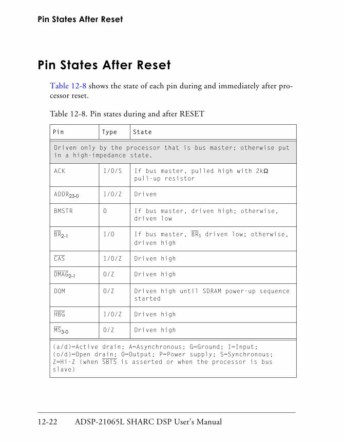
Pin States After Reset
12-22 ADSP-21065L SHARC DSP User’s Manual
Pin States After ResetTable 12-8 shows the state of each pin during and immediately after pro-cessor reset.
Table 12-8. Pin states during and after RESET
Pin Type State
Driven only by the processor that is bus master; otherwise put in a high-impedance state.
ACK I/O/S If bus master, pulled high with 2kΩ pull-up resistor
ADDR23-0 I/O/Z Driven
BMSTR O If bus master, driven high; otherwise, driven low
BR2-1 I/O If bus master, BR1 driven low; otherwise, driven high
CAS I/O/Z Driven high
DMAG2-1 O/Z Driven high
DQM O/Z Driven high until SDRAM power-up sequence started
HBG I/O/Z Driven high
MS3-0 O/Z Driven high
(a/d)=Active drain; A=Asynchronous; G=Ground; I=Input; (o/d)=Open drain; O=Output; P=Power supply; S=Synchronous; Z=Hi-Z (when SBTS is asserted or when the processor is bus slave)

ADSP-21065L SHARC DSP User’s Manual 12-23
System Design
RAS I/O/Z Driven high
RD I/O/Z Driven high
SDA10 O/Z Driven
SDCKE I/O/Z Driven high
SDCLKx O/S/Z Driven
SDWE I/O/Z Driven high
SW I/O/Z Driven high
WR I/O/Z Driven high
Independent of bus master
BMS I/O/Z Input if BSEL =0;output if BSEL=1
BSEL I Input
CLKIN I Input
CPA (o/d) I/O/Z Hi-Z
CS I Input
DATA31-0 I/O/Z Hi-Z
DMAR2-1 I Inputs
Table 12-8. Pin states during and after RESET (Cont’d)
Pin Type State
(a/d)=Active drain; A=Asynchronous; G=Ground; I=Input; (o/d)=Open drain; O=Output; P=Power supply; S=Synchronous; Z=Hi-Z (when SBTS is asserted or when the processor is bus slave)

Pin States After Reset
12-24 ADSP-21065L SHARC DSP User’s Manual
FLAG11-0 I/O/A Inputs
HBR I/A Inputs
ID1-0 I Inputs
IRQ2-0 I/A Inputs
PWM_EVENT1-0 I/O/A Inputs at RESET
REDY (o/d) O/Z Hi-Z
RESET I/A Input
SBTS I/S Input; Puts the master processor in high-impedance state during reset.
XTAL O Output
Serial Ports
DRx_X I Input
DTx_X O Hi-Z (for multichannel)
RCLKx I/O Hi-Z
TCLKx I/O Hi-Z
RFSx I/O Hi-Z
TFSx I/O Hi-Z
Table 12-8. Pin states during and after RESET (Cont’d)
Pin Type State
(a/d)=Active drain; A=Asynchronous; G=Ground; I=Input; (o/d)=Open drain; O=Output; P=Power supply; S=Synchronous; Z=Hi-Z (when SBTS is asserted or when the processor is bus slave)
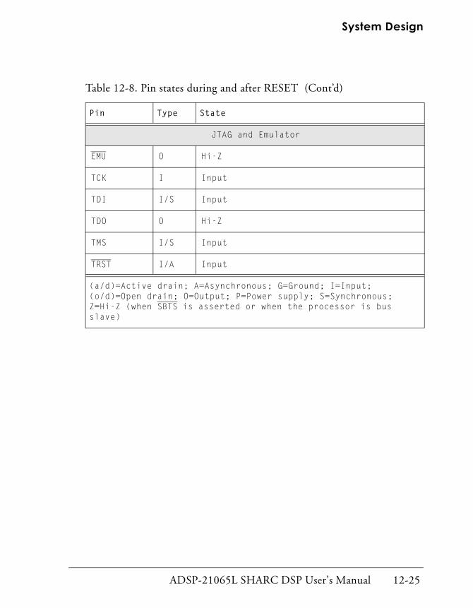
ADSP-21065L SHARC DSP User’s Manual 12-25
System Design
JTAG and Emulator
EMU O Hi-Z
TCK I Input
TDI I/S Input
TDO O Hi-Z
TMS I/S Input
TRST I/A Input
Table 12-8. Pin states during and after RESET (Cont’d)
Pin Type State
(a/d)=Active drain; A=Asynchronous; G=Ground; I=Input; (o/d)=Open drain; O=Output; P=Power supply; S=Synchronous; Z=Hi-Z (when SBTS is asserted or when the processor is bus slave)
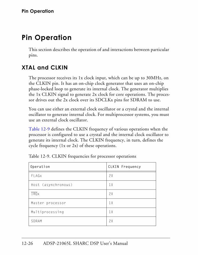
Pin Operation
12-26 ADSP-21065L SHARC DSP User’s Manual
Pin OperationThis section describes the operation of and interactions between particular pins.
XTAL and CLKINThe processor receives its 1x clock input, which can be up to 30MHz, on the CLKIN pin. It has an on-chip clock generator that uses an on-chip phase-locked loop to generate its internal clock. The generator multiplies the 1x CLKIN signal to generate 2x clock for core operations. The proces-sor drives out the 2x clock over its SDCLKx pins for SDRAM to use.
You can use either an external clock oscillator or a crystal and the internal oscillator to generate internal clock. For multiprocessor systems, you must use an external clock oscillator.
Table 12-9 defines the CLKIN frequency of various operations when the processor is configured to use a crystal and the internal clock oscillator to generate its internal clock. The CLKIN frequency, in turn, defines the cycle frequency (1x or 2x) of these operations.
Table 12-9. CLKIN frequencies for processor operations
Operation CLKIN Frequency
FLAGx 2X
Host (asynchronous) 1X
IRQx 2X
Master processor 1X
Multiprocessing 1X
SDRAM 2X

ADSP-21065L SHARC DSP User’s Manual 12-27
System Design
To enable the on-chip generator, connect CLKIN and XTAL to the neces-sary external components (for details, see the processor’s data sheet). To use 1x clock, connect CLKIN to an external clock oscillator, and leave XTAL unconnected.
Because the on-chip generator’s phase-locked loop requires some time to achieve phase lock, CLKIN must be valid for a minimum time period dur-ing reset before the application deasserts the RESET signal. For details, see the processor’s data sheet.
Input Synchronization DelayThe processor has several asynchronous inputs—RESET, TRST, HBR, CS, DMAR2-1, and IRQ2-0, and, when configured as inputs, PWM_EVENTx and FLAG11-0. Applications can assert these inputs in arbitrary phase to the processor clock, CLKIN. The processor synchro-nizes the inputs before it recognizes them. The delay associated with recognition is called synchronization delay.
For the processor to recognize any asynchronous input in a particular cycle, the input must be valid before the recognition phase. If an input does not meet the setup time on a given cycle, the processor may recognize it in the current cycle or during the next cycle (see Table 12-9 for cycle definitions).
So, to ensure recognition of an asynchronous input, make sure your appli-cation asserts the input for at least one full processor cycle in addition to
Serial ports 1X
Wait states (external memory) 1X
Table 12-9. CLKIN frequencies for processor operations (Cont’d)
Operation CLKIN Frequency

Pin Operation
12-28 ADSP-21065L SHARC DSP User’s Manual
the setup and hold time, except for RESET, which you must assert for at least four processor cycles. For details, see the processor’s data sheet.
External Interrupt and Timer PinsYou can use the processor’s external interrupt (IRQx) pins, FLAGx pins, and PWM_EVENT pins to send and receive control signals to and from other devices in the system.
The IRQ2-0 pins receive hardware interrupt signals. Devices that require the processor to perform some task on demand can generate interrupts. A memory-mapped peripheral, for example, can generate an interrupt to alert the processor that it has data available. For details, see Chapter 3‚ Program Sequencing.
The PWM_EVENT1-0 timer pins are programmable and function inde-pendently in either pulse width generation mode or in pulse count and capture mode. In pulse width generation mode, the timer pins output a modulated waveform with an arbitrary pulse width, and in pulse count and capture mode, they measure the high or low pulse width or period of an input waveform.
Both modes generate timer INT_HIx interrupts, which indicate to other devices that the programmed time period has expired. For details see, Chapter 11‚ Programmable Timers and I/O Ports.
Flag PinsThe FLAG11-0 pins enable single-bit signaling between the processor and other devices. For example, the processor can raise an output flag to inter-rupt a host
Each flag pin is programmable as either an input or output port. You can condition many processor instructions on a flag’s input value to facilitate

ADSP-21065L SHARC DSP User’s Manual 12-29
System Design
efficient communication and synchronization between dual processors or with other interfaces.
All flag pins are bidirectional and have the same functionality. But the control and status bits for FLAG3-0 and FLAG11-4 are located in different registers.
The control and status bits for FLAG3-0 are in the MODE2 register and ASTAT register, respectively. Because both of these registers are universal registers, you can execute the bit wise operations, BIT, BIT TST, CLR, and so on, directly on them.
To program the direction of the FLAG3-0 pins, set or clear the control bits in the MODE2 register, as shown in Table 12-10.
Table 12-10. MODE2 control bits for the FLAG3-0 pins
Bit Name Description
15 FLG0O FLG0O direction select.
0 = input
1 = output
16 FLG1O FLG1O direction select.
0 = input
1 = output
17 FLG2O FLG2O direction select.
0 = input
1 = output
18 FLG3O FLG3O direction select.
0 = input
1 = output
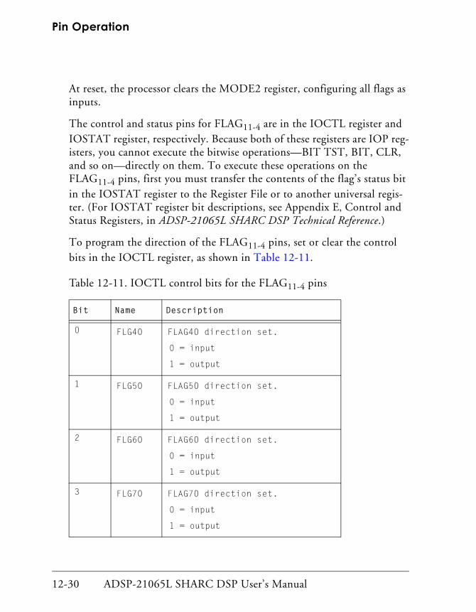
Pin Operation
12-30 ADSP-21065L SHARC DSP User’s Manual
At reset, the processor clears the MODE2 register, configuring all flags as inputs.
The control and status pins for FLAG11-4 are in the IOCTL register and IOSTAT register, respectively. Because both of these registers are IOP reg-isters, you cannot execute the bitwise operations—BIT TST, BIT, CLR, and so on—directly on them. To execute these operations on the FLAG11-4 pins, first you must transfer the contents of the flag’s status bit in the IOSTAT register to the Register File or to another universal regis-ter. (For IOSTAT register bit descriptions, see Appendix E‚ Control and Status Registers, in ADSP-21065L SHARC DSP Technical Reference.)
To program the direction of the FLAG11-4 pins, set or clear the control bits in the IOCTL register, as shown in Table 12-11.
Table 12-11. IOCTL control bits for the FLAG11-4 pins
Bit Name Description
0 FLG4O FLAG4O direction set.
0 = input
1 = output
1 FLG5O FLAG5O direction set.
0 = input
1 = output
2 FLG6O FLAG6O direction set.
0 = input
1 = output
3 FLG7O FLAG7O direction set.
0 = input
1 = output

ADSP-21065L SHARC DSP User’s Manual 12-31
System Design
At reset, the processor clears the IOCTL register, configuring all flags as inputs.
Flag Inputs
When a flag is programmed as an input, the processor stores its value in a bit in either the ASTAT register or the IOSTAT register, depending on the particular flag (FLAG3-0 or FLAG11-4).
Each cycle, the processor updates the flag’s status bit with the input value of its pin. Since flag inputs can be asynchronous to the processor clock, if the rising edge of the input misses the setup requirement for the cycle, a
4 FLG8O FLAG8O direction set.
0 = input
1 = output
5 FLG9O FLAG9O direction set.
0 = input
1 = output
6 FLG10O FLAG10O direction set.
0 = input
1 = output
7 FLG11O FLAG11O direction set.
0 = input
1 = output
Table 12-11. IOCTL control bits for the FLAG11-4 pins (Cont’d)
Bit Name Description

Pin Operation
12-32 ADSP-21065L SHARC DSP User’s Manual
one-cycle delay occurs before a change on the pin appears in either ASTAT or IOSTAT, as shown in Table 12-12.
When a flag pin is configured as an input, its status bit in ASTAT or IOSTAT is read-only. Otherwise, you can read and write the status bit. You can specify the bit states of the ASTAT and IOSTAT flags as condi-tions in conditional instructions. For details, see “Flag Pins” on page 12-28.
Table 12-12. FLAGxO status bits
Register Bit Name Description
ASTAT 19 FLG0O FLAG0 value
20 FLG1O FLAG1 value
21 FLG2O FLAG2 value
22 FLG3O FLAG3 value
IOSTAT 0 FLG4O FLAG4 value
1 FLG5O FLAG5 value
2 FLG6O FLAG6 value
3 FLG7O FLAG7 value
4 FLG8O FLAG8 value
5 FLG9O FLAG9 value
6 FLG10O FLAG10 value
7 FLG11O FLAG11 value
ADSP-21065L SHARC DSP User’s Manual 12-33
System Design
Flag Outputs
When a flag is configured as an output, the state of the pin corresponds to the value of the flag’s status bit in either the ASTAT or the IOSTAT register.
Your application can set or clear the ASTAT or IOSTAT flag bits to pro-vide a signal to the other processor or to a peripheral. Figure 12-3 on page 12-34 shows the timing of a flag output.
When an interrupt service routine pushes ASTAT or IOSTAT onto the status stack, the flag bits in ASTAT and IOSTAT are not affected.
The values of these bits carry over from the main program to the service routine and from the service routine back to the main program (in a pop of the status stack). For details, see “Status Stack Save and Restore” on page 3-48.
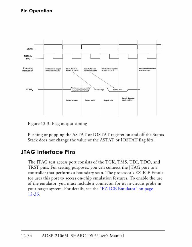
Pin Operation
12-34 ADSP-21065L SHARC DSP User’s Manual
Figure 12-3. Flag output timing
Pushing or popping the ASTAT or IOSTAT register on and off the Status Stack does not change the value of the ASTAT or IOSTAT flag bits.
JTAG Interface PinsThe JTAG test access port consists of the TCK, TMS, TDI, TDO, and TRST pins. For testing purposes, you can connect the JTAG port to a controller that performs a boundary scan. The processor’s EZ-ICE Emula-tor uses this port to access on-chip emulation features. To enable the use of the emulator, you must include a connector for its in-circuit probe in your target system. For details, see the “EZ-ICE Emulator” on page 12-36.
! "#"
$%& '%
(
'%
! #"
$%& '% (
'%
'"
! #"
! ) ! *
%"#" ( %"#" + %"#" +
%"#" (,
#" (

ADSP-21065L SHARC DSP User’s Manual 12-35
System Design
For proper processor operation, your application must assert (pulse or hold low) the JTAG TRST input after power-up. Otherwise, the JTAG port enters an undefined state, which can cause the processor to drive out on the I/O pins rather than put them in a high-impedance state at reset as normal.
You can use a jumper to ground on the EZ-ICE target board connector to hold TRST low. (See Figure 12-4 on page 12-38.)
Do not leave this pin unconnected!

EZ-ICE Emulator
12-36 ADSP-21065L SHARC DSP User’s Manual
EZ-ICE EmulatorThe processor’s EZ-ICE Emulator is a development tool for debugging programs running in real time on your ADSP-21065L target system hardware.
By connecting directly to the target processor through its JTAG interface, the EZ-ICE Emulator provides a controlled environment for observing, debugging, and testing activities in a target system.
The EZ-ICE emulator can monitor system behavior while running at full speed. It enables you to examine and alter memory locations and processor registers and stacks.
Controlling the target system’s processor through the processor’s IEEE 1149.1 JTAG Test Access Port, the EZ-ICE ensures non-intrusive in-cir-cuit emulation. The EZ-ICE emulator does not impact target loading or timing, and its in-circuit probe connects to an IBM PC host computer equipped with an ISA bus plug-in board.
Target systems must have a 14-pin, male connector that accepts the EZ-ICE emulator’s in-circuit probe, a 14-pin, female plug.
Target Board Connector for EZ-ICE ProbeThe EZ-ICE Emulator uses the processor’s IEEE 1149.1 JTAG test access port to monitor and control the target board processor during emulation.
The EZ-ICE probe uses a 14-pin connector (a pin strip header) such as that shown in Figure 12-4 on page 12-38 to provide the target system access to the processor’s CLKIN, TMS, TCK, TRST, TDI, TDO, EMU, and GND signals. The EZ-ICE probe plugs directly into this connector for chip-on-board emulation.
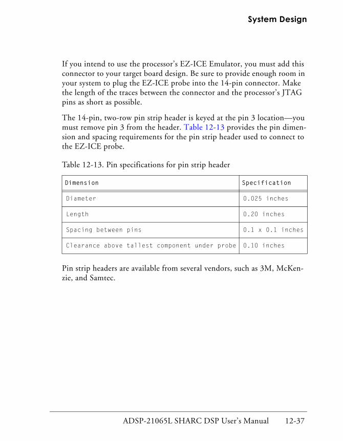
ADSP-21065L SHARC DSP User’s Manual 12-37
System Design
If you intend to use the processor’s EZ-ICE Emulator, you must add this connector to your target board design. Be sure to provide enough room in your system to plug the EZ-ICE probe into the 14-pin connector. Make the length of the traces between the connector and the processor’s JTAG pins as short as possible.
The 14-pin, two-row pin strip header is keyed at the pin 3 location—you must remove pin 3 from the header. Table 12-13 provides the pin dimen-sion and spacing requirements for the pin strip header used to connect to the EZ-ICE probe.
Pin strip headers are available from several vendors, such as 3M, McKen-zie, and Samtec.
Table 12-13. Pin specifications for pin strip header
Dimension Specification
Diameter 0.025 inches
Length 0.20 inches
Spacing between pins 0.1 x 0.1 inches
Clearance above tallest component under probe 0.10 inches
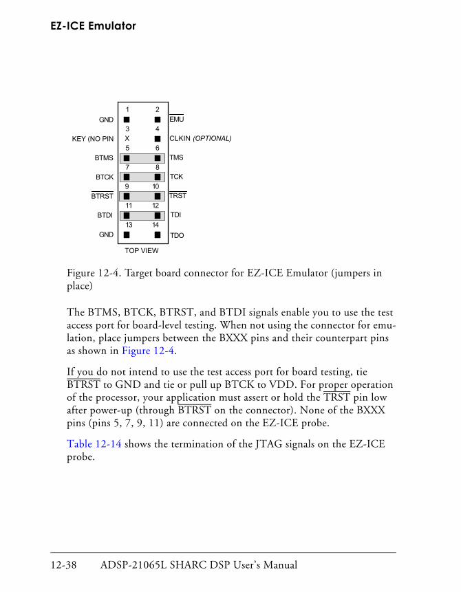
EZ-ICE Emulator
12-38 ADSP-21065L SHARC DSP User’s Manual
Figure 12-4. Target board connector for EZ-ICE Emulator (jumpers in place)
The BTMS, BTCK, BTRST, and BTDI signals enable you to use the test access port for board-level testing. When not using the connector for emu-lation, place jumpers between the BXXX pins and their counterpart pins as shown in Figure 12-4.
If you do not intend to use the test access port for board testing, tie BTRST to GND and tie or pull up BTCK to VDD. For proper operation of the processor, your application must assert or hold the TRST pin low after power-up (through BTRST on the connector). None of the BXXX pins (pins 5, 7, 9, 11) are connected on the EZ-ICE probe.
Table 12-14 shows the termination of the JTAG signals on the EZ-ICE probe.

ADSP-21065L SHARC DSP User’s Manual 12-39
System Design
Figure 12-5 on page 12-40 shows JTAG scan path connections for systems that contain two processors.
Table 12-14. Termination of EZ-ICE signals
Signal Termination
TMS Driven through 22Ω resistor (16 mA driver)
TCK Driven at 10 MHz through 22Ω resistor (16 mA driver)
TRST Driven through 22Ω resistor (16 mA driver) (pulled up by an on-chip 20kΩ resistor)
Driven low until the EZ-ICE software turns on the EZ-ICE probe. After software start-up, TRST is driven high.
TDI Driven through 22Ω resistor (16 mA driver)
TDO One TTL load, split termination (160/220)
CLKIN One TTL load, split termination (160/220)
EMU Active low. 4.7 kΩ pull-up resistor, one TTL load (open drain output from the processor)

EZ-ICE Emulator
12-40 ADSP-21065L SHARC DSP User’s Manual
Figure 12-5. JTAG scan path connections for multiprocessor systems
Connecting CLKIN to pin 4 of the EZ-ICE header is optional. The emu-lator uses CLKIN only when performing synchronous multiprocessor operations, such as starting, stopping, and single-stepping two processors. If you do not need these operations to execute synchronously on both pro-cessors, tie pin 4 on the EZ-ICE header to ground.
If you need to execute synchronous multiprocessor operations, and CLKIN is connected, clock skew between both processors and the CLKIN pin on the EZ-ICE header must be minimal. A clock skew that is too large can hold off synchronous operations between processors by one cycle. Since, in this configuration, TCK, TMS, CLKIN (optional), and EMU are critical signals in terms of clock skew, make sure to lay them out as short as possible on your board.
If you do not need to execute synchronous multiprocessor operations, and CLKIN is not connected, use appropriate parallel termination on TCK and TMS. In this configuration, TDI, TDO, and TRST are not critical signals in terms of clock skew.
!"
#$
%&%
'
('
'!!'
!"
%)
%)
%)
ADSP-21065L SHARC DSP User’s Manual 12-41
System Design
Input Signal ConditioningThe processor is a CMOS device. It has input conditioning circuits that filter or latch input signals to reduce susceptibility to reflections. This sec-tion describes why these circuits are necessary and how they affect input signals.
A typical CMOS input consists of an inverter with specific N and P device sizes that cause a switching point of approximately 1.4V. This level is the selected midpoint of the standard TTL interface specification of VIL=0.8V and VIH=2.0V.
Because the input inverter has a fast response to input signals and external glitches wider than approximately 1 ns, filter circuits and hysteresis are added after the input inverter on some processor inputs.
Hysteresis is used only on the RESET input signal. Hysteresis raises the switching point of the input inverter to slightly above 1.4V for a rising edge and lowers it to slightly below 1.4V for a falling edge. The value of the hysteresis is approximately ± 0.1V.
Hysteresis is intended to prevent the multiple triggering of signals, which are allowed to rise slowly, as might be expected on a reset line with a delay implemented by an RC input circuit. Hysteresis is not intended to reduce the affect of ringing on input signals with fast edges since the amount of hysteresis allowed on a CMOS chip is too small to make much difference. The tolerance of the VIL and VIH TTL input levels under worst case con-ditions limits the amount of hysteresis. For exact specifications, see the processor’s data sheet.
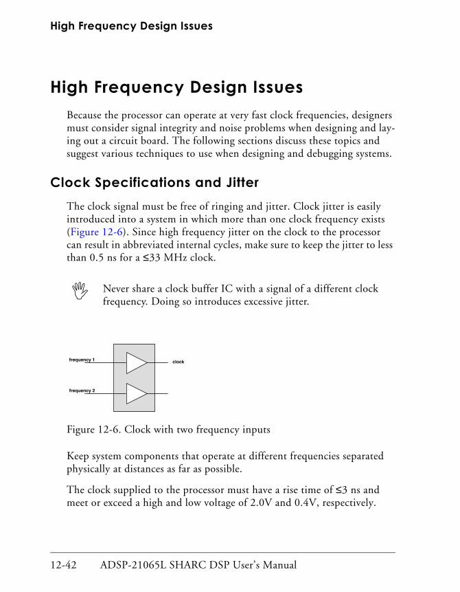
High Frequency Design Issues
12-42 ADSP-21065L SHARC DSP User’s Manual
High Frequency Design IssuesBecause the processor can operate at very fast clock frequencies, designers must consider signal integrity and noise problems when designing and lay-ing out a circuit board. The following sections discuss these topics and suggest various techniques to use when designing and debugging systems.
Clock Specifications and JitterThe clock signal must be free of ringing and jitter. Clock jitter is easily introduced into a system in which more than one clock frequency exists (Figure 12-6). Since high frequency jitter on the clock to the processor can result in abbreviated internal cycles, make sure to keep the jitter to less than 0.5 ns for a ≤33 MHz clock.
Figure 12-6. Clock with two frequency inputs
Keep system components that operate at different frequencies separated physically at distances as far as possible.
The clock supplied to the processor must have a rise time of ≤3 ns and meet or exceed a high and low voltage of 2.0V and 0.4V, respectively.
Never share a clock buffer IC with a signal of a different clock frequency. Doing so introduces excessive jitter.
-" .
-"
/
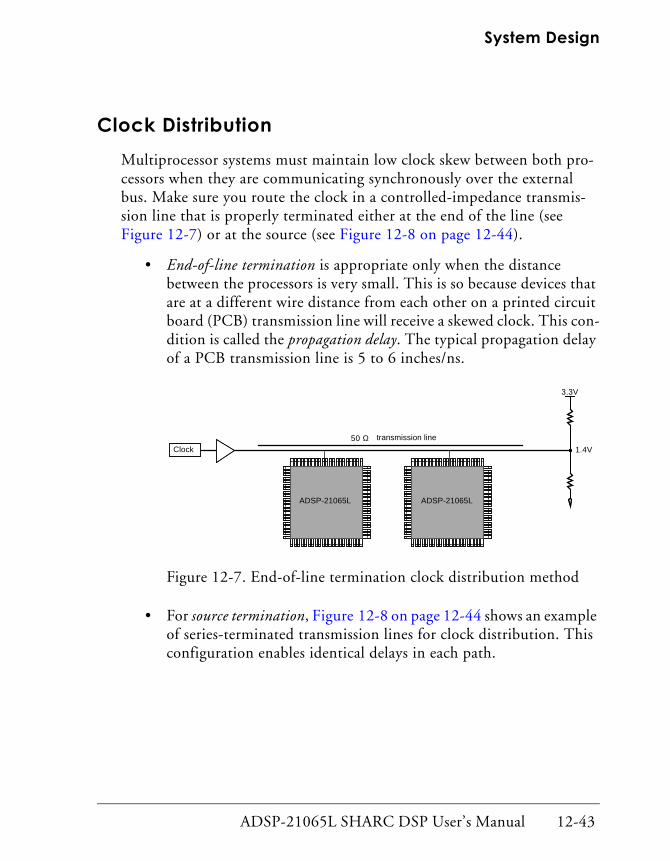
ADSP-21065L SHARC DSP User’s Manual 12-43
System Design
Clock DistributionMultiprocessor systems must maintain low clock skew between both pro-cessors when they are communicating synchronously over the external bus. Make sure you route the clock in a controlled-impedance transmis-sion line that is properly terminated either at the end of the line (see Figure 12-7) or at the source (see Figure 12-8 on page 12-44).
• End-of-line termination is appropriate only when the distance between the processors is very small. This is so because devices that are at a different wire distance from each other on a printed circuit board (PCB) transmission line will receive a skewed clock. This con-dition is called the propagation delay. The typical propagation delay of a PCB transmission line is 5 to 6 inches/ns.
Figure 12-7. End-of-line termination clock distribution method
• For source termination, Figure 12-8 on page 12-44 shows an example of series-terminated transmission lines for clock distribution. This configuration enables identical delays in each path.
ADSP-21065L ADSP-21065L
50 Ω transmission line
1.4V
3.3V
Clock

High Frequency Design Issues
12-44 ADSP-21065L SHARC DSP User’s Manual
Figure 12-8. Source termination clock distribution method
When using source termination, make sure you follow these guidelines:
• Connect each device at the end of the transmission line.
The end of the line is the only point where the signal has a single transition.
• Route the traces so that the delay through each matches the others.
• When using a line impedance higher than 50Ω, keep clock signal traces in the PCB layer closest to the ground plane, so delays remain stable and crosstalk low.
• When placing more than one device at the end of the line, keep the wire length between them short and their impedance (capacitance) high.
• Place the matched inverters in the same IC and specify them for a low skew (<1 ns) with respect to each other.
Specify this skew as small as possible since it subtracts from the mar-gin on most specifications.
ADSP-21065L
ADSP-21065L50 ? transmission line
40 ?
Clock
40 ?
50 ? transmission line
buffe
rdr
ive
impe
danc
e=
10?

ADSP-21065L SHARC DSP User’s Manual 12-45
System Design
Point-to-Point Connections on Serial PortsAlthough you can operate the processor’s serial ports at a slow rate, the output drivers still have fast edge rates and, for longer distances, might require source termination.
You can add a series termination resistor near the pin for point-to-point connections. Typically, serial port applications use this termination method when distances are greater than six inches. For details, see the pro-cessor’s data sheet. For more information on transmission line termination, see “Recommended Reading” on page 12-47.
Signal IntegrityWe recommend that you try to reduce the capacitive loading on high-speed signals as much as possible. Using a buffer for devices that operate with wait states, you can reduce the load on buses. This in turn reduces the capacitance on signals tied to zero-wait-state devices, allowing these signals to switch faster with fewer noise-producing current spikes.
To reduce ringing, minimize the signal run length (inductance). Take extra care with certain signals, such as the read and write strobes (RD, WR) and acknowledge (ACK). In a multiprocessor system, since each pro-cessor can drive the read or write strobes, we recommend that you add some damping resistance in the signal path if the line length is greater than six inches. Doing so, however, will incur additional signal delay. Make sure you carefully analyze the time budget for these signals.
Other Recommendations and Suggestions• Use more than one ground plane on the PCB to reduce crosstalk.
Be sure to use lots of vias between the ground planes. One VDD plane is sufficient. Place these planes in the center of the PCB.

High Frequency Design Issues
12-46 ADSP-21065L SHARC DSP User’s Manual
• To reduce crosstalk, keep critical signals such as clocks, strobes, and bus requests on a signal layer next to a ground plane and away from or perpendicular to other non-critical signals.
For example, data outputs switch at the same time that the processor samples BRx inputs. If your layout permits crosstalk between them, your system could have problems with bus arbitration.
• If possible, position the processors on both sides of the board to reduce area and distances.
• Lower transmission line impedances reduce crosstalk and provide better control of impedance and delay.
• Experiment with the board and isolate crosstalk and noise issues from reflection issues.
To do so, drive a signal wire from a pulse generator and study the reflections while other components and signals are passive.
Decoupling Capacitors and Ground PlanesUse planes for the ground and power supplies.
We recommend that you use a minimum of eight bypass capacitors (0.02 µF ceramic), placed very close to the VDD pins of the package (see Figure 12-9 on page 12-47). Use short and fat traces for this. Tie the ground end of the capacitors directly to the ground plane. Tie the positive (+) end of each capacitor directly to the power plane, as near as possible to the processor’s VDD pins. We recommend a surface-mount capacitor because of its lower series inductance.
Connect the power plane to the power supply pins directly, with mini-mum trace length. To avoid reducing their effectiveness, make sure the

ADSP-21065L SHARC DSP User’s Manual 12-47
System Design
ground planes are not densely perforated with vias or traces. In addition, populate the board with several large tantalum capacitors.
Figure 12-9. Bypass capacitor placement
Oscilloscope ProbesWhen making high-speed measurements, use a “bayonet” or similarly short (< 0.5 inch) ground clip attached to the tip of the oscilloscope probe. Use a low-capacitance active probe with 3 pF or less of loading. If you use a standard ground clip with four inches of ground lead, you will see ringing on the displayed trace and the signal will appear to have exces-sive overshoot and undershoot. To see signals accurately, you need a 1 GHz or better sampling oscilloscope.
Recommended ReadingFor further reading, we recommend the following books. These books are technical references that cover the problems encountered in state-of-the-art, high-frequency digital circuit design, and are excellent sources of practical ideas for problem solving.
Buchanan, James E. Signal and Power Integrity in Digital Systems; TTL, CMOS, & BICMOS. McGraw-Hill. ISBN 0-07-008734-2
Johnson and Graham. High-Speed Digital Design: A Handbook of Black Magic. Prentice Hall, Inc. ISBN 0-13-395724-1
ADSP-21065L
High Frequency Design Issues
12-48 ADSP-21065L SHARC DSP User’s Manual
These books cover these topics:
• High-Speed properties of logic gates
• Measurement techniques
• Transmission lines
• Ground planes and layer stacking
• Terminations
• Vias
• Power systems
• Connectors
• Ribbon cables
• Clock Distribution
• Clock Oscillators

ADSP-21065L SHARC DSP User’s Manual 12-49
System Design
BootingYou can automatically download programs to the processor’s internal memory after power-up or after a software reset. This process is called booting.
The processor supports these boot modes:
• EPROM boot mode
The processor reads data from an 8-bit external EPROM through the external port.
• Host boot mode
The processor accepts data from an 8-, 16-, or 32-bit host micropro-cessor or other external device.
Each boot mode packs boot data into 48-bit instructions and uses DMA channel 8 to transfer the instructions to internal memory.
You use the primary configuration of DMA channel 8 (and EPB0) for EPROM and host booting. The DMAC0 control register is specially ini-tialized for booting in each case.
With either boot method, after the boot process loads 256 words into memory locations 0x8000 through 0x80FF, the processor begins executing instructions. Because most applications require more than 256 words of instructions and initialization data, these 256 words typically serve as a loading routine for the application. Analog Devices supplies a loading rou-tine (Loader Kernel) that can load an entire program. This routine comes with the development tools. For details, see the documentation for the development tools.
The processor also has a no boot mode. In this mode, the proces-sor starts executing instructions from address 0x0002 0004 in external memory.

Booting
12-50 ADSP-21065L SHARC DSP User’s Manual
Selecting the Boot ModeUsed in conjunction, the BMS and BSEL pins select the processor’s boot mode as shown in Table 12-15 and Table 12-16.
Table 12-15. Boot mode pins
Pin Type Description
BMS I/O/Z1
1 Hi-Z only in EPROM boot mode, when pin is an output.
Boot Memory Select mode.
• When BSEL is low, BMS is an input pin, and it selects between Host boot mode and Nonboot mode (the processor executes from external memory).
For No boot mode, connect BMS to ground.
For Host boot mode, connect BMS to VDD.
• When BSEL is high, BMS is an output pin, and the processor starts up in EPROM boot mode.
Connect BMS to the EPROM’s chip select.
BSEL I EPROM Boot Select mode.
Because this signal is a system configuration selection, we recommend that you hardwire it.
• When BSEL is high, the processor starts up in EPROM boot mode.
The processor assumes the EPROM’s data bus is 8-bits wide.
Connect BSEL to the processor’s data bus in LSB alignment.
• When BSEL is low, BMS determines the booting mode.
Connect BSEL to ground.

ADSP-21065L SHARC DSP User’s Manual 12-51
System Design
For either of the power-up boot modes, the processor does not execute the instruction at address 0x0000 8004 during the boot sequence. So, make sure your application does not use that address for loading the kernel.
EPROM BootingSetting the BSEL input high and the BMS input low selects EPROM booting through the external port.
You must connect the byte-wide boot EPROM to DATA7-0. Connect the lowest address pins of the processor to the EPROM’s address lines. Con-nect the EPROM’s chip select to BMS and its output enable to RD.
In a multiprocessor system, only the master processor drives the BMS out-put. This enables you to wire-OR both BMS signals for a single, common boot EPROM.
You can boot both processor's from a single EPROM, using the same code or different code for each processor.
Table 12-16. Boot mode pin configurations
BSEL BMS Description
0 0 No boot mode.
The processor executes from external memory at location 0x20004.
0 1 Host boot mode.
The processor defaults to an 8-bit host bus width.
1 output EPROM boot mode.
The processor assumes an 8-bit EPROM data bus width.
Connect to the data bus in LSB alignment.

Booting
12-52 ADSP-21065L SHARC DSP User’s Manual
During reset, a 2 kΩ equivalent resistor pulls the processor’s ACK line high internally, and an internal keeper latch holds it high. So, you do not need to use an external pull-up resistor on the ACK line at any time.
Bootstraping (256 instructions)
In EPROM boot mode, the external port DMA channel 8 (DMAC0) becomes active following reset.
DMAC0 initializes to 0x02A1 to:
• Enable external port DMA.
• Select DTYPE for instruction words.
• Ignore packing mode bits (PMODE) and force 8-to-48 bit packing with least-significant-word first.
The RBWS and RBWM fields of the WAIT register initialize to generate six wait states (seven cycles total) for the EPROM access in external mem-ory. (Wait states defined for external memory banks are applied to BMS-asserted accesses.)
The RBWM field's initial value selects internal wait and external acknowl-edge. Initially, the processor asserts ACK (high), but if another device drives ACK low during EPROM boot, the processor could latch ACK low. The processor responds to the deasserted (low) ACK as a hold off from the EPROM, inserting wait states continually and preventing completion of the EPROM boot. To avoid this type of boot hold off, set the value of RBWM in the WAIT register to internal wait mode (01) early in the 256 word boot process.
Table 12-17 on page 12-53 shows how the parameter registers for DMAC0 initialize at reset for EPROM booting. The count register (CEP0) initializes to 0x0100 for transferring 256 words to internal mem-ory. The external count register (ECEP0), which the DMA controller uses

ADSP-21065L SHARC DSP User’s Manual 12-53
System Design
to generate external addresses, initializes to 0x0600 (that is, 0x0100 words with six bytes per word).
At system start-up, when the processor’s RESET input goes inactive, the following sequence occurs:
1. The processor goes into an idle state identical to that initiated by the IDLE instruction.
The processor sets the program counter (PC) to address 0x0000 8004.
2. The DMA parameter registers for DMA channel 8 initialize to the values in Table 12-17).
3. BMS becomes the boot EPROM chip select.
4. Eight-bit master mode DMA transfers from EPROM to internal memory begin on the external port data (EPD) lines 7:0.
Table 12-17. DMAC0 parameter register initialization
Register Initialization Value
IIEP0 0x0000 8000
IMEP0 Uninitialized. Value increments +1 automatically
CEP0 0x0100 (256 instruction words)
CPEP0 Unintialized
GPEP0 Unintialized
EIEP0 0x8000 0000
EMEP0 Uninitialized. Value increments +1 automatically
ECEP0 0x0600 (256 words × 6 bytes/word)
Booting
12-54 ADSP-21065L SHARC DSP User’s Manual
5. The external address lines (ADDR23-0) start at 0x000000 and incre-ment after each access.
6. The RD strobe asserts the same as in normal memory accesses, with six wait states (seven cycles).
The processor’s DMA controller continues to read the 8-bit EPROM words, pack them into 48-bit instruction words, and transfer them to internal memory, until it has loaded 256 words. The BMS pin automati-cally selects the EPROM, and the processor disables the other memory select pins. The DMA external count register (ECEP0) decrements after each EPROM transfer.
When ECEP0 reaches zero (0), the processor:
1. Stops DMA transfers.
2. Activates the external port DMA channel 8 interrupt (EP0I).
3. Deactivates BMS and activates normal external memory selects.
4. Vectors to the EP0I interrupt vector at 0x0000 8040.
At this point, the processor has completed its boot sequence and is execut-ing instructions normally.
Make sure the first instruction at the EP0I interrupt vector location, address 0x0000 8040, is an RTI (Return from Interrupt). This instruction returns execution to the reset routine at location 0x0000 8005, where nor-mal program execution can resume. After this, your application can write a different service routine at the EP0I vector location 0x0000 8040.
Remember, for either of the power-up boot modes, the processor does not execute the instruction at address 0x0000 8004 during the boot sequence. So, make sure your application does not use that address for loading the kernel.
ADSP-21065L SHARC DSP User’s Manual 12-55
System Design
Loading the Remaining EPROM Data
The EPROM boot mode only loads 256 instructions during bootstraping. If you must load your entire application into internal memory from the EPROM, the processor must access the boot EPROM after bootstraping has finished. To do so, you use the BSO (Boot Select Override) bit in the SYSCON register.
Setting BSO=1 overrides the external memory selects and asserts the BMS pin for an external port DMA transfer. Code your bootstrap program to set the BSO bit in SYSCON first and then set up an external port DMA channel to read the rest of the EPROM’s contents.
Setting BSO=1 disables the PMODE packing mode bits in the DMAC0 (DMA channel 8) control register and forces 8-to-48 bit packing for reads. (Except for host transfers, eight-bit packing is available only during EPROM booting or on DMA reads when BSO=1.) While one external port DMA channel is operating with BSO=1, you cannot use the other external port DMA channel for non-BMS accesses.
When BSO=1, only a DMA transfer, not an access by the processor’s core, asserts BMS. So, your bootstrap program, if it is running on the proces-sor’s core, can perform other external accesses to nonboot memory.
With BSO=1, you can also use external port DMA channel 9 for DMA reads or writes. With DMA channel 9, you can use any of the PMODE bit modes, but not 8-bit packing. DMA channel 9 provides a way to boot from a wider (16- or 32-bit) ROM for a faster boot, but this requires a custom loader kernel.

Booting
12-56 ADSP-21065L SHARC DSP User’s Manual
Writing to BMS Memory Space
You can also write to processor’s BMS space using the boot select override (BSO mode). The BSO bit in the SYSCON register enables software to assert the BMS pin. In many systems, applications may need to update or modify the boot data. In such systems, a writable EEPROM or FLASH memory may substitute for the EPROM.
To write to memory with the BMS line asserted, use DMA channel 9, not DMA channel 8. With BSO=1, use DMA channel 8 only for reads. This access limitation occurs because DMA channel 8 is hardwired for a special 8-bit boot read mode. When BSO=1, a write with DMA channel 8 results in illegal chip operation.
When BSO=1, you can use DMA channel 9 with any of the modes available in the DMACx register for reads or writes, with any packing mode, and with any data or instructions. Because BMS space is 8-bits wide and no 8-bit packing mode is available for these writes, you must use the Shifter to place data in the correct location for each write.
Booting From the HostBooting the processor from a 8-bit host occurs over the external port’s data and address buses. The processor’s BSEL and BMS pin select between EPROM booting and host booting. For host booting, BSEL must be low and BMS high.
Configured for host booting, the processor enters slave mode after reset and waits for the host to download the boot program.
After reset, the processor goes into an idle state identical to that initiated by the IDLE instruction, with the program counter (PC) set to address 0x0000 8004. The parameter registers for external port DMA channel 8 initialize as shown in Table 12-18 on page 12-57, but no DMA transfers start.
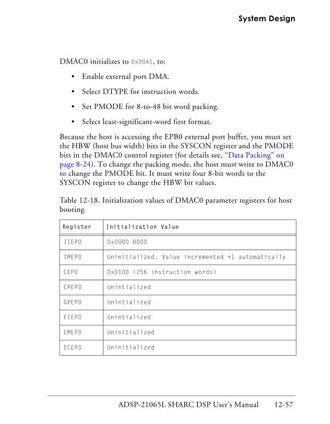
ADSP-21065L SHARC DSP User’s Manual 12-57
System Design
DMAC0 initializes to 0x00A1, to:
• Enable external port DMA.
• Select DTYPE for instruction words.
• Set PMODE for 8-to-48 bit word packing.
• Select least-significant-word first format.
Because the host is accessing the EPB0 external port buffer, you must set the HBW (host bus width) bits in the SYSCON register and the PMODE bits in the DMAC0 control register (for details see, “Data Packing” on page 8-24). To change the packing mode, the host must write to DMAC0 to change the PMODE bit. It must write four 8-bit words to the SYSCON register to change the HBW bit values.
Table 12-18. Initialization values of DMAC0 parameter registers for host booting
Register Initialization Value
IIEP0 0x0000 8000
IMEP0 Uninitialized. Value incremented +1 automatically
CEP0 0x0100 (256 instruction words)
CPEP0 Unintialized
GPEP0 Unintialized
EIEP0 Unintialized
EMEP0 Uninitialized
ECEP0 Uninitialized

Booting
12-58 ADSP-21065L SHARC DSP User’s Manual
The host asserts the processor’s HBR input to initiate the boot operation. After the host receives the HBG signal from the processor, it can perform one of two actions:
• Write directly to EPB0, the external port DMA buffer 0 (which cor-responds to DMA channel 8) to start downloading instructions.
• Write to any of the IOP control registers to change the processor’s reset initialization conditions. To do so, the host must use DATA7-0 or, if HBW is configured for a 16-bit host, DATA15-0.
When the processor’s DMA controller has downloaded 256 instructions, the processor:
1. Stops DMA transfers.
2. Activates the external port DMA channel 8 interrupt (EP0I).
3. Vectors to the EP0I interrupt vector at 0x0000 8040.
Make sure the first instruction at the EP0I interrupt vector location, address 0x0000 8040, is an RTI (Return from Interrupt). RTI returns exe-cution to the reset routine at location 0x0000 8005 to resume normal program execution. After that, your application can write a different ser-vice routine at the EP0I vector location 0x0000 8040. These 256 instructions must load the rest of your program.
Because only external port DMA channel 8 has its IMASK bit set to enable a DMA done interrupt, you must use this channel for the initial instruction download.
Multiprocessor BootingYou can boot multiprocessor systems from a host or from an external EPROM.

ADSP-21065L SHARC DSP User’s Manual 12-59
System Design
Multiprocessor Host Booting
To boot two processors from a host, you must configure each processor’s BSEL and BMS pins for host booting: BSEL = 0 and BMS = 1
After system power-up, each processor is in the idle state, and the BRx bus request lines are high. To boot each processor, the host must assert the HBR input, assert each processor’s CS pin, and download instructions as described in “Booting From the Host” on page 12-56.
Multiprocessor EPROM Booting
In a multiprocessor system, to boot sequentially from one EPROM, both processors:
• Arbitrate for the bus.
• DMA transfer the 256 word boot stream after becoming bus master.
• Release the bus.
• Execute the loaded instructions.
To drive the chip select pin of the EPROM, you can wire-OR together the BMS signals from both processors. The processors can boot in turn, according to their priority. The last one to finish booting must inform the other (which may be in the idle state) that program execution can begin (if both processors intend to start executing instructions simultaneously).
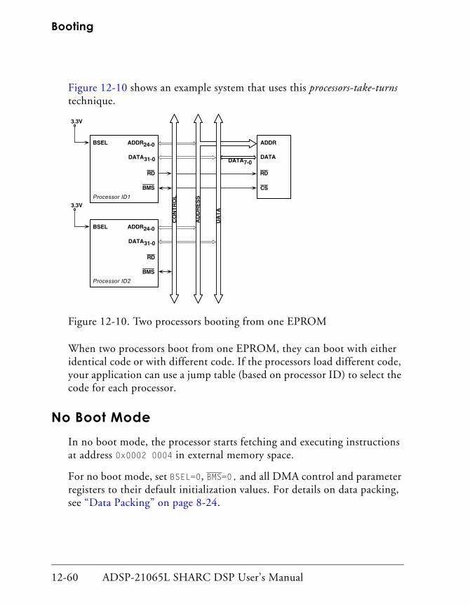
Booting
12-60 ADSP-21065L SHARC DSP User’s Manual
Figure 12-10 shows an example system that uses this processors-take-turns technique.
Figure 12-10. Two processors booting from one EPROM
When two processors boot from one EPROM, they can boot with either identical code or with different code. If the processors load different code, your application can use a jump table (based on processor ID) to select the code for each processor.
No Boot ModeIn no boot mode, the processor starts fetching and executing instructions at address 0x0002 0004 in external memory space.
For no boot mode, set BSEL=0, BMS=0, and all DMA control and parameter registers to their default initialization values. For details on data packing, see “Data Packing” on page 8-24.
0& 123
4.23
0$
0& 123
4.23
0$
44
44
&
%5%
623

ADSP-21065L SHARC DSP User’s Manual 12-61
System Design
Locating the Interrupt Vector TableIf the processor boots externally from an EPROM or from the host, the interrupt vector table is located in internal memory space. If the processor does not boot, but executes from external memory, the vector table must be located in the external memory space.
You can use the IIVT bit in the SYSCON register to override the location of the interrupt vector table when the processor is configured for no boot mode:
IIVT=0 Located in external memory at 0x0002 0000
IIVT=1 Located in internal memory at 0x0000 8000
If the processor boots from an external source (any mode other than no boot mode), IIVT has no effect.
IIVT defaults to zero (0).

Data Delays, Latencies, and Throughput
12-62 ADSP-21065L SHARC DSP User’s Manual
Data Delays, Latencies, and ThroughputTable 12-19 specifies, in number of 2xCLKIN cycles, data delays and throughput for the processor, excluding SDRAM operations. Table 12-20 on page 12-64 specifies, in number of 2xCLKIN cycles, data delays and throughput for SDRAM operations. Table 12-21 on page 12-65 specifies, in number of 2xCLKIN cycles, latencies and throughputs for the processor.
Data delay and latency are the number of 2xCLKIN cycles (after the first cycle) required to complete an operation. So, a zero-wait-state memory has a data delay of zero (0) cycles, and a single-wait-state memory has a data delay of one (1) cycle.
Throughput is the maximum rate in 2xCLKIN cycles at which the proces-sor performs an operation. Data delay and throughput are the same whether the access is from a host or from another processor.
Table 12-19. Data delays and throughputs
Operation Min. Delay
Max. Throughput
Core accesses to external memory space 0 2
Syn. accesses to slave’s IOP registers1
Read (transfer out)
Write (transfer in)
0
42,3
4
2
Slave mode DMA transfers
Read (transfer out)
Write (transfer in)
—
—
44
2
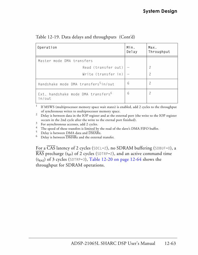
ADSP-21065L SHARC DSP User’s Manual 12-63
System Design
For a CAS latency of 2 cycles (SDCL=2), no SDRAM buffering (SDBUF=0), a RAS precharge (tRP) of 2 cycles (SDTRP=2), and an active command time (tRAS) of 3 cycles (SDTRP=3), Table 12-20 on page 12-64 shows the throughput for SDRAM operations.
Master mode DMA transfers
Read (transfer out)
Write (transfer in)
—
—
2
2
Handshake mode DMA transfers5in/out 6 2
Ext. handshake mode DMA transfers6
in/out6 2
1 If MSWS (multiprocessor memory space wait states) is enabled, add 2 cycles to the throughput of synchronous writes to multiprocessor memory space.
2 Delay is between data in the IOP register and at the external port (the write to the IOP register occurs in the 2nd cycle after the write to the eternal port finished).
3 For asynchronous accesses, add 2 cycles.4 The speed of these transfers is limited by the read of the slave’s DMA FIFO buffer.5 Delay is between DMA data and DMARx.6 Delay is between DMARx and the external transfer.
Table 12-19. Data delays and throughputs (Cont’d)
Operation Min. Delay
Max. Throughput
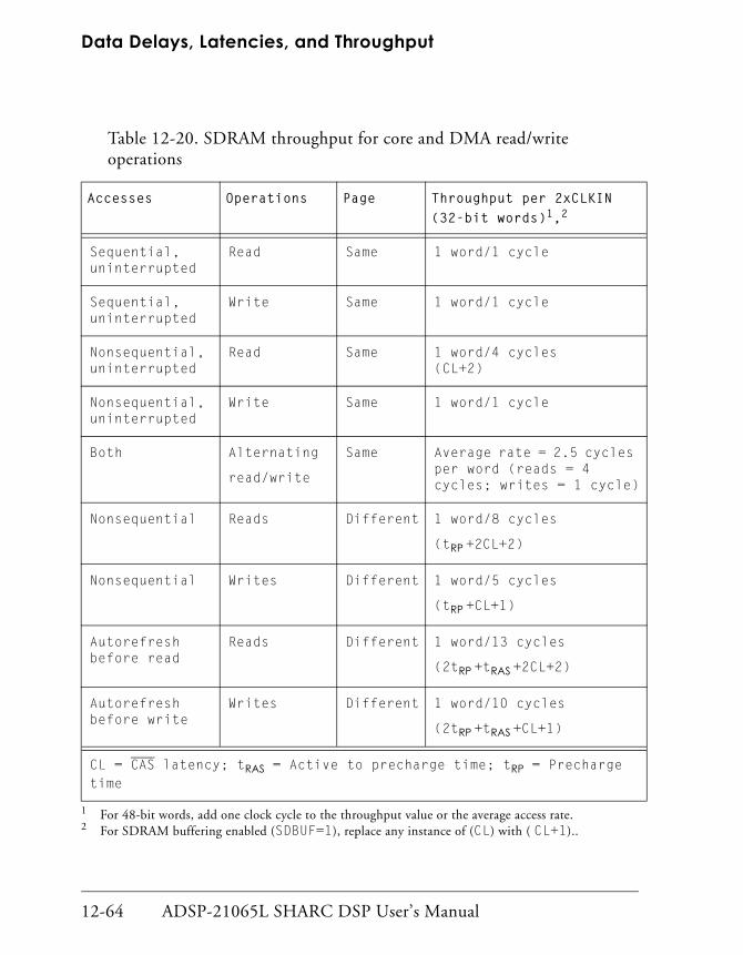
Data Delays, Latencies, and Throughput
12-64 ADSP-21065L SHARC DSP User’s Manual
Table 12-20. SDRAM throughput for core and DMA read/write operations
Accesses Operations Page Throughput per 2xCLKIN (32-bit words)1,2
Sequential, uninterrupted
Read Same 1 word/1 cycle
Sequential, uninterrupted
Write Same 1 word/1 cycle
Nonsequential,uninterrupted
Read Same 1 word/4 cycles(CL+2)
Nonsequential, uninterrupted
Write Same 1 word/1 cycle
Both Alternating
read/write
Same Average rate = 2.5 cycles per word (reads = 4 cycles; writes = 1 cycle)
Nonsequential Reads Different 1 word/8 cycles
(tRP +2CL+2)
Nonsequential Writes Different 1 word/5 cycles
(tRP +CL+1)
Autorefresh before read
Reads Different 1 word/13 cycles
(2tRP +tRAS +2CL+2)
Autorefresh before write
Writes Different 1 word/10 cycles
(2tRP +tRAS +CL+1)
CL = CAS latency; tRAS = Active to precharge time; tRP = Precharge time
1 For 48-bit words, add one clock cycle to the throughput value or the average access rate.2 For SDRAM buffering enabled (SDBUF=1), replace any instance of (CL) with ( CL+1)..

ADSP-21065L SHARC DSP User’s Manual 12-65
System Design
Table 12-21. Latencies and throughputs
Operation Min. Latency
Max. Throughput
Interrupts (IRQ2-0) 3 NA
Multiprocessor bus requests (BR2-1) 2 NA
Host bus request (HBR) 2 NA
SYSCON effect latency 1 NA
Host packing status update (SYSTAT) 0 NA
DMA packing status update (DMACx) 1 NA
DMA chain initialization 7-11 NA
Vector interrupt (VIRPT) 6 NA
Serial ports1 70 64
1 32-bit words, processor core to processor core.

Execution Stalls
12-66 ADSP-21065L SHARC DSP User’s Manual
Execution StallsTable 12-22 lists the events that can stall program execution in the proces-sor’s core and the length of the stall in number of 2xCLKIN cycles.
Table 12-22. Events that cause core components to stall
Component Cycles Cause
DAGs 1 Register conflict
DMA 1 Accessing a DMA parameter register dur-ing DMA address generation. For example, writing to the register during a regis-ter update, or reading
1 Accessing a DMA parameter register dur-ing DMA chaining.
n Writing/reading a DMA buffer that is full/empty.
IOPRegisters
n Both PM and DM buses accessing IOP reg-isters. Both must complete their access.
n Conflict with slave access.

ADSP-21065L SHARC DSP User’s Manual 12-67
System Design
Memory 1 Both the PM and DM data buses accessing the same block of internal memory.
n Conflicting accesses of external memory. Stalls until the PM and DM buses com-plete their accesses.
n Accesses to external memory. Stalls until the I/O buffers are cleared.
n External accesses when the processor does not own the external bus.
n External accesses. Stalls until access finishes (wait states, idle cycles, …)
Program Sequencer
1 Accesses of program data memory with cache miss.
2 Nondelayed branches.
2 Normal interrupts.
5 Vector interrupt (VIRPT)
1 Short loops with small iterations.
n IDLE instruction.
Table 12-22. Events that cause core components to stall (Cont’d)
Component Cycles Cause

Execution Stalls
12-68 ADSP-21065L SHARC DSP User’s Manual
ADSP-21065L SHARC DSP User’s Manual 13-1
13 PROGRAMMING CONSIDERATIONS
Figure 13-0.
Listing 13-0.
Table 13-0.
This chapter summarizes important information to keep in mind when you write application software for the ADSP-21065L.
Extra Cycle ConditionsAll instructions can execute in a single cycle but may take longer under certain conditions:
• Nondelayed branches
• Accesses of program memory data with cache miss
• Loop accesses of program memory data
• Execution of one- and two-instruction loops
• Writes to DAG registers
• Wait state programming
Nondelayed BranchesA nondelayed branch instruction (JUMP, CALL, RTS or RTI) fetches but does not execute the next two instructions. The processor aborts execution of the next two instructions and executes two NOPs instead.
To avoid this two-cycle delay, your application can use a delayed branch, which executes the next two instructions after it before the branch opera-tion actually occurs. In this case, because the processor executes the two

Extra Cycle Conditions
13-2 ADSP-21065L SHARC DSP User’s Manual
extra instructions before taking the branch, program flow deviates from the apparent order of operations.
For details, see Chapter 3‚ Program Sequencing.
Program Memory Data Accesses with Cache MissThe processor checks the instruction cache on every program memory data access. If the needed instruction is in the cache, the fetch from the cache occurs in parallel with the PM bus data access, and the instruction executes in a single cycle. However, if the Program Sequencer does not cache the instruction, the processor must wait for the PM bus data access to finish before it can fetch the next instruction. This results in a mini-mum delay of one cycle. However, a PM bus data access that uses external memory with wait states can increase this delay. This delay occurs even if the PM bus data access is based on a conditional that evaluates to false.
For details, see Chapter 3‚ Program Sequencing.
Loop Accesses of Program Memory DataDuring the execution of a PM bus data access, the processor caches an instruction that it needs to fetch. Because of the execution pipeline, this instruction is usually two memory locations after the PM bus data access. If the PM bus data access is in a loop, a cache miss usually occurs on the first iteration of the loop, and cache hits occur on subsequent iterations. This results in one extra cycle during execution of the loop.
However, certain cases require fetching different instructions from the cache during different iterations. In these cases, the number of cache misses, and therefore the number of extra cycles, increases. Table 13-1 on page 13-3 lists these special cases. The values listed in this table are based on the worst-case scenario, so actual performance of the cache for a given application may be higher.

ADSP-21065L SHARC DSP User’s Manual 13-3
Programming Considerations
Two Misses. If the program memory data access occurs in the last two instructions of a loop, a cache miss always occurs on the first and last iter-ations of the loop to add two extra cycles.
On the first iteration, the processor needs to fetch the first or second instruction from the top of the loop.
On the last iteration, the processor needs to fetch one of the two instruc-tions following the loop.
At each of these points, a cache miss occurs the first time the code con-taining the loop executes.
Three Misses. If a loop contains only one instruction, and that instruction requires a PM bus data access, three cache misses can occur.
On the first iteration, if the loop iterates three times or more, the proces-sor needs to fetch the loop instruction again.
On the next-to-last iteration, the processor needs to fetch the next instruc-tion after the loop.
On the last instruction, the processor needs to fetch the second instruction after the loop.
In each case, a cache miss occurs the first time the code containing the loop executes.
Table 13-1. Cases that increase cache misses and extra cycles
Misses # Instructions Address of PM Data Access
0 >2 Not at e or (e −1)
1 ≥2 At e or (e −1)
2 1 At the single loop location
e = loop end address
Extra Cycle Conditions
13-4 ADSP-21065L SHARC DSP User’s Manual
For details, see Chapter 3‚ Program Sequencing.
Using One- and Two-Instruction LoopsCounter-based loops that have only one or two instructions can cause delays if they do not execute a minimum number of times. The processor checks the termination condition two cycles before it exits the loop. In short loops, the processor has already looped back when it tests the termi-nation condition. So, if the termination condition tests true, the processor must abort the two instructions in the pipeline and execute NOPs instead.
Specifically, executing a one-instruction loop one or two times or execut-ing a two-instruction loop only once incurs two cycles of overhead because both loops result in two aborted instructions after the last iteration. These overhead cycles are additional to extra cycles that a PM bus data access inside the loop generates. To avoid this kind of overhead, use straight-line code instead of loops.
For details, see Chapter 3‚ Program Sequencing.
Writing to a DAG RegisterWhen an instruction that uses any register in a DAG for data addressing, modifying instructions, or indirectly jumping follows an instruction that writes to the same DAG register, the processor inserts a NOP cycle between the two instructions. It does so because both operations need the same bus in the same cycle, and it must delay the second operation. For example:
L2=8;DM(I0,M1)=R1;
Because L2 is in the same DAG as I0 (and M1), the processor inserts an extra cycle after the write to L2.
For details, see Chapter 4‚ Data Addressing.

ADSP-21065L SHARC DSP User’s Manual 13-5
Programming Considerations
Programming Wait StatesYou can program an external memory access to include a specific number of wait states and bus idle cycles and to wait for an external ACK signal before completing the access.
If you program internal wait states and bus idle cycles only, the length of the delay is exactly the number of wait states and bus idle cycles (1 wait state = 1 cycle).
If you program the external ACK signal, either alone or in combination with programmed wait states, the length of the delay varies depending on the external system.
For details, see Chapter 5‚ Memory.
Component Considerations
13-6 ADSP-21065L SHARC DSP User’s Manual
Component ConsiderationsOther programming considerations include operations that interact with specific processor components:
• Computation units
• Data Address Generators
• Memory
Computation UnitsFor detailed information on the processor’s computation units, see Chapter 2‚ Computation Units. Programming considerations include:
• Compute operations
• Restrictions on delayed branching
• Writing twice to the same location in the Register File
Compute Operations
In fixed-point to floating-point conversion, the rounding boundary is always 40 bits even if the RND32 bit is set.
The ALU Zero flag (AZ) signifies floating-point underflow as well as a zero result.
Transfers between MR registers and the Register File are considered mul-tiplier operations. For details, see Appendix E‚ Control and Status Registers, in ADSP-21065L SHARC DSP Technical Reference.

ADSP-21065L SHARC DSP User’s Manual 13-7
Programming Considerations
Restrictions on Delayed Branching
The processor executes sequentially a delayed branch instruction and the next two consecutive instructions. The processor delays servicing any interrupt that occurs between a delayed branch instruction and either of the next two consecutive instructions until it completes the branch.
You can use delayed branching with the JUMP, CALL, RTS, and RTI instructions with some restrictions.
For delayed JUMPs, you cannot use these instructions in the two locations immediately following the jump:
• Other JUMP, CALL, RTS, or RTI instructions
• DO UNTIL
For delayed CALL, RTS, or RTI operations, you cannot use these instruc-tions in the two locations immediately following the CALL, RTS, or RTI instruction:
• Other JUMP, CALL, RTS, or RTI instructions
• DO UNTIL
• Pushes and pops of the PC stack
• Writes to the PC stack or PC stack pointer
Writing Twice to the Same Location in the Register File
If two writes to the same Register File location take place in the same cycle, only the write with higher precedence actually occurs. The source of the write data determines the precedence of the writer operation.

Component Considerations
13-8 ADSP-21065L SHARC DSP User’s Manual
From highest to lowest, the order of precedence is:
• Data memory (DM bus) or universal register
• Program memory (PM bus)
• ALU
• Multiplier
• Shifter
Data Address GeneratorsFor detailed information on the processor’s data address generators (DAGs), see Chapter 4‚ Data Addressing. Programming considerations include:
• Illegal DAG register transfers
• Initializing circular buffers
Illegal DAG Register Transfers
The following instructions execute, but cause incorrect results. The assem-bler does not support these instructions:
• An instruction that stores a DAG register in memory using indirect addressing from the same DAG, with or without updating the index register (I).
In this case, the instruction writes the wrong data to memory or updates the wrong index register.
DM(M2,I1)=I0; or DM(I1,M2)=I0;
ADSP-21065L SHARC DSP User’s Manual 13-9
Programming Considerations
• An instruction that loads a DAG register from memory using indi-rect addressing from the same DAG and updates the I index register.
In this case, the instruction either loads the DAG register or updates the index register, but not both.
L2=DM(I1,M0);
Initializing Circular Buffers
To set up a circular buffer, you initialize an L register with a positive, non-zero value and load the corresponding (same-numbered) B register with the base address of the buffer.
The base address, or starting address, is the lowest address of the buffer.
The processor automatically loads the corresponding I (index) register with the same starting address.
MemoryFor detailed information on the processor’s on-chip SRAM memory, see Chapter 5‚ Memory. Programming considerations include:
• Mixing 32- and 48-bit words in one memory block
• Performing dual data accesses
• Reading 16-bit short words
• Restrictions on memory access space
Performing Dual Data Accesses
The processor’s PM and DM buses enable the processor’s core to simulta-neously access instructions and data from both memory blocks. The processor’s core fetches instructions over the PM bus or from the instruc-

Component Considerations
13-10 ADSP-21065L SHARC DSP User’s Manual
tion cache. The core can access data over both the DM bus (using DAG1) and the PM bus (using DAG2).
You can configure the processor’s two memory blocks to store different combinations of 48-bit instruction words and 32-bit data words. To achieve maximum efficiency (single-cycle execution of dual-data-access instructions), however, configure one block to contain a mix of instruc-tions and PM bus data and configure the other block to contain DM bus data only.
Reading 16-Bit Short Words
The processor automatically extends short words read into universal regis-ters into 32-bit integers. Depending on the value of the SSE bit in the MODE1 register, the processor either zero-fills or sign-extends the upper sixteen bits of the 32-bit integer.
Restrictions on Memory Access Space
With a few limitations, you can use the processor’s three internal buses, PM, DM, and I/O to access the processor’s memory map:
• The DM bus can access all memory spaces.
• The PM bus can access internal memory space and the lowest 15.75 megawords of external memory space only.
• The I/O bus can access all memory spaces except the mem-ory-mapped IOP registers in internal memory space.

ADSP-21065L SHARC DSP User’s Manual I-1
I INDEX
Symbols“Group I Instructions (Compute &
Move)” on page A-28 A-2
Numerics32- and 48-bit memory words, using
5-3032-bit data starting memory address
5-35
AAC (ALU fixed-point carry) bit 2-16
described 2-18fixed-point logic operations and 2-18setting and clearing 2-18
AC condition 3-13Access address fields for external
memory space 5-26Access restrictions
for internal buses 5-27memory space 5-27
Access timingexternal memory space 5-65
bus master reads 5-66bus master writes 5-67diagram of 5-65external bus control 5-65
multiprocessor memory space 5-65, 5-67diagram of 5-68
Accessing data over the PM bus 5-10ACK
EPROM booting 12-52extending off-chip memory accesses
5-53external memory space interface and
5-47IOP register writes and 7-26multiprocessing and 12-52pin definition 12-7single-word EPBx data transfers and
7-28state after reset 12-22
Act command 10-30Address boundaries
external memory space 5-19internal memory space 5-19multiprocessor memory space 5-19reserved addresses 5-19
Address decoding table for memory accesses 5-20
Address ranges for instructions and data 5-34

INDEX
I-2 ADSP-21065L SHARC DSP User’s Manual
Address regions of internal memory space 5-23
Addressing32-bit data starting memory
address 5-35data accesses of external memory
space 5-52direct 5-11immediate 5-11indirect 5-11
ADDRxand host accesses 8-11EPROM booting and 12-54external memory space interface
and 5-44generating addresses outside the
address range of external memory space 6-30
parallel SDRAM refresh command 10-28
pin definition 12-4state after reset 12-22
ADI product information, sources of -xix, -xiii
ADI product literature -xxiv, -xviiiADREDY bit (active drive REDY)
switching between open and active-drain output 8-12
ADSP-21065L block diagram 6-2AF (ALU floating-point operation)
bit 2-16described 2-19
AI (ALU floating-point invalid operation) bit 2-16
described 2-19setting 2-19
AIS (ALU floating-point invalid operation) bit 2-17
described 2-19setting 2-19
Alternate DAG registers 4-3architecture 4-4context switching and 4-3described 4-3diagram of 4-4MODE1 control bits for 4-5SRD1H (DAG1 alternate register
select 7-4) 4-5SRD1L (DAG1 alternate register
select 3-0) 4-5SRD2H (DAG2 alternate register
select 15-12) 4-5SRD2L (DAG2 alternate register
select 11-8) 4-5Alternate register file registers 2-11
context switching 2-11control bits 2-11described 2-11effect latency of activation 2-11selecting the active sets 2-11SRRFH 2-11SRRFL 2-11
ALUdata formats 2-12described 2-1instruction set summary 2-21instruction types 2-12operating modes 2-14
ADSP-21065L SHARC DSP User’s Manual I-3
INDEX
see ALU operating modesstatus flags 2-16
see ALU status flagsALU fixed-point saturation mode
2-14ALU overflow flag and 2-15described 2-14negative overflows 2-15positive overflows 2-14
ALU floating-point rounding boundary 2-15
32-bit IEEE results 2-1540-bit results 2-15fixed- to floating-point conversion
2-15floating-point results, format of
2-15ALU floating-point rounding
modes 2-15round-to-nearest 2-15round-to-zero 2-15
ALU instruction set, summary of 2-21
ALU operating modes 2-14ALUSAT (ALU saturation mode)
bit 2-14fixed-point saturation mode 2-14
see ALU fixed-point saturation mode
MODE1 control bits 2-14RND32 (floating-point rounding
boundary) bit 2-14TRUNC (floating-point
rounding mode) bit 2-14
ALU operationCACC status flag updates 2-16compare accumulate operations
2-19fixed- to floating-point conversion
2-15fixed-point results 2-13floating-point rounding boundary
2-15see ALU floating-point rounding
boundaryfloating-point rounding modes
2-15see ALU floating-point rounding
modesstatus flag updating 2-17
ALU operationsand the register file 2-13fixed-point inputs 2-13fixed-point results, storing 2-13instruction set summary 2-21operands 2-13
ALU single-function compute operations
COMP (Fx, Fy) B-31COMP (Rx, Ry) B-11described B-2fixed-point, summary of B-3floating-point, summary of B-4Fn= -Fx B-32Fn=(Fx+Fy)/2 B-30Fn=ABS (Fx+Fy) B-28Fn=ABS (Fx-Fy) B-29Fn=ABS Fx B-33

INDEX
I-4 ADSP-21065L SHARC DSP User’s Manual
Fn=CLIP Fx BY Fy B-49Fn=FLOAT Rx B-41Fn=FLOAT Rx BY Ry B-41Fn=Fx COPYSIGN Fy B-46Fn=Fx+Fy B-26Fn=Fx-Fy B-27Fn=MAX (Fx, Fy) B-48Fn=MIN (Fx, Fy) B-47Fn=PASS Fx B-34Fn=RECIPS Fx B-42Fn=RND Fx B-35Fn=RSQRTS Fx B-44Fn=SCALB Fx BY Ry B-36Rn= -Rx B-16Rn=(Rx-Ry)/2 B-10Rn=ABS Rx B-17Rn=CLIP Rx BY Ry B-25Rn=FIX Fx B-39Rn=FIX Fx BY Ry B-39Rn=LOGB Fx B-38Rn=MANT Fx B-37Rn=MAX (Rx, Ry) B-24Rn=MIN (Rx, Ry) B-23Rn=NOT Rx B-22Rn=PASS Rx B-18Rn=Rx AND Ry B-19Rn=Rx OR Ry B-20Rn=Rx XOR Ry B-21Rn=Rx+1 B-14Rn=Rx+Cl B-12Rn=Rx+Cl-1 B-13Rn=Rx+Ry B-6Rn=Rx+Ry+Cl B-8Rn=Rx-1 B-15
Rn=Rx-Ry B-7Rn=Rx-Ry+Cl B-9Rn=TRUNC Fx B-39Rn=TRUNC Fx BY Ry B-39
ALU status flags 2-16AC (ALU fixed-point carry) 2-16AF (ALU floating-point
operation) 2-16AI (ALU floating-point invalid
operation) 2-16AIS (ALU floating-point invalid
operation) 2-17AN (ALU result negative) 2-16AOS (ALU fixed-point overflow)
2-17AS (ALU x input sign) 2-16ASTAT status bits, summary of
2-16AUS (ALU floating-point
underflow) 2-17AV (ALU overflow) 2-16AVS (ALU floating-point
overflow) 2-17AZ (ALU result 0 or
floating-point underflow) 2-16CACC (compare accumulation
register) 2-16CACC update timing 2-16dual add/subtract (fixed-point)
B-96dual add/subtract (floating-point)
B-98fixed-point carry flag 2-18floating- to fixed-point

ADSP-21065L SHARC DSP User’s Manual I-5
INDEX
conversions and 2-17floating-point operation flag 2-19invalid flag 2-19negative flag 2-18overflow flags 2-18sign flag 2-19state of 2-16status register writes, priority of
2-17sticky status flags 2-16STKY status bits, summary of
2-17underflow flags 2-17updating 2-17zero flag 2-17
ALUSAT (ALU saturation mode) bit 2-14
AN (ALU result negative) bit 2-16described 2-18
AOS (ALU fixed-point overflow) bit 2-17
described 2-18Arithmetic exceptions 3-38Arithmetic logic (ALU) unit
see ALUArithmetic status register, see
ASTAT registerArray signal processing 5-29AS (ALU x input sign) bit 2-16
ABS and MANT operations 2-19described 2-19
Assembler instruction mnemonics 3-12
ASTAT register 2-16
AC 2-16AF 2-16AI 2-16ALU status flags, summary of
2-16AN 2-16AS 2-16AV 2-16AZ 2-16BFT E-6bit definitions E-10bitwise operations and 11-14BTF 3-12CACC 2-16conditional instructions and 3-12CRBM 7-11default bit values, diagram of E-9described E-8flag status updates 12-31FLAG3-0 11-14, 12-29FLAG3-0 inputs 12-31FLAG3-0 outputs 12-33FLAGx status bits 12-32FLAGxO status bits 12-32initialization value E-8MI 2-34MN 2-34MU 2-34multiplier status bits, summary of
2-34multiplier status flags 2-34multiprocessing and 7-11MV 2-34preserved current values of 3-49

INDEX
I-6 ADSP-21065L SHARC DSP User’s Manual
RTI instruction and 3-16Shifter status bits, summary of
2-45signaling external devices with
FLAGx bits 12-33SS 2-45status stack pushes and pops
12-34status stack save and restore
operations 3-48SV 2-45SZ 2-45
Asynchronous external interruptsdescribed 3-51guarantee sampling 3-51
Asynchronous host transfers 8-9and SDRAM 8-9broadcast writes 8-23
see Broadcast writesCS 8-9host driven signals 8-9
Asynchronous inputs 12-3, 12-27signal recognition phase 12-27synchronization delay 12-27
Asynchronous transfer timing, see Host asynchronous accesses
AUS (ALU floating-point underflow) bit 2-17
described 2-17floating- to fixed-point
conversions and 2-17setting 2-18
Automatic wait state option 5-62AV (ALU overflow) bit 2-16
ALU fixed-point saturation mode and 2-15
described 2-18AV condition 3-13AVS (ALU floating-point overflow)
bit 2-17described 2-18
AZ (ALU result 0 or floating-point underflow) bit 2-16
described 2-17floating- to fixed-point
conversions and 2-17setting 2-17underflow status 2-18
BB (DAG base address) registers 4-2
circular data buffers and 4-11Bank activate command (SDRAM),
see Act commandBCNT register
BTC and 7-18bus lock and 7-18bus mastership timeout counter
7-18HBR and 7-18master processor operation 7-18
BHD (buffer hang disable) bit 8-19, 9-86
single-word EPBx data transfers 7-29
SPORT data buffer read/write results 9-7
SPORT data buffer reads/writes

ADSP-21065L SHARC DSP User’s Manual I-7
INDEX
and 9-15Bit reversal
bit-reverse instruction 4-14see Bit-reverse instruction
bit-reverse mode 4-13see Bit-reverse mode
data addressing 4-13BIT SET instruction
software interrupts, activating 3-49
Bit test flag bit, see BTF bitBit-reverse instruction
BITREV 4-14described 4-14index (I) registers and 4-14operation sequence 4-14
Bit-reverse modecontrol bits, summary of 4-14DAG1 operation 4-13DAG2 operation 4-13described 4-13effect timing 4-14postmodify addressing operations
4-14BM condition 3-13, 3-14BMAX register
bus mastership timeout 7-17maximum value of 7-17
BMS 5-53boot mode 12-50EPROM boot mode 5-53, 12-51EPROM boot sequence after reset
12-53EPROM chip select 12-53
host booting 12-56multiprocessing 12-51multiprocessor EPROM booting
12-59multiprocessor host booting
12-59pin connection 5-53pin definition 12-13state after reset 12-23
BMSTRpin definition 12-13state after reset 12-22
Boot hold off 12-52Boot master output, see BMSTRBoot memory select (BSEL, BMS)
described 5-53EPROM boot mode 5-53pin connections 5-53
Boot memory select, see BMSBoot mode pins
BMS 12-50BSEL 12-50configurations 12-51
Boot modesboot sequence and kernel loading
12-54data packing 12-49EPROM 5-53, 12-49, 12-51
see EPROM boot modehost 12-49, 12-56
see Host boot modeinterrupt vector table address 5-30no boot 5-30, 12-49, 12-60
see No boot mode

INDEX
I-8 ADSP-21065L SHARC DSP User’s Manual
pins, see Boot mode pinsselecting 12-50when IIVT=1 5-30
Boot select override, see BSO (boot select override)
Boot sequence and kernel loading 12-51
Booting 12-49described 12-49host boot sequence 12-58loading an entire program 12-49loading routine 12-49modes, see Boot modesmultiprocessor systems 12-58selecting 12-50
Branch instructionscall 3-16delayed, see Delayed branchesdescribed 3-16jump 3-16nondelayed, see Nondelayed
branchesparameters 3-16program memory data accesses
3-11RTI 3-16RTS 3-16
Broadcast writesCS 8-23defined 8-23implementing 8-23REDY 8-23
BRxBTC and 7-12, 8-8
connection in a multiprocessor system 7-3
multiprocessor bus arbitration 7-10
pin definition 12-14state after reset 12-22system bus acquisition 7-12
BSEL 5-53boot mode 12-50EPROM boot mode 5-53host booting 12-56multiprocessor host booting
12-59pin connection 5-53pin definition 12-14state after reset 12-23
BSO (boot select override)accessing EPROM after bootstrap
12-55overriding BMS 12-55writing to BMS memory space
12-56Bstop command 10-30
defined 10-5BSYN (bus synchronization) bit
7-22, 7-42, 8-40BTC
BRx and 7-12, 8-8bus mastership timeout and 7-18defined 8-5external accesses and 7-14external bus in 7-13multiprocessing events that trigger
a 7-12

ADSP-21065L SHARC DSP User’s Manual I-9
INDEX
multiprocessing transfer sequence 7-13
multiprocessor bus arbitration 7-12
without CPA 7-19BTF (bit test flag) bit
conditional instruction use E-7system register bit manipulation
instruction E-6test operation results E-6XOR operation results E-7
BTST Rx BY ⟨data8⟩ operationdescribed B-73shifter status flags B-73
BTST Rx BY Ry operationdescribed B-73shifter status flags B-73
Buffer hang disable bit, see BHD (buffer hang disable) bit
Burst stop command (SDRAM), see Bstop command
burst type (SDRAM), defined 10-5Bus arbitration synchronization
after reset 7-21BSYN bit 7-22bus synchronization scheme 7-21described 7-21individual processor reset 7-23multiprocessor configuration 7-21processor ID1 operation during
7-23SRST 7-21synchronization sequence 7-22
Bus arbitration, multiprocessing 7-10, 7-12
Bus connectionsEPBx buffers 8-18on-chip memory 5-7
Bus hold time cycledescribed 5-60diagram of 5-61
Bus idle cycledescribed 5-58diagram of 5-59EBxWS bit values 5-60with following SDRAM access
5-59Bus lock and semaphores 7-34
bus lock feature 7-34BUSLK (bus lock) bit, requesting
bus lock 7-34current bus master, identifying
7-34read-write-modify operations
7-35read-write-modify operations on
semaphores 7-34requesting bus lock 7-34semaphore locations 7-34semaphore, described 7-34SWPD bit 7-35
Bus lock feature 7-18, 7-34Bus master condition, see BM
conditionBus mastership timeout
BCNT register 7-18BMAX register 7-17
INDEX
I-10 ADSP-21065L SHARC DSP User’s Manual
BTC and 7-18configuring 7-17
Bus slave, defined 8-4Bus synchronization
multiprocessor systems 7-11scheme 7-21
Bus transition cycle, see BTCBUSLK bit and bus mastership
timeout 7-18
CC (DMA count register) 6-31
DMA interrupts and 6-9CACC (compare accumulation
register) bit 2-16described 2-19update timing 2-16
Cache hitdefined 3-58LRU bit and 3-59triggering 3-59
Cache missdefined 3-58LRU bit and 3-59memory accesses over PM bus
5-10triggering 3-59with DAG2 transfers 5-10
Call instructionsconditional branching 3-16delayed and nondelayed 3-17described 3-16indirect, direct, and PC-relative
3-17
program memory data accesses 3-11
CASpin definition 12-10state after reset 12-22
CAS before RAS automatic refresh mode, see CBR
CAS latency, defined 10-5CBR, defined 10-6Changing external port DMA
channel priority assignment, example of 6-38
Channel selection registersarchitecture 9-72channel slot operation 9-72channel slot/register bit
correspondence 9-72companding 9-72MRCCSx 9-72MRCSx 9-72MTCCSx 9-72MTCSx 9-72operation 9-72summary of 9-72
Channel slotscapabilities, summary of 9-67companding 9-72described 9-67individual slots,
enabling/disabling 9-72number of 9-67operation parameters 9-72synchronization 9-69

ADSP-21065L SHARC DSP User’s Manual I-11
INDEX
CHEN (DMA chaining enable) bit 6-14, 6-39
described 6-15Chip select, see CSCHNL (current channel selected)
bits 9-17, 9-38defined 9-26described 9-38, 9-71
Circular buffer addressingaddress wraparound 4-9architecture of circular data
buffers 4-9buffer overflow interrupts 4-12
see Circular buffer overflow inter-rupts
circular buffer operation 4-10see Circular buffer operation
circular buffer registers 4-11see Circular buffer registers
index (I) registers and 4-9modify (M) registers 4-9postmodify addressing 4-9premodify addressing 4-9stepping through each buffer
location 4-9Circular buffer operation 4-10
B register, loading 4-10data overflows 3-38first postmodify access 4-10I (index) register value, updating
4-10initializing buffer size (number of
locations) 4-10initializing I (index) register value
4-10L (locations) register initialization
4-10loading base address of buffer
4-10set up in assembly language 4-10
Circular buffer overflow interrupts 4-12
address wraparound 4-12implementing routines that swap
I/O buffer pointers 4-12instructions that generate 4-12masking 4-13source of 4-12STKY register and 4-13summary of 4-12
Circular buffer registers 4-11B (DAG base address) registers
4-11I (DAG index) registers 4-11L (DAG locations) registers 4-11M (DAG modify) registers 4-11
Circular data buffers 4-1addressing 4-9
see Circular buffer addressingarchitecture 4-9assembly language set up 4-10base address 4-2, 4-9diagram of 4-9number of locations in 4-2operation 4-10
see Circular buffer operationpostmodify addressing operations
and 4-7
INDEX
I-12 ADSP-21065L SHARC DSP User’s Manual
registers 4-11see Circular buffer registers
Cjump/Rframe (type 24) instruction
described A-81opcode (Rframe) A-82opcode (with direct branch) A-82opcode (with PC-relative branch)
A-82operations, summary of A-81syntax summary A-10
CKRE (frame sync clock edge) bit 9-16, 9-21
clock signal options 9-50defined 9-26described 9-55receive data and frame syncs 9-55transmit data and frame syncs
9-55Clear interrupt (CI) modifier 3-44
clearing the current interrupt for reuse 3-49
example code using 3-50Clear MR register 2-30Clearing extra DMA requests 6-64CLKIN
and XTAL 12-26enabling the internal clock
generator 12-27frequencies and processor cycles
12-26JTAG connection 12-40phase lock, achieving 12-27pin definition 12-14
SPORT clock and frame sync frequencies 9-41
state after reset 12-23CLKIN frequencies
FLAGx operations 12-26host accesses 12-26IRQx operations 12-26multiprocessing operations 12-26of master processor operations
12-26processor cycles and 12-26SDRAM operations 12-26SPORT operations 12-27wait state programming 12-27
Clock distribution 12-43controlled impedance
transmission line 12-43end-of-line termination 12-43propagation delay 12-43source termination
guidelines for using 12-44source termination, see Source
terminationClock in, see CLKINClock jitter 12-42Clock skew 12-40, 12-43Cluster bus
defined 8-5described 8-44
Cluster multiprocessing 7-6application of 7-7configuration 7-7described 7-7diagram of 7-7

ADSP-21065L SHARC DSP User’s Manual I-13
INDEX
CMOS input inverter 12-41CNT_EXPx (timer counter
expired) bit 11-6CNT_OVFx (timer counter
overflowed) bit 11-6COMP (Fx, Fy) (floating-point)
operationALU status flags B-31described B-31
COMP (Rx, Ry) (fixed-point) operation
ALU status flags B-11ASTAT register and B-11described B-11
Companding 9-45described 9-45expanding in place 9-47formats 9-44in place 9-46multichannel SPORT mode 9-67operation 9-46receive comparison enabled and
9-74standard SPORT mode 9-59supported algorithms 9-45
Computation unitsalternate register file registers 2-11
see Alternate register file registersALU 2-12
see ALUALU data formats 2-12ALU instruction types 2-12ALU operating modes 2-14
see ALU operating modes
ALU operations, see ALU operations
architecture 2-2data formats 2-4described 2-1diagram of 2-2extended-precision floating-point
operations 2-5fixed-point format 2-7floating-point exception handling
2-6interface with internal data buses
2-9multifunction operations 2-50
see Multifunction operationsmultiplier 2-1, 2-26
see Multiplier unitregister file and 2-9rounding modes 2-7Shifter unit 2-1, 2-41
see Shifter unitshort word floating-point 2-5single-precision floating-point
format 2-4temporary data storage 2-2
Compute (type 2) instructiondescribed A-32example A-32opcode A-32syntax summary A-4
Compute and move/modify instructions
compute (type 2) instructions A-4compute/dreg⇔DM|PM,

INDEX
I-14 ADSP-21065L SHARC DSP User’s Manual
immediate modify (type 4) instructions A-5
compute/ureg⇔DM|PM, register modify (type 3) instructions A-4
compute/ureg⇔ureg (type 5) instructions A-5
IF COND A-4immediate Shift/dreg⇔DM|PM
(type 6) instructions A-5summary of A-4
Compute operation referencecompute operations B-1multifunction operations B-94
see Multifunction operationsmultiplier operations B-50
see Multiplier operationsshifter operations B-63
see Shifter operationssingle-function operations
see Single-function compute oper-ations
compute operation referencesingle-function operations B-2
Compute operationsdescribed B-1types B-1
Compute/dreg⇔DM/dreg⇔PM (type 1) instruction
described A-30example A-30opcode A-30
Compute/dreg⇔DM|PM, immediate modify (type 4) instruction
described A-35example A-35opcode A-36syntax summary A-5
Compute/modify (type 7) instruction
example A-42opcode A-42
Compute/ureg⇔DM|PM, register modify (type 3) instruction
example A-33opcode A-34syntax summary A-4
Compute/ureg⇔ureg (type 5) instruction
described A-37example A-37opcode A-37syntax summary A-5
Concurrent DMA accesses of external memory space 6-74
Concurrent DMA accesses of internal memory space 6-74
Condition codes 3-12AC 3-13AV 3-13BM 3-14EQ 3-13FLAG0_IN 3-13FLAG1_IN 3-13FLAG2_IN 3-13
ADSP-21065L SHARC DSP User’s Manual I-15
INDEX
FLAG3_IN 3-13FOREVER 3-15GE 3-14GT 3-14LCE 3-14LE 3-13LT 3-13MN 3-13MV 3-13NE 3-14NOT AC 3-14NOT AV 3-14NOT BM 3-15NOT FLAG0_IN 3-14NOT FLAG1_IN 3-14NOT FLAG2_IN 3-14NOT FLAG3_IN 3-14NOT ICE 3-14NOT MS 3-14NOT MV 3-14NOT SV 3-14NOT SZ 3-14NOT TF 3-15summary of 3-13, A-13SV 3-13SZ 3-13TF 3-14TRUE 3-15
Conditional instructionsASTAT register 3-12bit test flag (BTF) 3-12branches 3-16condition codes 3-12condition codes, summary of
3-13, A-13conditions 3-12CRBM in 7-12executing 3-12FLAGx bit states and 12-32FOREVER condition 3-12IF NOT LCE 3-13instruction set syntax A-3LCE condition 3-12memory writes 5-49memory writes and decoded
memory address lines 5-49MODE1 register 3-12NOT LCE condition 3-12opcode components 3-12termination codes 3-12TRUE condition 3-12
Conditions that generate DMA and I/O interrupts 6-47
Configuring SDRAM operation 10-13
Context switching 4-3alternate register file registers and
2-11MR registers and 2-29
Control and status registersbit states E-1described E-1IOP registers E-1, E-31
see IOP registerssymbol definitions file
(def21065L.h) E-116system registers E-1
see System registers
INDEX
I-16 ADSP-21065L SHARC DSP User’s Manual
Controlled impedance transmission line 12-43
Conventions of notation, global -xxv
Core accessesFLAGx and system bus accesses
8-48MSx and system bus accesses 8-48of the system bus 8-48over the PM bus 5-10type 10 instruction and system
bus accesses 8-48Core controlled interrupt-driven
I/O 6-46implementing 8-20
Core hangavoiding 9-15BHD (buffer hang disable) bit
7-29, 8-19, 9-86defined 8-19reads/writes of RX/TX buffer and
9-86single-word data transfers 7-29
Core priority accessdescribed 7-18pin 7-11, 12-16slave processor external bus access
sequence 7-19, 7-20timing diagram 7-19
Counter-based loopsCURLCNTR 3-35interrupt processing in 3-29overhead in 3-29pipelined one-instruction
three-iteration 3-28pipelined one-instruction
two-iteration (2 cycles of overhead) 3-29
restrictions 3-28CP (chain pointer) register
and PCI bit, diagram of 6-40memory address field 6-39PCI (program controlled
interrupts) bit 6-40symbolic address restriction 6-44
CP (DMA chain pointer) register 6-31
disabling DMA on a channel 6-39DMA chaining 6-39memory address field 6-39PCI (program controlled
interrupts) bit 6-40PCI bit, diagram of 6-40symbolic address restriction 6-44
CPAcore priority access timing,
diagram of 7-19interrupting DMA transfers 7-18multiprocessor bus arbitration
7-11nonmultiprocessing system 7-19pin definition 12-16state after reset 12-23
CRBM (current bus master) bit 7-11, 7-42, 8-40
conditional instructions and 7-12Crosstalk, reducing 12-45
ADSP-21065L SHARC DSP User’s Manual I-17
INDEX
Crystal oscillator terminal, see XTAL
CSaccessing a processor 8-11EPROM boot mode 12-51implementing broadcast writes
8-23multiprocessor booting 12-59pin definition 12-8state after reset 12-23
CURLCNTR 3-12, 3-34decrementing 3-34described 3-34LCNTR and 3-35reading the 3-34value while no loop executing
3-35write restrictions 3-35writing to 3-35
Current loop count, see CURLNCTR
Current loop counter, see CURLCNTR
Cycles, CLKIN frequencies and 12-26
DDAG address output and
modification 4-6address offset modifier 4-6immediate modifier value 4-6immediate modifiers 4-8M (DAG modify) registers 4-6modify instructions 4-7
postmodify operations 4-6premodify operations 4-6
DAG modify instructions 4-7DAG operation 4-6
address output and modification 4-6see DAG address output and
modificationbit reversal and 4-13bit-reverse instruction 4-14
see Bit-reverse instructionbit-reverse mode 4-13
see Bit-reverse modecircular buffer addressing 4-9
see Circular buffer addressingdual data accesses and PM and
DM bus addresses 5-8generating internal bus addresses
5-26generating memory addresses
5-11indirect addressing 5-11short word addresses and 4-6summary of operations 4-6
DAG register transfers 4-15between DAGs and DM data bus
4-15data alignment with DM bus 4-15described 4-15diagram of 4-15unsupported instruction
sequences 4-16DAG registers 4-1
alternate registers 4-3

INDEX
I-18 ADSP-21065L SHARC DSP User’s Manual
see Alternate DAG registersarchitecture 4-2base address (B) registers 4-2circular data buffers 4-1, 4-2DAG1 4-1DAG2 4-1described 4-2diagram of 4-3index (I) registers 4-2locations (L) registers 4-2MODE1 control bits for alternate
register set 4-5modify (M) registers 4-2operation 4-6
see DAG operationpointer increment value 4-2pointer to memory 4-2see also DAG1, DAG2subregister types, summary of 4-2transfers with 4-15
see DAG register transfersDAG1
bit-reverse mode 4-13described 4-1immediate I (index) register
modifier values 4-8indirect addressing and the DM
bus 5-11transfers with the DM data bus
4-15DAG2
bit-reverse mode 4-13described 4-1dual data accesses 5-8
immediate I (index) register modifier values 4-8
indirect addressing and the PM bus 5-11
program sequencing 3-7transfers with the DM data bus
4-15Data accesses
conversion between short and normal words 5-41
MSW/LSW of 32-bit words 5-41of 40-bit data with 48-bit word
5-40short word 5-41word width and RND32 5-41
Data address generators, see DAG operation
Data addresses 5-11direct 5-11immediate 5-11indirect 5-11
Data addressingaddress output and modification,
see DAG address output and modification
circular buffer operation 4-10see Circular buffer operation
circular data buffers 4-9see Circular buffer addressing
DAG register transfers 4-15see DAG register transfers
data address generators, see DAG registers 4-1
described 4-1

ADSP-21065L SHARC DSP User’s Manual I-19
INDEX
postmodify operations 4-6see Postmodify addressing opera-
tionspremodify operations 4-6
see Premodify addressing opera-tions
premodify vs. postmodify addressing, diagram of 4-7
Data bandwidth bottlenecks 7-6Data delays, latencies, and
throughput 12-62cycles per 12-62defined 12-62summary of 12-62
Data flow multiprocessing 7-6application of 7-6described 7-6diagram of 7-6
Data formats 9-44ALU 2-12computations 2-4justification 9-44
Data memory data bus, see DM busData receive (DRx_X) pins 9-4,
12-11Data segments, invalid addresses
5-52Data storage, capacity
mixed words 5-43packed words 5-43
Data storage, configuration32- and 40-bit data 5-40changing word width 5-40IMDWx bit (SYSCON) 5-40
Data throughput, defined 12-62Data transfers
48-bit accesses of program memory 5-14
address sources 5-11between DM data bus and
external memory 5-14between DM data bus and
internal memory 5-14between memory and registers
5-12between memory and SPORTS
9-77between PX1 and PM data bus
5-12, 5-14between PX2 and DM data bus
5-14between PX2 and PM data bus
5-12example code for 48-bit program
memory access 5-14multiprocessing
see Multiprocessing data transfersmultiprocessing DMA 7-30multiprocessing IOP register
reads, see IOP register readsof 40-bit DM data bus 5-14over DM bus 5-11over PM bus 5-11over the external bus 5-43packed data 5-43PM bus destinations 5-11PX register data alignment 5-12PX register transfers, diagram of

INDEX
I-20 ADSP-21065L SHARC DSP User’s Manual
5-13single-cycle, number of 5-17universal register-to-register 5-12with memory 5-7
Data transmit (DTx_X) pins 9-4DATAx
and host accesses 8-30EPROM boot mode and 12-51EPROM boot sequence after reset
12-54external memory space interface
and 5-45external port data alignment,
diagram of 8-31host booting and 12-58pin definition 12-4state after reset 12-23
DB modifier 3-18Decode address register 3-6Decode cycle 3-4Decoded memory address lines
(MSx) 5-49Decoding table for memory
addresses 5-20Decoupling capacitors and ground
planes 12-46power plane 12-46VDD pins 12-46
def21065L.h file 9-12complete listing E-116
Delayed branches 3-18call return address 3-19DB modifier and 3-18defined 3-19
instructions following, restriction 3-20
interrupt processing and 3-23pipelined stages of jumps/calls
3-19pipelined stages of returns 3-20reading PC stack/PC stack pointer
and 3-24DEN (DMA enable) bit 6-9, 6-14,
8-28described 6-15enabling/disabling DMA 8-20single-word EPBx data transfer
control 7-29single-word, non-DMA EPBx
transfers 7-29, 8-20Denormal operands 2-36Design recommendations 12-45
crosstalk, reducing 12-45reflections, reducing 12-46
Design resource references 12-47Direct addressing 5-11
absolute address A-18PC-relative address A-18
Direct jump|call (type 8) instructiondescribed A-45example A-46opcode (with direct branch) A-46opcode (with PC-relative branch)
A-47syntax summary A-6
Direction of DMA data transfers 6-15
EXTERN 6-16

ADSP-21065L SHARC DSP User’s Manual I-21
INDEX
TRAN 6-16Disable SDCLK0 bit, see DSDCTL
bitDisable SDCLK1 bit, see DSDCK1
bitDITFS (data-independent TFS) bit
9-16continuous TFS and 9-58defined 9-26described 9-57
DM busaddress bits, diagram of 5-8and EPBx buffers 8-18data storage 5-8data transfer destinations 5-11data transfer types 5-11data transfers 5-7defined 5-3generating addresses for 5-11,
5-26memory accesses 5-27memory connection 5-7PX register accesses 5-28transferring data to the PM bus
5-12transfers with DAG registers 4-15
DMAaddress generators 6-75asynchronous requests and
DMARx 6-66C (count) register initialization
6-29chain insertion 6-44channel active status 6-24, 6-26
channel chaining status 6-24channel data buffers 6-28channel parameter registers 6-28channel status 6-24channels 6-4concurrent DMA accesses of
on-chip memory space 6-74control and data paths, diagram of
6-3control registers, see DMACx
registerscycle, defined 6-28data buffers 6-4data packing through the EPBx
buffers 6-51data transfers, see DMA data
transfersdisabling chaining 6-39enabling 6-9external port FIFO buffers
(EPBx), see EPBx buffersflushing the request counter
(FLSH) 6-18grant outputs 6-3, 6-64
see also DMAGxII (index) register overflow 6-29interrupts 6-45maximum number of requests
without a grant 6-64mode configurations, summary of
6-56operation 6-27operation modes 6-11overall throughput of multiple
INDEX
I-22 ADSP-21065L SHARC DSP User’s Manual
DMA channel memory accesses 6-74
packing sequence for download of processor instructions from a 16-bit bus 6-53
packing sequence for download of processor instructions from a 32-bit bus 6-52
packing sequence for host to processor (8- to 48-bit words) 6-54
parameter registers, see DMA parameter registers
polling for DMA status, restrictions on 6-26
request inputs 6-3see also DMARx
sequence 6-29, 6-39, 6-48, 6-49system configurations for
interprocessor operation 6-70summary of 6-70
TCB chain loading, see TCB chain loading
transfer control block (TCB), see TCB
DMA chain insertion mode 6-15described 6-44restrictions 6-45setting up 6-44
DMA chaining 6-8active status E-65and the CP (chain pointer)
register 6-39automatic 6-15
chain insertion mode, see DMA chain insertion mode
chain pointer register, see CP (chain pointer) register
channel status 6-24described 6-39disabling 6-15, 6-39disabling DMA interrupts 6-40DMA general purpose register and
see GP (DMA general purpose) register
enabling 6-15, 6-39enabling and disabling DMA
interrupts 6-46initiating data transfers 6-39inserting a high priority chain in
an active DMA chain 6-44location of last DMA sequence
transferred 6-41pointing to the next set of DMA
parameters in internal memory 6-39
prioritizing external DMA accesses 6-37
priority of TCB chain loading 6-37
restrictions on 6-39serial port channels 9-85setting up and starting DMA data
transfers 6-43status update latency 6-26stopping a DMA sequence 6-49storing the address of the
previously used buffer 6-30
ADSP-21065L SHARC DSP User’s Manual I-23
INDEX
TCB chain loading, see TCB chain loading
DMA channel parameter registersC (count) 6-29count register initialization 6-29II (index) 6-28IM (modify) 6-28index register overflow 6-29modify register value 6-28offset before use 6-28summary of 6-32
DMA channel status register, see DMASTATx register
DMA channelsactive status 6-24, E-65chaining status 6-24channel active status bit 6-26channel parameter registers, see
DMA channel parameter registerscomponents of 6-27control and status registers 6-27data buffers 6-28determining the state of 6-18disabling 6-67DMA interrupts 6-45DMASTATx status register, see
DMASTATx registerexternal port 6-12, 6-27, 6-30I/O bus access priority, summary
of 6-36I/O transfer rate 6-74inactive status E-65index register, initializing 6-28memory setup for EPBx DMA
channels 6-43paced master mode DMA 6-58parameter registers 6-28priority of interprocessor I/O bus
accesses 6-36re-enabling 6-67reinitialization 6-18setting priority of 6-35setting up master mode DMA
6-58slave mode DMA, see Slave mode
DMASPORT channel assignments
6-22SPORT DMA channels 6-27status of 6-24TCB chain loading, see TCB
chain loadingDMA control registers, see DMACx
registersDMA controller 6-7
address generator 6-33, 6-34autoinitializing 6-39channel priority logic 6-27data packing order (MSWS) 6-17data transfer rate 6-65data transfer types 6-7data transfers
external port block data, see Ex-ternal port DMA
serial port data I/O, see SPORT DMA
data transfers between external devices and external memory

INDEX
I-24 ADSP-21065L SHARC DSP User’s Manual
6-8DMA control parameters 6-11DMACx register bits
see DMACx registersEPROM booting 12-54extending accesses until valid data
in EPBx buffers 8-22external port DMA channels 6-27external to internal transfer
sequence, slave mode 6-60generating external memory access
cycles in external handshake mode 6-69
generating memory addresses 6-28, 6-55
hardware interface example, diagram of 6-72
host booting 12-58host DMA transfers 8-18I/O bus operations 6-27incrementing and decrementing
the modify register 6-28internal to external memory
transfers 6-75internal to external transfer
sequence, slave mode 6-61operating modes 6-11operation 6-7, 6-27prioritizing external direct accesses
to internal memory 6-37prioritizing requests 6-35prioritizing TCB chain loading
6-37priority of I/O bus accesses 6-74
redefining priority for external port channels 6-38
request and grant 6-35request timing 6-65rotating priority for external port
channels 6-37SPORT DMA chaining 9-85SPORT DMA channels 6-27,
9-77, 9-78system bus access deadlock
resolution 8-50system bus accesses 8-50three-cycle pipeline 6-64
DMA data packing48-bit internal words 6-53DATAx lines used for 32-bit
DMA data 6-53EPBx buffers DMA 6-51
LSWF packing format 6-52MSWF packing format 6-52PMODE and HBW combina-
tions, summary of 6-52flushing partially packed data
6-18HMSWF (host packing order) bit
6-54host boot mode 12-57host data transfers 8-22in external handshake mode
DMA 6-70multiprocessing DMA transfers
7-31order of DMA transfers 6-17packing sequence for download of
ADSP-21065L SHARC DSP User’s Manual I-25
INDEX
processor instructions from a 16-bit bus 6-53
packing sequence for download of processor instructions from a 32-bit bus 6-52
packing sequence for host to processor (8- to 48-bit words) 6-54
PMODE bit 6-17, 6-51, 7-31SPORT DMA data transfers 6-22status 6-54status (PS) 6-16
DMA data transfers 6-7address generation 6-28, 6-55between external devices and
external memory 6-8between host and on-chip
memory 8-21between processors 7-30blocked EPBx buffers 6-67chaining 6-8clock cycles per transfer 6-74concurrent DMA accesses of
on-chip memory space 6-74data packing, see DMA data
packingdata source and destination
selection in handshake mode 6-63
DATAx lines for 32-bit data 6-53direction of 6-15
SPORT transfers 6-22EPBx buffers DMA 8-22external handshake mode, see
External handshake mode DMAexternal port block data 6-7external to internal transfer
sequence in slave mode DMA 6-60
external transfers and the ECEPx register 6-63
external transfers and the MSx lines 6-63
from internal to external memory space 6-75
hardware handshake signals 6-62host block data 8-18host EPBx transfers 8-22host interface and 8-5host transfers and data packing
8-22I/O transfer rate, see DMA I/O
transfer rateinitiating with chaining enabled
6-39internal to external transfer
sequence in slave mode 6-61multiprocessing 7-25, 7-27, 7-30non-DMA, single-word through
the external port 6-50overall throughput of multiple
DMA channel memory accesses 6-74
packing order (MSWF) 6-17packing status 6-16priority of DMA channel accesses
of the I/O bus 6-74request timing 6-65
INDEX
I-26 ADSP-21065L SHARC DSP User’s Manual
request/grant latency, handling 6-65
responding to DMAGx 6-65SDRAM controller commands
and 10-36SDRAM operation 10-24serial port transfers 6-22
see SPORT DMAsetting up 6-9setting up host DMA transfers to
on-chip memory 8-21, 8-22SPORT DMA block transfers
9-77SPORT DMA channels 9-77starting a DMA chain 6-43through the host interface 8-5transfer rate 6-65types 6-7word width of 6-16
DMA done interrupt 12-58DMA grant x, see DMAGxDMA handshake mode
asynchronous requests and 6-66described 6-62DMAGx 6-62DMARx 6-62, 6-63enabling 6-63handshake timing 6-63hardware handshake signals 6-62
DMA handshake single wait state (HIDMA) 5-57
DMA hardware interface 6-72DMA I/O transfer rate
and uncompleted external
transfers 6-74external port DMA channels 6-74serial port DMA channels 6-74
DMA interrupts 6-9, 8-20and non-DMA I/O port transfers
6-46C (count) register 6-45C and ECEPx count registers and
6-9causes 6-47core controlled interrupt-driven
I/O 6-46DEN (DMA enable) bit 6-17,
7-29described 6-45disabling 6-40disabling in external handshake
mode DMA 6-69ECEP (external count) register
6-45enabling and disabling, with
chaining enabled 6-46EPBx single-word transfers 6-17generation 6-45, 7-29, 8-20IMASK register 6-40, 6-45, 7-29INTIO (DMA single-word
interrupt enable) bit 6-17, 7-29IRPTL register 6-9, 6-45, 7-29masking 8-20master mode DMA 6-45PCI bit 6-40program controlled 6-40single-word EPBx transfers 7-29,
8-20

ADSP-21065L SHARC DSP User’s Manual I-27
INDEX
DEN 8-20generation 8-20interrupt-driven I/O 8-20INTIO 8-20masking 8-20
single-word non-DMA transfers 6-46
SPORT receive (RX) 6-23SPORT transmit (TX) 6-23vectors and priority, summary of
6-45DMA modes 6-7
chain insertion 6-44chaining disabled, DMA disabled
6-15chaining disabled, DMA enabled
6-15configuration bit combinations,
summary of 6-56configurations 6-20DEN and CHEN bit
combinations 6-15described 6-55external handshake mode, see
External handshake mode DMAexternal port 6-55handshake mode 6-20, 7-31
see DMA handshake modeinitiating transfers 6-55master mode 6-30
see also Master mode DMApaced master mode 6-21
see Paced master mode DMAslave mode 6-20, 7-31
see also Slave mode DMADMA most significant word first for
packing, see MSWF packing format
DMA operationACK 6-69address generation, diagram of
6-34asynchronous requests and
DMARx 6-66chaining, see DMA chainingclearing extra requests 6-64clock cycles per data transfer 6-74concurrent DMA accesses of
on-chip memory space 6-74CP register symbolic address
restriction 6-44data packing, see DMA data
packing 6-70data transfer rate 6-65direction of data transfers 6-15DMA address generators (EIEPx
and EMEPx registers) 6-75DMA chain insertion mode, see
DMA chain insertion modeDMA enable (DEN) bit 6-9DMA interrupts, see DMA
interruptsDMA request/grant latency,
handling 6-65DMA transfer types 6-7DMAGx grant outputs 6-64DMARx 6-63, 6-68DMARx and DMAGx
INDEX
I-28 ADSP-21065L SHARC DSP User’s Manual
in external handshake mode 6-69
timing, diagram of 6-73external handshake mode, see
External handshake mode DMAexternal transfers and the ECEPx
register 6-63flushing the DMA request counter
(FLSH) 6-18handshake mode DMA, see
Handshake mode DMAhandshake timing 6-63
with asynchronous requests 6-66
hardware handshake signals 6-62hardware interface example,
diagram of 6-72I/O transfer rate, see DMA I/O
transfer rateinput requests 6-63, 6-64internal request and grant 6-35master mode DMA, see Master
mode DMAMSx lines and external DMA
transfers 6-63multiprocessing system
configuration for interprocessor DMA 6-70
overall throughput of multiple DMA channel memory accesses 6-74
paced master mode DMA, see Paced master mode DMA
prioritizing external direct accesses
to internal memory 6-37prioritizing requests 6-35prioritizing TCB chain loading
6-37priority of I/O bus accesses 6-74
between processors 6-36summary of 6-36
program controlled interrupts 6-40
redefining priority for external port channels 6-38
REDY signal and DMA write operations through the EPBx buffers 6-61
request timing 6-65rotating priority for external port
channels 6-37setting DMA channel
prioritization 6-35setting up DMA transfers 6-9slave mode 6-59starting a new sequence 6-9, 6-29starting and stopping a sequence
6-48three-cycle pipeline and DMARx
6-64DMA packing order and EPBx
buffers 6-54DMA parameter registers 6-5
C (count) 6-9, 6-31channel parameter registers, see
DMA channel parameter registersCP (chain pointer) 6-30, 6-31,
6-39, 6-40

ADSP-21065L SHARC DSP User’s Manual I-29
INDEX
symbolic address restriction 6-44
defined 6-5ECEP (external count) 6-30, 6-32EIEP (external index) 6-30, 6-31EMEP (external modify) 6-30,
6-32external index overflow 6-30GP (general purpose) register
6-30, 6-31, 6-41II (index) 6-9, 6-31IM (modify) 6-9, 6-31summary of 6-31
DMA programming 9-93DMA registers
buffer 6-11control 6-11DMACx bit values, diagram of
6-13external port (DMACx) 6-12parameter 6-11summary of 6-11
DMA request x, see DMARxDMA sequence
defined 6-39events that start a 6-48events that stop a 6-49starting a new 6-49starting and stopping 6-48
with chaining disabled 6-48, 6-49
with chaining enabled 6-48, 6-49
DMA transfer modes, see DMA modes
DMAC0 registerEPROM booting and 12-49host booting and 12-49, 12-57initialization after reset 12-52,
12-56parameter registers initialization
12-53, 12-57DMACx control registers, see
DMACx registersDMACx registers 6-5, 6-12
accessing 6-11address of E-54bit definitions 6-14, E-56CHEN 6-14, 6-15, 6-39default bit values, diagram of
6-13, E-55defined 6-5DEN 6-14, 6-15, 7-29, 8-20,
8-28described 6-11, E-54DMA mode configuration bit
combinations 6-56DTYPE 6-14, 6-16EXTERN 6-14, 6-19, 6-55, 6-75,
8-21, 8-22FLSH 6-14, 6-18, 7-29, 8-19FS 6-14, 6-18host data packing control bits
8-28host data transfers and 8-16host interface and 8-5HSHAKE 6-14, 6-19, 6-55, 8-21,
INDEX
I-30 ADSP-21065L SHARC DSP User’s Manual
8-22initialization value E-54INTIO 6-14, 6-17, 6-46, 7-29,
8-20MASTER 6-14, 6-19, 6-30, 6-55,
8-21, 8-22MSWF 6-14, 6-17multiprocessing 7-4multiprocessing DMA transfers to
internal memory space 7-30multiprocessing operation 7-25PMODE 6-14, 6-16, 7-31, 8-22,
8-24, 8-28PS 6-14, 6-16, 6-54TRAN 6-14, 6-15, 8-20, 8-28
DMA-driven data transfer mode 9-65
described 9-65interrupt vector 9-65
DMAGx 6-3, 8-21DMA grant outputs 6-64external handshake mode DMA
6-68handshake for DMA transfers to
external memory space 7-32handshake mode DMA 6-62,
7-31host DMA transfers 8-21, 8-22host DMA transfers through the
EPBx buffers 8-22multiprocessing 6-68multiprocessing DMA transfers
7-30pin definition 12-5
responding to 6-65state after reset 12-22
DMARx 6-3, 8-21and external DMA requests 6-63delay after enabling handshake
DMA 6-68DMA handshake timing 6-63extending the DMA grant cycle
6-63external handshake mode DMA
6-68handshake for DMA transfers to
external memory space 7-32handshake mode DMA 6-62,
7-31host DMA transfers 8-21, 8-22multiprocessing DMA transfers
7-30pin definition 12-5setup time 6-63state after reset 12-23three-cycle pipeline 6-64
DMARx and DMAGx timing 6-73DMASTATx register 6-24
address of E-64bit definitions 6-24, E-66default bit values, diagram of E-65described E-64DMA chaining status and chain
insertion mode E-64DMA controller operation and
E-64initialization value E-65polling 6-26, 6-47
ADSP-21065L SHARC DSP User’s Manual I-31
INDEX
polling restrictions 6-26, 6-48reinitializing DMA channels and
6-18status changes on master processor
E-64status write latency E-64
DO FOREVER instruction 3-12Do until (type 13) instruction
described A-60example A-60opcode (relative addressing) A-60syntax summary A-7
Do until counter expired (type 12) instruction
described A-58example A-58opcode (with immediate loop
counter load) A-58opcode (with loop counter load
from a UREG) A-58syntax summary A-7
DO UNTIL instruction 3-25described 3-25execution sequence 3-25Instruction pipeline and 3-25LCE condition 3-12LCNTR value and 3-35loop address stack and 3-33PC stack and 3-25pipelined loop termination
operation 3-26pipelined loopback operation
3-26termination condition testing
3-25DQM
defined 10-6operation 10-27pin definition 12-10state after reset 12-22
DRx_X pins 9-4pin definition 12-11SPORT loopback mode 9-88state after reset 12-24
DTx_X pins 9-4high impedance state 9-67, 9-69multichannel SPORT mode and
9-69SPORT loopback mode 9-88state after reset 12-24
DTYPE (data type) bits 6-14, 9-15, 9-21
and data word width 6-16and the IMDW bit 6-16companding format 9-44data justification 9-44defined 9-27described 6-16, 9-44multichannel operation data
formats 9-44transmit and receive sign
extension 9-45Dual add and subtract instructions,
summary of 2-50Dual add/subtract (fixed-point)
ALU status flags B-96compute field B-96described B-96

INDEX
I-32 ADSP-21065L SHARC DSP User’s Manual
Dual add/subtract (floating-point)ALU status flags B-98compute field B-98described B-98
Dual data accesses 5-8cache miss 5-10DAG1 5-8DAG2 5-8digital filters 5-9DSP applications 5-9FFTs 5-9instruction cache 5-9instruction fetches 5-8modified Harvard architecture
5-8PM and DM bus addresses 5-8PM bus conflicts 5-10single-cycle execution efficiency
5-9single-cycle, parallel accesses 5-9
EEarly frame sync mode
described 9-56ECEPx (DMA external count
register) 6-30, 6-32and external transfers 6-63DMA interrupts 6-9EPROM booting and 12-54MASTER mode 6-30
Effect latencyactivation of alternate register file
register sets 2-11defined E-4
SPORT control registers 9-13system registers E-4
EIEPx (DMA external index register) 6-30, 6-31
address generator 6-75generating external addresses for
DMA transfers 6-55overflow 6-30
EMEPx (DMA external modify register) 6-30, 6-32
address generator 6-75generating external addresses for
DMA transfers 6-55EMU
pin definition 12-19state after reset 12-25
Emulation status, see EMUEnabling DMA operation 6-9Enabling standard SPORT mode
9-59End-of-line termination 12-43
diagram of 12-43propagation delay 12-43
Entering and exiting self-refresh mode 10-28
EP0I interruptfunction and priority 9-6host booting 12-58
EP1I interruptfunction and priority 9-6
EPBx buffers 6-5additional parameter registers
6-30architecture 7-27

ADSP-21065L SHARC DSP User’s Manual I-33
INDEX
associated DMA channels 6-50blocked condition in DMA reads
and writes 6-67bus connections 6-50, 8-18clearing 6-50, 7-29core hang 7-29core read/write restrictions 6-50DATAx lines used for 32-bit
DMA data 6-53defined 6-5, 8-5DMA data packing 6-51
LSWF packing format 6-52MSWF packing format 6-52packing logic 6-51status 6-54
DMA packing modes, summary of 6-52
DMA transfer rate 6-50DMA transfers to internal
memory space 7-30ECEP (external count) register
6-30EIEP (external index) register
6-30overflow 6-30
EMEP (external modify) register 6-30
EPB0 and host booting 12-58extending DMA access of internal
memory space 7-30external port DMA 6-50external port DMA channels and
DMA transfers to external memory space 7-31
flushing (FLSH) 6-18, 6-51, 8-19generating external addresses 6-55handshake mode 6-62host data transfers, see Host data
transfershost DMA transfers
see Host DMA transfershost interface 8-5host IOP register writes 8-17host reads of an empty buffer 8-19host writes 8-16, 8-18HSHAKE 8-21internal bus connections 7-27MASTER 8-21, 8-22multiprocessing 7-4, 7-26, 7-30
see also Multiprocessing EPBx transfers
non-DMA, single-word transfers 6-50
number of short words currently packed in 6-54
packing 48-bit internal words 6-53
packing status of DMA data transfers 6-16
packing/unpacking individual data wordsHBW 8-19
ports 6-50, 8-18processor writes to a full buffer
8-19PS (DMACx registers) DMA
packingstatus 6-54

INDEX
I-34 ADSP-21065L SHARC DSP User’s Manual
reading from an empty buffer 7-28
REDY signal and DMA write operations 6-61
setting up DMA transfers to internal memory space 8-21
size of 6-50slave mode DMA 8-21write latency 8-17, 8-18writing to a full buffer 7-28
EPBx data packing16- to 48-bit packing 8-3532- to 48-bit packing 8-3432-bit data 8-3148-bit instructions 8-348- to 48-bit packing 8-35DMACx control bits 8-28
summary of 8-28host reads of 32-bit data 8-31host writes of 32-bit data 8-33SYSCON control bits 8-25
EPROM boot modeADDRx 12-54BMS 12-51, 12-53boot sequence and kernel loading
12-51, 12-54bootstrapping 256 word
instructions 12-52BSEL 12-51CS 12-51data bus alignment 5-53DATA7-0 12-51described 12-51DMAC0 register 12-49, 12-52,
12-53EPROM chip select 12-53external memory space address of
first instruction 12-49external port data (EPD) lines
12-53generating EPROM addresses
5-53MSx chip select line 5-53multiprocessing 12-51pin configuration 12-51pin connections 5-53, 12-51program counter address at reset
12-53reset start-up sequence 12-53RTI instructions 12-54see also Host bootingwait states and 12-52wait states configuration 5-53
EPROM boot select, see BSELEPROM booting
accessing EPROM after bootstrap 12-55
ACK 12-52ADDRx 12-54BMS and 12-53boot hold off 12-52BSO bit 12-55DATAx 12-54DMA controller operation 12-54DMA count register and 12-54EPROM chip select 12-53external port data (EPD) lines
12-53
ADSP-21065L SHARC DSP User’s Manual I-35
INDEX
interrupt vector table, locating 12-61
loading remaining EPROM data 12-55
multiprocessing 12-59overriding BMS 12-55program counter address at reset
12-53reset start-up sequence 12-53RTI instructions 12-54writing to BMS memory space
12-56EQ condition 3-13Execute cycle 3-4Executing program from external
memory space40-bit data accesses 5-52aligning internal addresses with
external memory space 5-50data access addressing 5-52data packing 5-49described 5-49example addresses for 5-50external memory address
generation scheme 5-51generating instruction addresses in
external memory space 5-50invalid segment addresses 5-52mapping 64K memory space to
128K memory space 5-51multiple program segments, using
5-51PM bus address restriction 5-52program segment alignment in
external memory space 5-51storing instructions in internal
memory space 5-50Execution stalls 12-66Extended-precision, floating-point
formatdescribed C-4diagram of C-4significant, size of C-4size of C-4
EXTERN (DMA external handshake mode enable) bit 6-14, 6-75, 8-21, 8-22
and the direction of DMA transfers 6-16
described 6-19DMA transfers to on-chip
memory 7-31, 7-32External (off-chip) memory
external memory space 5-43external port and 5-43interface pins 5-43interfacing with 5-43
External busADDRx and DATAx 8-2defined 8-5host interface and 8-2multiprocessing and 7-4
External bus address, see ADDRxExternal bus data, see DATAxExternal handshake mode DMA
ACK 6-69configuration 6-20, 6-69, 7-32configuring DMA channels 6-69
INDEX
I-36 ADSP-21065L SHARC DSP User’s Manual
data packing 6-70described 6-55, 6-68disabling DMA interrupts 6-69DMA transfers to external
memory space 7-32DMARx and DMAGx 6-69
handshaking signals 6-68EXTERN bit 7-32, 8-22external memory access, behavior
of 6-69generating external memory access
cycles 6-69generating external memory
address and word count 6-69host transfers to external memory
space 8-22HSHAKE bit 7-32, 8-22MASTER bit 7-32, 8-22MSx, RD, and WR 6-69multiprocessing DMA transfers to
external memory space 7-31transfers between an external
device and external memory space 6-75
External interruptsasynchronous 3-51edge-triggered 3-51level-sensitive 3-50programmable timer pins and
12-28sample timing 3-50sensitivity option, setting 3-51validity of 3-50
External memory banks
address locations 5-49address space 5-48bank 0 address space limitation
5-48bus hold time cycle, see Bus hold
time cyclebus idle cycle, see Bus idle cycleconditional memory write
instructions 5-49decoded memory address lines
5-49described 5-48DMA handshake wait state 5-57EBxWS bit values 5-60MSx lines 5-48multiprocessor memory space
wait state 5-57number of wait states (EBxWS)
5-56peripheral chip selects (MSx) 5-49ROM boot wait mode 5-56ROM boot wait state 5-57running code from 5-48SDRAM and wait states, see also
SDRAM interfaceSDRAM mapping 5-48WAIT register, see WAIT registerwait state configuration 5-55wait state generator 5-48wait state mode (EBxWM) bits
5-56, 5-61wait state modes 5-61
external memory banksvs. memory blocks 5-49
ADSP-21065L SHARC DSP User’s Manual I-37
INDEX
External memory spaceaccess address fields 5-26access timing 5-65
bus master reads 5-66bus master writes 5-67diagram of 5-65external bus control 5-65
address boundaries 5-19address of first instruction, no
boot mode 12-49address space 5-44banks, see External memory banksbus idle cycle, see Bus idle cyclebus master writes 5-67concurrent DMA accesses and
wait states 6-74defined 5-3described 5-26diagram of 5-26DMA data transfers between
external devices and external memory 6-8
DMA transfers 8-21EPROM booting 12-49host booting 12-49host DMA transfers 8-21, 8-22interface with external memory
devices 5-43mixed word storage 5-43multiprocessor DMA transfers to
7-31off-chip memory access extension
5-53, 5-54packed word storage 5-43
program execution, see Program execution
response to ACK 5-53running code from 5-48SDRAM, see SDRAM interfacesetting up host DMA transfers
8-22wait states and acknowledge
see Wait states and acknowledgeexternal memory space
memory blocks vs. memory banks 5-49
suspending bus three-state (SBTS) and SDRAMs 5-63
External memory space accessesDM bus 5-26EP bus 5-26external port 5-26internal buses 5-44PM bus 5-26
External memory space interface signals 5-44
ACK 5-47ADDRx 5-44DATAx 5-45MSx 5-45RD 5-45SWx 5-46WR 5-46
External memory wait state control register, see WAIT register
External port 12-4ADDRx 12-4buses 8-18
INDEX
I-38 ADSP-21065L SHARC DSP User’s Manual
data alignment, diagram of 12-21data lines (EPD) and EPROM
boot sequence after reset 12-53DATAx 12-4defined 5-3DMA data transfers 7-30DMAGx 12-5DMARx 12-5host interface and 8-2MSx 12-5multiprocessing data transfers
7-25, 7-27pin definitions 12-4SBTS 12-6SW 12-6
External port buffer 0 interrupt 9-6External port buffer 1 interrupt 9-6External port DMA
block data transfers 6-7buffer size 6-50changing DMA channel priority
assignment, example of 6-38channels 6-30, 6-50clearing EPBx buffers 6-50connection to internal memory
space 6-27control bit definitions 6-14core read/write of EPBx buffers,
restrictions 6-50data packing 6-51
LSWF packing format 6-52MSWF packing format 6-52packing logic 6-51PMODE and HBW combina-
tions, summary of 6-52described 6-50disabling 6-67DMA registers 6-12EPBx buffers 6-50fixed channel priority 6-38internal DMA request and grant
6-35interrupts 6-45master mode DMA interrupts, see
DMA interrupts 6-45modes, see DMA modes 6-55non-DMA, single-word transfers
6-50priority of TCB chain loading, see
TCB chain loadingredefining DMA channel priority
6-38re-enabling 6-67rotating channel priority 6-37,
6-38transfer rate 6-50
External port DMA control registers, see DMACx registers
External port FIFO buffers, see EPBx buffers
EZ-ICE emulatorboard-level testing 12-38CLKIN connection 12-40connection requirements 12-36described 12-36executing synchronous
multiprocessor operations 12-40
ADSP-21065L SHARC DSP User’s Manual I-39
INDEX
JTAG interface and 12-36pin connections in nontesting
environments 12-38probe 12-36scan path, diagram of 12-40signal termination 12-39target board connector 12-36
see EZ-ICE target board connec-tor
EZ-ICE target board connectordiagram of 12-38pin strip header 12-37specifications 12-37
FFDEP bit field deposit instruction
2-43bit field, diagram of 2-43example, diagram of 2-44
Fetch address register 3-6Fetch cycle 3-4FEXT bit field extract instruction
2-43example, diagram of 2-45
FEXT Rx BY Ry operationdescribed B-82example B-83shifter status flags B-83
Fixed priority for external port channels 6-38
Fixed-point formats 2-732-bit formats, diagram of C-864-bit signed products, diagram of
C-10
64-bit unsigned products, diagram of C-9
ALU data and C-9described C-8fractional format C-8multiplier data C-9types C-8
Fixed-point MR register operationsclear MR register 2-30described 2-30rounding MR register 2-30saturate MR register 2-31
Fixed-point multiplier results, see Multiplier fixed-point results
Fixed-point multiply and accumulate instructions, summary of 2-51
Fixed-point operationsALU inputs 2-13ALU results 2-13ALU single-function compute
operations, summary of B-3operands and results, format of
2-13results, format of 2-13
Fixed-point saturation 2-14Fixed-point to floating-point
conversions 2-15Flag inputs, see FLAGx 12-31Flag outputs, see FLAGx 12-33Flag pins, see FLAGxFLAG0_IN condition 3-13FLAG1_IN condition 3-13FLAG2_IN condition 3-13
INDEX
I-40 ADSP-21065L SHARC DSP User’s Manual
FLAG3_IN condition 3-13FLAGx
and core accesses of the system bus 8-48
bit states and conditional instructions 12-32
control and status registers 12-29, 12-30
inputs 12-31operation cycles 12-26output timing, diagram of 12-34outputs 12-33pin definition 12-16programming the direction of
FLAG11-4 12-30programming the direction of
FLAG3-0 12-29signaling external devices 12-33single-bit signaling and 12-28state after reset 12-24status updates 12-31
Floating point DSP 1-8dynamic range 1-8ease-of-use 1-8precision 1-8signal-to-noise ratio 1-8
Floating-point data rounding bit, see RND32 bit
Floating-point formatsexception handling 2-6extended-precision 2-5extended-precision width 2-5IEEE 754/854 standard
compatibility exceptions 2-4
short word 2-5short word conversions from
32-bit words 2-5short word using gradual
underflow 2-6single-precision 2-4single-precision NAN inputs 2-4single-precision rounding modes
2-5single-precision, IEEE 754/854
standard 2-4Floating-point multiply and ALU
instructions, summary of 2-51Floating-point operation exception
handlingimmediate corrections with
interrupts 2-6monitoring a single operation
with ASTAT flags 2-6monitoring results from multiple
operations with STKY flags 2-7Floating-point operations
ALU single-function compute operations, summary of B-4
exception handling 2-6extended precision 2-5
FLSH (DMA flush buffers and status) bit 6-14
clearing extra DMA requests 6-64described 6-18flushing the EPBx buffers 6-51,
7-29restriction 8-19
Fn= -Fx (floating-point) operation

ADSP-21065L SHARC DSP User’s Manual I-41
INDEX
ALU status flags B-32described B-32
Fn=(Fx+Fy)/2 (floating-point) operation
ALU status flags B-30described B-30
Fn=ABS (Fx+Fy) (floating-point) operation
ALU status flags B-28described B-28
Fn=ABS (Fx-Fy) (floating-point) operation
ALU status flags B-29described B-29
Fn=ABS Fx (floating-point) operation
ALU status flags B-33described B-33
Fn=CLIP Fx BY Fy operationALU status flags B-49described B-49
Fn=FLOAT Rx BY Ry operationALU status flags B-41described B-41
Fn=FLOAT Rx operationALU status flags B-41described B-41
Fn=FUNPACK Rx operationdescribed B-92gradual underflow B-92results of B-92shifter status flags B-93
Fn=Fx COPYSIGN Fy operationALU status flags B-46
described B-46Fn=Fx*Fy operation
described B-62multiplier status flags B-62
Fn=Fx+Fy (floating-point) operation
ALU status flags B-26described B-26
Fn=Fx-Fy (floating-point) operation
ALU status flags B-27described B-27
Fn=MAX (Fx, Fy) operationALU status flags B-48described B-48
Fn=MIN (Fx, Fy) operationALU status flags B-47described B-47
Fn=PASS Fx (floating-point) operation
ALU status flags B-34described B-34
Fn=RECIPS Fx operationALU status flags B-43described B-42
Fn=RND Fx (floating-point) operation
ALU status flags B-35described B-35
Fn=RSQRTS Fx operationALU status flags B-45described B-44
Fn=SCALB Fx BY Ry (floating-point) operation
INDEX
I-42 ADSP-21065L SHARC DSP User’s Manual
ALU status flags B-36described B-36
FOREVER condition 3-12, 3-15FPACK instruction C-5
conversion results C-6overflow condition, effects of C-7
Frame sync active leveloperation with LTFS/RTFS
cleared 9-55operation with LTFS/RTFS set
9-55Frame sync active state 9-55Frame sync clock edge 9-55Frame sync configuration 9-59
both transmitters transmitting simultaneously 9-60
continuous simultaneous transmission 9-60
described 9-59enabling simultaneous
transmission 9-60FS_BOTH values 9-59
Frame sync data dependency 9-57described 9-57operation with DITFS cleared
9-58operation with DITFS set 9-58timing of internally-generated
TFS 9-57Frame sync insert 9-56
early frame sync mode 9-56frame signal timing modes,
example of 9-57multichannel SPORT mode 9-56
normal vs. alternate frame, diagram of 9-57
operation with LAFS cleared 9-56Frame sync options 9-52
I2S SPORT mode 9-63multichannel SPORT mode 9-69word select signals 9-63
Frame sync requirementcontinuous output and 9-52described 9-52DMA chaining and 9-53framed serial transfers, example of
9-53framed vs. unframed data,
diagram of 9-54initiating communications and
9-53operation with RFSR/TFSR
cleared 9-53operation with RFSR/TFSR set
9-52Frame sync source
described 9-54frame sync divisors 9-54operation with ITFS/RTFS
cleared 9-54operation with ITFS/RTFS set
9-54Frame synchronization 9-5FS (DMA external port buffer
status) bits 6-14described 6-18status values 6-19

ADSP-21065L SHARC DSP User’s Manual I-43
INDEX
FS_BOTH (frame sync both) bit 9-17
defined 9-28described 9-63standard SPORT mode 9-59word select signal 9-64
Full-page burst length (SDRAM) 10-18
FUNPACK instruction C-5conversion results C-6
GGE condition 3-14General loop restrictions 3-27
last three instructions in 3-27nested loops 3-27
Generating addresses for the PM and DM buses 5-11
Generating addresses outside the address range of external memory space 6-30
Generating internal and external addresses for DMA transfers 6-55
GND, pin definition 12-20GP (DMA general purpose) register
6-31and DMA sequences 6-41loading 6-41
Gradual underflow C-7Ground planes 12-46Group I (compute and move)
instructionscompute (type 2) instruction A-32
compute (type 2) instructions A-28
compute/dreg⇔DM/dreg⇔PM (type 1) instruction A-30
compute/dreg⇔DM/dreg⇔PM (type 1) instructions A-28
compute/dreg⇔DM|PM, immediate modify (type 4) instruction A-35
compute/dreg⇔DM|PM, immediate modify (type 4) instructions A-28
compute/modify (type 7) instruction A-42
compute/modify (type 7) instructions A-29
compute/ureg⇔DM|PM, register modify (type 3) instruction A-33
compute/ureg⇔DM|PM, register modify (type 3) instructions A-28
compute/ureg⇔ureg (type 5) instruction A-37
compute/ureg⇔ureg (type 5) instructions A-28
IF COND A-29immediate Shift/dreg⇔DM|PM
(type 6) instruction A-39immediate Shift/dreg⇔DM|PM
(type 6) instructions A-28summary A-28
Group II (program flow control) instructions
INDEX
I-44 ADSP-21065L SHARC DSP User’s Manual
direct jump|call (type 8) instruction A-45
do until (type 13) instruction A-60
do until counter expired (type 12) instruction A-58
IF COND A-44indirect jump or
compute/dreg⇔DM (type 10) instruction A-52
indirect jump|call/compute (type 9) instruction A-48
return from subroutine|interrupt/compute (type 11) instruction A-55
summary A-44Group III (immediate move)
instructionsimmediate data⇒DM|PM (type
16) instruction A-67immediate data⇒ureg (type 17)
instruction A-69summary A-62ureg⇔DM|PM (direct
addressing) (type 14) instruction A-63
ureg⇔DM|PM (indirect addressing) (type 15) instruction A-65
Group IV (miscellaneous) instructions
Cjump/Rframe (type 24) instruction A-81
IDLE (type 22) instruction A-78
IDLE16 (type 23) instruction A-79
NOP (type 21) instruction A-77pop stacks/flush cache (type 20)
instruction A-75register modify/bit-reverse (type
19) instruction A-73summary A-70system register bit manipulation
(type 18) instruction A-71GT condition 3-14
HHandshake mode DMA 6-20
configuration 7-31data source and destination
selection 6-63described 6-55, 6-62DMAGx 6-62, 7-31, 8-22DMARx 6-62, 7-31, 8-22enabling 6-63EXTERN bit 7-31, 8-22external transfers and the ECEPx
register 6-63hardware handshake signals 6-62host data transfers to internal
memory space 8-22HSHAKE bit 7-31, 8-22MASTER bit 7-31, 8-22multiprocessing DMA accesses of
internal memory 7-31Hardware SPORT reset 9-8HBG
and host signal buffers 8-9
ADSP-21065L SHARC DSP User’s Manual I-45
INDEX
host interface 8-8multiprocessor bus arbitration
7-10pin definition 12-8state after reset 12-22
HBRBCNT register and 7-18host booting 12-58host interface 8-8maintaining host bus mastership
8-10multiprocessor booting 12-59multiprocessor bus arbitration
7-10pin definition 12-9relinquishing the bus 8-11resolving system bus access
deadlock 8-49signal glitches, avoiding 8-46state after reset 12-24
HBW (host bus width) bits 8-22, 8-24, 8-26
changing the initialization-after-reset value 8-26
changing the packing mode 12-57EPBx packing modes 6-16external port DMA packing mode
6-51host boot mode 12-57host data transfers 8-24host EPBx packing modes 8-19host EPBx transfers 8-24packing individual data words
8-19High frequency design issues 12-42
clock distribution 12-43clock specifications and jitter
12-42clock with two frequency inputs,
diagram of 12-42controlled impedance
transmission line 12-43crosstalk, reducing 12-45decoupling capacitors and ground
planes, see Decoupling capacitors and ground planes
end-of-line termination, see End-of-line termination
oscilloscope probes, see Oscilloscope probes
point-to-point connections on serial ports, see Point-to-point connections on serial ports
propagation delay 12-43reflections, reducing 12-46signal integrity, see Signal integritysource termination, see Source
terminationHMSWF (host packing order) bit
6-54, 8-27and 48-bit DMA words 6-53
Host asynchronous accessesbroadcast writes
see Broadcast writesbuses used for 8-16CS 8-11host interface buffers 8-12

INDEX
I-46 ADSP-21065L SHARC DSP User’s Manual
in multiprocessor systems 8-14initiating 8-16maximum throughput, reads 8-15rate of 8-15read cycle sequence 8-15read/write example timing,
diagram of 8-13REDY, see REDYtiming 8-11tTRDYHG switching characteristic
and transfer timing 8-12write cycle sequence 8-14
Host boot modeboot sequence and kernel loading
12-51, 12-54booting sequence 12-58described 12-56DMAC0 register 12-49, 12-57external memory space address of
first instruction 12-49HBR 12-58pin configuration 12-51see also Host booting
Host booting 12-56BMS 12-56boot sequence 12-58BSEL 12-56DATA15-0 12-58DMA controller operation 12-58DMA data packing 12-57DMA done interrupt 12-58DMAC0 initialization after reset
12-56HBR 12-58
interrupt vector table, locating 12-61
multiprocessing 12-59pin configuration 12-56reset boot sequence 12-56RTI instruction 12-58slave processor mode 12-56writing directly to EPB0 12-58writing to the IOP registers 12-58
Host bus acknowledge, see REDYHost bus acquisition 8-8
accessing the processor 8-8BRx 8-8example timing, diagram of 8-10HBG 8-8HBR 8-8host signal buffers 8-9HTC 8-8restrictions 8-10SBTS 8-11
Host bus grant, see HBGHost bus mastership
avoiding temporary loss of 8-10HBG 8-8HBR 8-8, 8-10REDY 8-8relinquishing the bus 8-11
Host bus request, see HBRHost control of processor
asynchronous transfers 8-9and SDRAM 8-9CS 8-9host driven signals 8-9
relinquishing the bus 8-11

ADSP-21065L SHARC DSP User’s Manual I-47
INDEX
Host data packing 8-2416- to 48-bit packing 8-3532- to 48-bit packing 8-3432-bit data 8-3132-bit data reads 8-3132-bit data writes 8-3348-bit instructions 8-348- to 48-bit packing 8-35changing the value of HBW 8-26diagram of 8-32for all IOP register accesses, except
the EPBx buffers 8-24for EPBx accesses 8-24for non-EPBx IOP registers 8-24HBW 8-24individual data words 8-24packing/unpacking individual
data words 8-19PMODE 8-19, 8-22, 8-24specifying host bus width 8-24
Host data transfers 8-16accessing the processor (CS) 8-11addressing 8-16addressing an IOP register 8-11ADDRx bits host must drive 8-11BHD (buffer hang disable) bit
8-19communication with processor’s
core 8-16control and configuration of
processor operation 8-16core hang 8-19CS 8-16data packing, see Host data
packingdefined 8-5DMA transfers, see Host DMA
transfersDMA transfers, setting up 8-16EPBx buffers, see EPBx buffersEPBx writes 8-18full speed asynchronous writes
8-15functions 8-16handshake mode DMA 8-22HSHAKE 8-21, 8-22initiating 8-16IOP register reads 8-17IOP register writes 8-16
cycles to complete 8-17maximum throughput 8-17slave write FIFO 8-16
MASTER 8-21, 8-22maximum throughput, reads 8-15rate of asynchronous writes 8-15read cycle sequence 8-15read/write cycle example timing,
diagram of 8-13resynchronizing previously
written words 8-15single-word 8-18, 8-19, 8-20single-word, non-DMA 8-20slave mode DMA 8-21slave write FIFO 8-15through the EPBx buffers, see
Host EPBx transferstransferring data 8-16types 8-18

INDEX
I-48 ADSP-21065L SHARC DSP User’s Manual
with on-chip memory 8-21write cycle sequence 8-14
Host DMA transfers 8-21block data 8-18data packing and PMODE 8-22DMAGx 8-21DMARx 8-21EXTERN 8-21external memory space accesses
8-21, 8-22, 8-23handshake mode DMA 8-22HSHAKE 8-21, 8-22internal memory space accesses
8-21, 8-22MASTER 8-21, 8-22setting up DMA transfers to
on-chip memory 8-21, 8-22slave mode DMA 8-21
Host EPBx transfers 8-18BHD (buffer hang disable) bit
8-19broadcast writes 8-23
see Broadcast writescore hang 8-19data packing, see Host data
packingDATAx and 8-30, 8-31DMA data packing
see also Host data packingDMA transfers
see also Host DMA transfersDMACx packing control bits,
summary of 8-28HBW bit values, changing 8-29
host reads of an empty buffer 8-19packing mode
bit combinations, summary of 8-24
HBW 8-24PMODE 8-24
processor writes to a full buffer 8-19
setting up DMA transfers to internal memory space 8-21
single-word 8-18, 8-19, 8-20single-word non-DMA 8-20slave write FIFO 8-18types 8-18write latency 8-18
Host interface 8-1accesses and operation cycles
12-26accessing a processor 8-8, 8-11accessing slave processors over the
cluster bus 8-44ACK 12-7arbitration for control of the
system bus 8-44asynchronous transfer timing
see also Host asynchronous access-es
asynchronous writes, rate of 8-15basic system bus/cluster bus
interface, diagram of 8-45bidirectional system bus interface,
diagram of 8-47BRx and host bus acquisition 8-8buffers 8-12

ADSP-21065L SHARC DSP User’s Manual I-49
INDEX
bus acquisition example timing, diagram of 8-10
cluster bus 8-44core accesses of the system bus
8-48CS 12-8data bus lines and host bus width
8-30data packing, see Host data
packingdata transfers, see Host data
transfersdiagram of 8-2DMA data transfers, see Host
DMA transfersDMACx registers, see DMACx
registersexternal bus accesses 8-2, 8-5external port and 8-2features 8-1HBG signal 8-8, 12-8HBR signal 8-8, 12-9HBW bit values, changing 8-29host control
see Host bus acquisitionsee Host bus mastership
host transfers, see Host data transfers, Host DMA transfers, and Host EPBx transfers
HTC (host transition cycle) 8-6immediate high-priority interrupt
8-36interprocessor messages 8-36
see Interprocessor messages
interrupt service routine 8-36IOP registers, see IOP registerslocal bus, defined 8-6maximum throughput, reads 8-15memory mapping 8-2message passing 8-36multiprocessor memory space and
8-6physical connection to 8-2pin definitions 12-7processor, defined 8-6REDY 12-9SBTS and 8-4signal glitches on the HBR line,
avoiding 8-46single-word data transfers, defined
8-6slave processor, defined 8-7suspending a processor’s active
access of the system bus 8-50SYSCON, see SYSCON registersystem access of slave processors
8-46system bus access deadlock, see
System bus access deadlocksystem clock cycle, references to
8-7vector interrupts 8-36
Host interface pinsCS 8-3HBG 8-3HBR 8-3REDY 8-4summary of 8-3

INDEX
I-50 ADSP-21065L SHARC DSP User’s Manual
Host interface signalschip select 8-3host bus acknowledge 8-4host bus grant 8-3host bus request 8-3summary of 8-3
Host to processor, 8- to 48-bit word packing 6-54
Host transition cycle, see HTCHost vector interrupts 8-38
generating 8-38interrupt service routine 8-38interrupt service routines 8-38servicing 8-38
Host, defined 8-5HPFLSH (host packing status flush)
bit 8-27HPS (host packing status) bit 7-43,
8-42HSHAKE (DMA handshake mode
enable) bit 6-14, 8-21, 8-22described 6-19DMA transfers to on-chip
memory 7-31, 7-32HSTM (host mastership) bit 7-41,
8-40HTC 8-8, 8-9
defined 8-6Hysteresis
described 12-41RESET 12-41
II (DAG index) registers 4-2
bit-reverse instruction and 4-14circular buffer addressing and 4-9circular data buffers and 4-11immediate modifiers 4-8postmodify addressing operations
4-7using without a circular data
buffer but with circular buffer overflow interrupts enabled 4-13
I/O busand DMA operations 6-27and the EPBx buffers 8-18data transfers with memory 5-7defined 5-4generating addresses for 32-bit
addresses 5-26memory accesses 5-27
I/O interrupts, causes of 6-47I/O processor 7-26
see IOP registersI2S SPORT mode
control bits 9-62data word length and the frame
sync divisor 9-63data word length capability 9-63default bit values, diagram of
9-19, 9-24default channel order 9-63described 9-61DITFS 9-26DTYPE 9-28dual transmitter operation 9-64enabling 9-62
ADSP-21065L SHARC DSP User’s Manual I-51
INDEX
frame sync data dependency in 9-57
I2S bus architecture 9-61Inter-IC sound bus protocol 9-61L_FIRST 9-30loopback mode 9-88MSTR 9-31operation capabilities, summary of
9-61OPMODE 9-32, 9-36PACK 9-32RCLKDIV 9-62receive control bits 9-21ROVF 9-33RXS 9-33SCHEN 9-34SDEN 9-34setting the frame sync options
9-63see Frame sync options
setting the internal serial clock rate 9-61
setting the transmit and receive channel order 9-63
setting the word length 9-63SLEN 9-35SPEN 9-35SPL 9-36SPORT DMA enabling 9-65
see also SPORT DMASPORT master mode, enabling
9-64TCLKDIV 9-62transmit control bits 9-15
TUVF 9-36TXS 9-37word select timing, diagram of
9-66ICLK (transmit and receive clock
sources) bit 9-16, 9-21clock signal options 9-50
IDC (ID code) bit 7-42, 8-41IDLE (type 2) instruction 3-1
described 3-56execution sequence 3-56exiting 3-56internal clock and timer operation
during 3-56interrupt servicing and 3-38
IDLE (type 22) instructiondescribed A-78opcode A-78
IDLE16 (type 23) instructionapplication exits A-79application software exits from
3-56described 3-56, A-79DMA transfers A-79execution sequence 3-56exiting 3-56host accesses A-79internal clock and timer operation
during 3-56interrupt servicing and 3-38multiprocessing A-79nonsupported accesses A-80opcode A-80restrictions 3-56
INDEX
I-52 ADSP-21065L SHARC DSP User’s Manual
unsupported operations 3-57IDx
bus synchronization and 7-11connections in a multiprocessor
system 7-3multiprocessor bus arbitration
7-10pin definition 12-16state after reset 12-24
IEEE rounding modes 2-15IF NOT LCE instruction 3-13IF TRUE instruction 3-12II (DMA index register) 6-31IIVT (internal interrupt vector
table) bitboot modes 12-61overriding the boot mode F-3
IM (DMA modify register) 6-31IMASK register 3-46, 6-40, 9-9
accessing through the external port 6-47
and the VIRPT register 6-47bit definitions E-14bit values after reset 3-46default bit values, diagram of
E-13, F-5described 9-73, E-12disabling DMA interrupts 6-40,
6-69, 7-29disabling interrupts 8-20DMA interrupts 6-45EP0I 3-46host booting and 12-58initialization value E-12
interrupt vectors and priorities F-1
IRPTL register bits and 3-44masking interrupts 3-46memory-mapped address and
reset value 9-11, 9-12multichannel receive comparison
mask 9-73RESET restrictions 3-46
IMASKP register 3-46bit definitions 3-47generation of new temporary
interrupt masks 3-47interrupt priority and 3-47nesting interrupts 3-46RTI instruction and 3-16temporary masks for nested
interrupts 3-47IMAT (receive comparison accept
data) bit 9-22defined 9-28receive comparisons and 9-74
IMDWx (internal memory block data width) bit 8-27
and word width of DMA data transfers 6-16
changing value of 5-40RND32 and 5-41
Immediate addressing 5-11Immediate DAG modifiers 4-8
instructions with parallel operations 4-8
magnitude of values 4-8

ADSP-21065L SHARC DSP User’s Manual I-53
INDEX
Immediate data⇒DM|PM (type 16) instruction
described A-67example A-67opcode A-67syntax summary A-8
Immediate data⇒ureg (type 17) instruction
described A-69example A-69opcode A-69syntax summary A-8
Immediate high-priority interrupt, see Vector interrupts
Immediate modifier valuepostmodify addressing operations
4-7premodify addressing operations
4-6width of 4-7
Immediate move instructionsimmediate data⇒DM|PM (type
16) instructions A-8immediate data⇒ureg (type 17)
instructions A-8summary A-8ureg⇔DM|PM (direct
addressing) (type 14) instructions A-8
ureg⇔DM|PM (indirect addressing) (type 15) instructions A-8
Immediate Shift/dreg⇔DM|PM (type 6) instruction
example A-39opcode (with data access) A-40opcode (without data access) A-40syntax summary A-5
IMODE (receive comparison enable) bit 9-21
defined 9-29receive comparisons and 9-74
Indirect addressing 5-11DAG1 and the DM bus 5-11DAG2 and the PM bus 5-11postmodify with immediate value
A-18postmodify with M register,
update I register A-18premodify with immediate value
A-18premodify with M register, update
I register A-18Indirect jump or
compute/dreg⇔DM (type 10) instruction
described A-52example A-53IF COND A-52opcode (with indirect jump) A-53opcode (with PC-relative jump)
A-53syntax summary A-6
Indirect jump|call/compute (type 9) instruction
described A-48example A-49opcode (with indirect branch)
INDEX
I-54 ADSP-21065L SHARC DSP User’s Manual
A-50opcode (with PC-relative branch)
A-50Individual register file registers
assembly language prefix identifier 2-10
described 2-10fixed-point computations 2-10floating-point computations 2-10
Input signal conditioning 12-41input inverter and 12-41
Input synchronization delay 12-27Inserting a high priority DMA chain
in an active DMA chain 6-44Instruction addresses 3-6Instruction cache
architecture, see Instruction cache architecture
cache hit 3-58cache miss 3-58, 5-10defined 5-3described 3-58disable and freeze 3-61
see, Instruction cache disable and freeze
dual data accesses 5-9efficiency 3-60
see Instruction cache efficiencyinstruction fetches 5-10operation 3-58, 5-10operation after reset 3-62PM bus conflict 5-10PM data bus accesses 5-10program memory data accesses
3-10program sequencing 3-7size of 3-58three-instruction pipeline and
3-58Instruction cache architecture
addressing entry sets 3-59cache hit 3-59cache miss 3-59described 3-58diagram of 3-59entry 3-58entry sets 3-59entry valid bit 3-59instruction address mapping 3-59,
3-60LRU bit 3-59
see LRU (least recently used) bitInstruction cache disable and freeze
3-61CADIS 3-62CAFRZ 3-62disabling 3-61freezing 3-61program memory data access
restrictions and 3-62Instruction cache efficiency 3-60
bit rate and 3-60cache misses and 3-60described 3-60example of cache-inefficient code
3-60Instruction cycle 3-4
clock rate 3-4
ADSP-21065L SHARC DSP User’s Manual I-55
INDEX
decode 3-4execute 3-4fetch 3-4pipelined execution cycles 3-5pipelining 3-4processing rate 3-4
Instruction fetches 5-8, 5-10dual data accesses 5-8over the PM data bus 5-10PM bus conflict 5-10through the instruction cache
5-10word width of 5-28
Instruction pipeline 3-19DO UNTIL instruction and 3-25instruction cache and 3-58loop restrictions and 3-27short loops and 3-28
Instruction set notation A-11Instruction set reference
compute and move/modify A-4see Compute and move/modify
instructionscondition and termination codes,
summary of A-13conditional instructions A-3group I instructions
see Group I (compute and move) instructions A-28
group II (program flow control) instructionssee also Group II (program flow
control) instructionssummary A-44
group III (immediate move) instructions A-62, A-70see Group III (immediate move)
instructionssee Group IV (miscellaneous) in-
structionsgroup IV instructions A-9immediate move instructions A-8
see Immediate move instructionsinstruction summary A-2instruction types A-2map 1 system registers A-25map 1 universal register codes
A-26map 1 universal registers A-24map 2 universal register codes
A-25, A-27memory addressing A-18
see Memory addressingmiscellaneous instructions A-9
see Miscellaneous instructionsnotation summary A-11opcode notation, summary of
A-19program flow control A-6
see Program flow control instruc-tions
register types, summary of A-15universal register codes, summary
of A-24Instructions
conditional 3-12conditional and FLAGx bit states
12-32

INDEX
I-56 ADSP-21065L SHARC DSP User’s Manual
conditional memory writes 5-49internal memory storage 5-50pipeline 3-19
INT_HIx (timer interrupt vector location) bit
described) 11-9latching timer status bits 11-9mapping programmable timer
interrupts 3-45Interface with the system bus 8-44
accessing slave processors over the cluster bus 8-44
arbitration for control of 8-44basic system bus/cluster bus
interface, diagram of 8-45bidirectional system bus interface,
diagram of 8-47cluster bus 8-44core accesses of 8-48FLAGx 8-48master processor accesses of 8-46MSx 8-48signal glitches on the HBR line
8-46system access of slave processors
8-46uniprocessor to microprocessor
interface 8-51Inter-IC sound bus protocol 9-61Internal buses
access restrictions 5-27and the external ADDRx data bus
5-12control of 5-7
DM bus 5-7, 5-12I/O bus 5-7, 5-12, 7-25memory, connection to 5-7PM bus 5-7, 5-12
Internal clock generator 12-26enabling 12-27multiprocessing and 12-26phase lock 12-27
Internal interrupt vector table (IIVT) bit 5-30
Internal memory block data width, see IMDWx (internal memory block data width) bit
Internal memory mapIOP registers 5-23normal word 5-24short word 5-24
Internal memory spaceaddress boundaries 5-19address regions 5-23concurrent DMA accesses of 6-74defined 5-4described 5-23diagram of 5-23DMA transfers
and DMAGx 8-21and DMARx 8-21
extending DMA access to 7-30external port connection 6-27handshake mode DMA accesses
7-31host data transfers through the
EPBx buffers 8-18host DMA transfers 8-21
ADSP-21065L SHARC DSP User’s Manual I-57
INDEX
interrupt vector table, address of 5-24
low-level organization 5-35map of 5-17multiprocessor DMA transfers to
7-30prioritizing external DMA
accesses 6-37reserved addresses 5-19setting up host DMA transfers
8-21slave mode DMA accesses 7-31SPORT connection 6-27unusable locations 5-24
Interprocessor communicationsoverhead 7-6see Interprocessor messages
Interprocessor messages 7-36, 7-37, 8-36
described 7-36host vector interrupts, see Host
vector interruptsimmediate high-priority interrupt
8-36interrupt service routines 7-38,
7-39, 8-36IOP registers 8-36message passing, see Message
passingMSGRx registers 7-36, 8-36types 8-36vector interrupts 7-36, 7-38, 8-36VIRPT register 7-36, 8-36
Interrupt controller 3-7
Interrupt latch register, see IRPTL register
Interrupt latency 3-40branch and following cycle 3-43branching to the vector cycles
3-40first cycle in fetch/decode of first
instruction in interrupt service routine 3-44
first two cycles of a program memory data access 3-43
interrupt priority and 3-43IRQx and multiprocessor vector
standard 3-43last iteration of one-instruction
loop 3-43multicycle operations 3-43pipelined delayed branch 3-42pipelined program memory data
access with cache miss 3-41pipelined single-cycle instruction
3-40processor access of external
memory space during a host bus grant or while bus slave 3-44
recognition cycle 3-40synchronization and latching
cycle 3-40third to last iteration of
one-instruction loop 3-43wait states for external memory
space accesses 3-44writes to IRPTL 3-40
INDEX
I-58 ADSP-21065L SHARC DSP User’s Manual
Interrupt mask and latch registers, see IMASK register and IRPTL register
Interrupt mask pointer register, see IMASKP register
Interrupt masking and control 3-46IMASK register 3-46
see also IMASK registerIMASKP register 3-46
see also IMASKP registerInterrupt priority 3-45
arithmetic interrupts 3-45described 3-45INT_HIx bit and programmable
timer interrupts 3-45nested interrupts and 3-45programmable timer interrupts
3-45ranking 3-45STKY flags and 3-45
Interrupt request lines, see IRQxInterrupt service routine 7-39
pushing ASTAT on the status stack 12-33, 12-34
pushing IOSTAT on the status stack 12-33, 12-34
reducing to normal subroutine 3-50
RTI instruction 3-39see also Vector interruptsservicing vector interrupts 7-38VIPD bit, checking 7-39
Interrupt servicing stages 3-40branching to the vector 3-40
recognition 3-40synchronization and latching 3-40
Interrupt vector addressesdescribed F-1external EPROM booting and
location of interrupt vector table F-3
external source booting and location of interrupt vector table F-3
IIVT bit and selecting the location of the interrupt vector table F-3
IMASK register bit values, diagram of F-5
IRPTL and IMASK interrupt vectors and priorities F-1
IRPTL register bit values, diagram of F-5
no boot mode and location of interrupt vector table F-3
offsets from base addresses F-1Interrupt vector table 3-44
address of 8-38IRPTL 3-44location for external EPROM
booting F-3location for external source
booting F-3location for no boot mode F-3VIRPT 3-44
Interrupt vector table addressboot mode 5-30internal memory space 5-24locating 12-61

ADSP-21065L SHARC DSP User’s Manual I-59
INDEX
no boot mode 5-30when IIVT=0 12-61when IIVT=1 5-30, 12-61
Interrupt-driven data transfer mode 9-65
described 9-65interrupts 9-65
Interrupting DMA transfers over the external bus 7-18
Interruptscircular buffer overflow 4-12clearing the current one for reuse
3-49I2S interrupt-driven data transfer
mode 9-65IRPTL write timing 3-40latency 3-40loop address stack overflow 3-33multiple SPORT single-word
transfers 9-87nesting and IMASKP 3-46packed serial data word transfers
9-48PC stack interrupt 3-24processing 3-42processing and delayed branches
3-23processing in counter-based loops
3-29program sequencer, see Program
sequencer interruptsprogram structures 3-1programmable timer 3-45, 11-3,
11-6
serial port 9-6see also SPORT interrupts
servicing restrictions 3-38servicing sequence 3-39servicing stages 3-40software, see Software interruptsSPORT packed-word transfers
9-87SPORT single-word transfers
9-79, 9-86stack overflow 3-24timing and sensitivity of external
3-50vector addresses F-1vector table 3-44
INTIO (DMA single-word interrupt enable) bit 6-14
described 6-17enabling interrupt-driven I/O
8-20single-word EPBx data transfer
control 7-29IOCTL register 10-6
address of 11-14, E-68bit definitions E-70default bit values, diagram of
10-12, E-69described E-68DSDCK1 10-9, 10-15DSDCTL 10-9, 10-15FLAG11-4 12-30FLAG11-4 control bits 12-30FLAG11-4 direction 12-30FLAG11-4 value after reset 12-31

INDEX
I-60 ADSP-21065L SHARC DSP User’s Manual
initialization value E-68SDBN 10-11SDBS 10-11SDBUF 10-11, 10-17SDCL 10-10SDPGS 10-10, 10-18SDPM 10-10SDPSS 10-11SDRAM configuration
parameters, summary of 10-13SDRAM control bit definitions
10-9SDRAM interface control 10-9SDRAM power-up sequence and
10-20SDRDIV register and 10-14SDSRF 10-10, 10-20SDTRAS 10-10SDTRP 10-10
IOP register readsdescribed 7-27maximum throughput 7-27
IOP register writesACK 7-26described 7-26maximum pipeline throughput
7-27slave write FIFO 7-26throughput 7-26write latency 7-26
IOP registersaccess restrictions E-40address region 5-23addresses, reset values, and groups
E-43addressing for host transfers 8-11bit wise operations and 12-30defined 5-4, 7-5, 8-6, E-1described E-31DM bus accesses E-41DMA registers, summary of E-33,
E-35DMACx registers 6-11, 8-16,
E-54DMASTATx register E-64external memory space wait states
5-53external port bus accesses E-41group access contention E-41host booting and 12-58host data transfers and 8-16host interface and 8-6host reads of 8-17host writes to 8-16I/O bus accesses E-41initialization values after reset,
summary of E-40internal DMA transfers to E-41internal memory address region
5-23interprocessor messages and 8-36IOCTL 11-14, E-68IOSTAT 11-13, 11-14, E-75mode and control bit write
latencies E-43MSGRx 8-16, 8-36multiprocessing and 7-25multiprocessing writes to 7-26

ADSP-21065L SHARC DSP User’s Manual I-61
INDEX
PM bus accesses E-41programmable timer registers,
addresses of 11-12RDIVx E-78resolving group access contention
E-42SDRDIV register 10-13serial port registers, summary of
E-35SRCTLx E-81STCTLx E-90summary of E-31SYSCON 8-16, E-99SYSTAT 8-16, E-106system control registers, summary
of E-32TCOUNTx 11-6TDIVx E-78TPERIODx 11-6TPWIDTHx 11-6VIRPT 8-36WAIT E-111write latencies E-42
IOSTAT registeraddress of 11-14, E-75bit definitions E-76default bit values, diagram of
11-13, E-76described E-75flag status updates 12-31FLAG11-4 12-30FLAG11-4 inputs 12-31FLAG11-4 outputs 12-33FLAGx status bit permissions
12-32FLAGxO status bits 12-32initialization value E-75programmable I/O ports and
11-13signaling external devices with
FLAGx bits 12-33status stack pushes and pops
12-34IRFS (RFS source) bit 9-21
defined 9-29described 9-54
IRPTEN (global interrupt enable) bit
interrupt request validity and 3-38IRPTL register
bit definitions E-14BIT SET instruction and 3-49bit values during interrupt service
routine execution 3-44clearing 3-44clearing current interrupt for reuse
3-49default bit values, diagram of
E-13, F-5described 3-44, E-12disabling DMA interrupts and
7-29DMA interrupts 6-9, 6-45forced interrupt timing 3-40IMASK register bits and 3-44,
3-46initialization value E-12interrupt priority 3-45

INDEX
I-62 ADSP-21065L SHARC DSP User’s Manual
interrupt vector table and 3-44interrupt vectors and priorities
F-1programmable timer interrupts
and 11-9RESET 3-44reusing an interrupt the processor
is processing 3-44RTI instruction and 3-16size of 3-44software interrupts, activating
3-49updating 3-48
IRQxexternal interrupt and timer pins
12-28operation cycles 12-26pin definition 12-17program sequencer interrupts
3-38standard latency 3-43state after reset 12-24task-on-demand control 12-28timing and sensitivity 3-50validity of edge-triggered 3-51validity of level-sensitive 3-50
IRQxE (external interrupt mode) bits, configuration values 3-51
ITFS (TFS source) bit 9-16defined 9-29described 9-54
JJTAG boundary register D-6
described D-6scan path positions
definitions D-6latch type and function D-6
size of D-6JTAG instruction register D-3
Bypass register D-4described D-3instruction binary code D-3loading D-3serial scan paths D-4
diagram of D-5size of D-3test instructions, summary of D-3
JTAG test access portadditional references D-29BIST (built-in self-test
instructions) D-28boundary register D-6
see JTAG boundary registerboundary scan D-1described D-1device identification register D-28instruction register D-3
see JTAG instruction registerlatches D-1private instructions D-29serial test access port D-1serial-shift register path D-1TAP (test access port) D-2
see TAP (JTAG test access port)JTAG test clock, see TCKJTAG test data input, see TDIJTAG test data output, see TDO

ADSP-21065L SHARC DSP User’s Manual I-63
INDEX
JTAG test mode select, see TMSJTAG test reset, see TRSTJTAG/emulator
accessing on-chip emulation features 12-34
boundary scans 12-34CLKIN connection 12-40clock skew 12-40EMU 12-19executing synchronous
multiprocessor operations 12-40
EZ-ICE emulator, see EZ-ICE emulator
interface pins 12-34pin definitions 12-19pin states after reset 12-25scan path, diagram of 12-40signal termination 12-39TCK 12-19TDI 12-19TDO 12-20test access port 12-34TMS 12-20TRST 12-20, 12-35
JUMP (CI) instructionclearing the current interrupt for
reuse 3-49status stack restore of ASTAT
3-48status stack restore of MODE1
3-48JUMP (LA)
aborting noncounter-based loops
prematurely 3-30automatic loop abort 3-17restriction in loops 3-17
Jump instructions 3-1automatic loop abort 3-17CI modifier 3-44conditional branching 3-16delayed and nondelayed 3-17described 3-16indirect, direct, and PC-relative
3-17program memory data accesses
3-11
KKEYWDx register 9-9
described 9-73memory-mapped address and
reset value 9-10, 9-12multichannel receive comparison
9-73
LL (DAG locations) registers 4-2
circular data buffers and 4-11initialization and postmodify
behavior 4-7values, restrictions on 4-11
L_FIRST (left/right channel transmit/receive first) bit 9-16, 9-21
default setting 9-63defined 9-30described 9-63

INDEX
I-64 ADSP-21065L SHARC DSP User’s Manual
LADDR registerdescribed 3-33loop address stack pointer and
3-33value when loop address stack
empty 3-33LAFS (late TFS/RFS) bit 9-16, 9-22
defined 9-29described 9-56late frame sync mode 9-56
Late frame sync mode 9-56described 9-56
Latencies and throughputsummary of 12-65system registers effect and read
latencies E-4Latency between DMA request and
DMA grant signals, handling 6-65
LCE condition 3-12, 3-14CURLCNTR (current loop
count) and 3-12DO UNTIL instruction 3-12IF NOT LCE instruction and
3-13LCNTR 3-25, 3-34
CURLCNTR and 3-35described 3-35last loop iteration 3-35loop counter stack and 3-35nested loops, setting up count
value for 3-35reads of 3-37
LE condition 3-13
Least significant word (LSW) format 5-29
Loading routine, see BootingLocal bus, host interface and 8-6Loop abort (LA) modifier 3-34Loop address stack 3-7
described 3-32DO UNTIL instruction and 3-33empty state 3-33layout 3-32loop abort (LA) modifier and 3-34overflow 3-33PUSH LOOP instruction and
3-33pushing and popping 3-7stack pointer and the LADDR
register 3-33STKY register and 3-33
Loop counter stack 3-34LCNTR value and 3-35pushing for nested loops, diagram
of 3-36see LCNTR
Loop counters and stack 3-34current loop counter, see
CURLCNTRloop counter stack 3-34loop counter, see LCNTR
Loop instructions 3-1counter-based loops 3-28DO FOREVER 3-12DO UNTIL 3-11
see DO UNTIL instruction 3-25instruction pipeline 3-27

ADSP-21065L SHARC DSP User’s Manual I-65
INDEX
JUMP (LA) and automatic loop abort 3-17
loop address stack, see Loop address stack
loop counters and stack 3-34noncounter-based loops 3-29program memory data accesses
3-11restrictions 3-27, 3-28, 3-29
see also General loop restrictions 3-27
short loops 3-27, 3-28simple loop, example code 3-25termination conditions 3-33
Loop stacksempty flag 3-54flags 3-54overflow flag 3-54
Loop termination instructions 3-12LRFS (active state RFS) bit 9-21
defined 9-30LRU (least recently used) bit
described 3-59values 3-59
LSEM bit 3-54LSOV bit 3-54LSWF packing format 6-52LT condition 3-13LTFS (active state TFS) bit 9-16
defined 9-30described 9-55
MM (DAG modify) registers 4-2
circular buffer addressing and 4-9circular data buffers and 4-11postmodify addressing operations
4-7premodify addressing operations
4-6MASTER (DMA master mode
enable) bit 6-14, 6-30, 8-21, 8-22
described 6-19DMA memory transfers 7-31,
7-32DMA transfers to on-chip
memory 7-31Master mode DMA 6-21, 6-30,
6-55described 6-55, 6-58initiating transfers 6-55operation examples 6-58placing a channel in 6-58
Master processoraccesses and operation cycles
12-26accesses of the system bus 8-46data transfers with the slave
processor 7-25defined 7-5, 8-6external bus arbitration 7-16host interface and 8-6
MCE (multichannel mode enable) bit 9-22
defined 9-31described 9-70effect latency 9-70

INDEX
I-66 ADSP-21065L SHARC DSP User’s Manual
I2S SPORT mode, enabling 9-62OPMODE and 9-70standard SPORT mode, enabling
9-59Memory
32- and 40-bit data, configuration for 5-40
32- and 48-bit words, using 5-30access restrictions 5-27access timing of multiprocessor
memory space 5-67ACK 5-47address boundaries 5-19address decoding table 5-20ADDRx pin 5-44architecture, diagram of 5-2bandwidth 5-1boot modes 5-53bus idle cycle, see Bus idle cyclebus master accesses of external
memory space 5-66, 5-67cache miss 5-10core accesses
internal memory space through multiprocessor memory space 5-25
over the PM bus 5-10DAG operation, see DAG
operationdata transfers 5-7
48-bit accesses of program memory 5-14
address sources 5-11between memory and registers
5-12between universal registers 5-12example code for 48-bit pro-
gram memory access 5-14over DM bus 5-11over PM bus 5-11PX register transfers, diagram of
5-13single-cycle, number of 5-17with the Register File 5-11
DATAx 5-45DM bus, see DM busdual data accesses, see Dual data
accessesEPROM boot mode 5-53
see EPROM boot modeexecuting program from external
memory space 5-49extending off-chip memory
accesses 5-53external memory address space
5-44external memory banks and
SDRAM, see SDRAM interfaceexternal memory banks, see
External memory banksexternal memory space access
address fields 5-26external memory space access
timing 5-65external memory space, see
External memory spaceexternal port access, see External
port
ADSP-21065L SHARC DSP User’s Manual I-67
INDEX
external SDRAM memory, see SDRAM interface
features 5-1fine tuning accesses 5-35generating memory addresses
5-11I/O bus, see I/O busindirect addressing 5-11Instruction cache, see Instruction
cacheinstruction fetches, see Instruction
fetchesinterface signals for external
memory space 5-44interface with off-chip devices
5-43internal bus connections, see
Internal busesinternal bus control, see Internal
busesinternal memory space, see
Internal memory spaceinterrupt vector table address 5-30invalid multiprocessor memory
space addresses 5-25IOP registers, see IOP registerslow-level physical mapping 5-35memory blocks, see Memory blocksmodified Harvard architecture
5-8MSx 5-45multiprocessor memory space
access address fields 5-25multiprocessor memory space, see
Multiprocessor memory spacenormal vs. short word addressing
5-29off-chip devices and the external
port 5-43off-chip interface pins 5-43ordering of 16-bit short words
within 32- and 48-bit words 5-32
organization 5-16organization vs. address, diagram
of 5-32packing external memory
program data 5-49PM and DM bus address bits,
diagram of 5-8PM and DM bus addresses 5-8PM bus accesses of external
memory space 5-26PM bus, see PM busPM data accesses through the
instruction cache 5-10Program sequencer, see Program
sequencerPX registers, see PX registersRD 5-45Register File, see Register Filereserved addresses 5-19same block, same cycle access
conflicts 5-15SDRAM, see SDRAM interfaceshadow write FIFO 5-39short word accesses 5-41short word addresses, diagram of

INDEX
I-68 ADSP-21065L SHARC DSP User’s Manual
5-42single-cycle execution efficiency
5-9SPORT data transfers 9-77starting address for 32-bit data,
calculating 5-35storage capacity 5-17storing mixed words in the same
block 5-32, 5-33, 5-36SWx 5-46total address space 5-17transferring data between the PM
and DM buses 5-12WAIT register, diagram of default
bit values 5-58wait state modes 5-61wait states and acknowledge, see
Wait states and acknowledgeword size and memory block
organization 5-28word types supported 5-28WR 5-46
memoryblocks vs. banks 5-49
Memory accessesIMDWx vs. RND32 5-41of 40-bit data with 48-bit word
5-40preprocessing 16-bit short word
addresses, diagram of 5-36starting addresses for contiguous
32-bit data 5-37word width, see Word width
Memory acknowledge, see ACK
Memory address bits on the DM and PM buses 5-8
Memory addressingdirect A-18
absolute address A-18PC-relative address A-18
indirect A-18postmodify with immediate val-
ue A-18postmodify with M register, up-
date I register A-18premodify with immediate A-18premodify with M register, up-
date I register A-18summary of A-18
Memory block 0accessing noncontiguous
addresses 5-29invalid addresses 5-29noncontiguous addresses 5-29normal word addresses, range of
5-29Memory block accesses
by 16-bit short words 5-36column selection 5-36conflicts 5-14, 5-15fine tuning 5-35MSW/LSW of 32-bit data 5-36of 40-bit data with 48-bit word
5-40preprocessing 16-bit short word
addresses, diagram of 5-36row selection 5-35word width and RND32 5-41

ADSP-21065L SHARC DSP User’s Manual I-69
INDEX
Memory block configurationchanging word width 5-40for 16-bit short words 5-31for 32-bit data words 5-31for 48-bit instruction words 5-30IMDWx bit and 5-40starting address of 32-bit data
5-35word width 5-30
Memory block organization 5-16block 0 5-16block 1 5-16columns 5-32diagram of 5-16low-level 5-35physical mapping 5-35
Memory block storage capacity48-bit words 5-31for 16-bit words 5-31for 32-bit words 5-31
Memory blocks32- and 40-bit data, configuration
for 5-4032- and 48-bit words, configuring
5-30block 0 address ranges for
instructions and data, example of 5-34
block 1 invalid addresses 5-29defined 5-4described 5-16invalid addresses 5-39normal word addresses 5-29ordering of 16-bit short words
within 32- and 48-bit words 5-32
reads and writes of the same block 3-10
short word addresses, see Short word addressing
single-cycle transfers, number of 5-17
storage capacity 5-17storing mixed words in the same
block, see Mixed word storageword size and 5-28word types 5-28
memory blocksvs. memory banks 5-49
Memory mapexternal memory space 5-26internal memory space 5-17multiprocessor memory space
5-24Memory organization 5-16Memory read strobe, see RDMemory select lines, see MSxMemory write strobe, see WRMessage passing 7-36, 8-37
described 7-37FLAGx pins and 7-37host software protocols 8-37host vector interrupts 8-38interprocessor communication
8-36MSGRx registers 8-37register handshake protocol 7-37,
8-37

INDEX
I-70 ADSP-21065L SHARC DSP User’s Manual
register write-back protocol 7-38, 8-38
software protocols for 7-37vector interrupt-driven protocol
7-37, 8-37MFD (multichannel frame delay)
bits 9-16defined 9-31described 9-71
MI (multiplier floating-point invalid operation) bit 2-34
floating-point multiplication and 2-36
MIS (multiplier floating-point invalid operation) bit 2-34
Miscellaneous instructionsCjump/Rframe (type 24)
instructions A-10NOP (type 21) instructions A-9push|pop stacks/flush cache (type
20) instructions A-9summary A-9
Mixed word storagediagram of 5-38invalid addresses 5-39rules for 5-32same block 5-32same block restrictions 5-36same block, example of 5-33starting addresses for contiguous
32-bit data 5-37Mixed words
example, diagram of 5-33fine tuning accesses 5-35
MMSWS (multiprocessor memory space wait state) bit
automatic wait state option 5-62MN (multiplier result negative) bit
2-34described 2-35
MN condition 3-13MOD1 multiplier operations
optionsdescribed B-52summary of B-53
MOD2 multiplier operations options
described B-51summary of B-52
Mode register set command (SDRAM), see MRS command
MODE1 registeralternate register file register
control bits 2-11alternate register file registers,
activating 2-11ALU operation bits 2-14ALUSAT 2-14bit definitions E-18bit-reverse mode control bits 4-14BM (bus master condition) 3-13conditional instructions and 3-12DAG register control bits,
summary of 4-5default bit values, diagram of E-17described E-16effect latency of activation of
alternate register file register sets
ADSP-21065L SHARC DSP User’s Manual I-71
INDEX
2-11floating-point operating mode
status bits, summary of 2-32floating-point operation status
bits 2-32initialization value E-16IRPTEN 3-38nested interrupts 3-46NESTM 3-46preserved current values of 3-49program sequencing interrupts
and 3-38RND32 2-14, 2-32, 5-41RTI instruction and 3-16sign extending short word
addresses 5-30sign extension enable (SSE) bit
5-30, 5-42SRCU 2-29SRD1H 4-5SRD1L 4-5SRD2H 4-5SRD2L 4-5SRRFH 2-11SRRFL 2-11status stack save and restore
operations 3-48TRUNC 2-14, 2-32zero-filling short word addresses
5-30MODE2 register
bit definitions E-23BUSLK 7-34CADIS and CAFRZ bit
definitions 3-62default bit values, diagram of E-22described E-21diagram of 11-10FLAG3-0 control bits 12-29initialization value E-21instruction cache
disabling/freezing 3-62instruction cache mode bits, value
after reset 3-62INT_HIx 3-45, 11-9interrupt mode bits 3-51interrupt sensitivity configuration
3-51IRQxE 3-51mapping programmable timer
interrupts 3-45PERIOD_CNTx 11-6, 11-8programmable I/O ports and
11-13programmable timer enable 11-1PULSE_HIx 11-6, 11-8PWMOUTx 11-3, 11-5, 11-8TIMENx 11-1, 11-8
Modified Harvard architecture 5-8MOS (multiplier fixed-point
overflow) bit 2-34described 2-35MR register values and 2-35
Most significant word (MSW) format 5-29
MR=Rn/Rn=MR operationcompute field B-60described B-60
INDEX
I-72 ADSP-21065L SHARC DSP User’s Manual
multiplier status flags B-61MRB=0 operation
described B-59multiplier status flags B-59
MRB=MRB+Rx*Ry mod2 operation
described B-55multiplier status flags B-55
MRB=MRB-Rx*Ry mod2 operation
described B-56multiplier status flags B-56
MRB=RND MRB mod1 operationdescribed B-58multiplier status flags B-58
MRB=Rx*Fy mod2 operationdescribed B-54multiplier status flags B-54
MRB=SAT MRB mod1 operationdescribed B-57multiplier status flags B-57
MRCCSx register 9-9, 9-72defined 9-72memory-mapped address and
reset value 9-10, 9-12multichannel companding
formats 9-45MRCSx register 9-9, 9-72
defined 9-72memory-mapped address and
reset value 9-10, 9-11MRF=0 operation
described B-59multiplier status flags B-59
MRF=MRF+Rx*Ry mod2 operation
described B-55multiplier status flags B-55
MRF=MRF-Rx*Ry mod2 operation
described B-56multiplier status flags B-56
MRF=RND MRF mod1 operationdescribed B-58multiplier status flags B-58
MRF=Rx*Ry mod2 operationdescribed B-54multiplier status flags B-54
MRF=SAT MRF mod1 operationdescribed B-57multiplier status flags B-57
MRS command 10-31MSGRx registers 8-36
host data transfers and 8-16host interface and 7-36host software protocols and 8-37interprocessor messages 7-36,
8-36message passing 7-36, 8-37multiprocessing data transfers
7-25shared-bus multiprocessing 8-36
MSTR (SPORT transmit and receive master mode) bit 9-16, 9-21
defined 9-31described 9-64
MSWF packing format 6-14, 6-52
ADSP-21065L SHARC DSP User’s Manual I-73
INDEX
and 48-bit DMA words 6-53described 6-17
MSxand core accesses of the system bus
8-48chip selects for peripheral devices
5-49conditional memory write
instructions and 5-49decoded memory address lines
5-49external DMA data transfers 6-63external memory bank addresses
and 5-48external memory space interface
and 5-45pin definition 12-5state after reset 12-22
MTCCSx register 9-9, 9-72defined 9-72memory-mapped address and
reset value 9-10, 9-11multichannel companding
formats 9-45receive comparison disabled and
9-74MTCSx register 9-9, 9-72
defined 9-72memory-mapped address and
reset value 9-10, 9-11MU (multiplier underflow) bit 2-34
described 2-36Multichannel frame delay
described 9-71
MFD values in multiprocessor system 9-71
T1 devices, interface with 9-71Multichannel frame syncs 9-69
described 9-69Multichannel receive comparison
feature 9-74Multichannel receive comparison
mask registersIMASK register 9-73
Multichannel receive comparison registers
described 9-73example application 9-75IMAT and 9-74IMODE and 9-74KEYWDx register 9-73operation 9-73SDEN and 9-74SRCTLx register control bits for
receive comparisons 9-74Multichannel SPORT mode
channel selection registers 9-72see Channel selection registers
channel slot capabilities 9-67channel slot synchronization 9-69channel slots 9-67CHNL (current channel selected)
9-26CKRE (frame sync clock edge)
9-26companding 9-67companding formats 9-45control bits 9-69

INDEX
I-74 ADSP-21065L SHARC DSP User’s Manual
see Multichannel SPORT mode control bits
current channel selected status 9-71
data justification 9-45data word formats 9-44data word selection 9-72default bit values, diagram of
9-20, 9-25described 9-67DITFS 9-26DMA operation and 9-69DTYPE 9-27early frame sync mode and 9-56enable effect latency 9-70enabling 9-70frame sync data dependency in
9-57frame sync logic level, configuring
9-55frame sync source 9-69frame syncs 9-69
see Multichannel frame syncsIMAT 9-28IMODE 9-29late frame sync mode and 9-56linear transfers 9-45LRFS 9-30LTFS 9-30MCE 9-31MFD 9-31multichannel compand select
registers 9-45multichannel frame delay 9-71
multichannel operation, diagram of 9-68
NCH 9-32number of channel slots, setting
9-71OPMODE 9-32, 9-36PACK 9-32primary and secondary channels,
configuration of 9-70receive comparison registers 9-73
see Multichannel receive compar-ison registers
receive control bits 9-21RFSx pin connections 9-69ROVF 9-33RXS 9-33SCHEN 9-34SDEN 9-34SENDN 9-35SLEN 9-35TCLK 9-28TCLKx and RCLKx pin
connections in 9-67TFSx pin connections 9-69timing reference 9-69transfer timing characteristics,
example of 9-68transmit control bits 9-15transmit data valid signal 9-69TUVF 9-36TXS 9-37TXx_z data buffer 9-69
Multichannel SPORT mode control bits 9-69

ADSP-21065L SHARC DSP User’s Manual I-75
INDEX
CHNL 9-71MCE 9-70MFD 9-71NCH 9-71operation mode 9-70summary of 9-69
Multifunction operations 2-50described 2-50, B-94dual add and subtract
instructions, summary of 2-50dual add/subtract (fixed-point)
B-96dual add/subtract (floating-point)
B-98fixed-point multiply and
accumulate instructions, summary of 2-51
floating-point multiply and ALU instructions, summary of 2-51
input operand constraints B-94input operand locations,
restrictions 2-50input registers, diagram of 2-52multiplication and dual add and
subtract instructions, summary of 2-51
parallel multiplier and ALU (fixed-point) B-100
parallel multiplier and ALU (floating-point) B-101
parallel multiplier and dual add/subtract B-104
Register File and B-94single-operation functions vs.
2-50types B-94valid input registers, diagram of
B-95Multiplication and dual add and
subtract instructions, summary of 2-51
Multiplier fixed-point results 2-28fractions 2-28MR registers 2-28
see Multiplier MR registersoverflow status flags 2-35placement, diagram of 2-28Register File transfers 2-28underflow status flags 2-37
Multiplier floating-point operating modes 2-32
described 2-32fixed-point rounding restriction
2-32MODE1 status bits 2-32RND32 (floating-point rounding
boundary) 2-32rounding boundary 2-33rounding mode 2-33TRUNC (floating-point
rounding) 2-32Multiplier instruction set summary
2-38Multiplier MR register operations
valid maximum saturation values 2-31
Multiplier MR registers 2-28activation of 2-29

INDEX
I-76 ADSP-21065L SHARC DSP User’s Manual
architecture 2-28context switching 2-29data alignment 2-29data transfers and 2-29described 2-28fixed-point accumulation
instructions and 2-29fixed-point integer and fraction
results 2-36MR transfer formats, diagram of
2-29overflow status flags for
fixed-point results 2-35parallel accumulators, use as 2-29Register File transfers 2-30
Multiplier operations 2-27, B-50denormal operands 2-36described 2-27, B-50fixed-point 2-27fixed-point operand format 2-27fixed-point results 2-28
see Multiplier fixed-point resultsfloating-point 2-27floating-point operating modes
2-32see Multiplier floating-point op-
erating modesFn=Fx*Fy B-62input/output rate 2-27MOD1 options
described B-52summary of B-53
MOD2 optionsdescribed B-51
summary of B-52MR registers and fixed-point
results 2-28MR=Rn/Rn=MR B-60MRB=0 B-59MRB=MRB+Rx*Ry mod2 B-55MRB=MRB-Rx*Ry mod2 B-56MRB=RND MRB mod1 B-58MRB=Rx*Fy mod2 B-54MRB=SAT MRB mod1 B-57MRF=0 B-59MRF=MRF+Rx*Ry mod2 B-55MRF=MRF-Rx*Ry mod2 B-56MRF=RND MRF mod1 B-58MRF=Rx*Ry mod2 B-54MRF=SAT MRF mod1 B-57Register File 2-27Rn=MRB+Rx*Ry mod2 B-55Rn=MRB-Rx*Ry mod2 B-56Rn=MRF+Rx*Ry mod2 B-55Rn=MRF-Rx*Ry mod2 B-56Rn=RND MRB mod1 B-58Rn=RND MRF mod1 B-58Rn=Rx*Ry mod2 B-54Rn=SAT MRB mod1 B-57Rn=SAT MRF mod1 B-57status flag update 2-34status of most recent 2-34summary of B-50
Multiplier registerssummary of A-17
Multiplier status flags 2-34ASTAT status bits, summary of
2-34

ADSP-21065L SHARC DSP User’s Manual I-77
INDEX
described 2-34fixed-point underflow results 2-37floating-point invalid operation
2-36MI floating-point invalid
operation 2-34MIS floating-point invalid
operation 2-34MN result negative 2-34MOS fixed-point overflow 2-34MR register values and 2-35MU underflow 2-34MUS underflow 2-34MV overflow 2-34MVS floating-point overflow
2-34negative flag 2-35overflow flags 2-35STKY status bits, summary of
2-34underflow flags 2-36updating 2-34
Multiplier unit 2-26described 2-1, 2-26fixed-point instructions 2-26floating-point instructions 2-26instruction set summary 2-38instruction types, summary of
2-26multifunction computations and
2-26operations 2-26operations, see Multiplier
operations
status flags, see Multiplier status flags
Multiprocessing 7-1ACK 12-52basic system, diagram of 7-2BM condition and 3-13BMS and 12-51booting, see Multiprocessor bootingbroadcast writes
see Broadcast writesBRx pins 7-3bus arbitration, see Multiprocessor
bus arbitrationbus lock and semaphores, see Bus
lock and semaphoresbus master 7-1clock skew 12-43configurations for interprocessor
DMA, summary of 6-70data transfers, see Multiprocessing
data transfersDMACx registers 7-4emulating synchronous
operations with CLKIN 12-40EPBx buffers 7-4EPROM boot mode and 12-51external bus 7-1, 7-4features 7-1host accesses of both processors
8-14host interface 8-6host interface with the system bus
8-44IDx pin connections 7-3
INDEX
I-78 ADSP-21065L SHARC DSP User’s Manual
immediate high-priority interrupt 8-36
internal clock generation and 12-26
interprocessor messages 7-36, 8-36
interrupt service routine 8-36IOP registers 7-4, 7-5master processor 7-5multichannel SPORT mode and
9-71multiprocessor memory space 7-4,
7-5multiprocessor system 7-5operation cycles 12-26pin connections between two
processors 7-3SDRAM accesses and bus
arbitration 7-17SDRAM operation 10-25shared-bus 8-36sharing a common boot EPROM
12-51sharing the DMAGx signal 6-68single-word data transfers 7-5slave processor 7-5SYSTAT register status bits 7-40
see also SYSTAT registersystem architecture, see
Multiprocessing system architecture
system clock rate 7-5system configuration for
interprocessor DMA 6-70
Multiprocessing bus requests 7-10, 12-14
Multiprocessing data transfers 7-25ACK 7-26addressing 7-25communication with slave
processor’s core 7-25data 7-25DMA operations 7-25DMA transfers, see
Multiprocessing DMA transfersDMACx registers 7-25EPBx buffer writes, see EPBx
buffersEPBx transfers, see Multiprocessing
EPBx transfersexternal port 7-25internal I/O bus 7-25IOP register reads, see IOP register
readsIOP register writes, see IOP
register writesIOP registers 7-25MSGRx registers 7-25multiprocessor memory space
accesses and wait states 7-25shadow write FIFO 7-32slave processor configuration 7-25slave write FIFO 7-26SYSCON register 7-25SYSTAT register 7-25types 7-25vector interrupts and 7-25VIRPT register 7-25
ADSP-21065L SHARC DSP User’s Manual I-79
INDEX
Multiprocessing DMA transfers 7-30
described 7-30DMA packing 7-31DMAGx 7-30DMARx 7-30extending internal memory space
access 7-30external handshake mode DMA
configuration 7-32external port DMA channels and
7-30handshake mode DMA
configuration 7-31slave mode DMA configuration
7-31to on-chip memory 7-30, 7-31types 7-30
Multiprocessing EPBx transfers 7-27
core hang 7-29DEN (DMA enable) bit 7-29DMA block transfers 7-27external port buffers 7-27FLSH (DMA flush buffers and
status) bit 7-29flushing the EPBx buffers 7-29interrupts 7-29single-word transfers 7-27, 7-28single-word, non-DMA transfers
7-29types 7-27writing to a full buffer 7-28
Multiprocessing ID, see IDx
Multiprocessing system architecturecluster multiprocessing, see
Cluster multiprocessingdata bandwidth bottlenecks 7-6data flow multiprocessing, see
Data flow multiprocessinginterprocessor communication
overhead 7-6nodes 7-6shared global memory 7-6
Multiprocessor booting 12-58BEL 12-59BMS 12-59CS 12-59EPROM boot sequence 12-59from one EPROM, diagram of
12-60HBR 12-59host boot pin configuration 12-59host boot sequence 12-59
Multiprocessor bus arbitration 7-10acquiring the bus 7-12BRx 7-10BTC 7-12bus request and read/write timing,
diagram of 7-15bus synchronization operation
7-11core priority access, see Core
priority accessCPA 7-11described 7-10DMA transfers and 7-17HBG 7-10

INDEX
I-80 ADSP-21065L SHARC DSP User’s Manual
HBR 7-10IDx 7-10pin definitions 7-10protocol 7-12SDRAM and 7-17timing diagram 7-13
Multiprocessor memory space 7-4access address fields 5-25access timing 5-67, 5-68address boundaries 5-19address range of IDx processor
5-24automatic wait state option 5-62core accesses of internal memory
space through 5-25defined 5-5, 7-5described 5-24diagram of 5-24host interface and 8-6invalid addresses 5-25map of 5-24multiprocessing data transfers
7-25single wait state (MMSWS) 5-57wait states and acknowledge 5-61
Multiprocessor system 7-1BRx pins 7-3bus arbitration, see Multiprocessor
bus arbitrationdata transfers, see Multiprocessing
data transfersdefined 7-5determining the current bus
master 7-11
diagram of 7-2IDx pin connections 7-3pin connections between two
processors 7-3processor self-configuration 7-11
Multiprocessor vector interrupts 3-52
described 3-52minimum latency 3-52VIPD bit 3-52VIRPT 3-52
MUS (multiplier underflow) bit 2-34
described 2-36MV (multiplier overflow) bit 2-34
described 2-35MR register values and 2-35
MV condition 3-13MVS (multiplier floating-point
overflow) bit 2-34
NNC, pin definition 12-20NCH (number of channel slots) bit
9-22defined 9-32described 9-71
NE condition 3-14Nested interrupt routines 3-7Nested interrupts
enabling and disabling 3-47IMASKP register and 3-46IMASKP register and temporary
interrupt masks 3-47

ADSP-21065L SHARC DSP User’s Manual I-81
INDEX
interrupt priority and latency 3-43MODE1 register and 3-46NESTM bit 3-47RTI instruction and 3-47
Nested loops 3-7noncounterbased loops and 3-30setting up a count value for 3-35
NESTM (nesting mode) bitdescribed 3-46
No boot modeaddress of initial instruction fetch
12-60described 12-60external memory address of first
instruction 12-49interrupt vector table, address of
5-30pin configuration 12-51
Noncounter-based loopsaborting executing prematurely
3-30described 3-29instruction pipeline and 3-30nested loops and 3-30pipelined two-instruction
one-iteration (2 cycles of overhead) 3-32
pipelined two-instruction two-iteration 3-31
restrictions 3-29termination condition 3-30, 3-33
Nondelayed branches 3-18call decode address 3-18call return address 3-18
DB modifier and 3-18defined 3-18pipelined stages of jumps/calls
3-18pipelined stages of returns 3-19
Nonsequential program operations 3-5
NOP (type 21) instructiondescribed A-77opcode A-77syntax summary A-9
Normal SBTS operation (HBR deasserted) 5-63
Normal word addressesblock 0 invalid addresses 5-29block 0, range of 5-29block 1 invalid addresses 5-29block 1, range of 5-29internal memory address region
5-24interrupt vector table, address of
5-24range of 5-29vs. short word addresses 5-29word width of 5-28
Normalized numbers C-2fields C-2hidden bit C-2unsigned exponent value range
C-2NOT AC condition 3-14NOT AV condition 3-14NOT BM condition 3-15NOT FLAG0_IN condition 3-14
INDEX
I-82 ADSP-21065L SHARC DSP User’s Manual
NOT FLAG1_IN condition 3-14NOT FLAG2_IN condition 3-14NOT FLAG3_IN condition 3-14NOT ICE condition 3-14NOT LCE condition 3-12NOT MS condition 3-14NOT MV condition 3-14NOT SV condition 3-14NOT SZ condition 3-14NOT TF condition 3-15Notation conventions for Chapter
6, DMA 6-6Number of external DMA bus
transfers, specifying the 6-30Numeric formats
described C-1extended-precision, floating-point
C-4see Extended-precision, float-
ing-point formatfixed-point C-8
see Fixed-point formatsshort word, floating-point C-5
see Short word, floating-point for-mat
single-precision, floating-point C-2see Single-precision, float-
ing-point format
OOff-chip memory access extension
5-53
Off-chip memory access extension method
either (ACK or WAIT register) method 5-54
external (ACK and WAIT register) method 5-54
external (ACK) method 5-53internal (WAIT register) method
5-54Opcode notation summary A-19OPMODE (SPORT operation
mode) bit 9-16, 9-21defined 9-32I2S SPORT mode, enabling 9-62multichannel SPORT mode 9-70standard mode, enabling 9-59
Oscilloscope probes 12-47ground clip type 12-47loading 12-47recommended 12-47standard ground clips 12-47
Overriding BMS 12-55
PPaced master mode DMA 6-21
described 6-58extending accesses 6-59
PACK (packing) bit 9-16, 9-21defined 9-32packing and unpacking serial data
9-47SPORT DMA block transfers and
9-78

ADSP-21065L SHARC DSP User’s Manual I-83
INDEX
Packing sequence for downloading instructions from a 16-bit bus 6-53
Parallel multiplier and ALUsyntax and opcodes, summary of
B-102Parallel multiplier and ALU
(fixed-point)compute field B-100described B-100
Parallel multiplier and ALU (floating-point)
compute field B-101described B-101valid sources of input operands,
summary of B-101Parallel multiplier and dual
add/subtract operationscompute field B-104described B-104valid sources of input operands,
summary of B-105PC stack 3-6
almost full state 3-24described 3-24DO UNTIL instruction and 3-25empty status 3-24events that pop 3-24flags 3-54full state 3-24full status 3-24interrupt generation 3-24interrupt service routine push of
3-24
overflow status 3-24reading and delayed branches
3-24size of 3-24stack full interrupt 3-24STKY register and 3-24
PC stack empty flag 3-54PC stack full flag 3-54PC stack pointer, see PCSTKPPCEM (PC stack empty) bit 3-54PCFL (PC stack full) bit 3-54PCI (program controlled interrupts)
bit 6-40CP (chain pointer) register and
6-40described 6-40disabling DMA interrupts 6-40enabling and disabling DMA
interrupts 6-46restrictions 6-40
PCSTKPdata values 3-24described 3-24empty value 3-24overflow value 3-24pushing and popping 3-7reading and delayed branches
3-24write latency 3-24
PERIOD_CNTx (timer period count enable) bit 11-6
described 11-8Pin definitions 12-3
ACK 12-7

INDEX
I-84 ADSP-21065L SHARC DSP User’s Manual
ADDRx 12-4asynchronous inputs 12-3BMS 12-13BMSTR 12-13BRx 7-10, 12-14BSEL 12-14CAS 12-10CLKIN 12-14CPA 7-11, 12-16CS 12-8DATAx 12-4DMAGx 12-5DMARx 12-5DQM 12-10DRx_X 12-11DTx_X 12-11EMU 12-19external port 12-4FLAGx 12-16GND 12-20HBG 12-8HBR 12-9host interface 12-7IDx 7-10, 12-16IRQx 12-17JTAG/emulator 12-19miscellaneous 12-20MSx 12-5multiprocessor bus arbitration
7-10NC 12-20PWM_EVENTx 12-17RAS 12-10RCLKx 12-12
RD 12-17REDY 12-9RESET 12-18RFSx 12-12SBTS 12-6SDA10 12-10SDCKE 12-11SDCLKx 12-10SDRAM interface 12-10SDWE 12-11serial port 12-11SW 12-6synchronous inputs 12-3system control 12-13TCK 12-19TCLKx 12-12TDI 12-19TDO 12-20TFSx 12-12TMS 12-20TRST 12-20unused inputs 12-3VDD 12-20WR 12-18XTAL 12-19
Pin operation 12-26asynchronous inputs 12-27CLKIN frequencies, see CLKIN
frequenciesexternal interrupt and timer pins
12-28EZ-ICE emulator, see EZ-ICE
emulatorFlag inputs, see FLAGx 12-31
ADSP-21065L SHARC DSP User’s Manual I-85
INDEX
Flag outputs, see FLAGx 12-33FLAGx 12-28input synchronization delay
12-27internal clock and phase lock
12-27internal clock generation 12-26JTAG interface pins, see
JTAG/emulatorsignal recognition phase 12-27single-bit signaling 12-28synchronization delay 12-27XTAL and CLKIN 12-26
Pin states after reset 12-22ACK 12-22ADDRx 12-22BMS 12-23BMSTR 12-22BRx 12-22BSEL 12-23bus master driven pins 12-22CAS 12-22CLKIN 12-23CPA 12-23CS 12-23DATAx 12-23DMAGx 12-22DMARx 12-23DQM 12-22DRx_X 12-24DTx_X 12-24EMU 12-25FLAGx 12-24HBG 12-22
HBR 12-24IDx 12-24IRQx 12-24JTAG/emulator 12-25MSx 12-22PWM_EVENTx 12-24RAS 12-23RCLKx 12-24RD 12-23REDY 12-24RESET 12-24RFSx 12-24SBTS 12-24SDA10 12-23SDCKE 12-23SDCLKx 12-23SDWE 12-23serial port pins 12-24SW 12-23TCK 12-25TCLKx 12-24TDI 12-25TDO 12-25TFSx 12-24TMS 12-25TRST 12-25WR 12-23XTAL 12-24
Pipelining 3-19described 3-4execution cycles 3-5system register writes and 3-8
Placing all SDRAM signals in a high impedance state 10-9
INDEX
I-86 ADSP-21065L SHARC DSP User’s Manual
Placing the SDCLK1 signal only in a high impedance state 10-9
PM busaddress bits, diagram of 5-8and EPBx buffers 8-18connection to memory 5-7core memory accesses 5-10data storage 5-8data transfer destinations 5-11data transfer types 5-11data transfers with memory 5-7defined 5-5dual data access conflicts 5-10generating 24-bit addresses 5-26generating addresses for 5-11instruction fetches 5-10memory accesses 5-27program segment address
restriction 5-52PX register accesses 5-28Register File transfers 5-11transferring data to the DM bus
5-12PMODE (DMA packing mode
enable) bit 6-14, 8-22, 8-24, 8-28
and HBW bit combinations 6-52described 6-16EPBx packing mode bit values
6-17, 6-51EPBx packing modes 6-16external port DMA packing mode
6-51host EPBx packing modes 8-19
host EPBx transfers 8-22, 8-24multiprocessing DMA transfers
7-31packing individual data words
8-19packing modes for EPBx buffers
6-17, 6-51values for EPBx buffer packing
modes 6-17, 6-51PMWOUT 3-53Polling to determine the status of a
DMA transfer 6-26Postmodify addressing operations
4-6compared to premodify
addressing, diagram of 4-7immediate modifier value 4-6index (I) register value 4-6modify (M) register value 4-6uninitialized locations (L)
registers and 4-7without circular data buffers 4-7
Power and groundGND 12-20NC 12-20pin definitions 12-20VDD 12-20
Power plane, decoupling capacitors and 12-46
Power supply return, see GNDPower supply, see VDDPowering up SDRAM after reset
10-28Power-up procedures

ADSP-21065L SHARC DSP User’s Manual I-87
INDEX
TRST 12-35Pre command 10-7, 10-32Precharge command (SDRAM), see
Pre commandPremodify addressing operations
4-6compared to postmodify
addressing, diagram of 4-7immediate modifier value 4-6index (I) registers and 4-6locations (L) registers and 4-6M (DAG modify) registers 4-6modulo logic and 4-6offset modifier 4-6restrictions on using 4-6
Preprocessing 16-bit short word addresses, diagram of 5-36
Processordefined 8-6host control of 8-8
Processor architecture 1-9booting 1-20comprehensive instruction set
1-15computation units 1-10context switching 1-15data address generators 1-11DMA controller 1-19DSP core 1-9DSP core buses 1-13dual-ported memory 1-16external port interface 1-17general-purpose I/O ports 1-14host interface 1-17
I/O processor 1-18Instruction cache 1-13interrupts 1-15Program sequencer 1-11programmable timers 1-14Register File 1-11serial ports 1-18summary of features 1-9
Processor benefits 1-5Processor features 1-1, 1-5
40-bit extended precision 1-6additional Literature 1-24arithmetic 1-5balanced performance 1-24data flow 1-5development tools 1-20dual address generators 1-6processor layout, diagram of 1-3program sequencing 1-6summary of 1-22super Harvard architecture,
diagram of 1-2Processor reset, see RESETProcessor synchronization,
described 7-21Processor system-level
enhancements 1-6high-level languages 1-7IEEE formats 1-7serial scan and emulation 1-7
Program controlled DMA interrupts 6-40
Program counter address after reset 12-53, 12-56

INDEX
I-88 ADSP-21065L SHARC DSP User’s Manual
Program counter stack pointer, see PCSTKP
Program counter stack, see PC stackProgram counter, see PC stackProgram execution
40-bit data accesses 5-52address generation scheme 5-51aligning internal addresses with
external memory space 5-50data access addressing 5-52data packing 5-49described 5-49example addresses for 5-50generating instruction addresses in
external memory space 5-50invalid data segment addresses
5-52invalid program segment
addresses 5-52mapping 64K memory space to
128K memory space 5-51multiple program segments, using
5-51PM bus address restriction 5-52program segment alignment in
external memory space 5-51stalls 12-66storing instructions in internal
memory space 5-50Program flow control instructions
direct jump|call (type 8) instructions A-6
do until (type 13) instructions A-7do until counter expired (type 12)
instructions A-7indirect jump or
compute/dreg⇔DM (type 10) instructions A-6
summary of A-6Program memory data accesses 3-10
branch instructions, see Branch instructions
instruction cache 3-10loop instructions, see Loop
instructionsProgram segments
alignment in external memory space 5-51
invalid external memory addresses 5-52
multiple, using 5-51Program sequencer
architecture, see Program sequencer architecture
conditional instructions and loop termination conditions evaluation 3-7
defined 5-5generating 24-bit PM bus
addresses 5-26generating 32-bit DM bus
addresses 5-26generating memory addresses
5-11operation, see Program sequencer
operationsources of fetch addresses 3-6summary of functions 3-2

ADSP-21065L SHARC DSP User’s Manual I-89
INDEX
Program sequencer architecture 3-6decode address register 3-6diagram of 3-6fetch address register 3-6instruction cache, see Instruction
cacheinterrupt controller 3-7loop address stack 3-7
see Loop address stackPC stack 3-6
see also PC stackprogram counter 3-6status stack 3-7system registers 3-7
see also Program sequencer regis-ters
universal registers 3-7Program sequencer interrupts 3-38
arithmetic exceptions 3-38circular buffer data overflows 3-38described 3-38external 3-38internal 3-38interrupt servicing stages 3-40IRQx, see IRQxlatency 3-40MODE1 register and 3-38RTI instruction and 3-38, 3-39servicing 3-38servicing sequence 3-39stack overflows 3-38valid status 3-38
Program sequencer operation 3-10branch instructions, see Branch
instructionscondition codes, summary of 3-13conditional instruction execution,
see Conditional instructionsCURLCNTR value and loop
iterations 3-34evaluating conditions 3-12IDLE and IDLE16 instructions
3-56instruction cache 3-10
see Instruction cacheinterrupt latency 3-40interrupt servicing stages 3-40interrupt vector table and 3-44interrupts, see Program sequencer
interruptsloop address stack, see Loop
address stackloop instructions, see Loop
instructionsmultiprocessor vector interrupts
3-52nested interrupt servicing 3-48program memory data accesses
3-10reads and writes of the same
memory block 3-10sequential program flow 3-10software interrupts 3-49status stack save and restore 3-48
Program sequencer registers 3-7LADDR, see LADDR registerloop address stack 3-7
see also Loop address stack

INDEX
I-90 ADSP-21065L SHARC DSP User’s Manual
overflow interrupts 3-24PC stack pointer 3-7pipelining effects on writes to 3-8program counter stack pointer, see
PCSTKPread and effect latencies, summary
of 3-8readable registers 3-7stack flags 3-54status stack 3-7system register bit manipulation
instruction and 3-7update timing 3-8writable registers 3-7
Program sequencing 3-1clearing current interrupt for reuse
3-49clock rate 3-4DAG2 3-7external interrupt timing and
sensitivity 3-50IDLE and IDLE16 instructions
3-56IDLE instruction 3-1instruction cache 3-7instruction cycle, see Instruction
cycleinstruction processing rate 3-4interrupt latency 3-40interrupt masking and control
3-46interrupt priority 3-45
see also Interrupt priorityinterrupts 3-1
jump instructions 3-1loop instructions 3-1multiprocessor vector interrupts
3-52nested interrupt routines 3-7nested loops 3-7nonsequential program operations
3-5pipelining 3-4, 3-8program sequencer, see Program
sequencerprogram structures 3-1programmable timers and 3-53saving and restoring the status
stack 3-48software interrupts 3-49subroutines 3-1variation in program flow,
diagram of 3-3vector interrupt feature, using
3-52Program structures 3-1
branches 3-11IDLE 3-1interrupts 3-1jumps 3-1loops 3-1, 3-11subroutines 3-1
Programmable I/O and SDRAM control register, see IOCTL register
Programmable I/O portsbitwise operations on 11-13described 11-13

ADSP-21065L SHARC DSP User’s Manual I-91
INDEX
FLAG11-4 11-13functionality 11-13IOSTAT register and 11-13MODE2 register and 11-13
Programmable I/O status register, see IOSTAT register
Programmable timer pins, see PWM_EVENTx
Programmable timers 3-53control bits and interrupt vectors
11-8see Timer control bits and inter-
rupt vectorscounters, maximum period of
3-53enabling 11-1features 3-53functions 11-1I/O pins 3-53input/output pin 11-1interrupts and the status stack
11-9see Timer interrupts and the sta-
tus stackpulse width count/capture 11-1
see WIDTH_CNT timer modepulse width waveform generation
11-1see PWMOUT timer mode
PWM_EVENTx pins 3-53registers 11-1TCOUNTx register 3-53timer counter mode, see
PMWOUT
timer counters, size of 11-1timer register default values 11-11timer/disable timing, diagram of
11-2TPERIODx register 3-53TPWIDTHx registers 3-53
Programming and memory 13-916-bit short words, reading 13-10dual data accesses, performing
13-9memory access space, restrictions
13-10Programming and the computation
units 13-6compute operations 13-6restrictions on delayed branching
13-7writing twice to the same Register
File location 13-7Programming and the DAGs 13-8
illegal DAG register transfers 13-8initializing circular buffers 13-9
Programming considerationscomponent-specific operations
13-6computation units 13-6
see Programming and the compu-tation units
DAG register writes 13-4DAGs 13-8
see Programming and the DAGsextra cycle conditions 13-1loop accesses of program memory
data 13-2

INDEX
I-92 ADSP-21065L SHARC DSP User’s Manual
memorysee Programming and memory
nondelayed branches 13-1one- and two-instruction loops,
using 13-4program memory data accesses
with cache miss 13-2summary of 13-1wait state programming 13-5
PS (DMA pack status) bit 6-14described 6-16values for EPBx packing status
6-16Pulse capture timer mode, see
WIDTH_CNT timer modePULSE_CAPx (timer pulse
captured) bit 11-6PULSE_HIx (timer leading edge
select) bitdescribed 11-8WIDTH_CNT timer mode 11-6
PUSH LOOP instructionloop address stack and 3-33
Push|pop stacks/flush cache (type 20) instruction
described A-75example A-75opcode A-75syntax summary A-9
PWM output/capture, see PWM_EVENTx
PWM_EVENTx 11-1external interrupt and timer pins
12-28
pin definition 12-17programmable timer I/O 3-53PWMOUT timer mode 11-3state after reset 12-24task-on-demand control 12-28WIDTH_CNT timer mode 11-5
PWMOUT timer mode 11-1avoiding unpredictable results
from the PWM_EVENTx signal 11-3
described 11-3PWM_EVENTx operation 11-3PWM_EVENTx timer pin and
11-3PWMOUTx (timer mode
control) bit 11-3selecting 11-3timer flow diagram 11-4timer interrupts 11-3TPERIODx register and 11-3TPWIDTHx register and 11-3
PWMOUTx (timer mode control) bit
described 11-8PWMOUT timer mode 11-3WIDTH_CNT timer mode 11-5
PX bus connection 5-5, 5-11PX data transfers
40-bit DM data bus 5-1448-bit accesses of program
memory 5-14between DM data bus and
external memory 5-14between DM data bus and

ADSP-21065L SHARC DSP User’s Manual I-93
INDEX
internal memory 5-14between memory and registers
5-12between PM and DM data buses
5-11between PX1 and PM data bus
5-12, 5-14between PX2 and DM data bus
5-14between PX2 and PM data bus
5-12data alignment 5-12diagram of 5-13example code for 48-bit program
memory access 5-14universal register-to-register 5-12
PX registers40-bit data accesses with 48-bit
words 5-40architecture 5-12bus connection 5-5diagram of 5-12PX1 alignment 5-12PX2 alignment 5-12subregister alignment 5-12using 5-12word width of internal bus
accesses 5-28
RRAS
pin definition 12-10state after reset 12-23
RAS to CAS delay 10-41
RBWMavoiding boot hold off 12-52EPROM booting 12-52
RBWSEPROM booting 12-52
RCLKDIV receive clock divisor 9-41
described 9-41I2S SPORT mode 9-62SPORT clock source and 9-50
RCLKx 9-4, 9-5clock signal options 9-50connection in multichannel
SPORT mode 9-67pin definition 12-12SPORT loopback mode 9-88state after reset 12-24
RDexternal memory space interface
and 5-45pin definition 12-17state after reset 12-23
RDIVx register 9-5, 9-9address of E-78bit definitions E-80clock and frame sync frequencies
9-39default bit values, diagram of E-79described E-78divisor bit fields 9-41memory-mapped address and
reset value 9-10, 9-11RCLKDIV 9-41reset and E-78

INDEX
I-94 ADSP-21065L SHARC DSP User’s Manual
RFS signal frequencies 9-5RFSDIV 9-41
Read (SDRAM) command 10-33Read and effect latencies of system
registers 3-8Read latency
defined E-4system registers E-4
Reading the IOP registers 7-27Reads of a slave processor’s IOP
registers 8-17Receive clock (RCLKx) pins 9-4Receive frame sync (RFSx) pins 9-4Receive overflow status bit, see
ROVF (receive overflow) status bit
Receive shift register 9-5Redefining priority for external port
DMA channels 6-38REDY
assertion restrictions 8-12changing to active-drain output
8-12host interface 8-8host IOP register reads 8-17implementing broadcast writes
8-23open-drain output 8-12pin definition 12-9response to CS, delay 8-11state after reset 12-24writes to a full slave write FIFO
buffer and 8-17Ref command 10-38
Refresh command (SDRAM), see Ref command
Register File 2-9access characteristics 2-9alternate registers 2-11
see Alternate register file registerscomputation units and 2-9data writes, sources of 2-10defined 5-6fields for Shifter bit field deposit
and extract operations, diagram of 2-42
fields for Shifter instructions, diagram of 2-42
individual data registers 2-10see Individual register file registers
MR register transfers 2-30multifunction operation operands
and 2-50multifunction operations and
B-94multiplier fixed-point results 2-28PM data bus transfers and 5-11shifter operations and B-63shifter output 2-41SPORT control registers and 9-12structural and functional
characteristics 2-9system register bit manipulation
instruction and E-6register file
ALU operations and 2-13Register handshake message passing
protocol 7-37, 8-37

ADSP-21065L SHARC DSP User’s Manual I-95
INDEX
Register modify/bit-reverse (type 19) instruction
described A-73example A-73opcode (with bit reverse) A-74opcode (without bit-reverse) A-73
Register typesmultiplier registers A-17summary of A-15universal registers A-15
Register write-back message passing protocol 7-38, 8-38
Reinitializing DMA channels (FLSH) 6-18
latency 6-18restrictions 6-18
Requesting bus lock 7-34RESET
bit write restriction 3-44bus arbitration synchronization
after 7-21input hysteresispin definition 12-18programmable timer register
initialization values 11-11state after reset 12-24
Reset initialization values of the WAIT register 5-55
Resource sharing 7-34Return from interrupt, see RTI
instruction 3-16Return from subroutine, see RTS
instruction 3-16
Return from subroutine|interrupt/compute (type 11) instruction
described A-55example A-56opcode (return from interrupt)
A-57opcode (return from subroutine)
A-56Return instructions 3-16
conditional branching 3-16return from interrupt (RTI), see
RTI instruction 3-16return from subroutine (RTS), see
RTS instruction 3-16Reusing the current interrupt 3-49RFS signal 9-5RFSDIV receive frame sync divisor
9-41described 9-42frame sync source and 9-54
RFSR (receive frame sync requirement) bit 9-21
defined 9-33described 9-52
RFSx 9-4connection in multichannel
SPORT mode 9-69I2S word select 9-63multichannel SPORT mode
frame sync source 9-69multichannel timing reference
9-69pin definition 12-12

INDEX
I-96 ADSP-21065L SHARC DSP User’s Manual
SPORT loopback mode 9-88state after reset 12-24
Rn= -Rx (fixed-point) operationALU status flags B-16described B-16
Rn=(Rx-Ry)/2 (fixed-point) operation
ALU status flags B-10described B-10
Rn=ABS Rx (fixed-point) operationALU status flags B-17described B-17
Rn=ASHIFT Rx BY ⟨data8⟩ operation
described B-67shifter status flags B-67
Rn=ASHIFT Rx BY Ry operationdescribed B-67shifter status flags B-67
Rn=BCLR Rx BY ⟨data8⟩ operationdescribed B-70shifter status flags B-70
Rn=BCLR Rx BY Ry operationdescribed B-70shifter status flags B-70
Rn=BSET Rx BY ⟨data8⟩ operationdescribed B-71shifter status flags B-71
Rn=BSET Rx BY Ry operationdescribed B-71shifter status flags B-71
Rn=BTGL Rx BY ⟨data8⟩ operationdescribed B-72shifter status flags B-72
Rn=BTGL Rx BY Ry operationdescribed B-72shifter status flags B-72
Rn=CLIP Rx BY Ry (fixed-point) operation
ALU status flags B-25described B-25
Rn=EXP Rx operationdescribed B-86shifter status flags B-86
Rn=EXP Rx(EX) operationdescribed B-87shifter status flags B-87
Rn=FDEP Rx BY ⟨bit6⟩:⟨len6⟩ operation
described B-74example B-75shifter status flags B-75
Rn=FDEP Rx BY ⟨bit6⟩:⟨len6⟩(SE) operation
described B-78example B-79shifter status flags B-79
Rn=FDEP Rx BY Ry (SE) operationdescribed B-78example B-79shifter status flags B-79
Rn=FDEP Rx BY Ry operationdescribed B-74example B-75shifter status flags B-75
Rn=FEXT Rx BY ⟨bit6⟩:⟨len6⟩ (SE) operation
described B-84
ADSP-21065L SHARC DSP User’s Manual I-97
INDEX
example B-84shifter status flags B-85
Rn=FEXT Rx BY ⟨bit6⟩:⟨len6⟩ operation
described B-82example B-83shifter status flags B-83
Rn=FEXT Rx BY Ry (SE) operationdescribed B-84example B-84shifter status flags B-85
Rn=FIX Fx BY Ry operationALU status flags B-40described B-39
Rn=FIX Fx operationALU status flags B-40described B-39
Rn=FPACK Fx operationdescribed B-90gradual underflow B-90results of B-90shifter status flags B-91short float data format B-90
Rn=LEFT0 Rx operationdescribed B-89shifter status flags B-89
Rn=LEFTZ Rx operationdescribed B-88shifter status flags B-88
Rn=LOGB Fx operationALU status flags B-38described B-38
Rn=LSHIFT Rx BY ⟨data8⟩ operation
described B-65shifter status flags B-65
Rn=LSHIFT Rx BY Ry operationdescribed B-65shifter status flags B-65
Rn=MANT Fx operationALU status flags B-37described B-37
Rn=MAX (Rx, Ry) (fixed-point) operation
ALU status flags B-24described B-24
Rn=MIN (Rx, Ry) (fixed-point) operation
ALU status flags B-23described B-23
Rn=MRB+Rx*Rry mod2 operationdescribed B-55
Rn=MRB+Rx*Ry mod2 operationmultiplier status flags B-55
Rn=MRB-Rx*Ry mod2 operationdescribed B-56multiplier status flags B-56
Rn=MRF+Rx*Ry mod2 operationdescribed B-55multiplier status flags B-55
Rn=MRF-Rx*Ry mod2 operationdescribed B-56multiplier status flags B-56
Rn=NOT Rx (fixed-point) operation
ALU status flags B-22described B-22
INDEX
I-98 ADSP-21065L SHARC DSP User’s Manual
Rn=PASS Rx (fixed-point) operation
ALU status flags B-18described B-18
Rn=Rn OR ASHIFT Rx BY ⟨data8⟩ operation
described B-68shifter status flags B-68
Rn=RN OR ASHIFT Rx BY Ry operation
described B-68shifter status flags B-68
Rn=Rn OR FDEP Rx BY ⟨bit6⟩:⟨len6⟩ (SE) operation
described B-80example B-80shifter status flags B-81
Rn=Rn OR FDEP Rx BY ⟨bit6⟩:⟨len6⟩ operation
described B-76example B-76shifter status flags B-77
Rn=Rn OR FDEP Rx BY Ry (SE) operation
described B-80example B-80shifter status flags B-81
Rn=Rn OR FDEP Rx BY Ry operation
described B-76example B-76shifter status flags B-77
Rn=Rn OR LSHIFT Rx BY Ry operation
described B-66shifter status flags B-66
Rn=Rn OR LSHIFT Rx BY⟨data8⟩ operation
described B-66shifter status flags B-66
Rn=RND MRB mod1 operationdescribed B-58multiplier status flags B-58
Rn=RND MRF mod1 operationdescribed B-58multiplier status flags B-58
Rn=ROT Rx BY ⟨data8⟩ operationdescribed B-69shifter status flags B-69
Rn=ROT Rx BY Ry operationdescribed B-69shifter status flags B-69
Rn=Rx AND Ry (fixed-point) operation
ALU status flags B-19described B-19
Rn=Rx OR Ry (fixed-point) operation
ALU status flags B-20described B-20
Rn=Rx XOR Ry (fixed-point) operation
ALU status flags B-21described B-21
Rn=Rx*Ry mod2 operationmultiplier status flags B-54
Rn=Rx*Ry mode2 operationdescribed B-54

ADSP-21065L SHARC DSP User’s Manual I-99
INDEX
Rn=Rx+1 (fixed-point) operationALU status flags B-14described B-14
Rn=Rx+Cl (fixed-point) operationALU status flags B-12described B-12saturation mode B-12
Rn=Rx+Cl-1 (fixed-point) operation
ALU status flags B-13described B-13saturation mode B-13
Rn=Rx+Ry (fixed-point) operationALU status flags B-6described B-6saturation mode B-6
Rn=Rx+Ry+Cl (fixed-point) operation
ALU status flags B-8described B-8saturation mode B-8
Rn=Rx-1 (fixed-point) operationALU status flags B-15described B-15
Rn=Rx-Ry (fixed-point) operationALU status flags B-7described B-7saturation mode B-7
Rn=Rx-Ry+Cl (fixed-point) operation
ALU status flags B-9described B-9saturation mode B-9
Rn=SAT MRB mod1 operation
described B-57multiplier status flags B-57
Rn=SAT MRF mod1 operationdescribed B-57multiplier status flags B-57
Rn=TRUNC Fx BY Ry operationALU status flags B-40described B-39
Rn=TRUNC Fx operationALU status flags B-40described B-39
RND32 (floating-point rounding boundary) bit 2-14
32-bit data in 40-bit systems, using 5-41
32-bit IEEE results 2-1540-bit results 2-15multiplier floating-point
operation 2-32, 2-33vs. IMDWx 5-41
ROM boot wait mode (RBWM) 5-56
ROM boot wait state (RBWS) 5-57Rotating priority for external port
DMA channels 6-37DCPR bit 6-37described 6-37vs. fixed priority 6-38vs. SPORT channel priorities
6-38Rounding modes
described 2-7round-toward-zero 2-7
Rounding MR register 2-30
INDEX
I-100 ADSP-21065L SHARC DSP User’s Manual
Round-toward-zero rounding mode 2-7
ROVF (receive overflow status) bit 9-22, 9-38
defined 9-33described 9-38
RTFS (active state RFS) bitdescribed 9-55
RTI instruction 8-38ASTAT register and 3-16described 3-16EPROM booting 12-54host booting 12-58IMASKP register and 3-16IRPTL register and 3-16MODE1 register and 3-16nested interrupts 3-47program sequencing interrupts
and 3-38status stack pop and 3-16status stack restore of ASTAT
3-48status stack restore of MODE1
3-48RTS instruction
described 3-16LR modifier and reusing the
current interrupt 3-50RXS (receive data buffer status) bits
9-22, 9-38defined 9-33described 9-38SPORT reset and 9-7
RXx_z data buffer 9-9
data formats and 9-44described 9-13interrupts 9-14memory-mapped address and
reset value 9-10, 9-11, 9-12operation, see RXx_z data buffer
operationread/write restrictions 9-15reading/writing 9-14reads of an empty buffer 9-14receive overflow condition
ROVF (receive overflow) status bit 9-14
receive shift buffer 9-13, 9-44size of 9-13SPORT reset and 9-7
RXx_z data buffer operation 9-14architecture 9-14described 9-14storage capacity 9-14
SSaturate MR register 2-31
valid maximum saturation values 2-31
SBTS (suspend bus three-state)host bus acquisition 8-11pin definition 12-6state after reset 12-24system bus access deadlock,
resolving 8-49SBTS and HBR combination
applying 8-49restrictions 8-49

ADSP-21065L SHARC DSP User’s Manual I-101
INDEX
SCHEN (SPORT DMA chaining) bit 6-23, 9-16, 9-22
defined 9-34enabling chaining on a SPORT
DMA channel 9-85setting up DMA on SPORT
channels 9-79SDA10
pin definition 12-10state after reset 12-23
SDCKEpin definition 12-11state after reset 12-23
SDCLKxpin definition 12-10state after reset 12-23
SDEN (SPORT DMA enable) bit 6-23, 9-16, 9-22
defined 9-34I2S SPORT mode 9-65multichannel receive comparisons
and 9-74setting up DMA on SPORT
channels 9-79SDRAM 2x clock output, see
SDCLKxSDRAM A10 pin, see SDA10SDRAM access 10-26
A11 pin and 16M devices 10-27DQM pin operation 10-27mapping ADDRx bits 10-26multiplexed 32-bit SDRAM
address, diagram of 10-26
SDRAM bank select bit, see SDRAM configuration
SDRAM burst stop command, see Bstop command
SDRAM clock enable, see SDCKESDRAM column access strobe, see
CASSDRAM configuration 10-13
active command delay 10-21buffering option 10-17CAS latency value 10-18clock enables and non-SDRAM
systems 10-15clock enables for heavy clock loads
10-16clock enables for minimal clock
loads 10-15configuration parameters,
summary of 10-13DSDCK1 10-9, 10-15DSDCTL 10-9, 10-15external memory bank mapping
10-16IOCTL control bits 10-9IOCTL register 10-9, 10-13IOCTL register default bit values,
diagram of 10-12mapping processor addresses to
SDRAM addresses 10-18number of banks 10-16page size 10-18page size and device organization
10-19page size and number of banks

INDEX
I-102 ADSP-21065L SHARC DSP User’s Manual
10-18power-up mode 10-19power-up sequence 10-9power-up sequence and SDPM
bit 10-20power-up sequence and SDRDIV
register 10-20precharge delay 10-21refresh counter equation variables
10-14SDBN 10-11, 10-16SDBS 10-11, 10-16SDBUF 10-11, 10-17SDCL 10-10, 10-18SDPGS 10-10, 10-18SDPM 10-10, 10-19SDPSS 10-11, 10-20SDRDIV register 10-13, 10-14SDSRF 10-10, 10-20SDTRAS 10-10, 10-21SDTRP 10-10, 10-21setting the clock enables 10-15setting the refresh counter value
10-14starting self-refresh mode 10-20starting the power-up sequence
10-20IOCTL register and 10-20
timing requirements 10-9SDRAM control
controller commands, see SDRAM controller commands
SDBN 10-16
SDRAM control register, see IOCTL register
SDRAM controller commands 10-29
Act 10-30Bstop 10-30DMA transfers and 10-36MRS 10-31Pre 10-32Read 10-33Ref 10-38Sref 10-28, 10-39Write 10-35
SDRAM controller operation 10-18accessing SDRAM devices, see
SDRAM accessADDRx 10-28data throughput rates 10-23described 10-23DMA accesses 10-24entering and exiting self-refresh
mode 10-28executing a parallel refresh
command 10-27mapping processor addresses to
SDRAM addresses 10-18multiprocessing accesses 10-25powering up after reset 10-28SDA10 10-27SDSRF bit 10-28
SDRAM data mask, see DQMSDRAM interface 5-6, 10-1
and asynchronous host transfers with the processor 8-9
ADSP-21065L SHARC DSP User’s Manual I-103
INDEX
automatic refresh mode 10-6bank active command 10-5burst length 10-5burst stop command 10-5burst type 10-5CAS 12-10CAS latency 10-5configuration parameters, see
SDRAM configurationcontrol register, see IOCTL
registercontroller commands, see
SDRAM controller commandscontroller operation, see SDRAM
controller operationdata mask I/O function 10-6data transfer rate 10-1diagram of 10-2DQM 12-10external memory devices 5-63features 10-1full-page burst length 10-18IOCTL register 10-6meeting multidevice timing
requirements 10-17memory mapping 5-48mode register 10-6multiple SDRAM banks,
connection to 10-3multiprocessor bus arbitration
and 7-17normal SBTS operation (HBR
deasserted) 5-63operation cycles 12-26
page size 10-6pin definitions 12-10
see SDRAM interface pin defini-tions
precharge command 10-7RAS 12-10SDA10 12-10SDCKE 12-11SDCLKx 12-10SDRDIV register 10-7SDWE 12-11self-refresh 10-7self-refresh mode 10-20setting SDRAM page size 10-18suspending bus three-state (SBTS)
5-63system with multiple SDRAM
devices, diagram of 10-3terminology 10-5timing specifications, see SDRAM
timing specificationstRAS active command time 10-7tRC bank cycle time 10-7tRCD RAS to CAS delay 10-8tRP precharge time 10-8wait states and 5-48
SDRAM interface pin definitions 10-4
CAS 10-4DQM 10-4MSx 10-4RAS 10-4SDA10 10-4SDCKE 10-4
INDEX
I-104 ADSP-21065L SHARC DSP User’s Manual
SDCLK0 10-4SDCLK1 10-4SDWE 10-4
SDRAM parallel refresh command 10-27
SDRAM pins, see SDRAM interface pin definitions
SDRAM refresh counter register, see SDRDIV register
SDRAM row access strobe, see RASSDRAM timing requirements
10-17SDRAM timing specifications
10-41bank cycle time 10-41RAS to CAS delay 10-41
SDRAM write enable, see SDWESDRDIV register 10-7, 10-13
refresh counter equation variables 10-14
SDRAM power-up sequence and 10-20
setting the refresh counter value 10-14
setting the value 10-14SDWE
pin definition 12-11state after reset 12-23
Self-refresh command (SDRAM), see Sref command
Semaphore, described 7-34SENDN (endian data word format)
bit 9-15, 9-21defined 9-35
described 9-48Sequential program flow 3-10Serial communication
synchronization 9-4Serial port connections
data receive (DRx_X) pins 9-4data transmit (DTx_X) pins 9-4pins, summary of 9-4receive clock (RCLKx) pins 9-4receive frame sync (RFSx) pins 9-4transmit clock (TCLKx) pins 9-4transmit frame sync (TFSx) pins
9-4Serial ports 9-1
clock and frame sync frequencies 9-39
clock signal options, see SPORT clock signal options
companding, see Compandingconnections, see Serial port
connectionscontrol register status bits 9-38control registers 9-9
see also SPORT control registersdata buffers 9-9
see also SPORT data buffersdata packing and unpacking 9-47
see also SPORT data packing and unpacking
data receive inputs 9-4data transfer synchronization 9-4data transfers between SPORTs
and memorysee SPORT memory transfers
ADSP-21065L SHARC DSP User’s Manual I-105
INDEX
data transmit outputs 9-4data type and nonmultichannel
operation 9-44data word formats 9-44diagram of 9-3DMA operation 9-79driver considerations 9-88DRx_X 12-11DTx_X 12-11features 9-1frame sync logic level 9-55frame sync options 9-52
see SPORT frame sync optionsframe synchronization 9-5I2S mode 9-61
see I2S SPORT modeinternally-generated clock
frequencies 9-5interrupts, see SPORT interruptsloopback mode 9-88MSB/LSB data word format 9-48multichannel mode 9-67
see Multichannel SPORT modeoperation cycles 12-27operation summary 9-5pin definitions 12-11pin states after reset 12-24point-to-point connections on
12-45programming examples 9-89RCLKx 12-12RDIVx register 9-5receive clock signal (RCLKx) 9-5receive frame sync signal (RFS)
9-5receive shift register 9-5register and control parameter
symbolic names 9-37reset, see SPORT RESETRFSx 12-12RS-232 devices and 9-5serial data word length 9-48SPORT data buffer read/write
results 9-7standard mode, see Standard
SPORT modeTCLKx 12-12TDIVx register 9-5TFSx 12-12transmit clock signal (TCLKx)
9-5transmit frame sync signal (TFS)
9-5transmit shift register 9-5TXx_z data buffer 9-5UARTs and 9-5
Serial RESET, see SPORT RESETSeries termination resistors 12-45Series-terminated transmission line
12-43Setting DMA channel prioritization
6-35Setting up DMA transfers 6-9
loading the C (count) register 6-9see also DMA parameter registers
loading the II (index) register 6-9see also DMA parameter registers
loading the IM (modify) register

INDEX
I-106 ADSP-21065L SHARC DSP User’s Manual
6-9see also DMA parameter registers
writing the DMA control registers 6-9see also DMACx registers
writing the DMA parameter registers 6-9see also DMA parameter registers
Setting up multiple DMA operations 6-39
Setting up SPORT DMA transfers 6-23
see SPORT DMAShadow write FIFO 5-39, 7-32Shared-bus multiprocessing 8-36Shifter bit field deposit and extract
operations 2-42bit field definitions 2-43described 2-42FDEP bit field deposit instruction
example, diagram of 2-44FDEP instruction 2-43FDEP instruction bit field,
diagram of 2-43FEXT bit field extract instruction
2-43example, diagram of 2-45
Register File fields for, diagram of 2-42
Y-input 2-42Shifter instruction set summary
2-47Shifter operations 2-41
bit field deposit and extract 2-42
see Shifter bit field deposit and ex-tract operations
BTST Rx BY ⟨data8⟩ B-73BTST Rx BY Ry B-73data transfers 2-41described B-63FDEP field alignment, diagram of
B-78FDEP, diagram of B-74FEXT field alignment, diagram of
B-82FEXT Rx BY Ry B-82Fn=FUNPACK Rx B-92instruction set summary 2-47operands 2-41output 2-41Register File and 2-41, B-63Register File fields for
instructions, diagram of 2-42results 2-42Rn=ASHIFT Rx BY ⟨data8⟩ B-67Rn=ASHIFT Rx BY Ry B-67Rn=BCLR Rx BY ⟨data8⟩ B-70Rn=BCLR Rx BY Ry B-70Rn=BSET Rx BY ⟨data8⟩ B-71Rn=BSET Rx BY Ry B-71Rn=BTGL Rx BY ⟨data8⟩ B-72Rn=BTGL Rx BY Ry B-72Rn=EXP Rx B-86Rn=EXP Rx(EX) B-87Rn=FDEP Rx BY ⟨bit6⟩:⟨len6⟩
B-74Rn=FDEP Rx BY ⟨bit6⟩:⟨len6⟩(SE) B-78

ADSP-21065L SHARC DSP User’s Manual I-107
INDEX
Rn=FDEP Rx BY Ry B-74Rn=FDEP Rx BY Ry (SE) B-78Rn=FEXT Rx BY ⟨bit6⟩:⟨len6⟩
B-82Rn=FEXT Rx BY ⟨bit6⟩:⟨len6⟩
(SE) B-84Rn=FEXT Rx BY Ry (SE) B-84Rn=FPACK Fx B-90Rn=LEFT0 Rx B-89Rn=LEFTZ Rx B-88Rn=LSHIFT Rx BY ⟨data8⟩ B-65Rn=LSHIFT Rx BY Ry B-65Rn=Rn OR ASHIFT Rx BY ⟨data8⟩ B-68
Rn=RN OR ASHIFT Rx BY Ry B-68
Rn=RN OR FDEP Rx BY ⟨bit6⟩:⟨len6⟩ B-76
Rn=Rn OR FDEP Rx BY ⟨bit6⟩:⟨len6⟩ (SE) B-80
Rn=Rn OR FDEP Rx BY Ry B-76Rn=Rn OR FDEP Rx BY Ry (SE)
B-80Rn=Rn OR LSHIFT Rx BY Ry
B-66Rn=Rn OR LSHIFT Rx
BY⟨data8⟩ B-66Rn=ROT Rx BY ⟨data8⟩ B-69Rn=ROT Rx BY Ry B-69single-function compute
operations B-2summary of B-63
Shifter status flags 2-45overflow flag 2-46
sign flag 2-46SS input sign 2-45summary of 2-45SV overflow bits left of MSB 2-45SZ result 0 2-45zero flag 2-46
Shifter unit 2-41conversion between 16- and
32-bit floating-point words C-5described 2-1instruction set summary 2-47operations, see Shifter operationsstatus flags 2-45
see Shifter status flagsShort loops
described 3-28instruction pipeline and 3-28
Short word accessesaddresses, diagram of 5-42arithmetic shifting 5-42SSE bit 5-42
Short word addressesaddress region 5-24DAG operation on 4-6diagram of 5-42internal memory address region
5-24Short word addressing 5-41
and array signal processing 5-29and sign extension 5-30and zero-filling 5-30arithmetic shifting 5-42block 0 noncontiguous addresses
5-29
INDEX
I-108 ADSP-21065L SHARC DSP User’s Manual
block 1 address range 5-29diagram of 5-42MSW/LSW format 5-29MSW/LSW of 32-bit words 5-41normal word conversions 5-41sign extending/zero-filling 5-42SSE bit 5-42vs. normal word addressing 5-29word width of 5-28
Short word memory accesses 5-41MSW/LSW of 32-bit words 5-41normal word conversions 5-41
Short word, floating-point formatdescribed C-5diagram of C-5fields C-5gradual underflow C-7results of FPACK and FUNPACK
conversion operations C-6Shifter instructions and C-5
Sign extension of 16-bit short word addresses 5-30, 5-42
Signal glitches 8-46Signal integrity 12-45
reducing capacitance load 12-45reducing ringing 12-45signal paths, adding damping
resistance to 12-45Signal recognition phase 12-27Signal reflections
reducing 12-46Signal ringing 12-42
reducing 12-45Single-bit signaling 12-28
Single-cycle memory accesses, number of 5-17
Single-cycle, parallel accesses 5-9Single-function compute operations
ALU operations B-2see ALU single-function compute
operationscompute field B-2CU (computation unit) field B-2described B-2OPCODE field B-2shifter operations B-2
Single-precision, floating-point format C-2
data types, summary of C-3diagram of C-2fields C-2hidden bit C-2IEEE standard 754/854 C-2infinity C-3NAN C-3normal C-3normalized numbers C-2unsigned exponent value range
C-2zero C-3
Single-processor system, diagram of 12-2
Single-word data transfersdefined 7-5host interface 8-6
Single-word EPBx data transfersACK 7-28core hang 7-29
ADSP-21065L SHARC DSP User’s Manual I-109
INDEX
DEN (DMA enable) bit and 7-29described 7-28DMA interrupts 7-29multiprocessing and 7-27non-DMA transfers 7-29reading from an empty buffer
7-28writing to a full buffer 7-28
Single-word, non-DMA interrupt-driven transfers
INTIO bit 6-46performing 6-46
Slave mode DMA 6-20configuration 6-59, 7-31described 6-59extended accesses of EPBx buffers
8-22EXTERN bit 7-31, 8-21external to internal transfer
sequence 6-60HBW bit 8-22host data transfers to internal
memory space 8-21HSHAKE bit 7-31, 8-21initiating transfers 6-59internal to external transfer
sequence 6-61MASTER bit 7-31, 8-21multiprocessing DMA transfers
7-31PMODE bit 8-22restriction 6-62system-level considerations 6-61
Slave processor
defined 7-5external bus acquisition for
read/writes 7-16host interface 8-7host writes to 8-16mode 12-56
Slave write FIFO 7-26, 8-15host EPBx writes 8-18host read delay 8-17writes to a full 8-16
SLEN (serial word length) bits 9-16, 9-21
defined 9-35described 9-48I2S SPORT mode 9-63
Soft processor reset, see SRSTSoftware interrupts 3-49
activating 3-49IRPTL register 3-49
Software SPORT reset 9-8Source termination 12-43
diagram of 12-44guidelines for using 12-44
SPEN (SPORT enable) bit 9-15, 9-21
defined 9-35SPL (SPORT loopback mode) bit
9-22defined 9-36described 9-88
SPORT clock and frame sync frequencies 9-39
CLKIN 9-41clock divisor value, equation for

INDEX
I-110 ADSP-21065L SHARC DSP User’s Manual
calculating 9-42frame sync divisor value,
limitation 9-43maximum clock rate restrictions
9-43number of serial clock cycles
between frame sync pulses, equation for calculating 9-42
serial clock frequency equation 9-42
value of frame sync divisor, equation for calculating 9-42
SPORT clock signal options 9-50CKRE 9-50clock edge 9-50clock source 9-50frequency 9-50ICLK 9-50internal vs. external clocks 9-50
see also SPORT clock sourceRCLKx 9-50single clock for input and output,
use of 9-50TCLKx 9-50
SPORT clock source 9-50external 9-51ICLK 9-50internal clock 9-50RCLKx 9-50serial clock divisor value 9-50serial clock divisors and external
clock source 9-51TCLKx 9-50
SPORT control registers 9-9
accesses by external devices 9-12bit definitions 9-26changing operation mode 9-13control and status bit active state
9-12core updates of status bits 9-15IMASK 9-9, 9-11, 9-12KEYWDx 9-9, 9-10, 9-12memory-mapped addresses and
reset values, summary of 9-10MRCCSx 9-9, 9-10, 9-12MRCSx 9-9, 9-10, 9-11MTCCSx 9-9, 9-10, 9-11MTCSx 9-9, 9-10, 9-11programming 9-12RDIVx 9-9, 9-10, 9-11reading/writing 9-12SRCTLx 9-9, 9-10, 9-11status bits 9-38STCTLx 9-9, 9-10, 9-11summary of 9-9symbolic names 9-12TDIVx 9-9, 9-10, 9-11transmit and receive 9-15
see also STCTLx register and SRCTLx register
write and effect latency 9-13SPORT data buffers 9-9
core hang condition 9-15described 9-13memory-mapped addresses and
reset values, summary of 9-10read/write restrictions 9-15reads/write of 9-14
ADSP-21065L SHARC DSP User’s Manual I-111
INDEX
receive data buffer operation 9-14receive shift register 9-13RXx_z 9-9, 9-10, 9-11, 9-12size of 9-13summary of 9-9transmit data buffer operation
9-13TXx_z 9-9, 9-10, 9-11, 9-12
SPORT data packing and unpacking 9-47
data justification 9-47interrupts 9-48short word space addresses and
9-48SPORT data word formats 9-44
compandingsee Companding
data type 9-44see also DTYPE (data type) bits
SPORT divisor registers, see RDIVx register and TDIVx register
SPORT DMA 9-65channel assignments 6-22channels 6-22connection to internal memory
space 6-27control bits 6-23control registers 6-22data transfers 6-7, 6-22
and the STCTLx and SRCTLx registers 6-23
data packing 6-22direction of 6-7, 6-22SCHEN DMA control bit 6-23
setting up 6-23DMA-driven data transfer mode
9-65see DMA-driven data transfer
modeenabling 9-65internal DMA request and grant
6-35interrupt-driven data transfer
mode 9-65see Interrupt-driven data transfer
modeinterrupts 6-23SDEN DMA control bit 6-23
SPORT DMA block transferschannel priorities 9-78described 9-77DMA channels 9-77DMA interrupts with packing
enabled 9-79packing 9-78word size 9-78
SPORT DMA chaining 9-85chain pointer register and 9-85described 9-85see also DMA chaining
SPORT DMA channels 9-77SPORT DMA interrupts
EP0I 6-23EP1I 6-23SPR0I 6-23SPR1I 6-23SPT0I 6-23SPT1I 6-23

INDEX
I-112 ADSP-21065L SHARC DSP User’s Manual
SPORT DMA operation 9-79count register and interrupts 9-81DMA chaining, enabling 9-79DMA parameter registers 9-79
see SPORT DMA parameter reg-isters
enabling 9-79RX buffer transfers 9-80SCHEN 9-79SDEN 9-79TX buffer transfers 9-80
SPORT DMA parameter registers 9-79
architecture 9-81chain pointer register 9-82count register 9-81CPRx_X 9-80CPTx_X 9-80CRx_X 9-80CTx_X 9-80described 9-81GPRx_X 9-80GPTx_X 9-80IIRx_X 9-80IITx_X 9-80IMRx_X 9-80IMTx_X 9-80index register 9-81internal memory data buffer and
9-81interrupts 9-81loading 9-80modify register 9-81register addresses, summary of
9-82summary of 9-80
SPORT frame sync options 9-52described 9-52frame sync active state 9-55frame sync clock edge 9-55frame sync data dependency 9-57frame sync insert 9-56frame sync logic level 9-55frame sync requirement 9-52frame sync source 9-54ITFS 9-54RFSR 9-52RTFS 9-54summary of 9-52TFSR 9-52
SPORT interrupts 9-6described 9-6EP0I 9-6EP1I 9-6receive DMA interrupt 9-6SPR0I 9-6SPR1I 9-6SPT0I 9-6SPT1I 9-6summary of 9-6timing 9-6transmit DMA interrupt 9-6with DMA disabled 9-6
SPORT loopback mode 9-88described 9-88SPL bit 9-88
SPORT master mode 9-64SPORT memory transfers 9-77

ADSP-21065L SHARC DSP User’s Manual I-113
INDEX
DMA block transfers 9-77see SPORT DMA block transfers
interrupts 9-77single-word transfers, see SPORT
single-word transferstransfer methods 9-77
SPORT MSB/LSB data word format 9-48
SPORT multichannel receive companding select register, see MRCCSx register
SPORT multichannel receive select register, see MRCSx register
SPORT multichannel transmit compand select register, see MTCCSx register
SPORT multichannel transmit select register, see MTCSx register
SPORT pin driver considerations 9-88
SPORT programming examples 9-89
DMA transfers with interrupts 9-93
single-word transfers with interrupts 9-91
single-word transfers without interrupts 9-89
SPORT receive clock and frame sync divisors register, see RDIVx register
SPORT receive comparison mask register, see IMASK register
SPORT receive comparison register, see KEYWDx register
SPORT receive control register, see SRCTLx register
SPORT receive data buffer, see RXx_z data buffer
SPORT RESETdata buffer read/write results 9-7data buffer status bits and 9-7described 9-7hardware method 9-8methods 9-7RXS (receive data buffer status)
bits 9-7RXx_z data buffer 9-7software method 9-8transmit/receive operability 9-8TXS (transmit data buffer status)
bits 9-7TXx_z data buffer 9-7
SPORT serial word length 9-48described 9-48DMA chaining and 9-49RXx_z buffer operation 9-49SLEN bit value 9-48TXx_z buffer operation 9-49
SPORT single-word transfersBHD (buffer hang disable) bit
9-86core hang condition and 9-86core updates of STCTLx and
SRCTLx register status bits 9-86
described 9-86

INDEX
I-114 ADSP-21065L SHARC DSP User’s Manual
interrupt-driven I/O, implementing 9-86
interrupts 9-86SPORT transmit clock and frame
sync divisors register, see TDIVx register
SPORT transmit control register, see STCTLx register
SPORT transmit data buffer, see TXx_z data buffer
SPORT0 receive DMA channel 0/1 interrupt 9-6
SPORT0 transmit DMA channel 4/5 interrupt 9-6
SPORT1 receive DMA channel 2/3 interrupt 9-6
SPORT1 transmit DMA channel 6/7 interrupt 9-6
SPR0I interruptfunction and priority 9-6
SPR1I interruptfunction and priority 9-6
SPT0I interruptfunction and priority 9-6
SPT1I interruptfunction and priority 9-6
SRCTLx register 6-23, 9-9, 9-15address of E-81bit definitions E-85CKRE 9-21, 9-26control bit definitions 9-26control bits, summary of 9-21core updates of status bits 9-15default bit values (I2S mode),
diagram of 9-24, E-83default bit values (multichannel
mode), diagram of 9-25, E-84default bit values (standard
mode), diagram of 9-23, E-82described E-81DTYPE 9-21, 9-27, 9-44effect latency 9-13I2S mode control bits 9-21, 9-62ICLK 9-21IMAT 9-22, 9-28, 9-74IMODE 9-21, 9-29, 9-74initialization value E-81IRFS 9-21, 9-29L_FIRST 9-21, 9-30LAFS 9-22, 9-29LRFS 9-21, 9-30MCE 9-22, 9-31memory-mapped address and
reset value 9-11MSTR 9-21, 9-31multichannel control bits 9-69multichannel mode control bits
9-21NCH 9-22, 9-32OPMODE 9-21, 9-32PACK 9-21, 9-32receive comparison control bits
9-74RFSR 9-21, 9-33ROVF 9-22, 9-33RXS 9-22, 9-33SCHEN 9-22, 9-34SDEN 9-22, 9-34
ADSP-21065L SHARC DSP User’s Manual I-115
INDEX
SENDN 9-21, 9-35setting up SPORT DMA data
transfers 6-23SLEN 9-21, 9-35SPEN 9-21, 9-35SPL 9-22, 9-36SPORT DMA chaining enable
(SCHEN) bit 6-23SPORT DMA control bits 6-23SPORT DMA enable (SDEN) bit
6-23SRCTL0 memory-mapped
address and reset value 9-10standard mode control bits 9-21status bits 9-38TCLK 9-28write latency 9-13
SRCU (alternate register select, computation units) bit
context switching 2-29MR registers 2-29
SRD1H (DAG1 alternate register select 7-4) bit 4-5
SRD1L (DAG1 alternate register select 3-0) bit 4-5
SRD2H (DAG2 alternate register select 15-12) bit 4-5
SRD2L (DAG2 alternate register select 11-8) bit 4-5
Sref command 10-39entering and exiting self-refresh
mode 10-28SRRFH (register file alternate select
R15-R8/F15-F8) bit 2-11
SRRFL (register file alternate select R7-R0/F7-F0) bit 2-11
SRST (soft reset) bit 7-23bus arbitration synchronization
after 7-21SS (Shifter input sign) bit 2-45
described 2-46SSE bit 5-30, 5-42SSEM bit 3-54SSOV bit 3-54Stack overflows 3-38Standard SPORT mode
channel configuration 9-59CKRE (frame sync clock edge)
9-26companding 9-59companding formats 9-44continuous simultaneous
transmissions 9-59data justification 9-44data reception 9-59default bit values, diagram of
9-18, 9-23described 9-59DITFS 9-26DMA requests and interrupts
9-59DTYPE 9-27, 9-28, 9-44enabling 9-59frame sync clock edge 9-55frame sync configuration 9-59
see Frame sync configurationframe sync data dependency in
9-57
INDEX
I-116 ADSP-21065L SHARC DSP User’s Manual
frame sync insert and 9-56frame sync logic level, configuring
9-55IMODE 9-29ITFS 9-29LAFS 9-29loopback mode 9-88LRFS 9-30MCE 9-31OPMODE 9-32, 9-36PACK 9-32receive control bits 9-21RFSR 9-33ROVF 9-33RXS 9-33SCHEN 9-34SDEN 9-34SENDN 9-35setting the serial clock frequency
9-60SLEN 9-35SPEN 9-35SPL 9-36TCLK 9-28TFS 9-30TFSR 9-36transmit configuration 9-59transmit control bits 9-15TUVF 9-36TXS 9-37using both transmitters
simultaneously 9-59Starting a new DMA sequence 6-9,
6-29
Starting address for contiguous 32-bit data 5-37
Starting address of 32-bit data, equations for 5-35
Starting and stopping DMA sequences 6-48
Status stack 3-7current values of ASTAT and
MODE1 3-49flags 3-54programmable timer interrupts
and 11-9pushing and popping 3-7pushing and popping ASTAT
12-34pushing and popping IOSTAT
12-34RTI pop of 3-16size of 3-48stack pointer status 3-49
Status stack empty flag 3-54Status stack flags 3-54
access of 3-54empty 3-55overflow and full 3-54setting 3-54summary of 3-54
Status stack overflow flag 3-54Status stack pointer
moving 3-49status stack, pushes and pops of
3-49Status stack save and restore 3-48
ASTAT register 3-48

ADSP-21065L SHARC DSP User’s Manual I-117
INDEX
described 3-48FLAG3-0 bit values 3-48interrupts that automatically push
the status stack 3-48JUMP (CI) instruction 3-48MODE1 register 3-48RTI instruction 3-48status and control bit preservation
3-48status and mode contexts 3-48
STCTLx register 6-23, 9-9, 9-15address of E-90bit definitions E-94CHNL 9-17, 9-26CKRE 9-16, 9-26control bit definitions 9-26control bits, summary of 9-15core updates of status bits 9-15default bit values (I2S mode),
diagram of 9-19, E-92default bit values (multichannel
mode), diagram of 9-20, E-93default bit values (standard
mode), diagram of 9-18, E-91described E-90DITFS 9-16, 9-26DTYPE 9-15, 9-27, 9-44effect latency 9-13FS_BOTH 9-17, 9-28, 9-59I2S mode control bits 9-15, 9-62ICLK 9-16initialization value E-90ITFS 9-16, 9-29L_FIRST 9-16, 9-30
LAFS 9-16, 9-29LTFS 9-16, 9-30memory-mapped address and
reset value 9-10, 9-11MFD 9-16, 9-31, 9-71MSTR 9-16, 9-31multichannel mode control bits
9-15, 9-69OPMODE 9-16, 9-32PACK 9-16, 9-32SCHEN 9-16, 9-34SDEN 9-16, 9-34SENDN 9-15, 9-35setting up SPORT DMA transfers
6-23SLEN 9-16, 9-35SPEN 9-15, 9-35SPORT DMA chaining enable
(SCHEN) bit 6-23SPORT DMA control bits 6-23SPORT DMA enable (SDEN) bit
6-23standard mode control bits 9-15status bits 9-38TCLK 9-28TFSR 9-16, 9-36TUVF 9-17, 9-36TXS 9-17, 9-37write latency 9-13
Sticky bitdefined E-29
Sticky status register, see STKY register
STKY register 2-16

INDEX
I-118 ADSP-21065L SHARC DSP User’s Manual
AIS 2-17ALU status flags, summary of
2-17AOS 2-17arithmetic exception interrupts
and 3-42arithmetic interrupts, priority of
3-45AUS 2-17AVS 2-17bit definitions E-29circular buffer overflow interrupts
and 4-13CNT_EXPx 11-6CNT_OVFx 11-6default bit values, diagram of E-28described E-27initialization value E-27loop address stack and 3-33LSEM 3-54LSOV 3-54MIS 2-34MOS 2-34multiplier status bits, summary of
2-34MUS 2-34MVS 2-34PC stack flags 3-54PC stack status flags 3-24PCEM 3-54PCFL 3-54programmable timer overflow
status 11-6programmable timer status bits,
summary of 11-11PULSE_CAPx 11-6ROVF 9-14SSEM 3-54SSOV 3-54status stack flags 3-54sticky bit, defined E-29TUVF 9-14
Storage capacity of on-chip memory 5-17
Subroutines 3-1call instructions 3-16
Super Harvard architecture, diagram of 1-2
Suspending bus three-state (SBTS) 12-6
see also SBTSSV (Shifter overflow bits left of
MSB) bit 2-45described 2-46
SV condition 3-13SW
external memory space interface and 5-46
pin definition 12-6state after reset 12-23
SWPD (slave write pending data) bit 7-42
semaphore read-write-modify operations and 7-35
Symbol definitions file (def21065L.h) E-116
Synchronization sequence 7-22Synchronous inputs 12-3
ADSP-21065L SHARC DSP User’s Manual I-119
INDEX
Synchronous write select, see SWSYSCON register
address of E-99ADREDY 8-12BHD 7-29, 8-19, 9-7, 9-15, 9-86bit definitions E-101data packing control bits,
summary of 8-26default bit values, diagram of
8-25, E-100described E-99HBW 6-51, 8-22, 8-24, 8-26HMSWF 6-54, 8-27host data packing control bits
8-25HPFLSH 8-27IIVT F-3IMDW1 8-27INDW0 8-27initialization value 8-26, E-99internal interrupt vector table
(IIVT) bit 5-30multiprocessing data transfers and
7-25SRST 7-21, 7-23
SYSTAT registeraddress of E-106bit definitions 8-40, E-108BSYN 7-22, 7-42, 8-40CRBM 7-42, 8-40default bit values, diagram of
7-41, 8-43, E-107described E-106HPS 7-43, 8-42
HSTM 7-41, 8-40IDC 7-42, 8-41initialization value E-106multiprocessing data transfers and
7-25multiprocessing status
information 8-40status bits 7-40SWPD 7-35, 7-42VIPD 3-52, 7-39, 7-42, 8-38,
8-42System bus
arbitrating for control of 8-44arbitration unit 8-44, 8-51core accesses of 8-48host interface with 8-44ISA 8-44master processor accesses of 8-46PCI 8-44
System bus access deadlockHBR 8-49resolvingSBTS 8-49SBTS and HBR combination
8-49System clock
cycle reference for host interface operations 8-7
frequencies of operations 12-26System configuration register, see
SYSCON registerSystem configurations for
interprocessor DMA 6-70System control

INDEX
I-120 ADSP-21065L SHARC DSP User’s Manual
BMS 12-13BMSTR 12-13BRx 12-14BSEL 12-14CLKIN 12-14CPA 12-16FLAGx 12-16IDx 12-16IRQx 12-17pin definitions 12-13PWM_EVENTx 12-17RD 12-17RESET 12-18WR 12-18XTAL 12-19
System design 12-1accessing on-chip emulation
features 12-34asynchronous inputs 12-3, 12-27basic single-processor system,
diagram of 12-2boot modes, see Boot modesbooting, see BootingCLKIN frequencies 12-26data delays and throughput
summary 12-62data delays, latencies, and
throughput 12-62decoupling capacitors and ground
planes 12-46described 12-1design recommendations 12-45enabling the internal clock
generator 12-27
executing boundary scans 12-34execution stalls 12-66external interrupt and timer pins
12-28external port data alignment,
diagram of 12-21EZ-ICE emulator, see EZ-ICE
emulatorflag inputs 12-31flag outputs 12-33Flag pins and 12-28FLAGx output timing, diagram of
12-34FLAGxO status bits 12-32high frequency design issues, see
High frequency design issuesinput signal conditioning, see
Input signal conditioninginput synchronization delay
12-27internal clock generation 12-26JTAG interface pins 12-34latencies and throughput,
summary of 12-65oscilloscope probes 12-47pin definitions 12-3, 12-4
host interface 12-7JTAG/emulator 12-19miscellaneous 12-20SDRAM interface 12-10serial port 12-11system control 12-13
pin operation 12-26pin states after reset 12-22

ADSP-21065L SHARC DSP User’s Manual I-121
INDEX
point-to-point connections on serial ports 12-45
recommended reference literature 12-47
reducing capacitance load 12-45reducing ringing 12-45RESET input hysteresis 12-41
see also RESETsignal integrity 12-45signal paths, adding damping
resistance to 12-45synchronous inputs 12-3task-on-demand controls 12-28test access port 12-34unused inputs 12-3XTAL and CLKIN operation
12-26System register bit manipulation
(type 18) instruction 3-7BIT TST 3-12BIT XOR 3-12described A-71, E-5example A-71opcode A-72operations E-6restricted use E-6result E-6
see also BTF (bit test flag) bitSystem registers
application access of E-2ASTAT E-8bit test flag E-6defined E-1described E-2
effect and read latencies E-4IMASK E-12initialization values after reset E-3IRPTL E-12MODE1 E-16MODE2 E-21program sequencer 3-7read and effect latencies, summary
of 3-8, E-5STKY E-27summary of E-2system register bit manipulation
instructionsee System register bit manipula-
tion (type 18) instructionSystem status register, see SYSTAT
registerSZ (Shifter result 0) bit 2-45
described 2-46SZ condition 3-13
TTAP (JTAG test access port)
ABSDL (boundary scan description language) file D-3
described D-2TCK input D-2TDI input D-2TDO output D-2TMS input D-2TRST input D-2
TCB 6-5and chain loading 6-41and the chain pointer 6-41

INDEX
I-122 ADSP-21065L SHARC DSP User’s Manual
defined 6-5, 6-39memory setup for external port
DMA channels 6-43storage locations 6-41
TCB chain loading 6-5, 6-26defined 6-5, 6-39described 6-41prioritization of DMA channels
6-37priority of external port DMA
channels 6-37request prioritization 6-42request procedure 6-42see also TCBsequence summary 6-41TCB-to-register sequence 6-41
TCKpin definition 12-19state after reset 12-25
TCLK (transmit and receive clock sources) bit
defined 9-28TCLKDIV transmit clock divisor
9-40described 9-41I2S SPORT mode 9-62SPORT clock source and 9-50
TCLKx 9-4, 9-5clock signal options 9-50connection in multichannel
SPORT mode 9-67pin definition 12-12SPORT loopback mode 9-88state after reset 12-24
TCOUNTx register 11-1reset values 11-11size of 11-1
TDIpin definition 12-19state after reset 12-25
TDIVx register 9-5, 9-9address of E-78bit definitions E-80clock and frame sync frequencies
9-39default bit values, diagram of E-79described E-78divisor bit fields 9-40memory-mapped address and
reset value 9-10, 9-11reset and E-78TCLKDIV 9-40TFS signal frequencies 9-5TFSDIV 9-40
TDOpin definition 12-20state after reset 12-25
Technical and customer support, contacting -xx, -xiv
Terminationend-of-line 12-43propagation delay 12-43series-terminated transmission
line 12-43, 12-45source 12-43, 12-44
Termination codes 3-12see also Condition codes

ADSP-21065L SHARC DSP User’s Manual I-123
INDEX
Termination conditions for noncounter-based loops 3-30
TF condition 3-12, 3-14TFS signal 9-5TFSDIV transmit frame sync
divisor 9-40described 9-42frame sync source and 9-54
TFSR (transmit frame sync requirement) bit 9-16
defined 9-36described 9-52
TFSx pins 9-4connection in multichannel
SPORT mode 9-69I2S word select 9-63multichannel SPORT mode
transmit data valid signal 9-69pin definition 12-12SPORT loopback mode 9-88state after reset 12-24
TIMENx (timer enable) bit 11-1described) 11-8
Timer control bits and interrupt vectors
INT_HIx (timer interrupt vector location) 11-9
PERIOD_CNTx (timer period count enable) 11-8
PULSE_HIx (timer leading edge select) 11-8
PWMOUTx (timer mode control) 11-8
TIMENx (timer enable) 11-8
Timer counter timer mode, see PMWOUT
Timer interrupts and the status stack 11-9
described 11-9logical OR of both timer
interrupts 11-9TMZHI and 11-9
Timer pins, see PWM_EVENTxTimer registers
IOP register addresses of 11-12TCOUNTx 11-11TPERIODx 11-11TPWIDTHx 11-11
TMSpin definition 12-20state after reset 12-25
TPERIODx register 11-1PWMOUT timer mode 11-3reset values 11-11size of 11-1
TPWIDTHx register 11-1PWMOUT timer mode 11-3reset values 11-11size of 11-1
TRAN (DMA transfer direction) bit 6-14, 8-28
described 6-15direction of DMA transfers 6-15single-word EPBx transfers 8-20
Transfer control block, see TCBTransfer timing example
multichannel SPORT mode 9-68
INDEX
I-124 ADSP-21065L SHARC DSP User’s Manual
Transferring data between the PM and DM buses 5-12
Transferring data to and from memory 5-7
Transmit clock (TCLKx) pins 9-4Transmit frame sync (TFSx) pins
9-4Transmit shift register 9-5Transmit underflow status, see
TUVF (transmit underflow status) bit
tRAS active command time 10-7bank cycle time and 10-41
tRC bank cycle time 10-7tRCD RAS to CAS delay 10-8tRP precharge time 10-8TRST
pin definition 12-20power-up procedures and 12-35state after reset 12-25
TRUE condition 3-12, 3-15TRUNC (floating-point rounding
mode) bit 2-14multiplier floating-point
operation 2-32multiplier floating-point
operations 2-33round-to-nearest 2-15round-to-zero 2-15
tTRDYHG switching characteristic 8-12TUVF (transmit underflow status)
bit 9-14, 9-17, 9-38defined 9-36described 9-39
TXS (transmit data buffer status) bits 9-17, 9-38
defined 9-37described 9-39SPORT reset and 9-7
TXx_z data buffer 9-5, 9-9data formats and 9-44described 9-13memory-mapped address and
reset value 9-10, 9-11, 9-12multichannel operation with
DMA enabled 9-69multichannel TFS operation 9-69operation, see TXx_z data buffer
operationread/write restrictions 9-15reading/writing 9-14size of 9-13SPORT reset and 9-7transmit shift buffer 9-44writes to a full buffer 9-14
TXx_z data buffer operation 9-13architecture 9-13described 9-13interrupts 9-14storage capacity 9-14transmit underflow condition
9-14Type 10 instruction 8-48
and core accesses of the system bus 8-48
UUnconditional instructions

ADSP-21065L SHARC DSP User’s Manual I-125
INDEX
IF TRUE 3-12Uniprocessor to microprocessor bus
interface 8-51Universal registers A-15
and bit wise operations 12-29and bitwise operations 11-13ASTAT 11-14DAG registers 4-15data transfers, between 5-12IMASK 6-47, F-1IRPTL F-1list of A-15map 1 register codes A-26map 1 registers A-24map 1 system registers A-25map 2 register codes A-27map 2 registers A-25program sequencer 3-7summary of A-15system registers and E-2
Unusable internal memory space addresses 5-24
Unused inputs 12-3Unused pins 12-20Ureg⇔DM|PM (direct addressing)
(type 14) instructiondescribed A-63example A-63opcode A-63syntax summary A-8
Ureg⇔DM|PM (indirect addressing) (type 15) instruction
described A-65
example A-65opcode A-66syntax summary A-8
VVDD
decoupling capacitors and ground planes 12-46
pin definition 12-20Vector interrupt table
VIRPT 7-39Vector interrupt-driven message
passing protocol 7-37, 8-37Vector interrupts 7-38
addresses of F-1DMA done interrupt 12-58generating 8-38host 8-38host booting and 12-58I2S DMA-driven data transfer
mode 9-65immediate high-priority interrupt
8-36interprocessor communication
8-36interrupt service routines 7-39,
8-36, 8-38address of 8-38data for 8-38RTI instruction and 8-38
interrupt vector table 3-44, 7-39, 8-38
minimum latency 3-52, 7-39, 8-38
INDEX
I-126 ADSP-21065L SHARC DSP User’s Manual
RTI (return from interrupt) instruction 8-38
servicing 7-38, 8-38using 3-52, 7-39VIPD bit 3-52VIRPT register 7-38
VIPD (vector interrupt pending) bit 7-42, 8-38, 8-42
interprocessor messages 7-39multiprocessor vector interrupts
3-52VIRPT register 6-47, 8-36
host booting and 12-58host interface and 7-36host interrupt service routines
8-38host vector interrupts and 8-38
generating 8-38servicing 8-38
initialization at reset 8-38interprocessor messages 7-36,
7-39, 8-36interrupt service routine 8-38interrupt vector table and 3-44minimum latency 3-43multiprocessing data transfers
7-25multiprocessor vector interrupts
3-52shared-bus multiprocessing 8-36status of 3-52, 8-38vector interrupts 7-36, 7-38VIPD 8-38
WWAIT register
address of E-111bit definitions 5-56, E-113default bit values, diagram of
5-58, E-112described E-111EBxWM 5-56, 5-61EBxWS 5-56, 5-60extending access to off-chip
memory 5-54HIDMA 5-57initialization value 5-55, E-111MMSWS 5-57, 5-62RBWM 5-56, 12-52RBWS 5-57, 12-52wait state configuration features
5-55Wait state modes 5-61Wait states
DMA transfers between processor’s internal and external memory 6-74
EPROM booting 12-52multiprocessing data transfers
7-25programming clock cycles 12-27
Wait states and acknowledgeautomatic wait state option 5-62bus hold time cycle 5-60, 5-61bus idle cycle 5-58, 5-59, 5-60external memory banks and 5-48external memory space 5-53IOP control registers 5-53
ADSP-21065L SHARC DSP User’s Manual I-127
INDEX
multiprocessor memory space 5-61
off-chip memory access extension 5-53both (ACK and WAIT register)
method 5-54either (ACK or WAIT register)
method 5-54internal (WAIT register) meth-
od 5-54WAIT register, see WAIT register
WIDTH_CNT timer mode 3-53, 11-1
capture mode 11-6defining the leading and trailing
edges of the PWM_EVENTx signal 11-6
described 11-5pulse period capture 11-6pulse width capture 11-6PWM_EVENTx timer pin
operation 11-5PWMOUTx (timer mode
control) bit 11-5selecting 11-5timer flow diagram 11-7timer interrupts 11-6timer overflow 11-6timing, diagram of 11-5TPERIODx and TPWIDTHx
registers 11-6Word select signal
described 9-64FS_BOTH and 9-64
I2S SPORT mode 9-63timing in I2S SPORT mode,
diagram of 9-66Word size and memory block
organization 5-28Word types, memory 5-28Word width
and memory block organization 5-30
DMA data transfers 6-16external words 6-52HBW bits 6-52instruction fetches 5-28internal words 6-52memory accesses 5-28normal word addressing 5-28PMODE bits 6-52PX register over DM bus 5-28PX register over PM bus 5-28RND32 and 5-41short word addressing 5-28
WRexternal memory space interface
and 5-46pin definition 12-18state after reset 12-23
Write (SDRAM) command 10-35Write latencies
IOP register mode and control bits E-43
IOP registers 7-26, E-42SPORT control registers 9-13
Writes to a slave processor’s EPBx buffers 8-18
INDEX
I-128 ADSP-21065L SHARC DSP User’s Manual
Writes to a slave processor’s IOP registers 8-16
Writing the IOP registersmultiprocessing data transfers
7-26Writing to BMS memory space and
BSO 12-56
XXTAL
and CLKIN 12-26enabling the internal clock
generator 12-27internal clock generation 12-26pin definition 12-19state after reset 12-24
ZZero-filling 16-bit short word
addresses 5-30, 5-42