ADSANTEC-Katzman SiGe Interconnect...
18
SiGe Interconnect Solutions Presentation By: Vladimir Katzman Ph.D. ([email protected]) ESA 1/16/07 ADS ANTEC Advanced Science and Novel Technology ADS ANTEC Advanced Science and Novel Technology
Transcript of ADSANTEC-Katzman SiGe Interconnect...

SiGe Interconnect Solutions
Presentation By: Vladimir Katzman Ph.D. ([email protected])
ESA 1/16/07
A D S A N T E C Advanced Science and Novel Technology
A D S A N T E C Advanced Science and Novel Technology

Presentation Outline
1. Dual CMOS-to-LVDS Converter.
2. Multilevel Interface (MLI).
3. Radiation Hard by Architecture (RHBA) Transponder for a cPCI Bus Extending Switching Fabric System.
4. Summary / Conclusion.
A D S A N T E C A D S A N T E C

Dual LVDS-to-CMOS Converter
A D S A N T E C Advanced Science and Novel Technology
A D S A N T E C Advanced Science and Novel Technology

Dual CMOS/LVDS Converter A D S A N T E C A D S A N T E C
dm1 CMOS to CML
CMOS to CML dm2
q1pq1n
q2pq2n
LVDS
LVDS
TCB
Mux2:1
Mux2:1
crlt2crlt1
d2pd2n
crlr2
Mux2:1
CML toCMOS qm2 UIB
d1pd1n qm1 CML to
CMOSUIB
crlr1
Mux2:1
RCB onecloncml
• Optional CML/ECL input modes;• Optional DS encoding/decoding
(Space Wire compatibility);• Flexible operational modes;• High-Z output disabled states;• Improved TID Protection (RHBT);• Operational Speed 0…2Gb/s;• Power Consumption 83mW total.

LVDS Output Buffer A D S A N T E C A D S A N T E C
LATCH
Schematic
• Based on SiGe HBTs;• Fully compliant with IEEE Std. 1596.3-1996 and ANSI/TIA/EIA-644-1995.• Improved TID protection (by-technology);• Low power consumption.

Termination “oncml”value
“onecl” value Type Resistance Voltage
vcc vee SE 50Ohm vcc vee vcc SE 50Ohm vecl vee vee Diff. 100Ohm -
Universal Input Buffer A D S A N T E C A D S A N T E C
LATCH
Schematic
BUF Shift
BUF
Currentcontrol
VCC
DD
D
D
1 0 1 1 0 1
Diff. Input with DC Shift CML Output
Diff. Input with AC Shift CML Output
1 0 1 1 0 1
Diff. Input with DC Shift CML Output
Diff. Input with AC Shift CML OutputMain Parameters:VCM 0-VCC∆VIN_Dif 40mV∆VIN_SE ±20mVfIN 0-1GHz
Not Sensitive to Vcm!

Multi-Level Interface (MLI)
A D S A N T E C Advanced Science and Novel Technology
A D S A N T E C Advanced Science and Novel Technology

ML Interface Concept
SE out data
Synchro pulse
Synchro pulse
SE out data
Differential out data
Synchro pulse
Synchro pulse
0 1 2 3 4 5 6 7 8 9 10 11 12 13 14 15 16 17 18 Serial bit No.
Synchrosignal
Serial data
Word No. (i) Word No. (i+1)
A Synchro pulse of increased amplitude is imposed by the transmitter onto the first bit of ever outgoing serialzed word.
The pulses appear arbitrarily in single-ended (SE) data, but regularly in differential data.
The repeating pulses are retrieved from the incoming serial data stream by the receiverand are used for simplified clock & data recovery and bit/word alignment.
ADSANTEC’s patent-pending solution (filed January 6, 2004)
A D S A N T E C A D S A N T E C

2-Level vs. Multi-LevelADSANTEC’s patent-pending solution (filed January 6, 2004)
A D S A N T E C A D S A N T E C
• Advantages:- simple input/output circuitry,- simple media loss equalization.
• Advantages:- maximum transmission speed,- minimal latency,- efficient clock recovery,- easy multi-channel alignment,- high upgrade ability.
Standard Serial Interface Multilevel Interface
• Problems:- reduced transmission speed,- extra latency,- complicated hardware,- code-specific encoding software,- poor upgrade ability.
• Problems:- more complex I/O circuitry,- more complicated equalization.
Standard
Transmitter d1
d2
dN
Inp.Buf.
MUX CMU
Receiver
Out.Buf.
DMXCDR
d1d2
dN
VME, PCI, etc.
VME, PCI, etc.
Transmitter d1
d2
dN
Inp. Buf.
MUXCMU
Receiver
Out.Buf.
DMXCDR
d1d2
dN
VME, PCI, etc.
VME, PCI, etc.
Multilevel

Multi-Level MUX CMU A D S A N T E C A D S A N T E C
LS DATA IB MUX
16:1/8:1
DIVIDER-BY-16
SSG
CML OB
LVDS ML OB
HS DATA OB
HS CLOCK
OB
LVDS CLOCK
OB
LS CLOCK
IB
HS CLOCK
IB
PFD /CP ?
12.5
8.0
d00d01…
d15
off16b
oncml
phs1,2
offcho offml onet
dccp,n
cr16
off12g offpll
ce
offc
qcml
qml
cho
cloPLL
C2
C
C16C8
C16/8
lol
onecl
•Single +3.3V power supply (VCC);• LVDS, CML, and ECL compatible Input Data and Reference Clock buffers;• Output Data buffer featuring LVDS Multi-level or CML output signaling;• On-chip PLL provides clock synthesis from low-speed clock reference;• Selectable CML Clock Output buffer with a standard 50Ohm termination scheme;• Full-rate CML Input Clock buffer with on-chip 50Ohm termination;• Clock-Divided-By-Sixteen LVDS Output Buffer with 90°-step phase selection;• Rated for industrial temperature range;• 550mW nominal power consumption at 12.5Gbps.
12.5/8.0Gbps, 16:1/8:1 Serializer with CMU or12.5Gbps Digital broad-band 16:1 Serializer

Multi-Level DMUX CMU A D S A N T E C A D S A N T E C
12.5/8.0Gbps 1:16 Deserializer with CMU or 12.5Gbps Digital broad-band 1:16 Deserializer
CMP
DIVIDER-BY-16
ETD
HS LVDS MLR
HS CML IB
HS DATA IB
LVDS CLOCK
OB
LS CLOCK
IB
HS CLOCK
IB
PFD /CP ?
12.5
8.0
phs1,2
offlvds
ths1,2
off12g offpll
ce
PLL
C
C16
lol
Din
onetin
DMX1:16
SS
AB
LVDS DATA
OB
exclkoff
CPS
cmr
q00q01…
q15
col
onecl oncml
et
res err
• Single +3.3V power supply (VCC);• Input Data buffer featuring a selectable Multi-level LVDS or CML interface;• LVDS Output Data and Clock buffers for low-power operation;• On-chip PLL provides clock synthesis from recovered Synchro-pulses;• Full-rate CML Input Clock buffer with on-chip 50Ohm termination;• Output FIFO with external Master Clock input;• Digital comparator with programmable threshold;• Clock-Divided-By-Sixteen LVDS Output buffer with 90°-step phase selection;• Rated for industrial temperature range;• 450mW nominal power consumption at 12.5Gbps.

MLI Summary A D S A N T E C A D S A N T E C
• Utilization of MLI will result in:- Reliable data channel alignment on the receiver side of a serial link with no additional latency or overhead,- Stable half rate clock recovery on the receiver side by means of a simple clock multiplication technique (i.e. elimination of a complex CDR unit),- Double redundancy due to the requirement of only a single differential link needed to transport both clock and data (SpaceWire).
• Application Areas:• Low-latency interconnects.
• PCI, USB, and other standard bus extensions,
• Scalable Coherent Interface (SCI) links,
• Improved SpaceWire-compatible interconnects.
• Any SERDES product.

Switching Fabric Based on Multi-Level
LVDS Compatible RHBA Interconnect
A D S A N T E C Advanced Science and Novel Technology
A D S A N T E C Advanced Science and Novel Technology

SF Block Diagram
ML I/OPORT 1
Switching & Mode Control
4 x 4 Switching
Fabric with BIT
ML I/OPORT 3
ML I/OPORT 2
ML I/OPORT 4
ML PCI Node 2
ML SerialDiff. Links
ML PCI Node 1
PCI1
PCI2
ML SerialDiff. Links
ML PCI Node 4
ML PCI Node 3
PCI3
PCI4
A D S A N T E C A D S A N T E C
LS Interface: cPCI, 32-bit wide, 33 MHz clock;HS Interface: ML LVDS-compatible, 1 Gb/s;FIFO Depth: 8 bit;Control Interface: CMOS;Number of I/O Ports: 4 inputs, 4 outputs.

ML
R
CMUi
DMUX1:32 32
ARMUX32:1
LWG
CI2-CI32 LW
SS C32
D
CI2
32
32
FIFO
32
MSE
L
ML
B
ML In
C2 - C32
C2 - C32 ML Out Mode Control
To Test Block&X-SW
RHBA ML Transponder A D S A N T E C A D S A N T E C
Main Blocks: • ML Deserializer:
- ML Receiver,- CMU internal,- DMUX 1:32;
• Alignment Block:- Align Register,- LW Generator;
• Memory:- FIFO,- Mode Selector;
• ML Serializer:- MUX 32:1- ML Buffer. Functions of the Blocks:
• ML Deserializer reconstructs clock signals and 32-bit parallel data from input serial bit stream;• Alignment Block retimes the data by Local Write (LW) signal not coincident with I/O clocks;• Memory stores the data temporarily and delivers either original or delayed data to the MUX;• ML Serializer converts parallel data into serial bit stream with imposed Synchro pulses.
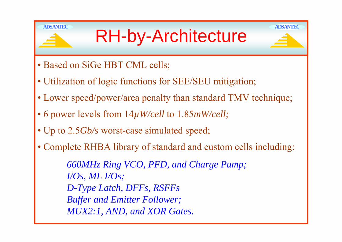
RH-by-Architecture A D S A N T E C A D S A N T E C
• Based on SiGe HBT CML cells;
• Utilization of logic functions for SEE/SEU mitigation;
• Lower speed/power/area penalty than standard TMV technique;
• 6 power levels from 14µW/cell to 1.85mW/cell;
• Up to 2.5Gb/s worst-case simulated speed;
• Complete RHBA library of standard and custom cells including:
660MHz Ring VCO, PFD, and Charge Pump;I/Os, ML I/Os;D-Type Latch, DFFs, RSFFsBuffer and Emitter Follower;MUX2:1, AND, and XOR Gates.

Strike Effects Simulations A D S A N T E C A D S A N T E C
Inputs and Outputs of Dual EF
Inputs and Outputs of a Flip-Flop
Inputs 1
Inputs 2
Outputs
Strike pulses
Outputs of the First D-Latch
Clock Input
Outputs of the Second D-Latch
SEE model includes realistic current pulses at transistor level.
Provided by J. Cressler, GeorgiaTech
Outputs of both EF and D-latch demonstrate negligible disturbance with a significant SEE-related impact at the
inputs of the circuits.
Strike pulses Strike pulses

Summary / Conclusion• A dual, low power CMOS-to-LVDS IC solution has been
presented that operates at GHz speeds with an improved level of TID protection. The IC contains switchable Data Strobingencoding/decoding circuitry that is fully Space Wire compatible and innovative I/O blocks.
• ADSANTEC has developed a novel multilevel interface (MLI) technology that significantly improves the performance of high-speed serial data links, specifically Space Wire interconnects, and has multiple fields of application.
• An innovative radiation hard by architecture (RHBA) library has been utilized to construct a ML transponder that is utilizedin the presented switch fabric intended for cPCI bus extension.
A D S A N T E C A D S A N T E C


![8PS-WG 3PS-W 3PS-WG 4pS-W 4ps-WG 0.7 2m 4m 5PS-W 5PS-WG 6PS-W 6PS-WG 7PS-W 7PS-WG 2.8 SIZE No. EJECTOR 2PS-W 2PS-WG 0.25(š (L / min) L5PS-WD±åÊ] MPaG 0m 3m 7m 10m 14m 17m 20m 0m](https://static.fdocuments.net/doc/165x107/5b037c037f8b9a2e228c75cb/8ps-wg-3ps-w-3ps-wg-4ps-w-4ps-wg-07-2m-4m-5ps-w-5ps-wg-6ps-w-6ps-wg-7ps-w-7ps-wg.jpg)