ADS1299(-4, -6) Datasheet - Texas Instruments · extracranial electroencephalogram (EEG) and...
83
Control CLK GPIO AND CONTROL Oscillator SPI Test Signals and Monitors SPI PATIENT BIAS AND REFERENCE Reference REF ADC7 ADC8 ADC1 ADC2 ADC3 ADC4 ADC5 ADC6 A7 A8 A1 A2 A3 A4 A5 A6 MUX INPUTS ¼ ¼ To Channel ADS1299 Only ADS1299-6, ADS1299 Only Product Folder Order Now Technical Documents Tools & Software Support & Community An IMPORTANT NOTICE at the end of this data sheet addresses availability, warranty, changes, use in safety-critical applications, intellectual property matters and other important disclaimers. PRODUCTION DATA. ADS1299, ADS1299-4, ADS1299-6 SBAS499C – JULY 2012 – REVISED JANUARY 2017 ADS1299-x Low-Noise, 4-, 6-, 8-Channel, 24-Bit, Analog-to-Digital Converter for EEG and Biopotential Measurements 1 1 Features 1• Up to Eight Low-Noise PGAs and Eight High- Resolution Simultaneous-Sampling ADCs • Input-Referred Noise: 1 μV PP (70-Hz BW) • Input Bias Current: 300 pA • Data Rate: 250 SPS to 16 kSPS • CMRR: –110 dB • Programmable Gain: 1, 2, 4, 6, 8, 12, or 24 • Unipolar or Bipolar Supplies: – Analog: 4.75 V to 5.25 V – Digital: 1.8 V to 3.6 V • Built-In Bias Drive Amplifier, Lead-Off Detection, Test Signals • Built-In Oscillator • Internal or External Reference • Flexible Power-Down, Standby Mode • Pin-Compatible with the ADS129x • SPI-Compatible Serial Interface • Operating Temperature Range: –40°C to +85°C 2 Applications • Medical Instrumentation Including: – Electroencephalogram (EEG) Study – Fetal Electrocardiography (ECG) – Sleep Study Monitor – Bispectral Index (BIS) – Evoked Audio Potential (EAP) 3 Description The ADS1299-4, ADS1299-6, and ADS1299 devices are a family of four-, six-, and eight-channel, low- noise, 24-bit, simultaneous-sampling delta-sigma (ΔΣ) analog-to-digital converters (ADCs) with a built-in programmable gain amplifier (PGA), internal reference, and an onboard oscillator. The ADS1299-x incorporates all commonly-required features for extracranial electroencephalogram (EEG) and electrocardiography (ECG) applications. With its high levels of integration and exceptional performance, the ADS1299-x enables the creation of scalable medical instrumentation systems at significantly reduced size, power, and overall cost. The ADS1299-x has a flexible input multiplexer per channel that can be independently connected to the internally-generated signals for test, temperature, and lead-off detection. Additionally, any configuration of input channels can be selected for derivation of the patient bias output signal. Optional SRB pins are available to route a common signal to multiple inputs for a referential montage configuration. The ADS1299-x operates at data rates from 250 SPS to 16 kSPS. Lead-off detection can be implemented internal to the device using an excitation current sink or source. Multiple ADS1299-4, ADS1299-6, or ADS1299 devices can be cascaded in high channel count systems in a daisy-chain configuration. The ADS1299-x is offered in a TQFP-64 package specified from –40°C to +85°C. Device Information (1) PART NUMBER PACKAGE BODY SIZE (NOM) ADS1299-x TQFP (64) 10.00 mm × 10.00 mm (1) For all available packages, see the orderable addendum at the end of the data sheet. Block Diagram
Transcript of ADS1299(-4, -6) Datasheet - Texas Instruments · extracranial electroencephalogram (EEG) and...

Control
CLK
GP
IOA
ND
CO
NT
RO
L
Oscillator
SPI
Test Signals andMonitors
SP
I
PATIENT BIAS AND REFERENCE
Reference
REF
ADC7
ADC8
ADC1
ADC2
ADC3
ADC4
ADC5
ADC6
A7
A8
A1
A2
A3
A4
A5
A6
MUX
INP
UT
S
¼
¼
To Channel
AD
S1299 O
nly
AD
S1299-6
,A
DS
1299 O
nly
Product
Folder
Order
Now
Technical
Documents
Tools &
Software
Support &Community
An IMPORTANT NOTICE at the end of this data sheet addresses availability, warranty, changes, use in safety-critical applications,intellectual property matters and other important disclaimers. PRODUCTION DATA.
ADS1299, ADS1299-4, ADS1299-6SBAS499C –JULY 2012–REVISED JANUARY 2017
ADS1299-x Low-Noise, 4-, 6-, 8-Channel, 24-Bit, Analog-to-Digital Converter for EEG andBiopotential Measurements
1
1 Features1• Up to Eight Low-Noise PGAs and Eight High-
Resolution Simultaneous-Sampling ADCs• Input-Referred Noise: 1 μVPP (70-Hz BW)• Input Bias Current: 300 pA• Data Rate: 250 SPS to 16 kSPS• CMRR: –110 dB• Programmable Gain: 1, 2, 4, 6, 8, 12, or 24• Unipolar or Bipolar Supplies:
– Analog: 4.75 V to 5.25 V– Digital: 1.8 V to 3.6 V
• Built-In Bias Drive Amplifier,Lead-Off Detection, Test Signals
• Built-In Oscillator• Internal or External Reference• Flexible Power-Down, Standby Mode• Pin-Compatible with the ADS129x• SPI-Compatible Serial Interface• Operating Temperature Range: –40°C to +85°C
2 Applications• Medical Instrumentation Including:
– Electroencephalogram (EEG) Study– Fetal Electrocardiography (ECG)– Sleep Study Monitor– Bispectral Index (BIS)– Evoked Audio Potential (EAP)
3 DescriptionThe ADS1299-4, ADS1299-6, and ADS1299 devicesare a family of four-, six-, and eight-channel, low-noise, 24-bit, simultaneous-sampling delta-sigma (ΔΣ)analog-to-digital converters (ADCs) with a built-inprogrammable gain amplifier (PGA), internalreference, and an onboard oscillator. The ADS1299-xincorporates all commonly-required features forextracranial electroencephalogram (EEG) andelectrocardiography (ECG) applications. With its highlevels of integration and exceptional performance, theADS1299-x enables the creation of scalable medicalinstrumentation systems at significantly reduced size,power, and overall cost.
The ADS1299-x has a flexible input multiplexer perchannel that can be independently connected to theinternally-generated signals for test, temperature, andlead-off detection. Additionally, any configuration ofinput channels can be selected for derivation of thepatient bias output signal. Optional SRB pins areavailable to route a common signal to multiple inputsfor a referential montage configuration. TheADS1299-x operates at data rates from 250 SPS to16 kSPS. Lead-off detection can be implementedinternal to the device using an excitation current sinkor source.
Multiple ADS1299-4, ADS1299-6, or ADS1299devices can be cascaded in high channel countsystems in a daisy-chain configuration. TheADS1299-x is offered in a TQFP-64 packagespecified from –40°C to +85°C.
Device Information(1)
PART NUMBER PACKAGE BODY SIZE (NOM)ADS1299-x TQFP (64) 10.00 mm × 10.00 mm
(1) For all available packages, see the orderable addendum atthe end of the data sheet.
Block Diagram

2
ADS1299, ADS1299-4, ADS1299-6SBAS499C –JULY 2012–REVISED JANUARY 2017 www.ti.com
Product Folder Links: ADS1299 ADS1299-4 ADS1299-6
Submit Documentation Feedback Copyright © 2012–2017, Texas Instruments Incorporated
Table of Contents1 Features .................................................................. 12 Applications ........................................................... 13 Description ............................................................. 14 Revision History..................................................... 25 Device Comparison ............................................... 56 Pin Configuration and Functions ......................... 57 Specifications......................................................... 7
7.1 Absolute Maximum Ratings ...................................... 77.2 ESD Ratings.............................................................. 77.3 Recommended Operating Conditions....................... 87.4 Thermal Information .................................................. 87.5 Electrical Characteristics........................................... 97.6 Timing Requirements: Serial Interface.................... 127.7 Switching Characteristics: Serial Interface.............. 127.8 Typical Characteristics ............................................ 13
8 Parametric Measurement Information ............... 168.1 Noise Measurements .............................................. 16
9 Detailed Description ............................................ 189.1 Overview ................................................................. 189.2 Functional Block Diagram ....................................... 199.3 Feature Description................................................. 209.4 Device Functional Modes........................................ 349.5 Programming........................................................... 38
9.6 Register Maps ......................................................... 4410 Applications and Implementation...................... 61
10.1 Application Information.......................................... 6110.2 Typical Application ................................................ 66
11 Power Supply Recommendations ..................... 7011.1 Power-Up Sequencing .......................................... 7011.2 Connecting the Device to Unipolar (5 V and 3.3 V)
Supplies ................................................................... 7011.3 Connecting the Device to Bipolar (±2.5 V and 3.3 V)
Supplies ................................................................... 7112 Layout................................................................... 72
12.1 Layout Guidelines ................................................. 7212.2 Layout Example .................................................... 72
13 Device and Documentation Support ................. 7413.1 Documentation Support ........................................ 7413.2 Related Links ........................................................ 7413.3 Receiving Notification of Documentation Updates 7413.4 Community Resources.......................................... 7413.5 Trademarks ........................................................... 7413.6 Electrostatic Discharge Caution............................ 7413.7 Glossary ................................................................ 74
14 Mechanical, Packaging, and OrderableInformation ........................................................... 75
4 Revision HistoryNOTE: Page numbers for previous revisions may differ from page numbers in the current version.
Changes from Revision B (October 2016) to Revision C Page
• Changed Maximum Junction parameter name to Junction in Absolute Maximum Ratings table .......................................... 7• Changed Recommended Operating Conditions table: changed free-air to ambient in conditions statement, changed
specifications of Input voltage parameter, and added VCM and fCLK symbols ........................................................................ 8• Changed conditions statement of Electrical Characteristics table: added TA to temperature conditions, moved DVDD
condition to after AVDD – AVSS condition ............................................................................................................................ 9• Changed Input bias current parameter test conditions from input to InxP and INxN ............................................................. 9• Changed Drift parameter unit from ppm to ppm/°C and changed Internal clock accuracy parameter test conditions
from –40°C ≤ TA ≤ +85°C to TA = –40°C to +85°C in Electrical Characteristics table ......................................................... 10• Changed IAVDD and IDVDD parameters [deleted (normal mode) from parameter names and added Normal mode to
test conditions], and deleted Quiescent from Power dissipation parameter name in Electrical Characteristics table ......... 11• Changed free-air to ambient in conditions statement of Timing Requirements: Serial Interface table ................................ 12• Changed Analog Input section ............................................................................................................................................ 22• Changed Table 9 cross-reference to Table 7 in Settling Time section ................................................................................ 34• Changed Ideal Output Code versus Input Signal table: changed all VREF in first column to FS in and deleted footnote
1 ........................................................................................................................................................................................... 38• Changed reset settings of bits 4 and 3 in bit register of CONFIG1 register......................................................................... 46• Changed reset value settings of bits 7 to 5 in CONFIG2 register: split cells apart .............................................................. 47• Changed reset value settings of bits 6 to 5 in CONFIG3 register: split cells apart ............................................................. 48• Changed AVDD – AVSS to AVDD + AVSS in description of bit 3 in Configuration Register 3 Field Descriptions ............. 48• Changed Lead-Off Control Register Field Descriptions table: changed 01 bit setting of bits 3:2 to 24 nA from 12 nA
changed description of bits 1:0............................................................................................................................................. 49• Changed Unused Inputs and Outputs section: added DRDY description, deleted statement of not floating unused

3
ADS1299, ADS1299-4, ADS1299-6www.ti.com SBAS499C –JULY 2012–REVISED JANUARY 2017
Product Folder Links: ADS1299 ADS1299-4 ADS1299-6
Submit Documentation FeedbackCopyright © 2012–2017, Texas Instruments Incorporated
Revision History (continued)digital inputs ......................................................................................................................................................................... 61
• Deleted second Layout Guidelines sub-section from Layout section .................................................................................. 72
Changes from Revision A (August 2012) to Revision B Page
• Added ESD Ratings table, Feature Description section, Device Functional Modes, Application and Implementationsection, Power Supply Recommendations section, Layout section, Device and Documentation Support section, andMechanical, Packaging, and Orderable Information section ................................................................................................. 1
• Added ADS1299-4 and ADS1299-6 to document .................................................................................................................. 1• Added .................................................................................................................................................................................... 1• Deleted Low Power Features bullet ...................................................................................................................................... 1• Changed extracranial electroencephalogram (EEG) in Applications and Description sections ............................................. 1• Deleted last Applications bullet .............................................................................................................................................. 1• Changed Description section: added sentence on SRB pins, changed last sentence of second paragraph ........................ 1• Changed ADS1299 family to ADS1299-x throughout document ........................................................................................... 1• Changed Block Diagram: added dotted boxes ...................................................................................................................... 1• Changed specifications for Lead-Off Detect, Frequency parameter of Electrical Characteristics table............................... 10• Added specifications for ADS1299-4 and ADS1299-6 in Supply Current (Bias Turned Off) and Power Dissipation
(Analog Supply = 5 V, Bias Amplifiers Turned Off) sections of Electrical Characteristics table .......................................... 11• Changed Noise Measurements section................................................................................................................................ 16• Changed Functional Block Diagram to show channels 5-8 not covered in ADS1299-4 and channels 7-8 not covered
in ADS1299-6 ....................................................................................................................................................................... 19• Changed INxP and INxN pins in Figure 18 ......................................................................................................................... 20• Changed Figure 23: changed PgaP, PgaN to PGAp, PGAn ............................................................................................... 23• Changed Input Common-Mode Range section: changed input common-mode range description .................................... 23• Changed differential input voltage range in the Input Differential Dynamic Range section ................................................. 24• Changed Figure 34: MUX8[2:0] = 010 on IN8N, and BIAS_MEAS = 1 on BIASIN ............................................................. 29• Changed first sentence of second paragraph in Lead-Off Detection section....................................................................... 30• Changed AC Lead-Off (One Time or Periodic) section........................................................................................................ 31• Changed Bias Lead-Off section............................................................................................................................................ 32• Changed title of Figure 38 and power-down description in Bias Drive (DC Bias Circuit) section ........................................ 33• Changed START Opcode to START in Figure 39................................................................................................................ 34• Changed Reset (RESET) section for clarity ......................................................................................................................... 35• Changed title, first paragraph, START Opcode and STOP Opcode to START and STOP (Figure 42), and STOP
Opcode to STOP Command (Figure 43) in Continuous Conversion Mode section............................................................. 36• Added last sentence to Data Input (DIN) section ................................................................................................................. 39• Added cross-reference to the Sending Multi-Byte Commands section in RDATAC: Read Data Continuous section ........ 41• Changed RDATAC Opcode to RDATAC in Figure 46.......................................................................................................... 41• Changed RDATA Opcode to RDATA in Figure 46............................................................................................................... 42• Changed description of SCLK rate restrictions, OPCODE 1 and OPCODE 2 to BYTE 1 and BYTE 2 in Figure 48 of
RREG: Read From Register section .................................................................................................................................... 43• Changed footnotes 1 and 2 and added more cross-references to footnotes in rows 0Dh to 11h in Table 11 ................... 44• Changed register description and description of bit 5 in MISC1: Miscellaneous 1 Register section ................................... 59• Changed output names in Figure 68 from RA, LA, and RL to Electrode 1, Electrode 2, and BIAS Electrode,
respectively........................................................................................................................................................................... 63• Changed Power-Up Sequencing section.............................................................................................................................. 70

4
ADS1299, ADS1299-4, ADS1299-6SBAS499C –JULY 2012–REVISED JANUARY 2017 www.ti.com
Product Folder Links: ADS1299 ADS1299-4 ADS1299-6
Submit Documentation Feedback Copyright © 2012–2017, Texas Instruments Incorporated
Changes from Original (July 2012) to Revision A Page
• Changed product column of Family and Ordering Information table ..................................................................................... 1

48
47
46
45
44
43
42
41
40
39
38
37
36
35
34
33
DVDD
GPIO4
GPIO3
GPIO2
DOUT
GPIO1
DAISY_IN
SCLK
START
CLK
DIN
DGND
DRDY
CS
RESET
PWDN
1
2
3
4
5
6
7
8
9
10
11
12
13
14
15
16
IN8N
IN8P
IN7N
IN7P
IN6N
IN6P
IN5N
IN5P
IN4N
IN4P
IN3N
IN3P
IN2N
IN2P
IN1N
IN1P
RE
SE
RV
ED
BIA
SO
UT
BIA
SIN
BIA
SIN
V
BIA
SR
EF
AV
DD
AV
SS
AV
SS
AV
DD
VC
AP
3
AV
DD
1
AV
SS
1
CLK
SE
L
DG
ND
DV
DD
DG
ND
SR
B1 2
AV
DD
AV
SS
AV
DD
AV
DD
AV
SS
VR
EF
P
VR
EF
N
VC
AP
4
NC
VC
AP
1
NC
VC
AP
2
RE
SV
1
AV
SS
SR
B
17
18
19
20
21
22
23
24
25
26
27
28
29
30
31
32
64
63
62
61
60
59
58
57
56
55
54
53
52
51
50
49
5
ADS1299, ADS1299-4, ADS1299-6www.ti.com SBAS499C –JULY 2012–REVISED JANUARY 2017
Product Folder Links: ADS1299 ADS1299-4 ADS1299-6
Submit Documentation FeedbackCopyright © 2012–2017, Texas Instruments Incorporated
5 Device Comparison
PRODUCTPACKAGEOPTIONS
OPERATINGTEMPERATURE
RANGE CHANNELS ADC RESOLUTIONMAXIMUM
SAMPLING RATEADS1299-4 TQFP-64 –40°C to +85°C 4 24 16 kSPSADS1299-6 TQFP-64 –40°C to +85°C 6 24 16 kSPSADS1299 TQFP-64 –40°C to +85°C 8 24 16 kSPS
6 Pin Configuration and Functions
PAG Package64-Pin TQFP
Top View

6
ADS1299, ADS1299-4, ADS1299-6SBAS499C –JULY 2012–REVISED JANUARY 2017 www.ti.com
Product Folder Links: ADS1299 ADS1299-4 ADS1299-6
Submit Documentation Feedback Copyright © 2012–2017, Texas Instruments Incorporated
(1) Set the two-state mode setting pins high to DVDD or low to DGND through ≥10-kΩ resistors.(2) Connect unused analog inputs directly to AVDD.
Pin FunctionsPIN
TYPE DESCRIPTIONNAME NO.
AVDD19, 21, 22, 56, 59 Supply Analog supply. Connect a 1-μF capacitor to AVSS.
59 Supply Charge pump analog supply. Connect a 1-μF capacitor to AVSS, pin 58.
AVDD1 54 Supply Analog supply. Connect a 1-μF capacitor to AVSS1.
AVSS20, 23, 32, 57 Supply Analog ground
58 Supply Analog ground for charge pump
AVSS1 53 Supply Analog ground
BIASIN 62 Analog input Bias drive input to MUX
BIASINV 61 Analog input/output Bias drive inverting input
BIASOUT 63 Analog output Bias drive output
BIASREF 60 Analog input Bias drive noninverting input
CS 39 Digital input Chip select, active low
CLK 37 Digital input Master clock input
CLKSEL 52 Digital input Master clock select (1)
DAISY_IN 41 Digital input Daisy-chain input
DGND 33, 49, 51 Supply Digital ground
DIN 34 Digital input Serial data input
DOUT 43 Digital output Serial data output
DRDY 47 Digital output Data ready, active low
DVDD 48, 50 Supply Digital power supply. Connect a 1-μF capacitor to DGND.
GPIO1 42 Digital input/output General-purpose input/output pin 1.Connect to DGND with a ≥10-kΩ resistor if unused.
GPIO2 44 Digital input/output General-purpose input/output pin 2.Connect to DGND with a ≥10-kΩ resistor if unused.
GPIO3 45 Digital input/output General-purpose input/output pin 3.Connect to DGND with a ≥10-kΩ resistor if unused.
GPIO4 46 Digital input/output General-purpose input/output pin 4.Connect to DGND with a ≥10-kΩ resistor if unused.
IN1N 15 Analog input Differential analog negative input 1 (2)
IN1P 16 Analog input Differential analog positive input 1 (2)
IN2N 13 Analog input Differential analog negative input 2 (2)
IN2P 14 Analog input Differential analog positive input 2 (2)
IN3N 11 Analog input Differential analog negative input 3 (2)
IN3P 12 Analog input Differential analog positive input 3 (2)
IN4N 9 Analog input Differential analog negative input 4 (2)
IN4P 10 Analog input Differential analog positive input 4 (2)
IN5N 7 Analog input Differential analog negative input 5 (2) (ADS1299-6 and ADS1299 only)
IN5P 8 Analog input Differential analog positive input 5 (2) (ADS1299-6 and ADS1299 only)
IN6N 5 Analog input Differential analog negative input 6 (2) (ADS1299-6 and ADS1299 only)
IN6P 6 Analog input Differential analog positive input 6 (2) (ADS1299-6 and ADS1299 only)
IN7N 3 Analog input Differential analog negative input 7 (2) (ADS1299 only)
IN7P 4 Analog input Differential analog positive input 7 (2) (ADS1299 only)
IN8N 1 Analog input Differential analog negative input 8 (2) (ADS1299 only)
IN8P 2 Analog input Differential analog positive input 8 (2) (ADS1299 only)
NC 27, 29 — No connection, leave as open circuit
Reserved 64 Analog output Reserved for future use, leave as open circuit
RESET 36 Digital input System reset, active low
RESV1 31 Digital input Reserved for future use, connect directly to DGND
SCLK 40 Digital input Serial clock input
SRB1 17 Analog input/output Patient stimulus, reference, and bias signal 1
SRB2 18 Analog input/output Patient stimulus, reference, and bias signal 2

7
ADS1299, ADS1299-4, ADS1299-6www.ti.com SBAS499C –JULY 2012–REVISED JANUARY 2017
Product Folder Links: ADS1299 ADS1299-4 ADS1299-6
Submit Documentation FeedbackCopyright © 2012–2017, Texas Instruments Incorporated
Pin Functions (continued)PIN
TYPE DESCRIPTIONNAME NO.
START 38 Digital input Synchronization signal to start or restart a conversion
PWDN 35 Digital input Power-down, active low
VCAP1 28 Analog output Analog bypass capacitor pin. Connect a 100-μF capacitor to AVSS.
VCAP2 30 Analog output Analog bypass capacitor pin. Connect a 1-μF capacitor to AVSS.
VCAP3 55 Analog output Analog bypass capacitor pin. Connect a parallel combination of 1-μF and 0.1-μFcapacitors to AVSS.
VCAP4 26 Analog output Analog bypass capacitor pin. Connect a 1-μF capacitor to AVSS.
VREFN 25 Analog input Negative analog reference voltage.
VREFP 24 Analog input/output Positive analog reference voltage. Connect a minimum 10-μF capacitor to VREFN.
(1) Stresses beyond those listed under Absolute Maximum Ratings may cause permanent damage to the device. These are stress ratingsonly, which do not imply functional operation of the device at these or any other conditions beyond those indicated under RecommendedOperating Conditions. Exposure to absolute-maximum-rated conditions for extended periods may affect device reliability.
(2) Input pins are diode-clamped to the power-supply rails. Limit the input current to 10 mA or less if the analog input voltage exceedsAVDD + 0.3 V or is less than AVSS – 0.3 V, or if the digital input voltage exceeds DVDD + 0.3 V or is less than DGND – 0.3 V.
7 Specifications
7.1 Absolute Maximum Ratings (1)
MIN MAX UNIT
Voltage
AVDD to AVSS –0.3 5.5
V
DVDD to DGND –0.3 3.9AVSS to DGND –3 0.2VREFP to AVSS –0.3 AVDD + 0.3VREFN to AVSS –0.3 AVDD + 0.3Analog input AVSS – 0.3 AVDD + 0.3Digital input DGND – 0.3 DVDD + 0.3
Current Input, continuous, any pin except power supply pins (2) –10 10 mA
TemperatureJunction, TJ 150
°CStorage, Tstg –60 150
(1) JEDEC document JEP155 states that 500-V HBM allows safe manufacturing with a standard ESD control process.(2) JEDEC document JEP157 states that 250-V CDM allows safe manufacturing with a standard ESD control process.
7.2 ESD RatingsVALUE UNIT
V(ESD) Electrostatic dischargeHuman-body model (HBM), per ANSI/ESDA/JEDEC JS-001 (1) ±1000
VCharged-device model (CDM), per JEDEC specification JESD22-C101 (2) ±500

8
ADS1299, ADS1299-4, ADS1299-6SBAS499C –JULY 2012–REVISED JANUARY 2017 www.ti.com
Product Folder Links: ADS1299 ADS1299-4 ADS1299-6
Submit Documentation Feedback Copyright © 2012–2017, Texas Instruments Incorporated
7.3 Recommended Operating Conditionsover operating ambient temperature range (unless otherwise noted)
MIN NOM MAX UNITPOWER SUPPLY
Analog power supply AVDD to AVSS 4.75 5 5.25 VDigital power supply DVDD to DGND 1.8 1.8 3.6 VAnalog to Digital supply AVDD – DVDD –2.1 3.6 V
ANALOG INPUTSFull-scale differential inputvoltage VINxP – VINxN ±VREF / gain V
VCM Input common-mode range (VINxP + VINxN) / 2See the Input Common-Mode Range
subsection of the PGA Settings and InputRange section
VOLTAGE REFERENCE INPUTSVREF Reference input voltage VREF = (VVREFP – VVREFN) 4.5 VVREFN Negative input AVSS VVREFP Positive input AVSS + 4.5 VCLOCK INPUTfCLK External clock input frequency CLKSEL pin = 0 1.5 2.048 2.25 MHzDIGITAL INPUTS
Input voltage DGND – 0.1 DVDD + 0.1 VTEMPERATURE RANGETA Operating temperature range –40 85 °C
(1) For more information about traditional and new thermal metrics, see the Semiconductor and IC Package Thermal Metrics applicationreport.
7.4 Thermal Information
THERMAL METRIC (1)ADS1299-4, ADS1299-6, ADS1299
UNITPAG (TQFP)64 PINS
RθJA Junction-to-ambient thermal resistance 46.2 °C/WRθJC(top) Junction-to-case (top) thermal resistance 5.8 °C/WRθJB Junction-to-board thermal resistance 19.6 °C/WψJT Junction-to-top characterization parameter 0.2 °C/WψJB Junction-to-board characterization parameter 19.2 °C/WRθJC(bot) Junction-to-case (bottom) thermal resistance n/a °C/W
9
ADS1299, ADS1299-4, ADS1299-6www.ti.com SBAS499C –JULY 2012–REVISED JANUARY 2017
Product Folder Links: ADS1299 ADS1299-4 ADS1299-6
Submit Documentation FeedbackCopyright © 2012–2017, Texas Instruments Incorporated
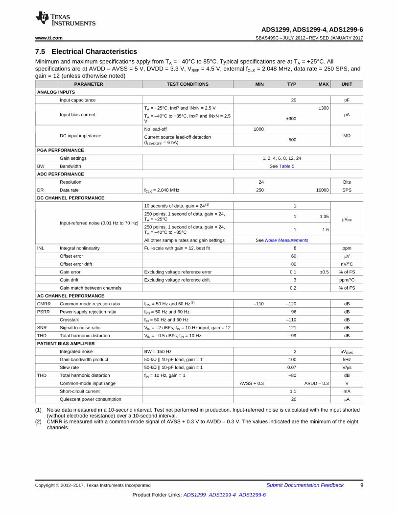
(1) Noise data measured in a 10-second interval. Test not performed in production. Input-referred noise is calculated with the input shorted(without electrode resistance) over a 10-second interval.
(2) CMRR is measured with a common-mode signal of AVSS + 0.3 V to AVDD – 0.3 V. The values indicated are the minimum of the eightchannels.
7.5 Electrical CharacteristicsMinimum and maximum specifications apply from TA = –40°C to 85°C. Typical specifications are at TA = +25°C. Allspecifications are at AVDD – AVSS = 5 V, DVDD = 3.3 V, VREF = 4.5 V, external fCLK = 2.048 MHz, data rate = 250 SPS, andgain = 12 (unless otherwise noted)
PARAMETER TEST CONDITIONS MIN TYP MAX UNIT
ANALOG INPUTS
Input capacitance 20 pF
Input bias currentTA = +25°C, InxP and INxN = 2.5 V ±300
pATA = –40°C to +85°C, InxP and INxN = 2.5V ±300
DC input impedanceNo lead-off 1000
MΩCurrent source lead-off detection(ILEADOFF = 6 nA) 500
PGA PERFORMANCE
Gain settings 1, 2, 4, 6, 8, 12, 24
BW Bandwidth See Table 5
ADC PERFORMANCE
Resolution 24 Bits
DR Data rate fCLK = 2.048 MHz 250 16000 SPS
DC CHANNEL PERFORMANCE
Input-referred noise (0.01 Hz to 70 Hz)
10 seconds of data, gain = 24 (1) 1
μVPP
250 points, 1 second of data, gain = 24,TA = +25°C 1 1.35
250 points, 1 second of data, gain = 24,TA = –40°C to +85°C 1 1.6
All other sample rates and gain settings See Noise Measurements
INL Integral nonlinearity Full-scale with gain = 12, best fit 8 ppm
Offset error 60 μV
Offset error drift 80 nV/°C
Gain error Excluding voltage reference error 0.1 ±0.5 % of FS
Gain drift Excluding voltage reference drift 3 ppm/°C
Gain match between channels 0.2 % of FS
AC CHANNEL PERFORMANCE
CMRR Common-mode rejection ratio fCM = 50 Hz and 60 Hz (2) –110 –120 dB
PSRR Power-supply rejection ratio fPS = 50 Hz and 60 Hz 96 dB
Crosstalk fIN = 50 Hz and 60 Hz –110 dB
SNR Signal-to-noise ratio VIN = –2 dBFs, fIN = 10-Hz input, gain = 12 121 dB
THD Total harmonic distortion VIN = –0.5 dBFs, fIN = 10 Hz –99 dB
PATIENT BIAS AMPLIFIER
Integrated noise BW = 150 Hz 2 μVRMS
Gain bandwidth product 50-kΩ || 10-pF load, gain = 1 100 kHz
Slew rate 50-kΩ || 10-pF load, gain = 1 0.07 V/μs
THD Total harmonic distortion fIN = 10 Hz, gain = 1 –80 dB
Common-mode input range AVSS + 0.3 AVDD – 0.3 V
Short-circuit current 1.1 mA
Quiescent power consumption 20 μA

10
ADS1299, ADS1299-4, ADS1299-6SBAS499C –JULY 2012–REVISED JANUARY 2017 www.ti.com
Product Folder Links: ADS1299 ADS1299-4 ADS1299-6
Submit Documentation Feedback Copyright © 2012–2017, Texas Instruments Incorporated
Electrical Characteristics (continued)Minimum and maximum specifications apply from TA = –40°C to 85°C. Typical specifications are at TA = +25°C. Allspecifications are at AVDD – AVSS = 5 V, DVDD = 3.3 V, VREF = 4.5 V, external fCLK = 2.048 MHz, data rate = 250 SPS, andgain = 12 (unless otherwise noted)
PARAMETER TEST CONDITIONS MIN TYP MAX UNIT
LEAD-OFF DETECT
FrequencyContinuous At dc, fDR / 4,
see Register Maps for settings HzOne time or periodic 7.8, 31.2
Current
ILEAD_OFF[1:0] = 00 6nA
ILEAD_OFF[1:0] = 01 24
ILEAD_OFF[1:0] = 10 6μA
ILEAD_OFF[1:0] = 11 24
Current accuracy ±20%
Comparator threshold accuracy ±30 mV
EXTERNAL REFERENCE
Input impedance 5.6 kΩ
INTERNAL REFERENCE
VREF Internal reference voltage 4.5 V
VREF accuracy ±0.2%
Drift TA = –40°C to +85°C 35 ppm/°C
Start-up time 150 ms
SYSTEM MONITORS
Reading errorAnalog supply 2%
Digital supply 2%
Device wake upFrom power-up to DRDY low 150 ms
STANDBY mode 31.25 µs
Temperaturesensor reading
Voltage TA = +25°C 145 mV
Coefficient 490 μV/°C
Test signal
Signal frequency See Register Maps section for settings fCLK / 221, fCLK / 220 Hz
Signal voltage See Register Maps section for settings ±1, ±2 mV
Accuracy ±2%
CLOCK
Internal oscillator clock frequency Nominal frequency 2.048 MHz
Internal clock accuracyTA = +25°C ±0.5%
TA = –40°C to +85°C ±2.5%
Internal oscillator start-up time 20 μs
Internal oscillator power consumption 120 μW
DIGITAL INPUT/OUTPUT (DVDD = 1.8 V to 3.6 V)
VIH High-level input voltage 0.8 DVDD DVDD + 0.1 V
VIL Low-level input voltage –0.1 0.2 DVDD V
VOH High-level output voltage IOH = –500 μA 0.9 DVDD V
VOL Low-level output voltage IOL = +500 μA 0.1 DVDD V
Input current 0 V < VDigitalInput < DVDD –10 10 μA

11
ADS1299, ADS1299-4, ADS1299-6www.ti.com SBAS499C –JULY 2012–REVISED JANUARY 2017
Product Folder Links: ADS1299 ADS1299-4 ADS1299-6
Submit Documentation FeedbackCopyright © 2012–2017, Texas Instruments Incorporated
Electrical Characteristics (continued)Minimum and maximum specifications apply from TA = –40°C to 85°C. Typical specifications are at TA = +25°C. Allspecifications are at AVDD – AVSS = 5 V, DVDD = 3.3 V, VREF = 4.5 V, external fCLK = 2.048 MHz, data rate = 250 SPS, andgain = 12 (unless otherwise noted)
PARAMETER TEST CONDITIONS MIN TYP MAX UNIT
SUPPLY CURRENT (Bias Turned Off)
IAVDD AVDD current
ADS1299-4
Normal mode, AVDD – AVSS = 5 V
4.06
mAADS1299-6 5.57
ADS1299 7.14
IDVDD DVDD current
ADS1299-4
Normal mode, DVDD = 3.3 V
0.54
mA
ADS1299-6 0.66
ADS1299 1
ADS1299-4
Normal mode, DVDD = 1.8 V
0.27
ADS1299-6 0.34
ADS1299 0.5
POWER DISSIPATION (Analog Supply = 5 V, Bias Amplifiers Turned Off)
Power dissipation
ADS1299-4
Normal mode 22 24 mW
Power-down 10 µW
Standby mode, internal reference 5.1 mW
ADS1299-6
Normal mode 30 33 mW
Power-down 10 µW
Standby mode, internal reference 5.1 mW
ADS1299
Normal mode 39 42 mW
Power-down 10 µW
Standby mode, internal reference 5.1 mW

D ISY_INA
DOUT
SCLK
MSBD1
tDISCK2ST
MSB
21 3 216 217 218
MSBD1LSB
tDISCK2HT
LSBD1
219
1
CS
SCLK
DIN
DOUT
2 3 8 1 2 83
tCSSC
tDIST
tDIHD
tDOHD
tCSH
tDOPD
tSPWH
tSPWL
tSCCS
Hi-Z
tCSDOZt
CSDOD
Hi-Z
tSCLK
tSDECODE
CLK
tCLK
12
ADS1299, ADS1299-4, ADS1299-6SBAS499C –JULY 2012–REVISED JANUARY 2017 www.ti.com
Product Folder Links: ADS1299 ADS1299-4 ADS1299-6
Submit Documentation Feedback Copyright © 2012–2017, Texas Instruments Incorporated
7.6 Timing Requirements: Serial Interfaceover operating ambient temperature range (unless otherwise noted)
2.7 V ≤ DVDD ≤ 3.6 V 1.8 V ≤ DVDD ≤ 2.0 VUNITMIN MAX MIN MAX
tCLK Master clock period 414 666 414 666 nstCSSC Delay time, CS low to first SCLK 6 17 nstSCLK SCLK period 50 66.6 nstSPWH, L Pulse duration, SCLK pulse duration, high or low 15 25 nstDIST Setup time, DIN valid to SCLK falling edge 10 10 nstDIHD Hold time, valid DIN after SCLK falling edge 10 11 nstCSH Pulse duration, CS high 2 2 tCLK
tSCCS Delay time, final SCLK falling edge to CS high 4 4 tCLK
tSDECODE Command decode time 4 4 tCLK
tDISCK2ST Setup time, DAISY_IN valid to SCLK rising edge 10 10 nstDISCK2HT Hold time, DAISY_IN valid after SCLK rising edge 10 10 ns
7.7 Switching Characteristics: Serial Interfaceover operating ambient temperature range (unless otherwise noted)
PARAMETER2.7 V ≤ DVDD ≤ 3.6 V 1.8 V ≤ DVDD ≤ 2.0 V
UNITMIN MAX MIN MAXtDOHD Hold time, SCLK falling edge to invalid DOUT 10 10 nstDOPD Propagation delay time, SCLK rising edge to DOUT valid 17 32 nstCSDOD Propagation delay time, CS low to DOUT driven 10 20 nstCSDOZ Propagation delay time, CS high to DOUT Hi-Z 10 20 ns
NOTE: SPI settings are CPOL = 0 and CPHA = 1.
Figure 1. Serial Interface Timing
Figure 2. Daisy-Chain Interface Timing

0
25
50
75
100
125
150
175
200
−40 −30 −20 −10 0 10 20 30 40 50 60 70 80 90Temperature (°C)
Leak
age
Cur
rent
(pA
)
Input Voltage = 2.5 VData Rate = 250 SPS to 8 kSPS
G007
80
85
90
95
100
105
110
115
120
10 100 1000Frequency (Hz)
Pow
er−
Sup
ply
Rej
ectio
n R
atio
(dB
) G = 1G = 2 G = 4
G = 6G = 8G = 12
G = 24
G008
−135
−130
−125
−120
−115
−110
−105
−100
10 100 1000Frequency (Hz)
CM
RR
(dB
)
Gain = 1Gain = 2Gain = 4Gain = 6Gain = 8Gain = 12Gain = 24
Data Rate = 4 kSPSAIN = AVDD − 0.3 V to AVSS + 0.3 V
G005
0
50
100
150
200
250
300
350
400
0 0.5 1 1.5 2 2.5 3 3.5 4 4.5 5Input Voltage (V)
Inpu
t Lea
kage
Cur
rent
(pA
)Data Rate = 250 SPS to 8 kSPS Data Rate = 16 kSPS
G006
−0.
5
−0.
4
−0.
3
−0.
2
−0.
1 0
0.1
0.2
0.3
0.4
0.5
−0.
5
−0.
4
−0.
3
−0.
2
−0.
1 0
0.1
0.2
0.3
0.4
0.5
0
100
200
300
400
500
600
700
800
Input−Referred Noise (µV)
Occ
uren
ces
Gain = 24
G004
−0.5
−0.4
−0.3
−0.2
−0.1
0
0.1
0.2
0.3
0.4
0.5
1 2 3 4 5 6 7 8 9 10Time (s)
Inpu
t−R
efer
red
Noi
se (
µV)
Gain = 24
G003
13
ADS1299, ADS1299-4, ADS1299-6www.ti.com SBAS499C –JULY 2012–REVISED JANUARY 2017
Product Folder Links: ADS1299 ADS1299-4 ADS1299-6
Submit Documentation FeedbackCopyright © 2012–2017, Texas Instruments Incorporated
7.8 Typical CharacteristicsAt TA = 25°C, AVDD = 5 V, AVSS = 0 V, DVDD = 3.3 V, internal VREFP = 4.5 V, VREFN = AVSS, external clock = 2.048MHz, data rate = 250 SPS, and gain = 12 (unless otherwise noted)
Figure 3. Input-Referred Noise Figure 4. Noise Histogram
Figure 5. Common-Mode Rejection Ratio vs Frequency Figure 6. Leakage Current vs Input Voltage
Figure 7. Leakage Current vs Temperature Figure 8. PSRR vs Frequency

−180
−160
−140
−120
−100
−80
−60
−40
−20
0
0 2000 4000 6000 8000Frequency (Hz)
Am
plitu
de (
dBF
S)
PGA Gain = 12THD = −94 dBSNR = 101 dBData Rate = 16 kSPS
G013
0
100
200
300
400
500
600
1 10 30PGA Gain
Offs
et (
µV)
G014
−10
−8
−6
−4
−2
0
2
4
6
8
−1 −0.8 −0.6 −0.4 −0.2 0 0.2 0.4 0.6 0.8 1Input Range (Normalized to Full−Scale)
Inte
gral
Non
linea
rity
(pp
m)
+25°C−40°C+85°C
Gain = 12
G011
−180
−160
−140
−120
−100
−80
−60
−40
−20
0
0 50 100 150 200 250Frequency (Hz)
Am
plitu
de (
dBF
S)
PGA Gain = 12THD = −99 dBSNR = 120 dBData Rate = 500 SPS
G012
−105
−100
−95
−90
−85
−80
−75
−70
−65
−60
10 100 1000Frequency (Hz)
Tot
al H
arm
onic
Dis
tort
ion
(dB
)
Gain = 1 Gain = 2Gain = 4Gain = 6Gain = 8Gain = 12Gain = 24
Data Rate = 8 kSPSAIN = −0.5 dBFS
G009
−10
−8
−6
−4
−2
0
2
4
6
8
10
12
−1 −0.8 −0.6 −0.4 −0.2 0 0.2 0.4 0.6 0.8 1Input (Normalized to Full-Scale)
Inte
gral
Non
linea
rity
(ppm
)
Gain = 1Gain = 2Gain = 4Gain = 6Gain = 8Gain = 12Gain = 24
G010
14
ADS1299, ADS1299-4, ADS1299-6SBAS499C –JULY 2012–REVISED JANUARY 2017 www.ti.com
Product Folder Links: ADS1299 ADS1299-4 ADS1299-6
Submit Documentation Feedback Copyright © 2012–2017, Texas Instruments Incorporated
Typical Characteristics (continued)At TA = 25°C, AVDD = 5 V, AVSS = 0 V, DVDD = 3.3 V, internal VREFP = 4.5 V, VREFN = AVSS, external clock = 2.048MHz, data rate = 250 SPS, and gain = 12 (unless otherwise noted)
Figure 9. THD vs Frequency Figure 10. INL vs PGA Gain
Figure 11. INL vs Temperature Figure 12. THD FFT Plot (60-Hz Signal)
Figure 13. FFT Plot (60-Hz Signal) Figure 14. Offset vs PGA Gain (Absolute Value)

−3.
5
−3
−2.
5
−2
−1.
5
−1
−0.
5 0
0.5 1
1.5 2
2.5
−3.
5
−3
−2.
5
−2
−1.
5
−1
−0.
5 0
0.5 1
1.5 2
2.5
0
50
100
150
200
250
300
350
Error in Current Magnitude (nA)
Num
ber
of B
ins
Current Setting = 24 nA
G017
80
70
60
50
40
30
20
10
0
-20
Threshold Error (mV)
Num
ber
of B
ins
-15 0
10
20
30
35
25
155
-10
Data From 31 Devices, Two Lots
G016
70
60
50
40
30
20
10
0
-0
.53
Error (%)
Nu
mb
er
of
Bin
s
-0
.41
-0
.18
0.0
6
0.3
0.5
4
0.6
6
0.4
2
0.1
8
-0
.06
-0
.29
Data From 31 Devices, Two Lots
G015
15
ADS1299, ADS1299-4, ADS1299-6www.ti.com SBAS499C –JULY 2012–REVISED JANUARY 2017
Product Folder Links: ADS1299 ADS1299-4 ADS1299-6
Submit Documentation FeedbackCopyright © 2012–2017, Texas Instruments Incorporated
Typical Characteristics (continued)At TA = 25°C, AVDD = 5 V, AVSS = 0 V, DVDD = 3.3 V, internal VREFP = 4.5 V, VREFN = AVSS, external clock = 2.048MHz, data rate = 250 SPS, and gain = 12 (unless otherwise noted)
Figure 15. Test Signal Amplitude Accuracy Figure 16. Lead-Off Comparator Threshold Accuracy
Figure 17. Lead-Off Current Source Accuracy Distribution

RMS
VREFDynamic Range = 20 log
2 Gain V
§ ·u ¨ ¸¨ ¸u u© ¹
2RMS
VREFENOB = log
2 Gain V
§ ·¨ ¸¨ ¸u u© ¹
16
ADS1299, ADS1299-4, ADS1299-6SBAS499C –JULY 2012–REVISED JANUARY 2017 www.ti.com
Product Folder Links: ADS1299 ADS1299-4 ADS1299-6
Submit Documentation Feedback Copyright © 2012–2017, Texas Instruments Incorporated
(1) At least 1000 consecutive readings were used to calculate the RMS and peak-to-peak noise values in this table.
8 Parametric Measurement Information
8.1 Noise Measurements
NOTEUnless otherwise noted, ADS1299-x refers to all specifications and functional descriptionsof the ADS1299-4, ADS1299-6, and ADS1299.
Optimize the ADS1299-x noise performance by adjusting the data rate and PGA setting. Reduce the data rate toincrease the averaging, and the noise drops correspondingly. Increase the PGA value to reduce the input-referred noise. This lowered noise level is particularly useful when measuring low-level biopotential signals.Table 1 to Table 4 summarize the ADS1299-x noise performance with a 5-V analog power supply. The data arerepresentative of typical noise performance at TA = +25°C. The data shown are the result of averaging thereadings from multiple devices and are measured with the inputs shorted together. A minimum of 1000consecutive readings are used to calculate the RMS and peak-to-peak noise for each reading. For the lower datarates, the ratio is approximately 6.6.
Table 1 shows measurements taken with an internal reference. The data are also representative of theADS1299-x noise performance when using a low-noise external reference such as the REF5045.
Table 1, Table 2, Table 3, and Table 4 list the input-referred noise in units of μVRMS and μVPP for the conditionsshown. The corresponding data in units of effective number of bits (ENOB) where ENOB for the RMS noise isdefined as in Equation 1:
(1)
Noise-free bits for the peak-to-peak noise are calculated with the same method.
The dynamic range data in Table 1, Table 2, Table 3, and Table 4 are calculated using Equation 2:
(2)
Table 1. Input-Referred Noise (μVRMS, μVPP) in Normal Mode5-V Analog Supply and 4.5-V Reference (1)
DR BITS OFCONFIG1
REGISTER
OUTPUTDATA RATE
(SPS)–3-dB
BANDWIDTH (Hz)
PGAGAIN = 1
PGAGAIN = 2
μVRMS μVPP
DYNAMICRANGE
(dB)
NOISE-FREEBITS ENOB μVRMS μVPP
DYNAMICRANGE
(dB)
NOISE-FREEBITS ENOB
000 16000 4193 21.70 151.89 103.3 15.85 17.16 10.85 75.94 103.3 15.85 17.16
001 8000 2096 6.93 48.53 113.2 17.50 18.81 3.65 25.52 112.8 17.43 18.74
010 4000 1048 4.33 30.34 117.3 18.18 19.49 2.28 15.95 116.9 18.11 19.41
011 2000 524 3.06 21.45 120.3 18.68 19.99 1.61 11.29 119.9 18.60 19.91
100 1000 262 2.17 15.17 123.3 19.18 20.49 1.14 7.98 122.9 19.10 20.41
101 500 131 1.53 10.73 126.3 19.68 20.99 0.81 5.65 125.9 19.60 20.91
110 250 65 1.08 7.59 129.3 20.18 21.48 0.57 3.99 128.9 20.10 21.41
111 n/a n/a — — — — — — — — — —

17
ADS1299, ADS1299-4, ADS1299-6www.ti.com SBAS499C –JULY 2012–REVISED JANUARY 2017
Product Folder Links: ADS1299 ADS1299-4 ADS1299-6
Submit Documentation FeedbackCopyright © 2012–2017, Texas Instruments Incorporated
(1) At least 1000 consecutive readings were used to calculate the RMS and peak-to-peak noise values in this table.
Table 2. Input-Referred Noise (μVRMS, μVPP) in Normal Mode5-V Analog Supply and 4.5-V Reference (1)
DR BITS OFCONFIG1
REGISTER
OUTPUTDATA RATE
(SPS)–3-dB
BANDWIDTH (Hz)
PGAGAIN = 4
PGAGAIN = 6
μVRMS μVPP
DYNAMICRANGE
(dB)
NOISE-FREEBITS ENOB μVRMS μVPP
DYNAMICRANGE
(dB)
NOISE-FREEBITS ENOB
000 16000 4193 5.60 39.23 103.0 15.81 17.12 3.87 27.10 102.7 15.76 17.06
001 8000 2096 1.98 13.87 112.1 17.31 18.62 1.31 9.19 112.1 17.32 18.62
010 4000 1048 1.24 8.66 116.1 17.99 19.29 0.93 6.50 115.1 17.82 19.12
011 2000 524 0.88 6.13 119.2 18.49 19.79 0.66 4.60 118.1 18.32 19.62
100 1000 262 0.62 4.34 122.2 18.99 20.29 0.46 3.25 121.1 18.81 20.12
101 500 131 0.44 3.07 125.2 19.49 20.79 0.33 2.30 124.1 19.31 20.62
110 250 65 0.31 2.16 128.2 19.99 21.30 0.23 1.62 127.2 19.82 21.13
111 n/a n/a — — — — — — — — — —
(1) At least 1000 consecutive readings were used to calculate the RMS and peak-to-peak noise values in this table.
Table 3. Input-Referred Noise (μVRMS, μVPP) in Normal Mode5-V Analog Supply and 4.5-V Reference (1)
DR BITS OFCONFIG1
REGISTER
OUTPUTDATA RATE
(SPS)–3-dB
BANDWIDTH (Hz)
PGAGAIN = 8
PGAGAIN = 12
μVRMS μVPP
DYNAMICRANGE
(dB)
NOISE-FREEBITS ENOB μVRMS μVPP
DYNAMICRANGE
(dB)
NOISE-FREEBITS ENOB
000 16000 4193 3.05 21.32 102.3 15.69 16.99 2.27 15.89 101.3 15.53 16.83
001 8000 2096 1.11 7.80 111.0 17.14 18.45 0.92 6.41 109.2 16.84 18.14
010 4000 1048 0.79 5.52 114.0 17.64 18.95 0.65 4.53 112.2 17.34 18.64
011 2000 524 0.56 3.90 117.1 18.14 19.44 0.46 3.20 115.2 17.84 19.14
100 1000 262 0.39 2.76 120.1 18.64 19.94 0.32 2.26 118.3 18.34 19.65
101 500 131 0.28 1.95 123.1 19.14 20.44 0.23 1.61 121.2 18.83 20.14
110 250 65 0.20 1.38 126.1 19.64 20.95 0.16 1.13 124.3 19.34 20.65
111 n/a n/a — — — — — — — — — —
(1) At least 1000 consecutive readings were used to calculate the RMS and peak-to-peak noise values in this table.
Table 4. Input-Referred Noise (μVRMS, μVPP) in Normal Mode5-V Analog Supply and 4.5-V Reference (1)
DR BITS OF CONFIG1REGISTER
OUTPUT DATARATE (SPS) –3-dB BANDWIDTH (Hz)
PGAGAIN = 24
μVRMS μVPP
DYNAMICRANGE (dB)
NOISE-FREEBITS ENOB
000 16000 4193 1.66 11.64 98.0 14.98 16.28
001 8000 2096 0.80 5.57 104.4 16.04 17.35
010 4000 1048 0.56 3.94 107.4 16.54 17.84
011 2000 524 0.40 2.79 110.4 17.04 18.35
100 1000 262 0.28 1.97 113.5 17.54 18.85
101 500 131 0.20 1.39 116.5 18.04 19.35
110 250 65 0.14 0.98 119.5 18.54 19.85
111 n/a n/a — — — — —

18
ADS1299, ADS1299-4, ADS1299-6SBAS499C –JULY 2012–REVISED JANUARY 2017 www.ti.com
Product Folder Links: ADS1299 ADS1299-4 ADS1299-6
Submit Documentation Feedback Copyright © 2012–2017, Texas Instruments Incorporated
9 Detailed Description
9.1 OverviewThe ADS1299-x is a low-noise, low-power, multichannel, simultaneously-sampling, 24-bit, delta-sigma (ΔΣ)analog-to-digital converter (ADC) with an integrated programmable gain amplifier (PGA). These devices integratevarious EEG-specific functions that makes the family well-suited for scalable electrocardiogram (ECG),electroencephalography (EEG) applications. These devices can also be used in high-performance, multichannel,data acquisition systems by powering down the ECG or EEG-specific circuitry.
The devices have a highly-programmable multiplexer that allows for temperature, supply, input short, and biasmeasurements. Additionally, the multiplexer allows any input electrodes to be programmed as the patientreference drive. The PGA gain can be chosen from one of seven settings (1, 2, 4, 6, 8, 12, and 24). The ADCs inthe device offer data rates from 250 SPS to 16 kSPS. Communication to the device is accomplished using anSPI-compatible interface. The device provides four general-purpose input/output (GPIO) pins for general use.Multiple devices can be synchronized using the START pin.
The internal reference generates a low noise 4.5 V internal voltage when enabled and the internal oscillatorgenerates a 2.048-MHz clock when enabled. The versatile patient bias drive block allows the average of anyelectrode combination to be chosen in order to generate the patient drive signal. Lead-off detection can beaccomplished by using a current source or sink. A one-time, in-band, lead-off option and a continuous, out-of-band, internal lead-off option are available.

DRDY
CLK
CLKSEL
START
MUX Oscillator
Power-Supply Signal
SPI
DVDD
DGNDBIASINV
BIASOUT
BIASREF
Lead-Off Excitation Source
GPIO1
GPIO4
GPIO3
CSSCLKDINDOUT
GPIO2
IN8P
IN8N
IN7P
IN7N
IN6P
IN6N
IN5P
IN5N
IN4P
IN4N
IN3P
IN3N
IN2P
IN2N
IN1P
IN1N
Low-NoisePGA1
DS
ADC1
Temperature Sensor Input
BIASAmplifier
Reference
VREFP VREFN
Control
PWDN
RESET
DS
ADC2
DS
ADC3
DS
ADC4
DS
ADC5
DS
ADC6
DS
ADC7
DS
ADC8
AVDD AVDD1
AVSS AVSS1
Test Signal
BIA
SIN
SR
B2
SR
B1
Low-NoisePGA8
Low-NoisePGA7
Low-NoisePGA6
Low-NoisePGA5
Low-NoisePGA4
Low-NoisePGA3
Low-NoisePGA2
AD
S1
29
9-6
an
dA
DS
12
99
On
lyA
DS
12
99
On
ly
19
ADS1299, ADS1299-4, ADS1299-6www.ti.com SBAS499C –JULY 2012–REVISED JANUARY 2017
Product Folder Links: ADS1299 ADS1299-4 ADS1299-6
Submit Documentation FeedbackCopyright © 2012–2017, Texas Instruments Incorporated
9.2 Functional Block Diagram
MUX[2:0] = 101
TempPMUX[2:0] = 100
MVDDPMUX[2:0] = 011
From LOFFP
MAIN(1)
MUX[2:0] = 110
MUX[2:0] = 001
To PGAP
To PGANMUX[2:0] = 001
MUX[2:0] = 111
INxP
INxNMAIN(1) AND SRB1
From LoffN
(AVDD+AVSS)2
MVDDN
TempN
TI DeviceMUX
INT_TEST
(VREFP + VREFN)
2
TESTP
INT_TESTTESTM
SRB2 BIAS_IN
To Next Channels
CHxSET[3] = 1
SRB1
To Next Channels
MAIN(1)
AND SRB1
MUX[2:0] = 010 ANDBIAS_MEAS
MUX[2:0] = 010AND
BIAS_MEAS
BIASREF_INT=1
BIASREF_INT=0
MUX[2:0] = 100
MUX[2:0] = 011
MUX[2:0] = 101
BIASREF
Copyright © 2016, Texas Instruments Incorporated
20
ADS1299, ADS1299-4, ADS1299-6SBAS499C –JULY 2012–REVISED JANUARY 2017 www.ti.com
Product Folder Links: ADS1299 ADS1299-4 ADS1299-6
Submit Documentation Feedback Copyright © 2012–2017, Texas Instruments Incorporated
9.3 Feature DescriptionThis section contains details of the ADS1299-x internal functional elements. The analog blocks are discussedfirst, followed by the digital interface. Blocks implementing EEG-specific functions are covered at the end of thissection.
Throughout this document, fCLK denotes the CLK pin signal frequency, tCLK denotes the CLK pin signal period,fDR denotes the output data rate, tDR denotes the output data time period, and fMOD denotes the frequency atwhich the modulator samples the input.
9.3.1 Analog Functionality
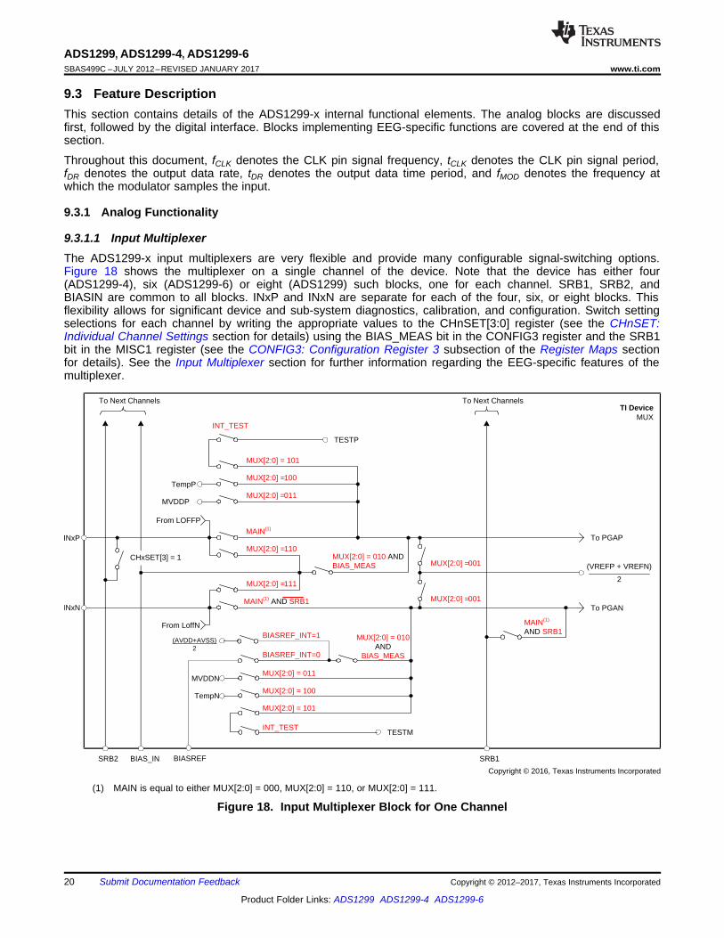
9.3.1.1 Input MultiplexerThe ADS1299-x input multiplexers are very flexible and provide many configurable signal-switching options.Figure 18 shows the multiplexer on a single channel of the device. Note that the device has either four(ADS1299-4), six (ADS1299-6) or eight (ADS1299) such blocks, one for each channel. SRB1, SRB2, andBIASIN are common to all blocks. INxP and INxN are separate for each of the four, six, or eight blocks. Thisflexibility allows for significant device and sub-system diagnostics, calibration, and configuration. Switch settingselections for each channel by writing the appropriate values to the CHnSET[3:0] register (see the CHnSET:Individual Channel Settings section for details) using the BIAS_MEAS bit in the CONFIG3 register and the SRB1bit in the MISC1 register (see the CONFIG3: Configuration Register 3 subsection of the Register Maps sectionfor details). See the Input Multiplexer section for further information regarding the EEG-specific features of themultiplexer.
(1) MAIN is equal to either MUX[2:0] = 000, MUX[2:0] = 110, or MUX[2:0] = 111.
Figure 18. Input Multiplexer Block for One Channel

2x
1x
1x
8x
AVDD
AVSS
Temperature Sensor Monitor
To MUX TempP
To MUX TempN
Temperature ( C) =°Temperature Reading ( V) 145,300 Vm - m
490 V/ Cm °+ 25 C°
21
ADS1299, ADS1299-4, ADS1299-6www.ti.com SBAS499C –JULY 2012–REVISED JANUARY 2017
Product Folder Links: ADS1299 ADS1299-4 ADS1299-6
Submit Documentation FeedbackCopyright © 2012–2017, Texas Instruments Incorporated
Feature Description (continued)9.3.1.1.1 Device Noise Measurements
Setting CHnSET[2:0] = 001 sets the common-mode voltage of [(VVREFP + VVREFN) / 2] to both channel inputs.This setting can be used to test inherent device noise in the user system.
9.3.1.1.2 Test Signals (TestP and TestN)
Setting CHnSET[2:0] = 101 provides internally-generated test signals for use in sub-system verification at power-up. This functionality allows the device internal signal chain to be tested out.
Test signals are controlled through register settings (see the CONFIG2: Configuration Register 2 subsection inthe Register Maps section for details). TEST_AMP controls the signal amplitude and TEST_FREQ controlsswitching at the required frequency.
9.3.1.1.3 Temperature Sensor (TempP, TempN)
The ADS1299-x contains an on-chip temperature sensor. This sensor uses two internal diodes with one diodehaving a current density 16x that of the other, as shown in Figure 19. The difference in diode current densitiesyields a voltage difference proportional to absolute temperature.
As a result of the low thermal resistance of the package to the printed circuit board (PCB), the internal devicetemperature tracks PCB temperature closely. Note that self-heating of the ADS1299-x causes a higher readingthan the temperature of the surrounding PCB.
The scale factor of Equation 3 converts the temperature reading to degrees Celsius. Before using this equation,the temperature reading code must first be scaled to microvolts.
(3)
Figure 19. Temperature Sensor Measurement in the Input
9.3.1.1.4 Supply Measurements (MVDDP, MVDDN)
Setting CHnSET[2:0] = 011 sets the channel inputs to different supply voltages of the device.For channels 1, 2, 5, 6, 7, and 8, (MVDDP – MVDDN) is [0.5 × (AVDD + AVSS)].
For channels 3 and 4, (MVDDP – MVDDN) is DVDD / 4.
To avoid saturating the PGA when measuring power supplies, set the gain to 1.
9.3.1.1.5 Lead-Off Excitation Signals (LoffP, LoffN)
The lead-off excitation signals are fed into the multiplexer before the switches. The comparators that detect thelead-off condition are also connected to the multiplexer block before the switches. For a detailed description ofthe lead-off block, see the Lead-Off Detection section.

INxP
INxN
VCM
INxP
INxN VCM
a) Psuedo-Differential Input b) Differential Input
VREF / GainPeak-to-Peak
VREF / GainPeak-to-Peak
CommonVoltage
Device
VREF / Gainto
VREF / Gain
CommonVoltage
Device
22
ADS1299, ADS1299-4, ADS1299-6SBAS499C –JULY 2012–REVISED JANUARY 2017 www.ti.com
Product Folder Links: ADS1299 ADS1299-4 ADS1299-6
Submit Documentation Feedback Copyright © 2012–2017, Texas Instruments Incorporated
Feature Description (continued)9.3.1.1.6 Auxiliary Single-Ended Input
The BIASIN pin is primarily used for routing the bias signal to any electrodes in case the bias electrode falls off.However, the BIASIN pin can be used as a multiple single-ended input channel. The signal at the BIASIN pin canbe measured with respect to the voltage at the BIASREF pin using any of the eight channels. This measurementis done by setting the channel multiplexer setting to '010' and the BIAS_MEAS bit of the CONFIG3 register to '1'.
9.3.1.2 Analog InputThe analog inputs to the device connect directly to an integrated low-noise, low-drift, high input impedance,programmable gain amplifier. The amplifier is located following the individual channel multiplexer.
The ADS1299-x analog inputs are fully differential. The differential input voltage (VINxP – VINxN) can span from–VREF / gain to VREF / gain. See the Data Format section for an explanation of the correlation between the analoginput and digital codes. There are two general methods of driving the ADS1299-x analog inputs: pseudo-differential or fully-differential, as shown in Figure 20, Figure 21, and Figure 22.
Figure 20. Methods of Driving the ADS1299-x: Pseudo-Differential or Fully Differential
Figure 21. Pseudo-Differential Input Mode Figure 22. Fully-Differential Input Mode
Hold the INxN pin at a common voltage, preferably at mid supply, to configure the fully differential input for apseudo-differential signal. Swing the INxP pin around the common voltage –VREF / gain to VREF / gain and remainwithin the absolute maximum specifications. The common-mode voltage (VCM) changes with varying signal levelwhen the inputs are configured in pseudo-differential mode. Verify that the differential signal at the minimum andmaximum points meets the common-mode input specification discussed in the Input Common-Mode Rangesection.
Configure the signals at INxP and INxN to be 180° out-of-phase centered around a common voltage to use afully differential input method. Both the INxP and INxN inputs swing from the common voltage + ½ VREF / gain tothe common voltage – ½ VREF / gain. The differential voltage at the maximum and minimum points is equal to–VREF / gain to VREF / gain and centered around a fixed common-mode voltage (VCM). Use the ADS1299-x in adifferential configuration to maximize the dynamic range of the data converter. For optimal performance, thecommon voltage is recommended to be set at the midpoint of the analog supplies [(AVDD + AVSS) / 2].

MAX _DIFF MAX _DIFFGain V Gain VAVDD 0.2 V CM AVSS 0.2 V
2 2
´ ´æ ö æ ö- - > > + +ç ÷ ç ÷ç ÷ ç ÷
è ø è ø
Low-NoisePGAp
R
18.15 kW
2
R
3.3 k(for Gain = 12)
W
1
R
18.15 kW
2
From MuxP
Low-NoisePGAn
From MuxN
To ADC
23
ADS1299, ADS1299-4, ADS1299-6www.ti.com SBAS499C –JULY 2012–REVISED JANUARY 2017
Product Folder Links: ADS1299 ADS1299-4 ADS1299-6
Submit Documentation FeedbackCopyright © 2012–2017, Texas Instruments Incorporated
9.3.1.3 PGA Settings and Input RangeThe low-noise PGA is a differential input and output amplifier, as shown in Figure 23. The PGA has seven gainsettings (1, 2, 4, 6, 8, 12, and 24) that can be set by writing to the CHnSET register (see the CHnSET: IndividualChannel Settings subsection of the Register Maps section for details). The ADS1299-x has CMOS inputs andtherefore has negligible current noise. Table 5 shows the typical bandwidth values for various gain settings. Notethat Table 5 shows small-signal bandwidth. For large signals, performance is limited by PGA slew rate.
Figure 23. PGA Implementation
Table 5. PGA Gain versus Bandwidth
GAINNOMINAL BANDWIDTH AT ROOM
TEMPERATURE (kHz)1 6622 3324 1656 1108 8312 5524 27
The PGA resistor string that implements the gain has 39.6 kΩ of resistance for a gain of 12. This resistanceprovides a current path across the PGA outputs in the presence of a differential input signal. This current is inaddition to the quiescent current specified for the device in the presence of a differential signal at the input.
9.3.1.3.1 Input Common-Mode Range
To stay within the linear operating range of the PGA, the input signals must meet certain requirements that arediscussed in this section.
The outputs of the amplifiers in Figure 23 cannot swing closer to the supplies (AVSS and AVDD) than 200 mV. Ifthe outputs of the amplifiers are driven to within 200 mV of the supply rails, then the amplifiers saturate andconsequently become nonlinear. To prevent this nonlinear operating condition, the output voltages must notexceed the common-mode range of the front-end.
The usable input common-mode range of the front-end depends on various parameters, including the maximumdifferential input signal, supply voltage, PGA gain, and the 200 mV for the amplifier headroom. This range isdescribed in Equation 4:
where:
VMAX_DIFF = maximum differential signal at the PGA input
CM = common-mode range (4)

100 Fm
To ADC Reference Inputs
VCAP1
10 Fm
VREFP
VREFN
Bandgap4.5 V
AVSS
R1(1)
R3(1)
R2(1)
−160−150−140−130−120−110−100
−90−80−70−60−50−40−30−20−10
0
0.001 0.01 0.1 1Normalized Frequency (fIN/fMOD)
Pow
er S
pect
ral D
ensi
ty (
dB)
G001
REF REFV 2VFull-Scale Range
Gain Gain
±= =
24
ADS1299, ADS1299-4, ADS1299-6SBAS499C –JULY 2012–REVISED JANUARY 2017 www.ti.com
Product Folder Links: ADS1299 ADS1299-4 ADS1299-6
Submit Documentation Feedback Copyright © 2012–2017, Texas Instruments Incorporated
For example:If AVDD = 5 V, gain = 12, and VMAX_DIFF = 350 mVThen 2.3 V < CM < 2.7 V
9.3.1.3.2 Input Differential Dynamic Range
The differential input voltage range (VINxP – VINxN) depends on the analog supply and reference used in thesystem. This range is shown in Equation 5.
(5)
9.3.1.3.3 ADC ΔΣ Modulator
Each ADS1299-x channel has a 24-bit, ΔΣ ADC. This converter uses a second-order modulator optimized forlow-noise applications. The modulator samples the input signal at the rate of (fMOD = fCLK / 2). As in the case ofany ΔΣ modulator, the device noise is shaped until fMOD / 2, as shown in Figure 24. The on-chip digitaldecimation filters explained in the next section can be used to filter out the noise at higher frequencies. Theseon-chip decimation filters also provide antialias filtering. This ΔΣ converter feature drastically reduces thecomplexity of the analog antialiasing filters typically required with nyquist ADCs.
Figure 24. Modulator Noise Spectrum Up To 0.5 × fMOD
9.3.1.3.4 Reference
Figure 25 shows a simplified block diagram of the ADS1299-x internal reference. The 4.5-V reference voltage isgenerated with respect to AVSS. When using the internal voltage reference, connect VREFN to AVSS.
(1) For VREF = 4.5 V: R1 = 9.8 kΩ, R2 = 13.4 kΩ, and R3 = 36.85 kΩ.
Figure 25. Internal Reference

½H(f) =½
3
sinN fpfMOD
N sin´pf
fMOD
½H(z) =½
3
1 Z- -N
1 Z- -1
100
100 k
10 OPA350
22 nF
0.1 F
+5 V
0.1 F10 F
100 F10 F
OUTVIN5 V
TRIM
1 F
REF5025
To VREFP Pin
25
ADS1299, ADS1299-4, ADS1299-6www.ti.com SBAS499C –JULY 2012–REVISED JANUARY 2017
Product Folder Links: ADS1299 ADS1299-4 ADS1299-6
Submit Documentation FeedbackCopyright © 2012–2017, Texas Instruments Incorporated
The external band-limiting capacitors determine the amount of reference noise contribution. For high-end EEGsystems, the capacitor values should be chosen such that the bandwidth is limited to less than 10 Hz so that thereference noise does not dominate system noise.
Alternatively, the internal reference buffer can be powered down and an external reference can be applied toVREFP. Figure 26 shows a typical external reference drive circuitry. Power-down is controlled by thePD_REFBUF bit in the CONFIG3 register. This power-down is also used to share internal references when twodevices are cascaded. By default, the device wakes up in external reference mode.
Figure 26. External Reference Driver
9.3.2 Digital Functionality
9.3.2.1 Digital Decimation FilterThe digital filter receives the modulator output and decimates the data stream. By adjusting the amount offiltering, tradeoffs can be made between resolution and data rate: filter more for higher resolution, filter less forhigher data rates. Higher data rates are typically used in EEG applications for ac lead-off detection.
The digital filter on each channel consists of a third-order sinc filter. The sinc filter decimation ratio can beadjusted by the DR bits in the CONFIG1 register (see the Register Maps section for details). This setting is aglobal setting that affects all channels and, therefore, all channels operate at the same data rate in a device.
9.3.2.1.1 Sinc Filter Stage (sinx / x)
The sinc filter is a variable decimation rate, third-order, low-pass filter. Data are supplied to this section of thefilter from the modulator at the rate of fMOD. The sinc filter attenuates the modulator high-frequency noise, thendecimates the data stream into parallel data. The decimation rate affects the overall converter data rate.
Equation 6 shows the scaled Z-domain transfer function of the sinc filter.
(6)
The frequency domain transfer function of the sinc filter is shown in Equation 7.
where:N = decimation ratio (7)

−140
−120
−100
−80
−60
−40
−20
0
0 0.5 1 1.5 2 2.5 3 3.5 4Normalized Frequency (fIN/fMOD)
Gai
n (d
B)
G029
−160
−140
−120
−100
−80
−60
−40
−20
0
0 0.05 0.1 0.15 0.2 0.25 0.3 0.35 0.4 0.45 0.5Normalized Frequency (fIN/fMOD)
Gai
n (d
B)
DR[2:0] = 000DR[2:0] = 001DR[2:0] = 010DR[2:0] = 011
DR[2:0] = 100DR[2:0] = 101DR[2:0] = 110
G027
−140
−120
−100
−80
−60
−40
−20
0
0 0.01 0.02 0.03 0.04 0.05 0.06 0.07Normalized Frequency (fIN/fMOD)
Gai
n (d
B)
DR[2:0] = 000DR[2:0] = 001DR[2:0] = 010DR[2:0] = 011
DR[2:0] = 100DR[2:0] = 101DR[2:0] = 110
G028
0
-20
-40
-60
-80
-100
-120
-140
Normalized Frequency (f / f )IN DR
Gain
(dB
)
1 20 3 4 50.5 4.53.52.51.5
0
0.5
1
1.5
2
2.5
3
-
-
-
-
-
-
Normalized Frequency (f / f )IN DR
Ga
in (
dB
)
0.05 0.10 0.15 0.350.2 0.25 0.3
26
ADS1299, ADS1299-4, ADS1299-6SBAS499C –JULY 2012–REVISED JANUARY 2017 www.ti.com
Product Folder Links: ADS1299 ADS1299-4 ADS1299-6
Submit Documentation Feedback Copyright © 2012–2017, Texas Instruments Incorporated
The sinc filter has notches (or zeroes) that occur at the output data rate and multiples thereof. At thesefrequencies, the filter has infinite attenuation. Figure 27 shows the sinc filter frequency response and Figure 28shows the sinc filter roll-off. With a step change at input, the filter takes 3 × tDR to settle. After a rising edge of theSTART signal, the filter takes tSETTLE time to give the first data output. The settling time of the filters at variousdata rates are discussed in the Start subsection of the SPI Interface section. Figure 29 and Figure 30 show thefilter transfer function until fMOD / 2 and fMOD / 16, respectively, at different data rates. Figure 31 shows thetransfer function extended until 4 × fMOD. The ADS1299-x pass band repeats itself at every fMOD. The input R-Cantialiasing filters in the system should be chosen such that any interference in frequencies around multiples offMOD are attenuated sufficiently.
Figure 27. Sinc Filter Frequency Response Figure 28. Sinc Filter Roll-Off
Figure 29. Transfer Function of On-Chip Decimation FiltersUntil fMOD / 2
Figure 30. Transfer Function of On-Chip Decimation FiltersUntil fMOD / 16
Figure 31. Transfer Function of On-Chip Decimation FiltersUntil 4 fMOD for DR[2:0] = 000 and DR[2:0] = 110

GPIO Pin
GPIO Data (read)
GPIO Data (write)
GPIO Control
27
ADS1299, ADS1299-4, ADS1299-6www.ti.com SBAS499C –JULY 2012–REVISED JANUARY 2017
Product Folder Links: ADS1299 ADS1299-4 ADS1299-6
Submit Documentation FeedbackCopyright © 2012–2017, Texas Instruments Incorporated
9.3.2.2 ClockThe ADS1299-x provides two methods for device clocking: internal and external. Internal clocking is ideallysuited for low-power, battery-powered systems. The internal oscillator is trimmed for accuracy at roomtemperature. Accuracy varies over the specified temperature range; see the Electrical Characteristics. Clockselection is controlled by the CLKSEL pin and the CLK_EN register bit.
The CLKSEL pin selects either the internal or external clock. The CLK_EN bit in the CONFIG1 register enablesand disables the oscillator clock to be output in the CLK pin. A truth table for these two pins is shown in Table 6.The CLK_EN bit is useful when multiple devices are used in a daisy-chain configuration. During power-down, theexternal clock is recommended be shut down to save power.
Table 6. CLKSEL Pin and CLK_EN Bit
CLKSEL PINCONFIG1.CLK_EN
BIT CLOCK SOURCE CLK PIN STATUS0 X External clock Input: external clock1 0 Internal clock oscillator 3-state1 1 Internal clock oscillator Output: internal clock oscillator
9.3.2.3 GPIOThe ADS1299-x has a total of four general-purpose digital I/O (GPIO) pins available in normal mode of operation.The digital I/O pins are individually configurable as either inputs or outputs through the GPIOC bits register. TheGPIOD bits in the GPIO register control the pin level. When reading the GPIOD bits, the data returned are thelogic level of the pins, whether they are programmed as inputs or outputs. When the GPIO pin is configured asan input, a write to the corresponding GPIOD bit has no effect. When configured as an output, a write to theGPIOD bit sets the output value.
If configured as inputs, these pins must be driven (do not float). The GPIO pins are set as inputs after power-onor after a reset. Figure 32 shows the GPIO port structure. The pins should be shorted to DGND if not used.
Figure 32. GPIO Port Pin

MUX1[2:0] = 000
BIAS_SENSP[0] = 1
BIAS_SENSN[0] = 1
MUX2[2:0] = 000
MUX3[2:0] = 000
MUX8[2:0] = 111
Low-NoisePGA1
BIAS_SENSP[1] = 1
BIAS_SENSN[1] = 1Low-Noise
PGA2
BIAS_SENSP[2] = 1
BIAS_SENSN[2] = 1Low-Noise
PGA3
BIAS_AMP
BIAS_SENSP[7] = 0
BIAS_SENSN[7] = 0Low-NoisePGA8
BIASOUT BIASINVBIASREFBIASIN
Filter orFeedthrough
Device
¼ ¼
MUX
IN1P
¼
IN1N
IN2P
IN3P
IN8P
IN2N
IN3N
IN8N
1 MW(1)
1.5 nF(1)
(AVDD + AVSS)
2
BIASREF_INT = 1
BIASREF_INT = 0
28
ADS1299, ADS1299-4, ADS1299-6SBAS499C –JULY 2012–REVISED JANUARY 2017 www.ti.com
Product Folder Links: ADS1299 ADS1299-4 ADS1299-6
Submit Documentation Feedback Copyright © 2012–2017, Texas Instruments Incorporated
9.3.2.4 ECG and EEG Specific Features
9.3.2.4.1 Input Multiplexer (Rerouting the BIAS Drive Signal)
The input multiplexer has EEG-specific functions for the bias drive signal. The BIAS signal is available at theBIASOUT pin when the appropriate channels are selected for BIAS derivation, feedback elements are installedexternal to the chip, and the loop is closed. This signal can either be fed after filtering or fed directly into theBIASIN pin, as shown in Figure 33. This BIASIN signal can be multiplexed into any input electrode by setting theMUX bits of the appropriate channel set registers to '110' for P-side or '111' for N-side. Figure 33 shows the BIASsignal generated from channels 1, 2, and 3 and routed to the N-side of channel 8. This feature can be used todynamically change the electrode that is used as the reference signal to drive the patient body.
(1) Typical values for example only.
Figure 33. Example of BIASOUT Signal Configured to be Routed to IN8N

MUX1[2:0] = 000
BIAS_SENSP[0] = 1
BIAS_SENSN[0] = 1
MUX2[2:0] = 000
MUX3[2:0] = 000
BIAS_MEAS = 1
Low-NoisePGA1
BIAS_SENSP[1] = 1
BIAS_SENSN[1] = 1Low-Noise
PGA2
BIAS_SENSP[2] = 1
BIAS_SENSN[2] = 1Low-Noise
PGA3
BIAS_AMP
BIAS_SENSP[7] = 0
BIAS_SENSN[7] = 0Low-NoisePGA8
BIASOUT BIASINVBIASREFBIASIN
Filter orFeedthrough
TI Device
¼ ¼
IN1P
IN1N
MUX
¼
IN2N
IN3N
IN8N
IN2P
IN3P
IN8P
MUX8[2:0] = 010
1 MW(1)
1.5 nF(1)
BIASREF_INT = 1
BIASREF_INT = 0
(AVDD + AVSS)
2
Copyright © 2016, Texas Instruments Incorporated
29
ADS1299, ADS1299-4, ADS1299-6www.ti.com SBAS499C –JULY 2012–REVISED JANUARY 2017
Product Folder Links: ADS1299 ADS1299-4 ADS1299-6
Submit Documentation FeedbackCopyright © 2012–2017, Texas Instruments Incorporated
9.3.2.4.2 Input Multiplexer (Measuring the BIAS Drive Signal)
Also, the BIASOUT signal can be routed to a channel (that is not used for the calculation of BIAS) formeasurement. Figure 34 shows the register settings to route the BIASIN signal to channel 8. The measurementis done with respect to the voltage on the BIASREF pin. If BIASREF is chosen to be internal, then BIASREF is at[(AVDD + AVSS) / 2]. This feature is useful for debugging purposes during product development.
(1) Typical values for example only.
Figure 34. BIASOUT Signal Configured to be Read Back by Channel 8

51 kW
51 kW
Z1
47 nF
Z2
47 nF
Skin,
Electrode Contact
Model
Patient
Protection
Resistor
AVDD
LOFF_SENSP
AVSS
LOFF_SENSN
To ADC
VINP
VINN
Patient
FLEAD_OFF[0:1]
6 nA and 24 nA
6 A and 24 Am m
51 kW
Z3
47 nF
BIAS OUT
30
ADS1299, ADS1299-4, ADS1299-6SBAS499C –JULY 2012–REVISED JANUARY 2017 www.ti.com
Product Folder Links: ADS1299 ADS1299-4 ADS1299-6
Submit Documentation Feedback Copyright © 2012–2017, Texas Instruments Incorporated
9.3.2.4.3 Lead-Off Detection
Patient electrode impedances are known to decay over time. These electrode connections must be continuouslymonitored to verify that a suitable connection is present. The ADS1299-x lead-off detection functional blockprovides significant flexibility to the user to choose from various lead-off detection strategies. Though called lead-off detection, this is in fact an electrode-off detection.
The basic principle is to inject an excitation current and measure the voltage to determine if the electrode is off.As shown in the lead-off detection functional block diagram in Figure 35, this circuit provides two differentmethods of determining the state of the patient electrode. The methods differ in the frequency content of theexcitation signal. Lead-off can be selectively done on a per channel basis using the LOFF_SENSP andLOFF_SENSN registers. Also, the internal excitation circuitry can be disabled and just the sensing circuitry canbe enabled.
Figure 35. Lead-Off Detection

a) External Pull-Up or Pull-Down Resistorsb) Input Current Source
(LOFF_FLIP = 0)
Low-NoisePGAn
10 MW
10 MW
AVDD
INP
INN
Device
AVDD
INP
INN
Device
Low-NoisePGAn
c) Input Current Source(LOFF_FLIP = 1)
AVDD
INP
INN
Device
Low-NoisePGAn
AVSS
31
ADS1299, ADS1299-4, ADS1299-6www.ti.com SBAS499C –JULY 2012–REVISED JANUARY 2017
Product Folder Links: ADS1299 ADS1299-4 ADS1299-6
Submit Documentation FeedbackCopyright © 2012–2017, Texas Instruments Incorporated
9.3.2.4.3.1 DC Lead-Off
In this method, the lead-off excitation is with a dc signal. The dc excitation signal can be chosen from either anexternal pull-up or pull-down resistor or an internal current source or sink, as shown in Figure 36. One side of thechannel is pulled to supply and the other side is pulled to ground. The pull-up and pull-down current can beswapped (as shown in Figure 36b and Figure 36c) by setting the bits in the LOFF_FLIP register. In case of acurrent source or sink, the magnitude of the current can be set by using the ILEAD_OFF[1:0] bits in the LOFFregister. The current source or sink gives larger input impedance compared to the 10-MΩ pull-up or pull-downresistor.
Figure 36. DC Lead-Off Excitation Options
Sensing of the response can be done either by searching the digital output code from the device or by monitoringthe input voltages with an on-chip comparator. If either electrode is off, the pull-up and pull-down resistorssaturate the channel. Searching the output code determines if either the P-side or the N-side is off. To pinpointwhich one is off, the comparators must be used. The input voltage is also monitored using a comparator and a 3-bit DAC whose levels are set by the COMP_TH[2:0] bits in the LOFF register. The output of the comparators arestored in the LOFF_STATP and LOFF_STATN registers. These registers are available as a part of the outputdata stream. (See the Data Output (DOUT) subsection of the SPI Interface section.) If dc lead-off is not used, thelead-off comparators can be powered down by setting the PD_LOFF_COMP bit in the CONFIG4 register.
An example procedure to turn on dc lead-off is given in the Lead-Off section.
9.3.2.4.3.2 AC Lead-Off (One Time or Periodic)
In this method, an in-band ac signal is used for excitation. The ac signal is generated by alternatively providing acurrent source and sink at the input with a fixed frequency. The frequency can be chosen by theFLEAD_OFF[1:0] bits in the LOFF register. The excitation frequency is chosen to be one of the two in-bandfrequency selections (7.8 Hz or 31.2 Hz). This in-band excitation signal is passed through the channel andmeasured at the output.
Sensing of the ac signal is done by passing the signal through the channel to be digitized and then measured atthe output. The ac excitation signals are introduced at a frequency that is in the band of interest. The signal canbe filtered out separately and processed. By measuring the magnitude of the output at the excitation signalfrequency, the electrode impedance can be calculated.
For continuous lead-off, an out-of-band ac current source or sink must be externally applied to the inputs. Thissignal can then be digitally processed to determine the electrode impedance.

51 kW
47 nF
Skin,
Electrode Contact
Model
Patient
Protection
Resistor
BIAS_STAT
Patient
AVSS
BIAS_SENS
To ADC input (through V
connection to any of the channels).REF
ILEAD_OFF[1:0]
32
ADS1299, ADS1299-4, ADS1299-6SBAS499C –JULY 2012–REVISED JANUARY 2017 www.ti.com
Product Folder Links: ADS1299 ADS1299-4 ADS1299-6
Submit Documentation Feedback Copyright © 2012–2017, Texas Instruments Incorporated
9.3.2.4.4 Bias Lead-Off
BIAS Lead-Off Detection During Normal OperationDuring normal operation, the ADS1299-x BIAS lead-off at power-up function cannot be used because the BIASamplifier must be powered off.
BIAS Lead Off Detection At Power-UpThis feature is included in the ADS1299-x for use in determining whether the bias electrode is suitablyconnected. At power-up, the ADS1299-x uses a current source and comparator to determine the BIAS electrodeconnection status, as shown in Figure 37. The reference level of the comparator is set to determine theacceptable BIAS impedance threshold.
Figure 37. BIAS Lead-Off Detection at Power-Up
When the BIAS amplifier is powered on, the current source has no function. Only the comparator can be used tosense the voltage at the output of the BIAS amplifier. The comparator thresholds are set by the same LOFF[7:5]bits used to set the thresholds for other negative inputs.

220 kW
18.15 kW
18.15 kW
BIAS1P
220 kW
3.3 kW
BIAS1N
220 kW
18.15 kW
18.15 kW
BIAS2P
3.3 kW
220 kW
BIAS2N
FromMUX1P
FromMUX2P
FromMUX2N
FromMUX1N
220 kW
18.15 kW
18.15 kW
BIAS3P
220 kW
3.3 kW
BIAS3N
220 kW
18.15 kW
18.15 kW
BIAS4P
3.3 kW
220 kW
BIAS4N
FromMUX3P
FromMUX4P
FromMUX4N
FromMUX3N
220 kW
18.15 kW
18.15 kW
BIAS5P
220 kW
3.3 kW
BIAS5N
220 kW
18.15 kW
18.15 kW
BIAS6P
3.3 kW
220 kW
BIAS6N
FromMUX5P
FromMUX6P
FromMUX6N
(AVDD + AVSS) / 2BIASOUT
FromMUX5N
220 kW
18.15 kW
18.15 kW
R(1)
1 MW
EXTC(1)
1.5 nFEXT
BIAS7P
220 kW
3.3 kW
BIAS7N
220 kW
18.15 kW
18.15 kW
BIAS8P
3.3 kW
220 kW
BIAS8N
BIASREF_INT = 1
FromMUX7P
FromMUX8P
FromMUX8N
FromMUX7N
BIASAmp
BIASINV
BIASREF
BIASREF_INT = 0
PGA1P
PGA1N
PGA3P
PGA3N
PGA5P
PGA5N
PGA7P
PGA7N
PGA8N
PGA8P
PGA6N
PGA6P
PGA4N
PGA4P
PGA2N
PGA2P
33
ADS1299, ADS1299-4, ADS1299-6www.ti.com SBAS499C –JULY 2012–REVISED JANUARY 2017
Product Folder Links: ADS1299 ADS1299-4 ADS1299-6
Submit Documentation FeedbackCopyright © 2012–2017, Texas Instruments Incorporated
9.3.2.4.5 Bias Drive (DC Bias Circuit)
Use the bias circuitry to counter the common-mode interference in a EEG system as a result of power lines andother sources, including fluorescent lights. The bias circuit senses the common-mode voltage of a selected set ofelectrodes and creates a negative feedback loop by driving the body with an inverted common-mode signal. Thenegative feedback loop restricts the common-mode movement to a narrow range, depending on the loop gain.Stabilizing the entire loop is specific to the individual user system based on the various poles in the loop. TheADS1299-x integrates the muxes to select the channel and an operational amplifier. All the amplifier terminalsare available at the pins, allowing the user to choose the components for the feedback loop. The circuit inFigure 38 shows the overall functional connectivity for the bias circuit.
(1) Typical values.
Figure 38. Bias Drive Amplifier Channel Selection
The reference voltage for the bias drive can be chosen to be internally generated [(AVDD + AVSS) / 2] orprovided externally with a resistive divider. The selection of an internal versus external reference voltage for thebias loop is defined by writing the appropriate value to the BIASREF_INT bit in the CONFIG2 register.
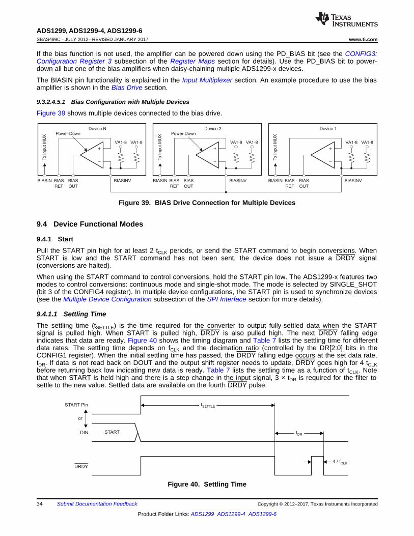
START
START Pin
DIN
4 / fCLK
DRDY
or
tDR
tSETTLE
BIASINVBIAS
OUT
BIAS
REF
BIASIN
VA1-8
Device 2
VA1-8
BIASINVBIAS
OUT
BIAS
REF
BIASIN
VA1-8
Device N
VA1-8
Power-Down Power-Down
BIASINVBIAS
OUT
BIAS
REF
BIASIN
VA1-8
Device 1
VA1-8
To Input M
UX
To Input M
UX
To Input M
UX
34
ADS1299, ADS1299-4, ADS1299-6SBAS499C –JULY 2012–REVISED JANUARY 2017 www.ti.com
Product Folder Links: ADS1299 ADS1299-4 ADS1299-6
Submit Documentation Feedback Copyright © 2012–2017, Texas Instruments Incorporated
If the bias function is not used, the amplifier can be powered down using the PD_BIAS bit (see the CONFIG3:Configuration Register 3 subsection of the Register Maps section for details). Use the PD_BIAS bit to power-down all but one of the bias amplifiers when daisy-chaining multiple ADS1299-x devices.
The BIASIN pin functionality is explained in the Input Multiplexer section. An example procedure to use the biasamplifier is shown in the Bias Drive section.
9.3.2.4.5.1 Bias Configuration with Multiple Devices
Figure 39 shows multiple devices connected to the bias drive.
Figure 39. BIAS Drive Connection for Multiple Devices
9.4 Device Functional Modes
9.4.1 StartPull the START pin high for at least 2 tCLK periods, or send the START command to begin conversions. WhenSTART is low and the START command has not been sent, the device does not issue a DRDY signal(conversions are halted).
When using the START command to control conversions, hold the START pin low. The ADS1299-x features twomodes to control conversions: continuous mode and single-shot mode. The mode is selected by SINGLE_SHOT(bit 3 of the CONFIG4 register). In multiple device configurations, the START pin is used to synchronize devices(see the Multiple Device Configuration subsection of the SPI Interface section for more details).
9.4.1.1 Settling TimeThe settling time (tSETTLE) is the time required for the converter to output fully-settled data when the STARTsignal is pulled high. When START is pulled high, DRDY is also pulled high. The next DRDY falling edgeindicates that data are ready. Figure 40 shows the timing diagram and Table 7 lists the settling time for differentdata rates. The settling time depends on fCLK and the decimation ratio (controlled by the DR[2:0] bits in theCONFIG1 register). When the initial settling time has passed, the DRDY falling edge occurs at the set data rate,tDR. If data is not read back on DOUT and the output shift register needs to update, DRDY goes high for 4 tCLKbefore returning back low indicating new data is ready. Table 7 lists the settling time as a function of tCLK. Notethat when START is held high and there is a step change in the input signal, 3 × tDR is required for the filter tosettle to the new value. Settled data are available on the fourth DRDY pulse.
Figure 40. Settling Time

DRDY
DOUT
SCLK
Bit 215 Bit 214 Bit 213X
35
ADS1299, ADS1299-4, ADS1299-6www.ti.com SBAS499C –JULY 2012–REVISED JANUARY 2017
Product Folder Links: ADS1299 ADS1299-4 ADS1299-6
Submit Documentation FeedbackCopyright © 2012–2017, Texas Instruments Incorporated
Device Functional Modes (continued)Table 7. Settling Time for Different Data Rates
DR[2:0] NORMAL MODE UNIT000 521 tCLK
001 1033 tCLK
010 2057 tCLK
011 4105 tCLK
100 8201 tCLK
101 16393 tCLK
110 32777 tCLK
9.4.2 Reset (RESET)There are two methods to reset the ADS1299-x: pull the RESET pin low, or send the RESET command. Whenusing the RESET pin, make sure to follow the minimum pulse duration timing specifications before taking the pinback high. The RESET command takes effect on the eighth SCLK falling edge of the command. After a reset, 18tCLK cycles are required to complete initialization of the configuration registers to default states and start theconversion cycle. Note that an internal reset is automatically issued to the digital filter whenever the CONFIG1register is set to a new value with a WREG command.
9.4.3 Power-Down (PWDN)When PWDN is pulled low, all on-chip circuitry is powered down. To exit power-down mode, take the PWDN pinhigh. Upon exiting from power-down mode, the internal oscillator and the reference require time to wake up.During power-down, the external clock is recommended to be shut down to save power.
9.4.4 Data Retrieval
9.4.4.1 Data Ready (DRDY)DRDY is an output signal which transitions from high to low indicating new conversion data are ready. The CSsignal has no effect on the data ready signal. DRDY behavior is determined by whether the device is in RDATACmode or the RDATA command is used to read data on demand. (See the RDATAC: Read Data Continuous andRDATA: Read Data subsections of the SPI Command Definitions section for further details).
When reading data with the RDATA command, the read operation can overlap the next DRDY occurrencewithout data corruption.
The START pin or the START command places the device either in normal data capture mode or pulse datacapture mode.
Figure 41 shows the relationship between DRDY, DOUT, and SCLK during data retrieval (in case of anADS1299). DOUT is latched out at the SCLK rising edge. DRDY is pulled high at the SCLK falling edge. Notethat DRDY goes high on the first SCLK falling edge, regardless of whether data are being retrieved from thedevice or a command is being sent through the DIN pin.
Figure 41. DRDY with Data Retrieval (CS = 0)
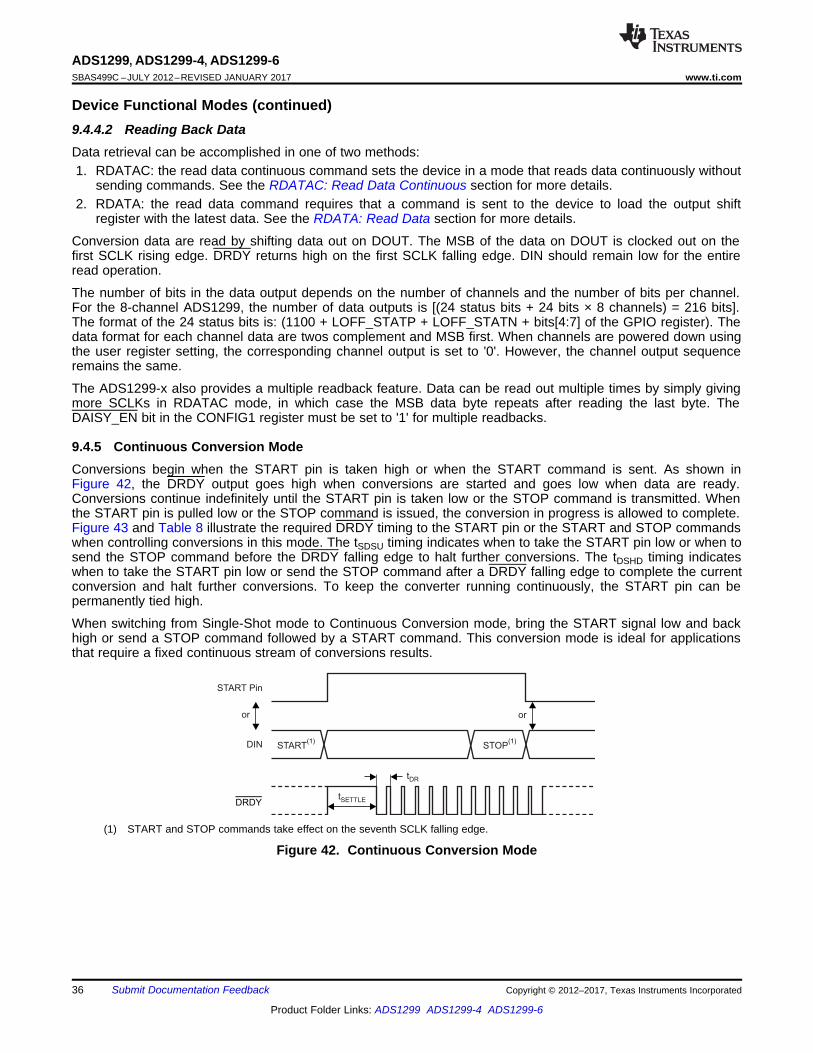
START(1)
START Pin
DIN
tDR
tSETTLEDRDY
STOP(1)
or or
36
ADS1299, ADS1299-4, ADS1299-6SBAS499C –JULY 2012–REVISED JANUARY 2017 www.ti.com
Product Folder Links: ADS1299 ADS1299-4 ADS1299-6
Submit Documentation Feedback Copyright © 2012–2017, Texas Instruments Incorporated
Device Functional Modes (continued)9.4.4.2 Reading Back DataData retrieval can be accomplished in one of two methods:1. RDATAC: the read data continuous command sets the device in a mode that reads data continuously without
sending commands. See the RDATAC: Read Data Continuous section for more details.2. RDATA: the read data command requires that a command is sent to the device to load the output shift
register with the latest data. See the RDATA: Read Data section for more details.
Conversion data are read by shifting data out on DOUT. The MSB of the data on DOUT is clocked out on thefirst SCLK rising edge. DRDY returns high on the first SCLK falling edge. DIN should remain low for the entireread operation.
The number of bits in the data output depends on the number of channels and the number of bits per channel.For the 8-channel ADS1299, the number of data outputs is [(24 status bits + 24 bits × 8 channels) = 216 bits].The format of the 24 status bits is: (1100 + LOFF_STATP + LOFF_STATN + bits[4:7] of the GPIO register). Thedata format for each channel data are twos complement and MSB first. When channels are powered down usingthe user register setting, the corresponding channel output is set to '0'. However, the channel output sequenceremains the same.
The ADS1299-x also provides a multiple readback feature. Data can be read out multiple times by simply givingmore SCLKs in RDATAC mode, in which case the MSB data byte repeats after reading the last byte. TheDAISY_EN bit in the CONFIG1 register must be set to '1' for multiple readbacks.
9.4.5 Continuous Conversion ModeConversions begin when the START pin is taken high or when the START command is sent. As shown inFigure 42, the DRDY output goes high when conversions are started and goes low when data are ready.Conversions continue indefinitely until the START pin is taken low or the STOP command is transmitted. Whenthe START pin is pulled low or the STOP command is issued, the conversion in progress is allowed to complete.Figure 43 and Table 8 illustrate the required DRDY timing to the START pin or the START and STOP commandswhen controlling conversions in this mode. The tSDSU timing indicates when to take the START pin low or when tosend the STOP command before the DRDY falling edge to halt further conversions. The tDSHD timing indicateswhen to take the START pin low or send the STOP command after a DRDY falling edge to complete the currentconversion and halt further conversions. To keep the converter running continuously, the START pin can bepermanently tied high.
When switching from Single-Shot mode to Continuous Conversion mode, bring the START signal low and backhigh or send a STOP command followed by a START command. This conversion mode is ideal for applicationsthat require a fixed continuous stream of conversions results.
(1) START and STOP commands take effect on the seventh SCLK falling edge.
Figure 42. Continuous Conversion Mode
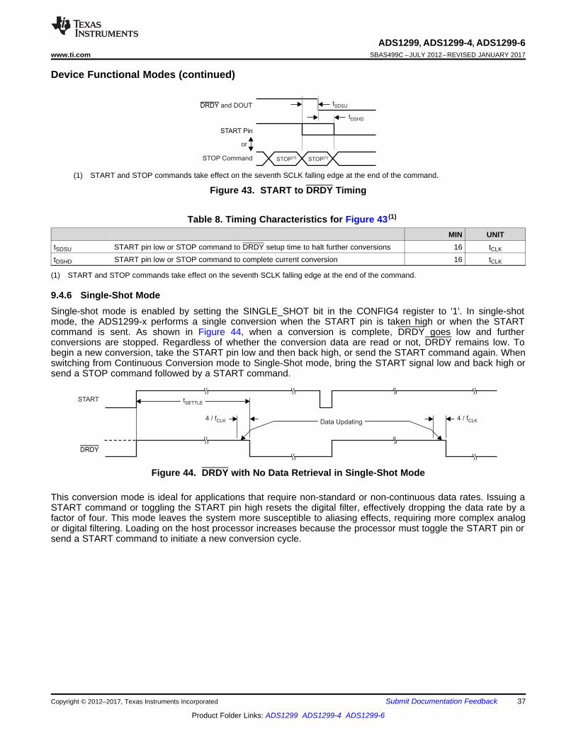
START
DRDY
4 / fCLK 4 / fCLKData Updating
tSETTLE
tSDSU
tDSHD
STOP Command
DRDY and DOUT
START Pin
or
STOP(1)STOP(1)
37
ADS1299, ADS1299-4, ADS1299-6www.ti.com SBAS499C –JULY 2012–REVISED JANUARY 2017
Product Folder Links: ADS1299 ADS1299-4 ADS1299-6
Submit Documentation FeedbackCopyright © 2012–2017, Texas Instruments Incorporated
Device Functional Modes (continued)
(1) START and STOP commands take effect on the seventh SCLK falling edge at the end of the command.
(1) START and STOP commands take effect on the seventh SCLK falling edge at the end of the command.
Figure 43. START to DRDY Timing
Table 8. Timing Characteristics for Figure 43 (1)
MIN UNITtSDSU START pin low or STOP command to DRDY setup time to halt further conversions 16 tCLK
tDSHD START pin low or STOP command to complete current conversion 16 tCLK
9.4.6 Single-Shot ModeSingle-shot mode is enabled by setting the SINGLE_SHOT bit in the CONFIG4 register to '1'. In single-shotmode, the ADS1299-x performs a single conversion when the START pin is taken high or when the STARTcommand is sent. As shown in Figure 44, when a conversion is complete, DRDY goes low and furtherconversions are stopped. Regardless of whether the conversion data are read or not, DRDY remains low. Tobegin a new conversion, take the START pin low and then back high, or send the START command again. Whenswitching from Continuous Conversion mode to Single-Shot mode, bring the START signal low and back high orsend a STOP command followed by a START command.
Figure 44. DRDY with No Data Retrieval in Single-Shot Mode
This conversion mode is ideal for applications that require non-standard or non-continuous data rates. Issuing aSTART command or toggling the START pin high resets the digital filter, effectively dropping the data rate by afactor of four. This mode leaves the system more susceptible to aliasing effects, requiring more complex analogor digital filtering. Loading on the host processor increases because the processor must toggle the START pin orsend a START command to initiate a new conversion cycle.

38
ADS1299, ADS1299-4, ADS1299-6SBAS499C –JULY 2012–REVISED JANUARY 2017 www.ti.com
Product Folder Links: ADS1299 ADS1299-4 ADS1299-6
Submit Documentation Feedback Copyright © 2012–2017, Texas Instruments Incorporated
9.5 Programming
9.5.1 Data FormatThe device provides 24 bits of data in binary twos complement format. The size of one code (LSB) is calculatedusing Equation 8.
1 LSB = (2 × VREF / Gain) / 224 = +FS / 223 (8)
A positive full-scale input produces an output code of 7FFFFFh and the negative full-scale input produces anoutput code of 800000h. The output clips at these codes for signals exceeding full-scale. Table 9 summarizes theideal output codes for different input signals. All 24 bits toggle when the analog input is at positive or negativefull-scale.
(1) Excludes effects of noise, linearity, offset, and gain error.
Table 9. Ideal Output Code versus Input SignalINPUT SIGNAL, VIN
(INxP - INxN) IDEAL OUTPUT CODE (1)
≥ FS 7FFFFFh+FS / (223 – 1) 000001h
0 000000h–FS / (223 – 1) FFFFFFh
≤ –FS (223 / 223 – 1) 800000h
9.5.2 SPI Interface
The SPI-compatible serial interface consists of four signals: CS, SCLK, DIN, and DOUT. The interface readsconversion data, reads and writes registers, and controls ADS1299-x operation. The data-ready output, DRDY(see the Data Ready (DRDY) section), is used as a status signal to indicate when data are ready. DRDY goeslow when new data are available.
9.5.2.1 Chip Select (CS)The CS pin activates SPI communication. CS must be low before data transactions and must stay low for theentire SPI communication period. When CS is high, the DOUT pin enters a high-impedance state. Therefore,reading and writing to the serial interface are ignored and the serial interface is reset. DRDY pin operation isindependent of CS. DRDY still indicates that a new conversion has completed and is forced high as a responseto SCLK, even if CS is high.
Taking CS high deactivates only the SPI communication with the device and the serial interface is reset. Dataconversion continues and the DRDY signal can be monitored to check if a new conversion result is ready. Amaster device monitoring the DRDY signal can select the appropriate slave device by pulling the CS pin low.After the serial communication is finished, always wait four or more tCLK cycles before taking CS high.
9.5.2.2 Serial Clock (SCLK)SCLK provides the clock for serial communication. SCLK is a Schmitt-trigger input, but TI recommends keepingSCLK as free from noise as possible to prevent glitches from inadvertently shifting the data. Data are shifted intoDIN on the falling edge of SCLK and shifted out of DOUT on the rising edge of SCLK.
The absolute maximum SCLK limit is specified in Figure 1. When shifting in commands with SCLK, make surethat the entire set of SCLKs is issued to the device. Failure to do so can result in the device serial interface beingplaced into an unknown state requiring CS to be taken high to recover.
For a single device, the minimum speed required for SCLK depends on the number of channels, number of bitsof resolution, and output data rate. (For multiple cascaded devices, see the Cascaded Mode subsection of theMultiple Device Configuration section.)
For example, if the ADS1299 is used in a 500-SPS mode (8 channels, 24-bit resolution), the minimum SCLKspeed is 110 kHz.

CS
SCLK
DRDY
DOUT STAT
24-Bit 24-Bit 24-Bit 24-Bit 24-Bit 24-Bit 24-Bit 24-Bit 24-Bit
CH1 CH2 CH3 CH4 CH5 CH6 CH7 CH8
216 SCLKs
DIN
t <SCLK
t 4 tDR CLK
-
N N + 24BITS CHANNELS
´
39
ADS1299, ADS1299-4, ADS1299-6www.ti.com SBAS499C –JULY 2012–REVISED JANUARY 2017
Product Folder Links: ADS1299 ADS1299-4 ADS1299-6
Submit Documentation FeedbackCopyright © 2012–2017, Texas Instruments Incorporated
Data retrieval can be accomplished either by placing the device in RDATAC mode or by issuing an RDATAcommand for data on demand. The SCLK rate limitation in Equation 9 applies to RDATAC. For the RDATAcommand, the limitation applies if data must be read in between two consecutive DRDY signals. Equation 9assumes that there are no other commands issued in between data captures.
(9)
9.5.2.3 Data Input (DIN)DIN is used along with SCLK to send data to the device. Data on DIN are shifted into the device on the fallingedge of SCLK.
The communication of this device is full-duplex in nature. The device monitors commands shifted in even whendata are being shifted out. Data that are present in the output shift register are shifted out when sending in acommand. Therefore, make sure that whatever is being sent on the DIN pin is valid when shifting out data. Whenno command is to be sent to the device when reading out data, send the NOP command on DIN. Make sure thatthe tSDECODE timing is met in the Sending Multi-Byte Commands section when sending multiple byte commandson DIN.
9.5.2.4 Data Output (DOUT)DOUT is used with SCLK to read conversion and register data from the device. Data are clocked out on therising edge of SCLK, MSB first. DOUT goes to a high-impedance state when CS is high. Figure 45 shows theADS1299 data output protocol.
Figure 45. SPI Bus Data Output

40
ADS1299, ADS1299-4, ADS1299-6SBAS499C –JULY 2012–REVISED JANUARY 2017 www.ti.com
Product Folder Links: ADS1299 ADS1299-4 ADS1299-6
Submit Documentation Feedback Copyright © 2012–2017, Texas Instruments Incorporated
(1) When in RDATAC mode, the RREG command is ignored.(2) n nnnn = number of registers to be read or written – 1. For example, to read or write three registers, set n nnnn = 0 (0010). r rrrr =
starting register address for read or write commands.
9.5.3 SPI Command DefinitionsThe ADS1299-x provides flexible configuration control. The commands, summarized in Table 10, control andconfigure device operation. The commands are stand-alone, except for the register read and write operationsthat require a second command byte plus data. CS can be taken high or held low between commands but muststay low for the entire command operation (especially for multi-byte commands). System commands and theRDATA command are decoded by the device on the seventh SCLK falling edge. The register read and writecommands are decoded on the eighth SCLK falling edge. Be sure to follow SPI timing requirements when pullingCS high after issuing a command.
Table 10. Command DefinitionsCOMMAND DESCRIPTION FIRST BYTE SECOND BYTESystem CommandsWAKEUP Wake-up from standby mode 0000 0010 (02h)STANDBY Enter standby mode 0000 0100 (04h)RESET Reset the device 0000 0110 (06h)START Start and restart (synchronize) conversions 0000 1000 (08h)STOP Stop conversion 0000 1010 (0Ah)Data Read Commands
RDATAC Enable Read Data Continuous mode.This mode is the default mode at power-up. (1) 0001 0000 (10h)
SDATAC Stop Read Data Continuously mode 0001 0001 (11h)RDATA Read data by command; supports multiple read back. 0001 0010 (12h)Register Read CommandsRREG Read n nnnn registers starting at address r rrrr 001r rrrr (2xh) (2) 000n nnnn (2)
WREG Write n nnnn registers starting at address r rrrr 010r rrrr (4xh) (2) 000n nnnn (2)
9.5.3.1 Sending Multi-Byte CommandsThe ADS1299-x serial interface decodes commands in bytes and requires 4 tCLK cycles to decode and execute.Therefore, when sending multi-byte commands (such as RREG or WREG), a 4 tCLK period must separate theend of one byte (or command) and the next.
Assuming CLK is 2.048 MHz, then tSDECODE (4 tCLK) is 1.96 µs. When SCLK is 16 MHz, one byte can betransferred in 500 ns. This byte transfer time does not meet the tSDECODE specification; therefore, a delay must beinserted so the end of the second byte arrives 1.46 µs later. If SCLK is 4 MHz, one byte is transferred in 2 µs.Because this transfer time exceeds the tSDECODE specification, the processor can send subsequent bytes withoutdelay. In this later scenario, the serial port can be programmed to move from single-byte transfers per cycle tomultiple bytes.
9.5.3.2 WAKEUP: Exit STANDBY ModeThe WAKEUP command exits low-power standby mode; see the STANDBY: Enter STANDBY Mode subsectionof the SPI Command Definitions section. Time is required when exiting standby mode (see the ElectricalCharacteristics for details). There are no SCLK rate restrictions for this command and can be issued at anytime. Any following commands must be sent after a delay of 4 tCLK cycles.
9.5.3.3 STANDBY: Enter STANDBY ModeThe STANDBY command enters low-power standby mode. All parts of the circuit are shut down except for thereference section. The standby mode power consumption is specified in the Electrical Characteristics. There areno SCLK rate restrictions for this command and can be issued at any time. Do not send any othercommands other than the wakeup command after the device enters standby mode.

START
DRDY
CS
SCLK
DIN
tUPDATE
DOUTHi-Z
RDATAC
Status Register + 8-Channel Data (216 Bits) Next Data
41
ADS1299, ADS1299-4, ADS1299-6www.ti.com SBAS499C –JULY 2012–REVISED JANUARY 2017
Product Folder Links: ADS1299 ADS1299-4 ADS1299-6
Submit Documentation FeedbackCopyright © 2012–2017, Texas Instruments Incorporated
9.5.3.4 RESET: Reset Registers to Default ValuesThe RESET command resets the digital filter cycle and returns all register settings to default values. See theReset (RESET) subsection of the SPI Interface section for more details. There are no SCLK rate restrictionsfor this command and can be issued at any time. 18 tCLK cycles are required to execute the RESETcommand. Avoid sending any commands during this time.
9.5.3.5 START: Start ConversionsThe START command starts data conversions. Tie the START pin low to control conversions by command. Ifconversions are in progress, this command has no effect. The STOP command stops conversions. If the STARTcommand is immediately followed by a STOP command, then there must be a 4-tCLK cycle delay between them.When the START command is sent to the device, keep the START pin low until the STOP command is issued.(See the Start subsection of the SPI Interface section for more details.) There are no SCLK rate restrictionsfor this command and can be issued at any time.
9.5.3.6 STOP: Stop ConversionsThe STOP command stops conversions. Tie the START pin low to control conversions by command. When theSTOP command is sent, the conversion in progress completes and further conversions are stopped. Ifconversions are already stopped, this command has no effect. There are no SCLK rate restrictions for thiscommand and can be issued at any time.
9.5.3.7 RDATAC: Read Data Continuous
The RDATAC command enables conversion data output on each DRDY without the need to issue subsequentread data commands. This mode places the conversion data in the output register and may be shifted outdirectly. The read data continuous mode is the device default mode; the device defaults to this mode on power-up.
RDATAC mode is cancelled by the Stop Read Data Continuous command. If the device is in RDATAC mode, aSDATAC command must be issued before any other commands can be sent to the device. There are no SCLKrate restrictions for this command. However, subsequent data retrieval SCLKs or the SDATAC commandshould wait at least 4 tCLK cycles before completion (see the Sending Multi-Byte Commands section). RDATACtiming is illustrated in Figure 46. As depicted in Figure 46, there is a keep out zone of 4 tCLK cycles around theDRDY pulse where this command cannot be issued in. If no data are retrieved from the device, DOUT andDRDY behave similarly in this mode. To retrieve data from the device after the RDATAC command is issued,make sure either the START pin is high or the START command is issued. Figure 46 shows the recommendedway to use the RDATAC command. RDATAC is ideally-suited for applications such as data loggers or recorders,where registers are set one time and do not need to be reconfigured.
(1) tUPDATE = 4 / fCLK. Do not read data during this time.
Figure 46. RDATAC Usage

Hi-Z
START
DRDY
CS
SCLK
DIN
DOUT
RDATA
Status Register+ 8-Channel Data (216 Bits)
RDATA
42
ADS1299, ADS1299-4, ADS1299-6SBAS499C –JULY 2012–REVISED JANUARY 2017 www.ti.com
Product Folder Links: ADS1299 ADS1299-4 ADS1299-6
Submit Documentation Feedback Copyright © 2012–2017, Texas Instruments Incorporated
9.5.3.8 SDATAC: Stop Read Data ContinuousThe SDATAC command cancels the Read Data Continuous mode. There are no SCLK rate restrictions forthis command, but the next command must wait for 4 tCLK cycles before completion.
9.5.3.9 RDATA: Read DataThe RDATA command loads the output shift register with the latest data when not in Read Data Continuousmode. Issue this command after DRDY goes low to read the conversion result. There are no SCLK raterestrictions for this command, and there is no wait time needed for the subsequent commands or data retrievalSCLKs. To retrieve data from the device after the RDATA command is issued, make sure either the START pinis high or the START command is issued. When reading data with the RDATA command, the read operation canoverlap the next DRDY occurrence without data corruption. Figure 47 shows the recommended way to use theRDATA command. RDATA is best suited for ECG- and EEG-type systems, where register settings must be reador changed often between conversion cycles.
Figure 47. RDATA Usage

1 9 17 25
CS
SCLK
DIN BYTE 1 BYTE 2 REG DATA 1 REG DATA 2
DOUT
1 9 17 25
CS
SCLK
DIN BYTE 1 BYTE 2
DOUT REG DATA REG DATA + 1
43
ADS1299, ADS1299-4, ADS1299-6www.ti.com SBAS499C –JULY 2012–REVISED JANUARY 2017
Product Folder Links: ADS1299 ADS1299-4 ADS1299-6
Submit Documentation FeedbackCopyright © 2012–2017, Texas Instruments Incorporated
9.5.3.10 RREG: Read From RegisterThis command reads register data. The Register Read command is a two-byte command followed by the registerdata output. The first byte contains the command and register address. The second command byte specifies thenumber of registers to read – 1.
First command byte: 001r rrrr, where r rrrr is the starting register address.
Second command byte: 000n nnnn, where n nnnn is the number of registers to read – 1.
The 17th SCLK rising edge of the operation clocks out the MSB of the first register, as shown in Figure 48. Whenthe device is in read data continuous mode, an SDATAC command must be issued before the RREG commandcan be issued. The RREG command can be issued any time. However, because this command is a multi-bytecommand, there are SCLK rate restrictions depending on how the SCLKs are issued to meet the tSDECODE timing.See the Serial Clock (SCLK) subsection of the SPI Interface section for more details. Note that CS must be lowfor the entire command.
Figure 48. RREG Command Example: Read Two Registers Starting from Register 00h (ID Register)(BYTE 1 = 0010 0000, BYTE 2 = 0000 0001)
9.5.3.11 WREG: Write to RegisterThis command writes register data. The Register Write command is a two-byte command followed by the registerdata input. The first byte contains the command and register address. The second command byte specifies thenumber of registers to write – 1.
First command byte: 010r rrrr, where r rrrr is the starting register address.
Second command byte: 000n nnnn, where n nnnn is the number of registers to write – 1.
After the command bytes, the register data follows (in MSB-first format), as shown in Figure 49. The WREGcommand can be issued any time. However, because this command is a multi-byte command, there are SCLKrate restrictions depending on how the SCLKs are issued to meet the tSDECODE timing. See the Serial Clock(SCLK) subsection of the SPI Interface section for more details. Note that CS must be low for the entirecommand.
Figure 49. WREG Command Example: Write Two Registers Starting from 00h (ID Register)(BYTE 1 = 0100 0000, BYTE 2 = 0000 0001)

44
ADS1299, ADS1299-4, ADS1299-6SBAS499C –JULY 2012–REVISED JANUARY 2017 www.ti.com
Product Folder Links: ADS1299 ADS1299-4 ADS1299-6
Submit Documentation Feedback Copyright © 2012–2017, Texas Instruments Incorporated
(1) Register or bit only available in the ADS1299-6 and ADS1299. Register bits set to 0h or 00h in the ADS1299-4.(2) Register or bit only available in the ADS1299. Register bits set to 0h or 00h in the ADS1299-4 and ADS1299-6.
9.6 Register MapsTable 11 describes the various ADS1299-x registers.
Table 11. Register Assignments
ADDRESS REGISTERDEFAULTSETTING
REGISTER BITS
7 6 5 4 3 2 1 0
Read Only ID Registers
00h ID xxh REV_ID[2:0] 1 DEV_ID[1:0] NU_CH[1:0]
Global Settings Across Channels
01h CONFIG1 96h 1 DAISY_EN CLK_EN 1 0 DR[2:0]
02h CONFIG2 C0h 1 1 0 INT_CAL 0 CAL_AMP0 CAL_FREQ[1:0]
03h CONFIG3 60h PD_REFBUF 1 1 BIAS_MEAS BIASREF_INT PD_BIAS BIAS_LOFF_SENS BIAS_STAT
04h LOFF 00h COMP_TH[2:0] 0 ILEAD_OFF[1:0] FLEAD_OFF[1:0]
Channel-Specific Settings
05h CH1SET 61h PD1 GAIN1[2:0] SRB2 MUX1[2:0]
06h CH2SET 61h PD2 GAIN2[2:0] SRB2 MUX2[2:0]
07h CH3SET 61h PD3 GAIN3[2:0] SRB2 MUX3[2:0]
08h CH4SET 61h PD4 GAIN4[2:0] SRB2 MUX4[2:0]
09h CH5SET (1) 61h PD5 GAIN5[2:0] SRB2 MUX5[2:0]
0Ah CH6SET (1) 61h PD6 GAIN6[2:0] SRB2 MUX6[2:0]
0Bh CH7SET (2) 61h PD7 GAIN7[2:0] SRB2 MUX7[2:0]
0Ch CH8SET (2) 61h PD8 GAIN8[2:0] SRB2 MUX8[2:0]
0Dh BIAS_SENSP 00h BIASP8 (2) BIASP7 (2) BIASP6 (1) BIASP5 (1) BIASP4 BIASP3 BIASP2 BIASP1
0Eh BIAS_SENSN 00h BIASN8(2) BIASN7(2) BIASN6(1) BIASN5(1) BIASN4 BIASN3 BIASN2 BIASN1
0Fh LOFF_SENSP 00h LOFFP8(2) LOFFP7(2) LOFFP6(1) LOFFP5(1) LOFFP4 LOFFP3 LOFFP2 LOFFP1
10h LOFF_SENSN 00h LOFFM8(2) LOFFM7(2) LOFFM6(1) LOFFM5(1) LOFFM4 LOFFM3 LOFFM2 LOFFM1
11h LOFF_FLIP 00h LOFF_FLIP8(2) LOFF_FLIP7(2) LOFF_FLIP6(1) LOFF_FLIP5(1) LOFF_FLIP4 LOFF_FLIP3 LOFF_FLIP2 LOFF_FLIP1
Lead-Off Status Registers (Read-Only Registers)
12h LOFF_STATP 00h IN8P_OFF IN7P_OFF IN6P_OFF IN5P_OFF IN4P_OFF IN3P_OFF IN2P_OFF IN1P_OFF
13h LOFF_STATN 00h IN8M_OFF IN7M_OFF IN6M_OFF IN5M_OFF IN4M_OFF IN3M_OFF IN2M_OFF IN1M_OFF
GPIO and OTHER Registers
14h GPIO 0Fh GPIOD[4:1] GPIOC[4:1]
15h MISC1 00h 0 0 SRB1 0 0 0 0 0
16h MISC2 00h 0 0 0 0 0 0 0 0
17h CONFIG4 00h 0 0 0 0 SINGLE_SHOT 0 PD_LOFF_
COMP 0

45
ADS1299, ADS1299-4, ADS1299-6www.ti.com SBAS499C –JULY 2012–REVISED JANUARY 2017
Product Folder Links: ADS1299 ADS1299-4 ADS1299-6
Submit Documentation FeedbackCopyright © 2012–2017, Texas Instruments Incorporated
9.6.1 User Register DescriptionThe read-only ID control register is programmed during device manufacture to indicate device characteristics.
9.6.1.1 ID: ID Control Register (address = 00h) (reset = xxh)
Figure 50. ID Control Register
7 6 5 4 3 2 1 0REV_ID[2:0] 1 DEV_ID[1:0] NU_CH[1:0]
R-xh R-1h R-3h R-xhLEGEND: R/W = Read/Write; R = Read only; -n = value after reset
Table 12. ID Control Register Field DescriptionsBit Field Type Reset Description7:5 REV_ID[2:0] R xh Reserved.
These bits indicate the revision of the device and are subject tochange without notice.
4 Reserved R 1h Reserved.Always read 1.
3:2 DEV_ID[1:0] R 3h Device Identification.These bits indicates the device.11 : ADS1299-x
1:0 NU_CH[1:0] R xh Number of Channels.These bits indicates number of channels.00 : 4-channel ADS1299-401 : 6-channel ADS1299-610 : 8-channel ADS1299

46
ADS1299, ADS1299-4, ADS1299-6SBAS499C –JULY 2012–REVISED JANUARY 2017 www.ti.com
Product Folder Links: ADS1299 ADS1299-4 ADS1299-6
Submit Documentation Feedback Copyright © 2012–2017, Texas Instruments Incorporated
9.6.1.2 CONFIG1: Configuration Register 1 (address = 01h) (reset = 96h)This register configures the DAISY_EN bit, clock, and data rate.
Figure 51. CONFIG1: Configuration Register 1
7 6 5 4 3 2 1 01 DAISY_EN CLK_EN 1 0 DR[2:0]
R/W-1h R/W-0h R/W-0h R/W-1h R/W-0h R/W-6hLEGEND: R/W = Read/Write; R = Read only; -n = value after reset
(1) Additional power is consumed when driving external devices.
Table 13. Configuration Register 1 Field DescriptionsBit Field Type Reset Description7 Reserved R/W 1h Reserved
Always write 1h6 DAISY_EN R/W 0h Daisy-chain or multiple readback mode
This bit determines which mode is enabled.0 : Daisy-chain mode1 : Multiple readback mode
5 CLK_EN R/W 0h CLK connection (1)
This bit determines if the internal oscillator signal is connected tothe CLK pin when the CLKSEL pin = 1.0 : Oscillator clock output disabled1 : Oscillator clock output enabled
4:3 Reserved R/W 2h ReservedAlways write 2h
2:0 DR[2:0] R/W 6h Output data rateThese bits determine the output data rate of the device. fMOD =fCLK / 2.000 : fMOD / 64 (16 kSPS)001 : fMOD / 128 (8 kSPS)010 : fMOD / 256 (4 kSPS)011 : fMOD / 512 (2 kSPS)100 : fMOD / 1024 (1 kSPS)101 : fMOD / 2048 (500 SPS)110 : fMOD / 4096 (250 SPS)111 : Reserved (do not use)

47
ADS1299, ADS1299-4, ADS1299-6www.ti.com SBAS499C –JULY 2012–REVISED JANUARY 2017
Product Folder Links: ADS1299 ADS1299-4 ADS1299-6
Submit Documentation FeedbackCopyright © 2012–2017, Texas Instruments Incorporated
9.6.1.3 CONFIG2: Configuration Register 2 (address = 02h) (reset = C0h)This register configures the test signal generation. See the Input Multiplexer section for more details.
Figure 52. CONFIG2: Configuration Register 2
7 6 5 4 3 2 1 01 1 0 INT_CAL 0 CAL_AMP CAL_FREQ[1:0]
R/W-1h R/W-1h R/W-0h R/W-0h R/W-0h R/W-0h R/W-0hLEGEND: R/W = Read/Write; R = Read only; -n = value after reset
Table 14. Configuration Register 2 Field DescriptionsBit Field Type Reset Description7:5 Reserved R/W 6h Reserved
Always write 6h4 INT_CAL R/W 0h TEST source
This bit determines the source for the test signal.0 : Test signals are driven externally1 : Test signals are generated internally
3 Reserved R/W 0h ReservedAlways write 0h
2 CAL_AMP R/W 0h Test signal amplitudeThese bits determine the calibration signal amplitude.0 : 1 × –(VREFP – VREFN) / 24001 : 2 × –(VREFP – VREFN) / 2400
1:0 CAL_FREQ[1:0] R/W 0h Test signal frequencyThese bits determine the calibration signal frequency.00 : Pulsed at fCLK / 221
01 : Pulsed at fCLK / 220
10 : Do not use11 : At dc

48
ADS1299, ADS1299-4, ADS1299-6SBAS499C –JULY 2012–REVISED JANUARY 2017 www.ti.com
Product Folder Links: ADS1299 ADS1299-4 ADS1299-6
Submit Documentation Feedback Copyright © 2012–2017, Texas Instruments Incorporated
9.6.1.4 CONFIG3: Configuration Register 3 (address = 03h) (reset = 60h)Configuration register 3 configures either an internal or exteral reference and BIAS operation.
Figure 53. CONFIG3: Configuration Register 3
7 6 5 4 3 2 1 0
PD_REFBUF 1 1 BIAS_MEAS BIASREF_INT PD_BIAS BIAS_LOFF_SENS BIAS_STAT
R/W-0h R/W-1h R/W-1h R/W-0h R/W-0h R/W-0h R/W-0h R-0hLEGEND: R/W = Read/Write; R = Read only; -n = value after reset
Table 15. Configuration Register 3 Field DescriptionsBit Field Type Reset Description7 PD_REFBUF R/W 0h Power-down reference buffer
This bit determines the power-down reference buffer state.0 : Power-down internal reference buffer1 : Enable internal reference buffer
6:5 Reserved R/W 3h ReservedAlways write 3h.
4 BIAS_MEAS R/W 0h BIAS measurementThis bit enables BIAS measurement. The BIAS signal may bemeasured with any channel.0 : Open1 : BIAS_IN signal is routed to the channel that has theMUX_Setting 010 (VREF)
3 BIASREF_INT R/W 0h BIASREF signalThis bit determines the BIASREF signal source.0 : BIASREF signal fed externally1 : BIASREF signal (AVDD + AVSS) / 2 generated internally
2 PD_BIAS R/W 0h BIAS buffer powerThis bit determines the BIAS buffer power state.0 : BIAS buffer is powered down1 : BIAS buffer is enabled
1 BIAS_LOFF_SENS R/W 0h BIAS sense functionThis bit enables the BIAS sense function.0 : BIAS sense is disabled1 : BIAS sense is enabled
0 BIAS_STAT R 0h BIAS lead-off statusThis bit determines the BIAS status.0 : BIAS is connected1 : BIAS is not connected

49
ADS1299, ADS1299-4, ADS1299-6www.ti.com SBAS499C –JULY 2012–REVISED JANUARY 2017
Product Folder Links: ADS1299 ADS1299-4 ADS1299-6
Submit Documentation FeedbackCopyright © 2012–2017, Texas Instruments Incorporated
9.6.1.5 LOFF: Lead-Off Control Register (address = 04h) (reset = 00h)The lead-off control register configures the lead-off detection operation.
Figure 54. LOFF: Lead-Off Control Register
7 6 5 4 3 2 1 0COMP_TH2[2:0] 0 ILEAD_OFF[1:0] FLEAD_OFF[1:0]
R/W-0h R/W-0h R/W-0h R/W-0hLEGEND: R/W = Read/Write; R = Read only; -n = value after reset
Table 16. Lead-Off Control Register Field DescriptionsBit Field Type Reset Description7:5 COMP_TH[2:0] R/W 0h Lead-off comparator threshold
Comparator positive side000 : 95%001 : 92.5%010 : 90%011 : 87.5%100 : 85%101 : 80%110 : 75%111 : 70%Comparator negative side000 : 5%001 : 7.5%010 : 10%011 : 12.5%100 : 15%101 : 20%110 : 25%111 : 30%
4 Reserved R/W 0h ReservedAlways write 0h.
3:2 ILEAD_OFF[1:0] R/W 0h Lead-off current magnitudeThese bits determine the magnitude of current for the currentlead-off mode.00 : 6 nA01 : 24 nA10 : 6 µA11 : 24 µA
1:0 FLEAD_OFF[1:0] R/W 0h Lead-off frequencyThese bits determine the frequency of lead-off detect for eachchannel.00 : DC lead-off detection01 : AC lead-off detection at 7.8 Hz (fCLK / 218)10 : AC lead-off detection at 31.2 Hz (fCLK / 216)11 : AC lead-off detection at fDR / 4

50
ADS1299, ADS1299-4, ADS1299-6SBAS499C –JULY 2012–REVISED JANUARY 2017 www.ti.com
Product Folder Links: ADS1299 ADS1299-4 ADS1299-6
Submit Documentation Feedback Copyright © 2012–2017, Texas Instruments Incorporated
9.6.1.6 CHnSET: Individual Channel Settings (n = 1 to 8) (address = 05h to 0Ch) (reset = 61h)The CH[1:8]SET control register configures the power mode, PGA gain, and multiplexer settings channels. Seethe Input Multiplexer section for details. CH[2:8]SET are similar to CH1SET, corresponding to the respectivechannels.
Figure 55. CHnSET: Individual Channel Settings Register
7 6 5 4 3 2 1 0PDn GAINn[2:0] SRB2 MUXn[2:0]
R/W-0h R/W-6h R/W-0h R/W-0hLEGEND: R/W = Read/Write; R = Read only; -n = value after reset
Table 17. Individual Channel Settings (n = 1 to 8) Field DescriptionsBit Field Type Reset Description7 PDn R/W 0h Power-down
This bit determines the channel power mode for thecorresponding channel.0 : Normal operation1 : Channel power-down.When powering down a channel, TI recommends that thechannel be set to input short by setting the appropriateMUXn[2:0] = 001 of the CHnSET register.
6:4 GAINn[2:0] R/W 6h PGA gainThese bits determine the PGA gain setting.000 : 1001 : 2010 : 4011 : 6100 : 8101 : 12110 : 24111 : Do not use
3 SRB2 R/W 0h SRB2 connectionThis bit determines the SRB2 connection for the correspondingchannel.0 : Open1 : Closed
2:0 MUXn[2:0] R/W 1h Channel inputThese bits determine the channel input selection.000 : Normal electrode input001 : Input shorted (for offset or noise measurements)010 : Used in conjunction with BIAS_MEAS bit for BIASmeasurements.011 : MVDD for supply measurement100 : Temperature sensor101 : Test signal110 : BIAS_DRP (positive electrode is the driver)111 : BIAS_DRN (negative electrode is the driver)

51
ADS1299, ADS1299-4, ADS1299-6www.ti.com SBAS499C –JULY 2012–REVISED JANUARY 2017
Product Folder Links: ADS1299 ADS1299-4 ADS1299-6
Submit Documentation FeedbackCopyright © 2012–2017, Texas Instruments Incorporated
9.6.1.7 BIAS_SENSP: Bias Drive Positive Derivation Register (address = 0Dh) (reset = 00h)This register controls the selection of the positive signals from each channel for bias voltage (BIAS) derivation.See the Bias Drive (DC Bias Circuit) section for details.
Registers bits[5:4] are not available for the ADS1299-4. Register bits[7:6] are not available for the ADS1299-4, orADS1299-6. Set unavailable bits for the associated device to 0 when writing to the register.
Figure 56. BIAS_SENSP: BIAS Positive Signal Derivation Register
7 6 5 4 3 2 1 0BIASP8 BIASP7 BIASP6 BIASP5 BIASP4 BIASP3 BIASP2 BIASP1R/W-0h R/W-0h R/W-0h R/W-0h R/W-0h R/W-0h R/W-0h R/W-0h
LEGEND: R/W = Read/Write; R = Read only; -n = value after reset
Table 18. BIAS Positive Signal Derivation Field DescriptionsBit Field Type Reset Description7 BIASP8 R/W 0h IN8P to BIAS
Route channel 8 positive signal into BIAS derivation0 : Disabled1 : Enabled
6 BIASP7 R/W 0h IN7P to BIASRoute channel 7 positive signal into BIAS derivation0 : Disabled1 : Enabled
5 BIASP6 R/W 0h IN6P to BIASRoute channel 6 positive signal into BIAS derivation0 : Disabled1 : Enabled
4 BIASP5 R/W 0h IN5P to BIASRoute channel 5 positive signal into BIAS derivation0 : Disabled1 : Enabled
3 BIASP4 R/W 0h IN4P to BIASRoute channel 4 positive signal into BIAS derivation0 : Disabled1 : Enabled
2 BIASP3 R/W 0h IN3P to BIASRoute channel 3 positive signal into BIAS derivation0 : Disabled1 : Enabled
1 BIASP2 R/W 0h IN2P to BIASRoute channel 2 positive signal into BIAS channel0 : Disabled1 : Enabled
0 BIASP1 R/W 0h IN1P to BIASRoute channel 1 positive signal into BIAS channel0 : Disabled1 : Enabled
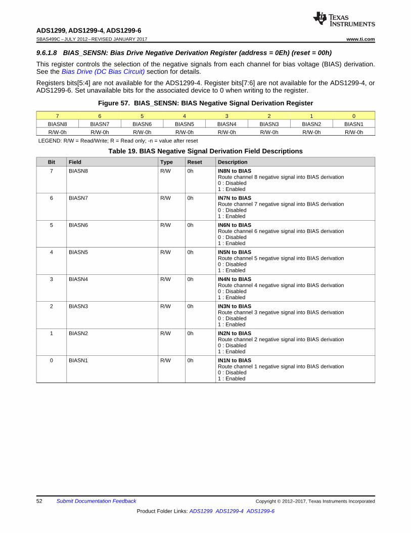
52
ADS1299, ADS1299-4, ADS1299-6SBAS499C –JULY 2012–REVISED JANUARY 2017 www.ti.com
Product Folder Links: ADS1299 ADS1299-4 ADS1299-6
Submit Documentation Feedback Copyright © 2012–2017, Texas Instruments Incorporated
9.6.1.8 BIAS_SENSN: Bias Drive Negative Derivation Register (address = 0Eh) (reset = 00h)This register controls the selection of the negative signals from each channel for bias voltage (BIAS) derivation.See the Bias Drive (DC Bias Circuit) section for details.
Registers bits[5:4] are not available for the ADS1299-4. Register bits[7:6] are not available for the ADS1299-4, orADS1299-6. Set unavailable bits for the associated device to 0 when writing to the register.
Figure 57. BIAS_SENSN: BIAS Negative Signal Derivation Register
7 6 5 4 3 2 1 0BIASN8 BIASN7 BIASN6 BIASN5 BIASN4 BIASN3 BIASN2 BIASN1R/W-0h R/W-0h R/W-0h R/W-0h R/W-0h R/W-0h R/W-0h R/W-0h
LEGEND: R/W = Read/Write; R = Read only; -n = value after reset
Table 19. BIAS Negative Signal Derivation Field DescriptionsBit Field Type Reset Description7 BIASN8 R/W 0h IN8N to BIAS
Route channel 8 negative signal into BIAS derivation0 : Disabled1 : Enabled
6 BIASN7 R/W 0h IN7N to BIASRoute channel 7 negative signal into BIAS derivation0 : Disabled1 : Enabled
5 BIASN6 R/W 0h IN6N to BIASRoute channel 6 negative signal into BIAS derivation0 : Disabled1 : Enabled
4 BIASN5 R/W 0h IN5N to BIASRoute channel 5 negative signal into BIAS derivation0 : Disabled1 : Enabled
3 BIASN4 R/W 0h IN4N to BIASRoute channel 4 negative signal into BIAS derivation0 : Disabled1 : Enabled
2 BIASN3 R/W 0h IN3N to BIASRoute channel 3 negative signal into BIAS derivation0 : Disabled1 : Enabled
1 BIASN2 R/W 0h IN2N to BIASRoute channel 2 negative signal into BIAS derivation0 : Disabled1 : Enabled
0 BIASN1 R/W 0h IN1N to BIASRoute channel 1 negative signal into BIAS derivation0 : Disabled1 : Enabled

53
ADS1299, ADS1299-4, ADS1299-6www.ti.com SBAS499C –JULY 2012–REVISED JANUARY 2017
Product Folder Links: ADS1299 ADS1299-4 ADS1299-6
Submit Documentation FeedbackCopyright © 2012–2017, Texas Instruments Incorporated
9.6.1.9 LOFF_SENSP: Positive Signal Lead-Off Detection Register (address = 0Fh) (reset = 00h)This register selects the positive side from each channel for lead-off detection. See the Lead-Off Detectionsection for details. The LOFF_STATP register bits are only valid if the corresponding LOFF_SENSP bits are setto 1.
Registers bits[5:4] are not available for the ADS1299-4. Register bits[7:6] are not available for the ADS1299-4, orADS1299-6. Set unavailable bits for the associated device to 0 when writing to the register.
Figure 58. LOFF_SENSP: Positive Signal Lead-Off Detection Register
7 6 5 4 3 2 1 0LOFFP8 LOFFP7 LOFFP6 LOFFP5 LOFFP4 LOFFP3 LOFFP2 LOFFP1R/W-0h R/W-0h R/W-0h R/W-0h R/W-0h R/W-0h R/W-0h R/W-0h
LEGEND: R/W = Read/Write; R = Read only; -n = value after reset
Table 20. Positive Signal Lead-Off Detection Field DescriptionsBit Field Type Reset Description7 LOFFP8 R/W 0h IN8P lead off
Enable lead-off detection on IN8P0 : Disabled1 : Enabled
6 LOFFP7 R/W 0h IN7P lead offEnable lead-off detection on IN7P0 : Disabled1 : Enabled
5 LOFFP6 R/W 0h IN6P lead offEnable lead-off detection on IN6P0 : Disabled1 : Enabled
4 LOFFP5 R/W 0h IN5P lead offEnable lead-off detection on IN5P0 : Disabled1 : Enabled
3 LOFFP4 R/W 0h IN4P lead offEnable lead-off detection on IN4P0 : Disabled1 : Enabled
2 LOFFP3 R/W 0h IN3P lead offEnable lead-off detection on IN3P0 : Disabled1 : Enabled
1 LOFFP2 R/W 0h IN2P lead offEnable lead-off detection on IN2P0 : Disabled1 : Enabled
0 LOFFP1 R/W 0h IN1P lead offEnable lead-off detection on IN1P0 : Disabled1 : Enabled

54
ADS1299, ADS1299-4, ADS1299-6SBAS499C –JULY 2012–REVISED JANUARY 2017 www.ti.com
Product Folder Links: ADS1299 ADS1299-4 ADS1299-6
Submit Documentation Feedback Copyright © 2012–2017, Texas Instruments Incorporated
9.6.1.10 LOFF_SENSN: Negative Signal Lead-Off Detection Register (address = 10h) (reset = 00h)This register selects the negative side from each channel for lead-off detection. See the Lead-Off Detectionsection for details. The LOFF_STATN register bits are only valid if the corresponding LOFF_SENSN bits are setto 1.
Registers bits[5:4] are not available for the ADS1299-4. Register bits[7:6] are not available for the ADS1299-4, orADS1299-6. Set unavailable bits for the associated device to 0 when writing to the register.
Figure 59. LOFF_SENSN: Negative Signal Lead-Off Detection Register
7 6 5 4 3 2 1 0LOFFM8 LOFFM7 LOFFM6 LOFFM5 LOFFM4 LOFFM3 LOFFM2 LOFFM1R/W-0h R/W-0h R/W-0h R/W-0h R/W-0h R/W-0h R/W-0h R/W-0h
LEGEND: R/W = Read/Write; R = Read only; -n = value after reset
Table 21. Negative Signal Lead-Off Detection Field DescriptionsBit Field Type Reset Description7 LOFFM8 R/W 0h IN8N lead off
Enable lead-off detection on IN8N0 : Disabled1 : Enabled
6 LOFFM7 R/W 0h IN7N lead offEnable lead-off detection on IN7N0 : Disabled1 : Enabled
5 LOFFM6 R/W 0h IN6N lead offEnable lead-off detection on IN6N0 : Disabled1 : Enabled
4 LOFFM5 R/W 0h IN5N lead offEnable lead-off detection on IN5N0 : Disabled1 : Enabled
3 LOFFM4 R/W 0h IN4N lead offEnable lead-off detectionn on IN4N0 : Disabled1 : Enabled
2 LOFFM3 R/W 0h IN3N lead offEnable lead-off detectionion on IN3N0 : Disabled1 : Enabled
1 LOFFM2 R/W 0h IN2N lead offEnable lead-off detectionction on IN2N0 : Disabled1 : Enabled
0 LOFFM1 R/W 0h IN1N lead offEnable lead-off detectionction on IN1N0 : Disabled1 : Enabled

55
ADS1299, ADS1299-4, ADS1299-6www.ti.com SBAS499C –JULY 2012–REVISED JANUARY 2017
Product Folder Links: ADS1299 ADS1299-4 ADS1299-6
Submit Documentation FeedbackCopyright © 2012–2017, Texas Instruments Incorporated
9.6.1.11 LOFF_FLIP: Lead-Off Flip Register (address = 11h) (reset = 00h)This register controls the direction of the current used for lead-off derivation. See the Lead-Off Detection sectionfor details.
Figure 60. LOFF_FLIP: Lead-Off Flip Register
7 6 5 4 3 2 1 0LOFF_FLIP8 LOFF_FLIP7 LOFF_FLIP6 LOFF_FLIP5 LOFF_FLIP4 LOFF_FLIP3 LOFF_FLIP2 LOFF_FLIP1
R/W-0h R/W-0h R/W-0h R/W-0h R/W-0h R/W-0h R/W-0h R/W-0hLEGEND: R/W = Read/Write; R = Read only; -n = value after reset
Table 22. Lead-Off Flip Register Field DescriptionsBit Field Type Reset Description7 LOFF_FLIP8 R/W 0h Channel 8 LOFF polarity flip
Flip the pull-up or pull-down polarity of the current source onchannel 8 for lead-off detection.0 : No flip = IN8P is pulled to AVDD and IN8N pulled to AVSS1 : Flipped = IN8P is pulled to AVSS and IN8N pulled to AVDD
6 LOFF_FLIP7 R/W 0h Channel 7 LOFF polarity flipFlip the pull-up or pull-down polarity of the current source onchannel 7 for lead-off detection.0 : No flip = IN7P is pulled to AVDD and IN7N pulled to AVSS1 : Flipped = IN7P is pulled to AVSS and IN7N pulled to AVDD
5 LOFF_FLIP6 R/W 0h Channel 6 LOFF polarity flipFlip the pull-up or pull-down polarity of the current source onchannel 6 for lead-off detection.0 : No flip = IN6P is pulled to AVDD and IN6N pulled to AVSS1 : Flipped = IN6P is pulled to AVSS and IN6N pulled to AVDD
4 LOFF_FLIP5 R/W 0h Channel 5 LOFF polarity flipFlip the pull-up or pull-down polarity of the current source onchannel 5 for lead-off detection.0 : No flip = IN5P is pulled to AVDD and IN5N pulled to AVSS1 : Flipped = IN5P is pulled to AVSS and IN5N pulled to AVDD
3 LOFF_FLIP4 R/W 0h Channel 4 LOFF polarity flipFlip the pull-up or pull-down polarity of the current source onchannel 4 for lead-off detection.0 : No flip = IN4P is pulled to AVDD and IN4N pulled to AVSS1 : Flipped = IN4P is pulled to AVSS and IN4N pulled to AVDD
2 LOFF_FLIP3 R/W 0h Channel 3 LOFF polarity flipFlip the pull-up or pull-down polarity of the current source onchannel 3 for lead-off detection.0 : No flip = IN3P is pulled to AVDD and IN3N pulled to AVSS1 : Flipped = IN3P is pulled to AVSS and IN3N pulled to AVDD
1 LOFF_FLIP2 R/W 0h Channel 2 LOFF Polarity FlipFlip the pull-up or pull-down polarity of the current source onchannel 2 for lead-off detection.0 : No flip = IN2P is pulled to AVDD and IN2N pulled to AVSS1 : Flipped = IN2P is pulled to AVSS and IN2N pulled to AVDD
0 LOFF_FLIP1 R/W 0h Channel 1 LOFF Polarity FlipFlip the pull-up or pull-down polarity of the current source onchannel 1 for lead-off detection.0 : No flip = IN1P is pulled to AVDD and IN1N pulled to AVSS1 : Flipped = IN1P is pulled to AVSS and IN1N pulled to AVDD
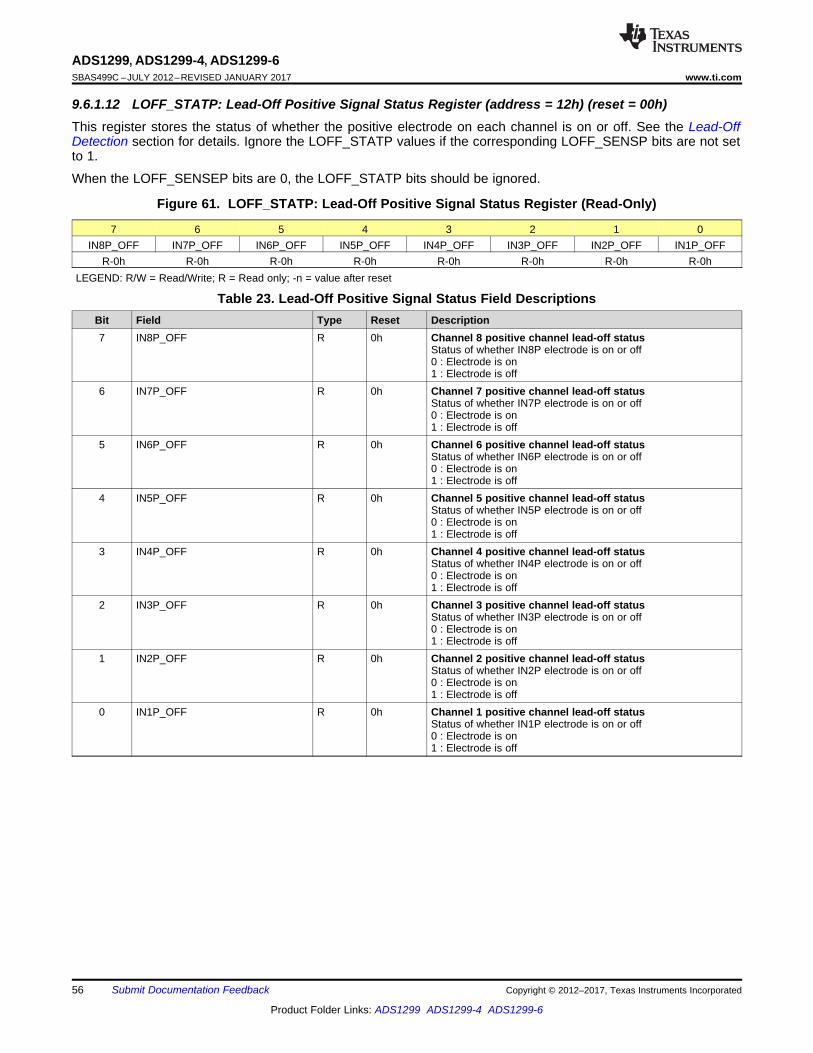
56
ADS1299, ADS1299-4, ADS1299-6SBAS499C –JULY 2012–REVISED JANUARY 2017 www.ti.com
Product Folder Links: ADS1299 ADS1299-4 ADS1299-6
Submit Documentation Feedback Copyright © 2012–2017, Texas Instruments Incorporated
9.6.1.12 LOFF_STATP: Lead-Off Positive Signal Status Register (address = 12h) (reset = 00h)This register stores the status of whether the positive electrode on each channel is on or off. See the Lead-OffDetection section for details. Ignore the LOFF_STATP values if the corresponding LOFF_SENSP bits are not setto 1.
When the LOFF_SENSEP bits are 0, the LOFF_STATP bits should be ignored.
Figure 61. LOFF_STATP: Lead-Off Positive Signal Status Register (Read-Only)
7 6 5 4 3 2 1 0IN8P_OFF IN7P_OFF IN6P_OFF IN5P_OFF IN4P_OFF IN3P_OFF IN2P_OFF IN1P_OFF
R-0h R-0h R-0h R-0h R-0h R-0h R-0h R-0hLEGEND: R/W = Read/Write; R = Read only; -n = value after reset
Table 23. Lead-Off Positive Signal Status Field DescriptionsBit Field Type Reset Description7 IN8P_OFF R 0h Channel 8 positive channel lead-off status
Status of whether IN8P electrode is on or off0 : Electrode is on1 : Electrode is off
6 IN7P_OFF R 0h Channel 7 positive channel lead-off statusStatus of whether IN7P electrode is on or off0 : Electrode is on1 : Electrode is off
5 IN6P_OFF R 0h Channel 6 positive channel lead-off statusStatus of whether IN6P electrode is on or off0 : Electrode is on1 : Electrode is off
4 IN5P_OFF R 0h Channel 5 positive channel lead-off statusStatus of whether IN5P electrode is on or off0 : Electrode is on1 : Electrode is off
3 IN4P_OFF R 0h Channel 4 positive channel lead-off statusStatus of whether IN4P electrode is on or off0 : Electrode is on1 : Electrode is off
2 IN3P_OFF R 0h Channel 3 positive channel lead-off statusStatus of whether IN3P electrode is on or off0 : Electrode is on1 : Electrode is off
1 IN2P_OFF R 0h Channel 2 positive channel lead-off statusStatus of whether IN2P electrode is on or off0 : Electrode is on1 : Electrode is off
0 IN1P_OFF R 0h Channel 1 positive channel lead-off statusStatus of whether IN1P electrode is on or off0 : Electrode is on1 : Electrode is off

57
ADS1299, ADS1299-4, ADS1299-6www.ti.com SBAS499C –JULY 2012–REVISED JANUARY 2017
Product Folder Links: ADS1299 ADS1299-4 ADS1299-6
Submit Documentation FeedbackCopyright © 2012–2017, Texas Instruments Incorporated
9.6.1.13 LOFF_STATN: Lead-Off Negative Signal Status Register (address = 13h) (reset = 00h)This register stores the status of whether the negative electrode on each channel is on or off. See the Lead-OffDetection section for details. Ignore the LOFF_STATN values if the corresponding LOFF_SENSN bits are not setto 1.
When the LOFF_SENSEN bits are 0, the LOFF_STATP bits should be ignored.
Figure 62. LOFF_STATN: Lead-Off Negative Signal Status Register (Read-Only)
7 6 5 4 3 2 1 0IN8N_OFF IN7N_OFF IN6N_OFF IN5N_OFF IN4N_OFF IN3N_OFF IN2N_OFF IN1N_OFF
R-0h R-0h R-0h R-0h R-0h R-0h R-0h R-0hLEGEND: R/W = Read/Write; R = Read only; -n = value after reset
Table 24. Lead-Off Negative Signal Status Field DescriptionsBit Field Type Reset Description7 IN8N_OFF R 0h Channel 8 negative channel lead-off status
Status of whether IN8N electrode is on or off0 : Electrode is on1 : Electrode is off
6 IN7N_OFF R 0h Channel 7 negative channel lead-off statusStatus of whether IN7N electrode is on or off0 : Electrode is on1 : Electrode is off
5 IN6N_OFF R 0h Channel 6 negative channel lead-off statusStatus of whether IN6N electrode is on or off0 : Electrode is on1 : Electrode is off
4 IN5N_OFF R 0h Channel 5 negative channel lead-off statusStatus of whether IN5N electrode is on or off0 : Electrode is on1 : Electrode is off
3 IN4N_OFF R 0h Channel 4 negative channel lead-off statusStatus of whether IN4N electrode is on or off0 : Electrode is on1 : Electrode is off
2 IN3N_OFF R 0h Channel 3 negative channel lead-off statusStatus of whether IN3N electrode is on or off0 : Electrode is on1 : Electrode is off
1 IN2N_OFF R 0h Channel 2 negative channel lead-off statusStatus of whether IN2N electrode is on or off0 : Electrode is on1 : Electrode is off
0 IN1N_OFF R 0h Channel 1 negative channel lead-off statusStatus of whether IN1N electrode is on or off0 : Electrode is on1 : Electrode is off

58
ADS1299, ADS1299-4, ADS1299-6SBAS499C –JULY 2012–REVISED JANUARY 2017 www.ti.com
Product Folder Links: ADS1299 ADS1299-4 ADS1299-6
Submit Documentation Feedback Copyright © 2012–2017, Texas Instruments Incorporated
9.6.1.14 GPIO: General-Purpose I/O Register (address = 14h) (reset = 0Fh)The general-purpose I/O register controls the action of the three GPIO pins. When RESP_CTRL[1:0] is in mode01 and 11, the GPIO2, GPIO3, and GPIO4 pins are not available for use.
Figure 63. GPIO: General-Purpose I/O Register
7 6 5 4 3 2 1 0GPIOD[4:1] GPIOC[4:1]
R/W-0h R/W-FhLEGEND: R/W = Read/Write; R = Read only; -n = value after reset
Table 25. General-Purpose I/O Field DescriptionsBit Field Type Reset Description7:4 GPIOD[4:1] R/W 0h GPIO data
These bits are used to read and write data to the GPIO ports.When reading the register, the data returned correspond to thestate of the GPIO external pins, whether they are programmedas inputs or as outputs. As outputs, a write to the GPIOD setsthe output value. As inputs, a write to the GPIOD has no effect.GPIO is not available in certain respiration modes.
3:0 GPIOC[4:1] R/W Fh GPIO control (corresponding GPIOD)These bits determine if the corresponding GPIOD pin is an inputor output.0 : Output1 : Input

59
ADS1299, ADS1299-4, ADS1299-6www.ti.com SBAS499C –JULY 2012–REVISED JANUARY 2017
Product Folder Links: ADS1299 ADS1299-4 ADS1299-6
Submit Documentation FeedbackCopyright © 2012–2017, Texas Instruments Incorporated
9.6.1.15 MISC1: Miscellaneous 1 Register (address = 15h) (reset = 00h)This register provides the control to route the SRB1 pin to all inverting inputs of the four, six, or eight channels(ADS1299-4, ADS1299-6, or ADS1299).
Figure 64. MISC1: Miscellaneous 1 Register
7 6 5 4 3 2 1 00 0 SRB1 0 0 0 0 0
R/W-0h R/W-0h R/W-0h R/W-0h R/W-0h R/W-0h R/W-0h R/W-0hLEGEND: R/W = Read/Write; R = Read only; -n = value after reset
Table 26. Miscellaneous 1 Register Field DescriptionsBit Field Type Reset Description7:6 Reserved R/W 0h Reserved
Always write 0h5 SRB1 R/W 0h Stimulus, reference, and bias 1
This bit connects the SRB1 to all 4, 6, or 8 channels invertinginputs0 : Switches open1 : Switches closed
4:0 Reserved R/W 0h ReservedAlways write 0h
9.6.1.16 MISC2: Miscellaneous 2 (address = 16h) (reset = 00h)This register is reserved for future use.
Figure 65. MISC1: Miscellaneous 1 Register
7 6 5 4 3 2 1 00 0 0 0 0 0 0 0
R/W-0h R/W-0h R/W-0h R/W-0h R/W-0h R/W-0h R/W-0h R/W-0hLEGEND: R/W = Read/Write; R = Read only; -n = value after reset
Table 27. Miscellaneous 1 Register Field DescriptionsBit Field Type Reset Description7:0 Reserved R/W 0h Reserved
Always write 0h

60
ADS1299, ADS1299-4, ADS1299-6SBAS499C –JULY 2012–REVISED JANUARY 2017 www.ti.com
Product Folder Links: ADS1299 ADS1299-4 ADS1299-6
Submit Documentation Feedback Copyright © 2012–2017, Texas Instruments Incorporated
9.6.1.17 CONFIG4: Configuration Register 4 (address = 17h) (reset = 00h)This register configures the conversion mode and enables the lead-off comparators.
Figure 66. CONFIG4: Configuration Register 4
7 6 5 4 3 2 1 0
0 0 0 0 SINGLE_SHOT 0 PD_LOFF_COMP 0
R/W-0h R/W-0h R/W-0h R/W-0h R/W-0h R/W-0h R/W-0h R/W-0hLEGEND: R/W = Read/Write; R = Read only; -n = value after reset
Table 28. Configuration Register 4 Field DescriptionsBit Field Type Reset Description7:4 Reserved R/W 0h Reserved
Always write 0h3 SINGLE_SHOT R/W 0h Single-shot conversion
This bit sets the conversion mode.0 : Continuous conversion mode1 : Single-shot mode
2 Reserved R/W 0h ReservedAlways write 0h
1 PD_LOFF_COMP R/W 0h Lead-off comparator power-downThis bit powers down the lead-off comparators.0 : Lead-off comparators disabled1 : Lead-off comparators enabled
0 Reserved R/W 0h ReservedAlways write 0h

61
ADS1299, ADS1299-4, ADS1299-6www.ti.com SBAS499C –JULY 2012–REVISED JANUARY 2017
Product Folder Links: ADS1299 ADS1299-4 ADS1299-6
Submit Documentation FeedbackCopyright © 2012–2017, Texas Instruments Incorporated
10 Applications and Implementation
NOTEInformation in the following applications sections is not part of the TI componentspecification, and TI does not warrant its accuracy or completeness. TI’s customers areresponsible for determining suitability of components for their purposes. Customers shouldvalidate and test their design implementation to confirm system functionality.
10.1 Application Information
10.1.1 Unused Inputs and OutputsPower down unused analog inputs and connect them directly to AVDD.
Power down the Bias amplifier if unused and float BIASOUT and BIASINV. BIASIN can also float or can be tieddirectly to AVSS if unused.
Tie BIASREF directly to AVSS or leave floating if unused.
Tie SRB1 and SRB2 directly to AVSS or leave them floating if unused.
Do not float unused digital inputs because excessive power-supply leakage current might result. Set the two-state mode setting pins high to DVDD or low to DGND through ≥10-kΩ resistors.
Pull DRDY to supply using weak pullup resistor if unused.
If not daisy-chaining devices, tie DAISYIN directly to DGND.
10.1.2 Setting the Device for Basic Data CaptureFigure 67 outlines the procedure to configure the device in a basic state and capture data. This procedure putsthe device into a configuration that matches the parameters listed in the specifications section, in order to checkif the device is working properly in the user system. Follow this procedure initially until familiar with the devicesettings. After this procedure has been verified, the device can be configured as needed. For details on thetimings for commands, see the appropriate sections in the data sheet. Sample programming codes are added forthe ECG and EEG-specific functions.
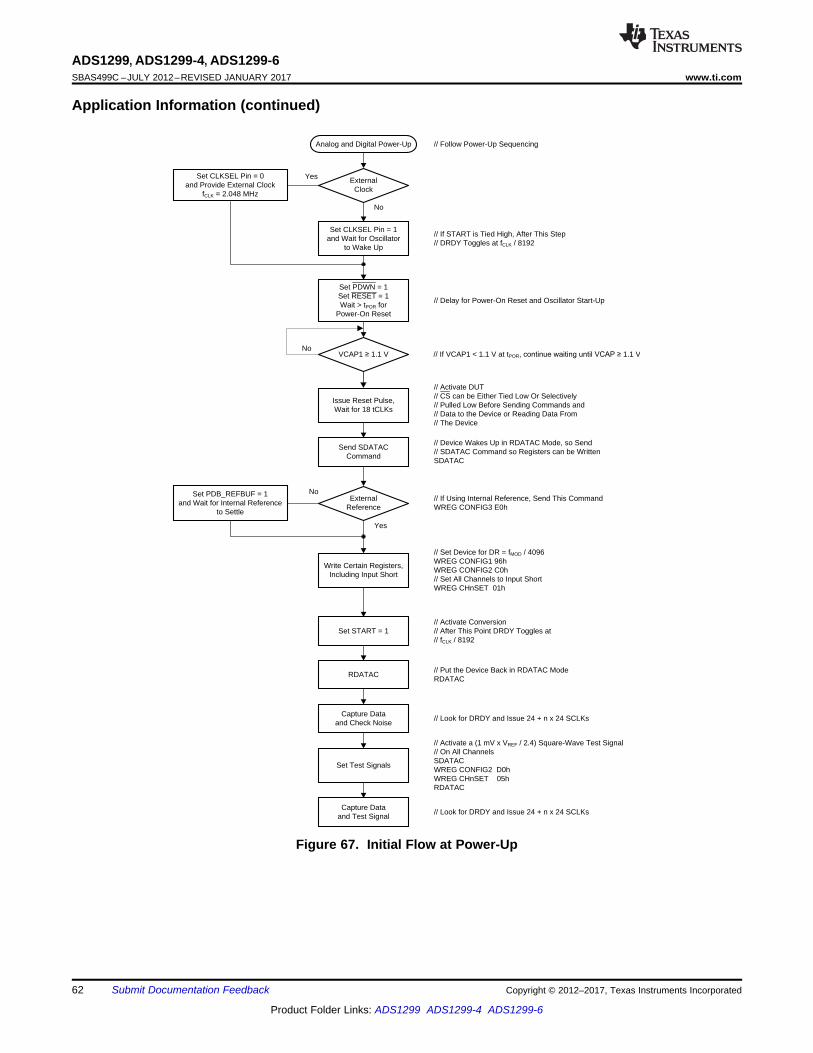
Set PDWN = 1Set RESET = 1Wait > tPOR for
Power-On Reset
// Delay for Power-On Reset and Oscillator Start-Up
// If START is Tied High, After This Step// DRDY Toggles at fCLK / 8192
Set CLKSEL Pin = 1and Wait for Oscillator
to Wake Up
No
// Follow Power-Up Sequencing
ExternalClock
Set CLKSEL Pin = 0and Provide External Clock
fCLK = 2.048 MHz
Yes
Set PDB_REFBUF = 1and Wait for Internal Reference
to Settle
Write Certain Registers,Including Input Short
Set START = 1// Activate Conversion// After This Point DRDY Toggles at// fCLK / 8192
// Set Device for DR = fMOD / 4096WREG CONFIG1 96hWREG CONFIG2 C0h// Set All Channels to Input ShortWREG CHnSET 01h
Yes
RDATAC// Put the Device Back in RDATAC ModeRDATAC
Capture Dataand Check Noise
// Look for DRDY and Issue 24 + n x 24 SCLKs
Set Test Signals
Capture Dataand Test Signal
// Activate a (1 mV x VREF / 2.4) Square-Wave Test Signal// On All ChannelsSDATACWREG CONFIG2 D0hWREG CHnSET 05hRDATAC
ExternalReference
// If Using Internal Reference, Send This CommandWREG CONFIG3 E0h
No
Send SDATACCommand
// Device Wakes Up in RDATAC Mode, so Send// SDATAC Command so Registers can be WrittenSDATAC
Issue Reset Pulse,Wait for 18 tCLKs
// Activate DUT// CS can be Either Tied Low Or Selectively // Pulled Low Before Sending Commands and// Data to the Device or Reading Data From// The Device
Analog and Digital Power-Up
// Look for DRDY and Issue 24 + n x 24 SCLKs
VCAP1 1.1 VNo
// If VCAP1 < 1.1 V at tPOR, FRQWLQXHZDLWLQJXQWLO9&$31.1 V
62
ADS1299, ADS1299-4, ADS1299-6SBAS499C –JULY 2012–REVISED JANUARY 2017 www.ti.com
Product Folder Links: ADS1299 ADS1299-4 ADS1299-6
Submit Documentation Feedback Copyright © 2012–2017, Texas Instruments Incorporated
Application Information (continued)
Figure 67. Initial Flow at Power-Up

INxP
INxN
BIASOUT
BIASINV
1 M
TI Device
1.5 nF
Antialiasing, Protection
Antialiasing, Protection
Protection
Electrode 1
Electrode 2
BIAS Electrode
Copyright © 2016, Texas Instruments Incorporated
63
ADS1299, ADS1299-4, ADS1299-6www.ti.com SBAS499C –JULY 2012–REVISED JANUARY 2017
Product Folder Links: ADS1299 ADS1299-4 ADS1299-6
Submit Documentation FeedbackCopyright © 2012–2017, Texas Instruments Incorporated
Application Information (continued)10.1.2.1 Lead-OffSample code to set dc lead-off with pull-up and pull-down resistors on all channels.
WREG LOFF 0x13 // Comparator threshold at 95% and 5%, pullup or pulldown resistor// dc lead-off
WREG CONFIG4 0x02 // Turn on dc lead-off comparatorsWREG LOFF_SENSP 0xFF // Turn on the P-side of all channels for lead-off sensingWREG LOFF_SENSN 0xFF // Turn on the N-side of all channels for lead-off sensing
Observe the status bits of the output data stream to monitor lead-off status.
10.1.2.2 Bias DriveSample code to choose bias as an average of the first three channels.
WREG RLD_SENSP 0x07 // Select channel 1-3 P-side for RLD sensingWREG RLD_SENSN 0x07 // Select channel 1-3 N-side for RLD sensingWREG CONFIG3 b’x1xx 1100 // Turn on BIAS amplifier, set internal BIASREF voltage
Sample code to route the BIASOUT signal through channel 4 N-side and measure bias with channel 5. Makesure the external side to the chip BIASOUT is connected to BIASIN.
WREG CONFIG3 b’xxx1 1100 // Turn on BIAS amp, set internal BIASREF voltage, set BIAS measurement bitWREG CH4SET b’xxxx 0111 // Route BIASIN to channel 4 N-sideWREG CH5SET b’xxxx 0010 // Route BIASIN to be measured at channel 5 w.r.t BIASREF
10.1.3 Establishing the Input Common-ModeThe ADS1299-x measures fully-differential signals where the common-mode voltage point is the midpoint of thepositive and negative analog input. The internal PGA restricts the common-mode input range because of theheadroom required for operation. The human body is prone to common-mode drifts because noise easily couplesonto the human body, similar to an antenna. These common-mode drifts may push the ADS1299-x inputcommon-mode voltage out of the measurable range of the ADC.
If a patient-drive electrode is used by the system, the ADS1299-x includes an on-chip bias drive (BIAS) amplifierthat connects to the patient drive electrode. The BIAS amplifier function is to bias the patient to maintain theother electrode common-mode voltages within the valid range. When powered on, the amplifier uses either theanalog midsupply voltage, or the voltage present at the BIASREF pin, as a reference input to drive the patient tothat voltage.
The ADS1299-x provides the option to use input electrode voltages as feedback to the amplifier to moreeffectively stabilize the output to the amplifier reference voltage by setting corresponding bits in theBIAS_SENSP and BIAS_SENSN registers. Figure 68 shows an example of a three-electrode system thatleverages this technique.
Figure 68. Setting Common-Mode Using BIAS Electrode

START1
Device 1
CLK
DRDY DRDY1
START
CLK
START2
Device 2
CLK
DRDY DRDY2
START
CLK
DRDY1
DRDY2
64
ADS1299, ADS1299-4, ADS1299-6SBAS499C –JULY 2012–REVISED JANUARY 2017 www.ti.com
Product Folder Links: ADS1299 ADS1299-4 ADS1299-6
Submit Documentation Feedback Copyright © 2012–2017, Texas Instruments Incorporated
Application Information (continued)10.1.4 Multiple Device ConfigurationThe ADS1299-x is designed to provide configuration flexibility when multiple devices are used in a system. Theserial interface typically needs four signals: DIN, DOUT, SCLK, and CS. With one additional chip select signalper device, multiple devices can be connected together. The number of signals needed to interface n devices is3 + n.
The BIAS drive amplifiers can be daisy-chained, as explained in the Bias Configuration with Multiple Devicessection. To use the internal oscillator in a daisy-chain configuration, one device must be set as the master for theclock source with the internal oscillator enabled (CLKSEL pin = 1) and the internal oscillator clock brought out ofthe device by setting the CLK_EN register bit to '1'. This master device clock is used as the external clock sourcefor other devices.
When using multiple devices, the devices can be synchronized with the START signal. The delay from START tothe DRDY signal is fixed for a given data rate (see the Start subsection of the SPI Interface section for moredetails on the settling times). Figure 69 shows the behavior of two devices when synchronized with the STARTsignal.
There are two ways to connect multiple devices with a optimal number of interface pins: cascade mode anddaisy-chain mode.
Figure 69. Synchronizing Multiple Converters
10.1.4.1 Cascaded ModeFigure 70a illustrates a configuration with two devices cascaded together. Together, the devices create a systemwith 16 channels. DOUT, SCLK, and DIN are shared. Each device has its own chip select. When a device is notselected by the corresponding CS being driven to logic 1, the DOUT of this device is high-impedance. Thisstructure allows the other device to take control of the DOUT bus. This configuration method is suitable for themajority of applications.

DOUT
DAISY_IN1
0
DO TU 0
SCLK
MSB1
MSB0
21 3 216 217 218
MSB1LSB0
LSB1
219 337
LSB1
Da a Ft rom D ce 1evi Da a Ft rom viDe ce 2
START DRDY
CS
SCLK
DIN
DOUT
Device 1
START DRDY
CS
SCLK
DIN
DOUTDevice 2
START(1)
a) Standard Configuration
CLK
CLK
INT
GPO0
GPO1
SCLK
MOSI
Host Processor
MISO
CLK
START DRDY
CS
SCLK
DIN
DOUT0
Device 1
START
DRDY
CS
SCLK
DIN
DAISY_IN1
Device 2
START(1)
b) Daisy-Chain Configuration
CLK
CLK
INT
GPO
SCLK
MOSI
Host Processor
MISO
CLK
0
DOUT1
DAISY_IN0
65
ADS1299, ADS1299-4, ADS1299-6www.ti.com SBAS499C –JULY 2012–REVISED JANUARY 2017
Product Folder Links: ADS1299 ADS1299-4 ADS1299-6
Submit Documentation FeedbackCopyright © 2012–2017, Texas Instruments Incorporated
Application Information (continued)10.1.4.2 Daisy-Chain ModeDaisy-chain mode is enabled by setting the DAISY_EN bit in the CONFIG1 register. Figure 70b shows the daisy-chain configuration. In this mode SCLK, DIN, and CS are shared across multiple devices. The DOUT of thesecond device is connected to the DAISY_IN of the first device, thereby creating a chain. When using daisy-chain mode, the multiple readback feature is not available. Short the DAISY_IN pin to digital ground if not used.Figure 2 describes the required timing for the device shown in the configurations of Figure 70. Status and datafrom device 1 appear first on DOUT, followed by the status and data from device 2. The ADS1299 can be daisychained with a second ADS1299, an ADS1299-6, or an ADS1299-4.
(1) To reduce pin count, set the START pin low and use the START serial command to synchronize and startconversions.
Figure 70. Multiple Device Configurations
When all devices in the chain operate in the same register setting, DIN can be shared as well. This configurationreduces the SPI communication signals to four, regardless of the number of devices. The BIAS driver cannot beshared among the multiple devices and an external clock must be used because the individual devices cannot beprogrammed when sharing a common DIN.
Note that from Figure 2, the SCLK rising edge shifts data out of the device on DOUT. The SCLK negative edgeis used to latch data into the device DAISY_IN pin down the chain. This architecture allows for a faster SCLKrate speed, but also makes the interface sensitive to board-level signal delays. The more devices in the chain,the more challenging adhering to setup and hold times becomes. A star-pattern connection of SCLK to alldevices, minimizing DOUT length, and other printed circuit board (PCB) layout techniques helps. Placing delaycircuits (such as buffers) between DOUT and DAISY_IN are ways to mitigate this challenge. One other option isto insert a D flip-flop between DOUT and DAISY_IN clocked on an inverted SCLK. Note also that daisy-chainmode requires some software overhead to recombine data bits spread across byte boundaries. Figure 71 showsa timing diagram for this mode.
Figure 71. Daisy-Chain Timing

.
.
.
IN1P
IN1N
BIASINV
BIASOUT
Electrode 1
Electrode 2
Bias Electrode
.
.
.
IN2P
IN2N
Electrode 3
Electrode 4
AVDD
AVSS
+2.5 V
-2.5 V
+ADC
+
+ADC
.
.
.
. . .
(AVDD + AVSS)/2BIASREF_INT
BIASP1 BIASN1 BIASP2 BIASN2
RFilt
RFilt
RFilt
RFilt
CFilt
CFilt
CFRF
RP
220 k 220 k 220 k 220 k
fSCLK
f (N )(NDR BITS CHANNELS) + 24N =DEVICES
66
ADS1299, ADS1299-4, ADS1299-6SBAS499C –JULY 2012–REVISED JANUARY 2017 www.ti.com
Product Folder Links: ADS1299 ADS1299-4 ADS1299-6
Submit Documentation Feedback Copyright © 2012–2017, Texas Instruments Incorporated
Application Information (continued)The maximum number of devices that can be daisy-chained depends on the data rate at which the device isoperated at. The maximum number of devices can be approximately calculated with Equation 10.
where:NBITS = device resolution (depending on data rate), andNCHANNELS = number of channels in the device. (10)
For example, when the 8-channel ADS1299 is operated at a 2-kSPS data rate with a 4-MHz fSCLK, 10 devicescan be daisy-chained.
10.2 Typical ApplicationThe biopotential signals that are measured in electroencephalography (EEG) are small when compared to othertypes of biopotential signals. The ADS1299 is equipped to measure such small signals due to its extremely lowinput-referred noise from its high performance internal PGA. Figure 72 and Figure 73 are examples of how theADS1299 may be configured in typical EEG measurement setups. Figure 72 shows how to measure electrodepotentials in a sequential montage, whereas Figure 73 illustrates referential montage measurement connections.
Figure 72. Example Schematic Using the ADS1299 in an EEG Data Acquisition Application, SequentialMontage

.
.
.
IN1P
IN2P
BIASINV
BIASOUT
Electrode 1
Electrode 2
Bias Electrode
IN3P
IN4P
Electrode 3
Electrode 4
AVDD
AVSS
+2.5 V
-2.5 V
SRB1ReferenceElectrode
+ADC
+
+ADC
.
.
.
. . .
(AVDD + AVSS)/2BIASREF_INT
BIASP1 BIASN1 BIASP2 BIASN2
220 k 220 k 220 k 220 k
+ADC
+ADC
.
.
.SRB1
BIASP3 BIASN3 BIASP4 BIASN4
220 k 220 k 220 k 220 k
RFilt
RFilt
RFilt
RFilt
RFilt
CFilt CFilt CFilt CFilt
CFRF
RP
67
ADS1299, ADS1299-4, ADS1299-6www.ti.com SBAS499C –JULY 2012–REVISED JANUARY 2017
Product Folder Links: ADS1299 ADS1299-4 ADS1299-6
Submit Documentation FeedbackCopyright © 2012–2017, Texas Instruments Incorporated
Typical Application (continued)
Figure 73. Example Schematic Using the ADS1299 in an EEG Data Acquisition Application, ReferentialMontage
10.2.1 Design RequirementsTable 29 shows the design requirements for a typical EEG measurement system.
Table 29. EEG Data Acquisition Design RequirementsDESIGN PARAMETER VALUE
Bandwidth 1 Hz - 50 HzMinimum signal bandwidth 10 μVPk
Input Impedance > 10 MΩ
Coupling dc
10.2.2 Detailed Design ProcedureEach channel on the ADS1299 is optimized to measure a separate EEG waveform. The specific connectionsdepend on the EEG montage. The sequential montage is a configuration where each channel represents thevoltage between two adjacent electrodes. For example, to measure the potential between electrode Fp1 and F7on channel 1 of the ADS1299, route the Fp1 electrode to IN1P and the F7 electrode to IN1N. The connectionsfor a sequential montage are illustrated in Figure 72.

out f
in
V R N
V 330k
u
:
68
ADS1299, ADS1299-4, ADS1299-6SBAS499C –JULY 2012–REVISED JANUARY 2017 www.ti.com
Product Folder Links: ADS1299 ADS1299-4 ADS1299-6
Submit Documentation Feedback Copyright © 2012–2017, Texas Instruments Incorporated
Alternatively, EEG electrodes can be measured in a referential montage in which each of the electrodes ismeasured with respect to a single reference electrode. This montage also allows calculation of the waveformsthat would have been measured in a sequential montage by finding the difference between two electrodewaveforms which were measured with respect to the same electrode. The ADS1299 allows for such aconfiguration through the use of the SRB1 pin. The SRB1 pin on the ADS1299 may be internally routed to eachchannel negative input by setting the SRB1 bit in the MISC1 register. When the reference electrode is connectedto the SRB1 pin and all other electrodes are connected to the respective positive channel inputs, the electrodevoltages can be measured with a referential montage. The referential montage is illustrated in Figure 73. SeeFigure 18 for a diagram of the channel input multiplexer options.
The ADS1299 is designed to be an EEG front end such that no additional amplification or buffer stage is neededbetween the electrodes and ADS1299. The ADS1299 has a low-noise PGA with excellent input-referred noiseperformance. For certain data rate and gain settings, the ADS1299 introduces significantly less than 1 μVRMS ofinput-referred noise to the signal chain making the device more than capable of handling the 10-μVPk minimumsignal amplitude. ADS1299 noise performance for different PGA gains and data rate settings is listed in Table 1,Table 2, Table 3, and Table 4.
Traditional EEG data acquisition systems high-pass filter the signals in the front-end to remove dc signal content.This topology allows the signal to be amplified by a large gain so the signal can be digitized by a 12- to 16-bitADC. The ADS1299 24-bit resolution allows the signal to be dc-coupled to the ADC because small EEG signalinformation can be measured in addition to a significant dc offset.
The ADS1299 channel inputs have very low input bias current allowing electrodes to be connected to the inputsof the ADS1299 with very little leakage current flowing on the patient cables. The ADS1299 has a minimum dcinput impedance of 1 GΩ when the lead-off current sources are disabled and 500 MΩ typically when the lead-offcurrent sources are enabled.
The passive components RFilt and CFilt form low-pass filters. In general, the filter is advised to be formed by usinga differential capacitor CFIlt that shunts the inputs rather than individual RC filters whose capacitors shunt toground. The differential capacitor configuration significantly improves common-mode rejection because thisapproach removes dependence on component mismatch.
The cutoff frequency for the filter can be placed well past the data rate of the ADC because of the delta-sigmaADC filter-then-decimate topology. Take care to prevent aliasing around the first repetition of the digitaldecimation filter response at fMOD. Assuming a 2.048-MHz fCLK, fMOD = 1.024 MHz. The value of RFilt has aminimum set by technical standards for medical electronics. The capacitor value must be set to arrange theproper cutoff frequency.
If the system is likely to be exposed to high-frequency EMI, adding very small-value, common-mode capacitors tothe inputs is advisable to filter high-frequency common-mode signals. If these capacitors are added, then thecapacitors should be 10 or 20 times smaller than the differential capacitor to ensure their effect of CMRR isminimized.
The integrated bias amplifier serves two purposes in an EEG data acquisition system with the ADS1299. Thebias amplifier provides a bias voltage that, when applied to the patient, keeps the measurement electrodecommon-mode voltage within the rails of the ADS1299. This scenario allows for dc coupling. In addition, the biasamplifier can be configured to provide negative common-mode feedback to the patient to cancel unwantedcommon-mode signals appearing on the electrodes. This feature is especially helpful because biopotentialacquisition systems are notoriously prone to mains-frequency common-mode interference.
The bias amplifier is powered on by setting the PD_BIAS bit in the CONFIG3 register. Set the BIASREF_INT bitin the CONFIG3 register to input the internally generated analog mid-supply voltage the noninverting input of thebias amplifier. To enable an electrode as an input to the bias amplifier, set the corresponding bit in theBIAS_SENSP or BIAS_SENSN register.
The dc gain of the bias amplifier is determined by RBias and the number of channel inputs enabled as inputs tothe bias amplifier. The bias amplifier circuit only passes common-mode signals. Therefore, the 330-kΩ resistorsat each PGA output are in parallel for common-mode signals. The bias amplifier is configured in an inverting gainscheme. The formula for determining dc gain for common-mode signals input to the bias amplifier is shown inEquation 11. The capacitor Cf sets the bandwidth for the bias amplifier. Ensure that the amplifier has enoughbandwidth to output all the intended common-mode signals.
(11)
Time (s)
Vol
tage
(P
V)
0 0.1 0.2 0.3 0.4 0.5 0.6 0.7 0.8 0.9 1-4.5
-3.5
-2.5
-1.5
-0.5
0.5
1.5
2.5
3.5
4.5
D001
INxP
INxN
AVDD
+2.5 V
AVSS
-2.5 V
4.99 k
4.7 nF
952 k
10.3 k 33 VRMS
10 Hz
69
ADS1299, ADS1299-4, ADS1299-6www.ti.com SBAS499C –JULY 2012–REVISED JANUARY 2017
Product Folder Links: ADS1299 ADS1299-4 ADS1299-6
Submit Documentation FeedbackCopyright © 2012–2017, Texas Instruments Incorporated
Another advantage to a dc-coupled EEG data acquisition system is the ability to detect when an electrode nolonger makes good contact with the patient. The ADS1299 features integrated lead-off detection electronics. TheLead-Off Detection section explains how to use the lead-off feature on the ADS1299. Note that when configuredin a referential montage, only use one lead-off current source with the reference electrode.
10.2.3 Application CurvesTesting the capability of the ADS1299 to measure signals in the band and near the amplitude of typical EEGsignals can be done with a precision signal generator. The ADS1299 was tested in a configuration like the oneshown in Figure 74.
Figure 74. Example Schematic Using the ADS1299 in an EEG Data Acquisition Application, ReferentialMontage
The 952-kΩ and 10.3-kΩ resistors were used to attenuate the voltage from the signal source because the sourcecould not reach the desired magnitude directly. With the voltage divider, the signal appearing at the inputs was a3.5-μVRMS, 10-Hz sine wave. Figure 75 shows the input-referred conversion results from the ADS1299 followingcalibration for offset. The signal that is measured is similar to some of the smallest extracranial EEG signals thatcan be measured with typical EEG acquisition systems. The signal can be clearly identified. Given thismeasurement setup was a single-ended configuration without shielding, the measurement setup was subject tosignificant mains interference. A digital low-pass filter was applied to remove the interference.
Figure 75. ADS1299 10-Hz Input Signal Results

VCAP1
Supplies
tPOR(1)(2)
VCAP = 1.1V
1.1V
tBG(1)
tRST
18 × tCLK
Start using device
RESET
70
ADS1299, ADS1299-4, ADS1299-6SBAS499C –JULY 2012–REVISED JANUARY 2017 www.ti.com
Product Folder Links: ADS1299 ADS1299-4 ADS1299-6
Submit Documentation Feedback Copyright © 2012–2017, Texas Instruments Incorporated
11 Power Supply RecommendationsThe ADS1299-x has three power supplies: AVDD, AVDD1, and DVDD. For best performance, both AVDD andAVDD1 must be as quiet as possible. AVDD1 provides the supply to the charge pump block and has transientsat fCLK. Therefore, star connect AVDD1 to the AVDD pins and AVSS1 to the AVSS pins. AVDD and AVDD1noise that is nonsynchronous with the ADS1299-x operation must be eliminated. Bypass each device supply with10-μF and 0.1-μF solid ceramic capacitors. For best performance, place the digital circuits (DSP,microcontrollers, FPGAs, and so forth) in the system so that the return currents on those devices do not crossthe analog return path of the device. Power the ADS1299-x from unipolar or bipolar supplies.
Use surface-mount, low-cost, low-profile, multilayer ceramic-type capacitors for decoupling. In most cases, theVCAP1 capacitor is also a multilayer ceramic; however, in systems where the board is subjected to high- or low-frequency vibration, install a nonferroelectric capacitor, such as a tantalum or class 1 capacitor (C0G or NPO).EIA class 2 and class 3 dielectrics such as (X7R, X5R, X8R, and so forth) are ferroelectric. The piezoelectricproperty of these capacitors can appear as electrical noise coming from the capacitor. When using internalreference, noise on the VCAP1 node results in performance degradation.
11.1 Power-Up SequencingBefore device power up, all digital and analog inputs must be low. At the time of power up, keep all of thesesignals low until the power supplies have stabilized, as shown in Figure 76.
Allow time for the supply voltages to reach their final value, and then begin supplying the master clock signal tothe CLK pin. Wait for time tPOR, then transmit a reset pulse using either the RESET pin or RESET command toinitialize the digital portion of the chip. Issue the reset after tPOR or after the VCAP1 voltage is greater than 1.1 V,whichever time is longer. Note that:• tPOR is described in Table 30.• The VCAP1 pin charge time is set by the RC time constant set by the capacitor value on VCAP1; see
Figure 25.
After releasing the RESET pin, program the configuration registers. The power-up sequence timing is shown inTable 30.
(1) Timing to reset pulse is tPOR or after tBG, whichever is longer.(2) When using an external clock, tPOR timing does not start until CLK is present and valid.
Figure 76. Power-Up Timing Diagram
Table 30. Timing Requirements for Figure 76MIN MAX UNIT
tPOR Wait after power up until reset 218 tCLK
tRST Reset low duration 2 tCLK
11.2 Connecting the Device to Unipolar (5 V and 3.3 V) SuppliesFigure 77 illustrates the ADS1299-x connected to a unipolar supply. In this example, analog supply (AVDD) isreferenced to analog ground (AVSS) and digital supply (DVDD) is referenced to digital ground (DGND).

Device
0.1 Fm1 Fm
AVDD AVDD1
0.1 Fm1 Fm
-2.5 V
AVSSAVSS1 DGND
DVDD
+2.5 V
+3.3 V
0.1 Fm 1 Fm
VCAP1
VCAP2
VCAP3
0.1 Fm
VREFP
VREFN10 Fm
VCAP4
1 Fm 1 Fm1 Fm
-2.5 V
100 Fm0.1 Fm
RESV1
Device
AVDD
0.1 Fm1 Fm
+5 V
AVDD1
AVSSAVSS1 DGND
DVDD
+3.3 V
0.1 Fm 1 Fm
0.1 Fm
VREFP
VREFN
VCAP1
VCAP2
VCAP3
VCAP4
1 Fm 1 Fm 1 Fm
10 Fm
100 Fm0.1 Fm
RESV1
71
ADS1299, ADS1299-4, ADS1299-6www.ti.com SBAS499C –JULY 2012–REVISED JANUARY 2017
Product Folder Links: ADS1299 ADS1299-4 ADS1299-6
Submit Documentation FeedbackCopyright © 2012–2017, Texas Instruments Incorporated
Connecting the Device to Unipolar (5 V and 3.3 V) Supplies (continued)
NOTE: Place the capacitors for supply, reference, and VCAP1 to VCAP4 as close to the package as possible.
Figure 77. Single-Supply Operation
11.3 Connecting the Device to Bipolar (±2.5 V and 3.3 V) SuppliesFigure 78 shows the ADS1299-x connected to a bipolar supply. In this example, the analog supplies connect tothe device analog supply (AVDD). This supply is referenced to the device analog return (AVSS), and the digitalsupply (DVDD) is referenced to the device digital ground return (DGND).
NOTE: Place the capacitors for supply, reference, and VCAP1 to VCAP4 as close to the package as possible.
Figure 78. Bipolar Supply Operation

Device Microcontroller
Signal
Conditioning
(RC Filters
and
Amplifiers)
Supply
Generation
Connector
or Antenna
Ground Fill orGround Plane
Optional: S
plit
Gro
und
CutGround Fill or
Ground Plane
Optional: S
plit
Gro
und C
ut
InterfaceTransceiver
Ground Fill orGround Plane
Ground Fill orGround Plane
72
ADS1299, ADS1299-4, ADS1299-6SBAS499C –JULY 2012–REVISED JANUARY 2017 www.ti.com
Product Folder Links: ADS1299 ADS1299-4 ADS1299-6
Submit Documentation Feedback Copyright © 2012–2017, Texas Instruments Incorporated
12 Layout
12.1 Layout GuidelinesTI recommends employing best design practices when laying out a printed-circuit board (PCB) for both analogand digital components. This recommendation generally means that the layout separates analog components[such as ADCs, amplifiers, references, digital-to-analog converters (DACs), and analog MUXs] from digitalcomponents [such as microcontrollers, complex programmable logic devices (CPLDs), field-programmable gatearrays (FPGAs), radio frequency (RF) transceivers, universal serial bus (USB) transceivers, and switchingregulators]. An example of good component placement is shown in Figure 79. Although Figure 79 provides agood example of component placement, the best placement for each application is unique to the geometries,components, and PCB fabrication capabilities employed. That is, there is no single layout that is perfect for everydesign and careful consideration must always be used when designing with any analog component.
Figure 79. System Component Placement
The following outlines some basic recommendations for the layout of the ADS1299-x to get the best possibleperformance of the ADC. A good design can be ruined with a bad circuit layout.
• Separate analog and digital signals. To start, partition the board into analog and digital sections where thelayout permits. Route digital lines away from analog lines. This configuration prevents digital noise fromcoupling back into analog signals.
• The ground plane can be split into an analog plane (AGND) and digital plane (DGND), but is not necessary.Place digital signals over the digital plane, and analog signals over the analog plane. As a final step in thelayout, the split between the analog and digital grounds must be connected together at the ADC.
• Fill void areas on signal layers with ground fill.• Provide good ground return paths. Signal return currents flow on the path of least impedance. If the ground
plane is cut or has other traces that block the current from flowing right next to the signal trace, then thecurrent must find another path to return to the source and complete the circuit. If current is forced into alonger path, the chances that the signal radiates increases. Sensitive signals are more susceptible to EMIinterference.
• Use bypass capacitors on supplies to reduce high-frequency noise. Do not place vias between bypasscapacitors and the active device. Placing the bypass capacitors on the same layer as close to the activedevice yields the best results.
• Analog inputs with differential connections must have a capacitor placed differentially across the inputs. Thedifferential capacitors must be of high quality. The best ceramic chip capacitors are C0G (NPO), which havestable properties and low noise characteristics.
12.2 Layout ExampleFigure 80 is an example layout of the ADS1299 requiring a minimum of two PCB layers. The example circuit isshown for either a single analog supply or a bipolar-supply connection. In this example, polygon pours are usedas supply connections around the device. If a three- or four-layer PCB is used, the additional inner layers can bededicated to route power traces. The PCB is partitioned with analog signals routed from the left, digital signalsrouted to the right, and power routed above and below the device.
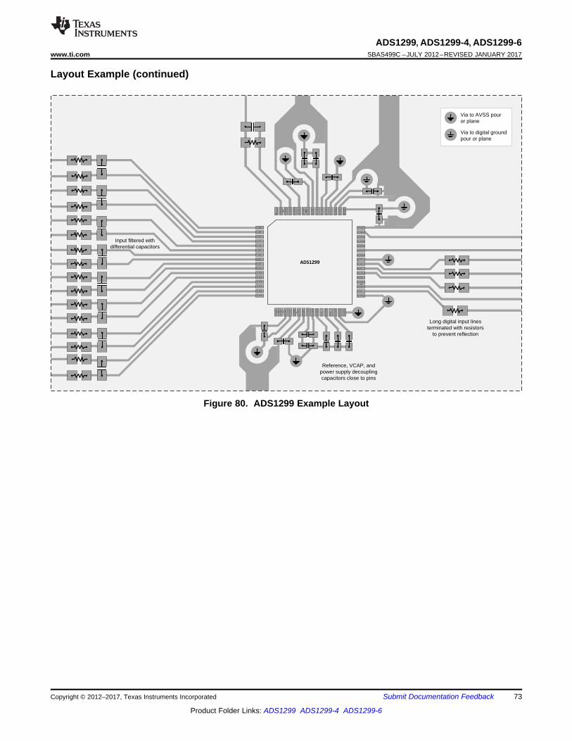
ADS1299
1: IN8N
2: IN8P
3: IN7N
4: IN7P
5: IN6N
6: IN6P
7: IN5N
8: IN5P
9: IN4N
10: IN4P
11: IN3N
12: IN3P
13: IN2N
14: IN2P
15: IN1N
16: IN1P
17: S
RB
1
18: S
RB
2
19: A
VD
D
20: A
VS
S
21: A
VD
D
22: A
VD
D
23: A
VS
S
24: V
RE
FP
25: V
RE
FN
26: V
CA
P4
27: N
C
28: V
CA
P1
29: N
C
30: V
CA
P2
31: R
ES
V1
32: A
VS
S
48: DVDD
47: DRDY
46: GPIO4
45: GPIO3
44: GPIO2
43: DOUT
42: GPIO1
41: DAISY_IN
40: SCLK
39: CS
38: START
37: CLK
36: RESET
35:PWDN
34: DIN
33: DGND
64:
RE
SE
RV
ED
63: B
IAS
OU
T
62: B
IAS
IN
61: B
IAS
INV
60: B
IAS
RE
F
59: A
VD
D
58: A
VS
S
57: A
VS
S
56: A
VD
D
55: V
CA
P3
54: A
VD
D1
53: A
VS
S1
52: C
LKS
EL
51: D
GN
D
50: D
VD
D
49: D
GN
D
Reference, VCAP, and power supply decoupling capacitors close to pins
Input filtered with differential capacitors
Via to AVSS pour or plane
Via to digital ground pour or plane
Long digital input lines terminated with resistors
to prevent reflection
73
ADS1299, ADS1299-4, ADS1299-6www.ti.com SBAS499C –JULY 2012–REVISED JANUARY 2017
Product Folder Links: ADS1299 ADS1299-4 ADS1299-6
Submit Documentation FeedbackCopyright © 2012–2017, Texas Instruments Incorporated
Layout Example (continued)
Figure 80. ADS1299 Example Layout

74
ADS1299, ADS1299-4, ADS1299-6SBAS499C –JULY 2012–REVISED JANUARY 2017 www.ti.com
Product Folder Links: ADS1299 ADS1299-4 ADS1299-6
Submit Documentation Feedback Copyright © 2012–2017, Texas Instruments Incorporated
13 Device and Documentation Support
13.1 Documentation Support
13.1.1 Related DocumentationFor related documentation see the following:• ADS129x Low-Power, 8-Channel, 24-Bit Analog Front-End for Biopotential Measurements• REF50xx Low-Noise, Very Low Drift, Precision Voltage Reference• Improving Common-Mode Rejection Using the Right-Leg Drive Amplifier• ADS1299EEG-FE EEG Front-End Performance Demonstration Kit
13.2 Related LinksThe table below lists quick access links. Categories include technical documents, support and communityresources, tools and software, and quick access to order now.
Table 31. Related Links
PARTS PRODUCT FOLDER ORDER NOW TECHNICALDOCUMENTS
TOOLS &SOFTWARE
SUPPORT &COMMUNITY
ADS1299 Click here Click here Click here Click here Click hereADS1299-4 Click here Click here Click here Click here Click hereADS1299-6 Click here Click here Click here Click here Click here
13.3 Receiving Notification of Documentation UpdatesTo receive notification of documentation updates, navigate to the device product folder on ti.com. In the upperright corner, click on Alert me to register and receive a weekly digest of any product information that haschanged. For change details, review the revision history included in any revised document.
13.4 Community ResourcesThe following links connect to TI community resources. Linked contents are provided "AS IS" by the respectivecontributors. They do not constitute TI specifications and do not necessarily reflect TI's views; see TI's Terms ofUse.
TI E2E™ Online Community TI's Engineer-to-Engineer (E2E) Community. Created to foster collaborationamong engineers. At e2e.ti.com, you can ask questions, share knowledge, explore ideas and helpsolve problems with fellow engineers.
Design Support TI's Design Support Quickly find helpful E2E forums along with design support tools andcontact information for technical support.
13.5 TrademarksE2E is a trademark of Texas Instruments.All other trademarks are the property of their respective owners.
13.6 Electrostatic Discharge CautionThis integrated circuit can be damaged by ESD. Texas Instruments recommends that all integrated circuits be handled withappropriate precautions. Failure to observe proper handling and installation procedures can cause damage.
ESD damage can range from subtle performance degradation to complete device failure. Precision integrated circuits may be moresusceptible to damage because very small parametric changes could cause the device not to meet its published specifications.
13.7 GlossarySLYZ022 — TI Glossary.
This glossary lists and explains terms, acronyms, and definitions.

75
ADS1299, ADS1299-4, ADS1299-6www.ti.com SBAS499C –JULY 2012–REVISED JANUARY 2017
Product Folder Links: ADS1299 ADS1299-4 ADS1299-6
Submit Documentation FeedbackCopyright © 2012–2017, Texas Instruments Incorporated
14 Mechanical, Packaging, and Orderable InformationThe following pages include mechanical, packaging, and orderable information. This information is the mostcurrent data available for the designated devices. This data is subject to change without notice and revision ofthis document. For browser-based versions of this data sheet, refer to the left-hand navigation.

PACKAGE OPTION ADDENDUM
www.ti.com 19-Dec-2016
Addendum-Page 1
PACKAGING INFORMATION
Orderable Device Status(1)
Package Type PackageDrawing
Pins PackageQty
Eco Plan(2)
Lead/Ball Finish(6)
MSL Peak Temp(3)
Op Temp (°C) Device Marking(4/5)
Samples
ADS1299-4PAG ACTIVE TQFP PAG 64 160 Green (RoHS& no Sb/Br)
CU NIPDAU Level-3-260C-168 HR -40 to 85 ADS1299-4
ADS1299-4PAGR ACTIVE TQFP PAG 64 1500 Green (RoHS& no Sb/Br)
CU NIPDAU Level-3-260C-168 HR -40 to 85 ADS1299-4
ADS1299-6PAG ACTIVE TQFP PAG 64 160 Green (RoHS& no Sb/Br)
CU NIPDAU Level-3-260C-168 HR -40 to 85 ADS1299-6
ADS1299-6PAGR ACTIVE TQFP PAG 64 1500 Green (RoHS& no Sb/Br)
CU NIPDAU Level-3-260C-168 HR -40 to 85 ADS1299-6
ADS1299IPAG ACTIVE TQFP PAG 64 160 Green (RoHS& no Sb/Br)
CU NIPDAU Level-3-260C-168 HR -40 to 85 ADS1299
ADS1299IPAGR ACTIVE TQFP PAG 64 1500 Green (RoHS& no Sb/Br)
CU NIPDAU Level-3-260C-168 HR -40 to 85 ADS1299
(1) The marketing status values are defined as follows:ACTIVE: Product device recommended for new designs.LIFEBUY: TI has announced that the device will be discontinued, and a lifetime-buy period is in effect.NRND: Not recommended for new designs. Device is in production to support existing customers, but TI does not recommend using this part in a new design.PREVIEW: Device has been announced but is not in production. Samples may or may not be available.OBSOLETE: TI has discontinued the production of the device.
(2) Eco Plan - The planned eco-friendly classification: Pb-Free (RoHS), Pb-Free (RoHS Exempt), or Green (RoHS & no Sb/Br) - please check http://www.ti.com/productcontent for the latest availabilityinformation and additional product content details.TBD: The Pb-Free/Green conversion plan has not been defined.Pb-Free (RoHS): TI's terms "Lead-Free" or "Pb-Free" mean semiconductor products that are compatible with the current RoHS requirements for all 6 substances, including the requirement thatlead not exceed 0.1% by weight in homogeneous materials. Where designed to be soldered at high temperatures, TI Pb-Free products are suitable for use in specified lead-free processes.Pb-Free (RoHS Exempt): This component has a RoHS exemption for either 1) lead-based flip-chip solder bumps used between the die and package, or 2) lead-based die adhesive used betweenthe die and leadframe. The component is otherwise considered Pb-Free (RoHS compatible) as defined above.Green (RoHS & no Sb/Br): TI defines "Green" to mean Pb-Free (RoHS compatible), and free of Bromine (Br) and Antimony (Sb) based flame retardants (Br or Sb do not exceed 0.1% by weightin homogeneous material)
(3) MSL, Peak Temp. - The Moisture Sensitivity Level rating according to the JEDEC industry standard classifications, and peak solder temperature.
(4) There may be additional marking, which relates to the logo, the lot trace code information, or the environmental category on the device.
(5) Multiple Device Markings will be inside parentheses. Only one Device Marking contained in parentheses and separated by a "~" will appear on a device. If a line is indented then it is a continuationof the previous line and the two combined represent the entire Device Marking for that device.

PACKAGE OPTION ADDENDUM
www.ti.com 19-Dec-2016
Addendum-Page 2
(6) Lead/Ball Finish - Orderable Devices may have multiple material finish options. Finish options are separated by a vertical ruled line. Lead/Ball Finish values may wrap to two lines if the finishvalue exceeds the maximum column width.
Important Information and Disclaimer:The information provided on this page represents TI's knowledge and belief as of the date that it is provided. TI bases its knowledge and belief on informationprovided by third parties, and makes no representation or warranty as to the accuracy of such information. Efforts are underway to better integrate information from third parties. TI has taken andcontinues to take reasonable steps to provide representative and accurate information but may not have conducted destructive testing or chemical analysis on incoming materials and chemicals.TI and TI suppliers consider certain information to be proprietary, and thus CAS numbers and other limited information may not be available for release.
In no event shall TI's liability arising out of such information exceed the total purchase price of the TI part(s) at issue in this document sold by TI to Customer on an annual basis.

TAPE AND REEL INFORMATION
*All dimensions are nominal
Device PackageType
PackageDrawing
Pins SPQ ReelDiameter
(mm)
ReelWidth
W1 (mm)
A0(mm)
B0(mm)
K0(mm)
P1(mm)
W(mm)
Pin1Quadrant
ADS1299-4PAGR TQFP PAG 64 1500 330.0 24.4 13.0 13.0 1.5 16.0 24.0 Q2
ADS1299-6PAGR TQFP PAG 64 1500 330.0 24.4 13.0 13.0 1.5 16.0 24.0 Q2
ADS1299IPAGR TQFP PAG 64 1500 330.0 24.4 13.0 13.0 1.5 16.0 24.0 Q2
PACKAGE MATERIALS INFORMATION
www.ti.com 20-Dec-2016
Pack Materials-Page 1

*All dimensions are nominal
Device Package Type Package Drawing Pins SPQ Length (mm) Width (mm) Height (mm)
ADS1299-4PAGR TQFP PAG 64 1500 367.0 367.0 45.0
ADS1299-6PAGR TQFP PAG 64 1500 367.0 367.0 45.0
ADS1299IPAGR TQFP PAG 64 1500 367.0 367.0 45.0
PACKAGE MATERIALS INFORMATION
www.ti.com 20-Dec-2016
Pack Materials-Page 2
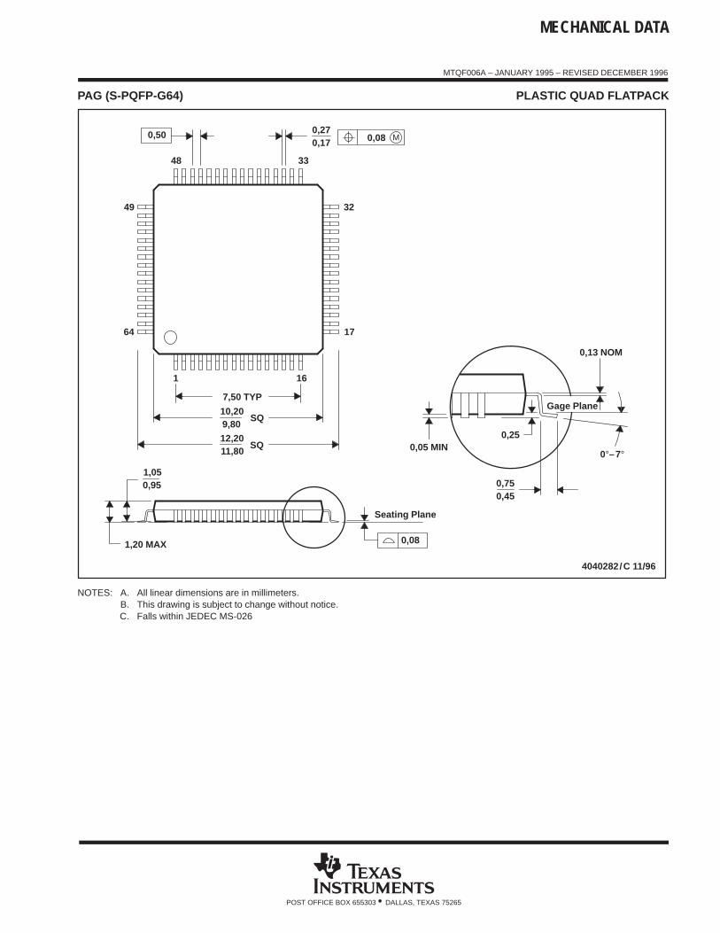
MECHANICAL DATA
MTQF006A – JANUARY 1995 – REVISED DECEMBER 1996
POST OFFICE BOX 655303 • DALLAS, TEXAS 75265
PAG (S-PQFP-G64) PLASTIC QUAD FLATPACK
0,13 NOM
0,25
0,450,75
Seating Plane
0,05 MIN
4040282/C 11/96
Gage Plane
33
0,170,27
16
48
1
7,50 TYP
49
64
SQ
9,80
1,050,95
11,8012,20
1,20 MAX
10,20SQ
17
32
0,08
0,50 M0,08
0°–7°
NOTES: A. All linear dimensions are in millimeters.B. This drawing is subject to change without notice.C. Falls within JEDEC MS-026

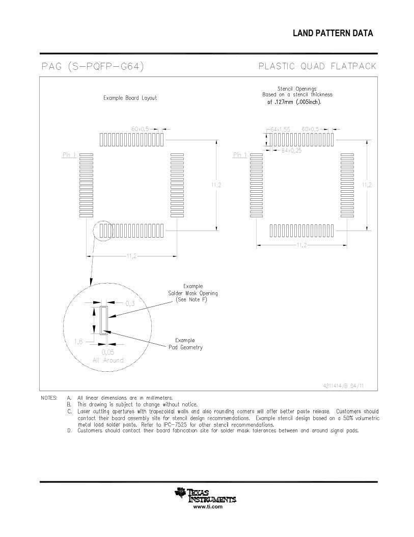

IMPORTANT NOTICE
Texas Instruments Incorporated (TI) reserves the right to make corrections, enhancements, improvements and other changes to itssemiconductor products and services per JESD46, latest issue, and to discontinue any product or service per JESD48, latest issue. Buyersshould obtain the latest relevant information before placing orders and should verify that such information is current and complete.TI’s published terms of sale for semiconductor products (http://www.ti.com/sc/docs/stdterms.htm) apply to the sale of packaged integratedcircuit products that TI has qualified and released to market. Additional terms may apply to the use or sale of other types of TI products andservices.Reproduction of significant portions of TI information in TI data sheets is permissible only if reproduction is without alteration and isaccompanied by all associated warranties, conditions, limitations, and notices. TI is not responsible or liable for such reproduceddocumentation. Information of third parties may be subject to additional restrictions. Resale of TI products or services with statementsdifferent from or beyond the parameters stated by TI for that product or service voids all express and any implied warranties for theassociated TI product or service and is an unfair and deceptive business practice. TI is not responsible or liable for any such statements.Buyers and others who are developing systems that incorporate TI products (collectively, “Designers”) understand and agree that Designersremain responsible for using their independent analysis, evaluation and judgment in designing their applications and that Designers havefull and exclusive responsibility to assure the safety of Designers' applications and compliance of their applications (and of all TI productsused in or for Designers’ applications) with all applicable regulations, laws and other applicable requirements. Designer represents that, withrespect to their applications, Designer has all the necessary expertise to create and implement safeguards that (1) anticipate dangerousconsequences of failures, (2) monitor failures and their consequences, and (3) lessen the likelihood of failures that might cause harm andtake appropriate actions. Designer agrees that prior to using or distributing any applications that include TI products, Designer willthoroughly test such applications and the functionality of such TI products as used in such applications.TI’s provision of technical, application or other design advice, quality characterization, reliability data or other services or information,including, but not limited to, reference designs and materials relating to evaluation modules, (collectively, “TI Resources”) are intended toassist designers who are developing applications that incorporate TI products; by downloading, accessing or using TI Resources in anyway, Designer (individually or, if Designer is acting on behalf of a company, Designer’s company) agrees to use any particular TI Resourcesolely for this purpose and subject to the terms of this Notice.TI’s provision of TI Resources does not expand or otherwise alter TI’s applicable published warranties or warranty disclaimers for TIproducts, and no additional obligations or liabilities arise from TI providing such TI Resources. TI reserves the right to make corrections,enhancements, improvements and other changes to its TI Resources. TI has not conducted any testing other than that specificallydescribed in the published documentation for a particular TI Resource.Designer is authorized to use, copy and modify any individual TI Resource only in connection with the development of applications thatinclude the TI product(s) identified in such TI Resource. NO OTHER LICENSE, EXPRESS OR IMPLIED, BY ESTOPPEL OR OTHERWISETO ANY OTHER TI INTELLECTUAL PROPERTY RIGHT, AND NO LICENSE TO ANY TECHNOLOGY OR INTELLECTUAL PROPERTYRIGHT OF TI OR ANY THIRD PARTY IS GRANTED HEREIN, including but not limited to any patent right, copyright, mask work right, orother intellectual property right relating to any combination, machine, or process in which TI products or services are used. Informationregarding or referencing third-party products or services does not constitute a license to use such products or services, or a warranty orendorsement thereof. Use of TI Resources may require a license from a third party under the patents or other intellectual property of thethird party, or a license from TI under the patents or other intellectual property of TI.TI RESOURCES ARE PROVIDED “AS IS” AND WITH ALL FAULTS. TI DISCLAIMS ALL OTHER WARRANTIES ORREPRESENTATIONS, EXPRESS OR IMPLIED, REGARDING RESOURCES OR USE THEREOF, INCLUDING BUT NOT LIMITED TOACCURACY OR COMPLETENESS, TITLE, ANY EPIDEMIC FAILURE WARRANTY AND ANY IMPLIED WARRANTIES OFMERCHANTABILITY, FITNESS FOR A PARTICULAR PURPOSE, AND NON-INFRINGEMENT OF ANY THIRD PARTY INTELLECTUALPROPERTY RIGHTS. TI SHALL NOT BE LIABLE FOR AND SHALL NOT DEFEND OR INDEMNIFY DESIGNER AGAINST ANY CLAIM,INCLUDING BUT NOT LIMITED TO ANY INFRINGEMENT CLAIM THAT RELATES TO OR IS BASED ON ANY COMBINATION OFPRODUCTS EVEN IF DESCRIBED IN TI RESOURCES OR OTHERWISE. IN NO EVENT SHALL TI BE LIABLE FOR ANY ACTUAL,DIRECT, SPECIAL, COLLATERAL, INDIRECT, PUNITIVE, INCIDENTAL, CONSEQUENTIAL OR EXEMPLARY DAMAGES INCONNECTION WITH OR ARISING OUT OF TI RESOURCES OR USE THEREOF, AND REGARDLESS OF WHETHER TI HAS BEENADVISED OF THE POSSIBILITY OF SUCH DAMAGES.Unless TI has explicitly designated an individual product as meeting the requirements of a particular industry standard (e.g., ISO/TS 16949and ISO 26262), TI is not responsible for any failure to meet such industry standard requirements.Where TI specifically promotes products as facilitating functional safety or as compliant with industry functional safety standards, suchproducts are intended to help enable customers to design and create their own applications that meet applicable functional safety standardsand requirements. Using products in an application does not by itself establish any safety features in the application. Designers mustensure compliance with safety-related requirements and standards applicable to their applications. Designer may not use any TI products inlife-critical medical equipment unless authorized officers of the parties have executed a special contract specifically governing such use.Life-critical medical equipment is medical equipment where failure of such equipment would cause serious bodily injury or death (e.g., lifesupport, pacemakers, defibrillators, heart pumps, neurostimulators, and implantables). Such equipment includes, without limitation, allmedical devices identified by the U.S. Food and Drug Administration as Class III devices and equivalent classifications outside the U.S.TI may expressly designate certain products as completing a particular qualification (e.g., Q100, Military Grade, or Enhanced Product).Designers agree that it has the necessary expertise to select the product with the appropriate qualification designation for their applicationsand that proper product selection is at Designers’ own risk. Designers are solely responsible for compliance with all legal and regulatoryrequirements in connection with such selection.Designer will fully indemnify TI and its representatives against any damages, costs, losses, and/or liabilities arising out of Designer’s non-compliance with the terms and provisions of this Notice.
Mailing Address: Texas Instruments, Post Office Box 655303, Dallas, Texas 75265Copyright © 2018, Texas Instruments Incorporated