ADP1043A Evaluation Software Reference Guide Preliminary ... · ADP1043A Evaluation Software...
35
ADP1043A Evaluation Software Reference Guide Preliminary Technical Data EVAL-ADP1043A-GUI-RG Rev. A Information furnished by Analog Devices is believed to be accurate and reliable. However, no responsibility is assumed by Analog Devices for its use, nor for any infringements of patents or other rights of third parties that may result from its use. Specifications subject to change without notice. No license is granted by implication or otherwise under any patent or patent rights of Analog Devices. Trademarks and registered trademarks are the property of their respective owners. One Technology Way, P.O. Box 9106, Norwood, MA 02062-9106, U.S.A. Tel: 781.329.4700 www.analog.com Fax: 781.461.3113 ©2007 Analog Devices, Inc. All rights reserved. GENERAL DESCRIPTION This user guide gives describes the various controls and indicators of the ADP1043A Evaluation Software. It gives the details of what each button on the GUI does, in terms of the register that is being updated, along with a brief description. Figure 1. GUI Main Interface Window
Transcript of ADP1043A Evaluation Software Reference Guide Preliminary ... · ADP1043A Evaluation Software...

ADP1043A Evaluation SoftwareReference Guide
Preliminary Technical Data EVAL-ADP1043A-GUI-RG
Rev. A Information furnished by Analog Devices is believed to be accurate and reliable. However, no responsibility is assumed by Analog Devices for its use, nor for any infringements of patents or other rights of third parties that may result from its use. Specifications subject to change without notice. No license is granted by implication or otherwise under any patent or patent rights of Analog Devices. Trademarks and registered trademarks are the property of their respective owners.
One Technology Way, P.O. Box 9106, Norwood, MA 02062-9106, U.S.A.Tel: 781.329.4700 www.analog.com Fax: 781.461.3113 ©2007 Analog Devices, Inc. All rights reserved.
GENERAL DESCRIPTION This user guide gives describes the various controls and indicators of the ADP1043A Evaluation Software. It gives the details of what each button on the GUI does, in terms of the register that is being updated, along with a brief description.
Figure 1. GUI Main Interface Window

EVAL-ADP1043A-GUI-RG Preliminary Technical Data
Rev. A | Page 2 of 35
TABLE OF CONTENTS General Description ......................................................................... 1
Revision History ............................................................................... 2
GUI Controls ..................................................................................... 3
Link................................................................................................. 3
Structural navigation .................................................................... 3
Windows navigation .................................................................... 4
Tools ............................................................................................... 4
Dashboard ..................................................................................... 5
Setup ................................................................................................... 6
Voltage Settings ................................................................................. 7
OrFET Settings .................................................................................. 9
CS1 Settings ..................................................................................... 11
CS2 Settings ..................................................................................... 13
Register Access ................................................................................ 15
Topology PWM and SR Setup ...................................................... 16
General......................................................................................... 16
Modulating Edges....................................................................... 18
Adaptive dead time .................................................................... 19
Resonant Mode ........................................................................... 20
Filter Settings .................................................................................. 22
Share Bus Settings ........................................................................... 24
General settings .............................................................................. 25
Flag Settings .................................................................................... 27
Monitor ............................................................................................ 30
Flags and Power Monitoring ......................................................... 32
REVISION HISTORY 06/09—Rev. 1
09/09—Rev. 2

Preliminary Technical Data EVAL-ADP1043A-GUI-RG
Rev. A | Page 3 of 35
GUI CONTROLS LINK
Figure 2.
Table 1. Referring to Figure 2 No. Name REG Bits R/W Description “USB to I2C interface”
Number This number shows the last three digits of the ‘‘USB to I2C interface’’ connected
to ADP1043A. This number is also physically printed on the ‘‘USB to I2C Interface’’
ADP1043A Address This number shows the address of ADP1043A the GUI is connected to.
Communication link This animated indicator shows if the GUI is communicating with ADP1043A
Scan The GUI scans for all the ADP1043A connected to the computer. This helps in connecting and disconnecting devices once the GUI is already running.
Save/Load Options This control opens the Tools window
Dashboard This control opens the Dashboard window
Update EEPROM 0x5E 0x7B
[7:0] W This control writes the contents of the registers to the EEPROM of ADP1043AThis is done by writing 0h twitce to register 0x5E, followed by writing 0h to 0x7B, wait for 40ms and followed by writing 1h to 0x5E
Spy This control opens the Spy window
STRUCTURAL NAVIGATION
Figure 3.
Table 2. Referring to Figure 3 No. Name REG Bits R/W Description Device – Window Info This indicator shows the device address and the window name of the window
which is currently open
Structural Navigation If you have only one device connected to the GUI, then clicking on the buttons opens the respective windows. If you have multiple devices connected, then clicking on the buttons opens the window for the device selected in the ‘‘Link’’ section shown above in Figure 2
1 2 3
4 5
1
2
5
3
4
1 2
1
2
6 7 8
7
6
8

EVAL-ADP1043A-GUI-RG Preliminary Technical Data
Rev. A | Page 4 of 35
WINDOWS NAVIGATION
Figure 4.
Table 3. Referring to Figure 4 No. Name REG Bits R/W Description Arrows The arrows move the tabs in the respective directions
Tabs The tabs open the window whose name and device address is displayed on it
TOOLS
Figure 5.
Table 4. Referring to Figure 5 No. Name REG Bits R/W Description Save Register Settings This control saves the contents of the register map of the device selected in the
‘‘Link’’ section shown above in Figure 2, to a “.43r” file
Load register Settings This control loads the contents of the register map to the device selected in the ‘‘Link’’ section shown above in Figure 2, from a “.43r” file
Save Board Settings This control saves the information about the extrenal components required by the GUI to a “.43b” file
Load Board Settings This control loads the information about the extrenal components required by the GUI from a “.43b” file
Update GUI This control connects to” www.analog.com” and redirects you to the page which has the latest version of the GUI
Reference Guide This control opens the GUI Reference Guide
1
2
1
2
1 2 3 4 5
1
2
5
3
4
6
6
Preliminary Technical Data EVAL-ADP1043A-GUI-RG
Rev. A | Page 5 of 35
DASHBOARD
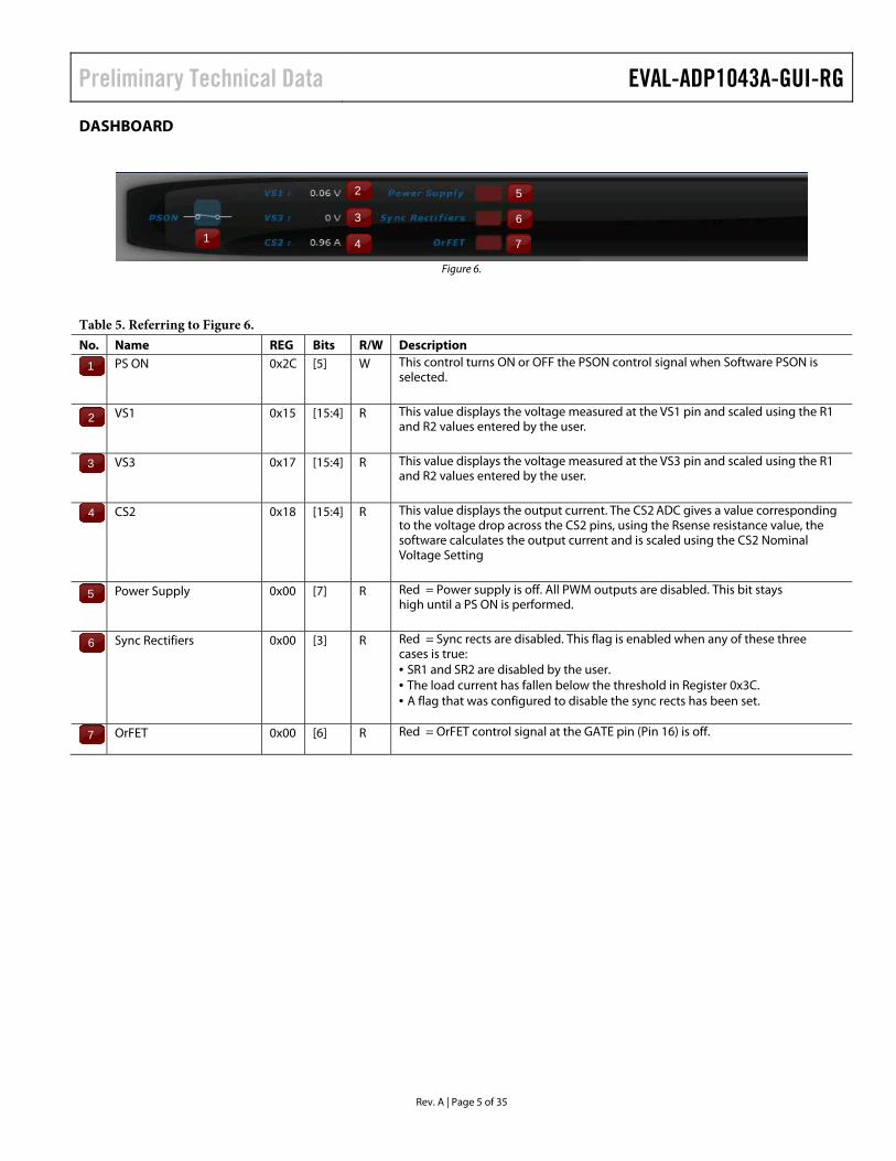
Figure 6.
Table 5. Referring to Figure 6. No. Name REG Bits R/W Description PS ON 0x2C [5] W This control turns ON or OFF the PSON control signal when Software PSON is
selected.
VS1 0x15 [15:4] R This value displays the voltage measured at the VS1 pin and scaled using the R1 and R2 values entered by the user.
VS3 0x17 [15:4] R This value displays the voltage measured at the VS3 pin and scaled using the R1 and R2 values entered by the user.
CS2 0x18 [15:4] R This value displays the output current. The CS2 ADC gives a value corresponding to the voltage drop across the CS2 pins, using the Rsense resistance value, the software calculates the output current and is scaled using the CS2 Nominal Voltage Setting
Power Supply 0x00 [7] R Red = Power supply is off. All PWM outputs are disabled. This bit stayshigh until a PS ON is performed.
Sync Rectifiers 0x00 [3] R Red = Sync rects are disabled. This flag is enabled when any of these threecases is true: • SR1 and SR2 are disabled by the user. • The load current has fallen below the threshold in Register 0x3C. • A flag that was configured to disable the sync rects has been set.
OrFET 0x00 [6] R Red = OrFET control signal at the GATE pin (Pin 16) is off.
1
2
3
4
5
1
6
7
2
3
5
4
6
7

EVAL-ADP1043A-GUI-RG Preliminary Technical Data
Rev. A | Page 6 of 35
SETUP
Figure 7.
Table 6. Referring to Figure 7 No. Name REG Bits R/W Description External Components These external components values are entered by the user, which helps the GUI
in calculating scale factors, full loop phase and gain response of the system. The user can also select various other options like topology for display purposes
High-Side Current Sensing
0x24 [7] W The user can select between High-Side or Low-Side Current Sensing by clicking on this control
ADP1043A Setup Blocks The grey block represents ADP1043A and the blue blocks represent the various setup blocks of the ADP1043A. These blue blocks can be clicked to open the corresponding window for settings
Resonant Mode 0x40 [7:0] W The user can select between Resonant Mode or other topologies by clicking on this control
1
2
3
1
2
3
4
4

Preliminary Technical Data EVAL-ADP1043A-GUI-RG
Rev. A | Page 7 of 35
VOLTAGE SETTINGS
Figure 8.
Table 7. Referring to Figure 8. No. Name REG Bits R/W Description VS1 Trim Value 0x38 [7:0] W This sets the amount of gain trim that is applied to the VS1 ADC reading. This
control trims the voltage at the VS1 pin for external resistor tolerances. This control is trimmed until the VS1 Value indicator displays the desired nominal voltage
VS1 Value 0x15 [15:4] R This value displays the voltage measured at the VS1 pin and scaled using the resistor values entered by the user in the Setup Window.
VS2 Trim Value 0x39 [7:0] W This sets the amount of gain trim that is applied to the VS2 ADC reading. This control trims the voltage at the VS2 pin for external resistor tolerances. This control is trimmed until the VS2 Value indicator displays the desired nominal voltage
VS2 Value 0x16 [15:4] R This value displays the voltage measured at the VS2 pin and scaled using the resistor values entered by the user in the Setup Window.
VS3 Trim Value 0x3A [7:0] W This sets the amount of gain trim that is applied to the VS3 ADC reading. This control trims the voltage at the VS3 pin for external resistor tolerances. This control is trimmed until the VS3 Value indicator displays the desired nominal voltage. The Output Voltage Setting Should be set to 100% while trimming VS3
Output Voltage Setting 0x31 [7:0] W This control is used to change the output voltage. It is programmable from 0% to 155% of nominal voltage.
1 2
3 4
5
6
7
8
9
10
11
12 13
14
15
16
17
1
2
2
3
4
4
6
7
6
5
18

EVAL-ADP1043A-GUI-RG Preliminary Technical Data
Rev. A | Page 8 of 35
Table 8. Referring to Figure 8. No. Name REG Bits R/W Description VS3 Value 0x17 [15:4] R This value displays the voltage measured at the VS3 pin and scaled using the
resistor values entered by the user in the Setup Window.
Auto Trim VS1, VS2 and VS3
Follow the three steps mentioned in the ‘‘Voltage Trim Procedure’’, to trim VS3. Then click on this button to Auto-Trim VS1 and VS2
VS1 OVP Setting 0x32 [7:3] W Local overvoltage limit. This range is programmable from 107.7% to 145.3% of the nominal VS1 voltage. 0x00 corresponds to 108.5%. Each LSB results in an increase of 1.21%.
VS1 OV Debounce 0x32 [1:0] W Delay before setting the OVP Flag
VS1 UVP Setting 0x34 [6:0] W This control sets the UVP limit. The range is programmable from 0% to 155% of the nominal VS1 voltage. Each LSB increases the voltage by 155% / 128 = 1.21%
VS3 OVP Setting 0x33 [7:3] W Local overvoltage limit. This range is programmable from 107.7% to 145.3% of the nominal VS3 voltage. 0x00 corresponds to 107.7%. Each LSB results in an increase of 1.21%.
VS3 OV Debounce 0x33 [1:0] W Delay before setting the OVP Flag
Load OVP (VS2 or VS3) Action
0x09 [1:0] W This control sets the action that the ADP1043A needs to take once the flag is set.
Timing [3] W This control sets a debounce between the flag being set and the action that the ADP1043A needs to take.
Resolve Issue [2] W This control selects whether to re-enable ADP1043A or remain disabled after the flag is set.
Line Impedance Action
0x0C [1:0] W This control sets the action that the ADP1043A needs to take once the flag is set.
Timing [3] W This control sets a debounce between the flag being set and the action that the ADP1043A needs to take.
Resolve Issue [2] W This control selects whether to re-enable ADP1043A or remain disabled after the flag is set.
Local OVP (VS1) Action
0x0A [5:4] W This control sets the action that the ADP1043A needs to take once the flag is set.
Timing [7] W This control sets a debounce between the flag being set and the action that the ADP1043A needs to take.
Resolve Issue [6] W This control selects whether to re-enable ADP1043A or remain disabled after the flag is set.
Local UVP (VS1) Action
0x0B [1:0] W This control sets the action that the ADP1043A needs to take once the flag is set.
Timing [3] W This control sets a debounce between the flag being set and the action that the ADP1043A needs to take.
Resolve Issue [2] W This control selects whether to re-enable ADP1043A or remain disabled after the flag is set.
Regulate with VS3 at all times
0x33 [2] W Set the regulating point to VS3 at all times. (If not set, then the ADP1043A uses the VS1 voltage as the regulating point during soft-start)
7
9
8
10
11
12
13
16
17
15
14
18

Preliminary Technical Data EVAL-ADP1043A-GUI-RG
Rev. A | Page 9 of 35
ORFET SETTINGS
Figure 9.
Table 9. Referring to Figure 9. No. Name REG Bits R/W Description OrFET Enable Threshold 0x30 [5:4] W This control programs the voltage difference between VS1 and VS2 before the
OrFET is enabled.
Fast OrFET Threshold 0x30 [3:2] W This control programs the threshold voltage difference between CS2+ and CS2− at which the OrFET is disabled.
Debounce 0x30 [1] W This control determines the debounce on the fast OrFET control before it disables the OrFET.
Fast OrFET Enabled 0x30 [0] W This switch enables or disable Fast OrFET
Accurate OrFET Threshold
0x30 [7:6] W This control programs the voltage difference between CS2+ and CS2− at which the Reverse Voltage flag is set.
Reverse Voltage (Accurate OrFET Threshold) Action
0x0C [5:4] W This control sets the action that the ADP1043A needs to take once the flag is set.
Timing [7] W This control sets a debounce between the flag being set and the action that the ADP1043A needs to take.
Resolve Issue [6] W This control selects whether to re-enable ADP1043A or remain disabled after the flag is set.
1
2
3
4
5
1
2
3
4 5
6
7
6

EVAL-ADP1043A-GUI-RG Preliminary Technical Data
Rev. A | Page 10 of 35
Table 10. Referring to Figure 9 No. Name REG Bits R/W Description Gate Polarity 0x2D [1] W This switch sets the polarity of the OrFET Gate control pin
7
Preliminary Technical Data EVAL-ADP1043A-GUI-RG
Rev. A | Page 11 of 35
CS1 SETTINGS
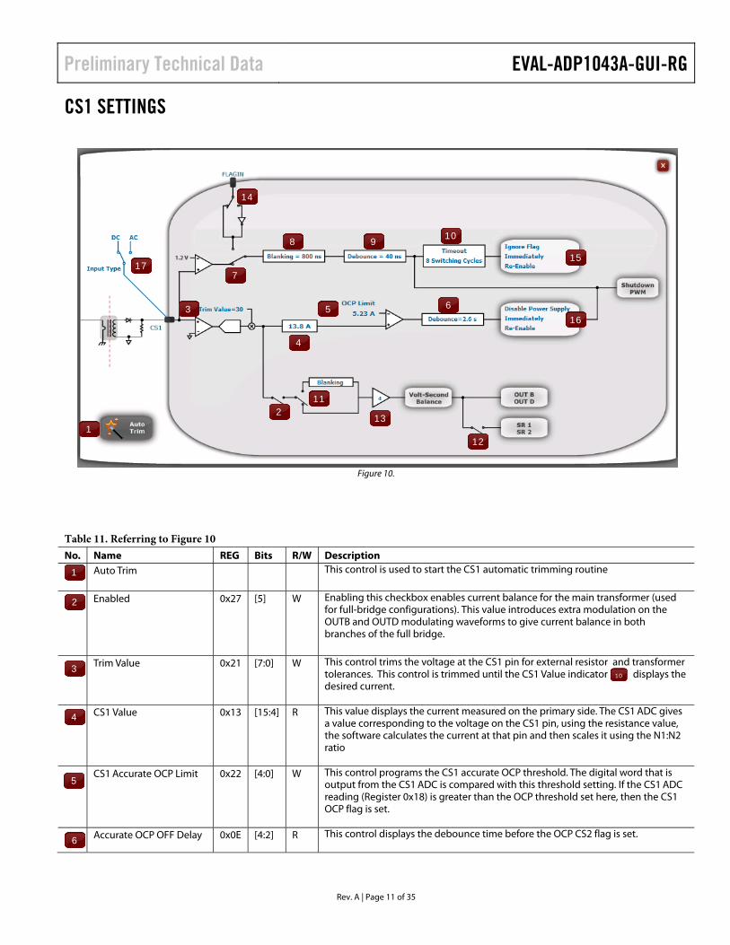
Figure 10.
Table 11. Referring to Figure 10 No. Name REG Bits R/W Description Auto Trim This control is used to start the CS1 automatic trimming routine
Enabled 0x27 [5] W Enabling this checkbox enables current balance for the main transformer (used
for full-bridge configurations). This value introduces extra modulation on the OUTB and OUTD modulating waveforms to give current balance in both branches of the full bridge.
Trim Value 0x21 [7:0] W This control trims the voltage at the CS1 pin for external resistor and transformer tolerances. This control is trimmed until the CS1 Value indicator displays the desired current.
CS1 Value 0x13 [15:4] R This value displays the current measured on the primary side. The CS1 ADC gives a value corresponding to the voltage on the CS1 pin, using the resistance value, the software calculates the current at that pin and then scales it using the N1:N2 ratio
CS1 Accurate OCP Limit 0x22 [4:0] W This control programs the CS1 accurate OCP threshold. The digital word that is output from the CS1 ADC is compared with this threshold setting. If the CS1 ADC reading (Register 0x18) is greater than the OCP threshold set here, then the CS1 OCP flag is set.
Accurate OCP OFF Delay 0x0E [4:2] R This control displays the debounce time before the OCP CS2 flag is set.
1
2
3
4
5 6
7
8 9 10
11
12
13
14
15
16
1
2
3 10
4
6
5
17

EVAL-ADP1043A-GUI-RG Preliminary Technical Data
Rev. A | Page 12 of 35
Table 12. Referring to Figure 10 No. Name REG Bits R/W Description Fast OCP Bypass 0x27 [4] W Disabling this switch means that the FLAGIN pin is used for CS1 OCP instead of
the CS1 pin. Enabling it means that the Fast OCP comparator is used.
Blanking 0x22 [7:5] W This control determines the blanking time for CS1 before fast OCP is enabled. This time is measured from the start of a switching cycle. It is synchronized with the rising edge of OUTB and OUTD. If regulating using OUTAUX, it is synchronized with the rising edge of OUTAUX.
Debounce 0x27 [7:6] R This control displays the CS1 debounce value. This is the minimum timethat the CS1 signal must be constantly above the fast OCP limit before it shuts down the PWMs. Once this happens, all PWM’s are disabled for the remainder of the switching cycle.
Timeout 0x27 [1:0] W If the CS1 Fast OCP comparator is set, all PWM’s are immediately disabled for the remainder of the switching cycle. The PWM’s resume as normal at the beginning of the next switching cycle. This sets the number of consecutive switching cycles where the comparator is set before the CS1 FAST OCP flag is set.
Leading Edge Blanking 0x27 [2] R/W Setting this switch to ‘‘Blanking’’ means that the current spike at the beginning of each CS1 reading is ignored by the VS Balance circuit
VS Balance on SR PWMs 0x52 [1] R/W Enabling this switch means that the VSBalance circuit will also modulate SR1 and SR2, along with OUTB and OUTD. When set, it is the rising edge of SR1 and SR2 that the VSBalance modulation is applied to.
Gain 0x28 [1:0] R/W If the CS1 Fast OCP comparator is set, all PWM’s are immediately disabled for the remainder of the switching cycle. The PWM’s resume as normal at the beginning of the next switching cycle. This sets the number of consecutive switching cycles where the comparator is set before the CS1 FAST OCP flag is set.
Flag-In Polarity 0x2D [2] W This switch sets the polarity of the FlagIN input pin
CS1 Fast OCP Action
0x08
[5:4] W This control sets the action that the ADP1043A performs once this flag is set.
Timing 0x08 0x27
[7] [7:6]
W This sets the debounce between the flag being set and the action.
Resolve Issue [6] W This sets whether to re-enable or remain disabled after the flag is set.
CS1 Accurate OCP Action
0x08 [1:0] W This control sets the action that the ADP1043A needs to take once the flag is set.
Timing 0x08 0x0E
[3] [4:2]
W This control sets a debounce between the flag being set and the action that the ADP1043A needs to take.
Resolve Issue [2] W This control selects whether to re-enable ADP1043A or remain disabled after the flag is set.
CS1 Input Type This switch lets you specify the type of signal the CS1 pin is seeing. This value is used then used to accurately calculate CS1 value
7
9
8
10
12
13
11
14
15
16
17

Preliminary Technical Data EVAL-ADP1043A-GUI-RG
Rev. A | Page 13 of 35
CS2 SETTINGS
Figure 11.
Table 13. Referring to Figure 11. No. Name REG Bits R/W Description Auto Trim This control is used to start the CS1 automatic trimming routine
CS2 Nominal Voltage 0x23 [7:6] W This control sets the nominal full-load voltage drop across the sense resistor
Offset Trim 0x24 [6:0] W This control calibrates the secondary side (CS2) current sense common-mode
error. It calibrates for errors in the resistor divider network.
Digital Offset Trim 0x25 [7:0] W This control is used to calibrate the CS2 value that is read in Register 0x18
Gain Trim 0x23 [5:0] W This control calibrates the secondary side (CS2) current sense gain. It calibrates for errors in the sense resistor.
CS2 Value 0x18 [15:4] R This value displays the output current. The CS2 ADC gives a value corresponding to the voltage drop across the CS2 pins, using the Rsense resistance value, the software calculates the output current and is scaled using the CS2 Nominal Voltage Setting
CS2 Accurate OCP Limit 0x26 [7:0] W This control programs the CS2 OCP threshold. The digital word that is output from the CS2 ADC is compared with this threshold setting. If the CS2 ADC reading (Register 0x18) is greater than the OCP threshold set here, then the CS2 OCP flag is set. This value should be programmed only after the CS2 offset, gain, and digital trims have been performed.
Table 14. Referring to Figure 11. No. Name REG Bits R/W Description
1
2
3
4
5
6
7 8
9
10
11
12
13
14
1
2
3
4
5
6
7
8

EVAL-ADP1043A-GUI-RG Preliminary Technical Data
Rev. A | Page 14 of 35
Accurate OCP OFF Delay 0x0E [4:2] R This control displays the debounce before the OCP CS2 flag is set.
CS2 Accurate OCP Action
0x09 [5:4] W This control sets the action that the ADP1043A needs to take once the flag is set.
Timing 0x09 0x0E
[7] [4:2]
W This control sets a debounce between the flag being set and the action that the ADP1043A needs to take.
Resolve Issue [6] W This control selects whether to re-enable ADP1043A or remain disabled after the flag is set.
Load Line Setting 0x36 [2:0] W This control sets the impedance for the Load Line Setting
Load Line Enable 0x36 [3] W This switch enables or disables the load line. This sets how much the output voltage decreases from nominal at full load. For example, a 12V system, programmed with an 8% load-line means that the output voltage will vary from 12V at no load to 11.04V at 100% load.
Light Load Current Threshold
0x3B [2:0] W This control sets the load current limit on the CS2 ADC below which the Sync Rectifier (SR1 and SR2) outputs are disabled. This value also determines the point at which the power supply goes into DCM mode. Below this limit, the DCM filter registers are used. Above this limit, the CCM filter registers are used. This value is programmable from 0 to 46mV of the CS2 ADC . There is an 8mV hysteresis on this signal.
Constant Current Mode 0x27 [3] W This switch is used to enable constant current mode
Disable OUT”X” 0x3B [7:3] W Enabling this checkbox means that the corresponding output will also be disabled if the load current drops below the Light Load Current threshold.
11
9
10
12
13
14

Preliminary Technical Data EVAL-ADP1043A-GUI-RG
Rev. A | Page 15 of 35
REGISTER ACCESS
Figure 12.
Table 15. Referring to Figure 12. No. Name REG Bits R/W Description Register Map 0x00
– 0x7E
This control displays the complete ADP1043A register map, Selecting any particular register will display the data contained in that register, and will allow this register to be read and written to.
Register Details These set of indicators display the selected register’s (selected in )Command Name, Code and its value in hexadecimal and decimal formats.
Bit Display This control / indicator displays the current value of the selected register, and can be modified by clicking on the individual bits.
Read This control reads the value of the register selected by control
Write This control writes the value to the register selected by control
Continuous Read If this checkbox is enabled then the GUI will continuously read the value of the register selected in control
Disable Automatic Read-Back
The GUI automatically does a read operation after a write operation to verify if the write operation was successful. Enabling this checkbox disables this automatic read-back feature.
Description This indicator displays the description of the selected register
1
2
3
4 5
6
7
1
2
3
1
5
7
6
4 1
1
1
8
8

EVAL-ADP1043A-GUI-RG Preliminary Technical Data
Rev. A | Page 16 of 35
TOPOLOGY PWM AND SR SETUP GENERAL
Figure 13.
Table 16. Referring to Figure 13. No. Name REG Bits R/W Description Disable “XXXXX” 0x5D [7:1] Enabling this checkbox disables the corresponding output
T”X” < > This Control increases or decreases the corresponding edge timing in 5ns steps
PWM Edges 0x41
0x43 0x45 0x47 0x49 0x4B 0x4D 0x4F 0x51 0x53 0x55 0x57 0x59 0x5B
[7:0] W Both the rising and falling PWM edges can be clicked on and dragged to move to the desired position to set the positive and negative edge timings
1
2 3
4
5
6
7
8
9
10
11
12
13
14 15
16 17
1
2
3

Preliminary Technical Data EVAL-ADP1043A-GUI-RG
Rev. A | Page 17 of 35
Table 17. Referring to Figure 13. No. Name REG Bits R/W Description Modulation Limits Box These boxes display the modulation limits for that edge. These are set using
controls . Changing the limits will be displayed here.
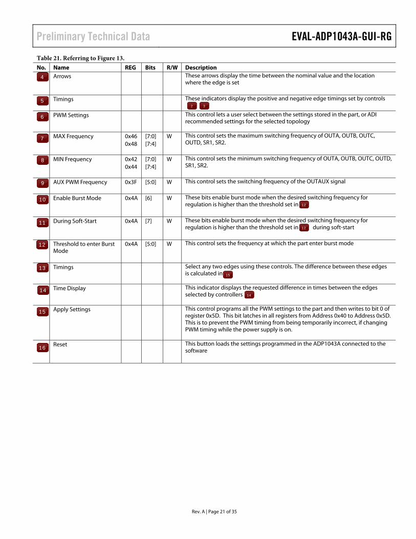
Timings These indicators display the positive and negative edge timings set by controls
PWM Settings This control lets a user select between the settings stored in the part, or ADI recommended settings for the selected topology
PWM Frequency 0x40 [5:0] W This control sets the switching frequency of OUTA, OUTB, OUTC, OUTD, SR1, SR2.
AUX PWM Frequency 0x3F [5:0] W This control sets the switching frequency of the OUTAUX signal
PWM Full-Bridge Mode Enabled
0x2E [7] W Enable this control when operating in full-bridge mode. This mode distributes the modulation equally between two PWMs instead of one. It affects the modulation high limit and the modulation low limit settings.
Modulation High Limit 0x2E [6:4] W This control sets the maximum allowed modulation that will be applied to a PWM. The value is a percentage of the switching period. Changes here will be displayed in
Modulation Low Limit 0x2E [1:0] W This control sets the minimum allowed modulation that will be applied to a PWM. If the modulation calculated is to be lower than this limit, pulse skipping can be enabled. The value is a percentage of the switching period. Changes here will be displayed in
Pulse Skipping Enabled 0x2E [2] W Enabling this checkbox enables pulse skipping mode. If the ADP1043A requires a duty cycle lower than the Modulation Low Limit, pulse skipping will be enabled.
Regulate with OUTAUX 0x5C [1] W If this checkbox is enabled then control loop PWM modulation is regulated by OUTAUX. The CS1 blanking signal is synchronized with OUTAUX If this checkbox is disabled then control loop PWM modulation is regulated by OUTA, OUTB, OUTC, OUTD, SR1 and SR2.
Timings Select any two edges using these controls. The difference between these edges is calculated in
Time Display This indicator displays the requested difference in times between the edges selected by controllers
Apply Settings This control programs all the PWM settings to the part and then writes to bit 0 of register 0x5D. This bit latches in all registers from Address 0x40 to Address 0x5D. This is to prevent the PWM timing from being temporarily incorrect, if changing PWM timing while the power supply is on.
Reset This button loads the settings programmed in the ADP1043A connected to the software
4
6
7
5
8
9
10
11
9 10
12
13
11
2 3
12
14
14
15
17
16
4
4
15

EVAL-ADP1043A-GUI-RG Preliminary Technical Data
Rev. A | Page 18 of 35
MODULATING EDGES
Figure 14.
Table 18. Referring to Figure 14. No. Name REG Bits R/W Description Modulation on T “X” Edge 0x42
0x44 0x46 0x48 0x4A 0x4C 0x4E 0x50 0x52 0x54 0x56 0x58 0x5A 0x5C
[3] W Enabling this checkbox enables modulation on the corresponding edge
1
1

Preliminary Technical Data EVAL-ADP1043A-GUI-RG
Rev. A | Page 19 of 35
ADAPTIVE DEAD TIME
Figure 15.
Table 19. Referring to Figure 15. No. Name REG Bits R/W Description Dead Time Threshold 0x68 [2:0] W This value determines the adaptive dead time threshold. Below this load current,
the offsets from Register 0x69 to Register 0x6F will be introduced.
D “X” (ns) 0x69 0x6A 0x6B 0x6C 0x6D 0x6E 0x6F
[7:0] W This control sets the offset from the nominal timing for the corresponding edge and output
T “X” This indicator displays then new time for the edge after adding or subtracting the offset to the nominal time
1
1
2
3
2
3

EVAL-ADP1043A-GUI-RG Preliminary Technical Data
Rev. A | Page 20 of 35
RESONANT MODE
Figure 16.
Table 20. Referring to Figure 16. No. Name REG Bits R/W Description Disable “XXXXX” 0x5D [7:1] Enabling this checkbox disables the corresponding output
T”X” < > This Control increases or decreases the corresponding edge timing in 5ns steps
PWM Edges 0x41
0x43 0x45 0x47 0x49 0x4B 0x4D 0x4F 0x51 0x53 0x55 0x57 0x59 0x5B
[7:0] W Both the rising and falling PWM edges can be clicked on and dragged to move to the desired position to set the positive and negative edge timings
1
2 3
4
5
6
7
8
9
10 11
12
13 14
15 16
1
2
3
Preliminary Technical Data EVAL-ADP1043A-GUI-RG
Rev. A | Page 21 of 35
Table 21. Referring to Figure 13. No. Name REG Bits R/W Description Arrows These arrows display the time between the nominal value and the location
where the edge is set
Timings These indicators display the positive and negative edge timings set by controls
PWM Settings This control lets a user select between the settings stored in the part, or ADI recommended settings for the selected topology
MAX Frequency 0x46 0x48
[7:0] [7:4]
W This control sets the maximum switching frequency of OUTA, OUTB, OUTC, OUTD, SR1, SR2.
MIN Frequency 0x42 0x44
[7:0] [7:4]
W This control sets the minimum switching frequency of OUTA, OUTB, OUTC, OUTD, SR1, SR2.
AUX PWM Frequency 0x3F [5:0] W This control sets the switching frequency of the OUTAUX signal
Enable Burst Mode 0x4A [6] W These bits enable burst mode when the desired switching frequency for regulation is higher than the threshold set in
During Soft-Start 0x4A [7] W These bits enable burst mode when the desired switching frequency for regulation is higher than the threshold set in during soft-start
Threshold to enter Burst Mode
0x4A [5:0] W This control sets the frequency at which the part enter burst mode
Timings Select any two edges using these controls. The difference between these edges is calculated in
Time Display This indicator displays the requested difference in times between the edges selected by controllers
Apply Settings This control programs all the PWM settings to the part and then writes to bit 0 of register 0x5D. This bit latches in all registers from Address 0x40 to Address 0x5D. This is to prevent the PWM timing from being temporarily incorrect, if changing PWM timing while the power supply is on.
Reset This button loads the settings programmed in the ADP1043A connected to the software
4
6
7
5
8
11
13
2 3
12
9
10
12
12
14
15
14
15
16

EVAL-ADP1043A-GUI-RG Preliminary Technical Data
Rev. A | Page 22 of 35
FILTER SETTINGS
Figure 17.
Table 22. Referring to Figure 17. No. Name REG Bits R/W Description Low Frequency Gain 0x60
0x64 [5:0] R This indicator displays the low frequency gain of the loop response.
Programmable over a20 dB range. It has a resolution of 0.3dB. (0x60 is for Normal Mode and 0x64 is for Light-Load Mode)
High Frequency Gain 0x63 0x67
[5:0] R This indicator displays the high frequency gain of the loop response. (0x63 is for Normal Mode and 0x67 is for Light-Load Mode)
Zero Frequency 0x61 0x65
[5:0] R This indicator displays the position of the final zero. (0x61 is for Normal Mode and 0x65 is for Light-Load Mode)
Pole Frequency 0x62 0x66
[5:0] W This indicator displays the position of the final pole. (0x62 is for Normal Mode and 0x66 is for Light-Load Mode)
Settings Radio Buttons These radio buttons selcet between the Light Load Mode Settings and Normal Mode Settings
Loop Filter Gain Cross-over Frequency
This indicator displays the full loop filter Gain Cross-over Frequency
Loop Filter Phase Margin This indicator displays the full loop phase margin for the power supply
Loop Filter Phase Cross-over Frequency
This indicator displays the full loop filter phase Cross-over Frequency
Loop Filter Gain Margin This indicator displays the full loop gain margin for the power supply
1
2
3
4
5
6 7 8 9
10
11 12 13
14
1
2
4
3
5
7
8
6
9

Preliminary Technical Data EVAL-ADP1043A-GUI-RG
Rev. A | Page 23 of 35
Table 23. Referring to Figure 17. No. Name REG Bits R/W Description Enable Plot If the checkbox is enabled then the corresponding plot is plotted on the graph
Green Dot 1 0x60
0x64 [5:0] R The green dot can be moved left or right, and this in turn sets the low frequency
gain of the loop response. Programmable over a20 dB range. It has a resolution of 0.3dB. (0x60 is for Normal Mode and 0x64 is for Light-Load Mode)
Green Dot 0x61 0x65
[5:0] R The green dot can me moved left or right and is used to set the Zero Frequency (0x61 is for Normal Mode and 0x65 is for Light-Load Mode)
Red Dot 0x63 0x67 0x62 0x66
[5:0] R The red dot can be moved left, right, up or down, which sets the high frequency gain of the loop response. (0x63 is for Normal Mode and 0x67 is for Light-Load Mode). It is also used to set the pole frequency(0x62 is for Normal Mode and 0x66 is for Light-Load Mode)
Apply Settings This control programs all the above values to the corresponding registers and bits .
10
12
13
14
11

EVAL-ADP1043A-GUI-RG Preliminary Technical Data
Rev. A | Page 24 of 35
SHARE BUS SETTINGS
Figure 18.
Table 24. Referring to Figure 18. No. Name REG Bits R/W Description Share Bus Bandwidth 0x29 [2:0] W This control sets the share bus bandwidth
Current Sensing options
for Current Sharing 0x29 [3] W This switch selects between CS1 and CS2 sensing, the selected ADC is used for
performing current sharing.
Power Supplies 0x2A [7:4] W This determines how much a Master reduces his output voltage to maintain current sharing.
Current Share Difference between master and slave
0x2A [3:0] W This determines how close a Slave tries to match the current of the Master device. The higher the setting, the larger the distance that satisfies the current sharing criteria
Current Sensing Type 0x29 [4] W Setting this switch to analog will result in the Current Sense ADC reading coming directly out on the ShareO pin. This bitstream can be used for analog current sharing. Setting this switch to digital will result in the Digital Share Bus signal coming out on the ShareO pin. This can be used for digital current sharing.
Share Bus Action
0x0D [5:4] W This control sets the action that the ADP1043A needs to take once the flag is set.
Timing [7] W This control sets a debounce between the flag being set and the action that the ADP1043A needs to take.
Resolve Issue [6] W This control selects whether to re-enable ADP1043A or remain disabled after the flag is set.
1
2
3 4
5
1
2
3
4
5
6
6
Preliminary Technical Data EVAL-ADP1043A-GUI-RG
Rev. A | Page 25 of 35
GENERAL SETTINGS
Figure 19.
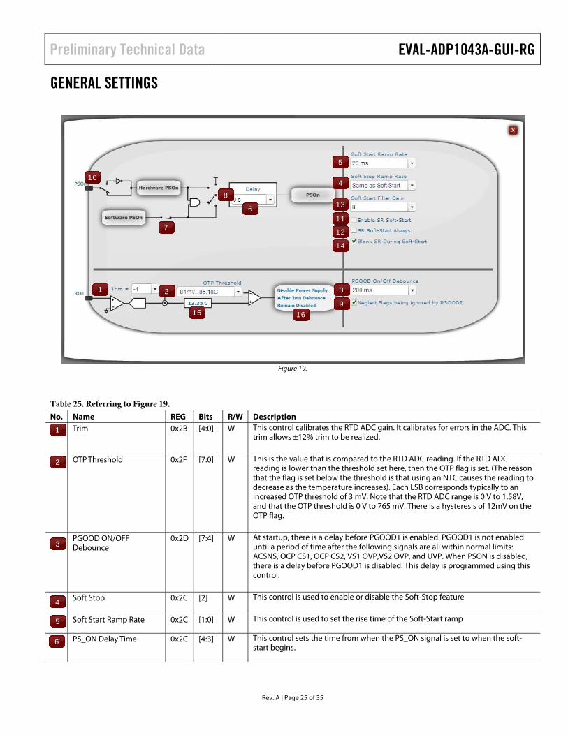
Table 25. Referring to Figure 19. No. Name REG Bits R/W Description Trim 0x2B [4:0] W This control calibrates the RTD ADC gain. It calibrates for errors in the ADC. This
trim allows ±12% trim to be realized.
OTP Threshold 0x2F [7:0] W This is the value that is compared to the RTD ADC reading. If the RTD ADCreading is lower than the threshold set here, then the OTP flag is set. (The reason that the flag is set below the threshold is that using an NTC causes the reading to decrease as the temperature increases). Each LSB corresponds typically to an increased OTP threshold of 3 mV. Note that the RTD ADC range is 0 V to 1.58V, and that the OTP threshold is 0 V to 765 mV. There is a hysteresis of 12mV on the OTP flag.
PGOOD ON/OFF Debounce
0x2D [7:4] W At startup, there is a delay before PGOOD1 is enabled. PGOOD1 is not enableduntil a period of time after the following signals are all within normal limits: ACSNS, OCP CS1, OCP CS2, VS1 OVP,VS2 OVP, and UVP. When PSON is disabled, there is a delay before PGOOD1 is disabled. This delay is programmed using this control.
Soft Stop 0x2C [2] W This control is used to enable or disable the Soft-Stop feature
Soft Start Ramp Rate 0x2C [1:0] W This control is used to set the rise time of the Soft-Start ramp
PS_ON Delay Time 0x2C [4:3] W This control sets the time from when the PS_ON signal is set to when the soft-start begins.
1 2 3
4
5
6
7
8
9
10
11
12
13
14
15
1
2
3
4
5
6
16

EVAL-ADP1043A-GUI-RG Preliminary Technical Data
Rev. A | Page 26 of 35
Table 26. Referring to Figure 19. No. Name REG Bits R/W Description PS ON 0x2C [5] W This control turns ON or OFF the PSON control signal when Software PSON is
selected.
PSON Type 0x2C [7:6] W This control selects between the different Software and Hardware PSON options.
Neglect Flags being ignored by PGOOD2
0x2D [3] W 0 = Any flag can set the PGOOD2 pin1 = Any flag that is not Ignored can set the PGood2 pin.
PSON Polarity 0x2D [0] W This control sets the polarity of the PSON input pin: If Inverted then low = on
Enable SR Soft-Start 0x54 [0] W Setting this means that the SR signals will have a soft-start function
SR Soft-Start Always 0x54 [1] W Checked = SR signals will soft-start every time they are enabled. Unchecked = SR Signals will soft-start only the first time that they are enabled.
Soft-Start Filter Setting 0x5F [1:0] W This control determines the bandwidth of the low pass digital filter that is used during soft-start
Blank SR During Soft Start
0x0F [7] W Setting this checkbox means that SR is ignored until the end of the soft-start ramp time.
Temperature 0x1A [15:4] R This value displays the temperature in degrees Celsius, which is converted from the voltage measured at the RTD pin.
OTP Action
0x0B [5:4] W This control sets the action that the ADP1043A needs to take once the flag is set.
Timing [7] W This control sets a debounce between the flag being set and the action that the ADP1043A needs to take.
Resolve Issue [6] W This control selects whether to re-enable ADP1043A or remain disabled after the flag is set.
7
8
9
10
11
12
13
15
14
16

Preliminary Technical Data EVAL-ADP1043A-GUI-RG
Rev. A | Page 27 of 35
FLAG SETTINGS
Figure 20.
Table 27. Referring to Figure 20. No. Name REG Bits R/W Description CS1 Fast OCP
Action 0x08
[5:4] W This control sets the action that the ADP1043A performs once this flag is set.
Timing 0x08 0x27
[7] [7:6]
W This sets the debounce between the flag being set and the action.
Resolve Issue [6] W This sets whether to re-enable or remain disabled after the flag is set.
CS1 Accurate OCP Action
0x08 [1:0] W This control sets the action that the ADP1043A needs to take once the flag is set.
Timing 0x08 0x0E
[3] [4:2]
W This control sets a debounce between the flag being set and the action that the ADP1043A needs to take.
Resolve Issue [2] W This control selects whether to re-enable ADP1043A or remain disabled after the flag is set.
CS2 Accurate OCP Action
0x09 [5:4] W This control sets the action that the ADP1043A needs to take once the flag is set.
Timing 0x09 0x0E
[7] [4:2]
W This control sets a debounce between the flag being set and the action that the ADP1043A needs to take.
Resolve Issue [6] W This control selects whether to re-enable ADP1043A or remain disabled after the flag is set.
1
2
3
4
5
6
7
8
9
10
11
12
13
14
15
1
3
16
2

EVAL-ADP1043A-GUI-RG Preliminary Technical Data
Rev. A | Page 28 of 35
Table 28. Referring to Figure 20. No. Name REG Bits R/W Description Line impedance
Action 0x0C [1:0] W This control sets the action that the ADP1043A needs to take once the flag is set.
Timing [3] W This control sets a debounce between the flag being set and the action that the ADP1043A needs to take.
Resolve Issue [2] W This control selects whether to re-enable ADP1043A or remain disabled after the flag is set.
UVP Action
0x0B [1:0] W This control sets the action that the ADP1043A needs to take once the flag is set.
Timing [3] W This control sets a debounce between the flag being set and the action that the ADP1043A needs to take.
Resolve Issue [2] W This control selects whether to re-enable ADP1043A or remain disabled after the flag is set.
Reverse Voltage (Accurate OrFET Threshold) Action
0x0C [5:4] W This control sets the action that the ADP1043A needs to take once the flag is set.
Timing [7] W This control sets a debounce between the flag being set and the action that the ADP1043A needs to take.
Resolve Issue [6] W This control selects whether to re-enable ADP1043A or remain disabled after the flag is set.
Load OVP (VS2 or VS3) Action
0x09 [1:0] W This control sets the action that the ADP1043A needs to take once the flag is set.
Timing [3] W This control sets a debounce between the flag being set and the action that the ADP1043A needs to take.
Resolve Issue [2] W This control selects whether to re-enable ADP1043A or remain disabled after the flag is set.
Local OVP (VS1) Action
0x0A [5:4] W This control sets the action that the ADP1043A needs to take once the flag is set.
Timing [7] W This control sets a debounce between the flag being set and the action that the ADP1043A needs to take.
Resolve Issue [6] W This control selects whether to re-enable ADP1043A or remain disabled after the flag is set.
OTP Action
0x0B [5:4] W This control sets the action that the ADP1043A needs to take once the flag is set.
Timing [7] W This control sets a debounce between the flag being set and the action that the ADP1043A needs to take.
Resolve Issue [6] W This control selects whether to re-enable ADP1043A or remain disabled after the flag is set.
4
5
6
7
8
9

Preliminary Technical Data EVAL-ADP1043A-GUI-RG
Rev. A | Page 29 of 35
Table 29. Referring to Figure 20. No. Name REG Bits R/W Description Share Bus
Action 0x0D [5:4] W This control sets the action that the ADP1043A needs to take once the flag is set.
Timing [7] W This control sets a debounce between the flag being set and the action that the ADP1043A needs to take.
Resolve Issue [6] W This control selects whether to re-enable ADP1043A or remain disabled after the flag is set.
External Flag Input (FLAGIN) Action
0x0A [1:0] W This control sets the action that the ADP1043A needs to take once the flag is set.
Timing [3] W This control sets a debounce between the flag being set and the action that the ADP1043A needs to take.
Resolve Issue [2] W This control selects whether to re-enable ADP1043A or remain disabled after the flag is set.
ACSNS Action
0x0D [1:0] W This control sets the action that the ADP1043A needs to take once the flag is set.
Timing [3] W This control sets a debounce between the flag being set and the action that the ADP1043A needs to take.
Resolve Issue [2] W This control selects whether to re-enable ADP1043A or remain disabled after the flag is set.
Power Supply Re-Enable Time
0x0E [1:0] W This control sets the Power Supply re-enable time
VDD / VCORE OV 0x0E [7] W Setting this bit means that the VDD OV and VCORE OV Flags will be ignored
Timing [5] W This control sets a debounce between the flag being set and the action that the ADP1043A needs to take.
Resolve Issue [6] W Setting this bit to 1 means that if the part shuts down, it will download EEPROM contents again before restarting. Setting this bit to 0 means that the part shuts down. It does not download EEPROM.
Blank Flag During Soft Start
0x0F [6:0] W Setting this checkbox means that corresponding flag is ignored until the end of the soft-start ramp time.
Flag Shutdown 0x34 [7] W This bit is only valid when the OUTAUX is used for regulation. Checked: When any flag decides to shutdown the power supply, OUTAUX PWM is immediately shutdown, and all other PWM’s are shutdown at the end of the switching cycle. Un-Checked: When any flag decides to shutdown the power supply, OUTAUX PWM is immediately shutdown, and all other PWM’s are also immediately shutdown.
10
14
13
16
15
11
12

EVAL-ADP1043A-GUI-RG Preliminary Technical Data
Rev. A | Page 30 of 35
MONITOR
Figure 21.
Table 30. Referring to Figure 21. No. Name REG Bits R/W Description I/P Voltage This indicator displays the input voltage calculated by the GUI using the duty
cycle, VS3 and the N1:N2 values
I/P Current 0x13 [15:4] R This value displays the current measured on the primary side. The CS1 ADC gives a value corresponding to the voltage on the CS1 pin, using the Rcs1 resistance value, the software calculates the current at that pin and then scales it using the N1:N2current transformer ratio
O/P Voltage 0x17 [15:4] R This value displays the voltage measured at the VS3 pin and scaled using the R1 and R2 values entered by the user.
O/P Current 0x18 [15:4] R This value displays the output current. The CS2 ADC gives a value corresponding to the voltage drop across the CS2 pins, using the Rsense resistance value, the software calculates the output current and is scaled using the CS2 Nominal Voltage Setting
VS1 0x15 [15:4] R This value displays the voltage measured at the VS1 pin and scaled using the R1 and R2 values entered by the user.
VS2 0x16 [15:4] R This value displays the voltage measured at the VS2 pin and scaled using the R1 and R2 values entered by the user.
SR OFF 0x00 [3] R Red = Sync rects are disabled. This flag is enabled when any of these threecases is true: • SR1 and SR2 are disabled by the user. • The load current has fallen below the threshold in Register 0x3C. • A flag that was configured to disable the sync rects has been set.
1
2
3
4
5 6
7
8
9
1
2
1
5
4
6
7
3

Preliminary Technical Data EVAL-ADP1043A-GUI-RG
Rev. A | Page 31 of 35
Table 31. Referring to Figure 21. No. Name REG Bits R/W Description OrFET 0x00 [6] R Red = OrFET control signal at the GATE pin (Pin 16) is off.
ADP1043A Monitor
Blocks The grey block represents ADP1043A and the blue blocks represent the various
monitor blocks of the ADP1043A. These blue blocks can be clicked to open the corresponding window for monitor
8
9

EVAL-ADP1043A-GUI-RG Preliminary Technical Data
Rev. A | Page 32 of 35
FLAGS AND POWER MONITORING
Figure 22.
Table 32. Referring to Figure 22. No. Name REG Bits R/W Description Power Supply 0x00 [7] R Red = Power supply is off. All PWM outputs are disabled. This bit stays
high until a PS ON is performed.
OrFET 0x00 [6] R Red = OrFET control signal at the GATE pin (Pin 16) is off.
PGOOD1 Fault 0x00 [5] R Red = Power-good 1 fault. At least one of the following is out of range:ACSNS, OCP CS1, OCP CS2, VS1 OVP, VS2 OVP, or UVP.
PGOOD2 Fault 0x00 [4] R Red = Power-good 2 fault. Any of these flag has been set: PowerSupply, OrFET, Fast OCP CS1, OCP CS1, OCP CS2, Voltage Continuity, UVP, Accurate OrFET Disable, VDDUV, VCORE OV, VDD OV, Load OVP, Local OVP, OTP, CRC Fault, EEPROM Unlocked
SR OFF 0x00 [3] R Red = Sync rects are disabled. This flag is enabled when any of these threecases is true: • SR1 and SR2 are disabled by the user. • The load current has fallen below the threshold in Register 0x3C. • A flag that was configured to disable the sync rects has been set.
Fast OCP (CS1) 0x00 [2] R Red = Fast OCP current is above its Over Current Protection limit. This is a1.2V threshold on the CS1 pin. Fast OCP is a comparator
OCP CS1 0x00 [1] R Red = CS1 current is above its Accurate Over Current Protection limit
OCP CS2 0x00 [0] R Red = CS2 current is above its Accurate Over Current Protection limit
1
1
2 3 4
5 6 7 8 9 10 11 12 13 14 15
16
17
18
19

Preliminary Technical Data EVAL-ADP1043A-GUI-RG
Rev. A | Page 33 of 35
Table 33. Referring to Figure 22. No. Name REG Bits R/W Description Voltage Continuity 0x01 [7] R Red = Voltage differential between VS1, VS2, VS3 pins is outside
limits. Either (VS1 − VS2) > 100 mV or (VS2 − VS3) > 100 mV.
UVP 0x01 [6] R Red = VS1 is below its undervoltage limit.
Accurate OrFET Disable 0x01 [5] R Red = Reverse voltage across CS2 pins is above limit. This is theAccurate OrFET Reverse Voltage.
VDD UV 0x01 [4] R Red = VDD is below limit.
VCORE OV 0x01 [3] R Red = 2.5 V VCORE is above limit.
VDD OV 0x01 [2] R Red = VDD is above limit. The I2C interface stays functional, but aPS_ON toggle is required to restart the power supply.
Load OVP 0x01 [1] R Red = VS2 or VS3 is above its overvoltage limit.
Local OVP 0x01 [0] R Red = VS1 is above its overvoltage limit.
OTP 0x02 [7] R Red = Temperature is above OTP limit.
Reserved 0x02 [6] R Reserved
Share Bus 0x02 [5] R Red = Current share is outside regulation limit.
Constant Current 0x02 [4] R Red = Power supply is operating in constant current mode.
Reserved 0x02 [3] R Reserved.
Line Impedance 0x02 [2] R Red = Line impedance between VS2 and VS3 is above limit.
Soft-Start Filter 0x02 [1] R Red = The Soft-Start Filter is in use
External Flag 0x02 [0] R Red = The external flag pin (FLAGIN) is set.
Reserved 0x03 [7] R Reserved.
Modulation 0x03 [6] R Red = Modulation is at either minimum or maximum limit.
Address 0x03 [5] R Red = The ADDRESS resistor is not correct.
Light Load Mode 0x03 [4] R Red = The system is in Light Load mode.
Reserved 0x03 [3] R Reserved.
ACSNS 0x03 [2] R Red = The ac sense timing or amplitude is not correct. The AC Sensecomparator has not tripped for one switching cycle.
CRC Fault 0x03 [1] R Red = The EEPROM contents downloaded are incorrect
EEPROM Unlocked 0x03 [0] R Red = The EEPROM is unlocked.
2
3
4

EVAL-ADP1043A-GUI-RG Preliminary Technical Data
Rev. A | Page 34 of 35
Table 34. Referring to Figure 22. No. Name REG Bits R/W Description I/P Voltage This indicator displays the input voltage calculated by the GUI using the duty
cycle, VS3 and the N1:N2 values
I/P Current 0x13 [15:4] R This value displays the current measured on the primary side. The CS1 ADC gives a value corresponding to the voltage on the CS1 pin, using the Rcs1 resistance value, the software calculates the current at that pin and then scales it using the N1:N2current transformer ratio
I/P Power This indicator displays the input power which is calculated using I/P Voltage and I/P Current
O/P Voltage 0x17 [15:4] R This value displays the voltage measured at the VS3 pin and scaled using the R1 and R2 values entered by the user.
O/P Current 0x18 [15:4] R This value displays the output current. The CS2 ADC gives a value corresponding to the voltage drop across the CS2 pins, using the Rsense resistance value, the software calculates the output current and is scaled using the CS2 Nominal Voltage Setting
O/P Power This indicator displays the input power which is calculated using O/P Voltage and O/P Current
VS1 0x15 [15:4] R This value displays the voltage measured at the VS1 pin and scaled using the R1 and R2 values entered by the user.
VS2 0x16 [15:4] R This value displays the voltage measured at the VS2 pin and scaled using the R1 and R2 values entered by the user.
Temperature 0x1A [15:4] R This value displays the temperature in degrees Celsius, which is converted from the voltage measured at the RTD pin.
Share Bus 0x1D [7:0] R This indicator displays share bus voltage information. If the power supply is themaster, this register will output zero.
Modulation Value 0x1E [7:0] R This indicator displays the amount of modulation from 0% to 100% that is being placed on the modulating edges.
Slave / Master 0x1D [7:0] R This indicator displays if the ADP1043A is in the Master Mode or Slave Mode.
Grey Lines These grey lines represent the various threshold levels for the indicator it is on.
Get First Flag 0x10 [3:0] R This button gets the flag that was set first. Restarting the power supply resets this value. Pressing this button also resets the value.
1st 0x10 [3:0] R This indicator represents the first flag that was set.
5
6
8
7 1
2
2
10
9
12
13
14
16
15
11
17
18
19

Preliminary Technical Data EVAL-ADP1043A-GUI-RG
Rev. A | Page 35 of 35
©2007 Analog Devices, Inc. All rights reserved. Trademarks and registered trademarks are the property of their respective owners. D00000-0-1/07(A)